US20080050911A1 - Microfeature workpieces having conductive interconnect structures formed by chemically reactive processes, and associated systems and methods - Google Patents
Microfeature workpieces having conductive interconnect structures formed by chemically reactive processes, and associated systems and methodsDownload PDFInfo
- Publication number
- US20080050911A1 US20080050911A1US11/511,690US51169006AUS2008050911A1US 20080050911 A1US20080050911 A1US 20080050911A1US 51169006 AUS51169006 AUS 51169006AUS 2008050911 A1US2008050911 A1US 2008050911A1
- Authority
- US
- United States
- Prior art keywords
- lining
- conductive
- copper
- microfeature workpiece
- reacting
- Prior art date
- Legal status (The legal status is an assumption and is not a legal conclusion. Google has not performed a legal analysis and makes no representation as to the accuracy of the status listed.)
- Granted
Links
Images


Classifications
- H—ELECTRICITY
- H01—ELECTRIC ELEMENTS
- H01L—SEMICONDUCTOR DEVICES NOT COVERED BY CLASS H10
- H01L21/00—Processes or apparatus adapted for the manufacture or treatment of semiconductor or solid state devices or of parts thereof
- H01L21/70—Manufacture or treatment of devices consisting of a plurality of solid state components formed in or on a common substrate or of parts thereof; Manufacture of integrated circuit devices or of parts thereof
- H01L21/71—Manufacture of specific parts of devices defined in group H01L21/70
- H01L21/768—Applying interconnections to be used for carrying current between separate components within a device comprising conductors and dielectrics
- H01L21/76898—Applying interconnections to be used for carrying current between separate components within a device comprising conductors and dielectrics formed through a semiconductor substrate
- H—ELECTRICITY
- H01—ELECTRIC ELEMENTS
- H01L—SEMICONDUCTOR DEVICES NOT COVERED BY CLASS H10
- H01L21/00—Processes or apparatus adapted for the manufacture or treatment of semiconductor or solid state devices or of parts thereof
- H01L21/70—Manufacture or treatment of devices consisting of a plurality of solid state components formed in or on a common substrate or of parts thereof; Manufacture of integrated circuit devices or of parts thereof
- H01L21/71—Manufacture of specific parts of devices defined in group H01L21/70
- H01L21/768—Applying interconnections to be used for carrying current between separate components within a device comprising conductors and dielectrics
- H01L21/76838—Applying interconnections to be used for carrying current between separate components within a device comprising conductors and dielectrics characterised by the formation and the after-treatment of the conductors
- H01L21/76841—Barrier, adhesion or liner layers
- H01L21/76843—Barrier, adhesion or liner layers formed in openings in a dielectric
- H01L21/76846—Layer combinations
- H—ELECTRICITY
- H01—ELECTRIC ELEMENTS
- H01L—SEMICONDUCTOR DEVICES NOT COVERED BY CLASS H10
- H01L21/00—Processes or apparatus adapted for the manufacture or treatment of semiconductor or solid state devices or of parts thereof
- H01L21/70—Manufacture or treatment of devices consisting of a plurality of solid state components formed in or on a common substrate or of parts thereof; Manufacture of integrated circuit devices or of parts thereof
- H01L21/71—Manufacture of specific parts of devices defined in group H01L21/70
- H01L21/768—Applying interconnections to be used for carrying current between separate components within a device comprising conductors and dielectrics
- H01L21/76838—Applying interconnections to be used for carrying current between separate components within a device comprising conductors and dielectrics characterised by the formation and the after-treatment of the conductors
- H01L21/76841—Barrier, adhesion or liner layers
- H01L21/76853—Barrier, adhesion or liner layers characterized by particular after-treatment steps
- H01L21/76855—After-treatment introducing at least one additional element into the layer
- H01L21/76856—After-treatment introducing at least one additional element into the layer by treatment in plasmas or gaseous environments, e.g. nitriding a refractory metal liner
- H—ELECTRICITY
- H01—ELECTRIC ELEMENTS
- H01L—SEMICONDUCTOR DEVICES NOT COVERED BY CLASS H10
- H01L21/00—Processes or apparatus adapted for the manufacture or treatment of semiconductor or solid state devices or of parts thereof
- H01L21/70—Manufacture or treatment of devices consisting of a plurality of solid state components formed in or on a common substrate or of parts thereof; Manufacture of integrated circuit devices or of parts thereof
- H01L21/71—Manufacture of specific parts of devices defined in group H01L21/70
- H01L21/768—Applying interconnections to be used for carrying current between separate components within a device comprising conductors and dielectrics
- H01L21/76838—Applying interconnections to be used for carrying current between separate components within a device comprising conductors and dielectrics characterised by the formation and the after-treatment of the conductors
- H01L21/76841—Barrier, adhesion or liner layers
- H01L21/76868—Forming or treating discontinuous thin films, e.g. repair, enhancement or reinforcement of discontinuous thin films
- H—ELECTRICITY
- H01—ELECTRIC ELEMENTS
- H01L—SEMICONDUCTOR DEVICES NOT COVERED BY CLASS H10
- H01L24/00—Arrangements for connecting or disconnecting semiconductor or solid-state bodies; Methods or apparatus related thereto
- H01L24/01—Means for bonding being attached to, or being formed on, the surface to be connected, e.g. chip-to-package, die-attach, "first-level" interconnects; Manufacturing methods related thereto
- H01L24/02—Bonding areas ; Manufacturing methods related thereto
- H01L24/03—Manufacturing methods
- H—ELECTRICITY
- H01—ELECTRIC ELEMENTS
- H01L—SEMICONDUCTOR DEVICES NOT COVERED BY CLASS H10
- H01L24/00—Arrangements for connecting or disconnecting semiconductor or solid-state bodies; Methods or apparatus related thereto
- H01L24/01—Means for bonding being attached to, or being formed on, the surface to be connected, e.g. chip-to-package, die-attach, "first-level" interconnects; Manufacturing methods related thereto
- H01L24/02—Bonding areas ; Manufacturing methods related thereto
- H01L24/04—Structure, shape, material or disposition of the bonding areas prior to the connecting process
- H01L24/05—Structure, shape, material or disposition of the bonding areas prior to the connecting process of an individual bonding area
- H—ELECTRICITY
- H01—ELECTRIC ELEMENTS
- H01L—SEMICONDUCTOR DEVICES NOT COVERED BY CLASS H10
- H01L2224/00—Indexing scheme for arrangements for connecting or disconnecting semiconductor or solid-state bodies and methods related thereto as covered by H01L24/00
- H01L2224/01—Means for bonding being attached to, or being formed on, the surface to be connected, e.g. chip-to-package, die-attach, "first-level" interconnects; Manufacturing methods related thereto
- H01L2224/02—Bonding areas; Manufacturing methods related thereto
- H01L2224/0212—Auxiliary members for bonding areas, e.g. spacers
- H01L2224/02122—Auxiliary members for bonding areas, e.g. spacers being formed on the semiconductor or solid-state body
- H01L2224/02123—Auxiliary members for bonding areas, e.g. spacers being formed on the semiconductor or solid-state body inside the bonding area
- H01L2224/02125—Reinforcing structures
- H01L2224/02126—Collar structures
- H—ELECTRICITY
- H01—ELECTRIC ELEMENTS
- H01L—SEMICONDUCTOR DEVICES NOT COVERED BY CLASS H10
- H01L2224/00—Indexing scheme for arrangements for connecting or disconnecting semiconductor or solid-state bodies and methods related thereto as covered by H01L24/00
- H01L2224/01—Means for bonding being attached to, or being formed on, the surface to be connected, e.g. chip-to-package, die-attach, "first-level" interconnects; Manufacturing methods related thereto
- H01L2224/02—Bonding areas; Manufacturing methods related thereto
- H01L2224/04—Structure, shape, material or disposition of the bonding areas prior to the connecting process
- H01L2224/05—Structure, shape, material or disposition of the bonding areas prior to the connecting process of an individual bonding area
- H01L2224/05001—Internal layers
- H01L2224/05005—Structure
- H01L2224/05009—Bonding area integrally formed with a via connection of the semiconductor or solid-state body
- H—ELECTRICITY
- H01—ELECTRIC ELEMENTS
- H01L—SEMICONDUCTOR DEVICES NOT COVERED BY CLASS H10
- H01L2224/00—Indexing scheme for arrangements for connecting or disconnecting semiconductor or solid-state bodies and methods related thereto as covered by H01L24/00
- H01L2224/01—Means for bonding being attached to, or being formed on, the surface to be connected, e.g. chip-to-package, die-attach, "first-level" interconnects; Manufacturing methods related thereto
- H01L2224/02—Bonding areas; Manufacturing methods related thereto
- H01L2224/04—Structure, shape, material or disposition of the bonding areas prior to the connecting process
- H01L2224/05—Structure, shape, material or disposition of the bonding areas prior to the connecting process of an individual bonding area
- H01L2224/05001—Internal layers
- H01L2224/0502—Disposition
- H01L2224/05025—Disposition the internal layer being disposed on a via connection of the semiconductor or solid-state body
- H—ELECTRICITY
- H01—ELECTRIC ELEMENTS
- H01L—SEMICONDUCTOR DEVICES NOT COVERED BY CLASS H10
- H01L2224/00—Indexing scheme for arrangements for connecting or disconnecting semiconductor or solid-state bodies and methods related thereto as covered by H01L24/00
- H01L2224/01—Means for bonding being attached to, or being formed on, the surface to be connected, e.g. chip-to-package, die-attach, "first-level" interconnects; Manufacturing methods related thereto
- H01L2224/02—Bonding areas; Manufacturing methods related thereto
- H01L2224/04—Structure, shape, material or disposition of the bonding areas prior to the connecting process
- H01L2224/05—Structure, shape, material or disposition of the bonding areas prior to the connecting process of an individual bonding area
- H01L2224/05001—Internal layers
- H01L2224/05099—Material
- H01L2224/051—Material with a principal constituent of the material being a metal or a metalloid, e.g. boron [B], silicon [Si], germanium [Ge], arsenic [As], antimony [Sb], tellurium [Te] and polonium [Po], and alloys thereof
- H01L2224/05138—Material with a principal constituent of the material being a metal or a metalloid, e.g. boron [B], silicon [Si], germanium [Ge], arsenic [As], antimony [Sb], tellurium [Te] and polonium [Po], and alloys thereof the principal constituent melting at a temperature of greater than or equal to 950°C and less than 1550°C
- H01L2224/05147—Copper [Cu] as principal constituent
- H—ELECTRICITY
- H01—ELECTRIC ELEMENTS
- H01L—SEMICONDUCTOR DEVICES NOT COVERED BY CLASS H10
- H01L2224/00—Indexing scheme for arrangements for connecting or disconnecting semiconductor or solid-state bodies and methods related thereto as covered by H01L24/00
- H01L2224/01—Means for bonding being attached to, or being formed on, the surface to be connected, e.g. chip-to-package, die-attach, "first-level" interconnects; Manufacturing methods related thereto
- H01L2224/02—Bonding areas; Manufacturing methods related thereto
- H01L2224/04—Structure, shape, material or disposition of the bonding areas prior to the connecting process
- H01L2224/05—Structure, shape, material or disposition of the bonding areas prior to the connecting process of an individual bonding area
- H01L2224/05001—Internal layers
- H01L2224/05099—Material
- H01L2224/051—Material with a principal constituent of the material being a metal or a metalloid, e.g. boron [B], silicon [Si], germanium [Ge], arsenic [As], antimony [Sb], tellurium [Te] and polonium [Po], and alloys thereof
- H01L2224/05138—Material with a principal constituent of the material being a metal or a metalloid, e.g. boron [B], silicon [Si], germanium [Ge], arsenic [As], antimony [Sb], tellurium [Te] and polonium [Po], and alloys thereof the principal constituent melting at a temperature of greater than or equal to 950°C and less than 1550°C
- H01L2224/05155—Nickel [Ni] as principal constituent
- H—ELECTRICITY
- H01—ELECTRIC ELEMENTS
- H01L—SEMICONDUCTOR DEVICES NOT COVERED BY CLASS H10
- H01L2224/00—Indexing scheme for arrangements for connecting or disconnecting semiconductor or solid-state bodies and methods related thereto as covered by H01L24/00
- H01L2224/01—Means for bonding being attached to, or being formed on, the surface to be connected, e.g. chip-to-package, die-attach, "first-level" interconnects; Manufacturing methods related thereto
- H01L2224/02—Bonding areas; Manufacturing methods related thereto
- H01L2224/04—Structure, shape, material or disposition of the bonding areas prior to the connecting process
- H01L2224/05—Structure, shape, material or disposition of the bonding areas prior to the connecting process of an individual bonding area
- H01L2224/05001—Internal layers
- H01L2224/05099—Material
- H01L2224/051—Material with a principal constituent of the material being a metal or a metalloid, e.g. boron [B], silicon [Si], germanium [Ge], arsenic [As], antimony [Sb], tellurium [Te] and polonium [Po], and alloys thereof
- H01L2224/05163—Material with a principal constituent of the material being a metal or a metalloid, e.g. boron [B], silicon [Si], germanium [Ge], arsenic [As], antimony [Sb], tellurium [Te] and polonium [Po], and alloys thereof the principal constituent melting at a temperature of greater than 1550°C
- H01L2224/05181—Tantalum [Ta] as principal constituent
- H—ELECTRICITY
- H01—ELECTRIC ELEMENTS
- H01L—SEMICONDUCTOR DEVICES NOT COVERED BY CLASS H10
- H01L2224/00—Indexing scheme for arrangements for connecting or disconnecting semiconductor or solid-state bodies and methods related thereto as covered by H01L24/00
- H01L2224/01—Means for bonding being attached to, or being formed on, the surface to be connected, e.g. chip-to-package, die-attach, "first-level" interconnects; Manufacturing methods related thereto
- H01L2224/02—Bonding areas; Manufacturing methods related thereto
- H01L2224/04—Structure, shape, material or disposition of the bonding areas prior to the connecting process
- H01L2224/05—Structure, shape, material or disposition of the bonding areas prior to the connecting process of an individual bonding area
- H01L2224/05001—Internal layers
- H01L2224/05099—Material
- H01L2224/051—Material with a principal constituent of the material being a metal or a metalloid, e.g. boron [B], silicon [Si], germanium [Ge], arsenic [As], antimony [Sb], tellurium [Te] and polonium [Po], and alloys thereof
- H01L2224/05163—Material with a principal constituent of the material being a metal or a metalloid, e.g. boron [B], silicon [Si], germanium [Ge], arsenic [As], antimony [Sb], tellurium [Te] and polonium [Po], and alloys thereof the principal constituent melting at a temperature of greater than 1550°C
- H01L2224/05184—Tungsten [W] as principal constituent
- H—ELECTRICITY
- H01—ELECTRIC ELEMENTS
- H01L—SEMICONDUCTOR DEVICES NOT COVERED BY CLASS H10
- H01L2224/00—Indexing scheme for arrangements for connecting or disconnecting semiconductor or solid-state bodies and methods related thereto as covered by H01L24/00
- H01L2224/01—Means for bonding being attached to, or being formed on, the surface to be connected, e.g. chip-to-package, die-attach, "first-level" interconnects; Manufacturing methods related thereto
- H01L2224/02—Bonding areas; Manufacturing methods related thereto
- H01L2224/04—Structure, shape, material or disposition of the bonding areas prior to the connecting process
- H01L2224/05—Structure, shape, material or disposition of the bonding areas prior to the connecting process of an individual bonding area
- H01L2224/0554—External layer
- H01L2224/0556—Disposition
- H01L2224/0557—Disposition the external layer being disposed on a via connection of the semiconductor or solid-state body
- H—ELECTRICITY
- H01—ELECTRIC ELEMENTS
- H01L—SEMICONDUCTOR DEVICES NOT COVERED BY CLASS H10
- H01L2224/00—Indexing scheme for arrangements for connecting or disconnecting semiconductor or solid-state bodies and methods related thereto as covered by H01L24/00
- H01L2224/01—Means for bonding being attached to, or being formed on, the surface to be connected, e.g. chip-to-package, die-attach, "first-level" interconnects; Manufacturing methods related thereto
- H01L2224/02—Bonding areas; Manufacturing methods related thereto
- H01L2224/04—Structure, shape, material or disposition of the bonding areas prior to the connecting process
- H01L2224/05—Structure, shape, material or disposition of the bonding areas prior to the connecting process of an individual bonding area
- H01L2224/0554—External layer
- H01L2224/05599—Material
- H01L2224/056—Material with a principal constituent of the material being a metal or a metalloid, e.g. boron [B], silicon [Si], germanium [Ge], arsenic [As], antimony [Sb], tellurium [Te] and polonium [Po], and alloys thereof
- H01L2224/05638—Material with a principal constituent of the material being a metal or a metalloid, e.g. boron [B], silicon [Si], germanium [Ge], arsenic [As], antimony [Sb], tellurium [Te] and polonium [Po], and alloys thereof the principal constituent melting at a temperature of greater than or equal to 950°C and less than 1550°C
- H01L2224/05647—Copper [Cu] as principal constituent
- H—ELECTRICITY
- H01—ELECTRIC ELEMENTS
- H01L—SEMICONDUCTOR DEVICES NOT COVERED BY CLASS H10
- H01L2224/00—Indexing scheme for arrangements for connecting or disconnecting semiconductor or solid-state bodies and methods related thereto as covered by H01L24/00
- H01L2224/01—Means for bonding being attached to, or being formed on, the surface to be connected, e.g. chip-to-package, die-attach, "first-level" interconnects; Manufacturing methods related thereto
- H01L2224/10—Bump connectors; Manufacturing methods related thereto
- H01L2224/12—Structure, shape, material or disposition of the bump connectors prior to the connecting process
- H01L2224/13—Structure, shape, material or disposition of the bump connectors prior to the connecting process of an individual bump connector
- H01L2224/13001—Core members of the bump connector
- H01L2224/1302—Disposition
- H01L2224/13025—Disposition the bump connector being disposed on a via connection of the semiconductor or solid-state body
- H—ELECTRICITY
- H01—ELECTRIC ELEMENTS
- H01L—SEMICONDUCTOR DEVICES NOT COVERED BY CLASS H10
- H01L2224/00—Indexing scheme for arrangements for connecting or disconnecting semiconductor or solid-state bodies and methods related thereto as covered by H01L24/00
- H01L2224/01—Means for bonding being attached to, or being formed on, the surface to be connected, e.g. chip-to-package, die-attach, "first-level" interconnects; Manufacturing methods related thereto
- H01L2224/10—Bump connectors; Manufacturing methods related thereto
- H01L2224/15—Structure, shape, material or disposition of the bump connectors after the connecting process
- H01L2224/16—Structure, shape, material or disposition of the bump connectors after the connecting process of an individual bump connector
- H—ELECTRICITY
- H01—ELECTRIC ELEMENTS
- H01L—SEMICONDUCTOR DEVICES NOT COVERED BY CLASS H10
- H01L2225/00—Details relating to assemblies covered by the group H01L25/00 but not provided for in its subgroups
- H01L2225/03—All the devices being of a type provided for in the same main group of the same subclass of class H10, e.g. assemblies of rectifier diodes
- H01L2225/04—All the devices being of a type provided for in the same main group of the same subclass of class H10, e.g. assemblies of rectifier diodes the devices not having separate containers
- H01L2225/065—All the devices being of a type provided for in the same main group of the same subclass of class H10
- H01L2225/06503—Stacked arrangements of devices
- H01L2225/06513—Bump or bump-like direct electrical connections between devices, e.g. flip-chip connection, solder bumps
- H—ELECTRICITY
- H01—ELECTRIC ELEMENTS
- H01L—SEMICONDUCTOR DEVICES NOT COVERED BY CLASS H10
- H01L2225/00—Details relating to assemblies covered by the group H01L25/00 but not provided for in its subgroups
- H01L2225/03—All the devices being of a type provided for in the same main group of the same subclass of class H10, e.g. assemblies of rectifier diodes
- H01L2225/04—All the devices being of a type provided for in the same main group of the same subclass of class H10, e.g. assemblies of rectifier diodes the devices not having separate containers
- H01L2225/065—All the devices being of a type provided for in the same main group of the same subclass of class H10
- H01L2225/06503—Stacked arrangements of devices
- H01L2225/06517—Bump or bump-like direct electrical connections from device to substrate
- H—ELECTRICITY
- H01—ELECTRIC ELEMENTS
- H01L—SEMICONDUCTOR DEVICES NOT COVERED BY CLASS H10
- H01L2225/00—Details relating to assemblies covered by the group H01L25/00 but not provided for in its subgroups
- H01L2225/03—All the devices being of a type provided for in the same main group of the same subclass of class H10, e.g. assemblies of rectifier diodes
- H01L2225/04—All the devices being of a type provided for in the same main group of the same subclass of class H10, e.g. assemblies of rectifier diodes the devices not having separate containers
- H01L2225/065—All the devices being of a type provided for in the same main group of the same subclass of class H10
- H01L2225/06503—Stacked arrangements of devices
- H01L2225/06541—Conductive via connections through the device, e.g. vertical interconnects, through silicon via [TSV]
- H—ELECTRICITY
- H01—ELECTRIC ELEMENTS
- H01L—SEMICONDUCTOR DEVICES NOT COVERED BY CLASS H10
- H01L24/00—Arrangements for connecting or disconnecting semiconductor or solid-state bodies; Methods or apparatus related thereto
- H01L24/01—Means for bonding being attached to, or being formed on, the surface to be connected, e.g. chip-to-package, die-attach, "first-level" interconnects; Manufacturing methods related thereto
- H01L24/10—Bump connectors ; Manufacturing methods related thereto
- H01L24/12—Structure, shape, material or disposition of the bump connectors prior to the connecting process
- H01L24/13—Structure, shape, material or disposition of the bump connectors prior to the connecting process of an individual bump connector
- H—ELECTRICITY
- H01—ELECTRIC ELEMENTS
- H01L—SEMICONDUCTOR DEVICES NOT COVERED BY CLASS H10
- H01L24/00—Arrangements for connecting or disconnecting semiconductor or solid-state bodies; Methods or apparatus related thereto
- H01L24/01—Means for bonding being attached to, or being formed on, the surface to be connected, e.g. chip-to-package, die-attach, "first-level" interconnects; Manufacturing methods related thereto
- H01L24/10—Bump connectors ; Manufacturing methods related thereto
- H01L24/12—Structure, shape, material or disposition of the bump connectors prior to the connecting process
- H01L24/14—Structure, shape, material or disposition of the bump connectors prior to the connecting process of a plurality of bump connectors
- H—ELECTRICITY
- H01—ELECTRIC ELEMENTS
- H01L—SEMICONDUCTOR DEVICES NOT COVERED BY CLASS H10
- H01L25/00—Assemblies consisting of a plurality of semiconductor or other solid state devices
- H01L25/03—Assemblies consisting of a plurality of semiconductor or other solid state devices all the devices being of a type provided for in a single subclass of subclasses H10B, H10D, H10F, H10H, H10K or H10N, e.g. assemblies of rectifier diodes
- H01L25/04—Assemblies consisting of a plurality of semiconductor or other solid state devices all the devices being of a type provided for in a single subclass of subclasses H10B, H10D, H10F, H10H, H10K or H10N, e.g. assemblies of rectifier diodes the devices not having separate containers
- H01L25/065—Assemblies consisting of a plurality of semiconductor or other solid state devices all the devices being of a type provided for in a single subclass of subclasses H10B, H10D, H10F, H10H, H10K or H10N, e.g. assemblies of rectifier diodes the devices not having separate containers the devices being of a type provided for in group H10D89/00
- H01L25/0657—Stacked arrangements of devices
- H—ELECTRICITY
- H01—ELECTRIC ELEMENTS
- H01L—SEMICONDUCTOR DEVICES NOT COVERED BY CLASS H10
- H01L2924/00—Indexing scheme for arrangements or methods for connecting or disconnecting semiconductor or solid-state bodies as covered by H01L24/00
- H01L2924/10—Details of semiconductor or other solid state devices to be connected
- H01L2924/11—Device type
- H01L2924/14—Integrated circuits
Definitions
- the present disclosureis directed generally toward microfeature workpieces having conductive interconnect structures formed by chemically reactive processes, and associated systems and methods, including microfeature workpieces having conductive interconnect vias at least partially filled with copper sulfide.
- Microelectronic imagersare used in digital cameras, wireless devices with picture capabilities, and many other applications. Many cell phones and Personal Digital Assistants (PDAs), for example, incorporate microelectronic imagers for capturing and sending pictures. The growth rate of microelectronic imagers has been steadily increasing as they become smaller and produce better images with higher pixel counts.
- Microelectronic imagersinclude image sensors that use Charged Coupled Device (CCD) systems, Complementary Metal-Oxide Semiconductor (CMOS) systems, or other solid-state systems.
- CCD image sensorshave been widely used in digital cameras and other applications.
- CMOS image sensorsare also quickly becoming very popular because they are expected to have low production costs, high yields, and small sizes.
- CMOS image sensorscan provide these advantages because they are manufactured using technology and equipment developed for fabricating semiconductor devices.
- CMOS image sensors, as well as CCD image sensorsare accordingly “packaged” to protect their delicate components and to provide external electrical contacts.
- imaging devicesinclude semiconductor dies having image sensors located on a front surface of the die to receive incoming radiation.
- the diesalso include bond pads for electrically coupling the sensors to other circuit elements.
- the bond padscan be positioned on the opposite side of the die from the sensors (e.g., on the back surface of the die).
- Through-wafer interconnectsTWIs are used to conduct electrical signals from the sensors and associated internal circuitry, through the die to the bond pads at the back surface.
- the TWIsare typically formed by making a blind via in the die, filling the via with solder, and then grinding the back surface of the die to expose the blind end of the via, which is used to form the bond pad. A solder ball can then be attached to the bond pad and can be reflowed to couple the die to external devices.
- solder within the viamay also tend to melt or at least soften.
- the solder within the viacan be pulled at least partially out of the via, or can otherwise undergo deformations and/or movement that can adversely affect the electrical continuity of the TWI.
- the electrical continuity of the TWImay be disrupted, causing the electrical connection between the image sensor and the external devices to fail.
- Another potential drawback associated with the foregoing approachis that the number of steps required to produce the TWI increases the cost of making the associated die.
- the use of solder in the blind viarequires forming a vent hole to allow gases within the via to escape as the solder enters. Even so, the solder may include voids, which can disrupt electrical continuity and in subsequent processes, expand and create electrical shorts.
- the processes required to dispose the solder in the viaare typically high-temperature processes, which can use up a significant portion of the thermal budget of the die. Accordingly, there is a need for an improved process for forming microfeature workpiece electrical connections, including connections between dies and external devices.
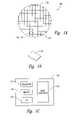
- FIG. 1Ais a partially schematic illustration of a representative microfeature workpiece carrying microfeature dies configured in accordance with embodiments of the invention.
- FIG. 1Bis a schematic illustration of a microfeature die singulated from the workpiece shown in FIG. 1A .
- FIG. 1Cis a schematic illustration of a system which can include one or more microfeature dies in accordance with embodiments of the invention.
- FIG. 1Dis a partially schematic, cross-sectional illustration of a portion of the workpiece prior to formation of a conductive structure in accordance with an embodiment of the invention.
- FIG. 1Eis an enlarged view of a portion of the workpiece shown in FIG. 1A .
- FIGS. 2A-2Killustrate a process for introducing conductive material in a via by using a chemical reaction in accordance with an embodiment of the invention.
- FIG. 3is an illustration of a substrate having features in accordance with another embodiment of the invention.
- microfeature workpieces having conductive vias formed by chemically reactive processesand associated systems and methods. Specific details of several embodiments of the invention are described below with reference to CMOS image sensors to provide a thorough understanding of these embodiments, but other embodiments can use CCD image sensors or other types of solid-state imaging devices. In still further embodiments, aspects of the invention can be practiced in connection with devices that do not include image sensors. Such devices include SRAM, DRAM, Flash, and other devices. In particular embodiments, the devices can be stacked on each other, and the vias can provide electrical communication among the stacked devices.
- microfeature workpieceand “workpiece” refer to substrates on and/in which microfeature electronic devices (including, but not limited to, image sensors) are integrally formed.
- a microfeature workpiececan include a wafer, and/or individual dies or combinations of dies that make up the wafer.
- Typical microfeature electronic devices of the workpieceinclude microfeature electronic circuits or components, thin-film recording heads, data storage elements, microfluidic devices and other products.
- Micromachines and micromechanical devicesare included within this definition because they are manufactured using much of the same technology that is used in the fabrication of integrated circuits.
- the substratescan be semi-conductive pieces (e.g., doped silicon wafers or gallium arsenide wafers), non-conductive pieces (e.g., various ceramic substrates), or conductive pieces.
- the workpiecesare generally round, and in other cases the workpieces can have other shapes, including rectilinear shapes.
- FIG. 1Ais a microfeature workpiece 100 in the form of a wafer 170 that includes multiple microfeature dies 120 . At least some of the processes described below may be conducted on the microfeature workpiece 100 at the wafer level, and other processes may be conducted on the individual microfeature dies 120 of the microfeature workpiece 100 after the dies 120 have been singulated from the larger wafer 170 . Accordingly, unless otherwise noted, structures and methods described below in the context of a “microfeature workpiece” can apply to the wafer 170 and/or the dies 120 that are formed from the wafer 170 .
- FIG. 1Bis a schematic illustration of an individual die 120 after it has been singulated from the wafer 170 shown in FIG. 1A .
- the die 120can include operable microelectronic structure, optionally encased within a protective encapsulant. Pins, bond pads, solder balls, and/other conductive structures provide electrical communication between structures within the die 120 and structures/devices located external to the die.
- the system 180can include a processor 181 , a memory 182 , input/output devices 183 , and/or other subsystems or components 184 .
- Microfeature workpiecese.g., in the form of microfeature dies and/or combinations of microfeature dies
- the resulting system 180can perform any of a wide variety of computing, processing, storage, sensor and/or other functions.
- representative systems 180include, without limitation, computers and/or other data processors, for example, desktop computers, laptop computers, Internet appliances, hand-held devices (e.g., palm-top computers, wearable computers, cellular or mobile phones, multi-processor systems, processor-based or programmable consumer electronics, network computers, mini computers).
- Other representative systems 180include cameras, light sensors, servers and associated server subsystems, display devices, and/or memory devices.
- Components of the system 180may be housed in a single unit or distributed over multiple, interconnected units, e.g., through a communications network.
- Componentscan accordingly include local and/or remote memory storage devices, and any of a wide variety of computer-readable media, including magnetic or optically readable or removable computer disks.
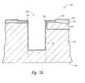
- FIG. 1Dis a side cross-sectional view of a portion of an imager workpiece 100 prior to the formation of conductive interconnect structures in accordance with an embodiment of the invention.
- the workpiece 100can include a substrate 101 with a plurality of dies 120 (e.g., imaging dies) formed in and/or on the substrate 101 .
- the substrate 101has a first side or surface 102 and a second side or surface 103 .
- the substrate 101can be a semiconductor wafer, with the dies 120 arranged in a die pattern on the wafer.
- Individual dies 120can include integrated circuitry 121 , a plurality of terminals or bond sites 122 (e.g., bond pads) electrically coupled to the integrated circuitry 121 with couplers 126 , and an image sensor 112 .
- the image sensors 112can be CMOS image sensors or CCD image sensors for capturing pictures or other images in the visible spectrum. In other embodiments, the image sensors 112 can detect radiation in other spectrums (e.g., IR or UV ranges).
- the bond sites 122 shown in FIG. 1Dare external features at the first side 102 of the substrate 101 . In other embodiments, however, the bond sites 122 can be internal features that are embedded at an intermediate depth within the substrate 101 .
- First and second dielectric layers 104 and 105can be located at the first side 102 to protect the underlying substrate 101 .
- FIG. 1Eis a side cross-sectional view of an area 1 E shown in FIG. 1D .
- This portion of the workpiece 100is representative of devices that include, but are not limited to, imager devices. Accordingly, the following discussion is also not limited to imager devices.
- the second dielectric layer 105has been patterned and etched to expose the bond site 122 .
- a mask 106is applied over the second dielectric layer 105 and patterned, as shown in FIG. 1E .
- the mask 106can be a layer of resist that is patterned according to the arrangement of bond sites 122 on the substrate 101 . Accordingly, the mask 106 can have an opening over each bond site 122 .
- a via 130has been formed in the workpiece 100 so as to extend into the substrate 101 through the bond site 122 and the first surface 102 .
- the via 130can be formed using any of a variety of techniques, including etching or laser drilling.
- the via 130can be a blind via, as shown in FIG. 2A , e.g., a via that does not extend entirely through the workpiece 100 and/or the substrate 101 .
- the via 130can extend entirely through the workpiece 100 and/or the substrate 101 , as indicated in dashed lines in FIG. 2A . Further details of representative methods for forming the via 130 are disclosed in pending U.S. patent application Ser. No. 11/169,546, filed Jun.
- a third dielectric layer 132is deposited onto the workpiece 100 to line the sidewalls 131 of the via 130 within the substrate 101 .
- the third dielectric layer 132electrically insulates components in the substrate 101 from an interconnect structure that is subsequently formed in the via 130 .
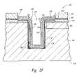
- a suitable etching processe.g., a spacer etch
- a spacer etchis used to remove portions of the third dielectric layer 132 that extend over the bond site 122 . Accordingly, at least part of the bond site 122 can be exposed for electrical coupling to conductive structures in the via 130 , as is described in greater detail below.
- a conductive barrier layer 133is then deposited onto the workpiece 100 over the third dielectric layer 132 so as to be in electrical contact with the bond site 122 .
- the barrier layer 133generally covers the second dielectric layer 105 and the bond site 122 in addition to the third dielectric layer 132 .
- the barrier layer 133is a layer of tantalum that is deposited onto the workpiece 100 using a physical vapor deposition (PVD) process.
- the thickness of the barrier layer 133is about 150 Angstroms.
- the barrier layer 133may be deposited onto the workpiece 100 using other vapor deposition processes, such as chemical vapor deposition (CVD), and/or may have a different thickness.
- the composition of the barrier layer 133is not limited to tantalum, but rather may be composed of tungsten or other suitable materials.
- a seed layer 134is deposited onto the barrier layer 133 .
- the seed layer 134can be deposited using vapor deposition techniques, such as PVD, CVD, atomic layer deposition, and/or plating.
- the seed layer 134can be composed of copper or other suitable materials.
- the thickness of the seed layer 134may be about 2000 Angstroms, but can be more or less depending upon the depth and aspect ratio of the via 130 .
- the seed layer 134may not uniformly cover the barrier layer 133 , such that the seed layer 134 has voids 135 within the via 130 . This can cause non-uniform electroplating in the via 130 and across the workpiece 100 .
- the seed layer 134When the seed layer 134 is deficient, it may be enhanced using a process that fills voids or noncontinuous regions of the seed layer 134 to form a more uniform seed layer. Referring to FIG. 2E , for example, voids 135 and/or noncontinuous regions of the seed layer 134 have been filled with additional material 136 , such as copper or another suitable material.
- additional material 136such as copper or another suitable material.
- a resist layer 107is deposited onto the seed layer 134 and is patterned to have an opening 108 over the bond site 122 and the via 130 .
- a first conductive lining or layer 137is then deposited onto the exposed portions of the seed layer 134 in the via 130 .
- the first conductive layer 137can include copper that is deposited onto the seed layer 134 in an electroless plating operation, or an electroplating operation, or by another suitable method. In the illustrated embodiment, the thickness of the first conductive layer 137 is about 1 micron. In other embodiments, the first conductive layer 137 may include other suitable materials and/or have a different thickness.
- a second conductive layer 147can then be deposited on the first conductive layer 137 .
- the second conductive layer 147can include nickel or another diffusion barrier that prevents or restricts migration of the material (e.g., copper) in the first conductive layer 137 .
- a third conductive layer 148can then be disposed on the second conductive layer 147 .
- the third conductive layer 148can also include copper.
- the combined thicknesses of the conductive layersis such that a space is located between opposing portions of the last-formed layer that face each other across the via 130 .
- the third conductive layer 148is deliberately configured so as to withstand a loss of material during the formation of a conductive chemical compound in the via 130 . Accordingly, the thickness of the third conductive layer 148 can be selected based on how much material from the third conductive layer 148 is expected to be used up in the formation of the compound.
- the second conductive layer 147can act as a barrier to limit the loss of material to material from the third conductive layer 148 , and prevent a loss of material from the first conductive layer 137 .
- the second conductive layer 147 and the third conductive layer 148can be eliminated, and the first conductive layer 137 alone can be made thick enough to withstand the loss of material during the reaction process.
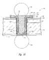
- the open space in the via 130is filled with solder (e.g., a mixture of tin, silver and/or other constituents), while the solder is in a liquid state. Accordingly, a vent hole is formed between the bottom of the via 130 and the second side 103 of the workpiece 101 to allow gases within the via 130 to escape as the solder enters. In certain embodiments of the present invention, this step can be eliminated. Instead, as shown schematically in FIG. 2G , the workpiece 100 can be placed in a reaction chamber 150 (e.g., a plasma chamber) and exposed to a reactive material 151 (e.g., a plasma).
- a reaction chamber 150e.g., a plasma chamber
- a reactive material 151e.g., a plasma
- the reactive material 151chemically reacts with one or more of the conductive layers in the via 130 to form a new chemical compound that fills or at least partially fills the via 130 .
- a reaction mask 109can be positioned over the conductive material at the bond site 122 (external to the via 130 ) to protect this portion of the conductive material from exposure to the reactive material 151 . Accordingly, the reaction mask 109 can have openings that are about the same size as the openings in the mask 106 ( FIG. 1B ) used to form the vias 130 .
- the reactive material 151includes sulfur hexafluoride (SF 6 ), which chemically reacts with copper in the third conductive layer 148 or, if the second and third conductive layers 147 , 148 are not included, then in copper present in the first conductive layer 137 .
- the reaction between the sulfur hexafluoride and the copper in the via 130forms enough copper sulfide (Cu x S y ) to fill the open cross-sectional space of the via 130 over at least a portion of its length (and, in many embodiments, over the entire length of the space).
- the copper sulfidecan include CuS, Cu 2 S, Cu 9 S 5 , and/or other chemical combinations of copper and sulfur atoms.
- the copper sulfide in the via 130may have a gradient of copper atoms, typically with more copper atoms toward the third conductive layer 148 .
- Cu 2 Smay be present adjacent to the third conductive layer 148
- CuSmay be present toward the center of the via 130 .
- Controlling the amount of copper in the newly formed chemical compoundcan in turn control the stability of the compound.
- the compoundcan have a chemical formula of Cu x S, with x greater than or equal to one, and less than or equal to two. Higher values of x within this range are expected to produce more stable compounds.
- the compoundcan be annealed for additional stability.
- the workpiece 100can be exposed to a suitable reducing agent to remove copper oxides from the third conductive layer 148 .
- a suitable reducing agentfor example, the workpiece 100 can be exposed to a hydrogen-nitrogen plasma in a chemical etch process, or an argon plasma in a mechanical etch process. Removing the oxide exposes the more reactive copper below, and results in better physical and electrical contact between the pre-existing copper and the newly formed copper sulfide. The oxide can be removed before or simultaneously with exposing the workpiece 100 to the reactive material 151 .
- Copper sulfideis a moderate conductor, and is generally less conductive than pure copper. Accordingly, if the dies formed from the workpiece 101 require a higher conductivity in the via 130 than is provided by copper sulfide, the process is performed so as to leave at least some copper in the via 130 . For example, if the third conductive layer 148 is not entirely consumed in the reaction with the sulfur hexafluoride, some copper will remain in the third conductive layer 148 . If the entire third conductive layer 148 is consumed in the chemical reaction, then the second conductive layer 147 can act as a stop layer and can accordingly preserve the copper in the first conductive layer 137 to provide a relatively high conductivity link in the via 130 .
- the amount of copper present in the first conductive layer 137can exceed the amount copper consumed in the reaction that forms the copper sulfide so as to provide the relatively high conductivity link.
- the copper sulfide aloneprovides sufficient conductivity in the via 130 for the intended purposes of the resulting die, the entire amount of copper present at the walls 131 of the via 130 can be used up in the chemical reaction with the sulfur hexafluoride.
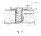
- FIG. 2Hillustrates a volume of a conductive compound 140 (e.g., the copper sulfide or another fill material) formed in the via 130 using the foregoing chemical process.
- the conductive compound 140can include at least one constituent from the plasma 151 ( FIG. 2G ), and at least one constituent from the side walls 131 of the via 130 .
- the conductive compound 140together with any other electrically conductive materials in the via 130 , can form an interconnect structure 160 .
- the interconnect structure 160has a first end 142 proximate to the bond site 122 , and a second end 143 toward the bottom of the via 130 .
- the conductive compound 140fills or at least approximately fills the remaining volume in the via 130 .
- the conductive compound 140can be used to fill only a portion of the via 130 .
- the workpiece 100can be further processed prior to coupling it to other components.
- the reaction mask 109 ( FIG. 2H ) and the resist layer 107 ( FIG. 2H )are removed (e.g., by a stripping process), as are the portions of the seed layer 134 and the barrier layer 133 that extend beyond the bond site 122 (e.g., using a wet chemistry etch and a dry plasma etch, respectively).
- a CMP processcan be used to flatten the surface (as will be described below with reference to FIG. 2K ), or the remaining conductive structures can form a stud, as shown in FIG. 2I .
- material from the second side 103 of the workpiece 100can be removed in a backgrinding process to expose the conductive material at the second end 143 of the interconnect structure 160 .
- a passivation layer 111can be added to the second side 103 of the workpiece 100 , and a bond pad 110 can be formed at the second end 143 of the interconnect structure 160 to facilitate bonding the workpiece 100 to other devices and/or structures.
- materialcan be removed from the second side 103 until the first conductive layer 137 is exposed.
- additional materialcan be removed to expose the second conductive layer 147 , the third conductive layer 148 , or the conductive compound 140 .
- FIG. 2Jillustrates the workpiece 100 after the reaction mask 109 ( FIG. 2I ) has been removed.
- conductive couplers 129e.g., solder balls or stud bumps
- conductive couplers 129are attached to the first end 142 , the second end 143 , or both ends of the interconnect structure 160 can depend on factors that include the characteristics of the workpiece 100 and/or the uses to which the workpiece 100 will be put. For example, if the workpiece 100 includes an imager die, it typically will include conductive couplers 129 at the second end 143 but not the first end 142 .
- the workpiece 100may include conductive couplers 129 at both the first and second ends 142 , 143 if it is to be placed in the middle of a stack of such dies, or at only one end if it is to be placed at the top or bottom of such a stack.
- the first end 142 of the interconnect structure 160can be further processed to expose the bond site 122 at the first end 142 . Accordingly, suitable etching, CMP, and/or other processes can be used to remove the materials (including a portion of the conductive compound 140 ) overlying the bond site 122 .
- Conductive couplers 126(shown as solder balls in FIG.
- 2Kare then attached to the workpiece 100 at the bond site 122 and the bond pad 110 to electrically connect the workpiece 100 to other workpieces (e.g., in a stacked arrangement), and/or to other components, for example, printed circuit boards, interposer boards, and/or any of a myriad of other suitable structures or devices.
- Embodiments of the process described above with reference to FIGS. 1A-2Kinclude disposing a conductive lining on the walls of a via 130 in a microfeature workpiece 100 , with opposing portions of the lining facing toward each other from opposing portions of the wall and bordering a space within the via.
- the methodcan further include chemically reacting the lining with a reactive material to form a chemical compound from a constituent of the reactive material and a constituent of the lining.
- the methodcan still further include at least partially filling the space with the chemical compound.
- the chemical reactionis between copper and sulfur hexafluoride and forms copper sulfide, though it can be between (or among) other constituents in other embodiments.
- the chemical reactionis expected to proceed quickly, which can reduce the amount of time required to form the conductive interconnect structure 160 in the workpiece 100 .
- the reactionis expected to proceed more quickly than the process of disposing a solder material in the via 130 , or plating material into the via 130 .
- the resulting microfeature workpiececan include a microfeature substrate having a via with opposing via wall portions, and a first conductive material disposed in a layer adjacent to the opposing wall portions.
- the workpiececan further include a second conductive material disposed adjacent to the first conductive material, with the second conductive material entirely filling a cross-sectional dimension of the via between opposing portions of the layer over at least part of a length of the via.
- the second conductive materialcan include a chemical compound that in turn includes a constituent of the layer.
- the first conductive materialcan include copper
- the second conductive materialcan include copper sulfide.
- neither of the conductive materialsincludes tin or lead or solder.
- the viacan be made to extend through less than an entire thickness of the workpiece (e.g., forming a blind via), and reacting the lining can include reacting the lining without first opening a vent hole at a blind end of the via opening.
- the vent holeis typically provided in the via to allow gases to escape from the via as liquid solder is disposed in the via. Because certain embodiments described above include a chemical reaction process rather than flowing liquid solder into the via, the need for a vent hole is eliminated. This not only eliminates the amount of time required to form the vent hole, but also eliminates the potential for damage to, and/or contamination of, the workpiece 101 which may result from forming the vent hole.
- the conductive compound 140is expected to be free or essentially free of voids. It is expected that the conductive compound 140 can form a more continuous electrical path in the interconnect structure 160 . The absence of voids can also reduce or eliminate the presence of gas molecules in the interconnect structure 160 , which might otherwise expand and potentially damage the interconnect structure 160 when the workpiece 100 undergoes subsequent processes at elevated temperatures.
- the formation of the chemical compound in the viacan be performed at relatively low temperatures.
- the workpiece 100can be exposed to a sulfur hexafluoride plasma at a temperature of about 60° C. This temperature may be varied and controlled to achieve a target reaction rate.
- Thisis unlike the process of filling the via 130 with solder, which requires an elevated temperature and which can accordingly use up a portion of the limited thermal budget associated with the workpiece 100 .
- workpieces 100 that include interconnect structures formed in the manners described aboveare expected to be more robust because the workpieces 100 may be exposed to fewer high temperature processes.
- soldertypically requires flux to remove surface oxides and provide for a good electrical and physical connection between the solder and the adjacent conductive structure.
- Embodiments of the chemical reactions described abovedo not require flux, and oxide removal can instead be performed by exposing the workpiece to a suitable plasma, prior to introducing the reactive material. This process is expected to be faster and/or more efficient than using a flux.
- the conductive compound 140can have a melting point higher than that of solder.
- CU 2 Shas a reported melting point of 1100° C.
- CuShas a reported decomposition temperature of about 220° C.
- Cu 2 Sis expected to have a decomposition temperature in the range of 327° C. to 527° C. when on platinum, and a decomposition temperature of about 677° C. when on ruthenium. Accordingly, when the temperature of the workpiece 100 is elevated during subsequent process step (e.g., reflow steps), the conductive compound 140 within the via 130 will not tend to reflow, melt, or otherwise change phase. As a result, the interconnect structure 160 is expected to be more physically and electrically robust than are many existing interconnect structures.
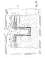
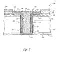
- FIG. 3illustrates a workpiece 300 having certain structures that differ from the workpiece 100 described above with reference to FIGS. 1A-2K .
- the workpiece 300can include an interconnect structure 360 having a different lateral extent than that of the interconnect structure 160 described above.
- the conductive material extending laterally away from the via 130e.g., in the conductive layers 137 , 147 , 148
- a reaction mask 309having larger openings than those of the reaction mask 109 ( FIG. 2G ) is positioned over the workpiece 100 .
- the conductive compound 140 formed in the chemical reactionalso extends laterally away from the via 130 .
- a solder ball or other conductive couplercan be attached directly to the laterally-extending conductive compound 140 , for example, if the conductivity of the conductive compound 140 is high enough. If it is not, the conductive compound 140 and other materials overlying the bond site 122 can be removed to expose the (generally more conductive) bond site 122 . Though not shown in FIG. 3 , the reaction mask 309 , and the resist layer 107 will be removed, as will those portions of the seed layer 134 and the barrier layer 133 that extend beyond the bond site 122 , as was discussed above with reference to FIG. 1I . As is also shown in FIG.
- more of the second surface 103 of the workpiece 300can be removed via a backgrinding process or other process than in the arrangement shown in FIG. 2K , to expose the conductive compound 140 within the via 130 .
- An appropriate bond pad 310can be formed at the exposed second end 143 of the interconnect structure 360 to prevent oxidation or another undesirable chemical reaction at the exposed second end 143 of the conductive compound 140 .
- the processing environment during the backgrinding processcan be controlled by the introduction of a suitable gas to prevent such reactions. In other embodiments, the backgrinding process can stop at other locations within the via (e.g., at the barrier layer 133 ).
- the processcan include other “sulfiding” reactions.
- other metalsNi, Sn, Co, Zn or Fe
- SF 6 plasmacan be reacted with an SF 6 plasma to form corresponding sulfides (NiS, SnS 2 , CoS, ZnS, or FeS/FeS 2 , respectively).
- other non-sulfiding reactionscan be used to form other suitable compounds.
- Suitable compoundsinclude borides, phosphides, and silicides.
- metals such as Ni or Fecan be exposed to a BF 3 or B 2 H 6 plasma to form Ni 2 B/Ni 3 B or FeB, respectively.
- metalscan be exposed to a PF 5 or PH 3 plasma to form FeP/Fe 2 P/Fe 3 P, Ni 2 P, Co 2 P or Zn 3 P 2 .
- a SiH 4 plasmacan be used to form Ni 2 Si/NiSi 2 , Cu 5 Si or CoSi 2 .
- the processescan include other reactions between conductive elements or compounds, and suitable reactive plasmas or other chemistries.
Landscapes
- Engineering & Computer Science (AREA)
- Computer Hardware Design (AREA)
- Microelectronics & Electronic Packaging (AREA)
- Power Engineering (AREA)
- Physics & Mathematics (AREA)
- Manufacturing & Machinery (AREA)
- Condensed Matter Physics & Semiconductors (AREA)
- General Physics & Mathematics (AREA)
- Plasma & Fusion (AREA)
- Internal Circuitry In Semiconductor Integrated Circuit Devices (AREA)
Abstract
Description
- The present disclosure is directed generally toward microfeature workpieces having conductive interconnect structures formed by chemically reactive processes, and associated systems and methods, including microfeature workpieces having conductive interconnect vias at least partially filled with copper sulfide.
- Microelectronic imagers are used in digital cameras, wireless devices with picture capabilities, and many other applications. Many cell phones and Personal Digital Assistants (PDAs), for example, incorporate microelectronic imagers for capturing and sending pictures. The growth rate of microelectronic imagers has been steadily increasing as they become smaller and produce better images with higher pixel counts.
- Microelectronic imagers include image sensors that use Charged Coupled Device (CCD) systems, Complementary Metal-Oxide Semiconductor (CMOS) systems, or other solid-state systems. CCD image sensors have been widely used in digital cameras and other applications. CMOS image sensors are also quickly becoming very popular because they are expected to have low production costs, high yields, and small sizes. CMOS image sensors can provide these advantages because they are manufactured using technology and equipment developed for fabricating semiconductor devices. CMOS image sensors, as well as CCD image sensors, are accordingly “packaged” to protect their delicate components and to provide external electrical contacts.
- Many imaging devices include semiconductor dies having image sensors located on a front surface of the die to receive incoming radiation. The dies also include bond pads for electrically coupling the sensors to other circuit elements. In order to prevent the bond pads from interfering with the operation of the sensors, or limiting the size and/or location of the sensors, the bond pads can be positioned on the opposite side of the die from the sensors (e.g., on the back surface of the die). Through-wafer interconnects (TWIs) are used to conduct electrical signals from the sensors and associated internal circuitry, through the die to the bond pads at the back surface. The TWIs are typically formed by making a blind via in the die, filling the via with solder, and then grinding the back surface of the die to expose the blind end of the via, which is used to form the bond pad. A solder ball can then be attached to the bond pad and can be reflowed to couple the die to external devices.
- One potential drawback associated with the foregoing approach is that, when the solder ball is later reflowed to electrically attach the die to external devices, the solder within the via may also tend to melt or at least soften. During the ensuing attach process, the solder within the via can be pulled at least partially out of the via, or can otherwise undergo deformations and/or movement that can adversely affect the electrical continuity of the TWI. In some instances, the electrical continuity of the TWI may be disrupted, causing the electrical connection between the image sensor and the external devices to fail.
- Another potential drawback associated with the foregoing approach is that the number of steps required to produce the TWI increases the cost of making the associated die. For example, the use of solder in the blind via requires forming a vent hole to allow gases within the via to escape as the solder enters. Even so, the solder may include voids, which can disrupt electrical continuity and in subsequent processes, expand and create electrical shorts. Still further, the processes required to dispose the solder in the via are typically high-temperature processes, which can use up a significant portion of the thermal budget of the die. Accordingly, there is a need for an improved process for forming microfeature workpiece electrical connections, including connections between dies and external devices.
FIG. 1A is a partially schematic illustration of a representative microfeature workpiece carrying microfeature dies configured in accordance with embodiments of the invention.FIG. 1B is a schematic illustration of a microfeature die singulated from the workpiece shown inFIG. 1A .FIG. 1C is a schematic illustration of a system which can include one or more microfeature dies in accordance with embodiments of the invention.FIG. 1D is a partially schematic, cross-sectional illustration of a portion of the workpiece prior to formation of a conductive structure in accordance with an embodiment of the invention.FIG. 1E is an enlarged view of a portion of the workpiece shown inFIG. 1A .FIGS. 2A-2K illustrate a process for introducing conductive material in a via by using a chemical reaction in accordance with an embodiment of the invention.FIG. 3 is an illustration of a substrate having features in accordance with another embodiment of the invention.- The following disclosure describes several embodiments of microfeature workpieces having conductive vias formed by chemically reactive processes, and associated systems and methods. Specific details of several embodiments of the invention are described below with reference to CMOS image sensors to provide a thorough understanding of these embodiments, but other embodiments can use CCD image sensors or other types of solid-state imaging devices. In still further embodiments, aspects of the invention can be practiced in connection with devices that do not include image sensors. Such devices include SRAM, DRAM, Flash, and other devices. In particular embodiments, the devices can be stacked on each other, and the vias can provide electrical communication among the stacked devices.
- As used herein, the terms “microfeature workpiece” and “workpiece” refer to substrates on and/in which microfeature electronic devices (including, but not limited to, image sensors) are integrally formed. A microfeature workpiece can include a wafer, and/or individual dies or combinations of dies that make up the wafer. Typical microfeature electronic devices of the workpiece include microfeature electronic circuits or components, thin-film recording heads, data storage elements, microfluidic devices and other products. Micromachines and micromechanical devices are included within this definition because they are manufactured using much of the same technology that is used in the fabrication of integrated circuits. The substrates can be semi-conductive pieces (e.g., doped silicon wafers or gallium arsenide wafers), non-conductive pieces (e.g., various ceramic substrates), or conductive pieces. In some cases, the workpieces are generally round, and in other cases the workpieces can have other shapes, including rectilinear shapes. Several embodiments of systems and methods for forming conductive structures in connection with microfeature workpiece fabrication are described below. A person skilled in the relevant art will understand, however, that the invention has additional embodiments, and that the invention may be practiced without several of the details of the embodiments described below with reference to
FIGS. 1A-3 . FIG. 1A is amicrofeature workpiece 100 in the form of awafer 170 that includes multiple microfeature dies120. At least some of the processes described below may be conducted on themicrofeature workpiece 100 at the wafer level, and other processes may be conducted on the individual microfeature dies120 of themicrofeature workpiece 100 after thedies 120 have been singulated from thelarger wafer 170. Accordingly, unless otherwise noted, structures and methods described below in the context of a “microfeature workpiece” can apply to thewafer 170 and/or thedies 120 that are formed from thewafer 170.FIG. 1B is a schematic illustration of anindividual die 120 after it has been singulated from thewafer 170 shown inFIG. 1A . The die120 can include operable microelectronic structure, optionally encased within a protective encapsulant. Pins, bond pads, solder balls, and/other conductive structures provide electrical communication between structures within the die120 and structures/devices located external to the die.- Individual dies may be incorporated into any of a myriad of larger and/or more
complex systems 180, a representative one of which is shown schematically inFIG. 1C . Thesystem 180 can include aprocessor 181, amemory 182, input/output devices 183, and/or other subsystems orcomponents 184. Microfeature workpieces (e.g., in the form of microfeature dies and/or combinations of microfeature dies) may be included in any of the components shown inFIG. 1C . The resultingsystem 180 can perform any of a wide variety of computing, processing, storage, sensor and/or other functions. Accordingly,representative systems 180 include, without limitation, computers and/or other data processors, for example, desktop computers, laptop computers, Internet appliances, hand-held devices (e.g., palm-top computers, wearable computers, cellular or mobile phones, multi-processor systems, processor-based or programmable consumer electronics, network computers, mini computers). Otherrepresentative systems 180 include cameras, light sensors, servers and associated server subsystems, display devices, and/or memory devices. Components of thesystem 180 may be housed in a single unit or distributed over multiple, interconnected units, e.g., through a communications network. Components can accordingly include local and/or remote memory storage devices, and any of a wide variety of computer-readable media, including magnetic or optically readable or removable computer disks. FIG. 1D is a side cross-sectional view of a portion of animager workpiece 100 prior to the formation of conductive interconnect structures in accordance with an embodiment of the invention. Theworkpiece 100 can include asubstrate 101 with a plurality of dies120 (e.g., imaging dies) formed in and/or on thesubstrate 101. Thesubstrate 101 has a first side orsurface 102 and a second side orsurface 103. Thesubstrate 101 can be a semiconductor wafer, with the dies120 arranged in a die pattern on the wafer. Individual dies120 can includeintegrated circuitry 121, a plurality of terminals or bond sites122 (e.g., bond pads) electrically coupled to theintegrated circuitry 121 withcouplers 126, and animage sensor 112. Theimage sensors 112 can be CMOS image sensors or CCD image sensors for capturing pictures or other images in the visible spectrum. In other embodiments, theimage sensors 112 can detect radiation in other spectrums (e.g., IR or UV ranges). Thebond sites 122 shown inFIG. 1D are external features at thefirst side 102 of thesubstrate 101. In other embodiments, however, thebond sites 122 can be internal features that are embedded at an intermediate depth within thesubstrate 101. First and seconddielectric layers first side 102 to protect theunderlying substrate 101.FIG. 1E is a side cross-sectional view of anarea 1E shown inFIG. 1D . This portion of theworkpiece 100 is representative of devices that include, but are not limited to, imager devices. Accordingly, the following discussion is also not limited to imager devices. Thesecond dielectric layer 105 has been patterned and etched to expose thebond site 122. Amask 106 is applied over thesecond dielectric layer 105 and patterned, as shown inFIG. 1E . Themask 106 can be a layer of resist that is patterned according to the arrangement ofbond sites 122 on thesubstrate 101. Accordingly, themask 106 can have an opening over eachbond site 122.- Referring next to
FIG. 2A , a via130 has been formed in theworkpiece 100 so as to extend into thesubstrate 101 through thebond site 122 and thefirst surface 102. The via130 can be formed using any of a variety of techniques, including etching or laser drilling. The via130 can be a blind via, as shown inFIG. 2A , e.g., a via that does not extend entirely through theworkpiece 100 and/or thesubstrate 101. In other embodiments, the via130 can extend entirely through theworkpiece 100 and/or thesubstrate 101, as indicated in dashed lines inFIG. 2A . Further details of representative methods for forming the via130 are disclosed in pending U.S. patent application Ser. No. 11/169,546, filed Jun. 28, 2005 and incorporated herein by reference. Athird dielectric layer 132 is deposited onto theworkpiece 100 to line thesidewalls 131 of the via130 within thesubstrate 101. The thirddielectric layer 132 electrically insulates components in thesubstrate 101 from an interconnect structure that is subsequently formed in thevia 130. - Referring to
FIG. 2B , a suitable etching process (e.g., a spacer etch) is used to remove portions of the thirddielectric layer 132 that extend over thebond site 122. Accordingly, at least part of thebond site 122 can be exposed for electrical coupling to conductive structures in the via130, as is described in greater detail below. - As shown in
FIG. 2C , aconductive barrier layer 133 is then deposited onto theworkpiece 100 over the thirddielectric layer 132 so as to be in electrical contact with thebond site 122. Thebarrier layer 133 generally covers thesecond dielectric layer 105 and thebond site 122 in addition to the thirddielectric layer 132. In one embodiment, for example, thebarrier layer 133 is a layer of tantalum that is deposited onto theworkpiece 100 using a physical vapor deposition (PVD) process. The thickness of thebarrier layer 133 is about 150 Angstroms. In other embodiments, thebarrier layer 133 may be deposited onto theworkpiece 100 using other vapor deposition processes, such as chemical vapor deposition (CVD), and/or may have a different thickness. The composition of thebarrier layer 133 is not limited to tantalum, but rather may be composed of tungsten or other suitable materials. - Referring next to
FIG. 2D , aseed layer 134 is deposited onto thebarrier layer 133. Theseed layer 134 can be deposited using vapor deposition techniques, such as PVD, CVD, atomic layer deposition, and/or plating. Theseed layer 134 can be composed of copper or other suitable materials. The thickness of theseed layer 134 may be about 2000 Angstroms, but can be more or less depending upon the depth and aspect ratio of thevia 130. In several embodiments, theseed layer 134 may not uniformly cover thebarrier layer 133, such that theseed layer 134 hasvoids 135 within thevia 130. This can cause non-uniform electroplating in the via130 and across theworkpiece 100. When theseed layer 134 is deficient, it may be enhanced using a process that fills voids or noncontinuous regions of theseed layer 134 to form a more uniform seed layer. Referring toFIG. 2E , for example, voids135 and/or noncontinuous regions of theseed layer 134 have been filled withadditional material 136, such as copper or another suitable material. One suitable seed layer enhancement process is described in U.S. Pat. No. 6,197,181, which is incorporated by reference. - Referring next to
FIG. 2F , a resistlayer 107 is deposited onto theseed layer 134 and is patterned to have anopening 108 over thebond site 122 and thevia 130. A first conductive lining orlayer 137 is then deposited onto the exposed portions of theseed layer 134 in thevia 130. The firstconductive layer 137 can include copper that is deposited onto theseed layer 134 in an electroless plating operation, or an electroplating operation, or by another suitable method. In the illustrated embodiment, the thickness of the firstconductive layer 137 is about 1 micron. In other embodiments, the firstconductive layer 137 may include other suitable materials and/or have a different thickness. A secondconductive layer 147 can then be deposited on the firstconductive layer 137. The secondconductive layer 147 can include nickel or another diffusion barrier that prevents or restricts migration of the material (e.g., copper) in the firstconductive layer 137. - A third
conductive layer 148 can then be disposed on the secondconductive layer 147. The thirdconductive layer 148 can also include copper. The combined thicknesses of the conductive layers is such that a space is located between opposing portions of the last-formed layer that face each other across the via130. - In particular embodiments, the third
conductive layer 148 is deliberately configured so as to withstand a loss of material during the formation of a conductive chemical compound in thevia 130. Accordingly, the thickness of the thirdconductive layer 148 can be selected based on how much material from the thirdconductive layer 148 is expected to be used up in the formation of the compound. The secondconductive layer 147 can act as a barrier to limit the loss of material to material from the thirdconductive layer 148, and prevent a loss of material from the firstconductive layer 137. Alternatively, the secondconductive layer 147 and the thirdconductive layer 148 can be eliminated, and the firstconductive layer 137 alone can be made thick enough to withstand the loss of material during the reaction process. Further details of an arrangement in which both the second andthird layers FIGS. 2H and 3 . However, it will be understood that aspects of the invention may also be practiced with just the firstconductive layer 137, provided it is thick enough. Further details of several embodiments for disposing the conductive layers in the via130 are disclosed in pending U.S. patent application Ser. No. 11/169,838, filed Jun. 28, 2005 and incorporated herein by reference. - In many existing processes, the open space in the via130 is filled with solder (e.g., a mixture of tin, silver and/or other constituents), while the solder is in a liquid state. Accordingly, a vent hole is formed between the bottom of the via130 and the
second side 103 of theworkpiece 101 to allow gases within the via130 to escape as the solder enters. In certain embodiments of the present invention, this step can be eliminated. Instead, as shown schematically inFIG. 2G , theworkpiece 100 can be placed in a reaction chamber150 (e.g., a plasma chamber) and exposed to a reactive material151 (e.g., a plasma). Thereactive material 151 chemically reacts with one or more of the conductive layers in the via130 to form a new chemical compound that fills or at least partially fills the via130. Areaction mask 109 can be positioned over the conductive material at the bond site122 (external to the via130) to protect this portion of the conductive material from exposure to thereactive material 151. Accordingly, thereaction mask 109 can have openings that are about the same size as the openings in the mask106 (FIG. 1B ) used to form thevias 130. - In a particular embodiment, the
reactive material 151 includes sulfur hexafluoride (SF6), which chemically reacts with copper in the thirdconductive layer 148 or, if the second and thirdconductive layers conductive layer 137. The reaction between the sulfur hexafluoride and the copper in the via130 forms enough copper sulfide (CuxSy) to fill the open cross-sectional space of the via130 over at least a portion of its length (and, in many embodiments, over the entire length of the space). The copper sulfide can include CuS, Cu2S, Cu9S5, and/or other chemical combinations of copper and sulfur atoms. The copper sulfide in the via130 may have a gradient of copper atoms, typically with more copper atoms toward the thirdconductive layer 148. For example, Cu2S may be present adjacent to the thirdconductive layer 148, and CuS may be present toward the center of thevia 130. - Controlling the amount of copper in the newly formed chemical compound can in turn control the stability of the compound. For example, the compound can have a chemical formula of CuxS, with x greater than or equal to one, and less than or equal to two. Higher values of x within this range are expected to produce more stable compounds. In at least some cases, the compound can be annealed for additional stability.
- In association with introducing the
reactive material 151, theworkpiece 100 can be exposed to a suitable reducing agent to remove copper oxides from the thirdconductive layer 148. For example, theworkpiece 100 can be exposed to a hydrogen-nitrogen plasma in a chemical etch process, or an argon plasma in a mechanical etch process. Removing the oxide exposes the more reactive copper below, and results in better physical and electrical contact between the pre-existing copper and the newly formed copper sulfide. The oxide can be removed before or simultaneously with exposing theworkpiece 100 to thereactive material 151. - Copper sulfide is a moderate conductor, and is generally less conductive than pure copper. Accordingly, if the dies formed from the
workpiece 101 require a higher conductivity in the via130 than is provided by copper sulfide, the process is performed so as to leave at least some copper in thevia 130. For example, if the thirdconductive layer 148 is not entirely consumed in the reaction with the sulfur hexafluoride, some copper will remain in the thirdconductive layer 148. If the entire thirdconductive layer 148 is consumed in the chemical reaction, then the secondconductive layer 147 can act as a stop layer and can accordingly preserve the copper in the firstconductive layer 137 to provide a relatively high conductivity link in thevia 130. In still another embodiment, in which the second and thirdconductive layers conductive layer 137 can exceed the amount copper consumed in the reaction that forms the copper sulfide so as to provide the relatively high conductivity link. On the other hand, if the copper sulfide alone provides sufficient conductivity in the via130 for the intended purposes of the resulting die, the entire amount of copper present at thewalls 131 of the via130 can be used up in the chemical reaction with the sulfur hexafluoride. FIG. 2H illustrates a volume of a conductive compound140 (e.g., the copper sulfide or another fill material) formed in the via130 using the foregoing chemical process. Accordingly, theconductive compound 140 can include at least one constituent from the plasma151 (FIG. 2G ), and at least one constituent from theside walls 131 of thevia 130. Theconductive compound 140, together with any other electrically conductive materials in the via130, can form aninterconnect structure 160. Theinterconnect structure 160 has afirst end 142 proximate to thebond site 122, and asecond end 143 toward the bottom of thevia 130. In an embodiment illustrated inFIG. 2H , theconductive compound 140 fills or at least approximately fills the remaining volume in thevia 130. In other embodiments, theconductive compound 140 can be used to fill only a portion of thevia 130.- After the
conductive compound 140 is formed in the via130, theworkpiece 100 can be further processed prior to coupling it to other components. For example, referring toFIG. 21 , the reaction mask109 (FIG. 2H ) and the resist layer107 (FIG. 2H ) are removed (e.g., by a stripping process), as are the portions of theseed layer 134 and thebarrier layer 133 that extend beyond the bond site122 (e.g., using a wet chemistry etch and a dry plasma etch, respectively). A CMP process can be used to flatten the surface (as will be described below with reference toFIG. 2K ), or the remaining conductive structures can form a stud, as shown inFIG. 2I . - As is also shown in
FIG. 2I , material from thesecond side 103 of theworkpiece 100 can be removed in a backgrinding process to expose the conductive material at thesecond end 143 of theinterconnect structure 160. Apassivation layer 111 can be added to thesecond side 103 of theworkpiece 100, and abond pad 110 can be formed at thesecond end 143 of theinterconnect structure 160 to facilitate bonding theworkpiece 100 to other devices and/or structures. In a particular aspect of this embodiment, material can be removed from thesecond side 103 until the firstconductive layer 137 is exposed. In other embodiments, additional material can be removed to expose the secondconductive layer 147, the thirdconductive layer 148, or theconductive compound 140. FIG. 2J illustrates theworkpiece 100 after the reaction mask109 (FIG. 2I ) has been removed. At this point, conductive couplers129 (e.g., solder balls or stud bumps) can be attached to theworkpiece 100 at thebond pad 110 and at thefirst end 142 of theinterconnect structure 160. Whetherconductive couplers 129 are attached to thefirst end 142, thesecond end 143, or both ends of theinterconnect structure 160 can depend on factors that include the characteristics of theworkpiece 100 and/or the uses to which theworkpiece 100 will be put. For example, if theworkpiece 100 includes an imager die, it typically will includeconductive couplers 129 at thesecond end 143 but not thefirst end 142. If theworkpiece 100 includes a DRAM die, it may includeconductive couplers 129 at both the first and second ends142,143 if it is to be placed in the middle of a stack of such dies, or at only one end if it is to be placed at the top or bottom of such a stack. In another arrangement, shown inFIG. 2K , thefirst end 142 of theinterconnect structure 160 can be further processed to expose thebond site 122 at thefirst end 142. Accordingly, suitable etching, CMP, and/or other processes can be used to remove the materials (including a portion of the conductive compound140) overlying thebond site 122. Conductive couplers126 (shown as solder balls inFIG. 2K ) are then attached to theworkpiece 100 at thebond site 122 and thebond pad 110 to electrically connect theworkpiece 100 to other workpieces (e.g., in a stacked arrangement), and/or to other components, for example, printed circuit boards, interposer boards, and/or any of a myriad of other suitable structures or devices.- Embodiments of the process described above with reference to
FIGS. 1A-2K include disposing a conductive lining on the walls of a via130 in amicrofeature workpiece 100, with opposing portions of the lining facing toward each other from opposing portions of the wall and bordering a space within the via. The method can further include chemically reacting the lining with a reactive material to form a chemical compound from a constituent of the reactive material and a constituent of the lining. The method can still further include at least partially filling the space with the chemical compound. In a particular embodiment, the chemical reaction is between copper and sulfur hexafluoride and forms copper sulfide, though it can be between (or among) other constituents in other embodiments. The chemical reaction is expected to proceed quickly, which can reduce the amount of time required to form theconductive interconnect structure 160 in theworkpiece 100. In particular, the reaction is expected to proceed more quickly than the process of disposing a solder material in the via130, or plating material into the via130. The resulting microfeature workpiece can include a microfeature substrate having a via with opposing via wall portions, and a first conductive material disposed in a layer adjacent to the opposing wall portions. The workpiece can further include a second conductive material disposed adjacent to the first conductive material, with the second conductive material entirely filling a cross-sectional dimension of the via between opposing portions of the layer over at least part of a length of the via. The second conductive material can include a chemical compound that in turn includes a constituent of the layer. For example, the first conductive material can include copper, and the second conductive material can include copper sulfide. In further particular aspects, neither of the conductive materials includes tin or lead or solder. - In particular embodiments, the via can be made to extend through less than an entire thickness of the workpiece (e.g., forming a blind via), and reacting the lining can include reacting the lining without first opening a vent hole at a blind end of the via opening. As discussed above, the vent hole is typically provided in the via to allow gases to escape from the via as liquid solder is disposed in the via. Because certain embodiments described above include a chemical reaction process rather than flowing liquid solder into the via, the need for a vent hole is eliminated. This not only eliminates the amount of time required to form the vent hole, but also eliminates the potential for damage to, and/or contamination of, the
workpiece 101 which may result from forming the vent hole. - In at least some of the embodiments described above, the
conductive compound 140 is expected to be free or essentially free of voids. It is expected that theconductive compound 140 can form a more continuous electrical path in theinterconnect structure 160. The absence of voids can also reduce or eliminate the presence of gas molecules in theinterconnect structure 160, which might otherwise expand and potentially damage theinterconnect structure 160 when theworkpiece 100 undergoes subsequent processes at elevated temperatures. - The formation of the chemical compound in the via can be performed at relatively low temperatures. For example, the
workpiece 100 can be exposed to a sulfur hexafluoride plasma at a temperature of about 60° C. This temperature may be varied and controlled to achieve a target reaction rate. This is unlike the process of filling the via130 with solder, which requires an elevated temperature and which can accordingly use up a portion of the limited thermal budget associated with theworkpiece 100. As a result,workpieces 100 that include interconnect structures formed in the manners described above are expected to be more robust because theworkpieces 100 may be exposed to fewer high temperature processes. Furthermore, solder typically requires flux to remove surface oxides and provide for a good electrical and physical connection between the solder and the adjacent conductive structure. Embodiments of the chemical reactions described above do not require flux, and oxide removal can instead be performed by exposing the workpiece to a suitable plasma, prior to introducing the reactive material. This process is expected to be faster and/or more efficient than using a flux. - Still further, the
conductive compound 140 can have a melting point higher than that of solder. For example, CU2S has a reported melting point of 1100° C. and CuS has a reported decomposition temperature of about 220° C. Cu2S is expected to have a decomposition temperature in the range of 327° C. to 527° C. when on platinum, and a decomposition temperature of about 677° C. when on ruthenium. Accordingly, when the temperature of theworkpiece 100 is elevated during subsequent process step (e.g., reflow steps), theconductive compound 140 within the via130 will not tend to reflow, melt, or otherwise change phase. As a result, theinterconnect structure 160 is expected to be more physically and electrically robust than are many existing interconnect structures. FIG. 3 illustrates aworkpiece 300 having certain structures that differ from theworkpiece 100 described above with reference toFIGS. 1A-2K . For example, theworkpiece 300 can include aninterconnect structure 360 having a different lateral extent than that of theinterconnect structure 160 described above. In a particular arrangement, the conductive material extending laterally away from the via130 (e.g., in theconductive layers reaction mask 309 having larger openings than those of the reaction mask109 (FIG. 2G ) is positioned over theworkpiece 100. Accordingly, theconductive compound 140 formed in the chemical reaction also extends laterally away from thevia 130. A solder ball or other conductive coupler can be attached directly to the laterally-extendingconductive compound 140, for example, if the conductivity of theconductive compound 140 is high enough. If it is not, theconductive compound 140 and other materials overlying thebond site 122 can be removed to expose the (generally more conductive)bond site 122. Though not shown inFIG. 3 , thereaction mask 309, and the resistlayer 107 will be removed, as will those portions of theseed layer 134 and thebarrier layer 133 that extend beyond thebond site 122, as was discussed above with reference toFIG. 1I . As is also shown inFIG. 3 , more of thesecond surface 103 of theworkpiece 300 can be removed via a backgrinding process or other process than in the arrangement shown inFIG. 2K , to expose theconductive compound 140 within thevia 130. Anappropriate bond pad 310 can be formed at the exposedsecond end 143 of theinterconnect structure 360 to prevent oxidation or another undesirable chemical reaction at the exposedsecond end 143 of theconductive compound 140. The processing environment during the backgrinding process can be controlled by the introduction of a suitable gas to prevent such reactions. In other embodiments, the backgrinding process can stop at other locations within the via (e.g., at the barrier layer133).- Particular embodiments of the foregoing processes were described in the context of a reaction between copper and sulfur hexafluoride to form a copper sulfide. In other embodiments, the process can include other “sulfiding” reactions. For example, other metals (Ni, Sn, Co, Zn or Fe) can be reacted with an SF6plasma to form corresponding sulfides (NiS, SnS2, CoS, ZnS, or FeS/FeS2, respectively). In further embodiments, other non-sulfiding reactions can be used to form other suitable compounds. Suitable compounds include borides, phosphides, and silicides. For example, metals such as Ni or Fe can be exposed to a BF3or B2H6plasma to form Ni2B/Ni3B or FeB, respectively. In still further embodiments, metals can be exposed to a PF5or PH3plasma to form FeP/Fe2P/Fe3P, Ni2P, Co2P or Zn3P2. A SiH4plasma can be used to form Ni2Si/NiSi2, Cu5Si or CoSi2. In still further embodiments, the processes can include other reactions between conductive elements or compounds, and suitable reactive plasmas or other chemistries.
- From the foregoing, it will be appreciated that specific embodiments of the invention have been described herein for purposes of illustration, but that various modifications may be made without deviating from the invention. For example, structures and/or processes described in the context of particular embodiments may be combined or eliminated in other embodiments. In particular, other embodiments can include other conductive compounds and/or conductive compounds formed from other constituents than those specifically described above. The connections between the interconnect structure and other devices (e.g., bond pads, conductive couplers and/or external devices) can have arrangements different than those described above. Accordingly, the invention is not limited except as by the appended claims.
Claims (68)
Priority Applications (3)
| Application Number | Priority Date | Filing Date | Title |
|---|---|---|---|
| US11/511,690US7629249B2 (en) | 2006-08-28 | 2006-08-28 | Microfeature workpieces having conductive interconnect structures formed by chemically reactive processes, and associated systems and methods |
| US12/624,215US7973411B2 (en) | 2006-08-28 | 2009-11-23 | Microfeature workpieces having conductive interconnect structures formed by chemically reactive processes, and associated systems and methods |
| US13/169,134US8610279B2 (en) | 2006-08-28 | 2011-06-27 | Microfeature workpieces having conductive interconnect structures formed by chemically reactive processes, and associated systems and methods |
Applications Claiming Priority (1)
| Application Number | Priority Date | Filing Date | Title |
|---|---|---|---|
| US11/511,690US7629249B2 (en) | 2006-08-28 | 2006-08-28 | Microfeature workpieces having conductive interconnect structures formed by chemically reactive processes, and associated systems and methods |
Related Child Applications (1)
| Application Number | Title | Priority Date | Filing Date |
|---|---|---|---|
| US12/624,215DivisionUS7973411B2 (en) | 2006-08-28 | 2009-11-23 | Microfeature workpieces having conductive interconnect structures formed by chemically reactive processes, and associated systems and methods |
Publications (2)
| Publication Number | Publication Date |
|---|---|
| US20080050911A1true US20080050911A1 (en) | 2008-02-28 |
| US7629249B2 US7629249B2 (en) | 2009-12-08 |
Family
ID=39197210
Family Applications (3)
| Application Number | Title | Priority Date | Filing Date |
|---|---|---|---|
| US11/511,690Active2027-12-05US7629249B2 (en) | 2006-08-28 | 2006-08-28 | Microfeature workpieces having conductive interconnect structures formed by chemically reactive processes, and associated systems and methods |
| US12/624,215Active2026-09-08US7973411B2 (en) | 2006-08-28 | 2009-11-23 | Microfeature workpieces having conductive interconnect structures formed by chemically reactive processes, and associated systems and methods |
| US13/169,134Active2027-08-03US8610279B2 (en) | 2006-08-28 | 2011-06-27 | Microfeature workpieces having conductive interconnect structures formed by chemically reactive processes, and associated systems and methods |
Family Applications After (2)
| Application Number | Title | Priority Date | Filing Date |
|---|---|---|---|
| US12/624,215Active2026-09-08US7973411B2 (en) | 2006-08-28 | 2009-11-23 | Microfeature workpieces having conductive interconnect structures formed by chemically reactive processes, and associated systems and methods |
| US13/169,134Active2027-08-03US8610279B2 (en) | 2006-08-28 | 2011-06-27 | Microfeature workpieces having conductive interconnect structures formed by chemically reactive processes, and associated systems and methods |
Country Status (1)
| Country | Link |
|---|---|
| US (3) | US7629249B2 (en) |
Cited By (28)
| Publication number | Priority date | Publication date | Assignee | Title |
|---|---|---|---|---|
| US20060042952A1 (en)* | 2004-08-24 | 2006-03-02 | Oliver Steven D | Methods for forming interconnects in vias and microelectronic workpieces including such interconnects |
| US20060216862A1 (en)* | 2003-11-13 | 2006-09-28 | Micron Technology, Inc. | Microelectronic devices, methods for forming vias in microelectronic devices, and methods for packaging microelectronic devices |
| US7435913B2 (en) | 2004-08-27 | 2008-10-14 | Micron Technology, Inc. | Slanted vias for electrical circuits on circuit boards and other substrates |
| US20080299759A1 (en)* | 2007-05-29 | 2008-12-04 | Freescale Semiconductor, Inc. | Method to form a via |
| US7589008B2 (en) | 2004-12-30 | 2009-09-15 | Micron Technology, Inc. | Methods for forming interconnects in microelectronic workpieces and microelectronic workpieces formed using such methods |
| US20090250821A1 (en)* | 2008-04-03 | 2009-10-08 | Micron Technologies, Inc. | Corrosion resistant via connections in semiconductor substrates and methods of making same |
| US7622377B2 (en) | 2005-09-01 | 2009-11-24 | Micron Technology, Inc. | Microfeature workpiece substrates having through-substrate vias, and associated methods of formation |
| US7683458B2 (en) | 2004-09-02 | 2010-03-23 | Micron Technology, Inc. | Through-wafer interconnects for photoimager and memory wafers |
| US7749899B2 (en) | 2006-06-01 | 2010-07-06 | Micron Technology, Inc. | Microelectronic workpieces and methods and systems for forming interconnects in microelectronic workpieces |
| US7791203B2 (en) | 2007-07-12 | 2010-09-07 | Micron Technology, Inc. | Interconnects for packaged semiconductor devices and methods for manufacturing such devices |
| US7795134B2 (en) | 2005-06-28 | 2010-09-14 | Micron Technology, Inc. | Conductive interconnect structures and formation methods using supercritical fluids |
| US20100264503A1 (en)* | 2009-04-16 | 2010-10-21 | Ikuko Inoue | Solid-state imaging device comprising through-electrode |
| US7829976B2 (en) | 2004-06-29 | 2010-11-09 | Micron Technology, Inc. | Microelectronic devices and methods for forming interconnects in microelectronic devices |
| US7830018B2 (en) | 2007-08-31 | 2010-11-09 | Micron Technology, Inc. | Partitioned through-layer via and associated systems and methods |
| US7863187B2 (en) | 2005-09-01 | 2011-01-04 | Micron Technology, Inc. | Microfeature workpieces and methods for forming interconnects in microfeature workpieces |
| US7884015B2 (en) | 2007-12-06 | 2011-02-08 | Micron Technology, Inc. | Methods for forming interconnects in microelectronic workpieces and microelectronic workpieces formed using such methods |
| US7902643B2 (en) | 2006-08-31 | 2011-03-08 | Micron Technology, Inc. | Microfeature workpieces having interconnects and conductive backplanes, and associated systems and methods |
| US7915736B2 (en) | 2005-09-01 | 2011-03-29 | Micron Technology, Inc. | Microfeature workpieces and methods for forming interconnects in microfeature workpieces |
| US7973411B2 (en) | 2006-08-28 | 2011-07-05 | Micron Technology, Inc. | Microfeature workpieces having conductive interconnect structures formed by chemically reactive processes, and associated systems and methods |
| US20110253440A1 (en)* | 2010-04-20 | 2011-10-20 | Nan Ya Pcb Corp. | Supporting substrate and method for fabricating the same |
| US8084866B2 (en) | 2003-12-10 | 2011-12-27 | Micron Technology, Inc. | Microelectronic devices and methods for filling vias in microelectronic devices |
| US8084854B2 (en) | 2007-12-28 | 2011-12-27 | Micron Technology, Inc. | Pass-through 3D interconnect for microelectronic dies and associated systems and methods |
| US8253230B2 (en) | 2008-05-15 | 2012-08-28 | Micron Technology, Inc. | Disabling electrical connections using pass-through 3D interconnects and associated systems and methods |
| US8536485B2 (en) | 2004-05-05 | 2013-09-17 | Micron Technology, Inc. | Systems and methods for forming apertures in microfeature workpieces |
| TWI415219B (en)* | 2009-12-01 | 2013-11-11 | Darrell Mcreynolds | Method of forming via interconnects for 3-d wafer/chip stacking |
| US20130313688A1 (en)* | 2012-05-25 | 2013-11-28 | Lapis Semiconductor Co., Ltd. | Semiconductor device and method of producing semiconductor device |
| JP2017011302A (en)* | 2016-10-04 | 2017-01-12 | ラピスセミコンダクタ株式会社 | Semiconductor device and manufacturing method thereof |
| JP2020198440A (en)* | 2018-11-29 | 2020-12-10 | ラピスセミコンダクタ株式会社 | Manufacturing method of semiconductor device |
Families Citing this family (22)
| Publication number | Priority date | Publication date | Assignee | Title |
|---|---|---|---|---|
| US8308053B2 (en) | 2005-08-31 | 2012-11-13 | Micron Technology, Inc. | Microfeature workpieces having alloyed conductive structures, and associated methods |
| KR101002680B1 (en) | 2008-10-21 | 2010-12-21 | 삼성전기주식회사 | Semiconductor package and manufacturing method thereof |
| US9406561B2 (en)* | 2009-04-20 | 2016-08-02 | International Business Machines Corporation | Three dimensional integrated circuit integration using dielectric bonding first and through via formation last |
| US8405201B2 (en)* | 2009-11-09 | 2013-03-26 | Taiwan Semiconductor Manufacturing Company, Ltd. | Through-silicon via structure |
| US8148257B1 (en)* | 2010-09-30 | 2012-04-03 | Infineon Technologies Ag | Semiconductor structure and method for making same |
| FR2965659B1 (en)* | 2010-10-05 | 2013-11-29 | Centre Nat Rech Scient | METHOD FOR MANUFACTURING AN INTEGRATED CIRCUIT |
| US8502340B2 (en) | 2010-12-09 | 2013-08-06 | Tessera, Inc. | High density three-dimensional integrated capacitors |
| US8742541B2 (en)* | 2010-12-09 | 2014-06-03 | Tessera, Inc. | High density three-dimensional integrated capacitors |
| KR101049380B1 (en)* | 2010-12-21 | 2011-07-15 | 한국기계연구원 | Through electrode for semiconductor device three-dimensional package using electroplating and manufacturing method thereof |
| US8487410B2 (en) | 2011-04-13 | 2013-07-16 | Taiwan Semiconductor Manufacturing Company, Ltd. | Through-silicon vias for semicondcutor substrate and method of manufacture |
| KR20130053338A (en) | 2011-11-15 | 2013-05-23 | 삼성전자주식회사 | Integrated circuit device having through silicon via structure |
| US8809191B2 (en)* | 2011-12-13 | 2014-08-19 | Stats Chippac, Ltd. | Semiconductor device and method of forming UBM structure on back surface of TSV semiconductor wafer |
| US8962469B2 (en)* | 2012-02-16 | 2015-02-24 | Infineon Technologies Ag | Methods of stripping resist after metal deposition |
| US8754531B2 (en)* | 2012-03-14 | 2014-06-17 | Nanya Technology Corp. | Through-silicon via with a non-continuous dielectric layer |
| US8563403B1 (en) | 2012-06-27 | 2013-10-22 | International Business Machines Corporation | Three dimensional integrated circuit integration using alignment via/dielectric bonding first and through via formation last |
| KR20140104778A (en)* | 2013-02-21 | 2014-08-29 | 삼성전자주식회사 | Methods for fabricating semiconductor devices having through vias |
| JP2015177382A (en)* | 2014-03-15 | 2015-10-05 | キヤノン株式会社 | Device with element electrode connected with through-wiring, and manufacturing method thereof |
| CN105870090B (en)* | 2015-01-20 | 2019-03-12 | 中芯国际集成电路制造(上海)有限公司 | Welding pad structure and production method |
| CN105118869B (en)* | 2015-09-21 | 2018-10-16 | 江苏多维科技有限公司 | A kind of 3 D stereo high-density film lamination capacitance and preparation method thereof |
| US9761509B2 (en)* | 2015-12-29 | 2017-09-12 | United Microelectronics Corp. | Semiconductor device with throgh-substrate via and method for fabrication the semiconductor device |
| US20180005887A1 (en)* | 2016-06-30 | 2018-01-04 | International Business Machines Corporation | Through-silicon via with injection molded fill |
| US10403591B2 (en)* | 2017-10-31 | 2019-09-03 | Xilinx, Inc. | Chip package assembly with enhanced interconnects and method for fabricating the same |
Citations (99)
| Publication number | Priority date | Publication date | Assignee | Title |
|---|---|---|---|---|
| US5857963A (en)* | 1996-07-17 | 1999-01-12 | Welch Allyn, Inc. | Tab imager assembly for use in an endoscope |
| US5861654A (en)* | 1995-11-28 | 1999-01-19 | Eastman Kodak Company | Image sensor assembly |
| US5893828A (en)* | 1996-05-02 | 1999-04-13 | Uram; Martin | Contact laser surgical endoscope and associated myringotomy procedure |
| US5904499A (en)* | 1994-12-22 | 1999-05-18 | Pace; Benedict G | Package for power semiconductor chips |
| US6171580B1 (en)* | 1997-11-18 | 2001-01-09 | Shiseido Company Ltd. | Ultraviolet-screening zinc oxide excellent in transparency and composition containing the same |
| US6184465B1 (en)* | 1998-11-12 | 2001-02-06 | Micron Technology, Inc. | Semiconductor package |
| US6187615B1 (en)* | 1998-08-28 | 2001-02-13 | Samsung Electronics Co., Ltd. | Chip scale packages and methods for manufacturing the chip scale packages at wafer level |
| US6191487B1 (en)* | 1998-04-23 | 2001-02-20 | Minco Technology Labs, Inc. | Semiconductor and flip chip packages and method having a back-side connection |
| US6222270B1 (en)* | 1997-06-24 | 2001-04-24 | Samsung Electronics Co., Ltd. | Integrated circuit bonding pads including closed vias and closed conductive patterns |
| US6228687B1 (en)* | 1999-06-28 | 2001-05-08 | Micron Technology, Inc. | Wafer-level package and methods of fabricating |
| US6229202B1 (en)* | 2000-01-10 | 2001-05-08 | Micron Technology, Inc. | Semiconductor package having downset leadframe for reducing package bow |
| US6235552B1 (en)* | 1999-07-09 | 2001-05-22 | Samsung Electronics Co., Ltd. | Chip scale package and method for manufacturing the same using a redistribution substrate |
| US6341009B1 (en)* | 2000-02-24 | 2002-01-22 | Quantronix Corporation | Laser delivery system and method for photolithographic mask repair |
| US6344976B1 (en)* | 1997-04-07 | 2002-02-05 | Micron Technology, Inc. | Interdigitated leads-over-chip lead frame device and method for supporting an integrated circuit die |
| US6359328B1 (en)* | 1998-12-31 | 2002-03-19 | Intel Corporation | Methods for making interconnects and diffusion barriers in integrated circuits |
| US6372548B2 (en)* | 1998-06-04 | 2002-04-16 | Matsushita Electric Industrial Co., Ltd. | Method for fabricating a semiconductor package with a semiconductor device attached to a multilayered substrate |
| US6391770B2 (en)* | 1997-04-24 | 2002-05-21 | Mitsubishi Denki Kabushiki Kaisha | Method of manufacturing semiconductor device |
| US6534863B2 (en)* | 2001-02-09 | 2003-03-18 | International Business Machines Corporation | Common ball-limiting metallurgy for I/O sites |
| US6545563B1 (en)* | 1990-07-16 | 2003-04-08 | Raytheon Company | Digitally controlled monolithic microwave integrated circuits |
| US6555782B2 (en)* | 1997-12-12 | 2003-04-29 | Matsushita Electric Industrial Co., Ltd. | Laser machining method, laser machining apparatus, and its control method |
| US6560047B2 (en)* | 2001-08-29 | 2003-05-06 | Samsung Electro-Mechanics Co., Ltd. | Image module |
| US6569711B1 (en)* | 1998-04-28 | 2003-05-27 | International Business Machines Corporation | Methods and apparatus for balancing differences in thermal expansion in electronic packaging |
| US6569777B1 (en)* | 2002-10-02 | 2003-05-27 | Taiwan Semiconductor Manufacturing Co., Ltd | Plasma etching method to form dual damascene with improved via profile |
| US6680459B2 (en)* | 2001-06-22 | 2004-01-20 | Nippei Toyama Corporation | Laser beam machining apparatus and laser beam machining method |
| US6699787B2 (en)* | 2001-06-14 | 2004-03-02 | Shinko Electric Industries Co., Ltd. | Semiconductor device and method of production of same |
| US6703310B2 (en)* | 2001-06-14 | 2004-03-09 | Shinko Electric Industries Co., Ltd. | Semiconductor device and method of production of same |
| US6838377B2 (en)* | 2001-03-05 | 2005-01-04 | Murata Manufacturing Co., Ltd. | High frequency circuit chip and method of producing the same |
| US6856023B2 (en)* | 2002-01-22 | 2005-02-15 | Canon Kabushiki Kaisha | Semiconductor device and method of manufacturing semiconductor device |
| US6873054B2 (en)* | 2002-04-24 | 2005-03-29 | Seiko Epson Corporation | Semiconductor device and a method of manufacturing the same, a circuit board and an electronic apparatus |
| US6885107B2 (en)* | 2002-08-29 | 2005-04-26 | Micron Technology, Inc. | Flip-chip image sensor packages and methods of fabrication |
| US6982487B2 (en)* | 2003-03-25 | 2006-01-03 | Samsung Electronics Co., Ltd. | Wafer level package and multi-package stack |
| US20060014313A1 (en)* | 2004-07-16 | 2006-01-19 | Hall Frank L | Microelectronic imaging units and methods of manufacturing microelectronic imaging units |
| US20060011809A1 (en)* | 2004-07-19 | 2006-01-19 | Farnworth Warren M | Microelectronic imagers with optical devices and methods of manufacturing such microelectronic imagers |
| US20060024856A1 (en)* | 2004-07-28 | 2006-02-02 | Derderian James M | Microelectronic imaging units and methods of manufacturing microelectronic imaging units |
| US20060023107A1 (en)* | 2004-08-02 | 2006-02-02 | Bolken Todd O | Microelectronic imagers with optics supports having threadless interfaces and methods for manufacturing such microelectronic imagers |
| US20060035415A1 (en)* | 2004-08-16 | 2006-02-16 | Wood Alan G | Frame structure and semiconductor attach process for use therewith for fabrication of image sensor packages and the like, and resulting packages |
| US20060035402A1 (en)* | 2004-08-10 | 2006-02-16 | Street Bret K | Microelectronic imaging units and methods of manufacturing microelectronic imaging units |
| US20060038183A1 (en)* | 2004-08-19 | 2006-02-23 | Oliver Steven D | Microelectronic imagers with curved image sensors and methods for manufacturing microelectronic imagers |
| US20060038272A1 (en)* | 2004-08-17 | 2006-02-23 | Texas Instruments Incorporated | Stacked wafer scale package |
| US20060040428A1 (en)* | 2004-08-19 | 2006-02-23 | Johnson Mark S | Conductive structures for microfeature devices and methods for fabricating microfeature devices |
| US20060040421A1 (en)* | 2004-08-19 | 2006-02-23 | Farnworth Warren M | Spacers for packaged microelectronic imagers and methods of making and using spacers for wafer-level packaging of imagers |
| US20060043599A1 (en)* | 2004-09-02 | 2006-03-02 | Salman Akram | Through-wafer interconnects for photoimager and memory wafers |
| US20060044433A1 (en)* | 2004-08-31 | 2006-03-02 | Micron Technology, Inc. | Microelectronic imagers having front side contacts and methods of packaging such microelectronic imagers |
| US20060043509A1 (en)* | 2004-08-24 | 2006-03-02 | Watkins Charles M | Packaged microelectronic imaging devices and methods of packaging microelectronic imaging devices |
| US20060042952A1 (en)* | 2004-08-24 | 2006-03-02 | Oliver Steven D | Methods for forming interconnects in vias and microelectronic workpieces including such interconnects |
| US20060046537A1 (en)* | 2004-08-27 | 2006-03-02 | Chong Chin H | Slanted vias for electrical circuits on circuit boards and other substrates |
| US20060043262A1 (en)* | 2004-08-30 | 2006-03-02 | Micron Technology, Inc. | Microelectronic imagers with integrated optical devices and methods for manufacturing such microelectronic imagers |
| US20060046471A1 (en)* | 2004-08-27 | 2006-03-02 | Kirby Kyle K | Methods for forming vias of varying lateral dimensions and semiconductor components and assemblies including same |
| US20060043512A1 (en)* | 2004-08-24 | 2006-03-02 | Oliver Steven D | Microelectronic imagers with optical devices having integral reference features and methods for manufacturing such microelectronic imagers |
| US20060046468A1 (en)* | 2004-08-31 | 2006-03-02 | Salman Akram | Through-substrate interconnect fabrication methods and resulting structures and assemblies |
| US20060043569A1 (en)* | 2004-08-27 | 2006-03-02 | Benson Peter A | Low temperature methods of forming back side redistribution layers in association with through wafer interconnects, semiconductor devices including same, and assemblies |
| US20060046332A1 (en)* | 2004-08-26 | 2006-03-02 | Derderian James M | Microelectronic Imaging units and methods of manufacturing microelectronic imaging units |
| US20060057776A1 (en)* | 2004-09-10 | 2006-03-16 | Advanced Semiconductor Engineering Inc. | Wafer stacking package method |
| US20060057836A1 (en)* | 2004-09-10 | 2006-03-16 | Agency For Science, Technology And Research | Method of stacking thin substrates by transfer bonding |
| US7022609B2 (en)* | 2002-08-30 | 2006-04-04 | Fujikura Ltd. | Manufacturing method of a semiconductor substrate provided with a through hole electrode |
| US7023090B2 (en)* | 2003-01-29 | 2006-04-04 | Taiwan Semiconductor Manufacturing Company, Ltd. | Bonding pad and via structure design |
| US7029937B2 (en)* | 2002-03-19 | 2006-04-18 | Seiko Epson Corporation | Semiconductor device and method of manufacturing the same, circuit board, and electronic instrument |
| US7033927B2 (en)* | 2004-06-22 | 2006-04-25 | International Business Machines Corporation | Apparatus and method for thermal isolation, circuit cooling and electromagnetic shielding of a wafer |
| US7037836B2 (en)* | 2002-12-16 | 2006-05-02 | Dongbuanam Semiconductor Inc. | Method of manufacturing a semiconductor device without oxidized copper layer |
| US7041598B2 (en)* | 2003-06-25 | 2006-05-09 | Hewlett-Packard Development Company, L.P. | Directional ion etching process for patterning self-aligned via contacts |
| US7045015B2 (en)* | 1998-09-30 | 2006-05-16 | Optomec Design Company | Apparatuses and method for maskless mesoscale material deposition |
| US20070004079A1 (en)* | 2005-06-30 | 2007-01-04 | Geefay Frank S | Method for making contact through via contact to an offset contactor inside a cap for the wafer level packaging of FBAR chips |
| US7164565B2 (en)* | 2002-11-29 | 2007-01-16 | Sigmatel, Inc. | ESD protection circuit |
| US20070012655A1 (en)* | 2005-07-15 | 2007-01-18 | Samsung Electronics Co., Ltd. | Micro-package, multi-stack micro-package, and manufacturing method therefor |
| US7166247B2 (en)* | 2002-06-24 | 2007-01-23 | Micron Technology, Inc. | Foamed mechanical planarization pads made with supercritical fluid |
| US20070020805A1 (en)* | 2002-02-20 | 2007-01-25 | Kim Sarah E | Etch stop layer for silicon (Si) via etch in three-dimensional (3-D) wafer-to-wafer vertical stack |
| US20070020935A1 (en)* | 2005-07-19 | 2007-01-25 | Taylor Theodore M | Process for enhancing solubility and reaction rates in supercritical fluids |
| US7170183B1 (en)* | 2005-05-13 | 2007-01-30 | Amkor Technology, Inc. | Wafer level stacked package |
| US20070023121A1 (en)* | 2005-07-29 | 2007-02-01 | Freescale Semiconductor, Inc. | Fabrication of three dimensional integrated circuit employing multiple die panels |
| US20070032061A1 (en)* | 2005-08-05 | 2007-02-08 | Farnworth Warren M | Methods of forming through-wafer interconnects and structures resulting therefrom |
| US20070037379A1 (en)* | 2005-08-11 | 2007-02-15 | Ziptronix | 3D IC method and device |
| US20070035033A1 (en)* | 2005-05-26 | 2007-02-15 | Volkan Ozguz | Stackable tier structure comprising high density feedthrough |
| US20070042598A1 (en)* | 2003-03-04 | 2007-02-22 | Hyun-Mog Park | Dielectric with sidewall passivating layer |
| US7183653B2 (en)* | 2003-12-17 | 2007-02-27 | Intel Corporation | Via including multiple electrical paths |
| US7183176B2 (en)* | 2004-08-25 | 2007-02-27 | Agency For Science, Technology And Research | Method of forming through-wafer interconnects for vertical wafer level packaging |
| US20070045779A1 (en)* | 2005-09-01 | 2007-03-01 | Hiatt W M | Methods for forming through-wafer interconnects, intermediate structures so formed, and devices and systems having at least one solder dam structure |
| US20070045834A1 (en)* | 2005-08-31 | 2007-03-01 | Micron Technology, Inc. | Interconnecting substrates for microelectronic dies, methods for forming vias in such substrates, and methods for packaging microelectronic devices |
| US20070045826A1 (en)* | 2005-09-01 | 2007-03-01 | Micron Technology, Inc. | Microfeature workpiece substrates having through-substrate vias, and associated methods of formation |
| US20070045515A1 (en)* | 2005-09-01 | 2007-03-01 | Micron Technology, Inc. | Microelectronic imaging devices and associated methods for attaching transmissive elements |
| US20070048896A1 (en)* | 2005-08-30 | 2007-03-01 | International Business Machines Corporation | Conductive through via structure and process for electronic device carriers |
| US20070045388A1 (en)* | 2005-08-31 | 2007-03-01 | Micron Technology, Inc. | Microfeature workpieces having alloyed conductive structures, and associated methods |
| US20070045632A1 (en)* | 2005-09-01 | 2007-03-01 | Micron Technology, Inc. | Microelectronic imaging units and methods of manufacturing microelectronic imaging units at the wafer level |
| US20070045812A1 (en)* | 2005-08-31 | 2007-03-01 | Micron Technology, Inc. | Microfeature assemblies including interconnect structures and methods for forming such interconnect structures |
| US20070048994A1 (en)* | 2005-09-01 | 2007-03-01 | Tuttle Mark E | Methods for forming through-wafer interconnects and structures resulting therefrom |
| US20070045120A1 (en)* | 2005-09-01 | 2007-03-01 | Micron Technology, Inc. | Methods and apparatus for filling features in microfeature workpieces |
| US20070045806A1 (en)* | 2004-02-05 | 2007-03-01 | United Microelectronics Corp. | Structure of an ultra-thin wafer level stack package |
| US20070049019A1 (en)* | 2005-09-01 | 2007-03-01 | Wai Chien M | Method of selectively depositing materials on a substrate using a supercritical fluid |
| US20070049016A1 (en)* | 2005-09-01 | 2007-03-01 | Micron Technology, Inc. | Microfeature workpieces and methods for forming interconnects in microfeature workpieces |
| US7186650B1 (en)* | 2004-08-02 | 2007-03-06 | Advanced Micro Devices, Inc. | Control of bottom dimension of tapered contact via variation(s) of etch process |
| US7190061B2 (en)* | 2003-01-03 | 2007-03-13 | Samsung Electronics Co., Ltd. | stack package made of chip scale packages |
| US20070057028A1 (en)* | 2005-08-30 | 2007-03-15 | Micron Technology, Inc. | Systems and methods for depositing conductive material into openings in microfeature workpieces |
| US7199050B2 (en)* | 2004-08-24 | 2007-04-03 | Micron Technology, Inc. | Pass through via technology for use during the manufacture of a semiconductor device |
| US20070077753A1 (en)* | 2004-09-09 | 2007-04-05 | Iwatake Michael M | Fabrication of via contacts having dual silicide layers |
| US20070082427A1 (en)* | 2005-10-12 | 2007-04-12 | Mitsubishi Electric Corporation | Method for manufacturing a compound semiconductor device having an improved via hole |
| US20070096263A1 (en)* | 2005-11-03 | 2007-05-03 | International Business Machines Corporation | Accessible chip stack and process of manufacturing thereof |
| US20070099395A1 (en)* | 2005-11-03 | 2007-05-03 | Uppili Sridhar | Wafer level packaging process |
| US7217596B2 (en)* | 2002-05-08 | 2007-05-15 | Micron Technology, Inc. | Stacked die module and techniques for forming a stacked die module |
| US20080054444A1 (en)* | 2006-08-31 | 2008-03-06 | Micron Technology, Inc. | Microfeature workpieces having interconnects and conductive backplanes, and associated systems and methods |
| US20080057620A1 (en)* | 2006-08-30 | 2008-03-06 | Micron Technology, Inc. | Redistribution layers for microfeature workpieces, and associated systems and methods |
Family Cites Families (364)
| Publication number | Priority date | Publication date | Assignee | Title |
|---|---|---|---|---|
| US2821959A (en) | 1956-03-29 | 1958-02-04 | Bell Telephone Labor Inc | Mass soldering of electrical assemblies |
| US3006318A (en) | 1958-03-26 | 1961-10-31 | Western Electric Co | Apparatus for applying solder coatings to surfaces |
| DE1160831B (en) | 1962-04-21 | 1964-01-09 | Knapsack Ag | Method and device for the production of titanium nitride |
| US3865298A (en) | 1973-08-14 | 1975-02-11 | Atomic Energy Commission | Solder leveling |
| US3902036A (en) | 1974-05-02 | 1975-08-26 | Western Electric Co | Control system using multiplexed laser beams |
| US4040168A (en) | 1975-11-24 | 1977-08-09 | Rca Corporation | Fabrication method for a dual gate field-effect transistor |
| US4368106A (en) | 1980-10-27 | 1983-01-11 | General Electric Company | Implantation of electrical feed-through conductors |
| US5027184A (en) | 1981-03-02 | 1991-06-25 | Rockwell International Corporation | NPN type lateral transistor with minimal substrate operation interference |
| NZ201877A (en) | 1981-09-24 | 1985-02-28 | R E Mcintyre | Electrical connector:plug rotation livens socket contacts |
| US4756765A (en) | 1982-01-26 | 1988-07-12 | Avco Research Laboratory, Inc. | Laser removal of poor thermally-conductive materials |
| US4534100A (en) | 1982-06-28 | 1985-08-13 | The United States Of America As Represented By The Secretary Of The Air Force | Electrical method of making conductive paths in silicon |
| GB8312850D0 (en) | 1983-05-10 | 1983-06-15 | British Telecomm | Semiconductor wafer fabrication |
| JPS60220940A (en) | 1983-05-20 | 1985-11-05 | Hitachi Ltd | Foreign matter automatic inspection device |
| FR2547519B1 (en) | 1983-06-15 | 1987-07-03 | Snecma | LASER DRILLING METHOD AND DEVICE |
| US4581301A (en) | 1984-04-10 | 1986-04-08 | Michaelson Henry W | Additive adhesive based process for the manufacture of printed circuit boards |
| US4984597B1 (en) | 1984-05-21 | 1999-10-26 | Cfmt Inc | Apparatus for rinsing and drying surfaces |
| US4660063A (en) | 1985-03-18 | 1987-04-21 | General Electric Company | Immersion type ISFET |
| US4627971A (en) | 1985-04-22 | 1986-12-09 | Alza Corporation | Osmotic device with self-sealing passageway |
| US5026964A (en) | 1986-02-28 | 1991-06-25 | General Electric Company | Optical breakthrough sensor for laser drill |
| JPH07112041B2 (en) | 1986-12-03 | 1995-11-29 | シャープ株式会社 | Method for manufacturing semiconductor device |
| US4768291A (en) | 1987-03-12 | 1988-09-06 | Monarch Technologies Corporation | Apparatus for dry processing a semiconductor wafer |
| US4907127A (en) | 1988-03-21 | 1990-03-06 | Lee John K C | Printed circuit board construction and method for producing printed circuit end products |
| US5219344A (en) | 1988-06-09 | 1993-06-15 | Visx, Incorporated | Methods and apparatus for laser sculpture of the cornea |
| DE3831141A1 (en) | 1988-09-13 | 1990-03-22 | Zeiss Carl Fa | METHOD AND DEVICE FOR MICROSURGERY ON EYE BY LASER RADIATION |
| FR2637151A1 (en) | 1988-09-29 | 1990-03-30 | Commissariat Energie Atomique | METHOD OF MAKING ELECTRICAL CONNECTIONS THROUGH A SUBSTRATE |
| US4959705A (en) | 1988-10-17 | 1990-09-25 | Ford Microelectronics, Inc. | Three metal personalization of application specific monolithic microwave integrated circuit |
| US5024966A (en) | 1988-12-21 | 1991-06-18 | At&T Bell Laboratories | Method of forming a silicon-based semiconductor optical device mount |
| JPH02235589A (en) | 1989-03-09 | 1990-09-18 | Fuji Electric Co Ltd | Laser beam machining method |
| JPH02257643A (en) | 1989-03-29 | 1990-10-18 | Mitsubishi Electric Corp | Semiconductor device and its manufacturing method |
| US5347149A (en) | 1989-11-29 | 1994-09-13 | Texas Instruments Incorporated | Integrated circuit and method |
| US5145099A (en) | 1990-07-13 | 1992-09-08 | Micron Technology, Inc. | Method for combining die attach and lead bond in the assembly of a semiconductor package |
| FR2665574B1 (en) | 1990-08-03 | 1997-05-30 | Thomson Composants Microondes | METHOD FOR INTERCONNECTING BETWEEN AN INTEGRATED CIRCUIT AND A SUPPORT CIRCUIT, AND INTEGRATED CIRCUIT SUITABLE FOR THIS METHOD. |
| JP2797684B2 (en) | 1990-10-04 | 1998-09-17 | ブラザー工業株式会社 | Nozzle manufacturing method and manufacturing apparatus |
| US5294568A (en) | 1990-10-12 | 1994-03-15 | Genus, Inc. | Method of selective etching native oxide |
| US5292686A (en) | 1991-08-21 | 1994-03-08 | Triquint Semiconductor, Inc. | Method of forming substrate vias in a GaAs wafer |
| US5289631A (en) | 1992-03-04 | 1994-03-01 | Mcnc | Method for testing, burn-in, and/or programming of integrated circuit chips |
| JPH05251717A (en) | 1992-03-04 | 1993-09-28 | Hitachi Ltd | Semiconductor package and semiconductor module |
| US5389738A (en) | 1992-05-04 | 1995-02-14 | Motorola, Inc. | Tamperproof arrangement for an integrated circuit device |
| US5233448A (en) | 1992-05-04 | 1993-08-03 | Industrial Technology Research Institute | Method of manufacturing a liquid crystal display panel including photoconductive electrostatic protection |
| US5304743A (en) | 1992-05-12 | 1994-04-19 | Lsi Logic Corporation | Multilayer IC semiconductor package |
| US5384717A (en) | 1992-11-23 | 1995-01-24 | Ford Motor Company | Non-contact method of obtaining dimensional information about an object |
| US5464960A (en) | 1993-01-12 | 1995-11-07 | Iatrotech, Inc. | Laser calibration device |
| CA2154357C (en) | 1993-02-04 | 2004-03-02 | Kevin A. Shaw | Microstructures and single-mask, single-crystal process for fabrication thereof |
| JPH06310547A (en) | 1993-02-25 | 1994-11-04 | Mitsubishi Electric Corp | Semiconductor device and manufacture thereof |
| JP2842132B2 (en) | 1993-03-05 | 1998-12-24 | 松下電器産業株式会社 | Optical device |
| US5447871A (en) | 1993-03-05 | 1995-09-05 | Goldstein; Edward F. | Electrically conductive interconnection through a body of semiconductor material |
| JPH06268020A (en) | 1993-03-10 | 1994-09-22 | Sumitomo Electric Ind Ltd | Semiconductor device |
| US5480835A (en) | 1993-05-06 | 1996-01-02 | Motorola, Inc. | Electrical interconnect and method for forming the same |
| CO4230054A1 (en) | 1993-05-07 | 1995-10-19 | Visx Inc | METHOD AND SYSTEMS FOR LASER TREATMENT OF REFRACTIVE ERRORS USING TRAVELING IMAGES FORMATION |
| NL9300971A (en) | 1993-06-04 | 1995-01-02 | Framatome Connectors Belgium | Circuit board connector assembly. |
| US5518956A (en) | 1993-09-02 | 1996-05-21 | General Electric Company | Method of isolating vertical shorts in an electronic array using laser ablation |
| US5378312A (en) | 1993-12-07 | 1995-01-03 | International Business Machines Corporation | Process for fabricating a semiconductor structure having sidewalls |
| SE9304145D0 (en) | 1993-12-10 | 1993-12-10 | Pharmacia Lkb Biotech | Ways to manufacture cavity structures |
| US5378313A (en) | 1993-12-22 | 1995-01-03 | Pace; Benedict G. | Hybrid circuits and a method of manufacture |
| US5585308A (en) | 1993-12-23 | 1996-12-17 | Sgs-Thomson Microelectronics, Inc. | Method for improved pre-metal planarization |
| JP3531199B2 (en) | 1994-02-22 | 2004-05-24 | 三菱電機株式会社 | Optical transmission equipment |
| US5380681A (en) | 1994-03-21 | 1995-01-10 | United Microelectronics Corporation | Three-dimensional multichip package and methods of fabricating |
| US6008914A (en) | 1994-04-28 | 1999-12-28 | Mitsubishi Denki Kabushiki Kaisha | Laser transfer machining apparatus |
| US5470787A (en) | 1994-05-02 | 1995-11-28 | Motorola, Inc. | Semiconductor device solder bump having intrinsic potential for forming an extended eutectic region and method for making and using the same |
| US5627106A (en) | 1994-05-06 | 1997-05-06 | United Microelectronics Corporation | Trench method for three dimensional chip connecting during IC fabrication |
| US5585675A (en) | 1994-05-11 | 1996-12-17 | Harris Corporation | Semiconductor die packaging tub having angularly offset pad-to-pad via structure configured to allow three-dimensional stacking and electrical interconnections among multiple identical tubs |
| JPH07335783A (en) | 1994-06-13 | 1995-12-22 | Fujitsu Ltd | Semiconductor device and semiconductor device unit |
| JPH0897375A (en) | 1994-07-26 | 1996-04-12 | Toshiba Corp | Microwave integrated circuit device and manufacturing method thereof |
| US5515167A (en) | 1994-09-13 | 1996-05-07 | Hughes Aircraft Company | Transparent optical chuck incorporating optical monitoring |
| US5521434A (en) | 1994-10-17 | 1996-05-28 | International Business Machines Corporation | Semiconductor chip and electronic module with integrated surface interconnects/components |
| JPH08167630A (en) | 1994-12-15 | 1996-06-25 | Hitachi Ltd | Chip connection structure |
| US5624437A (en) | 1995-03-28 | 1997-04-29 | Freeman; Jerre M. | High resolution, high speed, programmable laser beam modulating apparatus for microsurgery |
| US5814889A (en) | 1995-06-05 | 1998-09-29 | Harris Corporation | Intergrated circuit with coaxial isolation and method |
| US5646067A (en) | 1995-06-05 | 1997-07-08 | Harris Corporation | Method of bonding wafers having vias including conductive material |
| US5618752A (en) | 1995-06-05 | 1997-04-08 | Harris Corporation | Method of fabrication of surface mountable integrated circuits |
| US5718791A (en) | 1995-06-05 | 1998-02-17 | R + S Stanztechnik Gmbh | Method of laminating a trim panel and folding a cover sheet edge around the panel rim |
| US6195883B1 (en) | 1998-03-25 | 2001-03-06 | International Business Machines Corporation | Full additive process with filled plated through holes |
| US5874780A (en) | 1995-07-27 | 1999-02-23 | Nec Corporation | Method of mounting a semiconductor device to a substrate and a mounted structure |
| US5673846A (en) | 1995-08-24 | 1997-10-07 | International Business Machines Corporation | Solder anchor decal and method |
| JP3263705B2 (en) | 1995-09-21 | 2002-03-11 | 三菱電機株式会社 | Printed wiring board and flat panel display driving circuit printed wiring board and flat panel display device |
| JP2905736B2 (en) | 1995-12-18 | 1999-06-14 | 株式会社エイ・ティ・アール光電波通信研究所 | Semiconductor device |
| US5851845A (en) | 1995-12-18 | 1998-12-22 | Micron Technology, Inc. | Process for packaging a semiconductor die using dicing and testing |
| US5776824A (en) | 1995-12-22 | 1998-07-07 | Micron Technology, Inc. | Method for producing laminated film/metal structures for known good die ("KG") applications |
| US5773359A (en) | 1995-12-26 | 1998-06-30 | Motorola, Inc. | Interconnect system and method of fabrication |
| US5673730A (en) | 1996-01-24 | 1997-10-07 | Micron Technology, Inc. | Form tooling and method of forming semiconductor package leads |
| US6072236A (en) | 1996-03-07 | 2000-06-06 | Micron Technology, Inc. | Micromachined chip scale package |
| US5903058A (en) | 1996-07-17 | 1999-05-11 | Micron Technology, Inc. | Conductive bumps on die for flip chip application |
| US5801442A (en) | 1996-07-22 | 1998-09-01 | Northrop Grumman Corporation | Microchannel cooling of high power semiconductor devices |
| US5843625A (en) | 1996-07-23 | 1998-12-01 | Advanced Micro Devices, Inc. | Method of reducing via and contact dimensions beyond photolithography equipment limits |
| EP0948808A4 (en) | 1996-10-29 | 2000-05-10 | Trusi Technologies Llc | INTEGRATED CIRCUITS AND MANUFACTURING METHODS THEREOF |
| US6882030B2 (en) | 1996-10-29 | 2005-04-19 | Tru-Si Technologies, Inc. | Integrated circuit structures with a conductor formed in a through hole in a semiconductor substrate and protruding from a surface of the substrate |
| US5870823A (en) | 1996-11-27 | 1999-02-16 | International Business Machines Corporation | Method of forming a multilayer electronic packaging substrate with integral cooling channels |
| US6809421B1 (en) | 1996-12-02 | 2004-10-26 | Kabushiki Kaisha Toshiba | Multichip semiconductor device, chip therefor and method of formation thereof |
| KR100222299B1 (en) | 1996-12-16 | 1999-10-01 | 윤종용 | Wafer level chip scale package and method of manufacturing the same |
| US5907769A (en) | 1996-12-30 | 1999-05-25 | Micron Technology, Inc. | Leads under chip in conventional IC package |
| US6103547A (en) | 1997-01-17 | 2000-08-15 | Micron Technology, Inc. | High speed IC package configuration |
| US5844318A (en) | 1997-02-18 | 1998-12-01 | Micron Technology, Inc. | Aluminum film for semiconductive devices |
| US5929521A (en) | 1997-03-26 | 1999-07-27 | Micron Technology, Inc. | Projected contact structure for bumped semiconductor device and resulting articles and assemblies |
| US6271582B1 (en) | 1997-04-07 | 2001-08-07 | Micron Technology, Inc. | Interdigitated leads-over-chip lead frame, device, and method for supporting an integrated circuit die |
| US5969422A (en) | 1997-05-15 | 1999-10-19 | Advanced Micro Devices, Inc. | Plated copper interconnect structure |
| US5821532A (en) | 1997-06-16 | 1998-10-13 | Eastman Kodak Company | Imager package substrate |
| US6159764A (en) | 1997-07-02 | 2000-12-12 | Micron Technology, Inc. | Varied-thickness heat sink for integrated circuit (IC) packages and method of fabricating IC packages |
| US6437441B1 (en) | 1997-07-10 | 2002-08-20 | Kawasaki Microelectronics, Inc. | Wiring structure of a semiconductor integrated circuit and a method of forming the wiring structure |
| US5811799A (en) | 1997-07-31 | 1998-09-22 | Wu; Liang-Chung | Image sensor package having a wall with a sealed cover |
| US5962810A (en) | 1997-09-09 | 1999-10-05 | Amkor Technology, Inc. | Integrated circuit package employing a transparent encapsulant |
| US6048744A (en) | 1997-09-15 | 2000-04-11 | Micron Technology, Inc. | Integrated circuit package alignment feature |
| US5807439A (en) | 1997-09-29 | 1998-09-15 | Siemens Aktiengesellschaft | Apparatus and method for improved washing and drying of semiconductor wafers |
| US6441487B2 (en) | 1997-10-20 | 2002-08-27 | Flip Chip Technologies, L.L.C. | Chip scale package using large ductile solder balls |
| US6097087A (en) | 1997-10-31 | 2000-08-01 | Micron Technology, Inc. | Semiconductor package including flex circuit, interconnects and dense array external contacts |
| US6222136B1 (en) | 1997-11-12 | 2001-04-24 | International Business Machines Corporation | Printed circuit board with continuous connective bumps |
| US5998292A (en) | 1997-11-12 | 1999-12-07 | International Business Machines Corporation | Method for making three dimensional circuit integration |
| EP0926723B1 (en) | 1997-11-26 | 2007-01-17 | STMicroelectronics S.r.l. | Process for forming front-back through contacts in micro-integrated electronic devices |
| FI982568A7 (en) | 1997-12-02 | 1999-06-03 | Samsung Electro Mech | Method for manufacturing a multilayer printed circuit board |
| US6620731B1 (en) | 1997-12-18 | 2003-09-16 | Micron Technology, Inc. | Method for fabricating semiconductor components and interconnects with contacts on opposing sides |
| US6114240A (en) | 1997-12-18 | 2000-09-05 | Micron Technology, Inc. | Method for fabricating semiconductor components using focused laser beam |
| US6833613B1 (en) | 1997-12-18 | 2004-12-21 | Micron Technology, Inc. | Stacked semiconductor package having laser machined contacts |
| US6107109A (en) | 1997-12-18 | 2000-08-22 | Micron Technology, Inc. | Method for fabricating a semiconductor interconnect with laser machined electrical paths through substrate |
| JP3638771B2 (en) | 1997-12-22 | 2005-04-13 | 沖電気工業株式会社 | Semiconductor device |
| US6107180A (en) | 1998-01-30 | 2000-08-22 | Motorola, Inc. | Method for forming interconnect bumps on a semiconductor die |
| US6197181B1 (en) | 1998-03-20 | 2001-03-06 | Semitool, Inc. | Apparatus and method for electrolytically depositing a metal on a microelectronic workpiece |
| US6335534B1 (en) | 1998-04-17 | 2002-01-01 | Kabushiki Kaisha Toshiba | Ion implantation apparatus, ion generating apparatus and semiconductor manufacturing method with ion implantation processes |
| US6008070A (en) | 1998-05-21 | 1999-12-28 | Micron Technology, Inc. | Wafer level fabrication and assembly of chip scale packages |
| US6140604A (en) | 1998-06-18 | 2000-10-31 | General Electric Company | Laser drilling breakthrough detector |
| US6080291A (en) | 1998-07-10 | 2000-06-27 | Semitool, Inc. | Apparatus for electrochemically processing a workpiece including an electrical contact assembly having a seal member |
| FR2781707B1 (en) | 1998-07-30 | 2000-09-08 | Snecma | METHOD FOR MACHINING BY EXCIMER LASER OF HOLES OR SHAPES WITH VARIABLE PROFILE |
| US6324253B1 (en) | 1998-08-26 | 2001-11-27 | Yuyama Mfg. Co., Ltd. | Tablet inspection apparatus |
| US6291894B1 (en) | 1998-08-31 | 2001-09-18 | Micron Technology, Inc. | Method and apparatus for a semiconductor package for vertical surface mounting |
| US6268114B1 (en) | 1998-09-18 | 2001-07-31 | Taiwan Semiconductor Manufacturing Company, Ltd | Method for forming fine-pitched solder bumps |
| US6130141A (en) | 1998-10-14 | 2000-10-10 | Lucent Technologies Inc. | Flip chip metallization |
| US6239485B1 (en) | 1998-11-13 | 2001-05-29 | Fujitsu Limited | Reduced cross-talk noise high density signal interposer with power and ground wrap |
| TW442873B (en) | 1999-01-14 | 2001-06-23 | United Microelectronics Corp | Three-dimension stack-type chip structure and its manufacturing method |
| US6221769B1 (en) | 1999-03-05 | 2001-04-24 | International Business Machines Corporation | Method for integrated circuit power and electrical connections via through-wafer interconnects |
| US6297155B1 (en) | 1999-05-03 | 2001-10-02 | Motorola Inc. | Method for forming a copper layer over a semiconductor wafer |
| US6277757B1 (en) | 1999-06-01 | 2001-08-21 | Winbond Electronics Corp. | Methods to modify wet by dry etched via profile |
| US6406636B1 (en) | 1999-06-02 | 2002-06-18 | Megasense, Inc. | Methods for wafer to wafer bonding using microstructures |
| US6388208B1 (en) | 1999-06-11 | 2002-05-14 | Teradyne, Inc. | Multi-connection via with electrically isolated segments |
| JP3562389B2 (en) | 1999-06-25 | 2004-09-08 | 三菱電機株式会社 | Laser heat treatment equipment |
| US6326689B1 (en) | 1999-07-26 | 2001-12-04 | Stmicroelectronics, Inc. | Backside contact for touchchip |
| US6457515B1 (en) | 1999-08-06 | 2002-10-01 | The Ohio State University | Two-layered micro channel heat sink, devices and systems incorporating same |
| KR100565961B1 (en) | 1999-08-21 | 2006-03-30 | 삼성전자주식회사 | 3D stacked chip package manufacturing method |
| WO2001015223A1 (en) | 1999-08-23 | 2001-03-01 | Rohm Co., Ltd. | Semiconductor device and method of manufacture thereof |
| JP2001077496A (en) | 1999-09-06 | 2001-03-23 | Ngk Insulators Ltd | Substrate for printed circuit and its manufacture |
| US6534192B1 (en) | 1999-09-24 | 2003-03-18 | Lucent Technologies Inc. | Multi-purpose finish for printed wiring boards and method of manufacture of such boards |
| US6359254B1 (en) | 1999-09-30 | 2002-03-19 | United Technologies Corporation | Method for producing shaped hole in a structure |
| US6886284B2 (en) | 1999-10-08 | 2005-05-03 | Identification Dynamics, Llc | Firearm microstamping and micromarking insert for stamping a firearm identification code and serial number into cartridge shell casings and projectiles |
| US6180518B1 (en) | 1999-10-29 | 2001-01-30 | Lucent Technologies Inc. | Method for forming vias in a low dielectric constant material |
| DE60017238T2 (en) | 1999-12-22 | 2005-12-08 | Honda Giken Kogyo K.K. | Processing method for perforating with a laser beam |
| JP4774146B2 (en) | 1999-12-23 | 2011-09-14 | パナソニック株式会社 | Method and apparatus for drilling holes with a pitch smaller than the wavelength using a laser |
| WO2001050945A2 (en) | 2000-01-12 | 2001-07-19 | Lasersight Technologies, Inc. | Laser fluence compensation of a curved surface |
| JP3736607B2 (en) | 2000-01-21 | 2006-01-18 | セイコーエプソン株式会社 | Semiconductor device and manufacturing method thereof, circuit board, and electronic apparatus |
| JP3819660B2 (en) | 2000-02-15 | 2006-09-13 | 株式会社日立国際電気 | Semiconductor device manufacturing method and semiconductor manufacturing apparatus |
| JP3677429B2 (en) | 2000-03-09 | 2005-08-03 | Necエレクトロニクス株式会社 | Method of manufacturing flip chip type semiconductor device |
| US6433303B1 (en) | 2000-03-31 | 2002-08-13 | Matsushita Electric Industrial Co., Ltd. | Method and apparatus using laser pulses to make an array of microcavity holes |
| JP2001298147A (en) | 2000-04-18 | 2001-10-26 | Kawasaki Steel Corp | Semiconductor device and manufacturing method thereof |
| JP4979154B2 (en) | 2000-06-07 | 2012-07-18 | ルネサスエレクトロニクス株式会社 | Semiconductor device |
| US6444576B1 (en) | 2000-06-16 | 2002-09-03 | Chartered Semiconductor Manufacturing, Ltd. | Three dimensional IC package module |
| US6459039B1 (en) | 2000-06-19 | 2002-10-01 | International Business Machines Corporation | Method and apparatus to manufacture an electronic package with direct wiring pattern |
| JP4439090B2 (en) | 2000-07-26 | 2010-03-24 | 日本テキサス・インスツルメンツ株式会社 | Semiconductor device and manufacturing method thereof |
| KR20020022122A (en) | 2000-07-27 | 2002-03-25 | 크리스띠앙 쥘랭 | Process for fabricating a multilevel circuitry comprising tracks and microvias |
| US6468889B1 (en) | 2000-08-08 | 2002-10-22 | Advanced Micro Devices, Inc. | Backside contact for integrated circuit and method of forming same |
| US20020020898A1 (en) | 2000-08-16 | 2002-02-21 | Vu Quat T. | Microelectronic substrates with integrated devices |
| US6459150B1 (en) | 2000-08-17 | 2002-10-01 | Industrial Technology Research Institute | Electronic substrate having an aperture position through a substrate, conductive pads, and an insulating layer |
| US6562709B1 (en) | 2000-08-22 | 2003-05-13 | Charles W. C. Lin | Semiconductor chip assembly with simultaneously electroplated contact terminal and connection joint |
| DE10042235A1 (en) | 2000-08-28 | 2002-04-18 | Infineon Technologies Ag | Process for producing an electrically conductive connection |
| TW449813B (en) | 2000-10-13 | 2001-08-11 | Advanced Semiconductor Eng | Semiconductor device with bump electrode |
| US6498091B1 (en) | 2000-11-01 | 2002-12-24 | Applied Materials, Inc. | Method of using a barrier sputter reactor to remove an underlying barrier layer |
| TW528889B (en) | 2000-11-14 | 2003-04-21 | Toshiba Corp | Image pickup apparatus, manufacturing method thereof, and portable electric apparatus |
| JP3798620B2 (en) | 2000-12-04 | 2006-07-19 | 富士通株式会社 | Manufacturing method of semiconductor device |
| US6777244B2 (en) | 2000-12-06 | 2004-08-17 | Hrl Laboratories, Llc | Compact sensor using microcavity structures |
| US6432821B1 (en) | 2000-12-18 | 2002-08-13 | Intel Corporation | Method of copper electroplating |
| US6582987B2 (en) | 2000-12-30 | 2003-06-24 | Electronics And Telecommunications Research Institute | Method of fabricating microchannel array structure embedded in silicon substrate |
| DE10101875B4 (en) | 2001-01-16 | 2006-05-04 | Infineon Technologies Ag | Electronic component with stacked semiconductor chips and method for its production |
| KR20020061812A (en) | 2001-01-18 | 2002-07-25 | 삼성전자 주식회사 | Ball grid array type multi chip package and stack package |
| JP2002217292A (en)* | 2001-01-23 | 2002-08-02 | Hitachi Ltd | Semiconductor integrated circuit device and method of manufacturing semiconductor integrated circuit device |
| US20020096729A1 (en) | 2001-01-24 | 2002-07-25 | Tu Hsiu Wen | Stacked package structure of image sensor |
| DE10150334A1 (en) | 2001-02-03 | 2003-04-24 | Hassia Verpackung Ag | Process and packaging machine for converting a wide, multi-layer, aseptically processed packaging material web into several, equally wide, further processable single webs |
| TW475250B (en) | 2001-03-14 | 2002-02-01 | Taiwan Semiconductor Mfg | ESD protection circuit to be used in high-frequency input/output port with low capacitance load |
| US6910268B2 (en) | 2001-03-27 | 2005-06-28 | Formfactor, Inc. | Method for fabricating an IC interconnect system including an in-street integrated circuit wafer via |
| US6620031B2 (en) | 2001-04-04 | 2003-09-16 | Lam Research Corporation | Method for optimizing the planarizing length of a polishing pad |
| US6593644B2 (en) | 2001-04-19 | 2003-07-15 | International Business Machines Corporation | System of a package fabricated on a semiconductor or dielectric wafer with wiring on one face, vias extending through the wafer, and external connections on the opposing face |
| US6867390B2 (en) | 2001-04-30 | 2005-03-15 | Lsp Technologies, Inc | Automated positioning of mobile laser peening head |
| JP4408006B2 (en) | 2001-06-28 | 2010-02-03 | 富士通マイクロエレクトロニクス株式会社 | Semiconductor device and manufacturing method thereof |
| US6521516B2 (en) | 2001-06-29 | 2003-02-18 | Intel Corporation | Process for local on-chip cooling of semiconductor devices using buried microchannels |
| US6825127B2 (en) | 2001-07-24 | 2004-11-30 | Zarlink Semiconductor Inc. | Micro-fluidic devices |
| SG118084A1 (en) | 2001-08-24 | 2006-01-27 | Micron Technology Inc | Method and apparatus for cutting semiconductor wafers |
| US6580174B2 (en) | 2001-09-28 | 2003-06-17 | Intel Corporation | Vented vias for via in pad technology yield improvements |
| US6774486B2 (en) | 2001-10-10 | 2004-08-10 | Micron Technology, Inc. | Circuit boards containing vias and methods for producing same |
| US6818464B2 (en) | 2001-10-17 | 2004-11-16 | Hymite A/S | Double-sided etching technique for providing a semiconductor structure with through-holes, and a feed-through metalization process for sealing the through-holes |
| US6486549B1 (en) | 2001-11-10 | 2002-11-26 | Bridge Semiconductor Corporation | Semiconductor module with encapsulant base |
| US6611052B2 (en) | 2001-11-16 | 2003-08-26 | Micron Technology, Inc. | Wafer level stackable semiconductor package |
| US7126214B2 (en) | 2001-12-05 | 2006-10-24 | Arbor Company Llp | Reconfigurable processor module comprising hybrid stacked integrated circuit die elements |
| US6599436B1 (en) | 2001-12-06 | 2003-07-29 | Sandia Corporation | Formation of interconnections to microfluidic devices |
| US7332819B2 (en) | 2002-01-09 | 2008-02-19 | Micron Technology, Inc. | Stacked die in die BGA package |
| US6828223B2 (en) | 2001-12-14 | 2004-12-07 | Taiwan Semiconductor Manufacturing Co. | Localized slots for stress relieve in copper |
| US20030119308A1 (en) | 2001-12-20 | 2003-06-26 | Geefay Frank S. | Sloped via contacts |
| US6756564B2 (en) | 2001-12-31 | 2004-06-29 | Andrx Pharmaceuticals Llc | System and method for removing particulate created from a drilled or cut surface |
| US6724798B2 (en) | 2001-12-31 | 2004-04-20 | Honeywell International Inc. | Optoelectronic devices and method of production |
| DE10205026C1 (en) | 2002-02-07 | 2003-05-28 | Bosch Gmbh Robert | Semiconductor substrate used for vertical integration of integrated circuits comprises a first conductor strip on its front side, and a region formed by insulating trenches and electrically insulated from the substrate |
| US6606251B1 (en) | 2002-02-07 | 2003-08-12 | Cooligy Inc. | Power conditioning module |
| US6750144B2 (en) | 2002-02-15 | 2004-06-15 | Faraday Technology Marketing Group, Llc | Method for electrochemical metallization and planarization of semiconductor substrates having features of different sizes |
| US6762076B2 (en) | 2002-02-20 | 2004-07-13 | Intel Corporation | Process of vertically stacking multiple wafers supporting different active integrated circuit (IC) devices |
| US6864457B1 (en) | 2002-02-25 | 2005-03-08 | The Board Of Regents Of The University Of Nebraska | Laser machining of materials |
| US6515325B1 (en) | 2002-03-06 | 2003-02-04 | Micron Technology, Inc. | Nanotube semiconductor devices and methods for making the same |
| CN1279605C (en) | 2002-03-19 | 2006-10-11 | 精工爱普生株式会社 | Semiconductor device and its producing method, circuit board and electronic instrment |
| US6653236B2 (en) | 2002-03-29 | 2003-11-25 | Micron Technology, Inc. | Methods of forming metal-containing films over surfaces of semiconductor substrates; and semiconductor constructions |
| EP1351288B1 (en) | 2002-04-05 | 2015-10-28 | STMicroelectronics Srl | Process for manufacturing an insulated interconnection through a body of semiconductor material and corresponding semiconductor device |
| US6943056B2 (en) | 2002-04-16 | 2005-09-13 | Renesas Technology Corp. | Semiconductor device manufacturing method and electronic equipment using same |
| US6951627B2 (en) | 2002-04-26 | 2005-10-04 | Matsushita Electric Industrial Co., Ltd. | Method of drilling holes with precision laser micromachining |
| US6596619B1 (en) | 2002-05-17 | 2003-07-22 | Taiwan Semiconductor Manufacturing Company | Method for fabricating an under bump metallization structure |
| TWI229435B (en) | 2002-06-18 | 2005-03-11 | Sanyo Electric Co | Manufacture of semiconductor device |
| US7260890B2 (en) | 2002-06-26 | 2007-08-28 | Georgia Tech Research Corporation | Methods for fabricating three-dimensional all organic interconnect structures |
| JP4363823B2 (en) | 2002-07-04 | 2009-11-11 | 富士通マイクロエレクトロニクス株式会社 | Semiconductor device mounting system |
| JP4555540B2 (en) | 2002-07-08 | 2010-10-06 | ルネサスエレクトロニクス株式会社 | Semiconductor device |
| US6621045B1 (en) | 2002-07-25 | 2003-09-16 | Matsushita Electric Industrial Co., Ltd. | Workpiece stabilization with gas flow |
| US6716737B2 (en) | 2002-07-29 | 2004-04-06 | Hewlett-Packard Development Company, L.P. | Method of forming a through-substrate interconnect |
| US6800930B2 (en) | 2002-07-31 | 2004-10-05 | Micron Technology, Inc. | Semiconductor dice having back side redistribution layer accessed using through-silicon vias, and assemblies |
| US6821811B2 (en) | 2002-08-02 | 2004-11-23 | Semiconductor Energy Laboratory Co., Ltd. | Organic thin film transistor and method of manufacturing the same, and semiconductor device having the organic thin film transistor |
| US6593221B1 (en) | 2002-08-13 | 2003-07-15 | Micron Technology, Inc. | Selective passivation of exposed silicon |
| US6815308B2 (en) | 2002-08-15 | 2004-11-09 | Micron Technology, Inc. | Use of a dual-tone resist to form photomasks including alignment mark protection, intermediate semiconductor device structures and bulk semiconductor device substrates |
| US20040036170A1 (en) | 2002-08-20 | 2004-02-26 | Lee Teck Kheng | Double bumping of flexible substrate for first and second level interconnects |
| KR20040017037A (en) | 2002-08-20 | 2004-02-26 | 삼성전자주식회사 | Semiconductor contact structure and method of forming the same |
| US6903442B2 (en) | 2002-08-29 | 2005-06-07 | Micron Technology, Inc. | Semiconductor component having backside pin contacts |
| US7030010B2 (en) | 2002-08-29 | 2006-04-18 | Micron Technology, Inc. | Methods for creating electrophoretically insulated vias in semiconductive substrates and resulting structures |
| US20040073607A1 (en) | 2002-09-25 | 2004-04-15 | Su Chi Chung | Multimedia messaging system and method |
| US6936536B2 (en) | 2002-10-09 | 2005-08-30 | Micron Technology, Inc. | Methods of forming conductive through-wafer vias |
| US6660630B1 (en) | 2002-10-10 | 2003-12-09 | Taiwan Semiconductor Manufacturing Co. Ltd. | Method for forming a tapered dual damascene via portion with improved performance |
| TWI227050B (en) | 2002-10-11 | 2005-01-21 | Sanyo Electric Co | Semiconductor device and method for manufacturing the same |
| SG111972A1 (en) | 2002-10-17 | 2005-06-29 | Agency Science Tech & Res | Wafer-level package for micro-electro-mechanical systems |
| US7566681B2 (en) | 2002-10-29 | 2009-07-28 | National Research Council Of Canada | Platinum based nano-size catalysts |
| US20050236421A9 (en) | 2003-01-23 | 2005-10-27 | Vasilios Vasiadis | Device for handling and orienting pills or tablets in a precise manner |
| US6790775B2 (en) | 2002-10-31 | 2004-09-14 | Hewlett-Packard Development Company, L.P. | Method of forming a through-substrate interconnect |
| KR100444588B1 (en) | 2002-11-12 | 2004-08-16 | 삼성전자주식회사 | Fabrication of via hole for glass wafer |
| US20040094389A1 (en) | 2002-11-19 | 2004-05-20 | Boyce Keith W. | Conveyor having carriers with movable jaws |
| JP4209178B2 (en) | 2002-11-26 | 2009-01-14 | 新光電気工業株式会社 | Electronic component mounting structure and manufacturing method thereof |
| US6746971B1 (en) | 2002-12-05 | 2004-06-08 | Advanced Micro Devices, Inc. | Method of forming copper sulfide for memory cell |
| US6825557B2 (en) | 2002-12-17 | 2004-11-30 | Intel Corporation | Localized backside chip cooling with integrated smart valves |
| JP4071615B2 (en) | 2002-12-20 | 2008-04-02 | 株式会社フジクラ | Method for forming through electrode and substrate with through electrode |
| JP2004207685A (en) | 2002-12-23 | 2004-07-22 | Samsung Electronics Co Ltd | Manufacturing method of lead-free solder bump |
| TW200427773A (en) | 2002-12-30 | 2004-12-16 | Honeywell Int Inc | Organic compositions |
| US20040219342A1 (en) | 2003-01-07 | 2004-11-04 | Boggs David W. | Electronic substrate with direct inner layer component interconnection |
| JP4322508B2 (en) | 2003-01-15 | 2009-09-02 | 新光電気工業株式会社 | Manufacturing method of semiconductor device |
| JP2004221348A (en) | 2003-01-15 | 2004-08-05 | Seiko Epson Corp | Semiconductor device and its manufacturing method, circuit board, and electronic equipment |
| JP2004228392A (en) | 2003-01-24 | 2004-08-12 | Seiko Epson Corp | Method of manufacturing semiconductor device and method of manufacturing semiconductor module |
| US7195700B2 (en) | 2003-01-30 | 2007-03-27 | Novellus Systems, Inc. | Method of electroplating copper layers with flat topography |
| JP2004247530A (en) | 2003-02-14 | 2004-09-02 | Renesas Technology Corp | Semiconductor device and manufacturing method thereof |
| JP4118168B2 (en) | 2003-02-28 | 2008-07-16 | 株式会社ニデック | Ophthalmic laser surgery device |
| SG137651A1 (en) | 2003-03-14 | 2007-12-28 | Micron Technology Inc | Microelectronic devices and methods for packaging microelectronic devices |
| TWI239629B (en) | 2003-03-17 | 2005-09-11 | Seiko Epson Corp | Method of manufacturing semiconductor device, semiconductor device, circuit substrate and electronic apparatus |
| US20040198066A1 (en) | 2003-03-21 | 2004-10-07 | Applied Materials, Inc. | Using supercritical fluids and/or dense fluids in semiconductor applications |
| DE10312588B4 (en) | 2003-03-21 | 2013-09-19 | Robert Bosch Gmbh | Procedure for tank leak diagnosis |
| JP3972846B2 (en) | 2003-03-25 | 2007-09-05 | セイコーエプソン株式会社 | Manufacturing method of semiconductor device |
| US6841883B1 (en) | 2003-03-31 | 2005-01-11 | Micron Technology, Inc. | Multi-dice chip scale semiconductor components and wafer level methods of fabrication |
| DE10314502B4 (en) | 2003-03-31 | 2008-06-12 | Advanced Micro Devices, Inc., Sunnyvale | Process for the electrolytic coating of a semiconductor structure |
| JP3800335B2 (en) | 2003-04-16 | 2006-07-26 | セイコーエプソン株式会社 | Optical device, optical module, semiconductor device, and electronic apparatus |
| TWI229890B (en) | 2003-04-24 | 2005-03-21 | Sanyo Electric Co | Semiconductor device and method of manufacturing same |
| US20040222082A1 (en) | 2003-05-05 | 2004-11-11 | Applied Materials, Inc. | Oblique ion milling of via metallization |
| WO2004109770A2 (en) | 2003-06-05 | 2004-12-16 | Oticon A/S | Through wafer via process and amplifier with through wafer via |
| US7007258B2 (en) | 2003-06-13 | 2006-02-28 | Sun Microsystems, Inc. | Method, apparatus, and computer program product for generation of a via array within a fill area of a design layout |
| JP4175197B2 (en) | 2003-06-27 | 2008-11-05 | 株式会社デンソー | Flip chip mounting structure |
| US6913952B2 (en) | 2003-07-03 | 2005-07-05 | Micron Technology, Inc. | Methods of forming circuit traces and contact pads for interposers utilized in semiconductor packages |
| JP3690407B2 (en) | 2003-07-31 | 2005-08-31 | セイコーエプソン株式会社 | Manufacturing method of semiconductor device |
| JP2005051150A (en) | 2003-07-31 | 2005-02-24 | Seiko Epson Corp | Semiconductor device and manufacturing method thereof, circuit board, and electronic apparatus |
| US7192891B2 (en) | 2003-08-01 | 2007-03-20 | Samsung Electronics, Co., Ltd. | Method for forming a silicon oxide layer using spin-on glass |
| US7060624B2 (en) | 2003-08-13 | 2006-06-13 | International Business Machines Corporation | Deep filled vias |
| KR100537892B1 (en) | 2003-08-26 | 2005-12-21 | 삼성전자주식회사 | Chip stack package and manufacturing method thereof |
| US6900127B2 (en) | 2003-08-27 | 2005-05-31 | Texas Instruments Incorporated | Multilayer integrated circuit copper plateable barriers |
| WO2005022965A2 (en) | 2003-08-29 | 2005-03-10 | Thermalworks, Inc. | Expansion constrained die stack |
| JP2005093980A (en) | 2003-09-16 | 2005-04-07 | Irvine Sensors Corp | Stackable layer, mini stack, and laminated electronic module |
| US7345350B2 (en) | 2003-09-23 | 2008-03-18 | Micron Technology, Inc. | Process and integration scheme for fabricating conductive components, through-vias and semiconductor components including conductive through-wafer vias |
| US7118833B2 (en) | 2003-09-26 | 2006-10-10 | Flipchip International, Llc | Forming partial-depth features in polymer film |
| US6821826B1 (en) | 2003-09-30 | 2004-11-23 | International Business Machines Corporation | Three dimensional CMOS integrated circuits having device layers built on different crystal oriented wafers |
| US7402758B2 (en) | 2003-10-09 | 2008-07-22 | Qualcomm Incorporated | Telescoping blind via in three-layer core |
| US7208404B2 (en) | 2003-10-16 | 2007-04-24 | Taiwan Semiconductor Manufacturing Company | Method to reduce Rs pattern dependence effect |
| US7449067B2 (en) | 2003-11-03 | 2008-11-11 | International Business Machines Corporation | Method and apparatus for filling vias |
| TWI228295B (en) | 2003-11-10 | 2005-02-21 | Shih-Hsien Tseng | IC structure and a manufacturing method |
| US8084866B2 (en) | 2003-12-10 | 2011-12-27 | Micron Technology, Inc. | Microelectronic devices and methods for filling vias in microelectronic devices |
| US7091124B2 (en) | 2003-11-13 | 2006-08-15 | Micron Technology, Inc. | Methods for forming vias in microelectronic devices, and methods for packaging microelectronic devices |
| US6949802B2 (en) | 2003-11-20 | 2005-09-27 | Taiwan Semiconductor Manufacturing Co., Ltd. | ESD protection structure |
| US7583862B2 (en) | 2003-11-26 | 2009-09-01 | Aptina Imaging Corporation | Packaged microelectronic imagers and methods of packaging microelectronic imagers |
| JP3990347B2 (en) | 2003-12-04 | 2007-10-10 | ローム株式会社 | Semiconductor chip, manufacturing method thereof, and semiconductor device |
| US7211289B2 (en) | 2003-12-18 | 2007-05-01 | Endicott Interconnect Technologies, Inc. | Method of making multilayered printed circuit board with filled conductive holes |
| KR20050065038A (en) | 2003-12-24 | 2005-06-29 | 삼성전기주식회사 | Printed circuit board and package having oblique via |
| US7098544B2 (en) | 2004-01-06 | 2006-08-29 | International Business Machines Corporation | Edge seal for integrated circuit chips |
| US7316063B2 (en) | 2004-01-12 | 2008-01-08 | Micron Technology, Inc. | Methods of fabricating substrates including at least one conductive via |
| JP4850392B2 (en) | 2004-02-17 | 2012-01-11 | 三洋電機株式会社 | Manufacturing method of semiconductor device |
| US7253397B2 (en) | 2004-02-23 | 2007-08-07 | Micron Technology, Inc. | Packaged microelectronic imagers and methods of packaging microelectronic imagers |
| US6967282B2 (en) | 2004-03-05 | 2005-11-22 | Raytheon Company | Flip chip MMIC on board performance using periodic electromagnetic bandgap structures |
| US7354863B2 (en) | 2004-03-19 | 2008-04-08 | Micron Technology, Inc. | Methods of selectively removing silicon |
| US20050227382A1 (en)* | 2004-04-02 | 2005-10-13 | Hui Angela T | In-situ surface treatment for memory cell formation |
| US7245021B2 (en) | 2004-04-13 | 2007-07-17 | Vertical Circuits, Inc. | Micropede stacked die component assembly |
| JP4492196B2 (en) | 2004-04-16 | 2010-06-30 | セイコーエプソン株式会社 | Semiconductor device manufacturing method, circuit board, and electronic apparatus |
| US7632713B2 (en) | 2004-04-27 | 2009-12-15 | Aptina Imaging Corporation | Methods of packaging microelectronic imaging devices |
| US20050247894A1 (en) | 2004-05-05 | 2005-11-10 | Watkins Charles M | Systems and methods for forming apertures in microfeature workpieces |
| US8092734B2 (en) | 2004-05-13 | 2012-01-10 | Aptina Imaging Corporation | Covers for microelectronic imagers and methods for wafer-level packaging of microelectronics imagers |
| US7253957B2 (en) | 2004-05-13 | 2007-08-07 | Micron Technology, Inc. | Integrated optics units and methods of manufacturing integrated optics units for use with microelectronic imagers |
| US7071095B2 (en) | 2004-05-20 | 2006-07-04 | Taiwan Semiconductor Manufacturing Company | Barrier metal re-distribution process for resistivity reduction |
| US7235489B2 (en) | 2004-05-21 | 2007-06-26 | Agere Systems Inc. | Device and method to eliminate shorting induced by via to metal misalignment |
| JP4955935B2 (en) | 2004-05-25 | 2012-06-20 | キヤノン株式会社 | Through-hole forming method and semiconductor device manufacturing method |
| US7192845B2 (en) | 2004-06-08 | 2007-03-20 | Macronix International Co., Ltd. | Method of reducing alignment measurement errors between device layers |
| US20050275750A1 (en) | 2004-06-09 | 2005-12-15 | Salman Akram | Wafer-level packaged microelectronic imagers and processes for wafer-level packaging |
| US7498647B2 (en) | 2004-06-10 | 2009-03-03 | Micron Technology, Inc. | Packaged microelectronic imagers and methods of packaging microelectronic imagers |
| US20050275096A1 (en) | 2004-06-11 | 2005-12-15 | Kejun Zeng | Pre-doped reflow interconnections for copper pads |
| US7199439B2 (en) | 2004-06-14 | 2007-04-03 | Micron Technology, Inc. | Microelectronic imagers and methods of packaging microelectronic imagers |
| US7262405B2 (en) | 2004-06-14 | 2007-08-28 | Micron Technology, Inc. | Prefabricated housings for microelectronic imagers |
| KR100618543B1 (en) | 2004-06-15 | 2006-08-31 | 삼성전자주식회사 | Chip Scale Package Manufacturing Method for Wafer-Level Stacking Packages |
| KR100570514B1 (en) | 2004-06-18 | 2006-04-13 | 삼성전자주식회사 | Wafer Level Chip Stack Package Manufacturing Method |
| US7709958B2 (en)* | 2004-06-18 | 2010-05-04 | Uri Cohen | Methods and structures for interconnect passivation |
| KR100618837B1 (en) | 2004-06-22 | 2006-09-01 | 삼성전자주식회사 | How to Form a Stack of Thin Wafers for a Wafer Level Package |
| US7294897B2 (en) | 2004-06-29 | 2007-11-13 | Micron Technology, Inc. | Packaged microelectronic imagers and methods of packaging microelectronic imagers |
| US7232754B2 (en) | 2004-06-29 | 2007-06-19 | Micron Technology, Inc. | Microelectronic devices and methods for forming interconnects in microelectronic devices |
| US20060003566A1 (en) | 2004-06-30 | 2006-01-05 | Ismail Emesh | Methods and apparatuses for semiconductor fabrication utilizing through-wafer interconnects |
| US7092284B2 (en) | 2004-08-20 | 2006-08-15 | Infineon Technologies Ag | MRAM with magnetic via for storage of information and field sensor |
| US7491582B2 (en) | 2004-08-31 | 2009-02-17 | Seiko Epson Corporation | Method for manufacturing semiconductor device and semiconductor device |
| US7129567B2 (en) | 2004-08-31 | 2006-10-31 | Micron Technology, Inc. | Substrate, semiconductor die, multichip module, and system including a via structure comprising a plurality of conductive elements |
| US7244663B2 (en) | 2004-08-31 | 2007-07-17 | Micron Technology, Inc. | Wafer reinforcement structure and methods of fabrication |
| JP4246132B2 (en) | 2004-10-04 | 2009-04-02 | シャープ株式会社 | Semiconductor device and manufacturing method thereof |
| US7262495B2 (en) | 2004-10-07 | 2007-08-28 | Hewlett-Packard Development Company, L.P. | 3D interconnect with protruding contacts |
| GB2406101C (en) | 2004-10-27 | 2007-09-11 | Quantum Chem Tech Singapore | Improvements in ro relating to solders |
| WO2006053036A2 (en) | 2004-11-10 | 2006-05-18 | Unitive International Limited | Non-circular via holes for bumping pads and related structures |
| US7396732B2 (en) | 2004-12-17 | 2008-07-08 | Interuniversitair Microelektronica Centrum Vzw (Imec) | Formation of deep trench airgaps and related applications |
| US7271482B2 (en) | 2004-12-30 | 2007-09-18 | Micron Technology, Inc. | Methods for forming interconnects in microelectronic workpieces and microelectronic workpieces formed using such methods |
| US7387855B2 (en) | 2005-01-10 | 2008-06-17 | Taiwan Semiconductor Manufacturing Co., Ltd | Anti-ESD photomask blank |
| US7282433B2 (en) | 2005-01-10 | 2007-10-16 | Micron Technology, Inc. | Interconnect structures with bond-pads and methods of forming bump sites on bond-pads |
| US20060160367A1 (en) | 2005-01-19 | 2006-07-20 | Micron Technology, Inc. And Idaho Research Foundation | Methods of treating semiconductor substrates |
| US20060177999A1 (en) | 2005-02-10 | 2006-08-10 | Micron Technology, Inc. | Microelectronic workpieces and methods for forming interconnects in microelectronic workpieces |
| US7303931B2 (en) | 2005-02-10 | 2007-12-04 | Micron Technology, Inc. | Microfeature workpieces having microlenses and methods of forming microlenses on microfeature workpieces |
| US7190039B2 (en) | 2005-02-18 | 2007-03-13 | Micron Technology, Inc. | Microelectronic imagers with shaped image sensors and methods for manufacturing microelectronic imagers |
| US8241708B2 (en) | 2005-03-09 | 2012-08-14 | Micron Technology, Inc. | Formation of insulator oxide films with acid or base catalyzed hydrolysis of alkoxides in supercritical carbon dioxide |
| US7323784B2 (en) | 2005-03-17 | 2008-01-29 | Taiwan Semiconductor Manufacturing Co., Ltd. | Top via pattern for bond pad structure |
| US7371676B2 (en) | 2005-04-08 | 2008-05-13 | Micron Technology, Inc. | Method for fabricating semiconductor components with through wire interconnects |
| US20060252262A1 (en) | 2005-05-03 | 2006-11-09 | Rockwell Scientific Licensing, Llc | Semiconductor structures having via structures between planar frontside and backside surfaces and methods of fabricating the same |
| US20060252254A1 (en) | 2005-05-06 | 2006-11-09 | Basol Bulent M | Filling deep and wide openings with defect-free conductor |
| KR100611204B1 (en) | 2005-05-10 | 2006-08-10 | 삼성전자주식회사 | Multi-stacked packaging chip and manufacturing method thereof |
| US7897503B2 (en) | 2005-05-12 | 2011-03-01 | The Board Of Trustees Of The University Of Arkansas | Infinitely stackable interconnect device and method |
| US7317256B2 (en) | 2005-06-01 | 2008-01-08 | Intel Corporation | Electronic packaging including die with through silicon via |
| US20060278979A1 (en) | 2005-06-09 | 2006-12-14 | Intel Corporation | Die stacking recessed pad wafer design |
| US7989958B2 (en) | 2005-06-14 | 2011-08-02 | Cufer Assett Ltd. L.L.C. | Patterned contact |
| US7767493B2 (en) | 2005-06-14 | 2010-08-03 | John Trezza | Post & penetration interconnection |
| US7534722B2 (en) | 2005-06-14 | 2009-05-19 | John Trezza | Back-to-front via process |
| US7510907B2 (en) | 2005-06-22 | 2009-03-31 | Intel Corporation | Through-wafer vias and surface metallization for coupling thereto |
| US7425507B2 (en) | 2005-06-28 | 2008-09-16 | Micron Technology, Inc. | Semiconductor substrates including vias of nonuniform cross section, methods of forming and associated structures |
| US7795134B2 (en) | 2005-06-28 | 2010-09-14 | Micron Technology, Inc. | Conductive interconnect structures and formation methods using supercritical fluids |
| US20060290001A1 (en) | 2005-06-28 | 2006-12-28 | Micron Technology, Inc. | Interconnect vias and associated methods of formation |
| DE102005042074A1 (en) | 2005-08-31 | 2007-03-08 | Forschungsverbund Berlin E.V. | Method for producing plated-through holes in semiconductor wafers |
| US7262134B2 (en) | 2005-09-01 | 2007-08-28 | Micron Technology, Inc. | Microfeature workpieces and methods for forming interconnects in microfeature workpieces |
| CN101258416A (en)* | 2005-09-07 | 2008-09-03 | 日本电气株式会社 | Semiconductor device inspecting apparatus and power supply unit |
| WO2007043718A1 (en) | 2005-10-11 | 2007-04-19 | Tae-Seok Park | Wafer level package using silicon via contacts for cmos image sensor and method of fabricating the same |
| US7344917B2 (en) | 2005-11-30 | 2008-03-18 | Freescale Semiconductor, Inc. | Method for packaging a semiconductor device |
| US7378726B2 (en) | 2005-12-28 | 2008-05-27 | Intel Corporation | Stacked packages with interconnecting pins |
| US7417321B2 (en) | 2005-12-30 | 2008-08-26 | Taiwan Semiconductor Manufacturing Co., Ltd | Via structure and process for forming the same |
| US7626257B2 (en) | 2006-01-18 | 2009-12-01 | Infineon Technologies Ag | Semiconductor devices and methods of manufacture thereof |
| US7671460B2 (en) | 2006-01-25 | 2010-03-02 | Teledyne Licensing, Llc | Buried via technology for three dimensional integrated circuits |
| KR100753415B1 (en) | 2006-03-17 | 2007-08-30 | 주식회사 하이닉스반도체 | Stack package |
| US7625814B2 (en) | 2006-03-29 | 2009-12-01 | Asm Nutool, Inc. | Filling deep features with conductors in semiconductor manufacturing |
| US7453154B2 (en) | 2006-03-29 | 2008-11-18 | Delphi Technologies, Inc. | Carbon nanotube via interconnect |
| US7749899B2 (en) | 2006-06-01 | 2010-07-06 | Micron Technology, Inc. | Microelectronic workpieces and methods and systems for forming interconnects in microelectronic workpieces |
| US20080006850A1 (en) | 2006-07-10 | 2008-01-10 | Innovative Micro Technology | System and method for forming through wafer vias using reverse pulse plating |
| US7648856B2 (en) | 2006-08-28 | 2010-01-19 | Micron Technology, Inc. | Methods for attaching microfeature dies to external devices |
| US7629249B2 (en) | 2006-08-28 | 2009-12-08 | Micron Technology, Inc. | Microfeature workpieces having conductive interconnect structures formed by chemically reactive processes, and associated systems and methods |
| US7666768B2 (en) | 2006-09-29 | 2010-02-23 | Intel Corporation | Through-die metal vias with a dispersed phase of graphitic structures of carbon for reduced thermal expansion and increased electrical conductance |
| KR100800161B1 (en) | 2006-09-30 | 2008-02-01 | 주식회사 하이닉스반도체 | How to Form Through Silicon Vias |
| KR100831405B1 (en) | 2006-10-02 | 2008-05-21 | (주) 파이오닉스 | Wafer Bonding Packaging Method |
| US7675162B2 (en) | 2006-10-03 | 2010-03-09 | Innovative Micro Technology | Interconnect structure using through wafer vias and method of fabrication |
| US8221557B2 (en) | 2007-07-06 | 2012-07-17 | Micron Technology, Inc. | Systems and methods for exposing semiconductor workpieces to vapors for through-hole cleaning and/or other processes |
| SG149710A1 (en) | 2007-07-12 | 2009-02-27 | Micron Technology Inc | Interconnects for packaged semiconductor devices and methods for manufacturing such devices |
| SG150410A1 (en) | 2007-08-31 | 2009-03-30 | Micron Technology Inc | Partitioned through-layer via and associated systems and methods |
| US7884015B2 (en) | 2007-12-06 | 2011-02-08 | Micron Technology, Inc. | Methods for forming interconnects in microelectronic workpieces and microelectronic workpieces formed using such methods |
| US8084854B2 (en) | 2007-12-28 | 2011-12-27 | Micron Technology, Inc. | Pass-through 3D interconnect for microelectronic dies and associated systems and methods |
| US8253230B2 (en) | 2008-05-15 | 2012-08-28 | Micron Technology, Inc. | Disabling electrical connections using pass-through 3D interconnects and associated systems and methods |
- 2006
- 2006-08-28USUS11/511,690patent/US7629249B2/enactiveActive
- 2009
- 2009-11-23USUS12/624,215patent/US7973411B2/enactiveActive
- 2011
- 2011-06-27USUS13/169,134patent/US8610279B2/enactiveActive
Patent Citations (99)
| Publication number | Priority date | Publication date | Assignee | Title |
|---|---|---|---|---|
| US6545563B1 (en)* | 1990-07-16 | 2003-04-08 | Raytheon Company | Digitally controlled monolithic microwave integrated circuits |
| US5904499A (en)* | 1994-12-22 | 1999-05-18 | Pace; Benedict G | Package for power semiconductor chips |
| US5861654A (en)* | 1995-11-28 | 1999-01-19 | Eastman Kodak Company | Image sensor assembly |
| US5893828A (en)* | 1996-05-02 | 1999-04-13 | Uram; Martin | Contact laser surgical endoscope and associated myringotomy procedure |
| US5857963A (en)* | 1996-07-17 | 1999-01-12 | Welch Allyn, Inc. | Tab imager assembly for use in an endoscope |
| US6344976B1 (en)* | 1997-04-07 | 2002-02-05 | Micron Technology, Inc. | Interdigitated leads-over-chip lead frame device and method for supporting an integrated circuit die |
| US6391770B2 (en)* | 1997-04-24 | 2002-05-21 | Mitsubishi Denki Kabushiki Kaisha | Method of manufacturing semiconductor device |
| US6222270B1 (en)* | 1997-06-24 | 2001-04-24 | Samsung Electronics Co., Ltd. | Integrated circuit bonding pads including closed vias and closed conductive patterns |
| US6171580B1 (en)* | 1997-11-18 | 2001-01-09 | Shiseido Company Ltd. | Ultraviolet-screening zinc oxide excellent in transparency and composition containing the same |
| US6555782B2 (en)* | 1997-12-12 | 2003-04-29 | Matsushita Electric Industrial Co., Ltd. | Laser machining method, laser machining apparatus, and its control method |
| US6191487B1 (en)* | 1998-04-23 | 2001-02-20 | Minco Technology Labs, Inc. | Semiconductor and flip chip packages and method having a back-side connection |
| US6569711B1 (en)* | 1998-04-28 | 2003-05-27 | International Business Machines Corporation | Methods and apparatus for balancing differences in thermal expansion in electronic packaging |
| US6372548B2 (en)* | 1998-06-04 | 2002-04-16 | Matsushita Electric Industrial Co., Ltd. | Method for fabricating a semiconductor package with a semiconductor device attached to a multilayered substrate |
| US6187615B1 (en)* | 1998-08-28 | 2001-02-13 | Samsung Electronics Co., Ltd. | Chip scale packages and methods for manufacturing the chip scale packages at wafer level |
| US7045015B2 (en)* | 1998-09-30 | 2006-05-16 | Optomec Design Company | Apparatuses and method for maskless mesoscale material deposition |
| US6184465B1 (en)* | 1998-11-12 | 2001-02-06 | Micron Technology, Inc. | Semiconductor package |
| US6359328B1 (en)* | 1998-12-31 | 2002-03-19 | Intel Corporation | Methods for making interconnects and diffusion barriers in integrated circuits |
| US6228687B1 (en)* | 1999-06-28 | 2001-05-08 | Micron Technology, Inc. | Wafer-level package and methods of fabricating |
| US6235552B1 (en)* | 1999-07-09 | 2001-05-22 | Samsung Electronics Co., Ltd. | Chip scale package and method for manufacturing the same using a redistribution substrate |
| US6229202B1 (en)* | 2000-01-10 | 2001-05-08 | Micron Technology, Inc. | Semiconductor package having downset leadframe for reducing package bow |
| US6341009B1 (en)* | 2000-02-24 | 2002-01-22 | Quantronix Corporation | Laser delivery system and method for photolithographic mask repair |
| US6534863B2 (en)* | 2001-02-09 | 2003-03-18 | International Business Machines Corporation | Common ball-limiting metallurgy for I/O sites |
| US6838377B2 (en)* | 2001-03-05 | 2005-01-04 | Murata Manufacturing Co., Ltd. | High frequency circuit chip and method of producing the same |
| US6699787B2 (en)* | 2001-06-14 | 2004-03-02 | Shinko Electric Industries Co., Ltd. | Semiconductor device and method of production of same |
| US6703310B2 (en)* | 2001-06-14 | 2004-03-09 | Shinko Electric Industries Co., Ltd. | Semiconductor device and method of production of same |
| US6680459B2 (en)* | 2001-06-22 | 2004-01-20 | Nippei Toyama Corporation | Laser beam machining apparatus and laser beam machining method |
| US6560047B2 (en)* | 2001-08-29 | 2003-05-06 | Samsung Electro-Mechanics Co., Ltd. | Image module |
| US6856023B2 (en)* | 2002-01-22 | 2005-02-15 | Canon Kabushiki Kaisha | Semiconductor device and method of manufacturing semiconductor device |
| US20070020805A1 (en)* | 2002-02-20 | 2007-01-25 | Kim Sarah E | Etch stop layer for silicon (Si) via etch in three-dimensional (3-D) wafer-to-wafer vertical stack |
| US7029937B2 (en)* | 2002-03-19 | 2006-04-18 | Seiko Epson Corporation | Semiconductor device and method of manufacturing the same, circuit board, and electronic instrument |
| US6873054B2 (en)* | 2002-04-24 | 2005-03-29 | Seiko Epson Corporation | Semiconductor device and a method of manufacturing the same, a circuit board and an electronic apparatus |
| US7217596B2 (en)* | 2002-05-08 | 2007-05-15 | Micron Technology, Inc. | Stacked die module and techniques for forming a stacked die module |
| US7166247B2 (en)* | 2002-06-24 | 2007-01-23 | Micron Technology, Inc. | Foamed mechanical planarization pads made with supercritical fluid |
| US6885107B2 (en)* | 2002-08-29 | 2005-04-26 | Micron Technology, Inc. | Flip-chip image sensor packages and methods of fabrication |
| US7022609B2 (en)* | 2002-08-30 | 2006-04-04 | Fujikura Ltd. | Manufacturing method of a semiconductor substrate provided with a through hole electrode |
| US6569777B1 (en)* | 2002-10-02 | 2003-05-27 | Taiwan Semiconductor Manufacturing Co., Ltd | Plasma etching method to form dual damascene with improved via profile |
| US7164565B2 (en)* | 2002-11-29 | 2007-01-16 | Sigmatel, Inc. | ESD protection circuit |
| US7037836B2 (en)* | 2002-12-16 | 2006-05-02 | Dongbuanam Semiconductor Inc. | Method of manufacturing a semiconductor device without oxidized copper layer |
| US7190061B2 (en)* | 2003-01-03 | 2007-03-13 | Samsung Electronics Co., Ltd. | stack package made of chip scale packages |
| US7023090B2 (en)* | 2003-01-29 | 2006-04-04 | Taiwan Semiconductor Manufacturing Company, Ltd. | Bonding pad and via structure design |
| US20070042598A1 (en)* | 2003-03-04 | 2007-02-22 | Hyun-Mog Park | Dielectric with sidewall passivating layer |
| US6982487B2 (en)* | 2003-03-25 | 2006-01-03 | Samsung Electronics Co., Ltd. | Wafer level package and multi-package stack |
| US7041598B2 (en)* | 2003-06-25 | 2006-05-09 | Hewlett-Packard Development Company, L.P. | Directional ion etching process for patterning self-aligned via contacts |
| US7183653B2 (en)* | 2003-12-17 | 2007-02-27 | Intel Corporation | Via including multiple electrical paths |
| US20070045806A1 (en)* | 2004-02-05 | 2007-03-01 | United Microelectronics Corp. | Structure of an ultra-thin wafer level stack package |
| US7033927B2 (en)* | 2004-06-22 | 2006-04-25 | International Business Machines Corporation | Apparatus and method for thermal isolation, circuit cooling and electromagnetic shielding of a wafer |
| US20060014313A1 (en)* | 2004-07-16 | 2006-01-19 | Hall Frank L | Microelectronic imaging units and methods of manufacturing microelectronic imaging units |
| US20060011809A1 (en)* | 2004-07-19 | 2006-01-19 | Farnworth Warren M | Microelectronic imagers with optical devices and methods of manufacturing such microelectronic imagers |
| US20060024856A1 (en)* | 2004-07-28 | 2006-02-02 | Derderian James M | Microelectronic imaging units and methods of manufacturing microelectronic imaging units |
| US7186650B1 (en)* | 2004-08-02 | 2007-03-06 | Advanced Micro Devices, Inc. | Control of bottom dimension of tapered contact via variation(s) of etch process |
| US20060023107A1 (en)* | 2004-08-02 | 2006-02-02 | Bolken Todd O | Microelectronic imagers with optics supports having threadless interfaces and methods for manufacturing such microelectronic imagers |
| US20060035402A1 (en)* | 2004-08-10 | 2006-02-16 | Street Bret K | Microelectronic imaging units and methods of manufacturing microelectronic imaging units |
| US20060035415A1 (en)* | 2004-08-16 | 2006-02-16 | Wood Alan G | Frame structure and semiconductor attach process for use therewith for fabrication of image sensor packages and the like, and resulting packages |
| US20060038272A1 (en)* | 2004-08-17 | 2006-02-23 | Texas Instruments Incorporated | Stacked wafer scale package |
| US20060040421A1 (en)* | 2004-08-19 | 2006-02-23 | Farnworth Warren M | Spacers for packaged microelectronic imagers and methods of making and using spacers for wafer-level packaging of imagers |
| US20060040428A1 (en)* | 2004-08-19 | 2006-02-23 | Johnson Mark S | Conductive structures for microfeature devices and methods for fabricating microfeature devices |
| US20060038183A1 (en)* | 2004-08-19 | 2006-02-23 | Oliver Steven D | Microelectronic imagers with curved image sensors and methods for manufacturing microelectronic imagers |
| US20060043509A1 (en)* | 2004-08-24 | 2006-03-02 | Watkins Charles M | Packaged microelectronic imaging devices and methods of packaging microelectronic imaging devices |
| US7199050B2 (en)* | 2004-08-24 | 2007-04-03 | Micron Technology, Inc. | Pass through via technology for use during the manufacture of a semiconductor device |
| US20060043512A1 (en)* | 2004-08-24 | 2006-03-02 | Oliver Steven D | Microelectronic imagers with optical devices having integral reference features and methods for manufacturing such microelectronic imagers |
| US20060042952A1 (en)* | 2004-08-24 | 2006-03-02 | Oliver Steven D | Methods for forming interconnects in vias and microelectronic workpieces including such interconnects |
| US7183176B2 (en)* | 2004-08-25 | 2007-02-27 | Agency For Science, Technology And Research | Method of forming through-wafer interconnects for vertical wafer level packaging |
| US20060046332A1 (en)* | 2004-08-26 | 2006-03-02 | Derderian James M | Microelectronic Imaging units and methods of manufacturing microelectronic imaging units |
| US20060043569A1 (en)* | 2004-08-27 | 2006-03-02 | Benson Peter A | Low temperature methods of forming back side redistribution layers in association with through wafer interconnects, semiconductor devices including same, and assemblies |
| US20060046471A1 (en)* | 2004-08-27 | 2006-03-02 | Kirby Kyle K | Methods for forming vias of varying lateral dimensions and semiconductor components and assemblies including same |
| US20060046537A1 (en)* | 2004-08-27 | 2006-03-02 | Chong Chin H | Slanted vias for electrical circuits on circuit boards and other substrates |
| US20060043262A1 (en)* | 2004-08-30 | 2006-03-02 | Micron Technology, Inc. | Microelectronic imagers with integrated optical devices and methods for manufacturing such microelectronic imagers |
| US20060044433A1 (en)* | 2004-08-31 | 2006-03-02 | Micron Technology, Inc. | Microelectronic imagers having front side contacts and methods of packaging such microelectronic imagers |
| US20060046468A1 (en)* | 2004-08-31 | 2006-03-02 | Salman Akram | Through-substrate interconnect fabrication methods and resulting structures and assemblies |
| US20060043599A1 (en)* | 2004-09-02 | 2006-03-02 | Salman Akram | Through-wafer interconnects for photoimager and memory wafers |
| US20070077753A1 (en)* | 2004-09-09 | 2007-04-05 | Iwatake Michael M | Fabrication of via contacts having dual silicide layers |
| US20060057776A1 (en)* | 2004-09-10 | 2006-03-16 | Advanced Semiconductor Engineering Inc. | Wafer stacking package method |
| US20060057836A1 (en)* | 2004-09-10 | 2006-03-16 | Agency For Science, Technology And Research | Method of stacking thin substrates by transfer bonding |
| US7170183B1 (en)* | 2005-05-13 | 2007-01-30 | Amkor Technology, Inc. | Wafer level stacked package |
| US20070035033A1 (en)* | 2005-05-26 | 2007-02-15 | Volkan Ozguz | Stackable tier structure comprising high density feedthrough |
| US20070004079A1 (en)* | 2005-06-30 | 2007-01-04 | Geefay Frank S | Method for making contact through via contact to an offset contactor inside a cap for the wafer level packaging of FBAR chips |
| US20070012655A1 (en)* | 2005-07-15 | 2007-01-18 | Samsung Electronics Co., Ltd. | Micro-package, multi-stack micro-package, and manufacturing method therefor |
| US20070020935A1 (en)* | 2005-07-19 | 2007-01-25 | Taylor Theodore M | Process for enhancing solubility and reaction rates in supercritical fluids |
| US20070023121A1 (en)* | 2005-07-29 | 2007-02-01 | Freescale Semiconductor, Inc. | Fabrication of three dimensional integrated circuit employing multiple die panels |
| US20070032061A1 (en)* | 2005-08-05 | 2007-02-08 | Farnworth Warren M | Methods of forming through-wafer interconnects and structures resulting therefrom |
| US20070037379A1 (en)* | 2005-08-11 | 2007-02-15 | Ziptronix | 3D IC method and device |
| US20070057028A1 (en)* | 2005-08-30 | 2007-03-15 | Micron Technology, Inc. | Systems and methods for depositing conductive material into openings in microfeature workpieces |
| US20070048896A1 (en)* | 2005-08-30 | 2007-03-01 | International Business Machines Corporation | Conductive through via structure and process for electronic device carriers |
| US20070045388A1 (en)* | 2005-08-31 | 2007-03-01 | Micron Technology, Inc. | Microfeature workpieces having alloyed conductive structures, and associated methods |
| US20070045812A1 (en)* | 2005-08-31 | 2007-03-01 | Micron Technology, Inc. | Microfeature assemblies including interconnect structures and methods for forming such interconnect structures |
| US20070045834A1 (en)* | 2005-08-31 | 2007-03-01 | Micron Technology, Inc. | Interconnecting substrates for microelectronic dies, methods for forming vias in such substrates, and methods for packaging microelectronic devices |
| US20070045515A1 (en)* | 2005-09-01 | 2007-03-01 | Micron Technology, Inc. | Microelectronic imaging devices and associated methods for attaching transmissive elements |
| US20070049016A1 (en)* | 2005-09-01 | 2007-03-01 | Micron Technology, Inc. | Microfeature workpieces and methods for forming interconnects in microfeature workpieces |
| US20070049019A1 (en)* | 2005-09-01 | 2007-03-01 | Wai Chien M | Method of selectively depositing materials on a substrate using a supercritical fluid |
| US20070045826A1 (en)* | 2005-09-01 | 2007-03-01 | Micron Technology, Inc. | Microfeature workpiece substrates having through-substrate vias, and associated methods of formation |
| US20070045120A1 (en)* | 2005-09-01 | 2007-03-01 | Micron Technology, Inc. | Methods and apparatus for filling features in microfeature workpieces |
| US20070048994A1 (en)* | 2005-09-01 | 2007-03-01 | Tuttle Mark E | Methods for forming through-wafer interconnects and structures resulting therefrom |
| US20070045779A1 (en)* | 2005-09-01 | 2007-03-01 | Hiatt W M | Methods for forming through-wafer interconnects, intermediate structures so formed, and devices and systems having at least one solder dam structure |
| US20070045632A1 (en)* | 2005-09-01 | 2007-03-01 | Micron Technology, Inc. | Microelectronic imaging units and methods of manufacturing microelectronic imaging units at the wafer level |
| US20070082427A1 (en)* | 2005-10-12 | 2007-04-12 | Mitsubishi Electric Corporation | Method for manufacturing a compound semiconductor device having an improved via hole |
| US20070096263A1 (en)* | 2005-11-03 | 2007-05-03 | International Business Machines Corporation | Accessible chip stack and process of manufacturing thereof |
| US20070099395A1 (en)* | 2005-11-03 | 2007-05-03 | Uppili Sridhar | Wafer level packaging process |
| US20080057620A1 (en)* | 2006-08-30 | 2008-03-06 | Micron Technology, Inc. | Redistribution layers for microfeature workpieces, and associated systems and methods |
| US20080054444A1 (en)* | 2006-08-31 | 2008-03-06 | Micron Technology, Inc. | Microfeature workpieces having interconnects and conductive backplanes, and associated systems and methods |
Cited By (77)
| Publication number | Priority date | Publication date | Assignee | Title |
|---|---|---|---|---|
| US20060216862A1 (en)* | 2003-11-13 | 2006-09-28 | Micron Technology, Inc. | Microelectronic devices, methods for forming vias in microelectronic devices, and methods for packaging microelectronic devices |
| US20060264041A1 (en)* | 2003-11-13 | 2006-11-23 | Micron Technology, Inc. | Microelectronic devices, methods for forming vias in microelectronic devices, and methods for packaging microelectronic devices |
| US7413979B2 (en) | 2003-11-13 | 2008-08-19 | Micron Technology, Inc. | Methods for forming vias in microelectronic devices, and methods for packaging microelectronic devices |
| US7759800B2 (en) | 2003-11-13 | 2010-07-20 | Micron Technology, Inc. | Microelectronics devices, having vias, and packaged microelectronic devices having vias |
| US9653420B2 (en) | 2003-11-13 | 2017-05-16 | Micron Technology, Inc. | Microelectronic devices and methods for filling vias in microelectronic devices |
| US8748311B2 (en) | 2003-12-10 | 2014-06-10 | Micron Technology, Inc. | Microelectronic devices and methods for filing vias in microelectronic devices |
| US11177175B2 (en) | 2003-12-10 | 2021-11-16 | Micron Technology, Inc. | Microelectronic devices and methods for filling vias in microelectronic devices |
| US8084866B2 (en) | 2003-12-10 | 2011-12-27 | Micron Technology, Inc. | Microelectronic devices and methods for filling vias in microelectronic devices |
| US8686313B2 (en) | 2004-05-05 | 2014-04-01 | Micron Technology, Inc. | System and methods for forming apertures in microfeature workpieces |
| US8536485B2 (en) | 2004-05-05 | 2013-09-17 | Micron Technology, Inc. | Systems and methods for forming apertures in microfeature workpieces |
| US8664562B2 (en) | 2004-05-05 | 2014-03-04 | Micron Technology, Inc. | Systems and methods for forming apertures in microfeature workpieces |
| US10010977B2 (en) | 2004-05-05 | 2018-07-03 | Micron Technology, Inc. | Systems and methods for forming apertures in microfeature workpieces |
| US9452492B2 (en) | 2004-05-05 | 2016-09-27 | Micron Technology, Inc. | Systems and methods for forming apertures in microfeature workpieces |
| US7829976B2 (en) | 2004-06-29 | 2010-11-09 | Micron Technology, Inc. | Microelectronic devices and methods for forming interconnects in microelectronic devices |
| US7425499B2 (en) | 2004-08-24 | 2008-09-16 | Micron Technology, Inc. | Methods for forming interconnects in vias and microelectronic workpieces including such interconnects |
| US20060042952A1 (en)* | 2004-08-24 | 2006-03-02 | Oliver Steven D | Methods for forming interconnects in vias and microelectronic workpieces including such interconnects |
| US8322031B2 (en) | 2004-08-27 | 2012-12-04 | Micron Technology, Inc. | Method of manufacturing an interposer |
| US7435913B2 (en) | 2004-08-27 | 2008-10-14 | Micron Technology, Inc. | Slanted vias for electrical circuits on circuit boards and other substrates |
| US8669179B2 (en) | 2004-09-02 | 2014-03-11 | Micron Technology, Inc. | Through-wafer interconnects for photoimager and memory wafers |
| US7956443B2 (en) | 2004-09-02 | 2011-06-07 | Micron Technology, Inc. | Through-wafer interconnects for photoimager and memory wafers |
| US8502353B2 (en) | 2004-09-02 | 2013-08-06 | Micron Technology, Inc. | Through-wafer interconnects for photoimager and memory wafers |
| US7683458B2 (en) | 2004-09-02 | 2010-03-23 | Micron Technology, Inc. | Through-wafer interconnects for photoimager and memory wafers |
| US9214391B2 (en) | 2004-12-30 | 2015-12-15 | Micron Technology, Inc. | Methods for forming interconnects in microelectronic workpieces and microelectronic workpieces formed using such methods |
| US7589008B2 (en) | 2004-12-30 | 2009-09-15 | Micron Technology, Inc. | Methods for forming interconnects in microelectronic workpieces and microelectronic workpieces formed using such methods |
| US9293367B2 (en) | 2005-06-28 | 2016-03-22 | Micron Technology, Inc. | Conductive interconnect structures and formation methods using supercritical fluids |
| US8008192B2 (en) | 2005-06-28 | 2011-08-30 | Micron Technology, Inc. | Conductive interconnect structures and formation methods using supercritical fluids |
| US7795134B2 (en) | 2005-06-28 | 2010-09-14 | Micron Technology, Inc. | Conductive interconnect structures and formation methods using supercritical fluids |
| US11476160B2 (en) | 2005-09-01 | 2022-10-18 | Micron Technology, Inc. | Microfeature workpieces and methods for forming interconnects in microfeature workpieces |
| US7622377B2 (en) | 2005-09-01 | 2009-11-24 | Micron Technology, Inc. | Microfeature workpiece substrates having through-substrate vias, and associated methods of formation |
| US7915736B2 (en) | 2005-09-01 | 2011-03-29 | Micron Technology, Inc. | Microfeature workpieces and methods for forming interconnects in microfeature workpieces |
| US20100052183A1 (en)* | 2005-09-01 | 2010-03-04 | Micron Technology, Inc. | Microfeature workpiece substrates having through-substrate vias, and associated methods of formation |
| US7863187B2 (en) | 2005-09-01 | 2011-01-04 | Micron Technology, Inc. | Microfeature workpieces and methods for forming interconnects in microfeature workpieces |
| US12014958B2 (en) | 2005-09-01 | 2024-06-18 | Micron Technology, Inc. | Microfeature workpieces and methods for forming interconnects in microfeature workpieces |
| US7749899B2 (en) | 2006-06-01 | 2010-07-06 | Micron Technology, Inc. | Microelectronic workpieces and methods and systems for forming interconnects in microelectronic workpieces |
| US7973411B2 (en) | 2006-08-28 | 2011-07-05 | Micron Technology, Inc. | Microfeature workpieces having conductive interconnect structures formed by chemically reactive processes, and associated systems and methods |
| US8610279B2 (en) | 2006-08-28 | 2013-12-17 | Micron Technologies, Inc. | Microfeature workpieces having conductive interconnect structures formed by chemically reactive processes, and associated systems and methods |
| US9099539B2 (en) | 2006-08-31 | 2015-08-04 | Micron Technology, Inc. | Microfeature workpieces having interconnects and conductive backplanes, and associated systems and methods |
| US9570350B2 (en) | 2006-08-31 | 2017-02-14 | Micron Technology, Inc. | Microfeature workpieces having interconnects and conductive backplanes, and associated systems and methods |
| US7902643B2 (en) | 2006-08-31 | 2011-03-08 | Micron Technology, Inc. | Microfeature workpieces having interconnects and conductive backplanes, and associated systems and methods |
| US20110151663A1 (en)* | 2007-05-29 | 2011-06-23 | Freescale Semiconductor Inc. | Method to form a via |
| US20080299759A1 (en)* | 2007-05-29 | 2008-12-04 | Freescale Semiconductor, Inc. | Method to form a via |
| US7932175B2 (en)* | 2007-05-29 | 2011-04-26 | Freescale Semiconductor, Inc. | Method to form a via |
| US8586474B2 (en)* | 2007-05-29 | 2013-11-19 | Freescale Semiconductor, Inc. | Method to form a via |
| US8168476B2 (en) | 2007-07-12 | 2012-05-01 | Micron Technology, Inc. | Interconnects for packaged semiconductor devices and methods for manufacturing such devices |
| US7791203B2 (en) | 2007-07-12 | 2010-09-07 | Micron Technology, Inc. | Interconnects for packaged semiconductor devices and methods for manufacturing such devices |
| US20100330749A1 (en)* | 2007-07-12 | 2010-12-30 | Micron Technology, Inc. | Interconnects for packaged semiconductor devices and methods for manufacturing such devices |
| US8445330B2 (en) | 2007-07-12 | 2013-05-21 | Micron Technology, Inc. | Interconnects for packaged semiconductor devices and methods for manufacturing such devices |
| US7830018B2 (en) | 2007-08-31 | 2010-11-09 | Micron Technology, Inc. | Partitioned through-layer via and associated systems and methods |
| US8536046B2 (en) | 2007-08-31 | 2013-09-17 | Micron Technology | Partitioned through-layer via and associated systems and methods |
| US8367538B2 (en) | 2007-08-31 | 2013-02-05 | Micron Technology, Inc. | Partitioned through-layer via and associated systems and methods |
| US9281241B2 (en) | 2007-12-06 | 2016-03-08 | Micron Technology, Inc. | Methods for forming interconnects in microelectronic workpieces and microelectronic workpieces formed using such methods |
| US8247907B2 (en) | 2007-12-06 | 2012-08-21 | Micron Technology, Inc. | Methods for forming interconnects in microelectronic workpieces and microelectronic workpieces formed using such methods |
| US7884015B2 (en) | 2007-12-06 | 2011-02-08 | Micron Technology, Inc. | Methods for forming interconnects in microelectronic workpieces and microelectronic workpieces formed using such methods |
| US10020287B2 (en) | 2007-12-28 | 2018-07-10 | Micron Technology, Inc. | Pass-through interconnect structure for microelectronic dies and associated systems and methods |
| US9209158B2 (en) | 2007-12-28 | 2015-12-08 | Micron Technology, Inc. | Pass-through 3D interconnect for microelectronic dies and associated systems and methods |
| US8084854B2 (en) | 2007-12-28 | 2011-12-27 | Micron Technology, Inc. | Pass-through 3D interconnect for microelectronic dies and associated systems and methods |
| US20090250821A1 (en)* | 2008-04-03 | 2009-10-08 | Micron Technologies, Inc. | Corrosion resistant via connections in semiconductor substrates and methods of making same |
| US9324611B2 (en)* | 2008-04-03 | 2016-04-26 | Micron Technology, Inc. | Corrosion resistant via connections in semiconductor substrates and methods of making same |
| US8772086B2 (en) | 2008-05-15 | 2014-07-08 | Micron Technology, Inc. | Disabling electrical connections using pass-through 3D interconnects and associated systems and methods |
| US9607930B2 (en) | 2008-05-15 | 2017-03-28 | Micron Technologies, Inc. | Disabling electrical connections using pass-through 3D interconnects and associated systems and methods |
| US8404521B2 (en) | 2008-05-15 | 2013-03-26 | Micron Technology, Inc. | Disabling electrical connections using pass-through 3D interconnects and associated systems and methods |
| US9343368B2 (en) | 2008-05-15 | 2016-05-17 | Micron Technology, Inc. | Disabling electrical connections using pass-through 3D interconnects and associated systems and methods |
| US8253230B2 (en) | 2008-05-15 | 2012-08-28 | Micron Technology, Inc. | Disabling electrical connections using pass-through 3D interconnects and associated systems and methods |
| US8476729B2 (en)* | 2009-04-16 | 2013-07-02 | Kabushiki Kaisha Toshiba | Solid-state imaging device comprising through-electrode |
| US20100264503A1 (en)* | 2009-04-16 | 2010-10-21 | Ikuko Inoue | Solid-state imaging device comprising through-electrode |
| TWI415219B (en)* | 2009-12-01 | 2013-11-11 | Darrell Mcreynolds | Method of forming via interconnects for 3-d wafer/chip stacking |
| US20110253440A1 (en)* | 2010-04-20 | 2011-10-20 | Nan Ya Pcb Corp. | Supporting substrate and method for fabricating the same |
| US8450624B2 (en)* | 2010-04-20 | 2013-05-28 | Nan Ya Pcb Corp. | Supporting substrate and method for fabricating the same |
| US10153228B2 (en)* | 2012-05-25 | 2018-12-11 | Lapis Semiconductor Co., Ltd. | Semiconductor device |
| US9892995B2 (en) | 2012-05-25 | 2018-02-13 | Lapis Semiconductor Co., Ltd. | Semiconductor device |
| US20190080987A1 (en)* | 2012-05-25 | 2019-03-14 | Lapis Semiconductor Co., Ltd. | Semiconductor device |
| US10580721B2 (en)* | 2012-05-25 | 2020-03-03 | Lapis Semiconductor Co., Ltd. | Semiconductor device |
| US9099536B2 (en)* | 2012-05-25 | 2015-08-04 | Lapis Semiconductor Co., Ltd. | Semiconductor device and method of producing semiconductor device |
| CN103426817A (en)* | 2012-05-25 | 2013-12-04 | 拉碧斯半导体株式会社 | Semiconductor device and method of producing semiconductor device |
| US20130313688A1 (en)* | 2012-05-25 | 2013-11-28 | Lapis Semiconductor Co., Ltd. | Semiconductor device and method of producing semiconductor device |
| JP2017011302A (en)* | 2016-10-04 | 2017-01-12 | ラピスセミコンダクタ株式会社 | Semiconductor device and manufacturing method thereof |
| JP2020198440A (en)* | 2018-11-29 | 2020-12-10 | ラピスセミコンダクタ株式会社 | Manufacturing method of semiconductor device |
Also Published As
| Publication number | Publication date |
|---|---|
| US20100065970A1 (en) | 2010-03-18 |
| US20110256711A1 (en) | 2011-10-20 |
| US7629249B2 (en) | 2009-12-08 |
| US7973411B2 (en) | 2011-07-05 |
| US8610279B2 (en) | 2013-12-17 |
Similar Documents
| Publication | Publication Date | Title |
|---|---|---|
| US7629249B2 (en) | Microfeature workpieces having conductive interconnect structures formed by chemically reactive processes, and associated systems and methods | |
| CN102187458B (en) | Stacked Die Interconnect Structure Including Penetration Structures for Through Silicon Vias | |
| US8629057B2 (en) | Semiconductor substrates with unitary vias and via terminals, and associated systems and methods | |
| US9190325B2 (en) | TSV formation | |
| KR101999197B1 (en) | Metal PVD-free conducting structures | |
| US8456012B2 (en) | Inter connection structure including copper pad and pad barrier layer, semiconductor device and electronic apparatus including the same | |
| US8518823B2 (en) | Through silicon via and method of forming the same | |
| JP6672452B2 (en) | Collar and related systems and methods for under bump metal structures | |
| JP7182834B2 (en) | Manufacturing methods and structures for semiconductor devices with superconducting metal through silicon vias | |
| US9893030B2 (en) | Reliable device assembly | |
| CN101488489A (en) | Conductive line structure and forming method thereof | |
| CN111512431A (en) | Interconnect structures for solder bridging prevention and related systems and methods | |
| US20190312122A1 (en) | Electronic component, method for manufacturing electronic component, and electronic device | |
| US20240088006A1 (en) | Semiconductor package | |
| US10157819B2 (en) | Semiconductor device and manufacturing method thereof | |
| US12176311B2 (en) | Micro bump, method for forming micro bump, chip interconnection structure and chip interconnection method | |
| JP5764191B2 (en) | Semiconductor device |
Legal Events
| Date | Code | Title | Description |
|---|---|---|---|
| AS | Assignment | Owner name:MICRON TECHNOLOGY, INC., IDAHO Free format text:ASSIGNMENT OF ASSIGNORS INTEREST;ASSIGNOR:BORTHAKUR, SWARNAL;REEL/FRAME:018235/0755 Effective date:20060825 | |
| FEPP | Fee payment procedure | Free format text:PAYOR NUMBER ASSIGNED (ORIGINAL EVENT CODE: ASPN); ENTITY STATUS OF PATENT OWNER: LARGE ENTITY | |
| STCF | Information on status: patent grant | Free format text:PATENTED CASE | |
| CC | Certificate of correction | ||
| CC | Certificate of correction | ||
| FPAY | Fee payment | Year of fee payment:4 | |
| AS | Assignment | Owner name:U.S. BANK NATIONAL ASSOCIATION, AS COLLATERAL AGENT, CALIFORNIA Free format text:SECURITY INTEREST;ASSIGNOR:MICRON TECHNOLOGY, INC.;REEL/FRAME:038669/0001 Effective date:20160426 Owner name:U.S. BANK NATIONAL ASSOCIATION, AS COLLATERAL AGEN Free format text:SECURITY INTEREST;ASSIGNOR:MICRON TECHNOLOGY, INC.;REEL/FRAME:038669/0001 Effective date:20160426 | |
| AS | Assignment | Owner name:MORGAN STANLEY SENIOR FUNDING, INC., AS COLLATERAL AGENT, MARYLAND Free format text:PATENT SECURITY AGREEMENT;ASSIGNOR:MICRON TECHNOLOGY, INC.;REEL/FRAME:038954/0001 Effective date:20160426 Owner name:MORGAN STANLEY SENIOR FUNDING, INC., AS COLLATERAL Free format text:PATENT SECURITY AGREEMENT;ASSIGNOR:MICRON TECHNOLOGY, INC.;REEL/FRAME:038954/0001 Effective date:20160426 | |
| FPAY | Fee payment | Year of fee payment:8 | |
| AS | Assignment | Owner name:U.S. BANK NATIONAL ASSOCIATION, AS COLLATERAL AGENT, CALIFORNIA Free format text:CORRECTIVE ASSIGNMENT TO CORRECT THE REPLACE ERRONEOUSLY FILED PATENT #7358718 WITH THE CORRECT PATENT #7358178 PREVIOUSLY RECORDED ON REEL 038669 FRAME 0001. ASSIGNOR(S) HEREBY CONFIRMS THE SECURITY INTEREST;ASSIGNOR:MICRON TECHNOLOGY, INC.;REEL/FRAME:043079/0001 Effective date:20160426 Owner name:U.S. BANK NATIONAL ASSOCIATION, AS COLLATERAL AGEN Free format text:CORRECTIVE ASSIGNMENT TO CORRECT THE REPLACE ERRONEOUSLY FILED PATENT #7358718 WITH THE CORRECT PATENT #7358178 PREVIOUSLY RECORDED ON REEL 038669 FRAME 0001. ASSIGNOR(S) HEREBY CONFIRMS THE SECURITY INTEREST;ASSIGNOR:MICRON TECHNOLOGY, INC.;REEL/FRAME:043079/0001 Effective date:20160426 | |
| AS | Assignment | Owner name:JPMORGAN CHASE BANK, N.A., AS COLLATERAL AGENT, ILLINOIS Free format text:SECURITY INTEREST;ASSIGNORS:MICRON TECHNOLOGY, INC.;MICRON SEMICONDUCTOR PRODUCTS, INC.;REEL/FRAME:047540/0001 Effective date:20180703 Owner name:JPMORGAN CHASE BANK, N.A., AS COLLATERAL AGENT, IL Free format text:SECURITY INTEREST;ASSIGNORS:MICRON TECHNOLOGY, INC.;MICRON SEMICONDUCTOR PRODUCTS, INC.;REEL/FRAME:047540/0001 Effective date:20180703 | |
| AS | Assignment | Owner name:MICRON TECHNOLOGY, INC., IDAHO Free format text:RELEASE BY SECURED PARTY;ASSIGNOR:U.S. BANK NATIONAL ASSOCIATION, AS COLLATERAL AGENT;REEL/FRAME:047243/0001 Effective date:20180629 | |
| AS | Assignment | Owner name:MICRON TECHNOLOGY, INC., IDAHO Free format text:RELEASE BY SECURED PARTY;ASSIGNOR:MORGAN STANLEY SENIOR FUNDING, INC., AS COLLATERAL AGENT;REEL/FRAME:050937/0001 Effective date:20190731 | |
| AS | Assignment | Owner name:MICRON SEMICONDUCTOR PRODUCTS, INC., IDAHO Free format text:RELEASE BY SECURED PARTY;ASSIGNOR:JPMORGAN CHASE BANK, N.A., AS COLLATERAL AGENT;REEL/FRAME:051028/0001 Effective date:20190731 Owner name:MICRON TECHNOLOGY, INC., IDAHO Free format text:RELEASE BY SECURED PARTY;ASSIGNOR:JPMORGAN CHASE BANK, N.A., AS COLLATERAL AGENT;REEL/FRAME:051028/0001 Effective date:20190731 | |
| MAFP | Maintenance fee payment | Free format text:PAYMENT OF MAINTENANCE FEE, 12TH YEAR, LARGE ENTITY (ORIGINAL EVENT CODE: M1553); ENTITY STATUS OF PATENT OWNER: LARGE ENTITY Year of fee payment:12 |