US20080049486A1 - Transistor, memory cell array and method for forming and operating a memory device - Google Patents
Transistor, memory cell array and method for forming and operating a memory deviceDownload PDFInfo
- Publication number
- US20080049486A1 US20080049486A1US11/467,747US46774706AUS2008049486A1US 20080049486 A1US20080049486 A1US 20080049486A1US 46774706 AUS46774706 AUS 46774706AUS 2008049486 A1US2008049486 A1US 2008049486A1
- Authority
- US
- United States
- Prior art keywords
- transistor
- memory
- word line
- wordline
- gate
- Prior art date
- Legal status (The legal status is an assumption and is not a legal conclusion. Google has not performed a legal analysis and makes no representation as to the accuracy of the status listed.)
- Granted
Links
- 230000015654memoryEffects0.000titleclaimsabstractdescription149
- 238000000034methodMethods0.000titleclaimsdescription34
- 239000000758substrateSubstances0.000claimsabstractdescription47
- 238000004519manufacturing processMethods0.000claimsabstractdescription8
- 239000000463materialSubstances0.000claimsdescription51
- 238000009413insulationMethods0.000claimsdescription49
- 239000004020conductorSubstances0.000claimsdescription23
- 230000008859changeEffects0.000claimsdescription14
- 229910052751metalInorganic materials0.000claimsdescription13
- 239000002184metalSubstances0.000claimsdescription13
- 229910021420polycrystalline siliconInorganic materials0.000claimsdescription11
- 210000000746body regionAnatomy0.000claimsdescription9
- 239000011810insulating materialSubstances0.000claimsdescription9
- 239000012782phase change materialSubstances0.000claimsdescription9
- 230000008878couplingEffects0.000claimsdescription8
- 238000010168coupling processMethods0.000claimsdescription8
- 238000005859coupling reactionMethods0.000claimsdescription8
- 239000002800charge carrierSubstances0.000claimsdescription5
- 239000007772electrode materialSubstances0.000claimsdescription4
- 229920005591polysiliconPolymers0.000claimsdescription3
- WFKWXMTUELFFGS-UHFFFAOYSA-NtungstenChemical compound[W]WFKWXMTUELFFGS-UHFFFAOYSA-N0.000claimsdescription2
- 229910052721tungstenInorganic materials0.000claimsdescription2
- 239000010937tungstenSubstances0.000claimsdescription2
- 239000002019doping agentSubstances0.000claims3
- 239000011149active materialSubstances0.000description15
- 230000008569processEffects0.000description14
- 238000012545processingMethods0.000description12
- XUIMIQQOPSSXEZ-UHFFFAOYSA-NSiliconChemical compound[Si]XUIMIQQOPSSXEZ-UHFFFAOYSA-N0.000description11
- 238000005530etchingMethods0.000description11
- 238000002955isolationMethods0.000description9
- 239000007943implantSubstances0.000description6
- 150000004767nitridesChemical class0.000description6
- 230000008901benefitEffects0.000description5
- 229910052710siliconInorganic materials0.000description5
- 239000010703siliconSubstances0.000description5
- 229910052581Si3N4Inorganic materials0.000description4
- 239000004065semiconductorSubstances0.000description4
- HQVNEWCFYHHQES-UHFFFAOYSA-Nsilicon nitrideChemical compoundN12[Si]34N5[Si]62N3[Si]51N64HQVNEWCFYHHQES-UHFFFAOYSA-N0.000description4
- 238000005516engineering processMethods0.000description3
- 238000002513implantationMethods0.000description3
- 125000006850spacer groupChemical group0.000description3
- 238000007796conventional methodMethods0.000description2
- 238000013461designMethods0.000description2
- 238000010586diagramMethods0.000description2
- 230000000694effectsEffects0.000description2
- 239000012777electrically insulating materialSubstances0.000description2
- 238000000059patterningMethods0.000description2
- 238000005498polishingMethods0.000description2
- 238000003860storageMethods0.000description2
- 230000007704transitionEffects0.000description2
- 229910000618GeSbTeInorganic materials0.000description1
- 101100521334Mus musculus Prom1 geneProteins0.000description1
- 238000009825accumulationMethods0.000description1
- 230000006978adaptationEffects0.000description1
- 239000003990capacitorSubstances0.000description1
- -1chalcogenide compoundChemical class0.000description1
- 150000004770chalcogenidesChemical class0.000description1
- 230000002860competitive effectEffects0.000description1
- 150000001875compoundsChemical class0.000description1
- 238000001816coolingMethods0.000description1
- 238000002425crystallisationMethods0.000description1
- 230000008025crystallizationEffects0.000description1
- 230000003247decreasing effectEffects0.000description1
- 230000001419dependent effectEffects0.000description1
- 238000000151depositionMethods0.000description1
- 238000011156evaluationMethods0.000description1
- 238000007667floatingMethods0.000description1
- 238000010438heat treatmentMethods0.000description1
- 239000012774insulation materialSubstances0.000description1
- 230000010354integrationEffects0.000description1
- 238000001465metallisationMethods0.000description1
- 230000003647oxidationEffects0.000description1
- 238000007254oxidation reactionMethods0.000description1
- 238000002135phase contrast microscopyMethods0.000description1
- 229920000747poly(lactic acid)Polymers0.000description1
- 238000003672processing methodMethods0.000description1
- 238000010791quenchingMethods0.000description1
- 238000006884silylation reactionMethods0.000description1
- 239000000126substanceSubstances0.000description1
- 230000032258transportEffects0.000description1
Images


Classifications
- G—PHYSICS
- G11—INFORMATION STORAGE
- G11C—STATIC STORES
- G11C13/00—Digital stores characterised by the use of storage elements not covered by groups G11C11/00, G11C23/00, or G11C25/00
- G11C13/0002—Digital stores characterised by the use of storage elements not covered by groups G11C11/00, G11C23/00, or G11C25/00 using resistive RAM [RRAM] elements
- G11C13/0021—Auxiliary circuits
- G11C13/0023—Address circuits or decoders
- G11C13/0028—Word-line or row circuits
- H—ELECTRICITY
- H10—SEMICONDUCTOR DEVICES; ELECTRIC SOLID-STATE DEVICES NOT OTHERWISE PROVIDED FOR
- H10B—ELECTRONIC MEMORY DEVICES
- H10B63/00—Resistance change memory devices, e.g. resistive RAM [ReRAM] devices
- H10B63/30—Resistance change memory devices, e.g. resistive RAM [ReRAM] devices comprising selection components having three or more electrodes, e.g. transistors
- H10B63/34—Resistance change memory devices, e.g. resistive RAM [ReRAM] devices comprising selection components having three or more electrodes, e.g. transistors of the vertical channel field-effect transistor type
- H—ELECTRICITY
- H10—SEMICONDUCTOR DEVICES; ELECTRIC SOLID-STATE DEVICES NOT OTHERWISE PROVIDED FOR
- H10B—ELECTRONIC MEMORY DEVICES
- H10B63/00—Resistance change memory devices, e.g. resistive RAM [ReRAM] devices
- H10B63/80—Arrangements comprising multiple bistable or multi-stable switching components of the same type on a plane parallel to the substrate, e.g. cross-point arrays
- G—PHYSICS
- G11—INFORMATION STORAGE
- G11C—STATIC STORES
- G11C13/00—Digital stores characterised by the use of storage elements not covered by groups G11C11/00, G11C23/00, or G11C25/00
- G—PHYSICS
- G11—INFORMATION STORAGE
- G11C—STATIC STORES
- G11C13/00—Digital stores characterised by the use of storage elements not covered by groups G11C11/00, G11C23/00, or G11C25/00
- G11C13/0002—Digital stores characterised by the use of storage elements not covered by groups G11C11/00, G11C23/00, or G11C25/00 using resistive RAM [RRAM] elements
- G11C13/0004—Digital stores characterised by the use of storage elements not covered by groups G11C11/00, G11C23/00, or G11C25/00 using resistive RAM [RRAM] elements comprising amorphous/crystalline phase transition cells
- G—PHYSICS
- G11—INFORMATION STORAGE
- G11C—STATIC STORES
- G11C2213/00—Indexing scheme relating to G11C13/00 for features not covered by this group
- G11C2213/70—Resistive array aspects
- G11C2213/79—Array wherein the access device being a transistor
- H—ELECTRICITY
- H10—SEMICONDUCTOR DEVICES; ELECTRIC SOLID-STATE DEVICES NOT OTHERWISE PROVIDED FOR
- H10N—ELECTRIC SOLID-STATE DEVICES NOT OTHERWISE PROVIDED FOR
- H10N70/00—Solid-state devices having no potential barriers, and specially adapted for rectifying, amplifying, oscillating or switching
- H10N70/20—Multistable switching devices, e.g. memristors
- H10N70/231—Multistable switching devices, e.g. memristors based on solid-state phase change, e.g. between amorphous and crystalline phases, Ovshinsky effect
- H—ELECTRICITY
- H10—SEMICONDUCTOR DEVICES; ELECTRIC SOLID-STATE DEVICES NOT OTHERWISE PROVIDED FOR
- H10N—ELECTRIC SOLID-STATE DEVICES NOT OTHERWISE PROVIDED FOR
- H10N70/00—Solid-state devices having no potential barriers, and specially adapted for rectifying, amplifying, oscillating or switching
- H10N70/801—Constructional details of multistable switching devices
- H10N70/821—Device geometry
- H10N70/826—Device geometry adapted for essentially vertical current flow, e.g. sandwich or pillar type devices
- H—ELECTRICITY
- H10—SEMICONDUCTOR DEVICES; ELECTRIC SOLID-STATE DEVICES NOT OTHERWISE PROVIDED FOR
- H10N—ELECTRIC SOLID-STATE DEVICES NOT OTHERWISE PROVIDED FOR
- H10N70/00—Solid-state devices having no potential barriers, and specially adapted for rectifying, amplifying, oscillating or switching
- H10N70/801—Constructional details of multistable switching devices
- H10N70/881—Switching materials
- H10N70/882—Compounds of sulfur, selenium or tellurium, e.g. chalcogenides
- H10N70/8828—Tellurides, e.g. GeSbTe
Definitions
- the inventionrelates to a transistor, a memory cell array and a method for forming and operating a memory device with at least one memory cell, in particular a resistively switching, e.g., a phase change memory cell, and to a memory device.
- a resistively switchinge.g., a phase change memory cell
- Conventional memory devicesin particular semiconductor memory devices, can be differentiated into a first group of functional memory devices, e.g., PLAs, PALs, etc., a second group of table memory devices, e.g., ROM devices such as PROMs, EPROMs, EEPROMs, flash memories, etc. Furthermore there is a third group of RAM devices, such as DRAMs and SRAMs.
- a first group of functional memory devicese.g., PLAs, PALs, etc.
- table memory devicese.g., ROM devices such as PROMs, EPROMs, EEPROMs, flash memories, etc.
- RAM devicessuch as DRAMs and SRAMs.
- PCMsPhase Change Memories
- CBConducting Bridge
- MRAMmagnetoresistive memories
- RRAMresistive RAM
- an “active” or “switching active” materialwhich usually is positioned between two suitable electrodes, i.e. an anode and a cathode, can be switched between a conductive and a less conductive state by an appropriate switching process.
- the conductive statecan be assigned a logic one and the less conductive state can be assigned a logic zero, or vice versa, which may, for instance, correspond to the logic arrangement of a bit.
- an appropriate chalcogenide compoundfor example Ge—Sb—Te (GST) or an In—Sb—Te compound
- GSTGe—Sb—Te
- In—Sb—Te compoundmay be used as a “switching active” material that is positioned between two corresponding electrodes.
- This “switching active”, e.g., the chalcogenide materialcan be switched between an amorphous and a crystalline state, wherein the amorphous state is the relatively weakly conducting state, which accordingly can be assigned a logic zero, and the crystalline state, i.e. a relatively strongly conductive state, accordingly can be assigned a logic one.
- this materialwill be referred to as the switching active material.
- the materialhas to be heated.
- a heating current pulseis sent through material, which heats the switching active material beyond its crystallization temperature thus lowering its resistance. In this way the value of a memory cell can be set to a first logic state.
- the switching materialcan be heated by applying a relatively high current to the cell which causes the switching active material to melt and by “quench cooling” the material can brought into an amorphous, i.e. relatively weakly conductive state, which may be assigned a second logic state, that is to reset the first logic state.
- a disadvantage of the proposed memory cellsis the use of planar array transistors or transistors having the source/drain contacts in the same horizontal plane, for example FinFETs. Such a design prohibits shrinking the cell size below 6F2 for geometrical reasons, because the size of a cell includes the area needed for the transistor to select the cell.
- US2005/0001257A1discloses a DRAM memory cell having vertical transistor cells formed in a substrate including lower source/drain regions connected to a common connection plate. Upper source/drain regions of the transistor cells impart a contact connection to a storage capacitor.
- the array of transistor cellsis formed by wordline trenches, wherein the wordlines in the trenches form gate electrodes of the transistors, and by isolation trenches (STI) running perpendicular to the wordline trenches.
- STIisolation trenches
- the inventionprovides an array of vertical transistors in a substrate for selecting one of a plurality of memory cells, each memory cell coupling a transistor cell to a bit line via a memory element and being addressable by selecting two word lines and the bit line, the array of vertical transistors defined by a plurality of word line trenches and a plurality of crossing, perpendicular insulation trenches in the substrate, the word line trenches separating transistor cells in the direction of insulation trenches and the insulation trenches separating transistor cells in the direction of word line trenches, wherein one word line trench takes one word line, and wherein a first word line in a first word line trench forms a plurality of gate electrodes on one sidewall of active areas of a first and a second, adjacent row of transistor cells in word line direction, and wherein a second word line in an adjacent word line trench forms a plurality of gate electrodes on the opposite sidewall of active areas of the second and of a third row of transistor cells in wordline direction.
- Another embodiment of the inventionis directed at an array of vertical transistors in a substrate for selecting one of a plurality of memory cells, each memory cell coupling a transistor cell to a bit line via a memory element and being addressable by selecting two word lines and the bit line, the array of vertical transistors defined by a plurality of word line trenches and a plurality of crossing, perpendicular insulation trenches in the substrate, the word line trenches separating transistor cells in the direction of insulation trenches and the insulation trenches separating transistor cells in the direction of word line trenches, wherein one word line trench takes one line of gate electrodes of one line of adjacent transistor cells in wordline direction, the gate electrodes being electrically coupled to a gate conductor positioned above the wordline trench, wherein a first line of gate electrodes in a first word line trench forms a plurality of gate electrodes on one sidewall of active areas of a first and a second, adjacent row of transistor cells in word line direction, and wherein a second line of gate electrodes in an adjacent word line
- the inventionproposes a method for producing an array of vertical transistor cells in a substrate including the following method processes: providing a conductive layer within the substrate, the conductive layer covered by a less conductive and at least partially oppositely doped substrate layer;
- a plurality of parallel wordline trenchesextending along a second direction perpendicular to the first direction thus forming pillars of substrate material emerging from the substrate and serving as active areas of the transistor cells; producing a layer of gate dielectric in a first wordline trench and filling with a conductive material thus forming gate electrodes at a sidewall of a first and of a second, adjacent line of active areas in wordline direction thus forming a wordline; producing a layer of gate dielectric in at least a second, adjacent wordline trench and filling with a conductive material thus forming gate electrodes at an opposite sidewall of the first line of active areas and at a sidewall of a third, adjacent line of active areas in wordline direction thus forming a second, adjacent wordline.
- the inventionproposes a method for producing an array of vertical transistor cells in a substrate including the following methodprocesses: providing a conductive layer within the substrate, the conductive layer covered by a less conductive substrate layer;
- a method of driving a double gate transistorincluding an active area, a first gate electrode located on a first sidewall of the active area and a second gate electrode located at an opposite sidewall of the active area, the first gate electrode coupled to a first word line and the second gate electrode coupled to a second word line, wherein the transistor has first state being defined by a first voltage potential applied to both word lines opening the transistor, a second state defined by the first voltage potential being applied to the first word line and a second voltage potential being applied to the second word line to lower the conductivity of the transistor by at least one order of magnitude.
- the first double gate transistorincluding a first gate electrode coupled to a first word line and a second gate electrode coupled to a second word line
- the second double gate transistorincluding a first gate electrode coupled third word line and a second gate electrode coupled to the second word line, the first and second transistors thus sharing the gate electrode coupled to the second word line, wherein when opening the first transistor a positive gate voltage is applied to the first and second word line and a ground or negative voltage is applied to the third word line thus closing the second transistor.
- an array of transistors in a substrate for selecting one of a plurality of memory cellseach memory cell coupling a transistor to a bit line via a memory element and being addressable by selecting a pair of word lines and one perpendicular bit line, the array of transistors formed by a plurality of word line trenches forming stripes of substrate material serving as active areas of the transistors, the stripes separated by pieces of insulation trenches, thus the word lines trenches separating transistor cells in a first direction and the pieces of insulation trenches separating transistor cells in the direction of word line trenches, wherein one word line trench takes one word line, and wherein a first word line of a pair forming a plurality of gate electrodes on one sidewall of active areas of a row of transistor cells in word line direction, the other word line of the pair forming a plurality of gate electrodes on the opposite sidewall of the active areas of the row of transistor cells in word line direction, and wherein the transistors are located at every second crossing point of a pair of word lines
- FIG. 1illustrates a schematic circuit diagram of an array of memory cells.
- FIG. 2illustrates a schematic top-down view of an array layout of double gate cells.
- FIGS. 3 a and 3 billustrate schematic cross sectional views of a memory cell.
- FIG. 4illustrates a schematic cross sectional view of a memory cell at a processing stage.
- FIGS. 5 a and 5 billustrate schematic cross sectional views of a variation of a memory cell.
- FIG. 6illustrates a schematic cross sectional view of a variation of a memory cell at a processing stage.
- FIG. 7illustrates a schematic circuit diagram of an alternative embodiment of the invention.
- FIG. 8illustrates a top down view on the alternative array layout of double gate cells
- FIGS. 9 a and 9 billustrate schematic cross sectional views of the alternative
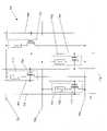
- FIG. 1illustrates a schematic circuit 100 of an array of memory cells, exemplified by a first and an identical second memory cell surrounded by the dotted lines 110 and 111 respectively.
- Each first memory cellincludes a resistively switching element 120 , 121 being coupled to a bitline 130 and to the drain of a selection transistor 140 and 141 respectively.
- the selection transistors 140 , 141are each coupled with its source to source potential, namely to a source line 150 , wherein the source potential can be ground potential, the source line 150 consequently a ground line. All selection transistors in this array of memory cells are coupled with their source to a single source line 150 being in this embodiment a plate. In this way a memory cell couples a transistor to a bit line via a resistively switching memory element.
- the selection transistors 140 , 141are double gate transistors as indicated, wherein each of the gates of a transistor is coupled to a different wordline, i.e. the first gate—on the left hand side of transistor 140 —is galvanically coupled to a first wordline 160 and the second gate—on the right hand side of transistor 140 —is galvanically coupled to a second wordline 161 . Consequently in order to fully open transistor 140 that is by applying an appropriate gate voltage to both gates the gate voltage must be applied to two wordlines, namely wordline 160 and 161 .
- the selection transistors 140 , 141are vertical transistors, wherein “vertical” describes that—with the wafer surface as a horizontal reference plane—a substantial part of the current flow is vertical or in other words the drain is arranged substantially above the body region where the conductive channel is formed which in turn is substantially arranged above the source of a transistor.
- the opposing gates of two adjacent transistors being coupled to the same bitline 130are coupled to the same wordline, i.e. the gate on the right hand side of transistor 140 and the gate on the left hand side of transistor 141 are coupled to wordline 161 . So if transistor 140 is opened by applying appropriate gate voltages to wordlines 160 and 161 , then at the same time the gate voltage is applied to one gate of transistor 141 .
- the transistorsare fully depleted, i.e. the depletion zones induced by the left and right hand gate electrodes in the active transistor area overlap.
- a positive voltage above the threshold voltagemust be applied to both gates to turn the transistor on. If only one gate electrode is raised high, that is a gate voltage above the threshold voltage of the double gate transistor is applied to only one of the gate electrodes, then the transistor is operated as a backgate controlled transistor, i.e. the effective threshold voltage is dependent on the voltage applied to the other (back) gate electrode, the threshold voltage decreasing with increased voltage applied to the backgate.
- the threshold voltage of the transistorcan be raised by applying a zero or even negative voltage to one of the gate electrodes and the transistor is not fully switched into the conducting state resulting in a considerably lower current flow.
- a voltage sufficiently below the threshold voltagewhich can be ground potential or a negative voltage, applied to both gate electrodes the transistor is turned off leading to a negligible current.
- the two corresponding wordlinesWhen writing a cell, that is when setting or resetting a cell by sending a comparatively high current pulse through the volume of resistively switching material, the two corresponding wordlines must be raised high to turn on its selection transistor. So for writing the first cell 110 , the wordlines 160 and 161 must be raised high to turn on selection transistor 140 and the voltage of the bitline 130 must be raised to an appropriate voltage so that a current pulse will flow through the resistively switching element 120 .
- the worst caseis that the selected cell is in high resistance state, whereas the adjacent memory cells connected to the same bitline are in a low resistance state.
- the selection transistorsare designed such that when reading a cell, the selection transistors of adjacent memory cells operate in the sub threshold regime so that the resistance of a transistor can be increased by at least 1-2 orders of magnitude so that the signal margin is large enough for being detected safely.
- Another embodiment of the described memory cell having two gate electrodes coupled to electrically independent wordlinesis that two different voltages can be applied to the two gates electrodes of one selection transistor.
- the two memory cells of FIG. 1are representative for a plurality of memory cells connected to one bitline thus forming a row of memory cells.
- a plurality of these rowscan be integrated in a single memory device including a plurality of bitlines and wordlines, wherein one memory cell can be selected by selecting the two corresponding wordlines and the corresponding bitline.
- FIG. 2is a schematic top-down view onto a cutout of a layout of an array of memory cells 200 including double gate selection transistors. Volumes of resistively switching material are not illustrated, as they are hidden by the bitlines. Also isolation material, into which for example the bitlines are embedded, is illustrated only where essential. Furthermore the source plate, onto which the structure is formed, is omitted, as well as further metallization levels above the bitline.
- a first and a second bit line 210 , 220 being the topmost elements in this top-down vieware exemplified.
- a plurality of identical bit linesis positioned adjacent and parallel to these. As will be explained in more detail in the following description, the bit lines are located above the surface plane of the original wafer.
- Reference signs 230 and 240denote a first and a second wordline, which exemplify a plurality of parallel wordlines.
- the wordlines 230 , 240are located below the bitlines 210 , 220 and at least partially below the surface plane of the original wafer, so that the wordlines are buried below the surface plane of the original wafer.
- each wordlineforms a plurality of gate electrodes of selection transistors.
- the active areas of the transistorsnamely the source, drain and body of a selection transistor, are located—indicated by arrow 260 —under the bitlines and between a pair of wordlines.
- STIshallow trench isolation
- reference numeral 260denotes arrows showing the periodicity of the bitlines 210 , 220 and wordlines 230 , 240 being 2F each, wherein F denotes the minimum feature size defined by conventional manufacturing methods. Consequently the cell size is 4F2.
- phase change cellWhile this concept is explicated with a phase change cell, it is not limited to phase change memory cells but can be applied to all resistive 1TnR memory concepts allowing the same cell architecture, i.e. cells having the bitline connected to the storage element directly and the transistor sources coupled to a common (ground) potential.
- an array layout as illustrated in FIG. 2can be achieved by two different structures, namely by a first embodiment including a buried wordline or a second structure including a conventional wordline. Both embodiments will be described in more detail below.
- FIG. 3 aillustrates a cross-section through two memory cells 300 , wherein the direction of the cut line is parallel to a bitline.
- the transistorcould also be formed as p-type transistor with adapted doping and voltages.
- a plate 320 of N+ doped semi-conducting materialis coupled to ground potential and serves as a ground line.
- the surface of this plate 320is used as a horizontal reference plane as it is comprised in each drawing.
- the drain 360 a, 360 b —N+ doped Si—of a selection transistoris positioned at the top of active area region 330 a, 330 b.
- the source region of the selection transistoris formed which is part of or directly coupled to the plate 320 .
- the transistor bodyis located between the n+-doped source 320 and the drain region 360 .
- the material of the bodiesis p-type doped.
- Each gate electrode 340 a, 340 bis electrically insulated by a gate oxide layer 350 a, 350 b against the active area 330 a.
- Gate electrode 340 afurthermore serves as one of two gate electrodes also for a transistor—not illustrated—adjacent on the left hand side of the drawing being the gate electrode on the right sidewall of a corresponding active area.
- gate electrode 340 bserves as one of two gate electrodes of a transistor including active area 330 b, whereby the gate electrode on the right hand side of active area 330 b is not illustrated in the drawing. Consequently each gate electrode serves as gate electrode for two adjacent transistors, the corresponding memory cells being coupled to one bit line 390 .
- the gate electrodes on one sidewall of the active areas of transistorsare galvanically coupled, in particular the coupled gate electrodes on one sidewall of active areas form a wordline. That is, in FIG. 3 a the gate electrode 340 a is coupled to the adjacent gate electrodes located in front of and also to the adjacent gate electrodes located behind the paper plane, so that these gate electrodes form a wordline running into the paper plane. Similarly gate electrode 340 b located on the opposite side of active area 330 a is coupled to adjacent gate electrodes—not illustrated—located in front of and behind the paper plane thus forming another wordline also running into the paper plane.
- a gate voltageis applied to two wordlines, namely those forming the gate electrodes at opposing sidewalls of the active area 330 a.
- the drain 360 a, 360 bis coupled to a bottom electrode contact 370 a, 370 b of a memory cell, the bottom electrode contact in turn placed on the drain and coupled to a volume of switching active material 380 a, 380 b.
- a volume of switching active material 380 a, 380 bin turn is placed on top of a bottom electrode 370 a, 370 b and coupled to a bitline 390 placed on top of the volumes of switching active material.
- both volumes 380 a, 380 b of switching active materialare coupled directly to one bitline 390 .
- These volumesexemplify a plurality of volumes of switching active material coupled directly to one bitline.
- FIG. 3 ba cross section through the structure with a cut line perpendicular to a bitline, i.e. in the direction of a wordline, is illustrated.
- the body region of an active area 330 a of a selection transistoris located on and galvanically coupled to the plate 320 which serves as a source plate electrode.
- the upper end of the body region of active area 330 a of the selection transistoris coupled to a drain 360 a, which in turn is galvanically coupled to a bottom electrode 370 a being in turn coupled to a volume of switching active material 380 a.
- a first gate electrode and thus a first wordlineis located in front of the paper plane of the drawing as indicated by the dotted line and reference numeral 340 a and a second gate electrode, in other words a second wordline, is located behind the paper plane, the two gates thus forming a double gate electrode for active area 330 a.
- a shallow trench insulation (STI) 350runs in an insulation trench parallel to bit lines 390 , thus insulating active areas of transistors of memory cells coupled to different bitlines.
- the insulation trenchdoes not extend into the source plate electrode 320 , so that body regions of adjacent transistors are electrically coupled in a lower region of the active areas. Consequently when operating the transistor charge carriers can dissipate from one active area into neighbouring active areas thus preventing an accumulation of charge carriers in one active area and thus preventing the impacts of a floating body transistor.
- the depth of the STIcan extend into the source plate electrode 320 thus forming isolated pillars of Si emerging from the source plate electrode 320 .
- the structure as illustrated in and described with reference to FIGS. 3 a, 3 bthus describes a vertical double gate transistor, wherein vertical describes the direction of the current flow from the source plate electrode 320 through the transistor body part of 330 a, 330 b and a drain 360 a, 360 b to a bottom electrode 370 a, 370 b coupled to a volume of switching active material 380 a, 380 b, which is coupled to a bitline 390 ( 390 a/ 390 b ).
- the gate electrodes 340 a, 340 bform a double gate electrode for each selection transistor at the sidewalls of an active area 330 a, 330 b, providing the advantages described above.
- the gate electrodes 340 a, 340 bare formed as stripes, they form wordlines running perpendicular to the bitlines 390 .
- each wordlinecan be coupled independently to a voltage, the two gates at the sidewalls of the active area of a selection transistor can be biased independently.
- FIG. 4illustrates a cross section through a structure when producing the selection transistors on a silicon wafer.
- the direction of the cut lineis parallel to a bitline and thus similar as in FIG. 3 a.
- the reference numeralsare the same as in FIG. 3 a where appropriate.
- the production of the structure illustratedstarts at the surface of a silicon wafer 310 , wherein the plane of the original top surface of the wafer is denoted by arrow 311 .
- the waferreceives an N+ implantation to produce a N+ doped layer which will serve as a source plate electrode 320 , wherein in the N+ must be implanted deeply into the wafer material, namely the Si of the wafer.
- Thiscan be either achieved by a high-energy implant, which transports the N+ deeply into the Si, or by an implant and an epitaxial growth of p-type doped Si on the surface so as to cover the N+ implanted layer by a Si deposit.
- the conductive layermay be part of the original substrate.
- a p-type epitaxial layeris deposited on top of an n+-type substrate wafer.
- the source plate electrodeserves to couple the source of a transistor to an appropriate source voltage, thus a corresponding source voltage is applied to the source plate electrode, e.g., ground potential.
- a pad oxide and pad nitrideas denoted by reference numeral 314 —and an optional hardmask layer can be deposited on the surface in a conventional manner for protection purposes and as patterning means.
- an insulation trench for a shallow trench isolationis etched.
- the insulation trenchis not illustrated as it runs parallel to the paper plane and in front of or behind the paper plane.
- the depth of STI trenchis at least half of the channel length of the transistor and may extend into the N+ doped source plate electrode.
- This trenchis filled with a conventional material suitable for a shallow trench insulation, for example an oxide as SiO.
- word line trenches for word linesare etched into the Si and isolation trenches using a conventional lithographic and etching method.
- the width of a trenchis denoted by reference numeral 312 .
- the word line trenchesare perpendicular to the insulation trenches these trenches cross the insulation trenches filled with an oxide, so that when etching the wafer material the STI material is to be etched also.
- the etching processmay be stopped before reaching the source plate electrode or the word line trench may extend into the source plate 320 .
- the word line trenchesform stripes of substrate material, which serve as active areas 330 a and 330 b of the transistors. These stripes are separated into transistor cells by the residual pieces of the insulation trenches. So the word lines separate the transistor cells in a first direction and the residual pieces of the insulation trenches separate the transistor cells in the direction of the word line trenches.
- the active areascan be further thinned in order to optimize the cooperation of the gate electrodes being positioned at opposite sidewalls of an active area. Another effect of thinning the active areas is that more space is produced for generating the gate oxide layer and the gate electrodes.
- a sacrificial oxidationcan be made optionally to generate a thin oxide layer protecting the active areas in subsequent processing steps and removing etch damage from the Si surface.
- the bottom of the trenchis vertically N+ implanted with an optional sacrificial sidewall spacer so as to galvanically couple the bottom of the trench to the source plate electrode 320 .
- the sacrificial oxide layeris removed and the inner sidewalls of wordline trenches are oxidized, that is a liner of electrically insulating oxide is provided, to form a liner of gate oxide in the wordline trench.
- the material of the gates 340 a, 340 b being the material of the wordlineis deposited and filled into the trenches.
- this materialpreferably is a metal, e.g., such as tungsten (W).
- Wtungsten
- the gate electrode materialwhich is the wordline material, is planarized with reference to the pad nitride using a conventional processing method, for example a conventional chemical/mechanical polishing (CMP) process.
- CMPchemical/mechanical polishing
- the gate electrode materialis recessed, so that the height of the wordline, which is also the height of the gate electrodes of a selection transistor, is defined as illustrated in the drawing, so that the top surface of the wordline lies under the original top surface of the wafer as denoted by arrow 311 .
- a device implantcan be performed for doping the drain of the transistor.
- the wordlines/gate electrodes 340 a and 340 bare covered by an electrically insulating oxide cap as indicated by reference numeral 313 .
- the pad nitride and oxide 314is removed in order to bare the top surface of the active area 330 a, 330 b.
- An optional N+ device implantcan be performed for doping the top of an active area 330 a, 330 b.
- another layer of Sican be deposited by selective epitaxial growth in order to widen the contact area of the active area 330 a, 330 b of a transistor.
- the bottom electrode contact for contacting a volume of phase change materialcan be formed in a conventional manner above the active area 330 a, 330 b. Also the volumes of phase change material and the bitlines can be formed using conventional method steps.
- the wordline being formed by the gate electrodes 340 a and 340 bis formed below the top surface of the original wafer and is thus buried. Moreover, the source plate electrode 320 , the active areas 330 a, 330 b and the gate electrodes forming the wordlines are placed below the surface 311 of the original wafer.
- a second structureproposing a double gate memory cell having a conventional wordline stack structure as described in the following.
- FIGS. 5 a and 5 billustrate a structure having similarities with that of FIGS. 3 a and 3 b with the exception of the conventional wordline stack structure.
- FIG. 5 aillustratesa cross section through a memory cell wherein the cut line is parallel to a bitline.
- a layer of N+ doped silicon on a wafer of Si 510serves as a source plate electrode 520 , onto which a vertical transistor including a p-type doped body region 530 a or 530 b and an N type doped drain 560 a, 560 b is formed.
- a gate oxide liner 550 a, 550 binsulates a gate electrode 540 a, 540 b from the active areas 530 a, 530 b and the source plate electrode 520 and the drain area 560 a,b.
- the gate electrodes 540 a and 540 bform a double gate electrode for the transistor having the active area 530 a.
- the material of the gate electrodes 540 a, 540 bis poly silicon (poly Si). This has the advantage that poly Si is less complex to process when forming the gate electrodes, in particular when filling a trench.
- a gate conductor 570 a, 570 b of a good conducting materialis formed on top of the poly Si gate electrodes 540 a and 540 b.
- This layer 570 a, 570 bis located above the top surface—denoted by 511 —of the original wafer, so that in this embodiment the wordline is not buried under the top surface of the wafer.
- the gate electrodesare running into the paper plane the gate conductor 570 a, 570 b also runs into the paper plane.
- the gate conductors 570 a, 570 bare embedded in an electrically insulating material 580 a, 580 b to electrically insulate them from surrounding elements, for example from bottom electrode contacts 590 a, 590 b.
- the bottom electrode contacts 590 a, 590 beach contact a volume of phase change material 5100 a, 5100 b at the lower side, which in turn are coupled directly to a bitline 5110 .
- FIG. 5 billustrates the structure of a memory cell and an associated selection transistor in a cross sectional view through the memory cell and perpendicular to a bitline and thus perpendicular to the view as in FIG. 5 a.
- N+ doped silicon 520serving as a source plate electrode.
- a pillar of weakly p-type doped Sibeing the body of active area 530 a of the selection transistor extends from the source plate electrode 520 .
- a N+ doped drain 560 ais placed on the body of the transistor and couples to the bottom electrode 590 a of a memory cell, which includes a volume of phase change or switching active material 5100 a being in turn coupled to a bitline 5110 .
- the dashed line of the gate electrodes 540 a, 540 bshall indicate, that in this view one gate electrode is located in front of and the other is located behind the paper plane.
- An insulation trench for a shallow trench isolation (STI) 5120electrically separates the active area 530 a from surrounding elements, in particular from the drains of adjacent selection transistors.
- STIshallow trench isolation
- the shallow trench isolation 5120extends into or reaches the source plate electrode 520 and thus separates the active area 530 a of the illustrated selection transistor from the active area of an adjacent transistor.
- the depth of the trench of this STIshall reach down to at least below the drain area of the transistor but may stop before the source plate electrode 520 , so that the STI does not separate between the active areas of adjacent transistors.
- FIG. 6illustratesa cross sectional view with the cut line being parallel to a bitline and through a transistor, the transistor having a double gate electrode and a conventional wordline, at a processing stage just before the gate conductor is etched.
- the production of the structurestarts from an undoped or weakly p-type doped wafer 610 wherein the plane of the original top surface of the wafer is denoted by arrow 611 .
- the wafer in this embodimentreceives an N+ doped source layer.
- a pad oxidedenoted by reference numeral 614 —and a pad nitride and an optional hardmask layer—none of the layers illustrated—can be deposited on the surface in a conventional manner for protection purposes and as patterning means.
- trenches for a shallow trench isolation (STI) between the active areas of adjacent transistorsare etched using conventional lithographic and etching methods. These trenches are not illustrated in the drawing as they run parallel to the bitlines and are located in front of and behind the paper plane of this drawing. As mentioned above with regard to FIG. 5 b the depth of the trench for the STI at least must be below the drain of the transistor and may end before reaching the source plate electrode 620 or may extend into it.
- the trenches for the STIare filled with a suitable insulation material, which typically may be an oxide such as SiO using a conventional method.
- wordline trenches running perpendicular to the insulation trenches and perpendicular to bitlinesare formed using conventional lithographic and etching processing steps. As these trenches run perpendicular to the insulation trenches the Si of the wafer and the oxide of the STI must be etched. In the drawing the wordline trenches run into the paper plane and the width is indicated by reference numeral 612 . The depth of the wordline trenches may either extend into or may stop above the source plate electrode 620 .
- the Sican be optionally thinned by isotropic etching and the pad nitride and optionally the pad oxide may be removed. Then a sacrificial oxide layer can be produced optionally serving as a protection in subsequent processing steps, and which will be removed before the gate oxide for the transistor is produced or deposited.
- the bottom of the wordline trenchesis N+ implanted to galvanically connect the bottom of a wordline trench to the source plate electrode 620 , whereby a sacrificial sidewall spacer—not illustrated—can be formed optionally in the wordline trench to ensure that the bottom only is implanted.
- electrically insulating materialtypically an oxide such as SiO will be formed at the Si sidewalls of the active area to form a liner of insulating material which will serve as a gate oxide layer 650 a, 650 b.
- the remaining of the wordline trenchesis filled with poly Si to form the gate electrodes 640 a and 640 b.
- the gate electrodes 640 a and 640 bform the double gate for the active area 630 a.
- the deposited gate electrode materialoptionally may be planarized to the pad nitride layer by using a conventional planarization process such as chemical-mechanical polishing (CMP).
- the pad nitrideis removed leaving the thick pad oxide 614 on the top surface of the chip.
- the layers for the gate conductorare deposited. That is an optional layer of poly Si 660 , a layer of a metal 670 to form the wordline from and a layer of insulating silicon nitride (SiN) 680 are deposited in this order onto the surface of the chip using conventional deposition methods.
- This stack of layersis processed by using conventional lithographic and etching process to form a gate conductor. That is the three layers are shaped into lines positioned on top of the gate electrodes thus providing a conventional wordline made of a metal located on and electrically coupled to the gate electrodes 640 a and 640 b.
- suitable liners and sidewall spacersare formed from oxide and/or SiN to electrically insulate the sidewalls of the lines against the active areas 630 a, 630 b and bottom electrodes, which will be formed on top of the active areas.
- active areas 630 a and 630 bare coupled to a volume of for example phase change material, which in turn will be connected to a bitline.
- device implantsto N+ dope the active areas and a selective epitaxial growth of Si to widen the contact area of the active areas.
- a salicidation processmay be used to improve the contact resistance.
- Areas or volumes between the different functional elements formed so farare filled with an interleveldielectric, which typically is an insulating oxide such as SiO. This layer is then planarized to gate.
- etchingis selective to the SiN covering the gate electrode and the gate conductor respectively, in order to bare the top surface of the active areas.
- a device junction implantcan be performed in order to improve the conductivity between active areas and bottom electrodes to be formed.
- bottom electrodesare formed on top of the active areas using conventional process. Volumes of phase change material or other suitable switching active material will be formed and coupled to the bottom electrodes with their one end. On top of the volumes of switching active material bitlines will be formed.
- FIG. 7illustrates a schematic circuit 700 of an embodiment of the invention described above, wherein an array of memory cells is exemplified by four memory cells 710 , 711 , 712 , 713 , 714 .
- the memory cellsare identical to cell 710 including a volume of resistively switching material 720 and a double gate selection transistor 740 .
- all selection transistorsare coupled to a common source line being formed as a source plate electrode and which can be coupled to ground potential.
- the drain of each selection transistoris coupled to the volume of switching active material being in turn coupled to a bit line, such that in this way each memory cell couples a transistor to a bit line via a resistively switching memory element.
- the selection transistorsare double gate transistors. Each of the gate electrodes of a transistor is coupled to a different word line. Hence in order to open a selection transistor a gate voltage must be applied to two—adjacent—word lines.
- the memory cellsare arranged such that the drains of selection transistors of adjacent memory cells in the direction of the word lines 760 - 764 , whose gate electrodes are consequently are coupled to the same word lines, are coupled to different bit lines, wherein the next cell is coupled to the next bit line but one.
- adjacent memory cellswhich are coupled to the same bit line, are coupled to different word lines.
- cells 710 and 712are both coupled to bit line 730 and are adjacent to each other in bit line direction.
- the gate electrodes of the selection transistor of cell 710are coupled to word lines 760 and 761 respectively and the gate electrodes of the selection transistor of cell 712 are coupled to word lines 762 and 763 respectively.
- memory cells coupled to the same bitlineare coupled to different word lines and—in other words—cells coupled to the same word lines are coupled to different bit lines.
- a memory cellcan be selected by selecting one bit line and a pair of word lines, but in contrast to the embodiment described above when selecting a memory cell by applying a voltage to the bit line and the corresponding word lines, the gate voltages of the adjacent memory cell in bit line direction remain unaffected. Consequently there is no need to form the transistors as fully depleted transistors.
- the memory cells and thus the corresponding transistor cellsare located at crossing points of the pairs of word lines, wherein the cells are arranged like on a checkerboard. That is in word line direction the cells are located at every second crossing point of a pair of word lines and a bit line and furthermore are arranged staggered to the adjacent row of cells by one crossing point, so that also in bit line direction the cells are located at every second crossing point.
- FIG. 8illustrates a top down view on the variation of the embodiment described above, which is an array of memory cells 800 including double gate transistors and volumes of resistively switching material.
- first and a second bit line 810 , 820are the topmost elements in this view, which exemplify a plurality of parallel bit lines and which are located above the surface plane of the original wafer.
- a first and a second word line 830 , 840exemplify a plurality of parallel word lines being positioned below the bit lines and at least partially below the surface plane of the original wafer, thus being buried below the surface plane.
- Each word lineforms a plurality of gate electrodes being insulated by a layer of gate dielectric 850 , which can be an oxide such as SiO.
- STIshallow trench isolation
- Reference numeral 860denotes the location—encircled in the drawing—of the active areas of the transistors, which are positioned below the bit lines and between the word lines.
- the active areasare arranged staggered.
- every second transistoris omitted, either in bit line direction or in word line direction.
- each transistor and consequently each memory cell including the transistorcan be selected by applying an appropriate voltage to one bit line and two word lines, wherein the voltage applied to the word lines leaves the adjacent transistor in bit line direction unaffected, i.e. the gate voltage applied to the word lines does not have impact on a gate electrode of the adjacent transistor.
- the conductivity of the adjacent transistoris unaffected by selecting the transistor and accordingly the transistors may not be fully depleted transistors.
- Reference numerals 880denote arrows indicating the periodicity of the bit lines and the word lines, each being 2F, although the drawing is not drawn to scale. Accordingly the cell size of a memory cell is approximately 8F2.
- FIG. 9 aillustrates a cross section through a memory cell including a transistor, wherein the direction of the cut line is in bit line direction.
- a source plate 920 of N+ doped semi-conducting material in a wafer 910there is a source plate 920 of N+ doped semi-conducting material in a wafer 910 , the source plate for example being coupled to ground potential and serving as a ground plate electrode.
- a transistor body 930 of slightly doped p-type siliconis coupled with its lower end to the source plate electrode 920 and with its opposing end forming the drain 960 to a bottom electrode 970 , which in turn is coupled to a volume of resistively switching material 980 .
- the volume of resistively switching materialin turn is coupled to a bit line 990 .
- Word lines 940 a, 940 bare arranged on opposing sidewalls of transistor body 930 thus forming the gate electrodes of the transistor and are galvanically insulated by gate dielectric 950 a, 950 b from the transistor body.
- the gate electrodesabut against insulating material of the shallow trench insulation 9100 .
- adjacent cells in bit line directiondo not have a common or shared gate electrode.
- the adjacent transistor in bit line directionincludes a pair of gate electrodes formed by a parallel pair of word lines, which are not illustrated in this view.
- FIG. 9 billustrates a cross sectional view through the structure in word line direction, that is perpendicular to the cut line as in FIG. 9 a.
- a transistor body 930formed from slightly p-doped semiconductor material, of a selection transistor is located on and coupled to a N+ doped source plate electrode 920 being formed in the substrate 910 of a wafer, the lower end of the body 930 thus forming the source of the transistor.
- the upper end of the transistor body 930 referenced by numeral 960is N+ doped and forms the drain of the transistor, which is coupled to a bottom electrode 970 being in turn coupled to a volume of resistively switching material 980 .
- the volume of resistively switching materialis coupled to bit line 990 .
- the insulating material of a shallow insulation trench 9100is located at two opposing sidewalls of transistor body 930 thus separating this transistor body from that of an transistor body adjacent in word line direction.
- the word lines forming the gate electrodesare located in front of and behind the paper plane.
- the dotted line 940shall indicate the location of the gate electrodes in front of and behind the paper plane.
- the dimension of the transistor body 930is in the direction of the cut line significantly larger than in bit line direction and also larger than that as illustrated in the first embodiment.
- a transistor body having a bigger cross-sectional area in the direction of the current flow, which in this view is vertically,can be achieved.
- Thisis advantageous in particular for resistively switching memory cells, because for changing the resistance in the volume of the resistively switching memory cell a strong current may be necessary.
- the dimension of the transistor body in word line directionmay be up to 3F.
- the described embodiment of an array of vertical transistorscan be achieved by either of the two methods described for the first embodiment, but wherein the masks for producing the transistors and for producing the memory elements are amended such that every second cell is omitted in order to achieve a staggered arrangement of memory cells like on a checkerboard.
Landscapes
- Semiconductor Memories (AREA)
Abstract
Description
- The invention relates to a transistor, a memory cell array and a method for forming and operating a memory device with at least one memory cell, in particular a resistively switching, e.g., a phase change memory cell, and to a memory device.
- Conventional memory devices, in particular semiconductor memory devices, can be differentiated into a first group of functional memory devices, e.g., PLAs, PALs, etc., a second group of table memory devices, e.g., ROM devices such as PROMs, EPROMs, EEPROMs, flash memories, etc. Furthermore there is a third group of RAM devices, such as DRAMs and SRAMs.
- Recently “resistive” or “resistively switching” memory devices have also become known, e.g., so called Phase Change Memories (“PCMs”) or Conducting Bridge (CB) memories or magnetoresistive memories (MRAM) or resistive RAM (RRAM).
- In a “resistive” or “resistively switching” memory cell, an “active” or “switching active” material, which usually is positioned between two suitable electrodes, i.e. an anode and a cathode, can be switched between a conductive and a less conductive state by an appropriate switching process. The conductive state can be assigned a logic one and the less conductive state can be assigned a logic zero, or vice versa, which may, for instance, correspond to the logic arrangement of a bit.
- For phase change memories (PCRAMs), for instance, an appropriate chalcogenide compound, for example Ge—Sb—Te (GST) or an In—Sb—Te compound, may be used as a “switching active” material that is positioned between two corresponding electrodes. This “switching active”, e.g., the chalcogenide material, can be switched between an amorphous and a crystalline state, wherein the amorphous state is the relatively weakly conducting state, which accordingly can be assigned a logic zero, and the crystalline state, i.e. a relatively strongly conductive state, accordingly can be assigned a logic one. In the following this material will be referred to as the switching active material.
- To achieve a change from the amorphous, i.e. a relatively weakly conductive state of the switching active material, to a crystalline, i.e. a relatively strongly conductive state, the material has to be heated. For this purpose a heating current pulse is sent through material, which heats the switching active material beyond its crystallization temperature thus lowering its resistance. In this way the value of a memory cell can be set to a first logic state.
- Vice versa, the switching material can be heated by applying a relatively high current to the cell which causes the switching active material to melt and by “quench cooling” the material can brought into an amorphous, i.e. relatively weakly conductive state, which may be assigned a second logic state, that is to reset the first logic state.
- Various concepts have been proposed for PCRAM cells, for example from S. J. Ahn, “Highly Manufacturable High Density Phase Change Memory of 64 MB and Beyond”, IEDM 2004, and H. Horii et al. “A novel cell technology using N-doped GeSbTe films for phase change RAM”, VLSI, 2003, and Y. N. Hwang et al “Full integration and reliability evaluation of phase-change RAM based on 0.24 um-CMOS technologies”, VLSI, 2003, and S. Lai et al “OUM—a 180 nm non-volatile memory cell element technology for stand alone and embedded applications”, IEDM 2001, or the edge contact cell by Y. H. Ha et al “An edge contact cell type cell for phase change RAM featuring very low power consumption”, VLSI, 2003.
- To be cost competitive a small cell size is required allowing a high density of memory cells in a memory cell array.
- A disadvantage of the proposed memory cells is the use of planar array transistors or transistors having the source/drain contacts in the same horizontal plane, for example FinFETs. Such a design prohibits shrinking the cell size below 6F2 for geometrical reasons, because the size of a cell includes the area needed for the transistor to select the cell.
- US2005/0001257A1 discloses a DRAM memory cell having vertical transistor cells formed in a substrate including lower source/drain regions connected to a common connection plate. Upper source/drain regions of the transistor cells impart a contact connection to a storage capacitor. The array of transistor cells is formed by wordline trenches, wherein the wordlines in the trenches form gate electrodes of the transistors, and by isolation trenches (STI) running perpendicular to the wordline trenches. A disadvantage of the proposed structure is the need to accommodate and form two electrically isolated spacer wordlines in one wordline trench.
- Consequently it is desirable to provide a novel design of a selection transistor for a memory device with a plurality of memory cells, in particular phase change memory cells, and a corresponding method for forming the transistors avoiding the abovementioned problems.
- For these and other reasons, there is a need for the present invention.
- In one embodiment, the invention provides an array of vertical transistors in a substrate for selecting one of a plurality of memory cells, each memory cell coupling a transistor cell to a bit line via a memory element and being addressable by selecting two word lines and the bit line, the array of vertical transistors defined by a plurality of word line trenches and a plurality of crossing, perpendicular insulation trenches in the substrate, the word line trenches separating transistor cells in the direction of insulation trenches and the insulation trenches separating transistor cells in the direction of word line trenches, wherein one word line trench takes one word line, and wherein a first word line in a first word line trench forms a plurality of gate electrodes on one sidewall of active areas of a first and a second, adjacent row of transistor cells in word line direction, and wherein a second word line in an adjacent word line trench forms a plurality of gate electrodes on the opposite sidewall of active areas of the second and of a third row of transistor cells in wordline direction.
- Another embodiment of the invention is directed at an array of vertical transistors in a substrate for selecting one of a plurality of memory cells, each memory cell coupling a transistor cell to a bit line via a memory element and being addressable by selecting two word lines and the bit line, the array of vertical transistors defined by a plurality of word line trenches and a plurality of crossing, perpendicular insulation trenches in the substrate, the word line trenches separating transistor cells in the direction of insulation trenches and the insulation trenches separating transistor cells in the direction of word line trenches, wherein one word line trench takes one line of gate electrodes of one line of adjacent transistor cells in wordline direction, the gate electrodes being electrically coupled to a gate conductor positioned above the wordline trench, wherein a first line of gate electrodes in a first word line trench forms a plurality of gate electrodes on one sidewall of active areas of a first and a second, adjacent row of transistor cells in word line direction, and wherein a second line of gate electrodes in an adjacent word line trench forms a plurality of gate electrodes on the opposite sidewall of active areas of the second and of a third row of transistor cells in wordline direction.
- The invention proposes a method for producing an array of vertical transistor cells in a substrate including the following method processes: providing a conductive layer within the substrate, the conductive layer covered by a less conductive and at least partially oppositely doped substrate layer;
- forming a plurality of parallel insulation trenches extending along a first direction and filling the insulation trenches with an insulating material;
- forming a plurality of parallel wordline trenches extending along a second direction perpendicular to the first direction thus forming pillars of substrate material emerging from the substrate and serving as active areas of the transistor cells; producing a layer of gate dielectric in a first wordline trench and filling with a conductive material thus forming gate electrodes at a sidewall of a first and of a second, adjacent line of active areas in wordline direction thus forming a wordline; producing a layer of gate dielectric in at least a second, adjacent wordline trench and filling with a conductive material thus forming gate electrodes at an opposite sidewall of the first line of active areas and at a sidewall of a third, adjacent line of active areas in wordline direction thus forming a second, adjacent wordline.
- In another embodiment the invention proposes a method for producing an array of vertical transistor cells in a substrate including the following methodprocesses: providing a conductive layer within the substrate, the conductive layer covered by a less conductive substrate layer;
- forming a plurality of parallel insulation trenches extending along a first direction and filling the insulation trenches with an insulating material; forming a plurality of parallel wordline trenches extending along a second direction perpendicular to the first direction thus forming pillars of substrate material emerging from the conductive layer within the substrate and serving as active areas of the transistor cells;
- producing a layer of gate dielectric in a first wordline trench and filling with a conductive material thus forming gate electrodes at a sidewall of a first and of a second, adjacent line of active areas in wordline direction thus forming a wordline;
- producing a layer of gate dielectric in at least a second, adjacent wordline trench and filling with a conductive material thus forming gate electrodes at an opposite sidewall of the first line of active areas and at a sidewall of a third, adjacent line of active areas in wordline direction thus forming a second, adjacent word line.
- A method of driving a double gate transistor is described, the transistor including an active area, a first gate electrode located on a first sidewall of the active area and a second gate electrode located at an opposite sidewall of the active area, the first gate electrode coupled to a first word line and the second gate electrode coupled to a second word line, wherein the transistor has first state being defined by a first voltage potential applied to both word lines opening the transistor, a second state defined by the first voltage potential being applied to the first word line and a second voltage potential being applied to the second word line to lower the conductivity of the transistor by at least one order of magnitude.
- Also a method of driving a first and a second, adjacent double gate transistor in an array of double gate transistors is proposed, the first double gate transistor including a first gate electrode coupled to a first word line and a second gate electrode coupled to a second word line, the second double gate transistor including a first gate electrode coupled third word line and a second gate electrode coupled to the second word line, the first and second transistors thus sharing the gate electrode coupled to the second word line, wherein when opening the first transistor a positive gate voltage is applied to the first and second word line and a ground or negative voltage is applied to the third word line thus closing the second transistor.
- In another embodiment an array of transistors in a substrate for selecting one of a plurality of memory cells is described, each memory cell coupling a transistor to a bit line via a memory element and being addressable by selecting a pair of word lines and one perpendicular bit line, the array of transistors formed by a plurality of word line trenches forming stripes of substrate material serving as active areas of the transistors, the stripes separated by pieces of insulation trenches, thus the word lines trenches separating transistor cells in a first direction and the pieces of insulation trenches separating transistor cells in the direction of word line trenches, wherein one word line trench takes one word line, and wherein a first word line of a pair forming a plurality of gate electrodes on one sidewall of active areas of a row of transistor cells in word line direction, the other word line of the pair forming a plurality of gate electrodes on the opposite sidewall of the active areas of the row of transistor cells in word line direction, and wherein the transistors are located at every second crossing point of a pair of word lines and a bit line, whereby transistors in an adjacent row are arranged staggered by one bit line, the transistors thus arranged like on a checkerboard.
- Further features and advantages of the present invention will become apparent from the following detailed description of the invention made with reference to the accompanying drawings.
- The accompanying drawings are included to provide a further understanding of the present invention and are incorporated in and constitute a part of this specification. The drawings illustrate the embodiments of the present invention and together with the description serve to explain the principles of the invention. Other embodiments of the present invention and many of the intended advantages of the present invention will be readily appreciated as they become better understood by reference to the following detailed description. The elements of the drawings are not necessarily to scale relative to each other. Like reference numerals designate corresponding similar parts.
FIG. 1 illustrates a schematic circuit diagram of an array of memory cells.FIG. 2 illustrates a schematic top-down view of an array layout of double gate cells.FIGS. 3 aand3billustrate schematic cross sectional views of a memory cell.FIG. 4 illustrates a schematic cross sectional view of a memory cell at a processing stage.FIGS. 5 aand5billustrate schematic cross sectional views of a variation of a memory cell.FIG. 6 illustrates a schematic cross sectional view of a variation of a memory cell at a processing stage.FIG. 7 illustrates a schematic circuit diagram of an alternative embodiment of the invention.FIG. 8 illustrates a top down view on the alternative array layout of double gate cellsFIGS. 9 aand9billustrate schematic cross sectional views of the alternative- In the following Detailed Description, reference is made to the accompanying drawings, which form a part hereof, and in which is shown by way of illustration specific embodiments in which the invention may be practiced. In this regard, directional terminology, such as “top,” “bottom,” “front,” “back,” “leading,” “trailing,” etc., is used with reference to the orientation of the Figure(s) being described. Because components of embodiments of the present invention can be positioned in a number of different orientations, the directional terminology is used for purposes of illustration and is in no way limiting. It is to be understood that other embodiments may be utilized and structural or logical changes may be made without departing from the scope of the present invention. The following detailed description, therefore, is not to be taken in a limiting sense, and the scope of the present invention is defined by the appended claims.
FIG. 1 illustrates aschematic circuit 100 of an array of memory cells, exemplified by a first and an identical second memory cell surrounded by thedotted lines - Each first memory cell includes a
resistively switching element bitline 130 and to the drain of aselection transistor selection transistors source line 150, wherein the source potential can be ground potential, thesource line 150 consequently a ground line. All selection transistors in this array of memory cells are coupled with their source to asingle source line 150 being in this embodiment a plate. In this way a memory cell couples a transistor to a bit line via a resistively switching memory element. - The
selection transistors transistor 140—is galvanically coupled to afirst wordline 160 and the second gate—on the right hand side oftransistor 140—is galvanically coupled to asecond wordline 161. Consequently in order to fullyopen transistor 140 that is by applying an appropriate gate voltage to both gates the gate voltage must be applied to two wordlines, namely wordline160 and161. - The
selection transistors - The opposing gates of two adjacent transistors being coupled to the
same bitline 130 are coupled to the same wordline, i.e. the gate on the right hand side oftransistor 140 and the gate on the left hand side oftransistor 141 are coupled towordline 161. So iftransistor 140 is opened by applying appropriate gate voltages to wordlines160 and161, then at the same time the gate voltage is applied to one gate oftransistor 141. - In one embodiment, the transistors are fully depleted, i.e. the depletion zones induced by the left and right hand gate electrodes in the active transistor area overlap. For fully depleted n-type double gate transistors a positive voltage above the threshold voltage must be applied to both gates to turn the transistor on. If only one gate electrode is raised high, that is a gate voltage above the threshold voltage of the double gate transistor is applied to only one of the gate electrodes, then the transistor is operated as a backgate controlled transistor, i.e. the effective threshold voltage is dependent on the voltage applied to the other (back) gate electrode, the threshold voltage decreasing with increased voltage applied to the backgate. In this way, the threshold voltage of the transistor can be raised by applying a zero or even negative voltage to one of the gate electrodes and the transistor is not fully switched into the conducting state resulting in a considerably lower current flow. In case there is a voltage sufficiently below the threshold voltage, which can be ground potential or a negative voltage, applied to both gate electrodes the transistor is turned off leading to a negligible current.
- When writing a cell, that is when setting or resetting a cell by sending a comparatively high current pulse through the volume of resistively switching material, the two corresponding wordlines must be raised high to turn on its selection transistor. So for writing the
first cell 110, thewordlines selection transistor 140 and the voltage of thebitline 130 must be raised to an appropriate voltage so that a current pulse will flow through theresistively switching element 120. - Due to the voltage applied to the
wordlines 160 and161 a voltage is also applied to one gate of the selection transistors of adjacent memory cells. However, as the opposite gate electrode of the adjacent memory cells is held low, that is at ground or an even lower potential, the current flow through the selection transistors of the adjacent memory cells is below the writing threshold the current flowing through these cells thus leaving them unmodified. - When reading a memory cell, the worst case is that the selected cell is in high resistance state, whereas the adjacent memory cells connected to the same bitline are in a low resistance state. So in order to minimize the current flowing through the adjacent memory cells, the selection transistors are designed such that when reading a cell, the selection transistors of adjacent memory cells operate in the sub threshold regime so that the resistance of a transistor can be increased by at least 1-2 orders of magnitude so that the signal margin is large enough for being detected safely.
- Another embodiment of the described memory cell having two gate electrodes coupled to electrically independent wordlines is that two different voltages can be applied to the two gates electrodes of one selection transistor.
- The two memory cells of
FIG. 1 are representative for a plurality of memory cells connected to one bitline thus forming a row of memory cells. A plurality of these rows can be integrated in a single memory device including a plurality of bitlines and wordlines, wherein one memory cell can be selected by selecting the two corresponding wordlines and the corresponding bitline. FIG. 2 is a schematic top-down view onto a cutout of a layout of an array ofmemory cells 200 including double gate selection transistors. Volumes of resistively switching material are not illustrated, as they are hidden by the bitlines. Also isolation material, into which for example the bitlines are embedded, is illustrated only where essential. Furthermore the source plate, onto which the structure is formed, is omitted, as well as further metallization levels above the bitline.- A first and a
second bit line - Reference signs230 and240 denote a first and a second wordline, which exemplify a plurality of parallel wordlines. The
wordlines bitlines - The sidewalls of the wordlines are covered by a layer of insulating
oxide 250, which forms the gate oxide of selection transistors. Thus each wordline forms a plurality of gate electrodes of selection transistors. The active areas of the transistors, namely the source, drain and body of a selection transistor, are located—indicated byarrow 260—under the bitlines and between a pair of wordlines. - The areas between the bitlines and also between the wordlines—referenced by
arrow 270—are filled with an insulating material forming a shallow trench isolation (STI). - Even though the drawing is not drawn to scale
reference numeral 260 denotes arrows showing the periodicity of thebitlines wordlines - While this concept is explicated with a phase change cell, it is not limited to phase change memory cells but can be applied to all resistive 1TnR memory concepts allowing the same cell architecture, i.e. cells having the bitline connected to the storage element directly and the transistor sources coupled to a common (ground) potential.
- It is to be noted that an array layout as illustrated in
FIG. 2 can be achieved by two different structures, namely by a first embodiment including a buried wordline or a second structure including a conventional wordline. Both embodiments will be described in more detail below. FIG. 3 aillustrates a cross-section through twomemory cells 300, wherein the direction of the cut line is parallel to a bitline.- The following description is for an n-type transistor. Even if not described here, the transistor could also be formed as p-type transistor with adapted doping and voltages.
- In a wafer310 a
plate 320 of N+ doped semi-conducting material is coupled to ground potential and serves as a ground line. In the following description also throughout the description the surface of thisplate 320 is used as a horizontal reference plane as it is comprised in each drawing. - In the drawing two
active area regions drain 360a,360b—N+ doped Si—of a selection transistor is positioned at the top ofactive area region plate 320. Between the n+-dopedsource 320 and the drain region360, the transistor body is located. The material of the bodies is p-type doped. - There are two
gate electrodes active areas 330a,so that this transistor is a double gate transistor. Eachgate electrode gate oxide layer active area 330a. Gate electrode 340afurthermore serves as one of two gate electrodes also for a transistor—not illustrated—adjacent on the left hand side of the drawing being the gate electrode on the right sidewall of a corresponding active area. Alsogate electrode 340bserves as one of two gate electrodes of a transistor includingactive area 330b,whereby the gate electrode on the right hand side ofactive area 330bis not illustrated in the drawing. Consequently each gate electrode serves as gate electrode for two adjacent transistors, the corresponding memory cells being coupled to onebit line 390.- As mentioned above the gate electrodes on one sidewall of the active areas of transistors are galvanically coupled, in particular the coupled gate electrodes on one sidewall of active areas form a wordline. That is, in
FIG. 3 athegate electrode 340ais coupled to the adjacent gate electrodes located in front of and also to the adjacent gate electrodes located behind the paper plane, so that these gate electrodes form a wordline running into the paper plane. Similarlygate electrode 340blocated on the opposite side ofactive area 330ais coupled to adjacent gate electrodes—not illustrated—located in front of and behind the paper plane thus forming another wordline also running into the paper plane. - Consequently for driving the transistor cell including the
active area 330aa gate voltage is applied to two wordlines, namely those forming the gate electrodes at opposing sidewalls of theactive area 330a. - The
drain 360a,360bis coupled to abottom electrode contact active material active material bottom electrode bitline 390 placed on top of the volumes of switching active material. - According to the direction of the cut line in the drawing both
volumes bitline 390. These volumes exemplify a plurality of volumes of switching active material coupled directly to one bitline. - Turning now to
FIG. 3 ba cross section through the structure with a cut line perpendicular to a bitline, i.e. in the direction of a wordline, is illustrated. - As described above the body region of an
active area 330aof a selection transistor is located on and galvanically coupled to theplate 320 which serves as a source plate electrode. The upper end of the body region ofactive area 330aof the selection transistor is coupled to adrain 360a,which in turn is galvanically coupled to abottom electrode 370abeing in turn coupled to a volume of switchingactive material 380a. - In this embodiment, a first gate electrode and thus a first wordline is located in front of the paper plane of the drawing as indicated by the dotted line and reference numeral340aand a second gate electrode, in other words a second wordline, is located behind the paper plane, the two gates thus forming a double gate electrode for
active area 330a. - A shallow trench insulation (STI)350 runs in an insulation trench parallel to bit
lines 390, thus insulating active areas of transistors of memory cells coupled to different bitlines. - In this embodiment, the insulation trench does not extend into the
source plate electrode 320, so that body regions of adjacent transistors are electrically coupled in a lower region of the active areas. Consequently when operating the transistor charge carriers can dissipate from one active area into neighbouring active areas thus preventing an accumulation of charge carriers in one active area and thus preventing the impacts of a floating body transistor. - However, in a variation the depth of the STI can extend into the
source plate electrode 320 thus forming isolated pillars of Si emerging from thesource plate electrode 320. - The structure as illustrated in and described with reference to
FIGS. 3 a,3bthus describes a vertical double gate transistor, wherein vertical describes the direction of the current flow from thesource plate electrode 320 through the transistor body part of330a,330band adrain 360a,360bto abottom electrode active material - The
gate electrodes active area gate electrodes bitlines 390. As each wordline can be coupled independently to a voltage, the two gates at the sidewalls of the active area of a selection transistor can be biased independently. FIG. 4 illustrates a cross section through a structure when producing the selection transistors on a silicon wafer. The direction of the cut line is parallel to a bitline and thus similar as inFIG. 3 a.The reference numerals are the same as inFIG. 3 awhere appropriate.- The production of the structure illustrated starts at the surface of a
silicon wafer 310, wherein the plane of the original top surface of the wafer is denoted byarrow 311. - Starting with a weakly doped substrate, the wafer receives an N+ implantation to produce a N+ doped layer which will serve as a
source plate electrode 320, wherein in the N+ must be implanted deeply into the wafer material, namely the Si of the wafer. This can be either achieved by a high-energy implant, which transports the N+ deeply into the Si, or by an implant and an epitaxial growth of p-type doped Si on the surface so as to cover the N+ implanted layer by a Si deposit. - The conductive layer may be part of the original substrate. For this, a p-type epitaxial layer is deposited on top of an n+-type substrate wafer.
- The source plate electrode serves to couple the source of a transistor to an appropriate source voltage, thus a corresponding source voltage is applied to the source plate electrode, e.g., ground potential.
- On the surface of the wafer a pad oxide and pad nitride—as denoted by
reference numeral 314—and an optional hardmask layer can be deposited on the surface in a conventional manner for protection purposes and as patterning means. - In a next process an insulation trench for a shallow trench isolation (STI) is etched. In this drawing the insulation trench is not illustrated as it runs parallel to the paper plane and in front of or behind the paper plane. As can be seen in
FIG. 3 band denoted byreference sign 350athe depth of STI trench is at least half of the channel length of the transistor and may extend into the N+ doped source plate electrode. This trench is filled with a conventional material suitable for a shallow trench insulation, for example an oxide as SiO. - In a subsequent process word line trenches for word lines are etched into the Si and isolation trenches using a conventional lithographic and etching method. The width of a trench is denoted by
reference numeral 312. As the word line trenches are perpendicular to the insulation trenches these trenches cross the insulation trenches filled with an oxide, so that when etching the wafer material the STI material is to be etched also. The etching process may be stopped before reaching the source plate electrode or the word line trench may extend into thesource plate 320. In this way the word line trenches form stripes of substrate material, which serve asactive areas - The active areas can be further thinned in order to optimize the cooperation of the gate electrodes being positioned at opposite sidewalls of an active area. Another effect of thinning the active areas is that more space is produced for generating the gate oxide layer and the gate electrodes. A sacrificial oxidation can be made optionally to generate a thin oxide layer protecting the active areas in subsequent processing steps and removing etch damage from the Si surface.
- If the etching of the wordline trenches is stopped before the
source plate electrode 320 is reached then the bottom of the trench is vertically N+ implanted with an optional sacrificial sidewall spacer so as to galvanically couple the bottom of the trench to thesource plate electrode 320. - At this processing stage further implantations can be made, for example for generating and adjusting the n-p transitions in the transistors.
- The sacrificial oxide layer is removed and the inner sidewalls of wordline trenches are oxidized, that is a liner of electrically insulating oxide is provided, to form a liner of gate oxide in the wordline trench.
- Then the material of the
gates - The gate electrode material, which is the wordline material, is planarized with reference to the pad nitride using a conventional processing method, for example a conventional chemical/mechanical polishing (CMP) process.
- Further on the gate electrode material is recessed, so that the height of the wordline, which is also the height of the gate electrodes of a selection transistor, is defined as illustrated in the drawing, so that the top surface of the wordline lies under the original top surface of the wafer as denoted by
arrow 311. - A device implant can be performed for doping the drain of the transistor.
- After the gate electrode/wordline material has been recessed to the height as illustrated in the drawing, the wordlines/
gate electrodes reference numeral 313. - In subsequent processes—the effects are not illustrated in FIG.4—the pad nitride and
oxide 314 is removed in order to bare the top surface of theactive area active area active area - The bottom electrode contact for contacting a volume of phase change material can be formed in a conventional manner above the
active area - In this way the wordline being formed by the
gate electrodes source plate electrode 320, theactive areas surface 311 of the original wafer. - However, as it is desired to provide a wordline having a good conductivity and if it proves to be to complex or costly to produce a buried metal wordline, a second structure is provided proposing a double gate memory cell having a conventional wordline stack structure as described in the following.
FIGS. 5 aand5billustrate a structure having similarities with that ofFIGS. 3 aand3bwith the exception of the conventional wordline stack structure.FIG. 5 aillustratesa cross section through a memory cell wherein the cut line is parallel to a bitline. A layer of N+ doped silicon on a wafer ofSi 510 serves as asource plate electrode 520, onto which a vertical transistor including a p-type dopedbody region drain - A
gate oxide liner gate electrode active areas source plate electrode 520 and thedrain area 560a,b.Thegate electrodes active area 530a. - In this embodiment the material of the
gate electrodes - However, as the conductivity of poly Si is significantly less than the conductivity of a metal and because a good conductivity is desired for a wordline connecting a plurality of gate electrodes, it is insufficient to form a wordline from the gate electrodes and consequently from the material of the
gate electrodes - In order to improve the conductivity of the wordlines in this embodiment a
gate conductor Si gate electrodes layer gate conductor - With the exception of the galvanic coupling to the gate electrodes the
gate conductors material bottom electrode contacts - The
bottom electrode contacts phase change material bitline 5110. FIG. 5 billustrates the structure of a memory cell and an associated selection transistor in a cross sectional view through the memory cell and perpendicular to a bitline and thus perpendicular to the view as inFIG. 5 a.- As described with reference to
FIG. 5 aon a wafer ofSi 510 there is a layer of N+ dopedsilicon 520 serving as a source plate electrode. A pillar of weakly p-type doped Si being the body ofactive area 530aof the selection transistor extends from thesource plate electrode 520. A N+ dopeddrain 560ais placed on the body of the transistor and couples to thebottom electrode 590aof a memory cell, which includes a volume of phase change or switchingactive material 5100abeing in turn coupled to abitline 5110. - The dashed line of the
gate electrodes - An insulation trench for a shallow trench isolation (STI)5120 electrically separates the
active area 530afrom surrounding elements, in particular from the drains of adjacent selection transistors. - It is to be noted that in this embodiment the
shallow trench isolation 5120 extends into or reaches thesource plate electrode 520 and thus separates theactive area 530aof the illustrated selection transistor from the active area of an adjacent transistor. In a variation—not illustrated—of this structure the depth of the trench of this STI shall reach down to at least below the drain area of the transistor but may stop before thesource plate electrode 520, so that the STI does not separate between the active areas of adjacent transistors. FIG. 6 illustratesa cross sectional view with the cut line being parallel to a bitline and through a transistor, the transistor having a double gate electrode and a conventional wordline, at a processing stage just before the gate conductor is etched.- Similar to the processing described with reference to
FIG. 4 the production of the structure starts from an undoped or weakly p-type dopedwafer 610 wherein the plane of the original top surface of the wafer is denoted byarrow 611. - As described with reference to
FIG. 4 and by performing the same method steps the wafer in this embodiment receives an N+ doped source layer. - Also as described above a pad oxide—denoted by
reference numeral 614—and a pad nitride and an optional hardmask layer—none of the layers illustrated—can be deposited on the surface in a conventional manner for protection purposes and as patterning means. - In a subsequent processing step insulation trenches for a shallow trench isolation (STI) between the active areas of adjacent transistors are etched using conventional lithographic and etching methods. These trenches are not illustrated in the drawing as they run parallel to the bitlines and are located in front of and behind the paper plane of this drawing. As mentioned above with regard to
FIG. 5 bthe depth of the trench for the STI at least must be below the drain of the transistor and may end before reaching thesource plate electrode 620 or may extend into it. The trenches for the STI are filled with a suitable insulation material, which typically may be an oxide such as SiO using a conventional method. - Then wordline trenches running perpendicular to the insulation trenches and perpendicular to bitlines are formed using conventional lithographic and etching processing steps. As these trenches run perpendicular to the insulation trenches the Si of the wafer and the oxide of the STI must be etched. In the drawing the wordline trenches run into the paper plane and the width is indicated by
reference numeral 612. The depth of the wordline trenches may either extend into or may stop above thesource plate electrode 620. - In this way, that is by etching the insulation trenches and the perpendicular wordline trenches pillars of Si have been produced which will serve as
active areas - As described above after forming the active areas, the Si can be optionally thinned by isotropic etching and the pad nitride and optionally the pad oxide may be removed. Then a sacrificial oxide layer can be produced optionally serving as a protection in subsequent processing steps, and which will be removed before the gate oxide for the transistor is produced or deposited.
- In case that the wordline trenches do not extend into the source plate electrode, the bottom of the wordline trenches is N+ implanted to galvanically connect the bottom of a wordline trench to the
source plate electrode 620, whereby a sacrificial sidewall spacer—not illustrated—can be formed optionally in the wordline trench to ensure that the bottom only is implanted. - Also at this processing stage further implantations can be made in order to generate or adjust the pn transitions of the transistors.
- Before generating the layer serving as gate oxide the optional sacrificial oxide layer—if produced—must be removed. Then a layer of electrically insulating material, typically an oxide such as SiO will be formed at the Si sidewalls of the active area to form a liner of insulating material which will serve as a
gate oxide layer - After the gate oxide layer has been formed the remaining of the wordline trenches is filled with poly Si to form the
gate electrodes gate electrodes active area 630a.The deposited gate electrode material optionally may be planarized to the pad nitride layer by using a conventional planarization process such as chemical-mechanical polishing (CMP). - Different from the processing as described in the method steps for producing the buried metal wordline the pad nitride is removed leaving the
thick pad oxide 614 on the top surface of the chip. - The layers for the gate conductor are deposited. That is an optional layer of
poly Si 660, a layer of ametal 670 to form the wordline from and a layer of insulating silicon nitride (SiN)680 are deposited in this order onto the surface of the chip using conventional deposition methods. - This stack of layers is processed by using conventional lithographic and etching process to form a gate conductor. That is the three layers are shaped into lines positioned on top of the gate electrodes thus providing a conventional wordline made of a metal located on and electrically coupled to the
gate electrodes - During and after the three layers have been shaped into lines, suitable liners and sidewall spacers are formed from oxide and/or SiN to electrically insulate the sidewalls of the lines against the
active areas - In subsequent method processes
active areas - By using a contact lithographic and selective etching process is performed, wherein the etching is selective to the SiN covering the gate electrode and the gate conductor respectively, in order to bare the top surface of the active areas.
- A device junction implant can be performed in order to improve the conductivity between active areas and bottom electrodes to be formed.
- In subsequent processes bottom electrodes are formed on top of the active areas using conventional process. Volumes of phase change material or other suitable switching active material will be formed and coupled to the bottom electrodes with their one end. On top of the volumes of switching active material bitlines will be formed.
FIG. 7 illustrates aschematic circuit 700 of an embodiment of the invention described above, wherein an array of memory cells is exemplified by fourmemory cells cell 710 including a volume of resistively switchingmaterial 720 and a doublegate selection transistor 740. As illustrated all selection transistors are coupled to a common source line being formed as a source plate electrode and which can be coupled to ground potential. The drain of each selection transistor is coupled to the volume of switching active material being in turn coupled to a bit line, such that in this way each memory cell couples a transistor to a bit line via a resistively switching memory element.- The selection transistors are double gate transistors. Each of the gate electrodes of a transistor is coupled to a different word line. Hence in order to open a selection transistor a gate voltage must be applied to two—adjacent—word lines.
- The memory cells are arranged such that the drains of selection transistors of adjacent memory cells in the direction of the word lines760-764, whose gate electrodes are consequently are coupled to the same word lines, are coupled to different bit lines, wherein the next cell is coupled to the next bit line but one.
- Also in the direction of the
bit lines example cells bit line 730 and are adjacent to each other in bit line direction. The gate electrodes of the selection transistor ofcell 710 are coupled toword lines cell 712 are coupled toword lines - In this way memory cells coupled to the same bitline are coupled to different word lines and—in other words—cells coupled to the same word lines are coupled to different bit lines.
- Hence a memory cell can be selected by selecting one bit line and a pair of word lines, but in contrast to the embodiment described above when selecting a memory cell by applying a voltage to the bit line and the corresponding word lines, the gate voltages of the adjacent memory cell in bit line direction remain unaffected. Consequently there is no need to form the transistors as fully depleted transistors.
- The memory cells and thus the corresponding transistor cells are located at crossing points of the pairs of word lines, wherein the cells are arranged like on a checkerboard. That is in word line direction the cells are located at every second crossing point of a pair of word lines and a bit line and furthermore are arranged staggered to the adjacent row of cells by one crossing point, so that also in bit line direction the cells are located at every second crossing point.
FIG. 8 illustrates a top down view on the variation of the embodiment described above, which is an array ofmemory cells 800 including double gate transistors and volumes of resistively switching material.- Similar to the embodiment described above a first and a
second bit line - A first and a
second word line gate dielectric 850, which can be an oxide such as SiO. - Areas between the bitlines and also between the wordlines—referenced by870—are filled with an insulating material forming a shallow trench isolation (STI).
Reference numeral 860 denotes the location—encircled in the drawing—of the active areas of the transistors, which are positioned below the bit lines and between the word lines.- In this embodiment the active areas are arranged staggered. When compared to the embodiment described above every second transistor is omitted, either in bit line direction or in word line direction.
- This layout has the advantage that each transistor and consequently each memory cell including the transistor can be selected by applying an appropriate voltage to one bit line and two word lines, wherein the voltage applied to the word lines leaves the adjacent transistor in bit line direction unaffected, i.e. the gate voltage applied to the word lines does not have impact on a gate electrode of the adjacent transistor. Hence the conductivity of the adjacent transistor is unaffected by selecting the transistor and accordingly the transistors may not be fully depleted transistors.
Reference numerals 880 denote arrows indicating the periodicity of the bit lines and the word lines, each being 2F, although the drawing is not drawn to scale. Accordingly the cell size of a memory cell is approximately 8F2.FIG. 9 aillustrates a cross section through a memory cell including a transistor, wherein the direction of the cut line is in bit line direction.- Similar to the arrangement in
FIG. 3 a,there is asource plate 920 of N+ doped semi-conducting material in awafer 910, the source plate for example being coupled to ground potential and serving as a ground plate electrode. Atransistor body 930 of slightly doped p-type silicon is coupled with its lower end to thesource plate electrode 920 and with its opposing end forming thedrain 960 to abottom electrode 970, which in turn is coupled to a volume of resistively switchingmaterial 980. The volume of resistively switching material in turn is coupled to abit line 990.Word lines transistor body 930 thus forming the gate electrodes of the transistor and are galvanically insulated by gate dielectric950a,950bfrom the transistor body. - As can be seen also from
FIG. 7 the gate electrodes abut against insulating material of theshallow trench insulation 9100. So in contrast to the first embodiment adjacent cells in bit line direction do not have a common or shared gate electrode. Instead the adjacent transistor in bit line direction includes a pair of gate electrodes formed by a parallel pair of word lines, which are not illustrated in this view. FIG. 9 billustrates a cross sectional view through the structure in word line direction, that is perpendicular to the cut line as inFIG. 9 a.Atransistor body 930, formed from slightly p-doped semiconductor material, of a selection transistor is located on and coupled to a N+ dopedsource plate electrode 920 being formed in thesubstrate 910 of a wafer, the lower end of thebody 930 thus forming the source of the transistor. The upper end of thetransistor body 930 referenced bynumeral 960 is N+ doped and forms the drain of the transistor, which is coupled to abottom electrode 970 being in turn coupled to a volume of resistively switchingmaterial 980. The volume of resistively switching material is coupled tobit line 990. The insulating material of ashallow insulation trench 9100 is located at two opposing sidewalls oftransistor body 930 thus separating this transistor body from that of an transistor body adjacent in word line direction.- In this view the word lines forming the gate electrodes are located in front of and behind the paper plane. The dotted
line 940 shall indicate the location of the gate electrodes in front of and behind the paper plane. - As illustrated in the drawing the dimension of the
transistor body 930 is in the direction of the cut line significantly larger than in bit line direction and also larger than that as illustrated in the first embodiment. In this way a transistor body having a bigger cross-sectional area in the direction of the current flow, which in this view is vertically, can be achieved. This is advantageous in particular for resistively switching memory cells, because for changing the resistance in the volume of the resistively switching memory cell a strong current may be necessary. Hence in the exemplified embodiment the dimension of the transistor body in word line direction may be up to 3F. - The described embodiment of an array of vertical transistors can be achieved by either of the two methods described for the first embodiment, but wherein the masks for producing the transistors and for producing the memory elements are amended such that every second cell is omitted in order to achieve a staggered arrangement of memory cells like on a checkerboard.
- Although specific embodiments have been illustrated and described herein, it will be appreciated by those of ordinary skill in the art that a variety of alternate and/or equivalent implementations may be substituted for the specific embodiments shown and described without departing from the scope of the present invention. This application is intended to cover any adaptations or variations of the specific embodiments discussed herein. Therefore, it is intended that this invention be limited only by the claims and the equivalents thereof.
Claims (43)
Priority Applications (1)
| Application Number | Priority Date | Filing Date | Title |
|---|---|---|---|
| US11/467,747US7359226B2 (en) | 2006-08-28 | 2006-08-28 | Transistor, memory cell array and method for forming and operating a memory device |
Applications Claiming Priority (1)
| Application Number | Priority Date | Filing Date | Title |
|---|---|---|---|
| US11/467,747US7359226B2 (en) | 2006-08-28 | 2006-08-28 | Transistor, memory cell array and method for forming and operating a memory device |
Publications (2)
| Publication Number | Publication Date |
|---|---|
| US20080049486A1true US20080049486A1 (en) | 2008-02-28 |
| US7359226B2 US7359226B2 (en) | 2008-04-15 |
Family
ID=39113228
Family Applications (1)
| Application Number | Title | Priority Date | Filing Date |
|---|---|---|---|
| US11/467,747Expired - Fee RelatedUS7359226B2 (en) | 2006-08-28 | 2006-08-28 | Transistor, memory cell array and method for forming and operating a memory device |
Country Status (1)
| Country | Link |
|---|---|
| US (1) | US7359226B2 (en) |
Cited By (62)
| Publication number | Priority date | Publication date | Assignee | Title |
|---|---|---|---|---|
| US20050279984A1 (en)* | 2002-07-26 | 2005-12-22 | Micron Technology, Inc. | Three dimensional flash cell |
| US20070257291A1 (en)* | 2006-05-02 | 2007-11-08 | Serguei Okhonin | Semiconductor memory cell and array using punch-through to program and read same |
| US20070297252A1 (en)* | 2006-06-26 | 2007-12-27 | Anant Pratap Singh | Integrated circuit having memory array including ECC and/or column redundancy, and method of programming, controlling and/or operating same |
| US20080180995A1 (en)* | 2007-01-26 | 2008-07-31 | Serguei Okhonin | Semiconductor Device With Electrically Floating Body |
| US20080237714A1 (en)* | 2007-03-29 | 2008-10-02 | Pierre Fazan | Manufacturing Process for Zero-Capacitor Random Access Memory Circuits |
| US20080298139A1 (en)* | 2007-05-30 | 2008-12-04 | David Fisch | Integrated circuit having voltage generation circuitry for memory cell array, and method of operating and /or controlling same |
| US20090016101A1 (en)* | 2007-06-01 | 2009-01-15 | Serguei Okhonin | Reading Technique for Memory Cell With Electrically Floating Body Transistor |
| US20090082783A1 (en)* | 2007-09-24 | 2009-03-26 | Surgi-Vision, Inc. | Control unit for mri-guided medical interventional systems |
| US20090080244A1 (en)* | 2007-09-17 | 2009-03-26 | Eric Carman | Refreshing Data of Memory Cells with Electrically Floating Body Transistors |
| US20090141550A1 (en)* | 2006-04-07 | 2009-06-04 | Eric Carman | Memory Array Having a Programmable Word Length, and Method of Operating Same |
| US20090146219A1 (en)* | 2007-12-11 | 2009-06-11 | Danngis Liu | Integrated circuit having memory cell array, and method of manufacturing same |
| US20090201723A1 (en)* | 2008-02-06 | 2009-08-13 | Serguei Okhonin | Single Transistor Memory Cell |
| US20090200612A1 (en)* | 2008-02-08 | 2009-08-13 | Viktor Koldiaev | Integrated Circuit Having Memory Cells Including Gate Material Having High Work Function, and Method of Manufacturing Same |
| US20090236658A1 (en)* | 2008-03-18 | 2009-09-24 | Qimonda Ag | Array of vertical trigate transistors and method of production |
| US20090251958A1 (en)* | 2008-04-04 | 2009-10-08 | Philippe Bauser | Read circuitry for an integrated circuit having memory cells and/or a memory cell array, and method of operating same |
| US20090268513A1 (en)* | 2008-04-29 | 2009-10-29 | Luca De Ambroggi | Memory device with different types of phase change memory |
| US20100075471A1 (en)* | 2008-09-25 | 2010-03-25 | Innovative Silicon Isi Sa | Recessed Gate Silicon-On-Insulator Floating Body Device With Self-Aligned Lateral Isolation |
| ITTO20080715A1 (en)* | 2008-09-30 | 2010-04-01 | St Microelectronics Srl | RESISTIVE MEMORY CELL AND METHOD FOR THE MANUFACTURE OF A RESISTIVE MEMORY CELL |
| US20100085806A1 (en)* | 2008-10-02 | 2010-04-08 | Ping Wang | Techniques for reducing a voltage swing |
| US20100110816A1 (en)* | 2008-11-05 | 2010-05-06 | Innovative Silicon Isi Sa | Techniques for block refreshing a semiconductor memory device |
| US20100142294A1 (en)* | 2008-12-05 | 2010-06-10 | Eric Carman | Vertical Transistor Memory Cell and Array |
| US20100210075A1 (en)* | 2009-02-18 | 2010-08-19 | Innovative Silicon Isi Sa | Techniques for providing a source line plane |
| US20100224924A1 (en)* | 2009-03-04 | 2010-09-09 | Innovative Silicon Isi Sa | Techniques for forming a contact to a buried diffusion layer in a semiconductor memory device |
| WO2010114890A1 (en)* | 2009-03-31 | 2010-10-07 | Innovative Silicon Isi Sa | Techniques for providing a semiconductor memory device |
| US20100271857A1 (en)* | 2009-04-27 | 2010-10-28 | Innovative Silicon Isi Sa | Techniques for providing a direct injection semiconductor memory device |
| US20100277982A1 (en)* | 2009-04-30 | 2010-11-04 | Innovative Silicon Isi Sa | Semiconductor device with floating gate and electrically floating body |
| US20100296327A1 (en)* | 2009-05-22 | 2010-11-25 | Innovative Silicon Isi Sa | Techniques for providing a direct injection semiconductor memory device |
| WO2010135172A1 (en)* | 2009-05-20 | 2010-11-25 | Micron Technology, Inc. | Vertically-oriented selection transistor structure for cross-point memory array |
| WO2010135169A1 (en)* | 2009-05-20 | 2010-11-25 | Micron Technology, Inc. | Vertically-oriented selection transistor for cross-point memory array |
| US20110007578A1 (en)* | 2009-07-10 | 2011-01-13 | Innovative Silicon Isi Sa | Techniques for providing a semiconductor memory device |
| US20110019482A1 (en)* | 2009-07-27 | 2011-01-27 | Innovative Silicon Isi Sa | Techniques for providing a direct injection semiconductor memory device |
| US20110058436A1 (en)* | 2009-09-04 | 2011-03-10 | Innovative Silicon Isi Sa | Techniques for sensing a semiconductor memory device |
| US7924630B2 (en) | 2008-10-15 | 2011-04-12 | Micron Technology, Inc. | Techniques for simultaneously driving a plurality of source lines |
| US20110122687A1 (en)* | 2009-11-24 | 2011-05-26 | Innovative Silicon Isi Sa | Techniques for reducing disturbance in a semiconductor device |
| US20110141836A1 (en)* | 2009-12-16 | 2011-06-16 | Innovative Silicon Isi Sa | Techniques for reducing impact of array disturbs in a semiconductor memory device |
| US20110216605A1 (en)* | 2010-03-04 | 2011-09-08 | Innovative Silicon Isi Sa | Techniques for providing a semiconductor memory device having hierarchical bit lines |
| US20110216617A1 (en)* | 2010-03-04 | 2011-09-08 | Innovative Silicon Isi Sa | Techniques for sensing a semiconductor memory device |
| US20110216608A1 (en)* | 2010-03-05 | 2011-09-08 | Innovative Silicon Isi Sa | Techniques for reading from and/or writing to a semiconductor memory device |
| US8411524B2 (en) | 2010-05-06 | 2013-04-02 | Micron Technology, Inc. | Techniques for refreshing a semiconductor memory device |
| US8416636B2 (en) | 2010-02-12 | 2013-04-09 | Micron Technology, Inc. | Techniques for controlling a semiconductor memory device |
| US20130161583A1 (en)* | 2011-12-23 | 2013-06-27 | Imec | Stacked RRAM Array With Integrated Transistor Selector |
| US8531878B2 (en) | 2011-05-17 | 2013-09-10 | Micron Technology, Inc. | Techniques for providing a semiconductor memory device |
| US8536628B2 (en) | 2007-11-29 | 2013-09-17 | Micron Technology, Inc. | Integrated circuit having memory cell array including barriers, and method of manufacturing same |
| US8547738B2 (en) | 2010-03-15 | 2013-10-01 | Micron Technology, Inc. | Techniques for providing a semiconductor memory device |
| US20140021428A1 (en)* | 2012-07-18 | 2014-01-23 | Elpida Memory, Inc. | Semiconductor device and manufacturing method therefor |
| US8648428B2 (en) | 2010-01-05 | 2014-02-11 | Micron Technology, Inc. | Memory cell array with semiconductor selection device for multiple memory cells |
| US20140131794A1 (en)* | 2012-11-12 | 2014-05-15 | Taiwan Semiconductor Manufacturing Co. Ltd. | Innovative Approach of 4F² Driver Formation for High-Density RRAM and MRAM |
| US8773933B2 (en) | 2012-03-16 | 2014-07-08 | Micron Technology, Inc. | Techniques for accessing memory cells |
| US20140209852A1 (en)* | 2013-01-31 | 2014-07-31 | Infineon Technologies Ag | Semiconductor Device Including a Phase Change Material |
| US8873283B2 (en) | 2005-09-07 | 2014-10-28 | Micron Technology, Inc. | Memory cell and memory cell array having an electrically floating body transistor, and methods of operating same |
| US8969154B2 (en) | 2011-08-23 | 2015-03-03 | Micron Technology, Inc. | Methods for fabricating semiconductor device structures and arrays of vertical transistor devices |
| US20150279997A1 (en)* | 2012-10-12 | 2015-10-01 | Finscale Inc. | Vertical super-thin body semiconductor on dielectric wall devices and methods of their fabrication |
| US20160035886A1 (en)* | 2014-07-29 | 2016-02-04 | Taiwan Semiconductor Manufacturing Company Limited | Semiconductor device and formation thereof |
| US9520446B2 (en) | 2012-11-12 | 2016-12-13 | Taiwan Semiconductor Manufacturing Co., Ltd. | Innovative approach of 4F2 driver formation for high-density RRAM and MRAM |
| US9559216B2 (en) | 2011-06-06 | 2017-01-31 | Micron Technology, Inc. | Semiconductor memory device and method for biasing same |
| US20170243921A1 (en)* | 2011-04-01 | 2017-08-24 | Micron Technology, Inc. | Methods of forming vertical field-effect transistor with selfaligned contacts for memory devices with planar periphery/array and intermediate structures formed thereby |
| US9793255B2 (en) | 2013-01-31 | 2017-10-17 | Infineon Technologies Ag | Power semiconductor device including a cooling material |
| US10283190B1 (en) | 2017-12-18 | 2019-05-07 | Qualcomm Incorporated | Transpose non-volatile (NV) memory (NVM) bit cells and related data arrays configured for row and column, transpose access operations |
| CN111863814A (en)* | 2019-04-24 | 2020-10-30 | 王振志 | Dynamic random access memory device and method of making the same |
| US20230029046A1 (en)* | 2021-07-21 | 2023-01-26 | Taiwan Semiconductor Manufacturing Company, Ltd. | Integrated circuit structure and fabrication thereof |
| US11871554B2 (en) | 2020-09-04 | 2024-01-09 | Changxin Memory Technologies, Inc. | Semiconductor structure, and manufacturing method and control method thereof |
| WO2025065958A1 (en)* | 2023-09-27 | 2025-04-03 | 长鑫科技集团股份有限公司 | Semiconductor structure and method for forming same |
Families Citing this family (13)
| Publication number | Priority date | Publication date | Assignee | Title |
|---|---|---|---|---|
| US20130082232A1 (en) | 2011-09-30 | 2013-04-04 | Unity Semiconductor Corporation | Multi Layered Conductive Metal Oxide Structures And Methods For Facilitating Enhanced Performance Characteristics Of Two Terminal Memory Cells |
| US20080099814A1 (en)* | 2006-10-30 | 2008-05-01 | Qimonda Ag | Integrated circuit and method for production |
| US20080310210A1 (en)* | 2007-06-13 | 2008-12-18 | Dietmar Gogl | Semiconductor memory device and method of operation |
| US7738279B2 (en)* | 2008-06-02 | 2010-06-15 | Qimonda Ag | Integrated circuit and method of operating an integrated circuit |
| KR101463580B1 (en)* | 2008-06-03 | 2014-11-21 | 삼성전자주식회사 | Semiconductor Device And Method Of Fabricating The Same |
| KR101567024B1 (en)* | 2009-05-15 | 2015-11-09 | 삼성전자주식회사 | Semiconductor device |
| US8363450B2 (en) | 2009-07-13 | 2013-01-29 | Seagate Technology Llc | Hierarchical cross-point array of non-volatile memory |
| US8098507B2 (en)* | 2009-07-13 | 2012-01-17 | Seagate Technology Llc | Hierarchical cross-point array of non-volatile memory |
| US8716116B2 (en) | 2010-03-10 | 2014-05-06 | Micron Technology, Inc. | Method of forming a DRAM array of devices with vertically integrated recessed access device and digitline |
| US8198160B2 (en) | 2010-04-19 | 2012-06-12 | Jun Liu | Vertical transistor phase change memory |
| CN102610749B (en)* | 2011-01-25 | 2014-01-29 | 中国科学院微电子研究所 | Resistive random access memory cell and memory |
| US8395139B1 (en)* | 2011-12-06 | 2013-03-12 | Nanya Technology Corp. | 1T1R resistive memory device and fabrication method thereof |
| CN114141772B (en)* | 2020-09-04 | 2024-07-19 | 长鑫存储技术有限公司 | Semiconductor structure, manufacturing method thereof and control method thereof |
Citations (3)
| Publication number | Priority date | Publication date | Assignee | Title |
|---|---|---|---|---|
| US6902942B2 (en)* | 2002-10-09 | 2005-06-07 | Nanya Technology Corporation | Device and method for detecting alignment of deep trench capacitors and word lines in DRAM devices |
| US20050254279A1 (en)* | 2004-04-29 | 2005-11-17 | Schwerin Ulrike G V | DRAM memory cell arrangement |
| US20060113587A1 (en)* | 2004-11-30 | 2006-06-01 | Andreas Thies | Transistor array for semiconductor memory devices and method for fabricating a vertical channel transistor array |
Family Cites Families (3)
| Publication number | Priority date | Publication date | Assignee | Title |
|---|---|---|---|---|
| JP2002520874A (en) | 1998-07-15 | 2002-07-09 | インフィネオン テクノロジース アクチエンゲゼルシャフト | Memory cell device in which electric resistance of memory element is information and can be influenced by a magnetic field, and method of manufacturing the same |
| US8288813B2 (en) | 2004-08-13 | 2012-10-16 | Infineon Technologies Ag | Integrated memory device having columns having multiple bit lines |
| US7212432B2 (en) | 2004-09-30 | 2007-05-01 | Infineon Technologies Ag | Resistive memory cell random access memory device and method of fabrication |
- 2006
- 2006-08-28USUS11/467,747patent/US7359226B2/ennot_activeExpired - Fee Related
Patent Citations (3)
| Publication number | Priority date | Publication date | Assignee | Title |
|---|---|---|---|---|
| US6902942B2 (en)* | 2002-10-09 | 2005-06-07 | Nanya Technology Corporation | Device and method for detecting alignment of deep trench capacitors and word lines in DRAM devices |
| US20050254279A1 (en)* | 2004-04-29 | 2005-11-17 | Schwerin Ulrike G V | DRAM memory cell arrangement |
| US20060113587A1 (en)* | 2004-11-30 | 2006-06-01 | Andreas Thies | Transistor array for semiconductor memory devices and method for fabricating a vertical channel transistor array |
Cited By (176)
| Publication number | Priority date | Publication date | Assignee | Title |
|---|---|---|---|---|
| US20050279984A1 (en)* | 2002-07-26 | 2005-12-22 | Micron Technology, Inc. | Three dimensional flash cell |
| US8873283B2 (en) | 2005-09-07 | 2014-10-28 | Micron Technology, Inc. | Memory cell and memory cell array having an electrically floating body transistor, and methods of operating same |
| US10418091B2 (en) | 2005-09-07 | 2019-09-17 | Ovonyx Memory Technology, Llc | Memory cell and memory cell array having an electrically floating body transistor, and methods of operating same |
| US11031069B2 (en) | 2005-09-07 | 2021-06-08 | Ovonyx Memory Technology, Llc | Memory cell and memory cell array having an electrically floating body transistor, and methods of operating same |
| US7940559B2 (en) | 2006-04-07 | 2011-05-10 | Micron Technology, Inc. | Memory array having a programmable word length, and method of operating same |
| US8134867B2 (en) | 2006-04-07 | 2012-03-13 | Micron Technology, Inc. | Memory array having a programmable word length, and method of operating same |
| US20090141550A1 (en)* | 2006-04-07 | 2009-06-04 | Eric Carman | Memory Array Having a Programmable Word Length, and Method of Operating Same |
| US20070257291A1 (en)* | 2006-05-02 | 2007-11-08 | Serguei Okhonin | Semiconductor memory cell and array using punch-through to program and read same |
| US7933142B2 (en) | 2006-05-02 | 2011-04-26 | Micron Technology, Inc. | Semiconductor memory cell and array using punch-through to program and read same |
| US20110194363A1 (en)* | 2006-05-02 | 2011-08-11 | Micron Technology, Inc. | Semiconductor memory cell and array using punch-through to program and read same |
| US8295078B2 (en) | 2006-05-02 | 2012-10-23 | Micron Technology, Inc. | Semiconductor memory cell and array using punch-through to program and read same |
| US8069377B2 (en) | 2006-06-26 | 2011-11-29 | Micron Technology, Inc. | Integrated circuit having memory array including ECC and column redundancy and method of operating the same |
| US8402326B2 (en) | 2006-06-26 | 2013-03-19 | Micron Technology, Inc. | Integrated circuit having memory array including ECC and column redundancy and method of operating same |
| US20070297252A1 (en)* | 2006-06-26 | 2007-12-27 | Anant Pratap Singh | Integrated circuit having memory array including ECC and/or column redundancy, and method of programming, controlling and/or operating same |
| US8264041B2 (en) | 2007-01-26 | 2012-09-11 | Micron Technology, Inc. | Semiconductor device with electrically floating body |
| US8796770B2 (en) | 2007-01-26 | 2014-08-05 | Micron Technology, Inc. | Semiconductor device with electrically floating body |
| US8492209B2 (en) | 2007-01-26 | 2013-07-23 | Micron Technology, Inc. | Semiconductor device with electrically floating body |
| US20080180995A1 (en)* | 2007-01-26 | 2008-07-31 | Serguei Okhonin | Semiconductor Device With Electrically Floating Body |
| US8518774B2 (en) | 2007-03-29 | 2013-08-27 | Micron Technology, Inc. | Manufacturing process for zero-capacitor random access memory circuits |
| US9276000B2 (en) | 2007-03-29 | 2016-03-01 | Micron Technology, Inc. | Manufacturing process for zero-capacitor random access memory circuits |
| US20080237714A1 (en)* | 2007-03-29 | 2008-10-02 | Pierre Fazan | Manufacturing Process for Zero-Capacitor Random Access Memory Circuits |
| US9257155B2 (en) | 2007-05-30 | 2016-02-09 | Micron Technology, Inc. | Integrated circuit having voltage generation circuitry for memory cell array, and method of operating and/or controlling same |
| US8064274B2 (en) | 2007-05-30 | 2011-11-22 | Micron Technology, Inc. | Integrated circuit having voltage generation circuitry for memory cell array, and method of operating and/or controlling same |
| US20080298139A1 (en)* | 2007-05-30 | 2008-12-04 | David Fisch | Integrated circuit having voltage generation circuitry for memory cell array, and method of operating and /or controlling same |
| US8659956B2 (en) | 2007-05-30 | 2014-02-25 | Micron Technology, Inc. | Integrated circuit having voltage generation circuitry for memory cell array, and method of operating and/or controlling same |
| US8659948B2 (en) | 2007-06-01 | 2014-02-25 | Micron Technology, Inc. | Techniques for reading a memory cell with electrically floating body transistor |
| US20090016101A1 (en)* | 2007-06-01 | 2009-01-15 | Serguei Okhonin | Reading Technique for Memory Cell With Electrically Floating Body Transistor |
| US8085594B2 (en) | 2007-06-01 | 2011-12-27 | Micron Technology, Inc. | Reading technique for memory cell with electrically floating body transistor |
| US8797819B2 (en) | 2007-09-17 | 2014-08-05 | Micron Technology, Inc. | Refreshing data of memory cells with electrically floating body transistors |
| US8446794B2 (en) | 2007-09-17 | 2013-05-21 | Micron Technology, Inc. | Refreshing data of memory cells with electrically floating body transistors |
| US20090080244A1 (en)* | 2007-09-17 | 2009-03-26 | Eric Carman | Refreshing Data of Memory Cells with Electrically Floating Body Transistors |
| US8194487B2 (en) | 2007-09-17 | 2012-06-05 | Micron Technology, Inc. | Refreshing data of memory cells with electrically floating body transistors |
| US20090082783A1 (en)* | 2007-09-24 | 2009-03-26 | Surgi-Vision, Inc. | Control unit for mri-guided medical interventional systems |
| US11081486B2 (en) | 2007-11-29 | 2021-08-03 | Ovonyx Memory Technology, Llc | Integrated circuit having memory cell array including barriers, and method of manufacturing same |
| US8536628B2 (en) | 2007-11-29 | 2013-09-17 | Micron Technology, Inc. | Integrated circuit having memory cell array including barriers, and method of manufacturing same |
| US10304837B2 (en) | 2007-11-29 | 2019-05-28 | Ovonyx Memory Technology, Llc | Integrated circuit having memory cell array including barriers, and method of manufacturing same |
| US8349662B2 (en) | 2007-12-11 | 2013-01-08 | Micron Technology, Inc. | Integrated circuit having memory cell array, and method of manufacturing same |
| US20090146219A1 (en)* | 2007-12-11 | 2009-06-11 | Danngis Liu | Integrated circuit having memory cell array, and method of manufacturing same |
| US9019788B2 (en) | 2008-01-24 | 2015-04-28 | Micron Technology, Inc. | Techniques for accessing memory cells |
| US8014195B2 (en) | 2008-02-06 | 2011-09-06 | Micron Technology, Inc. | Single transistor memory cell |
| US8325515B2 (en) | 2008-02-06 | 2012-12-04 | Micron Technology, Inc. | Integrated circuit device |
| US20090201723A1 (en)* | 2008-02-06 | 2009-08-13 | Serguei Okhonin | Single Transistor Memory Cell |
| US8189376B2 (en) | 2008-02-08 | 2012-05-29 | Micron Technology, Inc. | Integrated circuit having memory cells including gate material having high work function, and method of manufacturing same |
| US20090200612A1 (en)* | 2008-02-08 | 2009-08-13 | Viktor Koldiaev | Integrated Circuit Having Memory Cells Including Gate Material Having High Work Function, and Method of Manufacturing Same |
| US20090236658A1 (en)* | 2008-03-18 | 2009-09-24 | Qimonda Ag | Array of vertical trigate transistors and method of production |
| US20090251958A1 (en)* | 2008-04-04 | 2009-10-08 | Philippe Bauser | Read circuitry for an integrated circuit having memory cells and/or a memory cell array, and method of operating same |
| US8274849B2 (en) | 2008-04-04 | 2012-09-25 | Micron Technology, Inc. | Read circuitry for an integrated circuit having memory cells and/or a memory cell array, and method of operating same |
| US7957206B2 (en) | 2008-04-04 | 2011-06-07 | Micron Technology, Inc. | Read circuitry for an integrated circuit having memory cells and/or a memory cell array, and method of operating same |
| US20090268513A1 (en)* | 2008-04-29 | 2009-10-29 | Luca De Ambroggi | Memory device with different types of phase change memory |
| US20100075471A1 (en)* | 2008-09-25 | 2010-03-25 | Innovative Silicon Isi Sa | Recessed Gate Silicon-On-Insulator Floating Body Device With Self-Aligned Lateral Isolation |
| US7947543B2 (en) | 2008-09-25 | 2011-05-24 | Micron Technology, Inc. | Recessed gate silicon-on-insulator floating body device with self-aligned lateral isolation |
| US9553186B2 (en) | 2008-09-25 | 2017-01-24 | Micron Technology, Inc. | Recessed gate silicon-on-insulator floating body device with self-aligned lateral isolation |
| US20110223726A1 (en)* | 2008-09-25 | 2011-09-15 | Micron Technology, Inc. | Recessed gate silicon-on-insulator floating body device with self-aligned lateral isolation |
| US8790968B2 (en) | 2008-09-25 | 2014-07-29 | Micron Technology, Inc. | Recessed gate silicon-on-insulator floating body device with self-aligned lateral isolation |
| ITTO20080715A1 (en)* | 2008-09-30 | 2010-04-01 | St Microelectronics Srl | RESISTIVE MEMORY CELL AND METHOD FOR THE MANUFACTURE OF A RESISTIVE MEMORY CELL |
| US20100078619A1 (en)* | 2008-09-30 | 2010-04-01 | Stmicroelectronics S.R.L. | Resistive memory cell and method for manufacturing a resistive memory cell |
| US8315083B2 (en) | 2008-10-02 | 2012-11-20 | Micron Technology Inc. | Techniques for reducing a voltage swing |
| US7933140B2 (en) | 2008-10-02 | 2011-04-26 | Micron Technology, Inc. | Techniques for reducing a voltage swing |
| US20100085806A1 (en)* | 2008-10-02 | 2010-04-08 | Ping Wang | Techniques for reducing a voltage swing |
| US7924630B2 (en) | 2008-10-15 | 2011-04-12 | Micron Technology, Inc. | Techniques for simultaneously driving a plurality of source lines |
| US8223574B2 (en) | 2008-11-05 | 2012-07-17 | Micron Technology, Inc. | Techniques for block refreshing a semiconductor memory device |
| US20100110816A1 (en)* | 2008-11-05 | 2010-05-06 | Innovative Silicon Isi Sa | Techniques for block refreshing a semiconductor memory device |
| US20100142294A1 (en)* | 2008-12-05 | 2010-06-10 | Eric Carman | Vertical Transistor Memory Cell and Array |
| US8213226B2 (en) | 2008-12-05 | 2012-07-03 | Micron Technology, Inc. | Vertical transistor memory cell and array |
| US8319294B2 (en) | 2009-02-18 | 2012-11-27 | Micron Technology, Inc. | Techniques for providing a source line plane |
| US20100210075A1 (en)* | 2009-02-18 | 2010-08-19 | Innovative Silicon Isi Sa | Techniques for providing a source line plane |
| US8710566B2 (en) | 2009-03-04 | 2014-04-29 | Micron Technology, Inc. | Techniques for forming a contact to a buried diffusion layer in a semiconductor memory device |
| US20100224924A1 (en)* | 2009-03-04 | 2010-09-09 | Innovative Silicon Isi Sa | Techniques for forming a contact to a buried diffusion layer in a semiconductor memory device |
| US9064730B2 (en) | 2009-03-04 | 2015-06-23 | Micron Technology, Inc. | Techniques for forming a contact to a buried diffusion layer in a semiconductor memory device |
| US20100259964A1 (en)* | 2009-03-31 | 2010-10-14 | Innovative Silicon Isi Sa | Techniques for providing a semiconductor memory device |
| CN102365628B (en)* | 2009-03-31 | 2015-05-20 | 美光科技公司 | Technology for providing semiconductor memory device |
| US9093311B2 (en) | 2009-03-31 | 2015-07-28 | Micron Technology, Inc. | Techniques for providing a semiconductor memory device |
| US8748959B2 (en) | 2009-03-31 | 2014-06-10 | Micron Technology, Inc. | Semiconductor memory device |
| WO2010114890A1 (en)* | 2009-03-31 | 2010-10-07 | Innovative Silicon Isi Sa | Techniques for providing a semiconductor memory device |
| CN102365628A (en)* | 2009-03-31 | 2012-02-29 | 美光科技公司 | Technology for providing semiconductor memory device |
| US8861247B2 (en) | 2009-04-27 | 2014-10-14 | Micron Technology, Inc. | Techniques for providing a direct injection semiconductor memory device |
| US8139418B2 (en) | 2009-04-27 | 2012-03-20 | Micron Technology, Inc. | Techniques for controlling a direct injection semiconductor memory device |
| US8351266B2 (en) | 2009-04-27 | 2013-01-08 | Micron Technology, Inc. | Techniques for controlling a direct injection semiconductor memory device |
| US20100271880A1 (en)* | 2009-04-27 | 2010-10-28 | Innovative Silicon Isi Sa | Techniques for controlling a direct injection semiconductor memory device |
| US8508970B2 (en) | 2009-04-27 | 2013-08-13 | Micron Technology, Inc. | Techniques for providing a direct injection semiconductor memory device |
| US8400811B2 (en) | 2009-04-27 | 2013-03-19 | Micron Technology, Inc. | Techniques for providing a direct injection semiconductor memory device having ganged carrier injection lines |
| US20100271857A1 (en)* | 2009-04-27 | 2010-10-28 | Innovative Silicon Isi Sa | Techniques for providing a direct injection semiconductor memory device |
| US20100271858A1 (en)* | 2009-04-27 | 2010-10-28 | Innovative Silicon Isi Sa | Techniques for providing a direct injection semiconductor memory device having ganged carrier injection lines |
| US9425190B2 (en) | 2009-04-27 | 2016-08-23 | Micron Technology, Inc. | Techniques for providing a direct injection semiconductor memory device |
| US9240496B2 (en) | 2009-04-30 | 2016-01-19 | Micron Technology, Inc. | Semiconductor device with floating gate and electrically floating body |
| US8792276B2 (en) | 2009-04-30 | 2014-07-29 | Micron Technology, Inc. | Semiconductor device with floating gate and electrically floating body |
| US20100277982A1 (en)* | 2009-04-30 | 2010-11-04 | Innovative Silicon Isi Sa | Semiconductor device with floating gate and electrically floating body |
| US8508994B2 (en) | 2009-04-30 | 2013-08-13 | Micron Technology, Inc. | Semiconductor device with floating gate and electrically floating body |
| KR101255956B1 (en) | 2009-05-20 | 2013-04-23 | 마이크론 테크놀로지, 인크 | Vertically-oriented selection transistor structure for cross-point memory array |
| WO2010135172A1 (en)* | 2009-05-20 | 2010-11-25 | Micron Technology, Inc. | Vertically-oriented selection transistor structure for cross-point memory array |
| WO2010135169A1 (en)* | 2009-05-20 | 2010-11-25 | Micron Technology, Inc. | Vertically-oriented selection transistor for cross-point memory array |
| US20100295119A1 (en)* | 2009-05-20 | 2010-11-25 | Gurtej Sandhu | Vertically-oriented semiconductor selection device for cross-point array memory |
| US20100295120A1 (en)* | 2009-05-20 | 2010-11-25 | Gurtej Sandhu | Vertically-oriented semiconductor selection device providing high drive current in cross-point array memory |
| US8723252B2 (en) | 2009-05-20 | 2014-05-13 | Micron Technology, Inc. | Vertically-oriented semiconductor selection device providing high drive current in cross-point array memory |
| US8274110B2 (en) | 2009-05-20 | 2012-09-25 | Micron Technology, Inc. | Vertically-oriented semiconductor selection device providing high drive current in cross-point array memory |
| US8253191B2 (en) | 2009-05-20 | 2012-08-28 | Micron Technology, Inc. | Vertically-oriented semiconductor selection device for cross-point array memory |
| US8076717B2 (en) | 2009-05-20 | 2011-12-13 | Micron Technology, Inc. | Vertically-oriented semiconductor selection device for cross-point array memory |
| US8498157B2 (en) | 2009-05-22 | 2013-07-30 | Micron Technology, Inc. | Techniques for providing a direct injection semiconductor memory device |
| US20100296327A1 (en)* | 2009-05-22 | 2010-11-25 | Innovative Silicon Isi Sa | Techniques for providing a direct injection semiconductor memory device |
| US8982633B2 (en) | 2009-05-22 | 2015-03-17 | Micron Technology, Inc. | Techniques for providing a direct injection semiconductor memory device |
| US9331083B2 (en) | 2009-07-10 | 2016-05-03 | Micron Technology, Inc. | Techniques for providing a semiconductor memory device |
| US20110007578A1 (en)* | 2009-07-10 | 2011-01-13 | Innovative Silicon Isi Sa | Techniques for providing a semiconductor memory device |
| US8817534B2 (en) | 2009-07-10 | 2014-08-26 | Micron Technology, Inc. | Techniques for providing a semiconductor memory device |
| US8537610B2 (en)* | 2009-07-10 | 2013-09-17 | Micron Technology, Inc. | Techniques for providing a semiconductor memory device |
| US20110019481A1 (en)* | 2009-07-27 | 2011-01-27 | Innovative Silicon Isi Sa | Techniques for providing a direct injection semiconductor memory device |
| US8587996B2 (en) | 2009-07-27 | 2013-11-19 | Micron Technology, Inc. | Techniques for providing a direct injection semiconductor memory device |
| US9679612B2 (en) | 2009-07-27 | 2017-06-13 | Micron Technology, Inc. | Techniques for providing a direct injection semiconductor memory device |
| US9076543B2 (en) | 2009-07-27 | 2015-07-07 | Micron Technology, Inc. | Techniques for providing a direct injection semiconductor memory device |
| US20110019482A1 (en)* | 2009-07-27 | 2011-01-27 | Innovative Silicon Isi Sa | Techniques for providing a direct injection semiconductor memory device |
| US8964461B2 (en) | 2009-07-27 | 2015-02-24 | Micron Technology, Inc. | Techniques for providing a direct injection semiconductor memory device |
| US8947965B2 (en) | 2009-07-27 | 2015-02-03 | Micron Technology Inc. | Techniques for providing a direct injection semiconductor memory device |
| US20110019479A1 (en)* | 2009-07-27 | 2011-01-27 | Innovative Silicon Isi Sa | Techniques for providing a direct injection semiconductor memory device |
| US8315099B2 (en) | 2009-07-27 | 2012-11-20 | Micron Technology, Inc. | Techniques for providing a direct injection semiconductor memory device |
| US20110058436A1 (en)* | 2009-09-04 | 2011-03-10 | Innovative Silicon Isi Sa | Techniques for sensing a semiconductor memory device |
| US8199595B2 (en) | 2009-09-04 | 2012-06-12 | Micron Technology, Inc. | Techniques for sensing a semiconductor memory device |
| US20110122687A1 (en)* | 2009-11-24 | 2011-05-26 | Innovative Silicon Isi Sa | Techniques for reducing disturbance in a semiconductor device |
| US8760906B2 (en) | 2009-11-24 | 2014-06-24 | Micron Technology, Inc. | Techniques for reducing disturbance in a semiconductor memory device |
| US9812179B2 (en) | 2009-11-24 | 2017-11-07 | Ovonyx Memory Technology, Llc | Techniques for reducing disturbance in a semiconductor memory device |
| US8699289B2 (en) | 2009-11-24 | 2014-04-15 | Micron Technology, Inc. | Techniques for reducing disturbance in a semiconductor memory device |
| US8174881B2 (en) | 2009-11-24 | 2012-05-08 | Micron Technology, Inc. | Techniques for reducing disturbance in a semiconductor device |
| US20110141836A1 (en)* | 2009-12-16 | 2011-06-16 | Innovative Silicon Isi Sa | Techniques for reducing impact of array disturbs in a semiconductor memory device |
| US8310893B2 (en) | 2009-12-16 | 2012-11-13 | Micron Technology, Inc. | Techniques for reducing impact of array disturbs in a semiconductor memory device |
| US8648428B2 (en) | 2010-01-05 | 2014-02-11 | Micron Technology, Inc. | Memory cell array with semiconductor selection device for multiple memory cells |
| US8981463B2 (en) | 2010-01-05 | 2015-03-17 | Micron Technology, Inc. | Memory cell array with semiconductor selection device for multiple memory cells |
| US8416636B2 (en) | 2010-02-12 | 2013-04-09 | Micron Technology, Inc. | Techniques for controlling a semiconductor memory device |
| US8576631B2 (en) | 2010-03-04 | 2013-11-05 | Micron Technology, Inc. | Techniques for sensing a semiconductor memory device |
| US20110216605A1 (en)* | 2010-03-04 | 2011-09-08 | Innovative Silicon Isi Sa | Techniques for providing a semiconductor memory device having hierarchical bit lines |
| US8964479B2 (en) | 2010-03-04 | 2015-02-24 | Micron Technology, Inc. | Techniques for sensing a semiconductor memory device |
| US20110216617A1 (en)* | 2010-03-04 | 2011-09-08 | Innovative Silicon Isi Sa | Techniques for sensing a semiconductor memory device |
| US8411513B2 (en) | 2010-03-04 | 2013-04-02 | Micron Technology, Inc. | Techniques for providing a semiconductor memory device having hierarchical bit lines |
| US8369177B2 (en) | 2010-03-05 | 2013-02-05 | Micron Technology, Inc. | Techniques for reading from and/or writing to a semiconductor memory device |
| US20110216608A1 (en)* | 2010-03-05 | 2011-09-08 | Innovative Silicon Isi Sa | Techniques for reading from and/or writing to a semiconductor memory device |
| US9019759B2 (en) | 2010-03-15 | 2015-04-28 | Micron Technology, Inc. | Techniques for providing a semiconductor memory device |
| US8547738B2 (en) | 2010-03-15 | 2013-10-01 | Micron Technology, Inc. | Techniques for providing a semiconductor memory device |
| US9524971B2 (en) | 2010-03-15 | 2016-12-20 | Micron Technology, Inc. | Techniques for providing a semiconductor memory device |
| US8630126B2 (en) | 2010-05-06 | 2014-01-14 | Micron Technology, Inc. | Techniques for refreshing a semiconductor memory device |
| US9142264B2 (en) | 2010-05-06 | 2015-09-22 | Micron Technology, Inc. | Techniques for refreshing a semiconductor memory device |
| US8411524B2 (en) | 2010-05-06 | 2013-04-02 | Micron Technology, Inc. | Techniques for refreshing a semiconductor memory device |
| US10991759B2 (en)* | 2011-04-01 | 2021-04-27 | Micron Technology, Inc. | Methods of forming vertical field-effect transistor with selfaligned contacts for memory devices with planar periphery/array and intermediate structures formed thereby |
| US20170243921A1 (en)* | 2011-04-01 | 2017-08-24 | Micron Technology, Inc. | Methods of forming vertical field-effect transistor with selfaligned contacts for memory devices with planar periphery/array and intermediate structures formed thereby |
| US8531878B2 (en) | 2011-05-17 | 2013-09-10 | Micron Technology, Inc. | Techniques for providing a semiconductor memory device |
| US9263133B2 (en) | 2011-05-17 | 2016-02-16 | Micron Technology, Inc. | Techniques for providing a semiconductor memory device |
| US9559216B2 (en) | 2011-06-06 | 2017-01-31 | Micron Technology, Inc. | Semiconductor memory device and method for biasing same |
| US11652173B2 (en) | 2011-08-23 | 2023-05-16 | Micron Technology, Inc. | Methods of forming a semiconductor device comprising a channel material |
| EP2748856B1 (en)* | 2011-08-23 | 2020-12-02 | Micron Technology, Inc. | Semiconductor device structures including vertical transistor devices, arrays of vertical transistor devices, and methods of fabrication |
| US8969154B2 (en) | 2011-08-23 | 2015-03-03 | Micron Technology, Inc. | Methods for fabricating semiconductor device structures and arrays of vertical transistor devices |
| US10002935B2 (en) | 2011-08-23 | 2018-06-19 | Micron Technology, Inc. | Semiconductor devices and structures and methods of formation |
| US10446692B2 (en) | 2011-08-23 | 2019-10-15 | Micron Technology, Inc. | Semiconductor devices and structures |
| US9356155B2 (en) | 2011-08-23 | 2016-05-31 | Micron Technology, Inc. | Semiconductor device structures and arrays of vertical transistor devices |
| US11011647B2 (en) | 2011-08-23 | 2021-05-18 | Micron Technology, Inc. | Semiconductor devices comprising channel materials |
| US20130161583A1 (en)* | 2011-12-23 | 2013-06-27 | Imec | Stacked RRAM Array With Integrated Transistor Selector |
| US9972386B2 (en)* | 2011-12-23 | 2018-05-15 | Imec | Stacked RRAM array with integrated transistor selector |
| US8773933B2 (en) | 2012-03-16 | 2014-07-08 | Micron Technology, Inc. | Techniques for accessing memory cells |
| US20140021428A1 (en)* | 2012-07-18 | 2014-01-23 | Elpida Memory, Inc. | Semiconductor device and manufacturing method therefor |
| US9520501B2 (en)* | 2012-10-12 | 2016-12-13 | Finscale Inc. | Vertical super-thin body semiconductor on dielectric wall devices and methods of their fabrication |
| US20150279997A1 (en)* | 2012-10-12 | 2015-10-01 | Finscale Inc. | Vertical super-thin body semiconductor on dielectric wall devices and methods of their fabrication |
| US9178040B2 (en)* | 2012-11-12 | 2015-11-03 | Taiwan Semiconductor Manufacturing Co., Ltd. | Innovative approach of 4F2 driver formation for high-density RRAM and MRAM |
| US9520446B2 (en) | 2012-11-12 | 2016-12-13 | Taiwan Semiconductor Manufacturing Co., Ltd. | Innovative approach of 4F2 driver formation for high-density RRAM and MRAM |
| US10062735B2 (en) | 2012-11-12 | 2018-08-28 | Taiwan Semiconductor Manufacturing Co., Ltd. | Innovative approach of 4F2 driver formation for high-density RRAM and MRAM |
| US20140131794A1 (en)* | 2012-11-12 | 2014-05-15 | Taiwan Semiconductor Manufacturing Co. Ltd. | Innovative Approach of 4F² Driver Formation for High-Density RRAM and MRAM |
| TWI506732B (en)* | 2012-11-12 | 2015-11-01 | Taiwan Semiconductor Mfg Co Ltd | Memory cell, memory array, and method of forming a selective crystal in a memory array |
| US20140209852A1 (en)* | 2013-01-31 | 2014-07-31 | Infineon Technologies Ag | Semiconductor Device Including a Phase Change Material |
| US9793255B2 (en) | 2013-01-31 | 2017-10-17 | Infineon Technologies Ag | Power semiconductor device including a cooling material |
| US9972613B2 (en) | 2013-01-31 | 2018-05-15 | Infineon Technologies Ag | Semiconductor device including a phase change material |
| US9117748B2 (en)* | 2013-01-31 | 2015-08-25 | Infineon Technologies Ag | Semiconductor device including a phase change material |
| US9847233B2 (en)* | 2014-07-29 | 2017-12-19 | Taiwan Semiconductor Manufacturing Company Limited | Semiconductor device and formation thereof |
| US20160035886A1 (en)* | 2014-07-29 | 2016-02-04 | Taiwan Semiconductor Manufacturing Company Limited | Semiconductor device and formation thereof |
| US20180102258A1 (en)* | 2014-07-29 | 2018-04-12 | Taiwan Semiconductor Manufacturing Company Limited | Semiconductor device and formation thereof |
| US10777426B2 (en)* | 2014-07-29 | 2020-09-15 | Taiwan Semiconductor Manufacturing Company Limited | Semiconductor device and formation thereof |
| US11404284B2 (en) | 2014-07-29 | 2022-08-02 | Taiwan Semiconductor Manufacturing Company Limited | Semiconductor device and formation thereof |
| US10283190B1 (en) | 2017-12-18 | 2019-05-07 | Qualcomm Incorporated | Transpose non-volatile (NV) memory (NVM) bit cells and related data arrays configured for row and column, transpose access operations |
| CN111863814A (en)* | 2019-04-24 | 2020-10-30 | 王振志 | Dynamic random access memory device and method of making the same |
| US11871554B2 (en) | 2020-09-04 | 2024-01-09 | Changxin Memory Technologies, Inc. | Semiconductor structure, and manufacturing method and control method thereof |
| US20230029046A1 (en)* | 2021-07-21 | 2023-01-26 | Taiwan Semiconductor Manufacturing Company, Ltd. | Integrated circuit structure and fabrication thereof |
| US12336190B2 (en)* | 2021-07-21 | 2025-06-17 | Taiwan Semiconductor Manufacturing Co., Ltd. | Integrated circuit structure and fabrication thereof |
| WO2025065958A1 (en)* | 2023-09-27 | 2025-04-03 | 长鑫科技集团股份有限公司 | Semiconductor structure and method for forming same |
Also Published As
| Publication number | Publication date |
|---|---|
| US7359226B2 (en) | 2008-04-15 |
Similar Documents
| Publication | Publication Date | Title |
|---|---|---|
| US7359226B2 (en) | Transistor, memory cell array and method for forming and operating a memory device | |
| US10991759B2 (en) | Methods of forming vertical field-effect transistor with selfaligned contacts for memory devices with planar periphery/array and intermediate structures formed thereby | |
| US7767568B2 (en) | Phase change memory device and method of fabricating the same | |
| US8921180B2 (en) | High-integration semiconductor memory device and method of manufacturing the same | |
| US20080203469A1 (en) | Integrated circuit including an array of memory cells having dual gate transistors | |
| US7795109B2 (en) | Isolation trenches with conductive plates | |
| CN101552282B (en) | Phase-change memory device and method of fabricating the same | |
| US10868078B2 (en) | Methods of forming integrated circuitry | |
| KR101038314B1 (en) | Phase change memory device and manufacturing method thereof | |
| US10658428B2 (en) | Methods of operating memory devices and apparatuses | |
| US20090236658A1 (en) | Array of vertical trigate transistors and method of production | |
| US20080099814A1 (en) | Integrated circuit and method for production | |
| US20090034355A1 (en) | Integrated circuit including memory cells with tunnel fet as selection transistor | |
| JP2009520374A (en) | Vertical phase change memory cell and manufacturing method thereof | |
| US8395139B1 (en) | 1T1R resistive memory device and fabrication method thereof | |
| KR20090006628A (en) | Phase change memory device and its manufacturing method | |
| US8071968B2 (en) | Phase change memory device and method for manufacturing the same | |
| US8053750B2 (en) | Phase change memory device having heat sinks formed under heaters and method for manufacturing the same | |
| US10163979B2 (en) | Selector-resistive random access memory cell | |
| US20080280411A1 (en) | Method for manufacturing phase change memory device using a patterning process | |
| US8455329B2 (en) | Phase change memory device capable of increasing sensing margin and method for manufacturing the same | |
| KR100911194B1 (en) | Phase change memory device and manufacturing method thereof | |
| KR20130142522A (en) | Vertical type memory device and fabrication method thereof | |
| KR20060001085A (en) | Phase change memory device using stacked type PN diode and its manufacturing method | |
| KR20080100054A (en) | Phase Change Memory Device Using PNP Bipolar Transistor and Manufacturing Method Thereof |
Legal Events
| Date | Code | Title | Description |
|---|---|---|---|
| AS | Assignment | Owner name:QIMONDA AG, GERMANY Free format text:ASSIGNMENT OF ASSIGNORS INTEREST;ASSIGNOR:SCHWERIN, ULRIKE GRUENING-VON;REEL/FRAME:018613/0881 Effective date:20060911 | |
| FEPP | Fee payment procedure | Free format text:PAYOR NUMBER ASSIGNED (ORIGINAL EVENT CODE: ASPN); ENTITY STATUS OF PATENT OWNER: LARGE ENTITY | |
| FPAY | Fee payment | Year of fee payment:4 | |
| AS | Assignment | Owner name:INFINEON TECHNOLOGIES AG, GERMANY Free format text:ASSIGNMENT OF ASSIGNORS INTEREST;ASSIGNOR:QIMONDA AG;REEL/FRAME:035623/0001 Effective date:20141009 | |
| AS | Assignment | Owner name:POLARIS INNOVATIONS LIMITED, IRELAND Free format text:ASSIGNMENT OF ASSIGNORS INTEREST;ASSIGNOR:INFINEON TECHNOLOGIES AG;REEL/FRAME:037147/0487 Effective date:20150708 | |
| REMI | Maintenance fee reminder mailed | ||
| AS | Assignment | Owner name:POLARIS INNOVATIONS LIMITED, IRELAND Free format text:ASSIGNMENT OF ASSIGNORS INTEREST;ASSIGNOR:INFINEON TECHNOLOGIES AG;REEL/FRAME:037171/0719 Effective date:20150708 | |
| LAPS | Lapse for failure to pay maintenance fees | ||
| STCH | Information on status: patent discontinuation | Free format text:PATENT EXPIRED DUE TO NONPAYMENT OF MAINTENANCE FEES UNDER 37 CFR 1.362 | |
| FP | Lapsed due to failure to pay maintenance fee | Effective date:20160415 |