US20080048308A1 - Stackable packages for three-dimensional packaging of semiconductor dice - Google Patents
Stackable packages for three-dimensional packaging of semiconductor diceDownload PDFInfo
- Publication number
- US20080048308A1 US20080048308A1US11/467,786US46778606AUS2008048308A1US 20080048308 A1US20080048308 A1US 20080048308A1US 46778606 AUS46778606 AUS 46778606AUS 2008048308 A1US2008048308 A1US 2008048308A1
- Authority
- US
- United States
- Prior art keywords
- leadless
- area
- integrated circuit
- substrate
- portions
- Prior art date
- Legal status (The legal status is an assumption and is not a legal conclusion. Google has not performed a legal analysis and makes no representation as to the accuracy of the status listed.)
- Granted
Links
Images


Classifications
- H—ELECTRICITY
- H01—ELECTRIC ELEMENTS
- H01L—SEMICONDUCTOR DEVICES NOT COVERED BY CLASS H10
- H01L21/00—Processes or apparatus adapted for the manufacture or treatment of semiconductor or solid state devices or of parts thereof
- H01L21/02—Manufacture or treatment of semiconductor devices or of parts thereof
- H01L21/04—Manufacture or treatment of semiconductor devices or of parts thereof the devices having potential barriers, e.g. a PN junction, depletion layer or carrier concentration layer
- H01L21/50—Assembly of semiconductor devices using processes or apparatus not provided for in a single one of the groups H01L21/18 - H01L21/326 or H10D48/04 - H10D48/07 e.g. sealing of a cap to a base of a container
- H01L21/56—Encapsulations, e.g. encapsulation layers, coatings
- H01L21/561—Batch processing
- H—ELECTRICITY
- H01—ELECTRIC ELEMENTS
- H01L—SEMICONDUCTOR DEVICES NOT COVERED BY CLASS H10
- H01L24/00—Arrangements for connecting or disconnecting semiconductor or solid-state bodies; Methods or apparatus related thereto
- H01L24/93—Batch processes
- H01L24/95—Batch processes at chip-level, i.e. with connecting carried out on a plurality of singulated devices, i.e. on diced chips
- H01L24/97—Batch processes at chip-level, i.e. with connecting carried out on a plurality of singulated devices, i.e. on diced chips the devices being connected to a common substrate, e.g. interposer, said common substrate being separable into individual assemblies after connecting
- H—ELECTRICITY
- H01—ELECTRIC ELEMENTS
- H01L—SEMICONDUCTOR DEVICES NOT COVERED BY CLASS H10
- H01L25/00—Assemblies consisting of a plurality of semiconductor or other solid state devices
- H01L25/03—Assemblies consisting of a plurality of semiconductor or other solid state devices all the devices being of a type provided for in a single subclass of subclasses H10B, H10D, H10F, H10H, H10K or H10N, e.g. assemblies of rectifier diodes
- H01L25/10—Assemblies consisting of a plurality of semiconductor or other solid state devices all the devices being of a type provided for in a single subclass of subclasses H10B, H10D, H10F, H10H, H10K or H10N, e.g. assemblies of rectifier diodes the devices having separate containers
- H01L25/105—Assemblies consisting of a plurality of semiconductor or other solid state devices all the devices being of a type provided for in a single subclass of subclasses H10B, H10D, H10F, H10H, H10K or H10N, e.g. assemblies of rectifier diodes the devices having separate containers the devices being integrated devices of class H10
- H—ELECTRICITY
- H01—ELECTRIC ELEMENTS
- H01L—SEMICONDUCTOR DEVICES NOT COVERED BY CLASS H10
- H01L2224/00—Indexing scheme for arrangements for connecting or disconnecting semiconductor or solid-state bodies and methods related thereto as covered by H01L24/00
- H01L2224/01—Means for bonding being attached to, or being formed on, the surface to be connected, e.g. chip-to-package, die-attach, "first-level" interconnects; Manufacturing methods related thereto
- H01L2224/26—Layer connectors, e.g. plate connectors, solder or adhesive layers; Manufacturing methods related thereto
- H01L2224/31—Structure, shape, material or disposition of the layer connectors after the connecting process
- H01L2224/32—Structure, shape, material or disposition of the layer connectors after the connecting process of an individual layer connector
- H01L2224/321—Disposition
- H01L2224/32151—Disposition the layer connector connecting between a semiconductor or solid-state body and an item not being a semiconductor or solid-state body, e.g. chip-to-substrate, chip-to-passive
- H01L2224/32221—Disposition the layer connector connecting between a semiconductor or solid-state body and an item not being a semiconductor or solid-state body, e.g. chip-to-substrate, chip-to-passive the body and the item being stacked
- H01L2224/32245—Disposition the layer connector connecting between a semiconductor or solid-state body and an item not being a semiconductor or solid-state body, e.g. chip-to-substrate, chip-to-passive the body and the item being stacked the item being metallic
- H01L2224/32257—Disposition the layer connector connecting between a semiconductor or solid-state body and an item not being a semiconductor or solid-state body, e.g. chip-to-substrate, chip-to-passive the body and the item being stacked the item being metallic the layer connector connecting to a bonding area disposed in a recess of the surface of the item
- H—ELECTRICITY
- H01—ELECTRIC ELEMENTS
- H01L—SEMICONDUCTOR DEVICES NOT COVERED BY CLASS H10
- H01L2224/00—Indexing scheme for arrangements for connecting or disconnecting semiconductor or solid-state bodies and methods related thereto as covered by H01L24/00
- H01L2224/01—Means for bonding being attached to, or being formed on, the surface to be connected, e.g. chip-to-package, die-attach, "first-level" interconnects; Manufacturing methods related thereto
- H01L2224/42—Wire connectors; Manufacturing methods related thereto
- H01L2224/44—Structure, shape, material or disposition of the wire connectors prior to the connecting process
- H01L2224/45—Structure, shape, material or disposition of the wire connectors prior to the connecting process of an individual wire connector
- H01L2224/45001—Core members of the connector
- H01L2224/45099—Material
- H01L2224/451—Material with a principal constituent of the material being a metal or a metalloid, e.g. boron (B), silicon (Si), germanium (Ge), arsenic (As), antimony (Sb), tellurium (Te) and polonium (Po), and alloys thereof
- H01L2224/45117—Material with a principal constituent of the material being a metal or a metalloid, e.g. boron (B), silicon (Si), germanium (Ge), arsenic (As), antimony (Sb), tellurium (Te) and polonium (Po), and alloys thereof the principal constituent melting at a temperature of greater than or equal to 400°C and less than 950°C
- H01L2224/45124—Aluminium (Al) as principal constituent
- H—ELECTRICITY
- H01—ELECTRIC ELEMENTS
- H01L—SEMICONDUCTOR DEVICES NOT COVERED BY CLASS H10
- H01L2224/00—Indexing scheme for arrangements for connecting or disconnecting semiconductor or solid-state bodies and methods related thereto as covered by H01L24/00
- H01L2224/01—Means for bonding being attached to, or being formed on, the surface to be connected, e.g. chip-to-package, die-attach, "first-level" interconnects; Manufacturing methods related thereto
- H01L2224/42—Wire connectors; Manufacturing methods related thereto
- H01L2224/44—Structure, shape, material or disposition of the wire connectors prior to the connecting process
- H01L2224/45—Structure, shape, material or disposition of the wire connectors prior to the connecting process of an individual wire connector
- H01L2224/45001—Core members of the connector
- H01L2224/45099—Material
- H01L2224/451—Material with a principal constituent of the material being a metal or a metalloid, e.g. boron (B), silicon (Si), germanium (Ge), arsenic (As), antimony (Sb), tellurium (Te) and polonium (Po), and alloys thereof
- H01L2224/45138—Material with a principal constituent of the material being a metal or a metalloid, e.g. boron (B), silicon (Si), germanium (Ge), arsenic (As), antimony (Sb), tellurium (Te) and polonium (Po), and alloys thereof the principal constituent melting at a temperature of greater than or equal to 950°C and less than 1550°C
- H01L2224/45144—Gold (Au) as principal constituent
- H—ELECTRICITY
- H01—ELECTRIC ELEMENTS
- H01L—SEMICONDUCTOR DEVICES NOT COVERED BY CLASS H10
- H01L2224/00—Indexing scheme for arrangements for connecting or disconnecting semiconductor or solid-state bodies and methods related thereto as covered by H01L24/00
- H01L2224/01—Means for bonding being attached to, or being formed on, the surface to be connected, e.g. chip-to-package, die-attach, "first-level" interconnects; Manufacturing methods related thereto
- H01L2224/42—Wire connectors; Manufacturing methods related thereto
- H01L2224/47—Structure, shape, material or disposition of the wire connectors after the connecting process
- H01L2224/48—Structure, shape, material or disposition of the wire connectors after the connecting process of an individual wire connector
- H01L2224/4805—Shape
- H01L2224/4809—Loop shape
- H01L2224/48091—Arched
- H—ELECTRICITY
- H01—ELECTRIC ELEMENTS
- H01L—SEMICONDUCTOR DEVICES NOT COVERED BY CLASS H10
- H01L2224/00—Indexing scheme for arrangements for connecting or disconnecting semiconductor or solid-state bodies and methods related thereto as covered by H01L24/00
- H01L2224/01—Means for bonding being attached to, or being formed on, the surface to be connected, e.g. chip-to-package, die-attach, "first-level" interconnects; Manufacturing methods related thereto
- H01L2224/42—Wire connectors; Manufacturing methods related thereto
- H01L2224/47—Structure, shape, material or disposition of the wire connectors after the connecting process
- H01L2224/48—Structure, shape, material or disposition of the wire connectors after the connecting process of an individual wire connector
- H01L2224/481—Disposition
- H01L2224/48151—Connecting between a semiconductor or solid-state body and an item not being a semiconductor or solid-state body, e.g. chip-to-substrate, chip-to-passive
- H01L2224/48221—Connecting between a semiconductor or solid-state body and an item not being a semiconductor or solid-state body, e.g. chip-to-substrate, chip-to-passive the body and the item being stacked
- H01L2224/48245—Connecting between a semiconductor or solid-state body and an item not being a semiconductor or solid-state body, e.g. chip-to-substrate, chip-to-passive the body and the item being stacked the item being metallic
- H01L2224/48247—Connecting between a semiconductor or solid-state body and an item not being a semiconductor or solid-state body, e.g. chip-to-substrate, chip-to-passive the body and the item being stacked the item being metallic connecting the wire to a bond pad of the item
- H—ELECTRICITY
- H01—ELECTRIC ELEMENTS
- H01L—SEMICONDUCTOR DEVICES NOT COVERED BY CLASS H10
- H01L2224/00—Indexing scheme for arrangements for connecting or disconnecting semiconductor or solid-state bodies and methods related thereto as covered by H01L24/00
- H01L2224/01—Means for bonding being attached to, or being formed on, the surface to be connected, e.g. chip-to-package, die-attach, "first-level" interconnects; Manufacturing methods related thereto
- H01L2224/42—Wire connectors; Manufacturing methods related thereto
- H01L2224/47—Structure, shape, material or disposition of the wire connectors after the connecting process
- H01L2224/48—Structure, shape, material or disposition of the wire connectors after the connecting process of an individual wire connector
- H01L2224/481—Disposition
- H01L2224/48151—Connecting between a semiconductor or solid-state body and an item not being a semiconductor or solid-state body, e.g. chip-to-substrate, chip-to-passive
- H01L2224/48221—Connecting between a semiconductor or solid-state body and an item not being a semiconductor or solid-state body, e.g. chip-to-substrate, chip-to-passive the body and the item being stacked
- H01L2224/48245—Connecting between a semiconductor or solid-state body and an item not being a semiconductor or solid-state body, e.g. chip-to-substrate, chip-to-passive the body and the item being stacked the item being metallic
- H01L2224/48257—Connecting between a semiconductor or solid-state body and an item not being a semiconductor or solid-state body, e.g. chip-to-substrate, chip-to-passive the body and the item being stacked the item being metallic connecting the wire to a die pad of the item
- H—ELECTRICITY
- H01—ELECTRIC ELEMENTS
- H01L—SEMICONDUCTOR DEVICES NOT COVERED BY CLASS H10
- H01L2224/00—Indexing scheme for arrangements for connecting or disconnecting semiconductor or solid-state bodies and methods related thereto as covered by H01L24/00
- H01L2224/73—Means for bonding being of different types provided for in two or more of groups H01L2224/10, H01L2224/18, H01L2224/26, H01L2224/34, H01L2224/42, H01L2224/50, H01L2224/63, H01L2224/71
- H01L2224/732—Location after the connecting process
- H01L2224/73251—Location after the connecting process on different surfaces
- H01L2224/73265—Layer and wire connectors
- H—ELECTRICITY
- H01—ELECTRIC ELEMENTS
- H01L—SEMICONDUCTOR DEVICES NOT COVERED BY CLASS H10
- H01L2224/00—Indexing scheme for arrangements for connecting or disconnecting semiconductor or solid-state bodies and methods related thereto as covered by H01L24/00
- H01L2224/93—Batch processes
- H01L2224/95—Batch processes at chip-level, i.e. with connecting carried out on a plurality of singulated devices, i.e. on diced chips
- H01L2224/97—Batch processes at chip-level, i.e. with connecting carried out on a plurality of singulated devices, i.e. on diced chips the devices being connected to a common substrate, e.g. interposer, said common substrate being separable into individual assemblies after connecting
- H—ELECTRICITY
- H01—ELECTRIC ELEMENTS
- H01L—SEMICONDUCTOR DEVICES NOT COVERED BY CLASS H10
- H01L2225/00—Details relating to assemblies covered by the group H01L25/00 but not provided for in its subgroups
- H01L2225/03—All the devices being of a type provided for in the same main group of the same subclass of class H10, e.g. assemblies of rectifier diodes
- H01L2225/10—All the devices being of a type provided for in the same main group of the same subclass of class H10, e.g. assemblies of rectifier diodes the devices having separate containers
- H01L2225/1005—All the devices being of a type provided for in the same main group of the same subclass of class H10, e.g. assemblies of rectifier diodes the devices having separate containers the devices being integrated devices of class H10
- H01L2225/1011—All the devices being of a type provided for in the same main group of the same subclass of class H10, e.g. assemblies of rectifier diodes the devices having separate containers the devices being integrated devices of class H10 the containers being in a stacked arrangement
- H01L2225/1017—All the devices being of a type provided for in the same main group of the same subclass of class H10, e.g. assemblies of rectifier diodes the devices having separate containers the devices being integrated devices of class H10 the containers being in a stacked arrangement the lowermost container comprising a device support
- H01L2225/1029—All the devices being of a type provided for in the same main group of the same subclass of class H10, e.g. assemblies of rectifier diodes the devices having separate containers the devices being integrated devices of class H10 the containers being in a stacked arrangement the lowermost container comprising a device support the support being a lead frame
- H—ELECTRICITY
- H01—ELECTRIC ELEMENTS
- H01L—SEMICONDUCTOR DEVICES NOT COVERED BY CLASS H10
- H01L2225/00—Details relating to assemblies covered by the group H01L25/00 but not provided for in its subgroups
- H01L2225/03—All the devices being of a type provided for in the same main group of the same subclass of class H10, e.g. assemblies of rectifier diodes
- H01L2225/10—All the devices being of a type provided for in the same main group of the same subclass of class H10, e.g. assemblies of rectifier diodes the devices having separate containers
- H01L2225/1005—All the devices being of a type provided for in the same main group of the same subclass of class H10, e.g. assemblies of rectifier diodes the devices having separate containers the devices being integrated devices of class H10
- H01L2225/1011—All the devices being of a type provided for in the same main group of the same subclass of class H10, e.g. assemblies of rectifier diodes the devices having separate containers the devices being integrated devices of class H10 the containers being in a stacked arrangement
- H01L2225/1047—Details of electrical connections between containers
- H01L2225/1058—Bump or bump-like electrical connections, e.g. balls, pillars, posts
- H—ELECTRICITY
- H01—ELECTRIC ELEMENTS
- H01L—SEMICONDUCTOR DEVICES NOT COVERED BY CLASS H10
- H01L24/00—Arrangements for connecting or disconnecting semiconductor or solid-state bodies; Methods or apparatus related thereto
- H01L24/01—Means for bonding being attached to, or being formed on, the surface to be connected, e.g. chip-to-package, die-attach, "first-level" interconnects; Manufacturing methods related thereto
- H01L24/42—Wire connectors; Manufacturing methods related thereto
- H01L24/44—Structure, shape, material or disposition of the wire connectors prior to the connecting process
- H01L24/45—Structure, shape, material or disposition of the wire connectors prior to the connecting process of an individual wire connector
- H—ELECTRICITY
- H01—ELECTRIC ELEMENTS
- H01L—SEMICONDUCTOR DEVICES NOT COVERED BY CLASS H10
- H01L24/00—Arrangements for connecting or disconnecting semiconductor or solid-state bodies; Methods or apparatus related thereto
- H01L24/73—Means for bonding being of different types provided for in two or more of groups H01L24/10, H01L24/18, H01L24/26, H01L24/34, H01L24/42, H01L24/50, H01L24/63, H01L24/71
- H—ELECTRICITY
- H01—ELECTRIC ELEMENTS
- H01L—SEMICONDUCTOR DEVICES NOT COVERED BY CLASS H10
- H01L2924/00—Indexing scheme for arrangements or methods for connecting or disconnecting semiconductor or solid-state bodies as covered by H01L24/00
- H01L2924/01—Chemical elements
- H01L2924/01006—Carbon [C]
- H—ELECTRICITY
- H01—ELECTRIC ELEMENTS
- H01L—SEMICONDUCTOR DEVICES NOT COVERED BY CLASS H10
- H01L2924/00—Indexing scheme for arrangements or methods for connecting or disconnecting semiconductor or solid-state bodies as covered by H01L24/00
- H01L2924/01—Chemical elements
- H01L2924/01013—Aluminum [Al]
- H—ELECTRICITY
- H01—ELECTRIC ELEMENTS
- H01L—SEMICONDUCTOR DEVICES NOT COVERED BY CLASS H10
- H01L2924/00—Indexing scheme for arrangements or methods for connecting or disconnecting semiconductor or solid-state bodies as covered by H01L24/00
- H01L2924/01—Chemical elements
- H01L2924/01015—Phosphorus [P]
- H—ELECTRICITY
- H01—ELECTRIC ELEMENTS
- H01L—SEMICONDUCTOR DEVICES NOT COVERED BY CLASS H10
- H01L2924/00—Indexing scheme for arrangements or methods for connecting or disconnecting semiconductor or solid-state bodies as covered by H01L24/00
- H01L2924/01—Chemical elements
- H01L2924/01028—Nickel [Ni]
- H—ELECTRICITY
- H01—ELECTRIC ELEMENTS
- H01L—SEMICONDUCTOR DEVICES NOT COVERED BY CLASS H10
- H01L2924/00—Indexing scheme for arrangements or methods for connecting or disconnecting semiconductor or solid-state bodies as covered by H01L24/00
- H01L2924/01—Chemical elements
- H01L2924/01029—Copper [Cu]
- H—ELECTRICITY
- H01—ELECTRIC ELEMENTS
- H01L—SEMICONDUCTOR DEVICES NOT COVERED BY CLASS H10
- H01L2924/00—Indexing scheme for arrangements or methods for connecting or disconnecting semiconductor or solid-state bodies as covered by H01L24/00
- H01L2924/01—Chemical elements
- H01L2924/01033—Arsenic [As]
- H—ELECTRICITY
- H01—ELECTRIC ELEMENTS
- H01L—SEMICONDUCTOR DEVICES NOT COVERED BY CLASS H10
- H01L2924/00—Indexing scheme for arrangements or methods for connecting or disconnecting semiconductor or solid-state bodies as covered by H01L24/00
- H01L2924/01—Chemical elements
- H01L2924/01046—Palladium [Pd]
- H—ELECTRICITY
- H01—ELECTRIC ELEMENTS
- H01L—SEMICONDUCTOR DEVICES NOT COVERED BY CLASS H10
- H01L2924/00—Indexing scheme for arrangements or methods for connecting or disconnecting semiconductor or solid-state bodies as covered by H01L24/00
- H01L2924/01—Chemical elements
- H01L2924/01047—Silver [Ag]
- H—ELECTRICITY
- H01—ELECTRIC ELEMENTS
- H01L—SEMICONDUCTOR DEVICES NOT COVERED BY CLASS H10
- H01L2924/00—Indexing scheme for arrangements or methods for connecting or disconnecting semiconductor or solid-state bodies as covered by H01L24/00
- H01L2924/01—Chemical elements
- H01L2924/0105—Tin [Sn]
- H—ELECTRICITY
- H01—ELECTRIC ELEMENTS
- H01L—SEMICONDUCTOR DEVICES NOT COVERED BY CLASS H10
- H01L2924/00—Indexing scheme for arrangements or methods for connecting or disconnecting semiconductor or solid-state bodies as covered by H01L24/00
- H01L2924/01—Chemical elements
- H01L2924/01078—Platinum [Pt]
- H—ELECTRICITY
- H01—ELECTRIC ELEMENTS
- H01L—SEMICONDUCTOR DEVICES NOT COVERED BY CLASS H10
- H01L2924/00—Indexing scheme for arrangements or methods for connecting or disconnecting semiconductor or solid-state bodies as covered by H01L24/00
- H01L2924/01—Chemical elements
- H01L2924/01079—Gold [Au]
- H—ELECTRICITY
- H01—ELECTRIC ELEMENTS
- H01L—SEMICONDUCTOR DEVICES NOT COVERED BY CLASS H10
- H01L2924/00—Indexing scheme for arrangements or methods for connecting or disconnecting semiconductor or solid-state bodies as covered by H01L24/00
- H01L2924/01—Chemical elements
- H01L2924/01082—Lead [Pb]
- H—ELECTRICITY
- H01—ELECTRIC ELEMENTS
- H01L—SEMICONDUCTOR DEVICES NOT COVERED BY CLASS H10
- H01L2924/00—Indexing scheme for arrangements or methods for connecting or disconnecting semiconductor or solid-state bodies as covered by H01L24/00
- H01L2924/013—Alloys
- H01L2924/014—Solder alloys
- H—ELECTRICITY
- H01—ELECTRIC ELEMENTS
- H01L—SEMICONDUCTOR DEVICES NOT COVERED BY CLASS H10
- H01L2924/00—Indexing scheme for arrangements or methods for connecting or disconnecting semiconductor or solid-state bodies as covered by H01L24/00
- H01L2924/10—Details of semiconductor or other solid state devices to be connected
- H01L2924/11—Device type
- H01L2924/12—Passive devices, e.g. 2 terminal devices
- H01L2924/1204—Optical Diode
- H01L2924/12041—LED
- H—ELECTRICITY
- H01—ELECTRIC ELEMENTS
- H01L—SEMICONDUCTOR DEVICES NOT COVERED BY CLASS H10
- H01L2924/00—Indexing scheme for arrangements or methods for connecting or disconnecting semiconductor or solid-state bodies as covered by H01L24/00
- H01L2924/10—Details of semiconductor or other solid state devices to be connected
- H01L2924/11—Device type
- H01L2924/14—Integrated circuits
- H—ELECTRICITY
- H01—ELECTRIC ELEMENTS
- H01L—SEMICONDUCTOR DEVICES NOT COVERED BY CLASS H10
- H01L2924/00—Indexing scheme for arrangements or methods for connecting or disconnecting semiconductor or solid-state bodies as covered by H01L24/00
- H01L2924/15—Details of package parts other than the semiconductor or other solid state devices to be connected
- H01L2924/151—Die mounting substrate
- H01L2924/156—Material
- H01L2924/157—Material with a principal constituent of the material being a metal or a metalloid, e.g. boron [B], silicon [Si], germanium [Ge], arsenic [As], antimony [Sb], tellurium [Te] and polonium [Po], and alloys thereof
- H01L2924/15738—Material with a principal constituent of the material being a metal or a metalloid, e.g. boron [B], silicon [Si], germanium [Ge], arsenic [As], antimony [Sb], tellurium [Te] and polonium [Po], and alloys thereof the principal constituent melting at a temperature of greater than or equal to 950 C and less than 1550 C
- H01L2924/15747—Copper [Cu] as principal constituent
- H—ELECTRICITY
- H01—ELECTRIC ELEMENTS
- H01L—SEMICONDUCTOR DEVICES NOT COVERED BY CLASS H10
- H01L2924/00—Indexing scheme for arrangements or methods for connecting or disconnecting semiconductor or solid-state bodies as covered by H01L24/00
- H01L2924/15—Details of package parts other than the semiconductor or other solid state devices to be connected
- H01L2924/181—Encapsulation
- H—ELECTRICITY
- H01—ELECTRIC ELEMENTS
- H01L—SEMICONDUCTOR DEVICES NOT COVERED BY CLASS H10
- H01L2924/00—Indexing scheme for arrangements or methods for connecting or disconnecting semiconductor or solid-state bodies as covered by H01L24/00
- H01L2924/19—Details of hybrid assemblies other than the semiconductor or other solid state devices to be connected
- H01L2924/191—Disposition
- H01L2924/19101—Disposition of discrete passive components
- H01L2924/19107—Disposition of discrete passive components off-chip wires
Definitions
- the inventionrelates to a three-dimensional stackable semiconductor package, and more particularly, to a three-dimensional stackable semiconductor package for package types involving no-lead packages.
- the chipsinclude more bonding pads (or terminal pads), and thus packages for the chips have more external terminals (or leads).
- a conventional plastic package having leads along the perimeter of the packagemust accommodate a large number of electrical connection points, the footprint of the package increases.
- a goal in many electronic systemsis to minimize an overall size of the systems.
- pin pitch (or lead pitch) of the packagemust decrease.
- a pin pitch of less that about 0.4 mmgives rise to many technical concerns. For example, trimming of a package having a pin pitch less than 0.4 mm requires expensive trimming tools, and the leads are prone to bending during handling of the package.
- surface-mounting of such packagesdemands a costly and complicated surface-mounting process due to a required critical alignment step.
- a micro ball grid array package ( ⁇ BGA) and a bump chip carrier (BCC)are examples of the chip scale packages.
- the ⁇ BGA packageincludes a polyimide tape on which a conductive pattern is formed and employs a totally different manufacturing process from a conventional plastic packaging.
- the bump chip carrier packageincludes a substrate having grooves formed around a central portion of a top surface of a copper alloy plate and an electroplating layer formed in the groves. Accordingly, chip scale packages use specialized packaging materials and processes that increase package manufacturing costs.
- FIG. 1Ais a typical plastic encapsulated package 100 of the prior art (showing top 100 A, bottom 100 B, and side views 100 C of the package).
- the encapsulated package 100is a QFN package.
- the QFN package 100is a leadless package where electrical contact to a printed circuit board (PCB) is made by soldering lands on the bottom 100 B surface of the package 100 to the PCB, instead of more traditional formed perimeter leads being soldered to the PCB.
- PCBprinted circuit board
- FIG. 1Bis a cross-sectional view of the prior art QFN package 100 in use and includes a copper land 101 , a plurality of solder plating areas 103 , a plurality of gold lead wires 105 , and a down bond area 107 .
- the copper land 101frequently has a plating material 115 applied, such as silver, to facilitate gold or aluminum wire bonding (not shown).
- An integrated circuit die 109is attached to the QFN package 100 with a suitable die attach material 113 , such as a thermal epoxy.
- a mold compound 111 or other covering materialis applied to finalize the QFN package 100 .
- an integrated circuit packagesuch as a QFN or DFN that uses conventional packaging materials and processes can only be accessed for electrical interconnection, for example, to a printed circuit board, by lower portions of the copper leadframe 101 /plating area 103 ( FIG. 1B ) which are found only on the bottom surface of the package. Consequently, what is needed to provide for a higher density of integrated circuit packaging into a given printed circuit board footprint is a means of allowing the integrated circuit packages to be readily stacked, one atop another, or even side-by-side.
- the present inventionis a substrate strip component of a leadless three-dimensional stackable semiconductor package having mounting contracts on, for example, top, bottom, and sides of four peripheral edges.
- the substrate stripmay either be fabricated for mounting a single electrical component (e.g., an integrated circuit die) or a plurality of substrate strips may be laid out in an X-Y matrix pattern. The matrix of strips may later be singulated into individual package strips for leadless packages.
- Each of the substrate stripsincludes a leadless outer portion having a plurality of sections electrically isolated from each other.
- Each of the sectionshas a flat wire bonding area and a sidewall area that is essentially perpendicular to the flat wire bonding area.
- the sidewall areais concentrically located on an outermost periphery of the outer portion.
- Each substrate stripalso includes an inner portion located concentrically within and electrically isolated from the outer portion.
- the inner portionis thinner than the sidewall area of the outer portion and is designed to serve as an attachment area for an integrated circuit die or other electrical component.
- a combined thickness of the inner portion and the integrated circuit die (or component)is less than a height of the sidewall area.
- a substrate strip component of a leadless three-dimensional stackable semiconductor packagehas mounting contacts on, for example, top, bottom, and sides of two opposing (e.g., parallel) edges.
- the substrate stripmay either be fabricated for mounting a single electrical component (e.g., an integrated circuit die) or a plurality of substrate strips may be laid out in an X-Y matrix pattern. The matrix of strips may later be singulated into individual package strip for leadless packages.
- the substrate striphas a pair of parallel leadless outer portions.
- Each leadless outer portionhas a plurality of sections electrically isolated from each other.
- Each sectionalso has a flat wire bonding area and a sidewall area essentially perpendicular to the flat wire bonding area, the sidewall area being located on an outermost edge of each of the outer portions.
- An inner portionis located between and electrically isolated from the pair of outer portions.
- the inner portionis thinner than the sidewall area of the parallel outer portions and is designed to serve as an attachment area for an integrated circuit die or other electrical component.
- a combined thickness of the inner portion and the integrated circuit die (or component)is less than a height of the sidewall area.
- the present inventionis a method of packaging a semiconductor device.
- the methodincludes mounting an electrical component to an inner portion die pad where the die pad is a portion of a substrate strip component of a first leadless three-dimensional stackable semiconductor package.
- a plurality of bond wiresis secured from a plurality of bond pads on the electrical component to corresponding ones of a plurality of wirebond pads contained on a leadless outer portion of the substrate strip component.
- the outer portionhas a sidewall that has a height greater than a combined height of the electrical component and the inner portion die pad.
- the electrical component, bond wires, and any exposed portions of the die padare then covered with an encapsulating material to a level at or near the uppermost portion of the sidewalls on the leadless outer portion.
- FIGS. 1A and 1Bshow a QFN chip carrier package of the prior art.
- FIGS. 2A-2Fshow exemplary cross-sections or plan views of stackable integrated circuit die and discrete component carriers in accord with the present invention.
- FIGS. 3A and 3Bshow singulated packages in single and stacked configurations.
- FIGS. 4A-4Dshow various cross-sectional embodiments allowing for differing arrangements of layouts for singulation.
- FIG. 5shows completed exterior views of specific embodiments of QFN and DFN packages in accord with general embodiments of the present invention.
- FIGS. 6A and 6Bshow singulated packages stacked with separate integrated circuit dice and discrete components.
- a substrate strip 201 Ais selected to have a thickness close to a final “height” of a completed package.
- the height chosen for the substrate strip 201 Awill be based on particular components placed in the final package but will typically vary from 0.2 mm to 2 mm. Additional details to determine an actual height for a given package will be discussed in greater detail, infra.
- the X-Y matrix size for the substrate strip 201 Amay be chosen to suit a particular vendor's tooling.
- the X-Y dimensions of the substratemay be 205 mm ⁇ 60 mm and the construction material is selected to be copper.
- the substrate 201 Amay be another type of metallic or non-metallic material. The material may be either electrically conductive or electrically non-conductive. Additionally, non-rectangular matrix shapes are contemplated.
- the substrate strip 201 Ais pattern-etched, leaving an etched substrate strip 201 B.
- a bottom thickness of the substrate strip 201 Ais reduced while leaving essentially full height sidewalls 203 .
- Pattern forming and pattern-etching stepsare known in the art and will vary depending upon material chosen. Areas between the sidewalls 203 are reduced thickness areas. Portions of these areas will serve as a die pad mounting area in subsequent steps. Thus, the sidewalls 203 are areas substantially perpendicular to the reduced thickness areas. A height of the sidewalls is selected to be sufficient such that any mounted integrated circuit and bonding leads contained within the package will be at or below an uppermost portion of the sidewalls 203 . Other portions of the bottom thickness will later serve as bond fingers. In a specific exemplary embodiment, bottom portions of the etched substrate strip 201 B are reduced to about 0.12 mm (approximately 5 mils) in height.
- the etched substrate strip 201 Bis further pattern-etched forming a leadframe substrate strip 201 C.
- the leadframe substrate strip 201 Cincludes die attach pads 205 and the sidewalls 203 are further etched defining separate bond finger features as seen in plan-view 207 .
- the plan-view 207shows a portion of the exemplary 205 mm ⁇ 60 mm substrate.
- the bond fingershave integral sidewalls 203 which remain substantially the full height of the leadframe substrate strip 201 C.
- the die attach pads 205are electrically isolated from the bond finger/integral sidewalls 203 due to the pattern-etch step.
- exposed areas of the leadframe substrate strip 201 Care either fully-plated or spot-plated with, for example, silver.
- the leadframe substrate strip 201 Cis fully plated with a wire-bondable metal and solderable metal layers.
- the leadframe substrate strip 201 Cmay be a leadframe with a nickel-palladium-gold (Ni—PD—Au) plating.
- Ni—PD—Aunickel-palladium-gold
- a high-temperature polyamide tapemay be used to secure all package portions in position.
- an etched leadframe substrate strip 201 Dis populated by adhering (e.g., via a standard thermal epoxy or adhesive tape) individual integrated circuit dice 209 to the die attach pads 205 .
- adheringe.g., via a standard thermal epoxy or adhesive tape
- Bonding wires 211are then attached to electrically connect to portions of the etched leadframe substrate strip 201 D.
- a populated leadframe strip 201 Eis then encapsulated with an epoxy mold compound 213 .
- Encapsulation techniquesare well-known in the art.
- exposed portions of the populated leadframe strip 201 Eare then plated with, for example, tin (Sn), a tin-alloy, Ni/Au or other plating materials possessing characteristics of being electrically-conductive and solderable.
- the platingallows for good electrical connections when the final package is mounted to a PCB or another die package. If the leadframe substrate strip is pre-plated, this final plating step is unnecessary.
- the populated leadframe strip 201 Eis then singulated by standard techniques such as sawing or laser-cutting along a plurality of saw-lines 215 .
- a plurality of QFN-type packagesare produced.
- Each of the sidewalls 203which are a full-height integral part of the formed bond finger features ( FIG. 2C ) carry an electrical signal from a lower portion of the package to an upper portion of the package.
- all electrical signalsare available on both upper and lower portions of the final package so three-dimensional stacking of packages is possible.
- DFN-type packageshave external connection points on two parallel opposing edges of the package rather than on all four edges as with the QFN-type package.
- a singulated DFN-type or QFN-type package 300is shown in cross-section. (Note that either the QFN-type or DFN-type package appears similar to the other in cross-section).
- the singulated DFN-type or QFN-type package 300can be used as a single package and mounted to a PCB or other structure directly.
- three singulated DFN-type or QFN-type packages 300are stacked in a three-dimensional structure 350 .
- Each of the singulated packages 300is electrically connected to the other by, for example, solder joints 301 .
- FIGS. 4A through 4Dindicate alternative embodiments for the substrate strip explained in detail with reference to FIGS. 2A through 2F , supra.
- a singulation saw 401 (or laser or other singulation method) placementprovides an indication of some various arrangements of sidewalls.
- a common sidewall approach of FIG. 4Ais the same solid common wall approach described with reference to FIGS. 2A through 2F , supra.
- FIG. 4Bis an alternate configuration for a sidewall design.
- a “gap” located between the two singulation saws 401was formed during the leadframe substrate strip etching process ( FIG. 2C ). Leaving the gap results in less metal sidewall for the singulation saw 401 , thus decreasing sawing time while reducing blade wear.
- FIG. 4Cindicates a wall arrangement where a gap has been left on the underside of the sidewall.
- Such an arrangementmay be achieved by, for example, two-sided etching.
- the underside gapmay be formed by mechanical means such as punching or stamping.
- a dual sidewall arrangement of FIG. 4Dis formed similarly to the formation method described with reference to FIG. 4C .
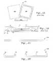
- FIG. 5various views of completed QFN-type (on the left, 501 , 503 , 505 ) and DFN-type (on the right, 551 , 553 , 555 ) packages fabricated in accord with exemplary embodiments of the present invention described herein are shown.
- Top views 501 , 551 , side views 503 , 553 , and bottom views 505 , 555are given to visualize completed packages with reference to QFN-type and DFN-type packages respectively.
- a thermal enhancement of each of the package typesis achieved by having a bottom portion of the die attach paddle exposed.
- the die attach paddlethus arranged provides an efficient conductive thermal path when soldered directly to a PCB.
- thermal conductioncan be achieved through, for example, a thermally-conductive epoxy as well.
- This thermal enhancementcan additionally provide a stable ground by use of down bonds or by electrical connection through a conductive die attach material.
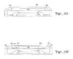
- an integrated circuit die 601is attached directly over a sigulated package 300 ( FIG. 3A ).
- the integrated circuit die 601is electrically attached to the singulated package by a plurality of bonding wires 603 .
- An optional encapsulant 605may be added over the integrated circuit die 601 and the plurality of bonding wires 603 .
- the encapsulant 605may be applied by molding or dispensing techniques, both of which are known in the art.
- the encapsulant 605may be translucent such that any optical properties of the integrated circuit die 601 may be accessed through the translucent encapsulant 605 (e.g., an LED, optical laser, or EPROM).
- an integrated circuit die or discrete component 607may be pre-mounted on a circuit substrate (e.g., a small daughterboard). Additionally, one or more optional discrete components 611 may be mounted to the circuitry substrate 609 .
- the integrated circuit die or discrete component 607 and the one or more optional discrete components 611are electrically connected to the circuitry substrate 609 by a plurality of substrate bonding wires 613 or direct electrical connections (not shown) to the circuitry substrate 609 .
- the circuitry substrate 609is electrically connected to the singulated package by a plurality of package bonding wires 615 .
- An optional encapsulant 617may be added over the integrated circuit die or discrete component 607 , the one or more optional discrete components 611 , the circuitry substrate 609 , and the plurality of bonding wire 613 , 615 .
- the encapsulant 617may be applied by molding or dispensing techniques, both of which are know in the art.
- the encapsulant 617may be translucent such that any optical properties of the integrated circuit die or discrete components 607 , 611 may be accessed through the translucent encapsulant 617 (e.g., and LED, optical laser, or EPROM).
Landscapes
- Engineering & Computer Science (AREA)
- Microelectronics & Electronic Packaging (AREA)
- Power Engineering (AREA)
- Computer Hardware Design (AREA)
- Physics & Mathematics (AREA)
- Condensed Matter Physics & Semiconductors (AREA)
- General Physics & Mathematics (AREA)
- Manufacturing & Machinery (AREA)
- Lead Frames For Integrated Circuits (AREA)
- Die Bonding (AREA)
Abstract
Description
- The invention relates to a three-dimensional stackable semiconductor package, and more particularly, to a three-dimensional stackable semiconductor package for package types involving no-lead packages.
- As semiconductor integrated circuit chips become more multi-functional and highly integrated, the chips include more bonding pads (or terminal pads), and thus packages for the chips have more external terminals (or leads). When a conventional plastic package having leads along the perimeter of the package must accommodate a large number of electrical connection points, the footprint of the package increases. However, a goal in many electronic systems is to minimize an overall size of the systems. Thus, to accommodate a large number of pins without increasing the footprint of package, pin pitch (or lead pitch) of the package must decrease. However, a pin pitch of less that about 0.4 mm gives rise to many technical concerns. For example, trimming of a package having a pin pitch less than 0.4 mm requires expensive trimming tools, and the leads are prone to bending during handling of the package. In addition, surface-mounting of such packages demands a costly and complicated surface-mounting process due to a required critical alignment step.
- Thus, to avoid technical problems associated with conventional fine-pitch packages, packages that have area array or leadless external terminals have been suggested. Among these packages are ball grid array packages, chip scale packages, Quad Flat-Pack No-Lead (QFN) packages, and Dual Flat-Pack No-Lead (DFN) packages. The semiconductor industry presently uses a number of chip scale packages. A micro ball grid array package (μBGA) and a bump chip carrier (BCC) are examples of the chip scale packages. The μBGA package includes a polyimide tape on which a conductive pattern is formed and employs a totally different manufacturing process from a conventional plastic packaging. The bump chip carrier package includes a substrate having grooves formed around a central portion of a top surface of a copper alloy plate and an electroplating layer formed in the groves. Accordingly, chip scale packages use specialized packaging materials and processes that increase package manufacturing costs.
FIG. 1A is a typical plastic encapsulatedpackage 100 of the prior art (showing top100A,bottom 100B, and side views100C of the package). Specifically, the encapsulatedpackage 100 is a QFN package. TheQFN package 100 is a leadless package where electrical contact to a printed circuit board (PCB) is made by soldering lands on thebottom 100B surface of thepackage 100 to the PCB, instead of more traditional formed perimeter leads being soldered to the PCB.FIG. 1B is a cross-sectional view of the priorart QFN package 100 in use and includes acopper land 101, a plurality ofsolder plating areas 103, a plurality ofgold lead wires 105, and a down bond area107. Thecopper land 101 frequently has a platingmaterial 115 applied, such as silver, to facilitate gold or aluminum wire bonding (not shown). An integrated circuit die109 is attached to theQFN package 100 with a suitabledie attach material 113, such as a thermal epoxy. Amold compound 111 or other covering material is applied to finalize theQFN package 100.- Therefore, an integrated circuit package such as a QFN or DFN that uses conventional packaging materials and processes can only be accessed for electrical interconnection, for example, to a printed circuit board, by lower portions of the
copper leadframe 101/plating area103 (FIG. 1B ) which are found only on the bottom surface of the package. Consequently, what is needed to provide for a higher density of integrated circuit packaging into a given printed circuit board footprint is a means of allowing the integrated circuit packages to be readily stacked, one atop another, or even side-by-side. - In one exemplary embodiment, the present invention is a substrate strip component of a leadless three-dimensional stackable semiconductor package having mounting contracts on, for example, top, bottom, and sides of four peripheral edges. The substrate strip may either be fabricated for mounting a single electrical component (e.g., an integrated circuit die) or a plurality of substrate strips may be laid out in an X-Y matrix pattern. The matrix of strips may later be singulated into individual package strips for leadless packages.
- Each of the substrate strips includes a leadless outer portion having a plurality of sections electrically isolated from each other. Each of the sections has a flat wire bonding area and a sidewall area that is essentially perpendicular to the flat wire bonding area. The sidewall area is concentrically located on an outermost periphery of the outer portion.
- Each substrate strip also includes an inner portion located concentrically within and electrically isolated from the outer portion. The inner portion is thinner than the sidewall area of the outer portion and is designed to serve as an attachment area for an integrated circuit die or other electrical component. A combined thickness of the inner portion and the integrated circuit die (or component) is less than a height of the sidewall area. This mounting arrangement leaves an uppermost portion of the sidewall areas electrically exposed for mounting additional leadless packages or other components on top of the first package.
- In another exemplary embodiment, a substrate strip component of a leadless three-dimensional stackable semiconductor package has mounting contacts on, for example, top, bottom, and sides of two opposing (e.g., parallel) edges. The substrate strip may either be fabricated for mounting a single electrical component (e.g., an integrated circuit die) or a plurality of substrate strips may be laid out in an X-Y matrix pattern. The matrix of strips may later be singulated into individual package strip for leadless packages.
- In this embodiment, the substrate strip has a pair of parallel leadless outer portions. Each leadless outer portion has a plurality of sections electrically isolated from each other. Each section also has a flat wire bonding area and a sidewall area essentially perpendicular to the flat wire bonding area, the sidewall area being located on an outermost edge of each of the outer portions.
- An inner portion is located between and electrically isolated from the pair of outer portions. The inner portion is thinner than the sidewall area of the parallel outer portions and is designed to serve as an attachment area for an integrated circuit die or other electrical component. A combined thickness of the inner portion and the integrated circuit die (or component) is less than a height of the sidewall area. This mounting arrangement leaves an uppermost portion of the sidewall areas electrically exposed for mounting additional leadless packages or other components on top of the first package.
- In another exemplary embodiment, the present invention is a method of packaging a semiconductor device. The method includes mounting an electrical component to an inner portion die pad where the die pad is a portion of a substrate strip component of a first leadless three-dimensional stackable semiconductor package. A plurality of bond wires is secured from a plurality of bond pads on the electrical component to corresponding ones of a plurality of wirebond pads contained on a leadless outer portion of the substrate strip component. The outer portion has a sidewall that has a height greater than a combined height of the electrical component and the inner portion die pad.
- The electrical component, bond wires, and any exposed portions of the die pad are then covered with an encapsulating material to a level at or near the uppermost portion of the sidewalls on the leadless outer portion.
FIGS. 1A and 1B show a QFN chip carrier package of the prior art.FIGS. 2A-2F show exemplary cross-sections or plan views of stackable integrated circuit die and discrete component carriers in accord with the present invention.FIGS. 3A and 3B show singulated packages in single and stacked configurations.FIGS. 4A-4D show various cross-sectional embodiments allowing for differing arrangements of layouts for singulation.FIG. 5 shows completed exterior views of specific embodiments of QFN and DFN packages in accord with general embodiments of the present invention.FIGS. 6A and 6B show singulated packages stacked with separate integrated circuit dice and discrete components.- In
FIG. 2A , asubstrate strip 201A is selected to have a thickness close to a final “height” of a completed package. The height chosen for thesubstrate strip 201A will be based on particular components placed in the final package but will typically vary from 0.2 mm to 2 mm. Additional details to determine an actual height for a given package will be discussed in greater detail, infra. - Processes described herein refer to exemplary embodiments where many packages are formed in an X-Y matrix, although a single package could readily be formed by the same process as well. The X-Y matrix size for the
substrate strip 201A may be chosen to suit a particular vendor's tooling. In a specific exemplary embodiment, the X-Y dimensions of the substrate may be 205 mm×60 mm and the construction material is selected to be copper. In other exemplary embodiments, thesubstrate 201A may be another type of metallic or non-metallic material. The material may be either electrically conductive or electrically non-conductive. Additionally, non-rectangular matrix shapes are contemplated. - In
FIG. 2B , thesubstrate strip 201A is pattern-etched, leaving anetched substrate strip 201B. During the pattern-etching process, a bottom thickness of thesubstrate strip 201A is reduced while leaving essentiallyfull height sidewalls 203. Pattern forming and pattern-etching steps are known in the art and will vary depending upon material chosen. Areas between thesidewalls 203 are reduced thickness areas. Portions of these areas will serve as a die pad mounting area in subsequent steps. Thus, thesidewalls 203 are areas substantially perpendicular to the reduced thickness areas. A height of the sidewalls is selected to be sufficient such that any mounted integrated circuit and bonding leads contained within the package will be at or below an uppermost portion of thesidewalls 203. Other portions of the bottom thickness will later serve as bond fingers. In a specific exemplary embodiment, bottom portions of the etchedsubstrate strip 201B are reduced to about 0.12 mm (approximately 5 mils) in height. - With reference to
FIG. 2C , the etchedsubstrate strip 201B is further pattern-etched forming a leadframe substrate strip201C. The leadframe substrate strip201C includes die attachpads 205 and thesidewalls 203 are further etched defining separate bond finger features as seen in plan-view 207. The plan-view 207 shows a portion of the exemplary 205 mm×60 mm substrate. As viewed jointly in cross-sectional and plan-view, the bond fingers haveintegral sidewalls 203 which remain substantially the full height of the leadframe substrate strip201C. The die attachpads 205 are electrically isolated from the bond finger/integral sidewalls 203 due to the pattern-etch step. In a specific exemplary embodiment, exposed areas of the leadframe substrate strip201C are either fully-plated or spot-plated with, for example, silver. In other exemplary embodiments, the leadframe substrate strip201C is fully plated with a wire-bondable metal and solderable metal layers. For example, the leadframe substrate strip201C may be a leadframe with a nickel-palladium-gold (Ni—PD—Au) plating. A high-temperature polyamide tape may be used to secure all package portions in position. - In
FIG. 2D , an etched leadframe substrate strip201D is populated by adhering (e.g., via a standard thermal epoxy or adhesive tape) individual integratedcircuit dice 209 to the die attachpads 205. Various adhering techniques and processes are known in the industry.Bonding wires 211 are then attached to electrically connect to portions of the etched leadframe substrate strip201D. - With reference to
FIG. 2E , apopulated leadframe strip 201E is then encapsulated with anepoxy mold compound 213. Encapsulation techniques are well-known in the art. After encapsulation, exposed portions of thepopulated leadframe strip 201E are then plated with, for example, tin (Sn), a tin-alloy, Ni/Au or other plating materials possessing characteristics of being electrically-conductive and solderable. The plating allows for good electrical connections when the final package is mounted to a PCB or another die package. If the leadframe substrate strip is pre-plated, this final plating step is unnecessary. - In
FIG. 2F , thepopulated leadframe strip 201E is then singulated by standard techniques such as sawing or laser-cutting along a plurality of saw-lines 215. After the singulation process, a plurality of QFN-type packages are produced. Each of thesidewalls 203, which are a full-height integral part of the formed bond finger features (FIG. 2C ) carry an electrical signal from a lower portion of the package to an upper portion of the package. Thus, all electrical signals are available on both upper and lower portions of the final package so three-dimensional stacking of packages is possible. - Alternatively, a skilled artisan can readily envision modifications to the above-described processes wherein DFN-type packages are produced. DFN-type packages have external connection points on two parallel opposing edges of the package rather than on all four edges as with the QFN-type package.
- With reference to
FIG. 3A , a singulated DFN-type or QFN-type package 300 is shown in cross-section. (Note that either the QFN-type or DFN-type package appears similar to the other in cross-section). The singulated DFN-type or QFN-type package 300 can be used as a single package and mounted to a PCB or other structure directly. Alternatively, as shown inFIG. 3B , three singulated DFN-type or QFN-type packages 300 are stacked in a three-dimensional structure 350. Each of thesingulated packages 300 is electrically connected to the other by, for example, solder joints301. FIGS. 4A through 4D indicate alternative embodiments for the substrate strip explained in detail with reference toFIGS. 2A through 2F , supra. A singulation saw401 (or laser or other singulation method) placement provides an indication of some various arrangements of sidewalls. For comparison purposes, a common sidewall approach ofFIG. 4A is the same solid common wall approach described with reference toFIGS. 2A through 2F , supra.FIG. 4B is an alternate configuration for a sidewall design. A “gap” located between the twosingulation saws 401 was formed during the leadframe substrate strip etching process (FIG. 2C ). Leaving the gap results in less metal sidewall for the singulation saw401, thus decreasing sawing time while reducing blade wear.FIG. 4C indicates a wall arrangement where a gap has been left on the underside of the sidewall. Such an arrangement may be achieved by, for example, two-sided etching. Alternatively, the underside gap may be formed by mechanical means such as punching or stamping.- A dual sidewall arrangement of
FIG. 4D is formed similarly to the formation method described with reference toFIG. 4C . - With reference to
FIG. 5 , various views of completed QFN-type (on the left,501,503,505) and DFN-type (on the right,551,553,555) packages fabricated in accord with exemplary embodiments of the present invention described herein are shown.Top views side views bottom views bottom views - In an alternative three-dimensional stacking arrangement of
FIG. 6A , an integrated circuit die601 is attached directly over a sigulated package300 (FIG. 3A ). The integrated circuit die601 is electrically attached to the singulated package by a plurality ofbonding wires 603. Anoptional encapsulant 605 may be added over the integrated circuit die601 and the plurality ofbonding wires 603. Theencapsulant 605 may be applied by molding or dispensing techniques, both of which are known in the art. In a specific exemplary embodiment, theencapsulant 605 may be translucent such that any optical properties of the integrated circuit die601 may be accessed through the translucent encapsulant605 (e.g., an LED, optical laser, or EPROM). - In another alternative stacking arrangement of
FIG. 6B , an integrated circuit die ordiscrete component 607 may be pre-mounted on a circuit substrate (e.g., a small daughterboard). Additionally, one or more optionaldiscrete components 611 may be mounted to thecircuitry substrate 609. The integrated circuit die ordiscrete component 607 and the one or more optionaldiscrete components 611 are electrically connected to thecircuitry substrate 609 by a plurality ofsubstrate bonding wires 613 or direct electrical connections (not shown) to thecircuitry substrate 609. Thecircuitry substrate 609, in turn, is electrically connected to the singulated package by a plurality ofpackage bonding wires 615. Anoptional encapsulant 617 may be added over the integrated circuit die ordiscrete component 607, the one or more optionaldiscrete components 611, thecircuitry substrate 609, and the plurality ofbonding wire encapsulant 617 may be applied by molding or dispensing techniques, both of which are know in the art. In a specific exemplary embodiment, theencapsulant 617 may be translucent such that any optical properties of the integrated circuit die ordiscrete components - In the foregoing specification, the present invention has been described with reference to specific embodiments thereof. It will, however, be evident to a skilled artisan that various modifications and changes can be made thereto without departing from the broader spirit and scope of the invention as set forth in the appended claims. For example, skilled artisans will appreciate that embodiments of the present invention may be readily applied to modified versions of TAPP® (thin array plastic package), ULGA® (ultra-thin land grid array), BCC® (bumped chip carrier), or other similar package types. The specification and drawings are, accordingly, to be regarded in an illustrative rather than a restrictive sense.
Claims (27)
Priority Applications (5)
| Application Number | Priority Date | Filing Date | Title |
|---|---|---|---|
| US11/467,786US7816769B2 (en) | 2006-08-28 | 2006-08-28 | Stackable packages for three-dimensional packaging of semiconductor dice |
| PCT/US2007/075191WO2008027694A2 (en) | 2006-08-28 | 2007-08-03 | Stackable packages for three-dimensional packaging of semiconductor dice |
| CN2007800320099ACN101512762B (en) | 2006-08-28 | 2007-08-03 | Stackable packages for three-dimensional packaging of semiconductor dice |
| TW096130622ATW200818458A (en) | 2006-08-28 | 2007-08-17 | Stackable packages for three-dimensional packaging of semiconductor dice |
| US12/891,386US8278150B2 (en) | 2006-08-28 | 2010-09-27 | Stackable packages for three-dimensional packaging of semiconductor dice |
Applications Claiming Priority (1)
| Application Number | Priority Date | Filing Date | Title |
|---|---|---|---|
| US11/467,786US7816769B2 (en) | 2006-08-28 | 2006-08-28 | Stackable packages for three-dimensional packaging of semiconductor dice |
Related Child Applications (1)
| Application Number | Title | Priority Date | Filing Date |
|---|---|---|---|
| US12/891,386DivisionUS8278150B2 (en) | 2006-08-28 | 2010-09-27 | Stackable packages for three-dimensional packaging of semiconductor dice |
Publications (2)
| Publication Number | Publication Date |
|---|---|
| US20080048308A1true US20080048308A1 (en) | 2008-02-28 |
| US7816769B2 US7816769B2 (en) | 2010-10-19 |
Family
ID=39112593
Family Applications (2)
| Application Number | Title | Priority Date | Filing Date |
|---|---|---|---|
| US11/467,786Active2026-11-28US7816769B2 (en) | 2006-08-28 | 2006-08-28 | Stackable packages for three-dimensional packaging of semiconductor dice |
| US12/891,386Active2027-01-04US8278150B2 (en) | 2006-08-28 | 2010-09-27 | Stackable packages for three-dimensional packaging of semiconductor dice |
Family Applications After (1)
| Application Number | Title | Priority Date | Filing Date |
|---|---|---|---|
| US12/891,386Active2027-01-04US8278150B2 (en) | 2006-08-28 | 2010-09-27 | Stackable packages for three-dimensional packaging of semiconductor dice |
Country Status (4)
| Country | Link |
|---|---|
| US (2) | US7816769B2 (en) |
| CN (1) | CN101512762B (en) |
| TW (1) | TW200818458A (en) |
| WO (1) | WO2008027694A2 (en) |
Cited By (52)
| Publication number | Priority date | Publication date | Assignee | Title |
|---|---|---|---|---|
| US20080099784A1 (en)* | 2006-10-31 | 2008-05-01 | Wai Yew Lo | Array quad flat no-lead package and method of forming same |
| DE102008014927A1 (en)* | 2008-02-22 | 2009-08-27 | Osram Opto Semiconductors Gmbh | Method for producing a plurality of radiation-emitting components and radiation-emitting component |
| US20090282782A1 (en)* | 2008-05-15 | 2009-11-19 | Xerox Corporation | System and method for automating package assembly |
| US20100110479A1 (en)* | 2008-11-06 | 2010-05-06 | Xerox Corporation | Packaging digital front end |
| US20100123237A1 (en)* | 2008-11-18 | 2010-05-20 | Samsung Electronics Co., Ltd. | Semiconductor package of multi stack type |
| US20100149597A1 (en)* | 2008-12-16 | 2010-06-17 | Xerox Corporation | System and method to derive structure from image |
| US20100222908A1 (en)* | 2009-02-27 | 2010-09-02 | Xerox Corporation | Package generation system |
| US7790512B1 (en) | 2007-11-06 | 2010-09-07 | Utac Thai Limited | Molded leadframe substrate semiconductor package |
| US20100230802A1 (en)* | 2009-03-12 | 2010-09-16 | Utac Thai Limited | Metallic solderability preservation coating on metal part of semiconductor package to prevent oxide |
| US20100311208A1 (en)* | 2008-05-22 | 2010-12-09 | Utac Thai Limited | Method and apparatus for no lead semiconductor package |
| US20100327432A1 (en)* | 2006-09-26 | 2010-12-30 | Utac Thai Limited | Package with heat transfer |
| US20110014747A1 (en)* | 2006-08-28 | 2011-01-20 | Atmel Corporation | Stackable packages for three-dimensional packaging of semiconductor dice |
| US20110039371A1 (en)* | 2008-09-04 | 2011-02-17 | Utac Thai Limited | Flip chip cavity package |
| US20110054849A1 (en)* | 2009-08-27 | 2011-03-03 | Xerox Corporation | System for automatically generating package designs and concepts |
| US20110076805A1 (en)* | 2006-12-14 | 2011-03-31 | Utac Thai Limited | Molded leadframe substrate semiconductor package |
| US20110119570A1 (en)* | 2009-11-18 | 2011-05-19 | Xerox Corporation | Automated variable dimension digital document advisor |
| US20110133319A1 (en)* | 2009-12-04 | 2011-06-09 | Utac Thai Limited | Auxiliary leadframe member for stabilizing the bond wire process |
| US20110147931A1 (en)* | 2006-04-28 | 2011-06-23 | Utac Thai Limited | Lead frame land grid array with routing connector trace under unit |
| US20110198752A1 (en)* | 2006-04-28 | 2011-08-18 | Utac Thai Limited | Lead frame ball grid array with traces under die |
| US8013437B1 (en) | 2006-09-26 | 2011-09-06 | Utac Thai Limited | Package with heat transfer |
| US20110221051A1 (en)* | 2010-03-11 | 2011-09-15 | Utac Thai Limited | Leadframe based multi terminal ic package |
| US20120040498A1 (en)* | 2008-07-23 | 2012-02-16 | Samsung Electronics Co., Ltd | Semiconductor device package and method of fabricating the same |
| US8160992B2 (en) | 2008-05-15 | 2012-04-17 | Xerox Corporation | System and method for selecting a package structural design |
| US8310060B1 (en) | 2006-04-28 | 2012-11-13 | Utac Thai Limited | Lead frame land grid array |
| US8334764B1 (en) | 2008-12-17 | 2012-12-18 | Utac Thai Limited | Method and apparatus to prevent double semiconductor units in test socket |
| CN103000608A (en)* | 2012-12-11 | 2013-03-27 | 矽力杰半导体技术(杭州)有限公司 | Chip packaging structure of a plurality of assemblies |
| US8461694B1 (en) | 2006-04-28 | 2013-06-11 | Utac Thai Limited | Lead frame ball grid array with traces under die having interlocking features |
| US8460970B1 (en) | 2006-04-28 | 2013-06-11 | Utac Thai Limited | Lead frame ball grid array with traces under die having interlocking features |
| US8643874B2 (en) | 2009-12-18 | 2014-02-04 | Xerox Corporation | Method and system for generating a workflow to produce a dimensional document |
| US8757479B2 (en) | 2012-07-31 | 2014-06-24 | Xerox Corporation | Method and system for creating personalized packaging |
| US8871571B2 (en) | 2010-04-02 | 2014-10-28 | Utac Thai Limited | Apparatus for and methods of attaching heat slugs to package tops |
| US9000590B2 (en) | 2012-05-10 | 2015-04-07 | Utac Thai Limited | Protruding terminals with internal routing interconnections semiconductor device |
| US9006034B1 (en) | 2012-06-11 | 2015-04-14 | Utac Thai Limited | Post-mold for semiconductor package having exposed traces |
| US9082207B2 (en) | 2009-11-18 | 2015-07-14 | Xerox Corporation | System and method for automatic layout of printed material on a three-dimensional structure |
| US9132599B2 (en) | 2008-09-05 | 2015-09-15 | Xerox Corporation | System and method for image registration for packaging |
| US20160049526A1 (en)* | 2014-08-18 | 2016-02-18 | Optiz, Inc. | Wire Bond Sensor Package And Method |
| US9355940B1 (en) | 2009-12-04 | 2016-05-31 | Utac Thai Limited | Auxiliary leadframe member for stabilizing the bond wire process |
| US9449905B2 (en) | 2012-05-10 | 2016-09-20 | Utac Thai Limited | Plated terminals with routing interconnections semiconductor device |
| US9449900B2 (en) | 2009-07-23 | 2016-09-20 | UTAC Headquarters Pte. Ltd. | Leadframe feature to minimize flip-chip semiconductor die collapse during flip-chip reflow |
| US9761435B1 (en) | 2006-12-14 | 2017-09-12 | Utac Thai Limited | Flip chip cavity package |
| US9760659B2 (en) | 2014-01-30 | 2017-09-12 | Xerox Corporation | Package definition system with non-symmetric functional elements as a function of package edge property |
| US20170294367A1 (en)* | 2016-04-07 | 2017-10-12 | Microchip Technology Incorporated | Flat No-Leads Package With Improved Contact Pins |
| US9805955B1 (en) | 2015-11-10 | 2017-10-31 | UTAC Headquarters Pte. Ltd. | Semiconductor package with multiple molding routing layers and a method of manufacturing the same |
| US9892212B2 (en) | 2014-05-19 | 2018-02-13 | Xerox Corporation | Creation of variable cut files for package design |
| US9916401B2 (en) | 2015-05-18 | 2018-03-13 | Xerox Corporation | Creation of cut files for personalized package design using multiple substrates |
| US9916402B2 (en) | 2015-05-18 | 2018-03-13 | Xerox Corporation | Creation of cut files to fit a large package flat on one or more substrates |
| CN108417556A (en)* | 2018-05-23 | 2018-08-17 | 奥肯思(北京)科技有限公司 | Multichip stacking encapsulation structure |
| US10242953B1 (en) | 2015-05-27 | 2019-03-26 | Utac Headquarters PTE. Ltd | Semiconductor package with plated metal shielding and a method thereof |
| US10242934B1 (en) | 2014-05-07 | 2019-03-26 | Utac Headquarters Pte Ltd. | Semiconductor package with full plating on contact side surfaces and methods thereof |
| US10276477B1 (en) | 2016-05-20 | 2019-04-30 | UTAC Headquarters Pte. Ltd. | Semiconductor package with multiple stacked leadframes and a method of manufacturing the same |
| US20190221502A1 (en)* | 2018-01-17 | 2019-07-18 | Microchip Technology Incorporated | Down Bond in Semiconductor Devices |
| US20220310502A1 (en)* | 2021-03-26 | 2022-09-29 | Taiwan Semiconductor Manufacturing Company, Ltd. | Semiconductor device and manufacturing method thereof |
Families Citing this family (17)
| Publication number | Priority date | Publication date | Assignee | Title |
|---|---|---|---|---|
| JP2009094118A (en)* | 2007-10-04 | 2009-04-30 | Panasonic Corp | Lead frame, electronic component including the same, and manufacturing method thereof |
| CN102194770A (en)* | 2010-03-08 | 2011-09-21 | 优特泰国有限公司 | Ultrathin semiconductor package |
| TWI555150B (en) | 2014-05-27 | 2016-10-21 | 財團法人工業技術研究院 | Electronic components and their methods |
| DE102014107729B4 (en)* | 2014-06-02 | 2022-05-12 | Infineon Technologies Ag | Three-dimensional stack of a leaded package and an electronic element and method of making such a stack |
| CN105161425A (en)* | 2015-07-30 | 2015-12-16 | 南通富士通微电子股份有限公司 | Semiconductor stacked packaging method |
| CN105161424A (en)* | 2015-07-30 | 2015-12-16 | 南通富士通微电子股份有限公司 | Semiconductor stacked packaging method |
| CN105097569A (en)* | 2015-07-30 | 2015-11-25 | 南通富士通微电子股份有限公司 | Semiconductor lamination packaging method |
| JP6716363B2 (en)* | 2016-06-28 | 2020-07-01 | 株式会社アムコー・テクノロジー・ジャパン | Semiconductor package and manufacturing method thereof |
| JP6610497B2 (en)* | 2016-10-14 | 2019-11-27 | オムロン株式会社 | Electronic device and manufacturing method thereof |
| CN108206170B (en)* | 2017-12-29 | 2020-03-06 | 江苏长电科技股份有限公司 | Semiconductor package structure with pin sidewall creeping tin function and its manufacturing process |
| CN108198804B (en)* | 2017-12-29 | 2020-03-06 | 江苏长电科技股份有限公司 | Stacked package structure with pin sidewall climbing tin function and its manufacturing process |
| CN108198797B (en)* | 2017-12-29 | 2020-03-06 | 江苏长电科技股份有限公司 | Semiconductor package structure with pin sidewall creeping tin function and its manufacturing process |
| CN108109972B (en)* | 2017-12-29 | 2020-03-06 | 江苏长电科技股份有限公司 | Semiconductor package structure with pin sidewall creeping tin function and its manufacturing process |
| CN108198761B (en)* | 2017-12-29 | 2020-06-09 | 江苏长电科技股份有限公司 | Semiconductor package structure with pin sidewall creeping tin function and its manufacturing process |
| CN108198790B (en)* | 2017-12-29 | 2020-03-06 | 江苏长电科技股份有限公司 | Stacked package structure with pin sidewall climbing tin function and its manufacturing process |
| US11145578B2 (en)* | 2019-09-24 | 2021-10-12 | Infineon Technologies Ag | Semiconductor package with top or bottom side cooling and method for manufacturing the semiconductor package |
| CN116282841B (en)* | 2023-03-31 | 2024-10-18 | 四川虹科创新科技有限公司 | Dust deposition structure of rotary flashboard for cleaning glass kiln |
Citations (20)
| Publication number | Priority date | Publication date | Assignee | Title |
|---|---|---|---|---|
| US5157475A (en)* | 1988-07-08 | 1992-10-20 | Oki Electric Industry Co., Ltd. | Semiconductor device having a particular conductive lead structure |
| US5422514A (en)* | 1993-05-11 | 1995-06-06 | Micromodule Systems, Inc. | Packaging and interconnect system for integrated circuits |
| US5541449A (en)* | 1994-03-11 | 1996-07-30 | The Panda Project | Semiconductor chip carrier affording a high-density external interface |
| US5585675A (en)* | 1994-05-11 | 1996-12-17 | Harris Corporation | Semiconductor die packaging tub having angularly offset pad-to-pad via structure configured to allow three-dimensional stacking and electrical interconnections among multiple identical tubs |
| US5744827A (en)* | 1995-11-28 | 1998-04-28 | Samsung Electronics Co., Ltd. | Three dimensional stack package device having exposed coupling lead portions and vertical interconnection elements |
| US5804874A (en)* | 1996-03-08 | 1998-09-08 | Samsung Electronics Co., Ltd. | Stacked chip package device employing a plurality of lead on chip type semiconductor chips |
| US5835988A (en)* | 1996-03-27 | 1998-11-10 | Mitsubishi Denki Kabushiki Kaisha | Packed semiconductor device with wrap around external leads |
| US6061251A (en)* | 1997-09-08 | 2000-05-09 | Hewlett-Packard Company | Lead-frame based vertical interconnect package |
| US6294407B1 (en)* | 1998-05-06 | 2001-09-25 | Virtual Integration, Inc. | Microelectronic packages including thin film decal and dielectric adhesive layer having conductive vias therein, and methods of fabricating the same |
| US6320251B1 (en)* | 2000-01-18 | 2001-11-20 | Amkor Technology, Inc. | Stackable package for an integrated circuit |
| US6339255B1 (en)* | 1998-10-24 | 2002-01-15 | Hyundai Electronics Industries Co., Ltd. | Stacked semiconductor chips in a single semiconductor package |
| US6414391B1 (en)* | 1998-06-30 | 2002-07-02 | Micron Technology, Inc. | Module assembly for stacked BGA packages with a common bus bar in the assembly |
| US6525406B1 (en)* | 1999-10-15 | 2003-02-25 | Amkor Technology, Inc. | Semiconductor device having increased moisture path and increased solder joint strength |
| US6667544B1 (en)* | 2000-06-30 | 2003-12-23 | Amkor Technology, Inc. | Stackable package having clips for fastening package and tool for opening clips |
| US6674159B1 (en)* | 2000-05-16 | 2004-01-06 | Sandia National Laboratories | Bi-level microelectronic device package with an integral window |
| US6710246B1 (en)* | 2002-08-02 | 2004-03-23 | National Semiconductor Corporation | Apparatus and method of manufacturing a stackable package for a semiconductor device |
| US6812552B2 (en)* | 2002-04-29 | 2004-11-02 | Advanced Interconnect Technologies Limited | Partially patterned lead frames and methods of making and using the same in semiconductor packaging |
| US20050067680A1 (en)* | 2003-09-30 | 2005-03-31 | Boon Suan Jeung | Castellated chip-scale packages and methods for fabricating the same |
| US20060027908A1 (en)* | 2004-08-03 | 2006-02-09 | Shu-Ming Chang | 3-D stackable semiconductor package |
| US7385299B2 (en)* | 2006-02-25 | 2008-06-10 | Stats Chippac Ltd. | Stackable integrated circuit package system with multiple interconnect interface |
Family Cites Families (11)
| Publication number | Priority date | Publication date | Assignee | Title |
|---|---|---|---|---|
| US6281568B1 (en)* | 1998-10-21 | 2001-08-28 | Amkor Technology, Inc. | Plastic integrated circuit device package and leadframe having partially undercut leads and die pad |
| DE10031204A1 (en)* | 2000-06-27 | 2002-01-17 | Infineon Technologies Ag | System carrier for semiconductor chips and electronic components and manufacturing method for a system carrier and for electronic components |
| CN1207784C (en)* | 2001-04-16 | 2005-06-22 | 矽品精密工业股份有限公司 | Cross-stacked two-chip packaging device and manufacturing method |
| CN2613047Y (en) | 2003-03-11 | 2004-04-21 | 胜开科技股份有限公司 | IC stack package assembly |
| CN101587869B (en) | 2003-08-26 | 2011-04-13 | 宇芯(毛里求斯)控股有限公司 | Reversible leadless package and methods of making and using same |
| US7122406B1 (en)* | 2004-01-02 | 2006-10-17 | Gem Services, Inc. | Semiconductor device package diepad having features formed by electroplating |
| US7129569B2 (en)* | 2004-04-30 | 2006-10-31 | St Assembly Test Services Ltd. | Large die package structures and fabrication method therefor |
| WO2007005263A2 (en)* | 2005-06-30 | 2007-01-11 | Fairchild Semiconductor Corporation | Semiconductor die package and method for making the same |
| MY142210A (en)* | 2006-06-05 | 2010-11-15 | Carsem M Sdn Bhd | Multiple row exposed leads for mlp high density packages |
| WO2008024769A2 (en) | 2006-08-21 | 2008-02-28 | Raven Biotechnologies, Inc. | Intensified perfusion production method |
| US7816769B2 (en) | 2006-08-28 | 2010-10-19 | Atmel Corporation | Stackable packages for three-dimensional packaging of semiconductor dice |
- 2006
- 2006-08-28USUS11/467,786patent/US7816769B2/enactiveActive
- 2007
- 2007-08-03WOPCT/US2007/075191patent/WO2008027694A2/enactiveApplication Filing
- 2007-08-03CNCN2007800320099Apatent/CN101512762B/ennot_activeExpired - Fee Related
- 2007-08-17TWTW096130622Apatent/TW200818458A/enunknown
- 2010
- 2010-09-27USUS12/891,386patent/US8278150B2/enactiveActive
Patent Citations (28)
| Publication number | Priority date | Publication date | Assignee | Title |
|---|---|---|---|---|
| US5157475A (en)* | 1988-07-08 | 1992-10-20 | Oki Electric Industry Co., Ltd. | Semiconductor device having a particular conductive lead structure |
| US5422514A (en)* | 1993-05-11 | 1995-06-06 | Micromodule Systems, Inc. | Packaging and interconnect system for integrated circuits |
| US5541449A (en)* | 1994-03-11 | 1996-07-30 | The Panda Project | Semiconductor chip carrier affording a high-density external interface |
| US5585675A (en)* | 1994-05-11 | 1996-12-17 | Harris Corporation | Semiconductor die packaging tub having angularly offset pad-to-pad via structure configured to allow three-dimensional stacking and electrical interconnections among multiple identical tubs |
| US5744827A (en)* | 1995-11-28 | 1998-04-28 | Samsung Electronics Co., Ltd. | Three dimensional stack package device having exposed coupling lead portions and vertical interconnection elements |
| US5804874A (en)* | 1996-03-08 | 1998-09-08 | Samsung Electronics Co., Ltd. | Stacked chip package device employing a plurality of lead on chip type semiconductor chips |
| US5835988A (en)* | 1996-03-27 | 1998-11-10 | Mitsubishi Denki Kabushiki Kaisha | Packed semiconductor device with wrap around external leads |
| US6061251A (en)* | 1997-09-08 | 2000-05-09 | Hewlett-Packard Company | Lead-frame based vertical interconnect package |
| US6294407B1 (en)* | 1998-05-06 | 2001-09-25 | Virtual Integration, Inc. | Microelectronic packages including thin film decal and dielectric adhesive layer having conductive vias therein, and methods of fabricating the same |
| US20030038378A1 (en)* | 1998-05-06 | 2003-02-27 | Virtual Integration, Inc. | Microelectronic packages including thin film decal and dielectric adhesive layer having conductive vias therein |
| US20050110135A1 (en)* | 1998-06-30 | 2005-05-26 | Corisis David J. | Module assembly and method for stacked BGA packages |
| US6838768B2 (en)* | 1998-06-30 | 2005-01-04 | Micron Technology Inc | Module assembly for stacked BGA packages |
| US20030197271A1 (en)* | 1998-06-30 | 2003-10-23 | Corisis David J. | Module assembly for stacked BGA packages |
| US6414391B1 (en)* | 1998-06-30 | 2002-07-02 | Micron Technology, Inc. | Module assembly for stacked BGA packages with a common bus bar in the assembly |
| US20020125571A1 (en)* | 1998-06-30 | 2002-09-12 | Corisis David J. | Module assembly for stacked BGA packages |
| US6563217B2 (en)* | 1998-06-30 | 2003-05-13 | Micron Technology, Inc. | Module assembly for stacked BGA packages |
| US6500698B2 (en)* | 1998-10-24 | 2002-12-31 | Hynix Semiconductor, Inc. | Method for fabricating a stacked semiconductor chip package |
| US20020022300A1 (en)* | 1998-10-24 | 2002-02-21 | Hyundai Electronics Industries Co., Ltd. | Method for fabricating a stacked semiconductor chip package |
| US6339255B1 (en)* | 1998-10-24 | 2002-01-15 | Hyundai Electronics Industries Co., Ltd. | Stacked semiconductor chips in a single semiconductor package |
| US6525406B1 (en)* | 1999-10-15 | 2003-02-25 | Amkor Technology, Inc. | Semiconductor device having increased moisture path and increased solder joint strength |
| US6320251B1 (en)* | 2000-01-18 | 2001-11-20 | Amkor Technology, Inc. | Stackable package for an integrated circuit |
| US6674159B1 (en)* | 2000-05-16 | 2004-01-06 | Sandia National Laboratories | Bi-level microelectronic device package with an integral window |
| US6667544B1 (en)* | 2000-06-30 | 2003-12-23 | Amkor Technology, Inc. | Stackable package having clips for fastening package and tool for opening clips |
| US6812552B2 (en)* | 2002-04-29 | 2004-11-02 | Advanced Interconnect Technologies Limited | Partially patterned lead frames and methods of making and using the same in semiconductor packaging |
| US6710246B1 (en)* | 2002-08-02 | 2004-03-23 | National Semiconductor Corporation | Apparatus and method of manufacturing a stackable package for a semiconductor device |
| US20050067680A1 (en)* | 2003-09-30 | 2005-03-31 | Boon Suan Jeung | Castellated chip-scale packages and methods for fabricating the same |
| US20060027908A1 (en)* | 2004-08-03 | 2006-02-09 | Shu-Ming Chang | 3-D stackable semiconductor package |
| US7385299B2 (en)* | 2006-02-25 | 2008-06-10 | Stats Chippac Ltd. | Stackable integrated circuit package system with multiple interconnect interface |
Cited By (101)
| Publication number | Priority date | Publication date | Assignee | Title |
|---|---|---|---|---|
| US8492906B2 (en) | 2006-04-28 | 2013-07-23 | Utac Thai Limited | Lead frame ball grid array with traces under die |
| US8460970B1 (en) | 2006-04-28 | 2013-06-11 | Utac Thai Limited | Lead frame ball grid array with traces under die having interlocking features |
| US20110198752A1 (en)* | 2006-04-28 | 2011-08-18 | Utac Thai Limited | Lead frame ball grid array with traces under die |
| US8487451B2 (en) | 2006-04-28 | 2013-07-16 | Utac Thai Limited | Lead frame land grid array with routing connector trace under unit |
| US8704381B2 (en) | 2006-04-28 | 2014-04-22 | Utac Thai Limited | Very extremely thin semiconductor package |
| US8685794B2 (en) | 2006-04-28 | 2014-04-01 | Utac Thai Limited | Lead frame land grid array with routing connector trace under unit |
| US8652879B2 (en) | 2006-04-28 | 2014-02-18 | Utac Thai Limited | Lead frame ball grid array with traces under die |
| US8575762B2 (en) | 2006-04-28 | 2013-11-05 | Utac Thai Limited | Very extremely thin semiconductor package |
| US8310060B1 (en) | 2006-04-28 | 2012-11-13 | Utac Thai Limited | Lead frame land grid array |
| US20110147931A1 (en)* | 2006-04-28 | 2011-06-23 | Utac Thai Limited | Lead frame land grid array with routing connector trace under unit |
| US9099317B2 (en) | 2006-04-28 | 2015-08-04 | Utac Thai Limited | Method for forming lead frame land grid array |
| US8461694B1 (en) | 2006-04-28 | 2013-06-11 | Utac Thai Limited | Lead frame ball grid array with traces under die having interlocking features |
| US20110014747A1 (en)* | 2006-08-28 | 2011-01-20 | Atmel Corporation | Stackable packages for three-dimensional packaging of semiconductor dice |
| US8278150B2 (en) | 2006-08-28 | 2012-10-02 | Atmel Corporation | Stackable packages for three-dimensional packaging of semiconductor dice |
| US20100327432A1 (en)* | 2006-09-26 | 2010-12-30 | Utac Thai Limited | Package with heat transfer |
| US8125077B2 (en) | 2006-09-26 | 2012-02-28 | Utac Thai Limited | Package with heat transfer |
| US8013437B1 (en) | 2006-09-26 | 2011-09-06 | Utac Thai Limited | Package with heat transfer |
| US7531383B2 (en)* | 2006-10-31 | 2009-05-12 | Freescale Semiconductor, Inc. | Array quad flat no-lead package and method of forming same |
| US20080099784A1 (en)* | 2006-10-31 | 2008-05-01 | Wai Yew Lo | Array quad flat no-lead package and method of forming same |
| US9761435B1 (en) | 2006-12-14 | 2017-09-12 | Utac Thai Limited | Flip chip cavity package |
| US9099294B1 (en)* | 2006-12-14 | 2015-08-04 | Utac Thai Limited | Molded leadframe substrate semiconductor package |
| US20110076805A1 (en)* | 2006-12-14 | 2011-03-31 | Utac Thai Limited | Molded leadframe substrate semiconductor package |
| US9196470B1 (en)* | 2006-12-14 | 2015-11-24 | Utac Thai Limited | Molded leadframe substrate semiconductor package |
| US9093486B2 (en) | 2006-12-14 | 2015-07-28 | Utac Thai Limited | Molded leadframe substrate semiconductor package |
| US9711343B1 (en)* | 2006-12-14 | 2017-07-18 | Utac Thai Limited | Molded leadframe substrate semiconductor package |
| US9082607B1 (en) | 2006-12-14 | 2015-07-14 | Utac Thai Limited | Molded leadframe substrate semiconductor package |
| US9899208B2 (en) | 2006-12-14 | 2018-02-20 | Utac Thai Limited | Molded leadframe substrate semiconductor package |
| US8338922B1 (en) | 2007-11-06 | 2012-12-25 | Utac Thai Limited | Molded leadframe substrate semiconductor package |
| US7790512B1 (en) | 2007-11-06 | 2010-09-07 | Utac Thai Limited | Molded leadframe substrate semiconductor package |
| US8790939B2 (en) | 2008-02-22 | 2014-07-29 | Osram Opto Semiconductors Gmbh | Method for producing a plurality of radiation-emitting components and radiation-emitting component |
| US20110127564A1 (en)* | 2008-02-22 | 2011-06-02 | Osram Opto Semiconductors Gmbh | Method for producing a plurality of radiation-emitting components and radiation-emitting component |
| DE102008014927A1 (en)* | 2008-02-22 | 2009-08-27 | Osram Opto Semiconductors Gmbh | Method for producing a plurality of radiation-emitting components and radiation-emitting component |
| US8160992B2 (en) | 2008-05-15 | 2012-04-17 | Xerox Corporation | System and method for selecting a package structural design |
| US8915831B2 (en) | 2008-05-15 | 2014-12-23 | Xerox Corporation | System and method for automating package assembly |
| US20090282782A1 (en)* | 2008-05-15 | 2009-11-19 | Xerox Corporation | System and method for automating package assembly |
| US20100311208A1 (en)* | 2008-05-22 | 2010-12-09 | Utac Thai Limited | Method and apparatus for no lead semiconductor package |
| US8071426B2 (en) | 2008-05-22 | 2011-12-06 | Utac Thai Limited | Method and apparatus for no lead semiconductor package |
| US8063470B1 (en) | 2008-05-22 | 2011-11-22 | Utac Thai Limited | Method and apparatus for no lead semiconductor package |
| US20120040498A1 (en)* | 2008-07-23 | 2012-02-16 | Samsung Electronics Co., Ltd | Semiconductor device package and method of fabricating the same |
| US8278154B2 (en)* | 2008-07-23 | 2012-10-02 | Samsung Electronics Co., Ltd. | Method of fabricating a semiconductor device package including a heat radiation plate |
| US20110039371A1 (en)* | 2008-09-04 | 2011-02-17 | Utac Thai Limited | Flip chip cavity package |
| US9947605B2 (en) | 2008-09-04 | 2018-04-17 | UTAC Headquarters Pte. Ltd. | Flip chip cavity package |
| US9132599B2 (en) | 2008-09-05 | 2015-09-15 | Xerox Corporation | System and method for image registration for packaging |
| US8174720B2 (en) | 2008-11-06 | 2012-05-08 | Xerox Corporation | Packaging digital front end |
| US20100110479A1 (en)* | 2008-11-06 | 2010-05-06 | Xerox Corporation | Packaging digital front end |
| US20100123237A1 (en)* | 2008-11-18 | 2010-05-20 | Samsung Electronics Co., Ltd. | Semiconductor package of multi stack type |
| US9493024B2 (en) | 2008-12-16 | 2016-11-15 | Xerox Corporation | System and method to derive structure from image |
| US20100149597A1 (en)* | 2008-12-16 | 2010-06-17 | Xerox Corporation | System and method to derive structure from image |
| US8334764B1 (en) | 2008-12-17 | 2012-12-18 | Utac Thai Limited | Method and apparatus to prevent double semiconductor units in test socket |
| US8170706B2 (en)* | 2009-02-27 | 2012-05-01 | Xerox Corporation | Package generation system |
| US20100222908A1 (en)* | 2009-02-27 | 2010-09-02 | Xerox Corporation | Package generation system |
| US8569877B2 (en) | 2009-03-12 | 2013-10-29 | Utac Thai Limited | Metallic solderability preservation coating on metal part of semiconductor package to prevent oxide |
| US20100230802A1 (en)* | 2009-03-12 | 2010-09-16 | Utac Thai Limited | Metallic solderability preservation coating on metal part of semiconductor package to prevent oxide |
| US8431443B2 (en) | 2009-03-12 | 2013-04-30 | Utac Thai Limited | Metallic solderability preservation coating on metal part of semiconductor package to prevent oxide |
| US8367476B2 (en) | 2009-03-12 | 2013-02-05 | Utac Thai Limited | Metallic solderability preservation coating on metal part of semiconductor package to prevent oxide |
| US20110232693A1 (en)* | 2009-03-12 | 2011-09-29 | Utac Thai Limited | Metallic solderability preservation coating on metal part of semiconductor package to prevent oxide |
| US9449900B2 (en) | 2009-07-23 | 2016-09-20 | UTAC Headquarters Pte. Ltd. | Leadframe feature to minimize flip-chip semiconductor die collapse during flip-chip reflow |
| US8775130B2 (en) | 2009-08-27 | 2014-07-08 | Xerox Corporation | System for automatically generating package designs and concepts |
| US20110054849A1 (en)* | 2009-08-27 | 2011-03-03 | Xerox Corporation | System for automatically generating package designs and concepts |
| US9082207B2 (en) | 2009-11-18 | 2015-07-14 | Xerox Corporation | System and method for automatic layout of printed material on a three-dimensional structure |
| US20110119570A1 (en)* | 2009-11-18 | 2011-05-19 | Xerox Corporation | Automated variable dimension digital document advisor |
| US20110133319A1 (en)* | 2009-12-04 | 2011-06-09 | Utac Thai Limited | Auxiliary leadframe member for stabilizing the bond wire process |
| US8368189B2 (en) | 2009-12-04 | 2013-02-05 | Utac Thai Limited | Auxiliary leadframe member for stabilizing the bond wire process |
| US9355940B1 (en) | 2009-12-04 | 2016-05-31 | Utac Thai Limited | Auxiliary leadframe member for stabilizing the bond wire process |
| US8643874B2 (en) | 2009-12-18 | 2014-02-04 | Xerox Corporation | Method and system for generating a workflow to produce a dimensional document |
| US20110221051A1 (en)* | 2010-03-11 | 2011-09-15 | Utac Thai Limited | Leadframe based multi terminal ic package |
| US8575732B2 (en) | 2010-03-11 | 2013-11-05 | Utac Thai Limited | Leadframe based multi terminal IC package |
| US8722461B2 (en) | 2010-03-11 | 2014-05-13 | Utac Thai Limited | Leadframe based multi terminal IC package |
| US8871571B2 (en) | 2010-04-02 | 2014-10-28 | Utac Thai Limited | Apparatus for and methods of attaching heat slugs to package tops |
| US9449905B2 (en) | 2012-05-10 | 2016-09-20 | Utac Thai Limited | Plated terminals with routing interconnections semiconductor device |
| US9000590B2 (en) | 2012-05-10 | 2015-04-07 | Utac Thai Limited | Protruding terminals with internal routing interconnections semiconductor device |
| US9029198B2 (en) | 2012-05-10 | 2015-05-12 | Utac Thai Limited | Methods of manufacturing semiconductor devices including terminals with internal routing interconnections |
| US9397031B2 (en) | 2012-06-11 | 2016-07-19 | Utac Thai Limited | Post-mold for semiconductor package having exposed traces |
| US9006034B1 (en) | 2012-06-11 | 2015-04-14 | Utac Thai Limited | Post-mold for semiconductor package having exposed traces |
| US8757479B2 (en) | 2012-07-31 | 2014-06-24 | Xerox Corporation | Method and system for creating personalized packaging |
| CN103000608A (en)* | 2012-12-11 | 2013-03-27 | 矽力杰半导体技术(杭州)有限公司 | Chip packaging structure of a plurality of assemblies |
| US9760659B2 (en) | 2014-01-30 | 2017-09-12 | Xerox Corporation | Package definition system with non-symmetric functional elements as a function of package edge property |
| US10242934B1 (en) | 2014-05-07 | 2019-03-26 | Utac Headquarters Pte Ltd. | Semiconductor package with full plating on contact side surfaces and methods thereof |
| US10540453B2 (en) | 2014-05-19 | 2020-01-21 | Xerox Corporation | Creation of variable cut files for package design |
| US9892212B2 (en) | 2014-05-19 | 2018-02-13 | Xerox Corporation | Creation of variable cut files for package design |
| US9893213B2 (en) | 2014-08-18 | 2018-02-13 | Optiz, Inc. | Method of forming a wire bond sensor package |
| US20160049526A1 (en)* | 2014-08-18 | 2016-02-18 | Optiz, Inc. | Wire Bond Sensor Package And Method |
| US9666730B2 (en)* | 2014-08-18 | 2017-05-30 | Optiz, Inc. | Wire bond sensor package |
| US9916401B2 (en) | 2015-05-18 | 2018-03-13 | Xerox Corporation | Creation of cut files for personalized package design using multiple substrates |
| US9916402B2 (en) | 2015-05-18 | 2018-03-13 | Xerox Corporation | Creation of cut files to fit a large package flat on one or more substrates |
| US10242953B1 (en) | 2015-05-27 | 2019-03-26 | Utac Headquarters PTE. Ltd | Semiconductor package with plated metal shielding and a method thereof |
| US10269686B1 (en) | 2015-05-27 | 2019-04-23 | UTAC Headquarters PTE, LTD. | Method of improving adhesion between molding compounds and an apparatus thereof |
| US10032645B1 (en) | 2015-11-10 | 2018-07-24 | UTAC Headquarters Pte. Ltd. | Semiconductor package with multiple molding routing layers and a method of manufacturing the same |
| US10734247B2 (en) | 2015-11-10 | 2020-08-04 | Utac Headquarters PTE. Ltd | Semiconductor package with multiple molding routing layers and a method of manufacturing the same |
| US10096490B2 (en) | 2015-11-10 | 2018-10-09 | UTAC Headquarters Pte. Ltd. | Semiconductor package with multiple molding routing layers and a method of manufacturing the same |
| US10163658B2 (en) | 2015-11-10 | 2018-12-25 | UTAC Headquarters PTE, LTD. | Semiconductor package with multiple molding routing layers and a method of manufacturing the same |
| US10325782B2 (en) | 2015-11-10 | 2019-06-18 | UTAC Headquarters Pte. Ltd. | Semiconductor package with multiple molding routing layers and a method of manufacturing the same |
| US9805955B1 (en) | 2015-11-10 | 2017-10-31 | UTAC Headquarters Pte. Ltd. | Semiconductor package with multiple molding routing layers and a method of manufacturing the same |
| US9922843B1 (en) | 2015-11-10 | 2018-03-20 | UTAC Headquarters Pte. Ltd. | Semiconductor package with multiple molding routing layers and a method of manufacturing the same |
| US9917038B1 (en) | 2015-11-10 | 2018-03-13 | Utac Headquarters Pte Ltd | Semiconductor package with multiple molding routing layers and a method of manufacturing the same |
| US20170294367A1 (en)* | 2016-04-07 | 2017-10-12 | Microchip Technology Incorporated | Flat No-Leads Package With Improved Contact Pins |
| US10276477B1 (en) | 2016-05-20 | 2019-04-30 | UTAC Headquarters Pte. Ltd. | Semiconductor package with multiple stacked leadframes and a method of manufacturing the same |
| US20190221502A1 (en)* | 2018-01-17 | 2019-07-18 | Microchip Technology Incorporated | Down Bond in Semiconductor Devices |
| CN108417556A (en)* | 2018-05-23 | 2018-08-17 | 奥肯思(北京)科技有限公司 | Multichip stacking encapsulation structure |
| US20220310502A1 (en)* | 2021-03-26 | 2022-09-29 | Taiwan Semiconductor Manufacturing Company, Ltd. | Semiconductor device and manufacturing method thereof |
| US11823991B2 (en)* | 2021-03-26 | 2023-11-21 | Taiwan Semiconductor Manufacturing Company, Ltd. | Frames stacked on substrate encircling devices and manufacturing method thereof |
Also Published As
| Publication number | Publication date |
|---|---|
| US20110014747A1 (en) | 2011-01-20 |
| US7816769B2 (en) | 2010-10-19 |
| WO2008027694A3 (en) | 2008-08-21 |
| CN101512762B (en) | 2012-05-23 |
| WO2008027694A2 (en) | 2008-03-06 |
| TW200818458A (en) | 2008-04-16 |
| US8278150B2 (en) | 2012-10-02 |
| CN101512762A (en) | 2009-08-19 |
Similar Documents
| Publication | Publication Date | Title |
|---|---|---|
| US7816769B2 (en) | Stackable packages for three-dimensional packaging of semiconductor dice | |
| US8058104B2 (en) | Reversible leadless package and methods of making and using same | |
| US5953589A (en) | Ball grid array semiconductor package with solder balls fused on printed circuit board and method for fabricating the same | |
| EP1952440B1 (en) | Metal cuboid semiconductor device and method | |
| US8823152B1 (en) | Semiconductor device with increased I/O leadframe | |
| CN209785926U (en) | semiconductor device with a plurality of transistors | |
| EP1237188A2 (en) | Lead frame | |
| US8299602B1 (en) | Semiconductor device including leadframe with increased I/O | |
| US20100193922A1 (en) | Semiconductor chip package | |
| US8089145B1 (en) | Semiconductor device including increased capacity leadframe | |
| US8304864B2 (en) | Lead frame routed chip pads for semiconductor packages | |
| US20110248392A1 (en) | Ball-Grid Array Device Having Chip Assembled on Half-Etched metal Leadframe | |
| US20090020859A1 (en) | Quad flat package with exposed common electrode bars | |
| US6692991B2 (en) | Resin-encapsulated semiconductor device and method for manufacturing the same | |
| US20100200972A1 (en) | BGA package with leads on chip | |
| US8652882B2 (en) | Chip package structure and chip packaging method | |
| US20090102029A1 (en) | Semiconductor Device | |
| US20020003308A1 (en) | Semiconductor chip package and method for fabricating the same | |
| US20040262752A1 (en) | Semiconductor device | |
| KR101753416B1 (en) | Leadframe for ic package and method of manufacture | |
| US20130009294A1 (en) | Multi-chip package having leaderframe-type contact fingers | |
| KR100437821B1 (en) | semiconductor package and metod for fabricating the same | |
| TWI761105B (en) | Semiconductor package structure and leadframe | |
| KR100456482B1 (en) | Bga package using patterned leadframe to reduce fabricating cost as compared with bga package using substrate having stacked multilayered interconnection pattern layer | |
| US20090079045A1 (en) | Package structure and manufacturing method thereof |
Legal Events
| Date | Code | Title | Description |
|---|---|---|---|
| AS | Assignment | Owner name:ATMEL CORPORATION, CALIFORNIA Free format text:ASSIGNMENT OF ASSIGNORS INTEREST;ASSIGNOR:LAM, KEN M.;REEL/FRAME:018306/0851 Effective date:20060825 | |
| STCF | Information on status: patent grant | Free format text:PATENTED CASE | |
| FEPP | Fee payment procedure | Free format text:PAYOR NUMBER ASSIGNED (ORIGINAL EVENT CODE: ASPN); ENTITY STATUS OF PATENT OWNER: LARGE ENTITY Free format text:PAYER NUMBER DE-ASSIGNED (ORIGINAL EVENT CODE: RMPN); ENTITY STATUS OF PATENT OWNER: LARGE ENTITY | |
| CC | Certificate of correction | ||
| AS | Assignment | Owner name:MORGAN STANLEY SENIOR FUNDING, INC. AS ADMINISTRATIVE AGENT, NEW YORK Free format text:PATENT SECURITY AGREEMENT;ASSIGNOR:ATMEL CORPORATION;REEL/FRAME:031912/0173 Effective date:20131206 Owner name:MORGAN STANLEY SENIOR FUNDING, INC. AS ADMINISTRAT Free format text:PATENT SECURITY AGREEMENT;ASSIGNOR:ATMEL CORPORATION;REEL/FRAME:031912/0173 Effective date:20131206 | |
| FPAY | Fee payment | Year of fee payment:4 | |
| AS | Assignment | Owner name:ATMEL CORPORATION, CALIFORNIA Free format text:TERMINATION AND RELEASE OF SECURITY INTEREST IN PATENT COLLATERAL;ASSIGNOR:MORGAN STANLEY SENIOR FUNDING, INC.;REEL/FRAME:038376/0001 Effective date:20160404 | |
| AS | Assignment | Owner name:JPMORGAN CHASE BANK, N.A., AS ADMINISTRATIVE AGENT, ILLINOIS Free format text:SECURITY INTEREST;ASSIGNOR:ATMEL CORPORATION;REEL/FRAME:041715/0747 Effective date:20170208 Owner name:JPMORGAN CHASE BANK, N.A., AS ADMINISTRATIVE AGENT Free format text:SECURITY INTEREST;ASSIGNOR:ATMEL CORPORATION;REEL/FRAME:041715/0747 Effective date:20170208 | |
| MAFP | Maintenance fee payment | Free format text:PAYMENT OF MAINTENANCE FEE, 8TH YEAR, LARGE ENTITY (ORIGINAL EVENT CODE: M1552) Year of fee payment:8 | |
| AS | Assignment | Owner name:JPMORGAN CHASE BANK, N.A., AS ADMINISTRATIVE AGENT, ILLINOIS Free format text:SECURITY INTEREST;ASSIGNORS:MICROCHIP TECHNOLOGY INCORPORATED;SILICON STORAGE TECHNOLOGY, INC.;ATMEL CORPORATION;AND OTHERS;REEL/FRAME:046426/0001 Effective date:20180529 Owner name:JPMORGAN CHASE BANK, N.A., AS ADMINISTRATIVE AGENT Free format text:SECURITY INTEREST;ASSIGNORS:MICROCHIP TECHNOLOGY INCORPORATED;SILICON STORAGE TECHNOLOGY, INC.;ATMEL CORPORATION;AND OTHERS;REEL/FRAME:046426/0001 Effective date:20180529 | |
| AS | Assignment | Owner name:WELLS FARGO BANK, NATIONAL ASSOCIATION, AS NOTES COLLATERAL AGENT, CALIFORNIA Free format text:SECURITY INTEREST;ASSIGNORS:MICROCHIP TECHNOLOGY INCORPORATED;SILICON STORAGE TECHNOLOGY, INC.;ATMEL CORPORATION;AND OTHERS;REEL/FRAME:047103/0206 Effective date:20180914 Owner name:WELLS FARGO BANK, NATIONAL ASSOCIATION, AS NOTES C Free format text:SECURITY INTEREST;ASSIGNORS:MICROCHIP TECHNOLOGY INCORPORATED;SILICON STORAGE TECHNOLOGY, INC.;ATMEL CORPORATION;AND OTHERS;REEL/FRAME:047103/0206 Effective date:20180914 | |
| AS | Assignment | Owner name:JPMORGAN CHASE BANK, N.A., AS ADMINISTRATIVE AGENT, DELAWARE Free format text:SECURITY INTEREST;ASSIGNORS:MICROCHIP TECHNOLOGY INC.;SILICON STORAGE TECHNOLOGY, INC.;ATMEL CORPORATION;AND OTHERS;REEL/FRAME:053311/0305 Effective date:20200327 | |
| AS | Assignment | Owner name:ATMEL CORPORATION, ARIZONA Free format text:RELEASE BY SECURED PARTY;ASSIGNOR:JPMORGAN CHASE BANK, N.A, AS ADMINISTRATIVE AGENT;REEL/FRAME:053466/0011 Effective date:20200529 Owner name:SILICON STORAGE TECHNOLOGY, INC., ARIZONA Free format text:RELEASE BY SECURED PARTY;ASSIGNOR:JPMORGAN CHASE BANK, N.A, AS ADMINISTRATIVE AGENT;REEL/FRAME:053466/0011 Effective date:20200529 Owner name:MICROCHIP TECHNOLOGY INC., ARIZONA Free format text:RELEASE BY SECURED PARTY;ASSIGNOR:JPMORGAN CHASE BANK, N.A, AS ADMINISTRATIVE AGENT;REEL/FRAME:053466/0011 Effective date:20200529 Owner name:MICROSEMI CORPORATION, CALIFORNIA Free format text:RELEASE BY SECURED PARTY;ASSIGNOR:JPMORGAN CHASE BANK, N.A, AS ADMINISTRATIVE AGENT;REEL/FRAME:053466/0011 Effective date:20200529 Owner name:MICROSEMI STORAGE SOLUTIONS, INC., ARIZONA Free format text:RELEASE BY SECURED PARTY;ASSIGNOR:JPMORGAN CHASE BANK, N.A, AS ADMINISTRATIVE AGENT;REEL/FRAME:053466/0011 Effective date:20200529 | |
| AS | Assignment | Owner name:WELLS FARGO BANK, NATIONAL ASSOCIATION, MINNESOTA Free format text:SECURITY INTEREST;ASSIGNORS:MICROCHIP TECHNOLOGY INC.;SILICON STORAGE TECHNOLOGY, INC.;ATMEL CORPORATION;AND OTHERS;REEL/FRAME:053468/0705 Effective date:20200529 | |
| AS | Assignment | Owner name:WELLS FARGO BANK, NATIONAL ASSOCIATION, AS COLLATERAL AGENT, MINNESOTA Free format text:SECURITY INTEREST;ASSIGNORS:MICROCHIP TECHNOLOGY INCORPORATED;SILICON STORAGE TECHNOLOGY, INC.;ATMEL CORPORATION;AND OTHERS;REEL/FRAME:055671/0612 Effective date:20201217 | |
| AS | Assignment | Owner name:WELLS FARGO BANK, NATIONAL ASSOCIATION, AS NOTES COLLATERAL AGENT, MINNESOTA Free format text:SECURITY INTEREST;ASSIGNORS:MICROCHIP TECHNOLOGY INCORPORATED;SILICON STORAGE TECHNOLOGY, INC.;ATMEL CORPORATION;AND OTHERS;REEL/FRAME:057935/0474 Effective date:20210528 | |
| AS | Assignment | Owner name:MICROSEMI STORAGE SOLUTIONS, INC., ARIZONA Free format text:RELEASE BY SECURED PARTY;ASSIGNOR:JPMORGAN CHASE BANK, N.A., AS ADMINISTRATIVE AGENT;REEL/FRAME:059333/0222 Effective date:20220218 Owner name:MICROSEMI CORPORATION, ARIZONA Free format text:RELEASE BY SECURED PARTY;ASSIGNOR:JPMORGAN CHASE BANK, N.A., AS ADMINISTRATIVE AGENT;REEL/FRAME:059333/0222 Effective date:20220218 Owner name:ATMEL CORPORATION, ARIZONA Free format text:RELEASE BY SECURED PARTY;ASSIGNOR:JPMORGAN CHASE BANK, N.A., AS ADMINISTRATIVE AGENT;REEL/FRAME:059333/0222 Effective date:20220218 Owner name:SILICON STORAGE TECHNOLOGY, INC., ARIZONA Free format text:RELEASE BY SECURED PARTY;ASSIGNOR:JPMORGAN CHASE BANK, N.A., AS ADMINISTRATIVE AGENT;REEL/FRAME:059333/0222 Effective date:20220218 Owner name:MICROCHIP TECHNOLOGY INCORPORATED, ARIZONA Free format text:RELEASE BY SECURED PARTY;ASSIGNOR:JPMORGAN CHASE BANK, N.A., AS ADMINISTRATIVE AGENT;REEL/FRAME:059333/0222 Effective date:20220218 | |
| AS | Assignment | Owner name:ATMEL CORPORATION, ARIZONA Free format text:RELEASE BY SECURED PARTY;ASSIGNOR:JPMORGAN CHASE BANK, N.A., AS ADMINISTRATIVE AGENT;REEL/FRAME:059262/0105 Effective date:20220218 | |
| AS | Assignment | Owner name:MICROSEMI STORAGE SOLUTIONS, INC., ARIZONA Free format text:RELEASE BY SECURED PARTY;ASSIGNOR:WELLS FARGO BANK, NATIONAL ASSOCIATION, AS NOTES COLLATERAL AGENT;REEL/FRAME:059358/0001 Effective date:20220228 Owner name:MICROSEMI CORPORATION, ARIZONA Free format text:RELEASE BY SECURED PARTY;ASSIGNOR:WELLS FARGO BANK, NATIONAL ASSOCIATION, AS NOTES COLLATERAL AGENT;REEL/FRAME:059358/0001 Effective date:20220228 Owner name:ATMEL CORPORATION, ARIZONA Free format text:RELEASE BY SECURED PARTY;ASSIGNOR:WELLS FARGO BANK, NATIONAL ASSOCIATION, AS NOTES COLLATERAL AGENT;REEL/FRAME:059358/0001 Effective date:20220228 Owner name:SILICON STORAGE TECHNOLOGY, INC., ARIZONA Free format text:RELEASE BY SECURED PARTY;ASSIGNOR:WELLS FARGO BANK, NATIONAL ASSOCIATION, AS NOTES COLLATERAL AGENT;REEL/FRAME:059358/0001 Effective date:20220228 Owner name:MICROCHIP TECHNOLOGY INCORPORATED, ARIZONA Free format text:RELEASE BY SECURED PARTY;ASSIGNOR:WELLS FARGO BANK, NATIONAL ASSOCIATION, AS NOTES COLLATERAL AGENT;REEL/FRAME:059358/0001 Effective date:20220228 | |
| AS | Assignment | Owner name:MICROSEMI STORAGE SOLUTIONS, INC., ARIZONA Free format text:RELEASE BY SECURED PARTY;ASSIGNOR:WELLS FARGO BANK, NATIONAL ASSOCIATION, AS NOTES COLLATERAL AGENT;REEL/FRAME:059863/0400 Effective date:20220228 Owner name:MICROSEMI CORPORATION, ARIZONA Free format text:RELEASE BY SECURED PARTY;ASSIGNOR:WELLS FARGO BANK, NATIONAL ASSOCIATION, AS NOTES COLLATERAL AGENT;REEL/FRAME:059863/0400 Effective date:20220228 Owner name:ATMEL CORPORATION, ARIZONA Free format text:RELEASE BY SECURED PARTY;ASSIGNOR:WELLS FARGO BANK, NATIONAL ASSOCIATION, AS NOTES COLLATERAL AGENT;REEL/FRAME:059863/0400 Effective date:20220228 Owner name:SILICON STORAGE TECHNOLOGY, INC., ARIZONA Free format text:RELEASE BY SECURED PARTY;ASSIGNOR:WELLS FARGO BANK, NATIONAL ASSOCIATION, AS NOTES COLLATERAL AGENT;REEL/FRAME:059863/0400 Effective date:20220228 Owner name:MICROCHIP TECHNOLOGY INCORPORATED, ARIZONA Free format text:RELEASE BY SECURED PARTY;ASSIGNOR:WELLS FARGO BANK, NATIONAL ASSOCIATION, AS NOTES COLLATERAL AGENT;REEL/FRAME:059863/0400 Effective date:20220228 | |
| AS | Assignment | Owner name:MICROSEMI STORAGE SOLUTIONS, INC., ARIZONA Free format text:RELEASE BY SECURED PARTY;ASSIGNOR:WELLS FARGO BANK, NATIONAL ASSOCIATION, AS NOTES COLLATERAL AGENT;REEL/FRAME:059363/0001 Effective date:20220228 Owner name:MICROSEMI CORPORATION, ARIZONA Free format text:RELEASE BY SECURED PARTY;ASSIGNOR:WELLS FARGO BANK, NATIONAL ASSOCIATION, AS NOTES COLLATERAL AGENT;REEL/FRAME:059363/0001 Effective date:20220228 Owner name:ATMEL CORPORATION, ARIZONA Free format text:RELEASE BY SECURED PARTY;ASSIGNOR:WELLS FARGO BANK, NATIONAL ASSOCIATION, AS NOTES COLLATERAL AGENT;REEL/FRAME:059363/0001 Effective date:20220228 Owner name:SILICON STORAGE TECHNOLOGY, INC., ARIZONA Free format text:RELEASE BY SECURED PARTY;ASSIGNOR:WELLS FARGO BANK, NATIONAL ASSOCIATION, AS NOTES COLLATERAL AGENT;REEL/FRAME:059363/0001 Effective date:20220228 Owner name:MICROCHIP TECHNOLOGY INCORPORATED, ARIZONA Free format text:RELEASE BY SECURED PARTY;ASSIGNOR:WELLS FARGO BANK, NATIONAL ASSOCIATION, AS NOTES COLLATERAL AGENT;REEL/FRAME:059363/0001 Effective date:20220228 | |
| AS | Assignment | Owner name:MICROSEMI STORAGE SOLUTIONS, INC., ARIZONA Free format text:RELEASE BY SECURED PARTY;ASSIGNOR:WELLS FARGO BANK, NATIONAL ASSOCIATION, AS NOTES COLLATERAL AGENT;REEL/FRAME:060894/0437 Effective date:20220228 Owner name:MICROSEMI CORPORATION, ARIZONA Free format text:RELEASE BY SECURED PARTY;ASSIGNOR:WELLS FARGO BANK, NATIONAL ASSOCIATION, AS NOTES COLLATERAL AGENT;REEL/FRAME:060894/0437 Effective date:20220228 Owner name:ATMEL CORPORATION, ARIZONA Free format text:RELEASE BY SECURED PARTY;ASSIGNOR:WELLS FARGO BANK, NATIONAL ASSOCIATION, AS NOTES COLLATERAL AGENT;REEL/FRAME:060894/0437 Effective date:20220228 Owner name:SILICON STORAGE TECHNOLOGY, INC., ARIZONA Free format text:RELEASE BY SECURED PARTY;ASSIGNOR:WELLS FARGO BANK, NATIONAL ASSOCIATION, AS NOTES COLLATERAL AGENT;REEL/FRAME:060894/0437 Effective date:20220228 Owner name:MICROCHIP TECHNOLOGY INCORPORATED, ARIZONA Free format text:RELEASE BY SECURED PARTY;ASSIGNOR:WELLS FARGO BANK, NATIONAL ASSOCIATION, AS NOTES COLLATERAL AGENT;REEL/FRAME:060894/0437 Effective date:20220228 | |
| MAFP | Maintenance fee payment | Free format text:PAYMENT OF MAINTENANCE FEE, 12TH YEAR, LARGE ENTITY (ORIGINAL EVENT CODE: M1553); ENTITY STATUS OF PATENT OWNER: LARGE ENTITY Year of fee payment:12 |