US20080043559A1 - Memory power management - Google Patents
Memory power managementDownload PDFInfo
- Publication number
- US20080043559A1 US20080043559A1US11/506,385US50638506AUS2008043559A1US 20080043559 A1US20080043559 A1US 20080043559A1US 50638506 AUS50638506 AUS 50638506AUS 2008043559 A1US2008043559 A1US 2008043559A1
- Authority
- US
- United States
- Prior art keywords
- memory
- power management
- management system
- sub
- charge pump
- Prior art date
- Legal status (The legal status is an assumption and is not a legal conclusion. Google has not performed a legal analysis and makes no representation as to the accuracy of the status listed.)
- Granted
Links
- 230000015654memoryEffects0.000titleclaimsabstractdescription251
- 238000005192partitionMethods0.000claimsdescription47
- 238000007726management methodMethods0.000claimsdescription34
- 238000000034methodMethods0.000claimsdescription18
- 230000004888barrier functionEffects0.000claimsdescription7
- 239000010410layerSubstances0.000description25
- 238000003491arrayMethods0.000description9
- 239000000758substrateSubstances0.000description9
- 230000008569processEffects0.000description8
- 238000004891communicationMethods0.000description6
- 230000006870functionEffects0.000description6
- 239000003990capacitorSubstances0.000description4
- 230000008859changeEffects0.000description4
- 238000013461designMethods0.000description4
- 230000000694effectsEffects0.000description4
- 238000004519manufacturing processMethods0.000description4
- 230000003287optical effectEffects0.000description4
- 230000005540biological transmissionEffects0.000description3
- 238000012937correctionMethods0.000description3
- 238000005516engineering processMethods0.000description3
- 239000000463materialSubstances0.000description3
- 238000012986modificationMethods0.000description3
- 230000004048modificationEffects0.000description3
- 230000003068static effectEffects0.000description3
- XUIMIQQOPSSXEZ-UHFFFAOYSA-NSiliconChemical compound[Si]XUIMIQQOPSSXEZ-UHFFFAOYSA-N0.000description2
- 239000004020conductorSubstances0.000description2
- 238000010586diagramMethods0.000description2
- 229910052760oxygenInorganic materials0.000description2
- 239000001301oxygenSubstances0.000description2
- 238000012545processingMethods0.000description2
- 229910052710siliconInorganic materials0.000description2
- 239000010703siliconSubstances0.000description2
- 238000012546transferMethods0.000description2
- RYGMFSIKBFXOCR-UHFFFAOYSA-NCopperChemical compound[Cu]RYGMFSIKBFXOCR-UHFFFAOYSA-N0.000description1
- QVGXLLKOCUKJST-UHFFFAOYSA-Natomic oxygenChemical compound[O]QVGXLLKOCUKJST-UHFFFAOYSA-N0.000description1
- 238000004590computer programMethods0.000description1
- 125000004122cyclic groupChemical group0.000description1
- 230000003247decreasing effectEffects0.000description1
- 230000007547defectEffects0.000description1
- 230000005684electric fieldEffects0.000description1
- 239000000835fiberSubstances0.000description1
- 230000020169heat generationEffects0.000description1
- 230000007246mechanismEffects0.000description1
- 230000003446memory effectEffects0.000description1
- 230000006386memory functionEffects0.000description1
- 230000005055memory storageEffects0.000description1
- 239000002184metalSubstances0.000description1
- 229910052751metalInorganic materials0.000description1
- 238000001465metallisationMethods0.000description1
- -1oxygen ionsChemical class0.000description1
- 229910021420polycrystalline siliconInorganic materials0.000description1
- 229920005591polysiliconPolymers0.000description1
- 239000004065semiconductorSubstances0.000description1
- 239000002356single layerSubstances0.000description1
- 239000004557technical materialSubstances0.000description1
- 238000012360testing methodMethods0.000description1
Images


Classifications
- G—PHYSICS
- G11—INFORMATION STORAGE
- G11C—STATIC STORES
- G11C5/00—Details of stores covered by group G11C11/00
- G11C5/14—Power supply arrangements, e.g. power down, chip selection or deselection, layout of wirings or power grids, or multiple supply levels
- G11C5/145—Applications of charge pumps; Boosted voltage circuits; Clamp circuits therefor
- G—PHYSICS
- G11—INFORMATION STORAGE
- G11C—STATIC STORES
- G11C5/00—Details of stores covered by group G11C11/00
- G11C5/02—Disposition of storage elements, e.g. in the form of a matrix array
Definitions
- the present inventionrelates generally to semiconductors and memory technology. More specifically, memory power management is described.
- SRAMstatic random access memory
- DRAMdynamic random access memory
- Flashnon-volatile implementations
- Memory controllers, logic circuitry, or other components in conventional implementationsoften require large die sizes in order to accommodate various components or circuits.
- Conventional implementationsoften use components such as multiple processors, buffer memory, error correction code (ECC), and direct memory access (DMA) circuits for fast movement of data.
- ECCerror correction code
- DMAdirect memory access
- Demands for increasingly complex, faster, and larger memory arraysrequire chips with greater functionality, but smaller die sizes.
- conventional implementationsuse large circuit patterns that require large die sizes. Due to conventional circuit patterns and component design, power requirements and heat generation are high, which lead to memory system failures and errors.
- Another issue with conventional implementationsis the amount of driving voltage required to program and erase memory cells or elements (“elements”) in conventional memory arrays.
- driving voltagesare generated by circuits known as charge pumps.
- Charge pumpsmay be used to receive an input voltage, transfer power using one or more capacitors, and generate an output or driving voltage that is larger or smaller than the input voltage.
- An output voltageis stabilized and “driven” to a desired voltage level in order to cause a program operation (e.g., read, write, and erase) to occur in elements of a memory array.
- the voltages generated by conventional charge pumpsare limited by factors such as the amount of available current, the size of capacitors used in a charge pump circuit, and the quantity of charge pumps used to generate voltages for the programmable sequences.
- charge pumpsare often implemented using circuitry that can generate large output voltages, thus requiring more or larger capacitors, which are used to store and transfer voltages required to perform a programmable sequence (e.g., read, write, erase).
- Capacitors in conventional charge pump circuitsare designed to support large voltages or stepped up voltages, which requires large die sizes. Further, as conventional memory arrays increase in capacity, the size of conventional charge pumps and the required amount of driving voltages also increase. Combined with conventional charge pumps, conventional memory systems are difficult and expensive to manufacture and operate.
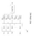
- FIG. 1illustrates a conventional memory system.
- system 100includes charge pump 102 , switches 104 - 112 , and memory blocks 114 - 120 .
- components 102 - 120are formed on the surface of a substrate.
- Charge pump 102is a conventional circuit implementation used to step up a voltage which is passed through one of switches 104 - 112 in order to select an element (not shown) in one of memory blocks 114 - 120 .
- Voltages from charge pump 102are large and used for programmable sequences in memory blocks 114 - 120 . However, large voltages generated by charge pump 102 can create disturbances or “disturb effects” in surrounding elements other than those desired.
- a disturb effectresults from the generation of a large voltage by charge pump 102 , which changes the resistive state or inadvertently programs or erases a non-selected element.
- Conventional memory systemssuffer from large charge pump sizes and outputs, which require large die sizes, create error and disturb effects, and increase fabrication and operational expenses.
- FIG. 1illustrates a conventional memory system
- FIG. 2Aillustrates an exemplary memory power management system
- FIG. 2Billustrates an alternative exemplary memory power management system
- FIG. 3illustrates an exemplary memory control system suitable for memory power management
- FIG. 4Aillustrates an exemplary memory system configuration suitable for memory power management
- FIG. 4Bis an alternative view of an exemplary memory system configuration suitable for memory power management
- FIG. 4Cis an exemplary die configuration suitable for memory power management
- FIG. 5is a cross-sectional view of an exemplary memory system suitable for memory power management
- FIG. 6is a flow chart illustrating an exemplary method for managing power
- FIG. 7is a block diagram illustrating an exemplary computer system suitable for memory power management.
- the inventioncan be implemented in numerous ways, including as a system, a process, an apparatus, or a series of program instructions on a computer readable medium such as a computer readable storage medium or a computer network where the program instructions are sent over optical or electronic communication links.
- a computer readable mediumsuch as a computer readable storage medium or a computer network where the program instructions are sent over optical or electronic communication links.
- the steps of disclosed processesmay be performed in an arbitrary order, unless otherwise provided in the claims.
- Memory systemsmay be implemented using non-volatile third dimension memory arrays coupled to logic and charge pump circuitry to reduce die size, allow for reduced power requirements, and increased accesses for programmable sequences.
- a memoryis “third dimension memory” when it is fabricated above other circuitry components, the components usually including a silicon substrate, polysilicon layers and, typically, metallization layers.
- memory systemsmay be vertically-configured to reduce die size and not sacrifice overall chip functionality.
- the applicationdescribes a two terminal memory element that changes conductivity when exposed to an appropriate voltage drop across the two terminals.
- the memory elementincludes an electrolytic tunnel barrier and a mixed valence conductive oxide. A voltage drop across the electrolytic tunnel barrier causes an electrical field within the mixed valence conductive oxide that is strong enough to move oxygen ions out of the mixed valence conductive oxide and into the electrolytic tunnel barrier.
- Oxygen depletioncauses the mixed valence conductive oxide to change its valence, which causes a change in conductivity.
- Both the electrolytic tunnel barrier and the mixed valence conductive oxidedo not need to operate in a silicon substrate, and, therefore, can be fabricated above circuitry being used for other purposes (such as selection circuitry).
- two-terminal memory elementscan be arranged in a cross point array such that one terminal is electrically coupled with an x-direction line and the other terminal is electrically coupled with a y-direction line.
- a stacked cross point arrayconsists of multiple cross point arrays stacked upon one another, sometimes sharing x-direction and y-direction lines between layers, and sometimes having isolated lines. Both single-layer cross point arrays and stacked cross point arrays may be arranged as third dimension memories.
- Memory arraysmay be implemented using layers of memory elements that may be used in blocks or sub-blocks to store data.
- driving voltage requirementsmay be met by using multiple, smaller charge pumps.
- multiple, simultaneous accesses of memory elements in a memory arraymay be performed. While various types and designs of charge pump circuits may be used, the implementation of multiple, smaller charge pumps in a third dimension memory allows for die size to be reduced while improving chip capabilities, including faster access times for performing multiple, simultaneous programmable sequences.
- FIG. 2Aillustrates an exemplary memory power management system.
- system 200includes charge pumps 202 - 204 , physical partitions 206 - 236 , and switches 240 - 247 .
- switches 240 - 247are grouped in pairs, each member of a pair of switches gating voltages to a partition based on either an X or Y coordinate.
- a programmable sequencemay be performed at a desired location in a memory array, whether in a block, sub-block, plane, sub-plane, or any other type of partition.
- X and Y coordinate switches 242 and 243gate driving voltages from charge pumps 202 - 204 to one or more locations within physical partitions 216 and 208 , which lie on sub-planes 2 and 3 of sub-block 1 of the memory array.
- physical partitions 206 - 236represent a plurality of conductive array lines.
- Memory elements(not shown) are located at the intersection of conductive array lines in adjacent sub-planes.
- physical partitions 216 and 208selectively address memory elements at the intersections of activated conductive array lines within the physical partitions 216 and 208 .
- Charge pumps 202 - 204generate voltages that are used to perform programmable sequences on memory elements electrically connected to physical partitions 206 - 236 .
- physical partitions 206 - 236may be grouped together in sub-planes (e.g., sub-planes 0 , 1 , 2 , 3 , and the like) and sub-blocks (e.g., memory sub-blocks 0 , 1 , 2 , 3 , and the like). Different sub-blocks may be grouped together as blocks of a memory array. Adjacent sub-planes and the memory elements between them constitute a memory plane (“plane” or “memory layer”).
- memory elementsare located between every sub-plane such that a physical partition may drive two sub-planes of memory (e.g., one plane includes sub-planes 0 and 1 , another plane includes sub-planes 1 and 2 , another plane includes sub-planes 2 and 3 , and the like).
- physical partitionsmay drive a single sub-plane of memory (e.g., one plane includes sub-planes 0 and 1 and another plane includes sub-planes 2 and 3 ).
- Individual memory elements (not shown) between adjacent physical partitionsstore data values, which may be read or written by applying a voltage generated by charge pumps 202 - 204 .
- the number, type, configuration, and properties of partitions, sub-blocks, and planesmay be varied and are not limited to the example shown.
- charge pumps 202 - 204generate voltages that are switched through switches 240 - 247 to memory elements between physical partitions 206 - 236 .
- the voltagechanges the resistive state of the element to store a data value, which may be indicative of a “0” or “1” or other values if intermediary resistive states are used (e.g., indicative of “00,” “01,” “10” or “11”).
- “Writing”is the process of changing the resistive state (measured at the read voltage), regardless of whether the change is from a high resistance to a low resistance or a low resistance to a high resistance. Power is driven to system 200 using voltages generated by charge pumps 202 - 204 and applied to physical partitions 206 - 236 .
- voltagesWhen applied, voltages change the conductivity profile of a memory element, which may be implemented as stacks of material deposited at the intersection of a row and column electrodes (not shown), thus enabling a binary value to be read or written.
- Logic(not shown) coupled to charge pumps 202 - 204 directs the application of voltages to elements in physical partitions 206 - 236 .
- Switches 240 - 247may be activated in order to direct a voltage to a desired partition to read or write data.
- operationssuch as reads and writes may be performed simultaneously without using charge pump circuitry designed for the output of large voltages.
- voltagesmay be generated and independently “gated” (i.e., routed or switched to a particular element) through switches 240 - 247 to physical partitions 206 - 236 .
- Charge pump B 204provides a positive driving voltage to switches 240 , 242 , 244 and 246 , which gate driving voltages to the desired elements based on the appropriate X and Y coordinates.
- Charge pump A 202provides negative driving voltages through switches 241 , 243 , 245 and 247 , which gate driving voltages to the desired elements based on the appropriate X and Y coordinates.
- charge pump A 202 and charge pump B 204simultaneously output voltages of opposite polarities, the total voltage drop across the memory element can be higher than the output of either charge pump 202 and 204 .
- the total voltage drop across the memory elementwould need to be one polarity to write in one direction (e.g., from low resistance to high resistance) and an opposite polarity to write in the opposite direction (e.g., from high resistance to low resistance).
- switch 242would apply the output of charge pump B 204 to physical partition 208 while switch 243 would apply the output of charge pump A 202 to physical partition 216 .
- switch 243would apply the output of charge pump A 202 to physical partition 208 while switch 242 would apply the output of charge pump B 204 to physical partition 216 .
- the use of multiple charge pumps that are independently gatedallows multiple simultaneous operations to be performed on memory elements in different sub-blocks. Further, by using multiple charge pumps with a third dimension memory array, simultaneous reads and writes may be performed without increasing die size.
- Other components, input and output voltages, and circuit and component descriptionsmay be used and are not limited to those described above.
- FIG. 2Billustrates an alternative exemplary memory power management system. Similar to system 200 described above in connection with FIG. 2A , system 250 includes charge pumps 202 - 204 and physical partitions 206 - 236 . However, each physical partition 206 - 236 has a dedicated pair of switches 255 - 286 , instead of the design illustrated in FIG. 2A in which each sub-block had a dedicated pair of switches 240 - 247 . In other words, the “logical partitions” that can be independently controlled are sub-blocks in FIG. 2A and physical partitions in FIG. 2B . Each switch in a pair gates voltages to a partition based on X and Y coordinates.
- an element disposed at the intersection of two conductive array linesmay be located within an array, whether in a block, sub-block, or any other type of partition.
- switches 273 - 274are used to gate driving voltages from charge pumps 202 - 204 to one or more locations within physical partition 216 , which lies in sub-plane 2 and sub-block 1 of the memory array.
- Switches 255 - 286gate voltages based on an X and Y coordinate pair assigned to each location within physical partitions 206 - 236 .
- sub-blocks, sub-planes, partitions, and memory elementsmay be located and accessed to perform operations.
- Logic(not shown) coupled to system 250 determines which memory element is being requested for access to perform a desired read or write operation or other programmable sequence. Based upon that determination, charge pumps 202 - 204 are directed to generate driving voltages that are sent to a memory element or group of memory elements electrically connected to physical partitions 206 - 236 . For example, if a memory element between physical partitions 208 and 216 needed to write a “1”, switch 281 would apply the output of charge pump B 204 to physical partition 208 while switch 274 would apply the output of charge pump A 202 to physical partition 216 .
- Switches 273 and 282would be turned off. However, if the same memory element needed to write a “0”, then switches 281 and 274 would be turned off while switch 282 would apply the output of charge pump A 202 to physical partition 208 while switch 273 would apply the output of charge pump B 204 to physical partition 216 .
- FIG. 2A and FIG. 2Bmultiple charge pumps that are independently gated allow more than one programmable sequence to be performed simultaneously. However, it should be appreciated that it may not be desirable to execute a programming sequence on all available partitions. For example, in FIG. 2A , if only the memory elements in sub-blocks 1 and 2 needed to be modified, then only switches 242 - 245 would be active.
- FIG. 3illustrates an exemplary memory control system suitable for memory power management.
- System 300enables data to be stored and retrieved from various memory locations and may be used to provide control logic with memory systems such as those described above in connection with FIGS. 2A-2B .
- system 300includes processor 302 , memory (e.g., read only memory or ROM) 304 , memory (e.g., random access memory or RAM) 306 , memory controller 308 , host interface (I/F) block 310 , direct memory access (DMA) block 312 , memory 314 , buffer memory 316 , error correction code (which may also be referred to as error checking and correction or ECC) 318 , defect management block 320 , interface driver/receiver 322 , and interface (I/F) state machine (SM) 324 .
- processor 302e.g., memory (e.g., read only memory or ROM) 304 , memory (e.g., random access memory or RAM) 306 , memory controller
- Memory implementations in system 300may be implemented as RAM, ROM, dynamic random access memory (DRAM), static/dynamic random access memory (SDRAM), and others.
- Buffer memory 316may be implemented to temporarily store and access data while system 300 is operating (i.e., receiving power) enabling faster data processing.
- buffer memory 316may be implemented as a first-in, first-out (FIFO) buffer.
- FIFOfirst-in, first-out
- buffer memory 316may be implemented differently. Other components are described, including logic for controlling operations that access memory locations throughout system 300 .
- the various modules included in system 300may be used to implement functionality for a storage system that interfaces with memory systems and other external systems that either request or store data in system 300 .
- External systemsmay include other software or hardware that, through I/F Drv/Rec 322 , interfaces with system 300 to retrieve or store data.
- more or fewer modulesmay be included in system 300 .
- different modulesmay be used to implement various types of functionality beyond that described above.
- processor 302provides logic configured to provide controller functions.
- Software code written in languages such as Cmay provide instruction sets on how system 300 processes requests to either retrieve or store data from various memory locations in system 300 .
- Other functions performed by processor 302may include initializing controller logic when power is applied (i.e., “on” voltage is applied), performing diagnostic checks, interpreting commands for memory functions, memory management, ECC-related functions, and others.
- Processor 302also interprets commands from host I/F 310 to establish data flow control using DMA 312 .
- Host I/F 310may be used to implement complex functionality that enables system 300 to integrate with other systems, for example, in a computer.
- host I/F 310Some functions that may be performed by host I/F 310 include encoding/decoding (e.g., 8-bit/10-bit), scrambling (to reduce electromagnetic interference (EMI)), parity/cyclic redundancy check (CRC)/ECC checking, disparity generation and checking, interface state machine functions, data buffer (e.g., first-in, first-out (FIFO)), alignment and primitive check and generation (e.g., checks performed on serial interfaces), and others. Some of these functions may also be implemented using other modules with system 300 .
- encoding/decodinge.g., 8-bit/10-bit
- scramblingto reduce electromagnetic interference (EMI)
- CRCparity/cyclic redundancy check
- ECC checkingparity/cyclic redundancy check
- disparity generation and checkinginterface state machine functions
- data buffere.g., first-in, first-out (FIFO)
- FIFOfirst-in, first-out
- alignment and primitive check and generatione.g.
- system 300may be implemented as a memory card, including memory storage and controller logic.
- a memory cardmay be connected to host I/F 310 using an interface connector (not shown).
- a chip using system 300may be configured to receive electrical signals from external devices through an interface connector. The electrical signals are interpreted and acted upon depending upon an interface standard (e.g., IEEE) used for command and data passing. Electrical signals may be sent and received to pass data to and from memory 306 via host I/F 310 and memory controller 308 .
- Host I/F 310sends commands and data to memory 306 via DMA 312 and memory controller 308 .
- memory controller 308may be implemented as a DRAM controller, which may be used to access, retrieve, and store data in memory 306 while power is being supplied.
- Memory controller 308also determines addresses for data stored in memory 306 . Addresses may be referenced, for example, based on a row and column reference for a particular memory element in a given memory array. By selectively applying voltages to terminals connected to row and column leads, the resistive states of memory elements may be changed. The resistive states of memory elements may be changed to store binary data bits (e.g., whether a memory element's resistive state indicates a “0” or “1”). This “memory effect” applies to the various memory configurations described. In some examples, modules within system 300 may be third dimension memory. For example, memory 304 or memory 306 or other memory locations may be implemented as non-volatile third dimension memory.
- system 300may use multiple memory controllers to enable faster data retrieval and storage from various memory locations.
- DRAM technologymay be used to implement memory 306 and memory controller 308 .
- DRAMuses a “pulse” or “refresh” voltage to retain data in memory while power is on.
- Memory controller 308may be implemented using logic that processes data stored in and retrieved from memory 306 .
- multiple DRAM-based memory controllersmay be used in order to increase processing times.
- multiple DRAM layersmay be used to increase storage capacity.
- System 300may also include logic that determines how data is shared with external devices.
- I/F SM 324may be configured to send or receive data from an external device indicated by addresses in electrical signals.
- a “handshake”may be performed with the indicated external device through I/F Dev/Rec module 322 , which acts as a memory interface bus to establish a connection. After establishing a connection between the device and system 300 (via I/F Drv/Rec module 322 ), data may be passed between memory 304 , 306 , or 314 (via buffer memory 316 ) to the indicated device.
- I/F Dev/Rec module 322works in conjunction with I/F SM 324 , which performs handshaking and data flow handling to external devices using data in memory 304 or 306 controlled by system 300 .
- I/F SM 324may also include other functionality to support interfaces between system 300 and external devices. Devices may also include other processes, logic, circuits, components, or functionality included in an IC.
- FIG. 4Aillustrates an exemplary memory system configuration suitable for implementing memory power management.
- memory systemsmay be developed using third dimension memory.
- system 400is an example of a vertical configuration of layers 402 - 408 .
- Each layermay be divided into n sub-planes.
- functionality in a third dimension memorymay be tailored by using layers for different purposes while using a small die size.
- Metal or other materialsmay be used as conductive conduits that enable electrical current to flow between the memory array layers as “vias” or “thrus.” For example, vias, thrus and conductive array lines may be used to retrieve data from a particular memory element in a memory array implemented at layer 402 .
- Controller logic implemented at layer 408retrieves data stored at the memory array layer by sending an electrical current to determine the resistive state of the memory element (e.g., one resistive state may be interpreted as a “0” and another resistive state may be interpreted as a “1”).
- FIG. 4Bis an alternative view of an exemplary memory system configuration suitable for memory power management.
- system 410includes controller 412 , which is vertically configured with n memory array layers 414 - 422 .
- the number of memory array layers 414 - 422may be modified to include more or fewer layers than those shown. Additional functionality may also be implemented by controller 412 , as described above.
- memory array layers 414 - 422may be stacked in different numbers of layers to allow different circuit patterns of varying configurations to be implemented (i.e., printed) using a single mask set during fabrication.
- circuitrymay be varied. For example, if a circuit having a small memory controller capacity is desired, a single memory layer may be implemented in a vertical stack during the fabrication process. If more capacity is desired, multiple memory array layers may be added until design and process constraints are reached. For example, although three (3) memory array layers are shown in system 400 , any number of layers may be used.
- FIG. 4Cis an exemplary die configuration suitable for memory power management.
- Substrate 422includes memory array 432 , controller 434 , and charge pumps 436 - 438 . Included on substrate 422 are various circuitry modules (e.g., memory array 432 , controller 434 , charge pumps 436 - 438 , and the like) that may be printed or fabricated on, with, or integrated into substrate 422 .
- an alternative die configurationmay be used to illustrate the various types of components or circuitry that may be implemented onto a substrate.
- circuitrymay be integrated with memory array 432 in a vertically-stacked configuration, providing a physically-reduced memory system footprint on substrate 422 .
- various types and configurations of circuitrymay be used and are not limited to the configuration shown with substrate 422 .
- FIG. 5Ais cross-sectional view of an exemplary memory system using memory power management.
- system 500includes column electrodes 502 - 540 , row electrodes 542 - 548 , charge pump (X coordinate) 552 , charge pump (Y coordinate) 554 , and controller 550 .
- column electrodes 502 - 540 and row electrodes 542 - 548are conductive array lines that are coupled by either direct or indirect connections (not shown) to each sub-plane of a memory array.
- Column electrodes 502 - 540 , row electrodes 542 - 548 , connections between both types of electrodes, and memory materials used for memory elementsmay be implemented using various types of conductive or semi-conductive materials and are not limited to any particular type.
- Column electrodes 502 - 510are configured on sub-plane 0
- column electrodes 512 - 520are configured on sub-plane 2
- column electrodes 522 - 530are configured on sub-plane 4
- column electrodes 532 - 540are configured on sub-plane 6 .
- row electrodes 542 - 548are configured on odd-numbered sub-planes (e.g., 1 , 3 , 5 , and the like).
- Other row electrodesmay be disposed relative to row electrodes 542 - 548 and lying orthogonal to column electrodes 502 - 540 .
- intersections of row electrodes 542 - 548 and column electrodes 502 - 540create a memory array and each intersection represents an element configured to store a data value (e.g., “0,” “1”). In other examples, different configurations may be implemented other than those shown.
- charge pump (X coordinate) 552 and charge pump (Y coordinate) 554are coupled to column electrodes 502 - 540 and row electrodes 542 - 548 , respectively.
- charge pump (X coordinate) 552 and charge pump (Y coordinate) 554may be implemented differently, including using different circuit patterns, conductive materials, varying the number of layers used in system 500 .
- FIG. 6is a flow chart illustrating an exemplary method for managing power.
- a driving voltageis generated by a pair of charge pumps in a memory system such as those described above ( 602 ). Once generated, the driving voltage is gated to a memory element in a memory array included in the memory system ( 604 ). The driving voltage may be independently gated or otherwise routed from the charge pumps to a desired memory element in the memory array. After gating the driving voltage to the desired element, an access and operation (e.g., read or write) is performed ( 606 ).
- multiple charge pumpsmay be used to perform simultaneous accesses.
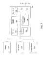
- FIG. 7is a block diagram illustrating an exemplary computer system suitable for memory power management.
- computer system 700may be used to implement computer programs, applications, methods, or other software to perform the above-described techniques.
- Computer system 700includes a bus 702 or other communication mechanism for communicating information, which interconnects subsystems and devices, such as processor 704 , system memory 706 (e.g., RAM), storage device 708 (e.g., ROM), disk drive 710 (e.g., magnetic or optical), communication interface 712 (e.g., modem or Ethernet card), display 714 (e.g., CRT or LCD), input device 716 (e.g., keyboard), and cursor control 718 (e.g., mouse or trackball).
- processor 704e.g., system memory 706 (e.g., RAM), storage device 708 (e.g., ROM), disk drive 710 (e.g., magnetic or optical), communication interface 712 (e.g., modem or Ethernet card), display 714 (
- computer system 700performs specific operations by processor 704 executing one or more sequences of one or more instructions stored in system memory 706 .
- Such instructionsmay be read into system memory 706 from another computer readable medium, such as static storage device 708 or disk drive 710 .
- static storage device 708 or disk drive 710may be used in place of or in combination with software instructions to implement the invention.
- Non-volatile mediaincludes, for example, optical or magnetic disks, such as disk drive 710 .
- Volatile mediaincludes dynamic memory, such as system memory 706 .
- Transmission mediaincludes coaxial cables, copper wire, and fiber optics, including wires that comprise bus 702 . Transmission media can also take the form of acoustic or light waves, such as those generated during radio wave and infrared data communications.
- Computer readable mediaincludes, for example, floppy disk, flexible disk, hard disk, magnetic tape, any other magnetic medium, CD-ROM, any other optical medium, punch cards, paper tape, any other physical medium with patterns of holes, RAM, PROM, EPROM, FLASH-EPROM, any other memory chip or cartridge, carrier wave, or any other medium from which a computer can read.
- Computer system 700may transmit and receive messages, data, and instructions, including program, i.e., application code, through communication link 720 and communication interface 712 .
- Received program codemay be executed by processor 704 as it is received, and/or stored in disk drive 710 , or other non-volatile storage for later execution.
Landscapes
- Engineering & Computer Science (AREA)
- Power Engineering (AREA)
- Semiconductor Memories (AREA)
- Read Only Memory (AREA)
Abstract
Description
- The present invention relates generally to semiconductors and memory technology. More specifically, memory power management is described.
- Conventional memory systems (e.g., storage systems, disk drives, hard disks, memory chips, memory devices, and the like) are fabricated using technologies such as static random access memory (SRAM), dynamic random access memory (DRAM), or non-volatile implementations (e.g., Flash). However, conventional memory systems are problematic because of the need to increase functionality while reducing die sizes.
- Memory controllers, logic circuitry, or other components in conventional implementations often require large die sizes in order to accommodate various components or circuits. Conventional implementations often use components such as multiple processors, buffer memory, error correction code (ECC), and direct memory access (DMA) circuits for fast movement of data. Demands for increasingly complex, faster, and larger memory arrays require chips with greater functionality, but smaller die sizes. However, conventional implementations use large circuit patterns that require large die sizes. Due to conventional circuit patterns and component design, power requirements and heat generation are high, which lead to memory system failures and errors. Another issue with conventional implementations is the amount of driving voltage required to program and erase memory cells or elements (“elements”) in conventional memory arrays.
- In conventional implementations, driving voltages are generated by circuits known as charge pumps. Charge pumps may be used to receive an input voltage, transfer power using one or more capacitors, and generate an output or driving voltage that is larger or smaller than the input voltage. An output voltage is stabilized and “driven” to a desired voltage level in order to cause a program operation (e.g., read, write, and erase) to occur in elements of a memory array. The voltages generated by conventional charge pumps are limited by factors such as the amount of available current, the size of capacitors used in a charge pump circuit, and the quantity of charge pumps used to generate voltages for the programmable sequences. In conventional memory systems, charge pumps are often implemented using circuitry that can generate large output voltages, thus requiring more or larger capacitors, which are used to store and transfer voltages required to perform a programmable sequence (e.g., read, write, erase). Capacitors in conventional charge pump circuits are designed to support large voltages or stepped up voltages, which requires large die sizes. Further, as conventional memory arrays increase in capacity, the size of conventional charge pumps and the required amount of driving voltages also increase. Combined with conventional charge pumps, conventional memory systems are difficult and expensive to manufacture and operate.
FIG. 1 illustrates a conventional memory system. In conventional implementations,system 100 includescharge pump 102, switches104-112, and memory blocks114-120. Here, a functional perspective is shown and in conventional implementations, components102-120 are formed on the surface of a substrate.Charge pump 102 is a conventional circuit implementation used to step up a voltage which is passed through one of switches104-112 in order to select an element (not shown) in one of memory blocks114-120. Voltages fromcharge pump 102 are large and used for programmable sequences in memory blocks114-120. However, large voltages generated bycharge pump 102 can create disturbances or “disturb effects” in surrounding elements other than those desired. A disturb effect results from the generation of a large voltage bycharge pump 102, which changes the resistive state or inadvertently programs or erases a non-selected element. Conventional memory systems suffer from large charge pump sizes and outputs, which require large die sizes, create error and disturb effects, and increase fabrication and operational expenses.- Continuing efforts are being made to improve memory systems.
- Various embodiments of the invention are disclosed in the following detailed description and the accompanying drawings:
FIG. 1 illustrates a conventional memory system;FIG. 2A illustrates an exemplary memory power management system;FIG. 2B illustrates an alternative exemplary memory power management system;FIG. 3 illustrates an exemplary memory control system suitable for memory power management;FIG. 4A illustrates an exemplary memory system configuration suitable for memory power management;FIG. 4B is an alternative view of an exemplary memory system configuration suitable for memory power management;FIG. 4C is an exemplary die configuration suitable for memory power management;FIG. 5 is a cross-sectional view of an exemplary memory system suitable for memory power management;FIG. 6 is a flow chart illustrating an exemplary method for managing power; andFIG. 7 is a block diagram illustrating an exemplary computer system suitable for memory power management.- It is to be understood that the depictions in the FIGs are not necessarily to scale. Although various examples of the invention are disclosed in the accompanying drawings, the invention is not limited to those specific examples.
- The invention can be implemented in numerous ways, including as a system, a process, an apparatus, or a series of program instructions on a computer readable medium such as a computer readable storage medium or a computer network where the program instructions are sent over optical or electronic communication links. In general, the steps of disclosed processes may be performed in an arbitrary order, unless otherwise provided in the claims.
- A detailed description of one or more embodiments is provided below along with accompanying figures. The detailed description is provided in connection with such embodiments, but is not limited to any particular example. The scope is limited only by the claims, and numerous alternatives, modifications, and equivalents are encompassed. Numerous specific details are set forth in the following description in order to provide a thorough understanding. These details are provided for the purpose of example and the described techniques may be practiced according to the claims without some or all of these specific details. For the purpose of clarity, technical material that is known in the technical fields related to the embodiments has not been described in detail to avoid unnecessarily obscuring the description.
- Memory systems may be implemented using non-volatile third dimension memory arrays coupled to logic and charge pump circuitry to reduce die size, allow for reduced power requirements, and increased accesses for programmable sequences. A memory is “third dimension memory” when it is fabricated above other circuitry components, the components usually including a silicon substrate, polysilicon layers and, typically, metallization layers. By using non-volatile third dimension memory arrays, memory systems may be vertically-configured to reduce die size and not sacrifice overall chip functionality.
- U.S. patent application Ser. No. 11/095,026, filed Mar. 30, 2005, and titled “Memory Using Mixed Valence Conductive Oxides,” hereby incorporated by reference in its entirety and for all purposes, describes non-volatile third dimension memory cells that can be arranged in a cross point array. The application describes a two terminal memory element that changes conductivity when exposed to an appropriate voltage drop across the two terminals. The memory element includes an electrolytic tunnel barrier and a mixed valence conductive oxide. A voltage drop across the electrolytic tunnel barrier causes an electrical field within the mixed valence conductive oxide that is strong enough to move oxygen ions out of the mixed valence conductive oxide and into the electrolytic tunnel barrier. Oxygen depletion causes the mixed valence conductive oxide to change its valence, which causes a change in conductivity. Both the electrolytic tunnel barrier and the mixed valence conductive oxide do not need to operate in a silicon substrate, and, therefore, can be fabricated above circuitry being used for other purposes (such as selection circuitry). Additionally, two-terminal memory elements can be arranged in a cross point array such that one terminal is electrically coupled with an x-direction line and the other terminal is electrically coupled with a y-direction line. A stacked cross point array consists of multiple cross point arrays stacked upon one another, sometimes sharing x-direction and y-direction lines between layers, and sometimes having isolated lines. Both single-layer cross point arrays and stacked cross point arrays may be arranged as third dimension memories.
- Memory arrays may be implemented using layers of memory elements that may be used in blocks or sub-blocks to store data. By utilizing third dimension memory, driving voltage requirements may be met by using multiple, smaller charge pumps. Further, multiple, simultaneous accesses of memory elements in a memory array may be performed. While various types and designs of charge pump circuits may be used, the implementation of multiple, smaller charge pumps in a third dimension memory allows for die size to be reduced while improving chip capabilities, including faster access times for performing multiple, simultaneous programmable sequences.
FIG. 2A illustrates an exemplary memory power management system. Here,system 200 includes charge pumps202-204, physical partitions206-236, and switches240-247. In some examples, switches240-247 are grouped in pairs, each member of a pair of switches gating voltages to a partition based on either an X or Y coordinate. By referencing a memory element using X and Y coordinates, a programmable sequence may be performed at a desired location in a memory array, whether in a block, sub-block, plane, sub-plane, or any other type of partition. For example, X and Y coordinateswitches physical partitions sub-planes sub-block 1 of the memory array. In this example, physical partitions206-236 represent a plurality of conductive array lines. Memory elements (not shown) are located at the intersection of conductive array lines in adjacent sub-planes. Togetherphysical partitions physical partitions memory sub-blocks - Here, charge pumps202-204 generate voltages that are switched through switches240-247 to memory elements between physical partitions206-236. When applied, the voltage changes the resistive state of the element to store a data value, which may be indicative of a “0” or “1” or other values if intermediary resistive states are used (e.g., indicative of “00,” “01,” “10” or “11”). “Writing” is the process of changing the resistive state (measured at the read voltage), regardless of whether the change is from a high resistance to a low resistance or a low resistance to a high resistance. Power is driven to
system 200 using voltages generated by charge pumps202-204 and applied to physical partitions206-236. When applied, voltages change the conductivity profile of a memory element, which may be implemented as stacks of material deposited at the intersection of a row and column electrodes (not shown), thus enabling a binary value to be read or written. Logic (not shown) coupled to charge pumps202-204 directs the application of voltages to elements in physical partitions206-236. Switches240-247 may be activated in order to direct a voltage to a desired partition to read or write data. By using charge pumps202-204 and a memory array having physical partitions206-236, operations such as reads and writes may be performed simultaneously without using charge pump circuitry designed for the output of large voltages. In some examples, voltages may be generated and independently “gated” (i.e., routed or switched to a particular element) through switches240-247 to physical partitions206-236. Charge pump B 204 provides a positive driving voltage toswitches Charge pump A 202 provides negative driving voltages throughswitches charge pump A 202 andcharge pump B 204 simultaneously output voltages of opposite polarities, the total voltage drop across the memory element can be higher than the output of eithercharge pump physical partitions switch 242 would apply the output ofcharge pump B 204 tophysical partition 208 whileswitch 243 would apply the output ofcharge pump A 202 tophysical partition 216. However, if the same memory element needed to write the equivalent of a “0” value over an existing “1”, then switch243 would apply the output ofcharge pump A 202 tophysical partition 208 whileswitch 242 would apply the output ofcharge pump B 204 tophysical partition 216. The use of multiple charge pumps that are independently gated allows multiple simultaneous operations to be performed on memory elements in different sub-blocks. Further, by using multiple charge pumps with a third dimension memory array, simultaneous reads and writes may be performed without increasing die size. Other components, input and output voltages, and circuit and component descriptions may be used and are not limited to those described above.FIG. 2B illustrates an alternative exemplary memory power management system. Similar tosystem 200 described above in connection withFIG. 2A ,system 250 includes charge pumps202-204 and physical partitions206-236. However, each physical partition206-236 has a dedicated pair of switches255-286, instead of the design illustrated inFIG. 2A in which each sub-block had a dedicated pair of switches240-247. In other words, the “logical partitions” that can be independently controlled are sub-blocks inFIG. 2A and physical partitions inFIG. 2B . Each switch in a pair gates voltages to a partition based on X and Y coordinates. By using X and Y coordinates, an element disposed at the intersection of two conductive array lines (e.g., the intersection of a pair of row and column electrodes) may be located within an array, whether in a block, sub-block, or any other type of partition. For example, switches273-274 are used to gate driving voltages from charge pumps202-204 to one or more locations withinphysical partition 216, which lies insub-plane 2 andsub-block 1 of the memory array. Switches255-286 gate voltages based on an X and Y coordinate pair assigned to each location within physical partitions206-236. By using X and Y coordinates, sub-blocks, sub-planes, partitions, and memory elements, may be located and accessed to perform operations. Logic (not shown) coupled tosystem 250 determines which memory element is being requested for access to perform a desired read or write operation or other programmable sequence. Based upon that determination, charge pumps202-204 are directed to generate driving voltages that are sent to a memory element or group of memory elements electrically connected to physical partitions206-236. For example, if a memory element betweenphysical partitions switch 281 would apply the output ofcharge pump B 204 tophysical partition 208 whileswitch 274 would apply the output ofcharge pump A 202 tophysical partition 216.Switches switch 282 would apply the output ofcharge pump A 202 tophysical partition 208 whileswitch 273 would apply the output ofcharge pump B 204 tophysical partition 216.- In both
FIG. 2A andFIG. 2B multiple charge pumps that are independently gated allow more than one programmable sequence to be performed simultaneously. However, it should be appreciated that it may not be desirable to execute a programming sequence on all available partitions. For example, inFIG. 2A , if only the memory elements insub-blocks FIG. 3 illustrates an exemplary memory control system suitable for memory power management.System 300 enables data to be stored and retrieved from various memory locations and may be used to provide control logic with memory systems such as those described above in connection withFIGS. 2A-2B . Here,system 300 includesprocessor 302, memory (e.g., read only memory or ROM)304, memory (e.g., random access memory or RAM)306,memory controller 308, host interface (I/F) block310, direct memory access (DMA) block312,memory 314,buffer memory 316, error correction code (which may also be referred to as error checking and correction or ECC)318,defect management block 320, interface driver/receiver 322, and interface (I/F) state machine (SM)324. Memory implementations insystem 300 may be implemented as RAM, ROM, dynamic random access memory (DRAM), static/dynamic random access memory (SDRAM), and others.Buffer memory 316 may be implemented to temporarily store and access data whilesystem 300 is operating (i.e., receiving power) enabling faster data processing. In some examples,buffer memory 316 may be implemented as a first-in, first-out (FIFO) buffer. In other examples,buffer memory 316 may be implemented differently. Other components are described, including logic for controlling operations that access memory locations throughoutsystem 300.- The various modules included in
system 300 may be used to implement functionality for a storage system that interfaces with memory systems and other external systems that either request or store data insystem 300. External systems may include other software or hardware that, through I/F Drv/Rec 322, interfaces withsystem 300 to retrieve or store data. In other examples, more or fewer modules may be included insystem 300. Further, different modules may be used to implement various types of functionality beyond that described above. - Here,
processor 302 provides logic configured to provide controller functions. Software code written in languages such as C may provide instruction sets on howsystem 300 processes requests to either retrieve or store data from various memory locations insystem 300. Other functions performed byprocessor 302 may include initializing controller logic when power is applied (i.e., “on” voltage is applied), performing diagnostic checks, interpreting commands for memory functions, memory management, ECC-related functions, and others.Processor 302 also interprets commands from host I/F 310 to establish data flowcontrol using DMA 312. Host I/F 310 may be used to implement complex functionality that enablessystem 300 to integrate with other systems, for example, in a computer. Some functions that may be performed by host I/F 310 include encoding/decoding (e.g., 8-bit/10-bit), scrambling (to reduce electromagnetic interference (EMI)), parity/cyclic redundancy check (CRC)/ECC checking, disparity generation and checking, interface state machine functions, data buffer (e.g., first-in, first-out (FIFO)), alignment and primitive check and generation (e.g., checks performed on serial interfaces), and others. Some of these functions may also be implemented using other modules withsystem 300. - In some examples,
system 300 may be implemented as a memory card, including memory storage and controller logic. A memory card may be connected to host I/F 310 using an interface connector (not shown). Achip using system 300 may be configured to receive electrical signals from external devices through an interface connector. The electrical signals are interpreted and acted upon depending upon an interface standard (e.g., IEEE) used for command and data passing. Electrical signals may be sent and received to pass data to and frommemory 306 via host I/F 310 andmemory controller 308. Host I/F 310 sends commands and data tomemory 306 viaDMA 312 andmemory controller 308. In some examples,memory controller 308 may be implemented as a DRAM controller, which may be used to access, retrieve, and store data inmemory 306 while power is being supplied.Memory controller 308 also determines addresses for data stored inmemory 306. Addresses may be referenced, for example, based on a row and column reference for a particular memory element in a given memory array. By selectively applying voltages to terminals connected to row and column leads, the resistive states of memory elements may be changed. The resistive states of memory elements may be changed to store binary data bits (e.g., whether a memory element's resistive state indicates a “0” or “1”). This “memory effect” applies to the various memory configurations described. In some examples, modules withinsystem 300 may be third dimension memory. For example,memory 304 ormemory 306 or other memory locations may be implemented as non-volatile third dimension memory. - Here,
system 300 may use multiple memory controllers to enable faster data retrieval and storage from various memory locations. In some examples, DRAM technology may be used to implementmemory 306 andmemory controller 308. DRAM uses a “pulse” or “refresh” voltage to retain data in memory while power is on.Memory controller 308 may be implemented using logic that processes data stored in and retrieved frommemory 306. In some examples, multiple DRAM-based memory controllers may be used in order to increase processing times. In still other examples, multiple DRAM layers may be used to increase storage capacity.System 300 may also include logic that determines how data is shared with external devices. - In some examples, I/
F SM 324 may be configured to send or receive data from an external device indicated by addresses in electrical signals. A “handshake” may be performed with the indicated external device through I/F Dev/Rec module 322, which acts as a memory interface bus to establish a connection. After establishing a connection between the device and system300 (via I/F Drv/Rec module322), data may be passed betweenmemory Rec module 322 works in conjunction with I/F SM 324, which performs handshaking and data flow handling to external devices using data inmemory system 300. I/F SM 324 may also include other functionality to support interfaces betweensystem 300 and external devices. Devices may also include other processes, logic, circuits, components, or functionality included in an IC. FIG. 4A illustrates an exemplary memory system configuration suitable for implementing memory power management. In some examples, memory systems may be developed using third dimension memory. Here,system 400 is an example of a vertical configuration of layers402-408. Each layer may be divided into n sub-planes. By dividing each layer into sub-planes, functionality in a third dimension memory may be tailored by using layers for different purposes while using a small die size. Metal or other materials may be used as conductive conduits that enable electrical current to flow between the memory array layers as “vias” or “thrus.” For example, vias, thrus and conductive array lines may be used to retrieve data from a particular memory element in a memory array implemented atlayer 402. Controller logic implemented atlayer 408, based on an address (e.g., X and Y coordinates) for the desired memory element in the memory array, retrieves data stored at the memory array layer by sending an electrical current to determine the resistive state of the memory element (e.g., one resistive state may be interpreted as a “0” and another resistive state may be interpreted as a “1”).- Vertical configurations enable additional functionality without using large die sizes or incurring expensive testing methods and facilities for either combined controller/memory or separate controller and memory systems. Various types of functionality or circuitry may be used beyond those described above and are not limited to the examples shown.
FIG. 4B is an alternative view of an exemplary memory system configuration suitable for memory power management. In some examples,system 410 includescontroller 412, which is vertically configured with n memory array layers414-422. In other examples, the number of memory array layers414-422 may be modified to include more or fewer layers than those shown. Additional functionality may also be implemented bycontroller 412, as described above.- Here, memory array layers414-422 may be stacked in different numbers of layers to allow different circuit patterns of varying configurations to be implemented (i.e., printed) using a single mask set during fabrication. By increasing or decreasing the numbers of memory array layers, circuitry may be varied. For example, if a circuit having a small memory controller capacity is desired, a single memory layer may be implemented in a vertical stack during the fabrication process. If more capacity is desired, multiple memory array layers may be added until design and process constraints are reached. For example, although three (3) memory array layers are shown in
system 400, any number of layers may be used. FIG. 4C is an exemplary die configuration suitable for memory power management. Here, an alternative configuration of a memory system is shown.Substrate 422 includesmemory array 432,controller 434, and charge pumps436-438. Included onsubstrate 422 are various circuitry modules (e.g.,memory array 432,controller 434, charge pumps436-438, and the like) that may be printed or fabricated on, with, or integrated intosubstrate 422. In this example, an alternative die configuration may be used to illustrate the various types of components or circuitry that may be implemented onto a substrate. In some examples, circuitry may be integrated withmemory array 432 in a vertically-stacked configuration, providing a physically-reduced memory system footprint onsubstrate 422. However, various types and configurations of circuitry may be used and are not limited to the configuration shown withsubstrate 422.FIG. 5A is cross-sectional view of an exemplary memory system using memory power management. Here,system 500 includes column electrodes502-540, row electrodes542-548, charge pump (X coordinate)552, charge pump (Y coordinate)554, andcontroller 550. In some examples, column electrodes502-540 and row electrodes542-548 are conductive array lines that are coupled by either direct or indirect connections (not shown) to each sub-plane of a memory array. Column electrodes502-540, row electrodes542-548, connections between both types of electrodes, and memory materials used for memory elements may be implemented using various types of conductive or semi-conductive materials and are not limited to any particular type.- Column electrodes502-510 are configured on
sub-plane 0, column electrodes512-520 are configured onsub-plane 2, column electrodes522-530 are configured onsub-plane 4, and column electrodes532-540 are configured onsub-plane 6. Likewise, row electrodes542-548 are configured on odd-numbered sub-planes (e.g.,1,3,5, and the like). Other row electrodes may be disposed relative to row electrodes542-548 and lying orthogonal to column electrodes502-540. The intersections of row electrodes542-548 and column electrodes502-540 create a memory array and each intersection represents an element configured to store a data value (e.g., “0,” “1”). In other examples, different configurations may be implemented other than those shown. - Here, charge pump (X coordinate)552 and charge pump (Y coordinate)554 are coupled to column electrodes502-540 and row electrodes542-548, respectively. In other examples, charge pump (X coordinate)552 and charge pump (Y coordinate)554 may be implemented differently, including using different circuit patterns, conductive materials, varying the number of layers used in
system 500. FIG. 6 is a flow chart illustrating an exemplary method for managing power. In some examples, a driving voltage is generated by a pair of charge pumps in a memory system such as those described above (602). Once generated, the driving voltage is gated to a memory element in a memory array included in the memory system (604). The driving voltage may be independently gated or otherwise routed from the charge pumps to a desired memory element in the memory array. After gating the driving voltage to the desired element, an access and operation (e.g., read or write) is performed (606). Here, multiple charge pumps may be used to perform simultaneous accesses.FIG. 7 is a block diagram illustrating an exemplary computer system suitable for memory power management. In some examples,computer system 700 may be used to implement computer programs, applications, methods, or other software to perform the above-described techniques.Computer system 700 includes abus 702 or other communication mechanism for communicating information, which interconnects subsystems and devices, such asprocessor 704, system memory706 (e.g., RAM), storage device708 (e.g., ROM), disk drive710 (e.g., magnetic or optical), communication interface712 (e.g., modem or Ethernet card), display714 (e.g., CRT or LCD), input device716 (e.g., keyboard), and cursor control718 (e.g., mouse or trackball).- According to some examples of the invention,
computer system 700 performs specific operations byprocessor 704 executing one or more sequences of one or more instructions stored insystem memory 706. Such instructions may be read intosystem memory 706 from another computer readable medium, such asstatic storage device 708 ordisk drive 710. In some examples, hard-wired circuitry may be used in place of or in combination with software instructions to implement the invention. - The term “computer readable medium” refers to any medium that participates in providing instructions to
processor 704 for execution. Such a medium may take many forms, including but not limited to, non-volatile media, volatile media, and transmission media. Non-volatile media includes, for example, optical or magnetic disks, such asdisk drive 710. Volatile media includes dynamic memory, such assystem memory 706. Transmission media includes coaxial cables, copper wire, and fiber optics, including wires that comprisebus 702. Transmission media can also take the form of acoustic or light waves, such as those generated during radio wave and infrared data communications. - Common forms of computer readable media includes, for example, floppy disk, flexible disk, hard disk, magnetic tape, any other magnetic medium, CD-ROM, any other optical medium, punch cards, paper tape, any other physical medium with patterns of holes, RAM, PROM, EPROM, FLASH-EPROM, any other memory chip or cartridge, carrier wave, or any other medium from which a computer can read.
Computer system 700 may transmit and receive messages, data, and instructions, including program, i.e., application code, throughcommunication link 720 andcommunication interface 712. Received program code may be executed byprocessor 704 as it is received, and/or stored indisk drive 710, or other non-volatile storage for later execution.- Although the invention has been described in its presently contemplated best mode, it is clear that it is susceptible to numerous modifications, modes of operation and embodiments, all within the ability and skill of those familiar with the art and without exercise of further inventive activity. There are many alternative ways of implementing the invention. For example, multiple charge pumps may be used to generate multiple voltage levels. Multiple voltage levels can be useful for intermediary resistive states. Multiple voltage levels can also be useful if programming voltages in one direction (e.g., low to high resistance) are of a different magnitude than programming voltages in the other direction (e.g., high to low resistance). The disclosed examples are illustrative and not restrictive. Accordingly, that which is intended to be protected by Letters Patent is set forth in the claims and includes all variations and modifications that fall within the spirit and scope of the claim.
Claims (20)
Priority Applications (1)
| Application Number | Priority Date | Filing Date | Title |
|---|---|---|---|
| US11/506,385US7619945B2 (en) | 2006-08-18 | 2006-08-18 | Memory power management |
Applications Claiming Priority (1)
| Application Number | Priority Date | Filing Date | Title |
|---|---|---|---|
| US11/506,385US7619945B2 (en) | 2006-08-18 | 2006-08-18 | Memory power management |
Publications (2)
| Publication Number | Publication Date |
|---|---|
| US20080043559A1true US20080043559A1 (en) | 2008-02-21 |
| US7619945B2 US7619945B2 (en) | 2009-11-17 |
Family
ID=39101243
Family Applications (1)
| Application Number | Title | Priority Date | Filing Date |
|---|---|---|---|
| US11/506,385Active2027-03-27US7619945B2 (en) | 2006-08-18 | 2006-08-18 | Memory power management |
Country Status (1)
| Country | Link |
|---|---|
| US (1) | US7619945B2 (en) |
Cited By (3)
| Publication number | Priority date | Publication date | Assignee | Title |
|---|---|---|---|---|
| US20090049274A1 (en)* | 2007-08-16 | 2009-02-19 | Unity Semiconductor Corporation | Circuitry and method for indicating a memory |
| US20090086525A1 (en)* | 2007-09-12 | 2009-04-02 | Jaechul Park | Multi-layered memory devices |
| US20190258601A1 (en)* | 2014-08-07 | 2019-08-22 | Wisconsin Alumni Research Foundation | Memory Processing Core Architecture |
Families Citing this family (9)
| Publication number | Priority date | Publication date | Assignee | Title |
|---|---|---|---|---|
| JP2009003991A (en)* | 2007-06-19 | 2009-01-08 | Toshiba Corp | Semiconductor device and semiconductor memory test device |
| JP5063337B2 (en)* | 2007-12-27 | 2012-10-31 | 株式会社日立製作所 | Semiconductor device |
| US9116828B2 (en)* | 2008-06-11 | 2015-08-25 | Micron Technology, Inc. | Data bus inversion usable in a memory system |
| CN102187400A (en)* | 2008-10-20 | 2011-09-14 | 国立大学法人东京大学 | Integrated circuit device |
| JP2010257530A (en)* | 2009-04-24 | 2010-11-11 | Toshiba Corp | Semiconductor integrated circuit device |
| US9093167B2 (en)* | 2012-11-26 | 2015-07-28 | SK Hynix Inc. | Oscillator circuit with location-based charge pump enable and semiconductor memory including the same |
| US9383411B2 (en)* | 2013-06-26 | 2016-07-05 | International Business Machines Corporation | Three-dimensional processing system having at least one layer with circuitry dedicated to scan testing and system state checkpointing of other system layers |
| US10796773B1 (en)* | 2019-05-14 | 2020-10-06 | Micron Technolgy, Inc. | Memory devices including voltage generation systems |
| KR102866145B1 (en) | 2019-12-18 | 2025-09-26 | 삼성전자주식회사 | Semiconductor memory device |
Citations (35)
| Publication number | Priority date | Publication date | Assignee | Title |
|---|---|---|---|---|
| US132456A (en)* | 1872-10-22 | Improvement in apparatus for perforating paper for telegraphic use | ||
| US135148A (en)* | 1873-01-21 | Improvement in cultivators | ||
| US141369A (en)* | 1873-07-29 | Improvement in apparatus for teaching in schools | ||
| US151156A (en)* | 1874-05-19 | Improvement in dumping cars | ||
| US536115A (en)* | 1895-03-19 | Coupling for sprocket-wheels | ||
| US3886577A (en)* | 1973-09-12 | 1975-05-27 | Energy Conversion Devices Inc | Filament-type memory semiconductor device and method of making the same |
| US5296716A (en)* | 1991-01-18 | 1994-03-22 | Energy Conversion Devices, Inc. | Electrically erasable, directly overwritable, multibit single cell memory elements and arrays fabricated therefrom |
| US5612913A (en)* | 1994-09-27 | 1997-03-18 | Sgs-Thomson Microelectronics, S.R.L. | Byte erasable EEPROM fully compatible with a single power supply flash-EPROM process |
| US5835396A (en)* | 1996-10-17 | 1998-11-10 | Zhang; Guobiao | Three-dimensional read-only memory |
| US6034882A (en)* | 1998-11-16 | 2000-03-07 | Matrix Semiconductor, Inc. | Vertically stacked field programmable nonvolatile memory and method of fabrication |
| US6084800A (en)* | 1998-09-02 | 2000-07-04 | Samsung Electronics, Co., Ltd. | Circuit of boosting a voltage for use in a flash memory device |
| US6204139B1 (en)* | 1998-08-25 | 2001-03-20 | University Of Houston | Method for switching the properties of perovskite materials used in thin film resistors |
| US20020028541A1 (en)* | 2000-08-14 | 2002-03-07 | Lee Thomas H. | Dense arrays and charge storage devices, and methods for making same |
| US6473332B1 (en)* | 2001-04-04 | 2002-10-29 | The University Of Houston System | Electrically variable multi-state resistance computing |
| US6487106B1 (en)* | 1999-01-12 | 2002-11-26 | Arizona Board Of Regents | Programmable microelectronic devices and method of forming and programming same |
| US6531371B2 (en)* | 2001-06-28 | 2003-03-11 | Sharp Laboratories Of America, Inc. | Electrically programmable resistance cross point memory |
| US20030151959A1 (en)* | 2000-08-14 | 2003-08-14 | Matrix Semiconductor, Inc. | Modular memory device |
| US6614699B2 (en)* | 2000-03-22 | 2003-09-02 | Kabushiki Kaisha Toshiba | Booster circuit for raising voltage by sequentially transferring charges from input terminals of booster units to output terminals thereof in response to clock signals having different phases |
| US6657888B1 (en)* | 2001-05-11 | 2003-12-02 | Board Of Regents Of The University Of Nebraska | Application of high spin polarization materials in two terminal non-volatile bistable memory devices |
| US6731528B2 (en)* | 2002-05-03 | 2004-05-04 | Micron Technology, Inc. | Dual write cycle programmable conductor memory system and method of operation |
| US6753561B1 (en)* | 2002-08-02 | 2004-06-22 | Unity Semiconductor Corporation | Cross point memory array using multiple thin films |
| US6788576B2 (en)* | 2002-10-28 | 2004-09-07 | Tower Semiconductor Ltd. | Complementary non-volatile memory cell |
| US6807088B2 (en)* | 2003-02-17 | 2004-10-19 | Kabushiki Kaisha Toshiba | Magnetic random access memory and reading method thereof |
| US6825489B2 (en)* | 2001-04-06 | 2004-11-30 | Axon Technologies Corporation | Microelectronic device, structure, and system, including a memory structure having a variable programmable property and method of forming the same |
| US6836421B2 (en)* | 2002-08-02 | 2004-12-28 | Unity Semiconductor Corporation | Line drivers that fit within a specified line pitch |
| US6856536B2 (en)* | 2002-08-02 | 2005-02-15 | Unity Semiconductor Corporation | Non-volatile memory with a single transistor and resistive memory element |
| US7002197B2 (en)* | 2004-01-23 | 2006-02-21 | Hewlett-Packard Development Company, L.P. | Cross point resistive memory array |
| US20060060598A1 (en)* | 2004-09-22 | 2006-03-23 | Uni-Charm Corporation | Container for dispensation of wet tissues |
| US20060164882A1 (en)* | 2004-12-23 | 2006-07-27 | Robert Norman | Storage controller using vertical memory |
| US20060171200A1 (en)* | 2004-02-06 | 2006-08-03 | Unity Semiconductor Corporation | Memory using mixed valence conductive oxides |
| US7218984B1 (en)* | 2005-12-16 | 2007-05-15 | International Business Machines Corporation | Dynamically determining yield expectation |
| US20070223282A1 (en)* | 2006-03-27 | 2007-09-27 | Tower Semiconductor Ltd. | Ultra Low Power Non-Volatile Memory Module |
| US7317630B2 (en)* | 2005-07-15 | 2008-01-08 | Atmel Corporation | Nonvolatile semiconductor memory apparatus |
| US20080173975A1 (en)* | 2007-01-22 | 2008-07-24 | International Business Machines Corporation | Programmable resistor, switch or vertical memory cell |
| US7460385B2 (en)* | 2003-04-29 | 2008-12-02 | Infineon Technologies Ag | Memory circuit arrangement with a cell array substrate and a logic circuit substrate and method for the production thereof |
Family Cites Families (5)
| Publication number | Priority date | Publication date | Assignee | Title |
|---|---|---|---|---|
| US6563155B2 (en) | 1998-09-08 | 2003-05-13 | Texas Instruments Incorporated | Cross point type DRAM cell composed of a pillar having an active region |
| JP4326226B2 (en) | 2003-01-20 | 2009-09-02 | Okiセミコンダクタ株式会社 | Semiconductor integrated circuit |
| US7095644B2 (en) | 2003-12-22 | 2006-08-22 | Unity Semiconductor Corporation | Conductive memory array having page mode and burst mode read capability |
| US7608467B2 (en) | 2004-01-13 | 2009-10-27 | Board of Regents University of Houston | Switchable resistive perovskite microelectronic device with multi-layer thin film structure |
| US7538338B2 (en) | 2004-09-03 | 2009-05-26 | Unity Semiconductor Corporation | Memory using variable tunnel barrier widths |
- 2006
- 2006-08-18USUS11/506,385patent/US7619945B2/enactiveActive
Patent Citations (35)
| Publication number | Priority date | Publication date | Assignee | Title |
|---|---|---|---|---|
| US132456A (en)* | 1872-10-22 | Improvement in apparatus for perforating paper for telegraphic use | ||
| US135148A (en)* | 1873-01-21 | Improvement in cultivators | ||
| US141369A (en)* | 1873-07-29 | Improvement in apparatus for teaching in schools | ||
| US151156A (en)* | 1874-05-19 | Improvement in dumping cars | ||
| US536115A (en)* | 1895-03-19 | Coupling for sprocket-wheels | ||
| US3886577A (en)* | 1973-09-12 | 1975-05-27 | Energy Conversion Devices Inc | Filament-type memory semiconductor device and method of making the same |
| US5296716A (en)* | 1991-01-18 | 1994-03-22 | Energy Conversion Devices, Inc. | Electrically erasable, directly overwritable, multibit single cell memory elements and arrays fabricated therefrom |
| US5612913A (en)* | 1994-09-27 | 1997-03-18 | Sgs-Thomson Microelectronics, S.R.L. | Byte erasable EEPROM fully compatible with a single power supply flash-EPROM process |
| US5835396A (en)* | 1996-10-17 | 1998-11-10 | Zhang; Guobiao | Three-dimensional read-only memory |
| US6204139B1 (en)* | 1998-08-25 | 2001-03-20 | University Of Houston | Method for switching the properties of perovskite materials used in thin film resistors |
| US6084800A (en)* | 1998-09-02 | 2000-07-04 | Samsung Electronics, Co., Ltd. | Circuit of boosting a voltage for use in a flash memory device |
| US6034882A (en)* | 1998-11-16 | 2000-03-07 | Matrix Semiconductor, Inc. | Vertically stacked field programmable nonvolatile memory and method of fabrication |
| US6487106B1 (en)* | 1999-01-12 | 2002-11-26 | Arizona Board Of Regents | Programmable microelectronic devices and method of forming and programming same |
| US6614699B2 (en)* | 2000-03-22 | 2003-09-02 | Kabushiki Kaisha Toshiba | Booster circuit for raising voltage by sequentially transferring charges from input terminals of booster units to output terminals thereof in response to clock signals having different phases |
| US20030151959A1 (en)* | 2000-08-14 | 2003-08-14 | Matrix Semiconductor, Inc. | Modular memory device |
| US20020028541A1 (en)* | 2000-08-14 | 2002-03-07 | Lee Thomas H. | Dense arrays and charge storage devices, and methods for making same |
| US6473332B1 (en)* | 2001-04-04 | 2002-10-29 | The University Of Houston System | Electrically variable multi-state resistance computing |
| US6825489B2 (en)* | 2001-04-06 | 2004-11-30 | Axon Technologies Corporation | Microelectronic device, structure, and system, including a memory structure having a variable programmable property and method of forming the same |
| US6657888B1 (en)* | 2001-05-11 | 2003-12-02 | Board Of Regents Of The University Of Nebraska | Application of high spin polarization materials in two terminal non-volatile bistable memory devices |
| US6531371B2 (en)* | 2001-06-28 | 2003-03-11 | Sharp Laboratories Of America, Inc. | Electrically programmable resistance cross point memory |
| US6731528B2 (en)* | 2002-05-03 | 2004-05-04 | Micron Technology, Inc. | Dual write cycle programmable conductor memory system and method of operation |
| US6856536B2 (en)* | 2002-08-02 | 2005-02-15 | Unity Semiconductor Corporation | Non-volatile memory with a single transistor and resistive memory element |
| US6836421B2 (en)* | 2002-08-02 | 2004-12-28 | Unity Semiconductor Corporation | Line drivers that fit within a specified line pitch |
| US6753561B1 (en)* | 2002-08-02 | 2004-06-22 | Unity Semiconductor Corporation | Cross point memory array using multiple thin films |
| US6788576B2 (en)* | 2002-10-28 | 2004-09-07 | Tower Semiconductor Ltd. | Complementary non-volatile memory cell |
| US6807088B2 (en)* | 2003-02-17 | 2004-10-19 | Kabushiki Kaisha Toshiba | Magnetic random access memory and reading method thereof |
| US7460385B2 (en)* | 2003-04-29 | 2008-12-02 | Infineon Technologies Ag | Memory circuit arrangement with a cell array substrate and a logic circuit substrate and method for the production thereof |
| US7002197B2 (en)* | 2004-01-23 | 2006-02-21 | Hewlett-Packard Development Company, L.P. | Cross point resistive memory array |
| US20060171200A1 (en)* | 2004-02-06 | 2006-08-03 | Unity Semiconductor Corporation | Memory using mixed valence conductive oxides |
| US20060060598A1 (en)* | 2004-09-22 | 2006-03-23 | Uni-Charm Corporation | Container for dispensation of wet tissues |
| US20060164882A1 (en)* | 2004-12-23 | 2006-07-27 | Robert Norman | Storage controller using vertical memory |
| US7317630B2 (en)* | 2005-07-15 | 2008-01-08 | Atmel Corporation | Nonvolatile semiconductor memory apparatus |
| US7218984B1 (en)* | 2005-12-16 | 2007-05-15 | International Business Machines Corporation | Dynamically determining yield expectation |
| US20070223282A1 (en)* | 2006-03-27 | 2007-09-27 | Tower Semiconductor Ltd. | Ultra Low Power Non-Volatile Memory Module |
| US20080173975A1 (en)* | 2007-01-22 | 2008-07-24 | International Business Machines Corporation | Programmable resistor, switch or vertical memory cell |
Cited By (10)
| Publication number | Priority date | Publication date | Assignee | Title |
|---|---|---|---|---|
| US20090049274A1 (en)* | 2007-08-16 | 2009-02-19 | Unity Semiconductor Corporation | Circuitry and method for indicating a memory |
| US7715250B2 (en)* | 2007-08-16 | 2010-05-11 | Unity Semiconductor Corporation | Circuitry and method for indicating a memory |
| US20090086525A1 (en)* | 2007-09-12 | 2009-04-02 | Jaechul Park | Multi-layered memory devices |
| US7898893B2 (en)* | 2007-09-12 | 2011-03-01 | Samsung Electronics Co., Ltd. | Multi-layered memory devices |
| US20110116297A1 (en)* | 2007-09-12 | 2011-05-19 | Jaechul Park | Multi-layered memory devices |
| US20110116336A1 (en)* | 2007-09-12 | 2011-05-19 | Jaechul Park | Multi-layered memory devices |
| US8514653B2 (en) | 2007-09-12 | 2013-08-20 | Samsung Electronics Co., Ltd. | Multi-layered memory devices |
| US8526263B2 (en) | 2007-09-12 | 2013-09-03 | Samsung Electronics Co., Ltd. | Multi-layered memory devices |
| US20190258601A1 (en)* | 2014-08-07 | 2019-08-22 | Wisconsin Alumni Research Foundation | Memory Processing Core Architecture |
| US10936536B2 (en)* | 2014-08-07 | 2021-03-02 | Wisconsin Alumni Research Foundation | Memory processing core architecture |
Also Published As
| Publication number | Publication date |
|---|---|
| US7619945B2 (en) | 2009-11-17 |
Similar Documents
| Publication | Publication Date | Title |
|---|---|---|
| US7619945B2 (en) | Memory power management | |
| US7870333B2 (en) | Performing data operations using non-volatile third dimension memory | |
| US7327600B2 (en) | Storage controller for multiple configurations of vertical memory | |
| US10514862B2 (en) | Memory device including concurrent suspend states for different operations | |
| US20100157644A1 (en) | Configurable memory interface to provide serial and parallel access to memories | |
| US7649788B2 (en) | Buffering systems for accessing multiple layers of memory in integrated circuits | |
| US20100161888A1 (en) | Data storage system with non-volatile memory using both page write and block program and block erase | |
| US20110141831A1 (en) | Read buffering systems for accessing multiple layers of memory in integrated circuits | |
| US9606882B2 (en) | Methods and systems for die failure testing | |
| CN110660439B (en) | Memory device including page buffer | |
| TWI859473B (en) | Semiconductor memory devices | |
| WO2021138329A1 (en) | Memory device interface and method | |
| US20100161308A1 (en) | Multi-structured memory | |
| CN111564169B (en) | Three-dimensional vertical resistive random access memory array and operation method, device, equipment and medium thereof | |
| US11966610B2 (en) | Storage device capable of adjusting size of zoned namespace and operating method thereof | |
| CN112509623B (en) | Memory device including discharge circuit | |
| KR20210029554A (en) | Memory device | |
| US12417020B2 (en) | Memory device, memory system, and method for data calculation with the memory device | |
| US20250324602A1 (en) | Semiconductor structures in three-dimensional memory devices | |
| TWI808420B (en) | Memory device and operation method thereof | |
| CN120496609A (en) | Apparatus and method for in-place read refresh of non-volatile memory devices | |
| CN120496608A (en) | Apparatus and method for sub-block read refresh of a non-volatile memory device |
Legal Events
| Date | Code | Title | Description |
|---|---|---|---|
| AS | Assignment | Owner name:UNITY SEMICONDUCTOR CORPORATION, CALIFORNIA Free format text:ASSIGNMENT OF ASSIGNORS INTEREST;ASSIGNOR:NORMAN, ROBERT;REEL/FRAME:018388/0440 Effective date:20060817 | |
| AS | Assignment | Owner name:GOLD HILL CAPITAL, CALIFORNIA Free format text:SECURITY AGREEMENT;ASSIGNOR:UNITY SEMICONDUCTOR CORPORATION;REEL/FRAME:023129/0669 Effective date:20090407 Owner name:GOLD HILL CAPITAL,CALIFORNIA Free format text:SECURITY AGREEMENT;ASSIGNOR:UNITY SEMICONDUCTOR CORPORATION;REEL/FRAME:023129/0669 Effective date:20090407 | |
| STCF | Information on status: patent grant | Free format text:PATENTED CASE | |
| CC | Certificate of correction | ||
| FEPP | Fee payment procedure | Free format text:PAYOR NUMBER ASSIGNED (ORIGINAL EVENT CODE: ASPN); ENTITY STATUS OF PATENT OWNER: LARGE ENTITY | |
| FEPP | Fee payment procedure | Free format text:PAT HOLDER NO LONGER CLAIMS SMALL ENTITY STATUS, ENTITY STATUS SET TO UNDISCOUNTED (ORIGINAL EVENT CODE: STOL); ENTITY STATUS OF PATENT OWNER: LARGE ENTITY Free format text:PAYOR NUMBER ASSIGNED (ORIGINAL EVENT CODE: ASPN); ENTITY STATUS OF PATENT OWNER: LARGE ENTITY Free format text:PAYER NUMBER DE-ASSIGNED (ORIGINAL EVENT CODE: RMPN); ENTITY STATUS OF PATENT OWNER: LARGE ENTITY | |
| FEPP | Fee payment procedure | Free format text:PAYOR NUMBER ASSIGNED (ORIGINAL EVENT CODE: ASPN); ENTITY STATUS OF PATENT OWNER: LARGE ENTITY Free format text:PAYER NUMBER DE-ASSIGNED (ORIGINAL EVENT CODE: RMPN); ENTITY STATUS OF PATENT OWNER: LARGE ENTITY | |
| AS | Assignment | Owner name:UNITY SEMICONDUCTOR, INC., CALIFORNIA Free format text:RELEASE;ASSIGNORS:SILICON VALLEY BANK;GOLD HILL CAPITAL;REEL/FRAME:028132/0675 Effective date:20120315 | |
| FPAY | Fee payment | Year of fee payment:4 | |
| FEPP | Fee payment procedure | Free format text:PAYER NUMBER DE-ASSIGNED (ORIGINAL EVENT CODE: RMPN); ENTITY STATUS OF PATENT OWNER: LARGE ENTITY Free format text:PAYOR NUMBER ASSIGNED (ORIGINAL EVENT CODE: ASPN); ENTITY STATUS OF PATENT OWNER: LARGE ENTITY | |
| AS | Assignment | Owner name:GOLD HILL VENTURE LENDING 03, LP, CALIFORNIA Free format text:CORRECTION TO THE RECORDATION COVER SHEET OF THE INTELLECTUAL PROPERTY SECURITY AGREEMENT RECORDED AT 23129/669 ON 4/13/2009;ASSIGNOR:UNITY SEMICONDUCTOR CORPORATION;REEL/FRAME:031805/0573 Effective date:20090327 Owner name:UNITY SEMICONDUCTOR CORPORATION, CALIFORNIA Free format text:RELEASE BY SECURED PARTY;ASSIGNORS:SILICON VALLEY BANK;GOLD HILL VENTURE LENDING 03, LP;REEL/FRAME:031774/0280 Effective date:20131204 Owner name:SILICON VALLEY BANK, CALIFORNIA Free format text:CORRECTION TO THE RECORDATION COVER SHEET OF THE INTELLECTUAL PROPERTY SECURITY AGREEMENT RECORDED AT 23129/669 ON 4/13/2009;ASSIGNOR:UNITY SEMICONDUCTOR CORPORATION;REEL/FRAME:031805/0573 Effective date:20090327 | |
| AS | Assignment | Owner name:III HOLDINGS 1, LLC, DELAWARE Free format text:ASSIGNMENT OF ASSIGNORS INTEREST;ASSIGNOR:UNITY SEMICONDUCTOR CORPORATION;REEL/FRAME:032606/0079 Effective date:20140317 | |
| FPAY | Fee payment | Year of fee payment:8 | |
| MAFP | Maintenance fee payment | Free format text:PAYMENT OF MAINTENANCE FEE, 12TH YEAR, LARGE ENTITY (ORIGINAL EVENT CODE: M1553); ENTITY STATUS OF PATENT OWNER: LARGE ENTITY Year of fee payment:12 |