US20080038467A1 - Nanostructured pattern method of manufacture - Google Patents
Nanostructured pattern method of manufactureDownload PDFInfo
- Publication number
- US20080038467A1 US20080038467A1US11/502,764US50276406AUS2008038467A1US 20080038467 A1US20080038467 A1US 20080038467A1US 50276406 AUS50276406 AUS 50276406AUS 2008038467 A1US2008038467 A1US 2008038467A1
- Authority
- US
- United States
- Prior art keywords
- poly
- polymer chain
- substrate
- copolymers
- ethylene
- Prior art date
- Legal status (The legal status is an assumption and is not a legal conclusion. Google has not performed a legal analysis and makes no representation as to the accuracy of the status listed.)
- Abandoned
Links
- 238000000034methodMethods0.000titleclaimsabstractdescription80
- 238000004519manufacturing processMethods0.000titledescription25
- 229920000642polymerPolymers0.000claimsabstractdescription68
- 239000000758substrateSubstances0.000claimsabstractdescription66
- 229920001400block copolymerPolymers0.000claimsabstractdescription52
- 239000000463materialSubstances0.000claimsabstractdescription32
- 238000000576coating methodMethods0.000claimsabstractdescription20
- 239000011248coating agentSubstances0.000claimsabstractdescription18
- -1polyacrylicsPolymers0.000claimsdescription125
- 229920001577copolymerPolymers0.000claimsdescription38
- 229920003229poly(methyl methacrylate)Polymers0.000claimsdescription19
- 239000004926polymethyl methacrylateSubstances0.000claimsdescription19
- 229910052782aluminiumInorganic materials0.000claimsdescription16
- XAGFODPZIPBFFR-UHFFFAOYSA-NaluminiumChemical compound[Al]XAGFODPZIPBFFR-UHFFFAOYSA-N0.000claimsdescription16
- 230000005855radiationEffects0.000claimsdescription11
- 229920002223polystyrenePolymers0.000claimsdescription10
- 239000004793PolystyreneSubstances0.000claimsdescription9
- 239000002904solventSubstances0.000claimsdescription8
- 239000004721Polyphenylene oxideSubstances0.000claimsdescription7
- 239000004020conductorSubstances0.000claimsdescription7
- 229920000570polyetherPolymers0.000claimsdescription7
- 239000005062PolybutadieneSubstances0.000claimsdescription6
- 238000001035dryingMethods0.000claimsdescription6
- 229920002857polybutadienePolymers0.000claimsdescription6
- 229920000219Ethylene vinyl alcoholPolymers0.000claimsdescription5
- 230000015556catabolic processEffects0.000claimsdescription5
- 238000006731degradation reactionMethods0.000claimsdescription5
- 230000005684electric fieldEffects0.000claimsdescription5
- 239000011521glassSubstances0.000claimsdescription5
- 229920002239polyacrylonitrilePolymers0.000claimsdescription5
- 229920002554vinyl polymerPolymers0.000claimsdescription5
- PXHVJJICTQNCMI-UHFFFAOYSA-NNickelChemical compound[Ni]PXHVJJICTQNCMI-UHFFFAOYSA-N0.000claimsdescription4
- 229920002125Sokalan®Polymers0.000claimsdescription4
- 229920006242ethylene acrylic acid copolymerPolymers0.000claimsdescription4
- 229920001200poly(ethylene-vinyl acetate)Polymers0.000claimsdescription4
- 229920002401polyacrylamidePolymers0.000claimsdescription4
- 229920000098polyolefinPolymers0.000claimsdescription4
- 239000011118polyvinyl acetateSubstances0.000claimsdescription4
- 229920002689polyvinyl acetatePolymers0.000claimsdescription4
- 239000004952PolyamideSubstances0.000claimsdescription3
- 229920000265PolyparaphenylenePolymers0.000claimsdescription3
- BQCADISMDOOEFD-UHFFFAOYSA-NSilverChemical compound[Ag]BQCADISMDOOEFD-UHFFFAOYSA-N0.000claimsdescription3
- 229920002678cellulosePolymers0.000claimsdescription3
- 150000002009diolsChemical class0.000claimsdescription3
- 229920006244ethylene-ethyl acrylatePolymers0.000claimsdescription3
- PCHJSUWPFVWCPO-UHFFFAOYSA-NgoldChemical compound[Au]PCHJSUWPFVWCPO-UHFFFAOYSA-N0.000claimsdescription3
- 229910052737goldInorganic materials0.000claimsdescription3
- 239000010931goldSubstances0.000claimsdescription3
- 229920002492poly(sulfone)Polymers0.000claimsdescription3
- 229920002647polyamidePolymers0.000claimsdescription3
- 239000004417polycarbonateSubstances0.000claimsdescription3
- 229920000515polycarbonatePolymers0.000claimsdescription3
- 229920000728polyesterPolymers0.000claimsdescription3
- 229920001470polyketonePolymers0.000claimsdescription3
- 229920005862polyolPolymers0.000claimsdescription3
- 150000003077polyolsChemical class0.000claimsdescription3
- 229920001021polysulfidePolymers0.000claimsdescription3
- 239000005077polysulfideSubstances0.000claimsdescription3
- 150000008117polysulfidesPolymers0.000claimsdescription3
- 229910052709silverInorganic materials0.000claimsdescription3
- 239000004332silverSubstances0.000claimsdescription3
- RYGMFSIKBFXOCR-UHFFFAOYSA-NCopperChemical compound[Cu]RYGMFSIKBFXOCR-UHFFFAOYSA-N0.000claimsdescription2
- 239000004696Poly ether ether ketoneSubstances0.000claimsdescription2
- DHKHKXVYLBGOIT-UHFFFAOYSA-Nacetaldehyde Diethyl AcetalNatural productsCCOC(C)OCCDHKHKXVYLBGOIT-UHFFFAOYSA-N0.000claimsdescription2
- 150000001241acetalsChemical class0.000claimsdescription2
- HSFWRNGVRCDJHI-UHFFFAOYSA-Nalpha-acetyleneNatural productsC#CHSFWRNGVRCDJHI-UHFFFAOYSA-N0.000claimsdescription2
- 125000000732arylene groupChemical group0.000claimsdescription2
- 229920003086cellulose etherPolymers0.000claimsdescription2
- 229910052802copperInorganic materials0.000claimsdescription2
- 239000010949copperSubstances0.000claimsdescription2
- 239000007849furan resinSubstances0.000claimsdescription2
- AMGQUBHHOARCQH-UHFFFAOYSA-Nindium;oxotinChemical compound[In].[Sn]=OAMGQUBHHOARCQH-UHFFFAOYSA-N0.000claimsdescription2
- 229920000554ionomerPolymers0.000claimsdescription2
- 229910052759nickelInorganic materials0.000claimsdescription2
- 229920001197polyacetylenePolymers0.000claimsdescription2
- 229920000767polyanilinePolymers0.000claimsdescription2
- 229920002530polyetherether ketonePolymers0.000claimsdescription2
- 229920001601polyetherimidePolymers0.000claimsdescription2
- 229920000414polyfuranPolymers0.000claimsdescription2
- 229920006324polyoxymethylenePolymers0.000claimsdescription2
- 229920001296polysiloxanePolymers0.000claimsdescription2
- 229920001343polytetrafluoroethylenePolymers0.000claimsdescription2
- 229920000123polythiophenePolymers0.000claimsdescription2
- 229920002635polyurethanePolymers0.000claimsdescription2
- 239000004814polyurethaneSubstances0.000claimsdescription2
- SKRWFPLZQAAQSU-UHFFFAOYSA-Nstibanylidynetin;hydrateChemical compoundO.[Sn].[Sb]SKRWFPLZQAAQSU-UHFFFAOYSA-N0.000claimsdescription2
- 229920005992thermoplastic resinPolymers0.000claimsdescription2
- PPBRXRYQALVLMV-UHFFFAOYSA-NStyreneChemical compoundC=CC1=CC=CC=C1PPBRXRYQALVLMV-UHFFFAOYSA-N0.000claims2
- 229920000058polyacrylatePolymers0.000claims1
- 230000008569processEffects0.000description33
- 239000000306componentSubstances0.000description31
- 229910052751metalInorganic materials0.000description18
- 239000002184metalSubstances0.000description18
- 239000010408filmSubstances0.000description16
- 238000003491arrayMethods0.000description11
- 229920003023plasticPolymers0.000description11
- 239000004033plasticSubstances0.000description11
- 238000000059patterningMethods0.000description9
- 229920000359diblock copolymerPolymers0.000description8
- 238000005530etchingMethods0.000description8
- 239000010410layerSubstances0.000description8
- 239000000203mixtureSubstances0.000description8
- 239000002105nanoparticleSubstances0.000description8
- 238000005516engineering processMethods0.000description7
- 239000011159matrix materialSubstances0.000description7
- 238000005191phase separationMethods0.000description7
- 230000002209hydrophobic effectEffects0.000description6
- 150000002500ionsChemical class0.000description6
- 229920002120photoresistant polymerPolymers0.000description6
- BVKZGUZCCUSVTD-UHFFFAOYSA-LCarbonateChemical compound[O-]C([O-])=OBVKZGUZCCUSVTD-UHFFFAOYSA-L0.000description5
- LFQSCWFLJHTTHZ-UHFFFAOYSA-NEthanolChemical compoundCCOLFQSCWFLJHTTHZ-UHFFFAOYSA-N0.000description5
- 150000002739metalsChemical class0.000description5
- 230000003287optical effectEffects0.000description5
- 238000001338self-assemblyMethods0.000description5
- 239000000126substanceSubstances0.000description5
- QTBSBXVTEAMEQO-UHFFFAOYSA-NAcetic acidChemical compoundCC(O)=OQTBSBXVTEAMEQO-UHFFFAOYSA-N0.000description4
- 238000004090dissolutionMethods0.000description4
- 238000001459lithographyMethods0.000description4
- 238000001020plasma etchingMethods0.000description4
- 229920003171Poly (ethylene oxide)Polymers0.000description3
- XUIMIQQOPSSXEZ-UHFFFAOYSA-NSiliconChemical compound[Si]XUIMIQQOPSSXEZ-UHFFFAOYSA-N0.000description3
- HEMHJVSKTPXQMS-UHFFFAOYSA-MSodium hydroxideChemical compound[OH-].[Na+]HEMHJVSKTPXQMS-UHFFFAOYSA-M0.000description3
- 239000008358core componentSubstances0.000description3
- 238000004132cross linkingMethods0.000description3
- 238000011049fillingMethods0.000description3
- 239000007789gasSubstances0.000description3
- 239000002086nanomaterialSubstances0.000description3
- 230000000737periodic effectEffects0.000description3
- 229920003227poly(N-vinyl carbazole)Polymers0.000description3
- 229920000435poly(dimethylsiloxane)Polymers0.000description3
- 229920002451polyvinyl alcoholPolymers0.000description3
- 238000002360preparation methodMethods0.000description3
- 239000000047productSubstances0.000description3
- 229910052710siliconInorganic materials0.000description3
- 239000010703siliconSubstances0.000description3
- 238000012546transferMethods0.000description3
- KAKZBPTYRLMSJV-UHFFFAOYSA-Nvinyl-ethyleneNatural productsC=CC=CKAKZBPTYRLMSJV-UHFFFAOYSA-N0.000description3
- 229920008347Cellulose acetate propionatePolymers0.000description2
- 229920002284Cellulose triacetatePolymers0.000description2
- HEDRZPFGACZZDS-UHFFFAOYSA-NChloroformChemical compoundClC(Cl)ClHEDRZPFGACZZDS-UHFFFAOYSA-N0.000description2
- CBENFWSGALASAD-UHFFFAOYSA-NOzoneChemical compound[O-][O+]=OCBENFWSGALASAD-UHFFFAOYSA-N0.000description2
- 239000004642PolyimideSubstances0.000description2
- 229920001328Polyvinylidene chloridePolymers0.000description2
- NNLVGZFZQQXQNW-ADJNRHBOSA-N[(2r,3r,4s,5r,6s)-4,5-diacetyloxy-3-[(2s,3r,4s,5r,6r)-3,4,5-triacetyloxy-6-(acetyloxymethyl)oxan-2-yl]oxy-6-[(2r,3r,4s,5r,6s)-4,5,6-triacetyloxy-2-(acetyloxymethyl)oxan-3-yl]oxyoxan-2-yl]methyl acetateChemical compoundO([C@@H]1O[C@@H]([C@H]([C@H](OC(C)=O)[C@H]1OC(C)=O)O[C@H]1[C@@H]([C@@H](OC(C)=O)[C@H](OC(C)=O)[C@@H](COC(C)=O)O1)OC(C)=O)COC(=O)C)[C@@H]1[C@@H](COC(C)=O)O[C@@H](OC(C)=O)[C@H](OC(C)=O)[C@H]1OC(C)=ONNLVGZFZQQXQNW-ADJNRHBOSA-N0.000description2
- 125000000217alkyl groupChemical group0.000description2
- 238000013459approachMethods0.000description2
- 229920006217cellulose acetate butyratePolymers0.000description2
- 238000006243chemical reactionMethods0.000description2
- 239000003795chemical substances by applicationSubstances0.000description2
- 150000001875compoundsChemical class0.000description2
- 239000002322conducting polymerSubstances0.000description2
- 229920001940conductive polymerPolymers0.000description2
- 125000004122cyclic groupChemical group0.000description2
- 238000000151depositionMethods0.000description2
- 229920005994diacetyl cellulosePolymers0.000description2
- 238000002408directed self-assemblyMethods0.000description2
- 238000009826distributionMethods0.000description2
- 230000009477glass transitionEffects0.000description2
- 229910052736halogenInorganic materials0.000description2
- 150000002367halogensChemical class0.000description2
- 229920001477hydrophilic polymerPolymers0.000description2
- 229920001600hydrophobic polymerPolymers0.000description2
- 229910044991metal oxideInorganic materials0.000description2
- 150000004706metal oxidesChemical class0.000description2
- VNWKTOKETHGBQD-UHFFFAOYSA-NmethaneChemical compoundCVNWKTOKETHGBQD-UHFFFAOYSA-N0.000description2
- 229910052698phosphorusInorganic materials0.000description2
- 229920001485poly(butyl acrylate) polymerPolymers0.000description2
- 229920001490poly(butyl methacrylate) polymerPolymers0.000description2
- 229920001483poly(ethyl methacrylate) polymerPolymers0.000description2
- 229920002037poly(vinyl butyral) polymerPolymers0.000description2
- 229920001610polycaprolactonePolymers0.000description2
- 229920000120polyethyl acrylatePolymers0.000description2
- 229920001721polyimidePolymers0.000description2
- 229920000915polyvinyl chloridePolymers0.000description2
- 239000004800polyvinyl chlorideSubstances0.000description2
- 239000011148porous materialSubstances0.000description2
- 150000003254radicalsChemical class0.000description2
- 230000003595spectral effectEffects0.000description2
- VZGDMQKNWNREIO-UHFFFAOYSA-NtetrachloromethaneChemical compoundClC(Cl)(Cl)ClVZGDMQKNWNREIO-UHFFFAOYSA-N0.000description2
- 229920001169thermoplasticPolymers0.000description2
- 239000010409thin filmSubstances0.000description2
- 229910052721tungstenInorganic materials0.000description2
- LNAZSHAWQACDHT-XIYTZBAFSA-N(2r,3r,4s,5r,6s)-4,5-dimethoxy-2-(methoxymethyl)-3-[(2s,3r,4s,5r,6r)-3,4,5-trimethoxy-6-(methoxymethyl)oxan-2-yl]oxy-6-[(2r,3r,4s,5r,6r)-4,5,6-trimethoxy-2-(methoxymethyl)oxan-3-yl]oxyoxaneChemical compoundCO[C@@H]1[C@@H](OC)[C@H](OC)[C@@H](COC)O[C@H]1O[C@H]1[C@H](OC)[C@@H](OC)[C@H](O[C@H]2[C@@H]([C@@H](OC)[C@H](OC)O[C@@H]2COC)OC)O[C@@H]1COCLNAZSHAWQACDHT-XIYTZBAFSA-N0.000description1
- KXJGSNRAQWDDJT-UHFFFAOYSA-N1-acetyl-5-bromo-2h-indol-3-oneChemical compoundBrC1=CC=C2N(C(=O)C)CC(=O)C2=C1KXJGSNRAQWDDJT-UHFFFAOYSA-N0.000description1
- MMINFSMURORWKH-UHFFFAOYSA-N3,6-dioxabicyclo[6.2.2]dodeca-1(10),8,11-triene-2,7-dioneChemical compoundO=C1OCCOC(=O)C2=CC=C1C=C2MMINFSMURORWKH-UHFFFAOYSA-N0.000description1
- PGGROMGHWHXWJL-UHFFFAOYSA-N4-(azepane-1-carbonyl)benzamideChemical compoundC1=CC(C(=O)N)=CC=C1C(=O)N1CCCCCC1PGGROMGHWHXWJL-UHFFFAOYSA-N0.000description1
- NIXOWILDQLNWCW-UHFFFAOYSA-MAcrylateChemical compound[O-]C(=O)C=CNIXOWILDQLNWCW-UHFFFAOYSA-M0.000description1
- 229920000623Cellulose acetate phthalatePolymers0.000description1
- ZAMOUSCENKQFHK-UHFFFAOYSA-NChlorine atomChemical compound[Cl]ZAMOUSCENKQFHK-UHFFFAOYSA-N0.000description1
- VGGSQFUCUMXWEO-UHFFFAOYSA-NEtheneChemical compoundC=CVGGSQFUCUMXWEO-UHFFFAOYSA-N0.000description1
- 239000001856Ethyl celluloseSubstances0.000description1
- ZZSNKZQZMQGXPY-UHFFFAOYSA-NEthyl celluloseChemical compoundCCOCC1OC(OC)C(OCC)C(OCC)C1OC1C(O)C(O)C(OC)C(CO)O1ZZSNKZQZMQGXPY-UHFFFAOYSA-N0.000description1
- 239000005977EthyleneSubstances0.000description1
- 206010073306Exposure to radiationDiseases0.000description1
- 229920000663Hydroxyethyl cellulosePolymers0.000description1
- 239000004354Hydroxyethyl celluloseSubstances0.000description1
- 229920002153Hydroxypropyl cellulosePolymers0.000description1
- VVQNEPGJFQJSBK-UHFFFAOYSA-NMethyl methacrylateChemical compoundCOC(=O)C(C)=CVVQNEPGJFQJSBK-UHFFFAOYSA-N0.000description1
- GRYLNZFGIOXLOG-UHFFFAOYSA-NNitric acidChemical compoundO[N+]([O-])=OGRYLNZFGIOXLOG-UHFFFAOYSA-N0.000description1
- 239000000020NitrocelluloseSubstances0.000description1
- 229920002302Nylon 6,6Polymers0.000description1
- NBIIXXVUZAFLBC-UHFFFAOYSA-NPhosphoric acidChemical compoundOP(O)(O)=ONBIIXXVUZAFLBC-UHFFFAOYSA-N0.000description1
- 229920000616Poly(1,4-butylene adipate)Polymers0.000description1
- 229920000562Poly(ethylene adipate)Polymers0.000description1
- 239000004698PolyethyleneSubstances0.000description1
- 229920002367PolyisobutenePolymers0.000description1
- 239000004372Polyvinyl alcoholSubstances0.000description1
- 238000001015X-ray lithographyMethods0.000description1
- 239000005083Zinc sulfideSubstances0.000description1
- FJWGYAHXMCUOOM-QHOUIDNNSA-N[(2s,3r,4s,5r,6r)-2-[(2r,3r,4s,5r,6s)-4,5-dinitrooxy-2-(nitrooxymethyl)-6-[(2r,3r,4s,5r,6s)-4,5,6-trinitrooxy-2-(nitrooxymethyl)oxan-3-yl]oxyoxan-3-yl]oxy-3,5-dinitrooxy-6-(nitrooxymethyl)oxan-4-yl] nitrateChemical compoundO([C@@H]1O[C@@H]([C@H]([C@H](O[N+]([O-])=O)[C@H]1O[N+]([O-])=O)O[C@H]1[C@@H]([C@@H](O[N+]([O-])=O)[C@H](O[N+]([O-])=O)[C@@H](CO[N+]([O-])=O)O1)O[N+]([O-])=O)CO[N+](=O)[O-])[C@@H]1[C@@H](CO[N+]([O-])=O)O[C@@H](O[N+]([O-])=O)[C@H](O[N+]([O-])=O)[C@H]1O[N+]([O-])=OFJWGYAHXMCUOOM-QHOUIDNNSA-N0.000description1
- 239000002253acidSubstances0.000description1
- 239000003570airSubstances0.000description1
- 125000002877alkyl aryl groupChemical group0.000description1
- VSCWAEJMTAWNJL-UHFFFAOYSA-Kaluminium trichlorideChemical compoundCl[Al](Cl)ClVSCWAEJMTAWNJL-UHFFFAOYSA-K0.000description1
- 239000012080ambient airSubstances0.000description1
- 238000010539anionic addition polymerization reactionMethods0.000description1
- 125000000129anionic groupChemical group0.000description1
- 238000000137annealingMethods0.000description1
- 125000005418aryl aryl groupChemical group0.000description1
- 230000004071biological effectEffects0.000description1
- 239000012620biological materialSubstances0.000description1
- 230000005540biological transmissionEffects0.000description1
- 229920000402bisphenol A polycarbonate polymerPolymers0.000description1
- 239000006227byproductSubstances0.000description1
- UHYPYGJEEGLRJD-UHFFFAOYSA-Ncadmium(2+);selenium(2-)Chemical compound[Se-2].[Cd+2]UHYPYGJEEGLRJD-UHFFFAOYSA-N0.000description1
- 125000002091cationic groupChemical group0.000description1
- 238000010538cationic polymerization reactionMethods0.000description1
- 239000001913celluloseSubstances0.000description1
- 229920002301cellulose acetatePolymers0.000description1
- HKQOBOMRSSHSTC-UHFFFAOYSA-Ncellulose acetateChemical compoundOC1C(O)C(O)C(CO)OC1OC1C(CO)OC(O)C(O)C1O.CC(=O)OCC1OC(OC(C)=O)C(OC(C)=O)C(OC(C)=O)C1OC1C(OC(C)=O)C(OC(C)=O)C(OC(C)=O)C(COC(C)=O)O1.CCC(=O)OCC1OC(OC(=O)CC)C(OC(=O)CC)C(OC(=O)CC)C1OC1C(OC(=O)CC)C(OC(=O)CC)C(OC(=O)CC)C(COC(=O)CC)O1HKQOBOMRSSHSTC-UHFFFAOYSA-N0.000description1
- 229940081734cellulose acetate phthalateDrugs0.000description1
- 230000008859changeEffects0.000description1
- 238000009833condensationMethods0.000description1
- 230000005494condensationEffects0.000description1
- 238000010924continuous productionMethods0.000description1
- 239000002178crystalline materialSubstances0.000description1
- VDBXLXRWMYNMHL-UHFFFAOYSA-NdecanediamideChemical compoundNC(=O)CCCCCCCCC(N)=OVDBXLXRWMYNMHL-UHFFFAOYSA-N0.000description1
- 238000000354decomposition reactionMethods0.000description1
- 230000008021depositionEffects0.000description1
- 238000010586diagramMethods0.000description1
- 239000004205dimethyl polysiloxaneSubstances0.000description1
- CZZYITDELCSZES-UHFFFAOYSA-NdiphenylmethaneChemical compoundC=1C=CC=CC=1CC1=CC=CC=C1CZZYITDELCSZES-UHFFFAOYSA-N0.000description1
- 230000000694effectsEffects0.000description1
- 238000010894electron beam technologyMethods0.000description1
- 238000000609electron-beam lithographyMethods0.000description1
- 230000005686electrostatic fieldEffects0.000description1
- RTZKZFJDLAIYFH-UHFFFAOYSA-NetherSubstancesCCOCCRTZKZFJDLAIYFH-UHFFFAOYSA-N0.000description1
- 229920001249ethyl cellulosePolymers0.000description1
- 235000019325ethyl celluloseNutrition0.000description1
- 238000001900extreme ultraviolet lithographyMethods0.000description1
- 238000001125extrusionMethods0.000description1
- 229920002457flexible plasticPolymers0.000description1
- 239000012530fluidSubstances0.000description1
- 230000004907fluxEffects0.000description1
- 229930192878garvinNatural products0.000description1
- 238000007429general methodMethods0.000description1
- 229910052739hydrogenInorganic materials0.000description1
- 235000019447hydroxyethyl celluloseNutrition0.000description1
- 239000001863hydroxypropyl celluloseSubstances0.000description1
- 235000010977hydroxypropyl celluloseNutrition0.000description1
- 239000011261inert gasSubstances0.000description1
- 230000003993interactionEffects0.000description1
- 238000000025interference lithographyMethods0.000description1
- 238000010884ion-beam techniqueMethods0.000description1
- QZUPTXGVPYNUIT-UHFFFAOYSA-NisophthalamideChemical compoundNC(=O)C1=CC=CC(C(N)=O)=C1QZUPTXGVPYNUIT-UHFFFAOYSA-N0.000description1
- 239000002346layers by functionSubstances0.000description1
- 239000007788liquidSubstances0.000description1
- 239000004973liquid crystal related substanceSubstances0.000description1
- 239000000696magnetic materialSubstances0.000description1
- 239000008204material by functionSubstances0.000description1
- 230000007246mechanismEffects0.000description1
- 229920000609methyl cellulosePolymers0.000description1
- 239000001923methylcelluloseSubstances0.000description1
- 235000010981methylcelluloseNutrition0.000description1
- 238000004377microelectronicMethods0.000description1
- 238000001000micrographMethods0.000description1
- 238000012986modificationMethods0.000description1
- 230000004048modificationEffects0.000description1
- 239000002070nanowireSubstances0.000description1
- 229920005615natural polymerPolymers0.000description1
- 229910017604nitric acidInorganic materials0.000description1
- 229920001220nitrocellulosPolymers0.000description1
- 238000005424photoluminescenceMethods0.000description1
- 230000010287polarizationEffects0.000description1
- 229920002852poly(2,6-dimethyl-1,4-phenylene oxide) polymerPolymers0.000description1
- 229920003207poly(ethylene-2,6-naphthalate)Polymers0.000description1
- 229920003366poly(p-phenylene terephthalamide)Polymers0.000description1
- 229920001707polybutylene terephthalatePolymers0.000description1
- 239000004632polycaprolactoneSubstances0.000description1
- 229920000573polyethylenePolymers0.000description1
- 239000011112polyethylene naphthalateSubstances0.000description1
- 229920001195polyisoprenePolymers0.000description1
- 229920002959polymer blendPolymers0.000description1
- 239000002952polymeric resinSubstances0.000description1
- 229920000306polymethylpentenePolymers0.000description1
- 239000011116polymethylpenteneSubstances0.000description1
- 229920000069polyphenylene sulfidePolymers0.000description1
- 229920001155polypropylenePolymers0.000description1
- 229920001451polypropylene glycolPolymers0.000description1
- 229920005553polystyrene-acrylatePolymers0.000description1
- 239000004810polytetrafluoroethyleneSubstances0.000description1
- 239000002243precursorSubstances0.000description1
- 238000002203pretreatmentMethods0.000description1
- 238000010526radical polymerization reactionMethods0.000description1
- 229920005604random copolymerPolymers0.000description1
- 239000003642reactive oxygen metaboliteSubstances0.000description1
- 238000004064recyclingMethods0.000description1
- 230000000717retained effectEffects0.000description1
- 238000005204segregationMethods0.000description1
- 239000004065semiconductorSubstances0.000description1
- 239000002356single layerSubstances0.000description1
- 238000004544sputter depositionMethods0.000description1
- 238000003860storageMethods0.000description1
- 229920001059synthetic polymerPolymers0.000description1
- 229920003002synthetic resinPolymers0.000description1
- 239000004416thermosoftening plasticSubstances0.000description1
- 238000012876topographyMethods0.000description1
- 125000005591trimellitate groupChemical group0.000description1
- 125000000391vinyl groupChemical group[H]C([*])=C([H])[H]0.000description1
- 238000005406washingMethods0.000description1
- DRDVZXDWVBGGMH-UHFFFAOYSA-Nzinc;sulfideChemical compound[S-2].[Zn+2]DRDVZXDWVBGGMH-UHFFFAOYSA-N0.000description1
Images


Classifications
- H—ELECTRICITY
- H01—ELECTRIC ELEMENTS
- H01L—SEMICONDUCTOR DEVICES NOT COVERED BY CLASS H10
- H01L21/00—Processes or apparatus adapted for the manufacture or treatment of semiconductor or solid state devices or of parts thereof
- H01L21/02—Manufacture or treatment of semiconductor devices or of parts thereof
- G—PHYSICS
- G03—PHOTOGRAPHY; CINEMATOGRAPHY; ANALOGOUS TECHNIQUES USING WAVES OTHER THAN OPTICAL WAVES; ELECTROGRAPHY; HOLOGRAPHY
- G03F—PHOTOMECHANICAL PRODUCTION OF TEXTURED OR PATTERNED SURFACES, e.g. FOR PRINTING, FOR PROCESSING OF SEMICONDUCTOR DEVICES; MATERIALS THEREFOR; ORIGINALS THEREFOR; APPARATUS SPECIALLY ADAPTED THEREFOR
- G03F7/00—Photomechanical, e.g. photolithographic, production of textured or patterned surfaces, e.g. printing surfaces; Materials therefor, e.g. comprising photoresists; Apparatus specially adapted therefor
- G03F7/0005—Production of optical devices or components in so far as characterised by the lithographic processes or materials used therefor
- B—PERFORMING OPERATIONS; TRANSPORTING
- B82—NANOTECHNOLOGY
- B82Y—SPECIFIC USES OR APPLICATIONS OF NANOSTRUCTURES; MEASUREMENT OR ANALYSIS OF NANOSTRUCTURES; MANUFACTURE OR TREATMENT OF NANOSTRUCTURES
- B82Y20/00—Nanooptics, e.g. quantum optics or photonic crystals
- G—PHYSICS
- G02—OPTICS
- G02B—OPTICAL ELEMENTS, SYSTEMS OR APPARATUS
- G02B2207/00—Coding scheme for general features or characteristics of optical elements and systems of subclass G02B, but not including elements and systems which would be classified in G02B6/00 and subgroups
- G02B2207/101—Nanooptics
Definitions
- the present inventionis related to the nanostructured pattern formed from block copolymers, and is related to using these nanostructured features of the block copolymers as template to form nanoscale, ordered functional features on flexible substrates and is also related to using the nanostructured features of one of the polymer phases in the copolymer to be the ordered functional feature(s) itself and is also related to filling the copolymers with nanomaterials and using the nanostructured features of one of the filled polymer phases in the copolymer to be the ordered functional feature(s) itself.
- the present inventionis also related specifically to the low cost manufacture of a conductive wire grid polarizer on flexible substrates.
- the present inventionis also related specifically to the creation of an array of metal wires, of any shape, with a long-range order in at least in one direction, with a periodicity in the nanometer length scale in that dimension.
- the diameter or height of the wiresis in the nanometer size and the lengths could be several micrometers.
- a key aspect of this technologyis the term “directed self-assembly”.
- the processgenerally involves coating the di-block polymers on a substrate under the influence of a directional force.
- the directional forcecan be as simple as a confinement space whose dimensions are comparable to the dimensions of the desired nanoscale patterns, or an electric or magnetic field. It could be an electrostatic field manifest as hydrophobic or hydrophilic features on the substrate.
- Nealey and coworkers at the University of Wisconsin(Kim, S. O.; Solak, H. H.; Stoykovich, M. P.; Ferrier, N. J.; de Pablo, J. J.; Nealey, P. F.; Nature, 2003, 424, 411) took an alternate approach in controlling the lateral placement of these nanoscopic domains. They coated block copolymer of polystyrene-b-poly (methyl methacrylate) onto a surface that was patterned using soft x-rays. The surface patterning was done on a size scale commensurate with the size of the copolymer domains and each domain was directed on the surface. Without patterning, the lamellar domains (in this case) were randomly oriented on the surface. With patterning a precise distribution of the domains across the surface was achieved.
- Wire grid polarizershave been used in projection displays as pre-polarizers, analyzers, and polarizing beam splitters [1-3]. They have many advantages, including high heat and high light flux tolerance. They have also been used as reflective polarizers for polarization recycling [4-6].
- a low fill-factor wire grid polarizeris disclosed in copending patent application to Mi et al., US Patent Application No. 2006/0061862. The following additional references are background for the present invention.
- a wire grid polarizeris schematically shown in FIG. 1 , where P, W, and H specify the pitch, width, and height of the wires, respectively.
- the pitch P of the wiresshould be as small as possible and should be less than 1 ⁇ 3 of the wavelength of interest. It is only limited by manufacturing processes.
- the pitchis ⁇ 140 nm, and the height is also ⁇ 140 nm.
- the wiresare made of aluminum, which has superior optical properties. When unpolarized light is incident upon the wire grid polarizer, light of S-polarization (parallel to the wires) is reflected back, and light of P-polarization (perpendicular to the wires) is transmitted.
- the wire grid polarizershave been fabricated using by commonly known processes.
- Garvinin U.S. Pat. No. 4,049,944, and Ferrante, in U.S. Pat. No. 4,514,479, describe the use of holographic interference lithography to form a fine grating structure in photoresist, followed by ion beam etching to transfer the structure into an underlying metal film.
- Stenkamp(“Grid Polarizer For The Visible Spectral Region”, Proceedings of the SPIE, vol. 2213, pages 288-296) describes the use of direct e-beam lithography to create the resist pattern, followed by reactive ion etching to transfer the pattern into a metal film.
- the pitch of the wire grid polarizeris preferred to be as small as possible for better optical performance in terms of transmission and reflection, acceptance angle, and spectral dependence.
- the pitch that can be achievedis fundamentally limited by the wavelength of the light source and the index of refraction of the photoresist used in corresponding lithography techniques.
- a wire grid polarizer of short pitchrequires a light source with short wavelength and a photoresist with low index of refraction, but they are not readily available for meeting the ever-growing requirement of shorter pitch.
- nanostructured pattern of a functional materialit would be desirable to form a nanostructured pattern of a functional material. Furthermore, it would be desirable to form a nanostructured pattern of a functional material, which has been filled with nanoparticles, which are magnetic, conductive, semi-conductive or insulating with desirable optical properties such as refractive index, photoluminescence, etc.
- nanostructured patterns of a functional material containing desirable biological propertiesIt would also be desirable to form nanostructured patterns of a functional material containing desirable biological properties. Furthermore, it would be desirable to have these nanostructures with specific reactive species, which upon exposure to certain environment would, by a physical, chemical or biological reaction, create a nanopatterned structure of a new set of species, which are produced through this reaction.
- nanostructured conductive patternit would be desirable to form a nanostructured conductive pattern. It would be desirable to form a nanostructured pattern using continuous process. Furthermore, it would be desired to form a nanostructured aluminum pattern on a substrate, which can be used as a wire grid polarizer. Furthermore, it would be desired to form a wire grid polarizer with low fill factor.
- nanostructured patternssuch as a wire grid polarizer using a mass production process.
- a method of forming a pattern on a substratecomprising providing a substrate, coating said substrate with a functional material, coating said functional layer with a block copolymer of at least an A and B polymer chains with or without nanoparticles, drying said block copolymer to form ordered nano-domains, removing the A polymer phase of the dried block copolymer and the area of the functional material below the phase removed.
- the inventionrelates to a method of forming a nanostructured pattern on a substrate.
- the stepsinclude providing a substrate and coating the substrate with functional material to form a layer of functional material.
- a block copolymer of at least an A polymer chain and a B polymer chainis coated on the functional material to forma a layer.
- the block copolymeris dried to form ordered nanodomains.
- the A polymer chain of the dried block copolymeris removed to form voids and the functional material is then removed from where the A polymer chain has been removed.
- the inventionprovides a low cost production method of nanostructured functional materials such as wire grid polarizer.
- the inventionalso provides a general method to produce nanostructured conductive, semi-conductive, magnetic, insulating or biologic patterns.
- the technique described here for creating nano scale arraysis significantly advantaged with respect to conventional vacuum based processes currently used to create them.
- the techniquesare amenable to manufacture, in that they are simple, fast, and cost-effective. They are readily adoptable by industry and compatible with other fabrication processes.
- the techniques described hereinsignificantly advance the general utility of nanofabrication by self-assembling copolymer templates.
- the inventionalso provides a low cost production method for creating high aerial density of nanoscale features of different shapes and forms on a flexible substrate, under ambient conditions.
- This technologyuses currently available manufacturing capabilities in an innovative manner to rapidly bring to market a truly low cost nanofabrication technology, which does not exist right now.
- the potential product applicationsare electronic display devices such as television, mobile phones and electronic products such as digital music systems, computers etc.
- FIG. 1is a schematic view of a wire grid polarizer.
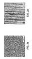
- FIG. 2 a ) and 2 b )show two morphologies or di-block polymers after their phase separation.
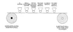
- FIG. 3is a manufacturing process flow diagram of mass production of a nanostructured conductive pattern.
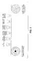
- FIG. 4is a series of schematics of various di-block copolymer morphologies that are spontaneously formed during their phase separation process.
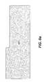
- FIG. 5shows a microreplicated structure
- FIG. 6( a )- 6 ( f )show a series of the exemplary process of making a wire grid polarizer.
- the inventionhas numerous advantages. We will illustrate the invention by specifically describing the details of the method to manufacture wire grid polarizer in a mass production process as an example.
- the inventionprovides a new method to manufacture different nanostructured patterns, for example, wire grid polarizer, on a patterned substrate.
- a manufacturing method for low cost fabrication of nano-scale metallic wire grid arrays on a flexible substrate such as PETis described, although such manufacturing method can be used on glass.
- These wire grid arrays of metalse.g. aluminum
- These di-block patternsare created on metallized plastic substrates, which may or may not be pre-coated with a random mixture of each polymer of the block copolymer compound.
- the metallized plastic substrate with or without the random polymer mixture coatingis previously patterned with alternating patches which are micro-replicated grooves/ledges or treated with the LCD type alignment process (e.g.
- compositions of di-block polymersare chosen to provide the desired surface features such as nanosized lamellar (wire) arrays.
- the templateis then subjected to post-fabrication steps such as cross-linking, to chemically and physically further distinguish the two polymeric components in the di-block.
- post-fabrication stepssuch as cross-linking, to chemically and physically further distinguish the two polymeric components in the di-block.
- One of the polymer compounds and the underlying metal layerare then removed in a spatially selective fashion by dissolution, etching, etc.
- the second polymer featureis subsequently removed by another dissolution or etching process to reveal the nano lamellar (wire) grid assembly on the plastic substrate.
- a plastic (e.g. PET) substratewith a topographic pattern of shallow, micro-grooves/ledges created by a micro-replication process to guide and direct the di-block copolymer self-assembly.
- the plastic substrateitself is of macroscopic dimensions and the grooves and ledges are microscopic in nature.
- the ledges and troughsare then uniformly coated with a thin layer of metal such as aluminum.
- a thin coating of a di-block copolymer of interestis then put on the metallized substrate.
- cylindrical rodsare formed from one of the polymers.
- the term “nano”refers to a characteristic size range, for example, of arrays, that are attained using the methods of self-assembly of copolymer molecules described herein.
- the wire diameter, the wire lengths and the period of the arraycan be in the nanosize range, that is, within a range of about a nanometer to over a thousand nanometers.
- Nano wirescan also refer to material that is not necessarily limited to electrically conductive, but is nevertheless useful when present in nanoscale arrays.
- the term “wire”refers to conductive material having width and length, where the aspect ratio (that is the ratio of length to width) is at least 2:1.
- multilevelrefers to structures that can be constructed by multiple, independent levels of lithography, with at least one level created with a laterally patterned diblock copolymer film.
- multilayeringwill refer to a structural element within a single layer of lithography that contains more than one material.
- FIG. 3The inventive manufacturing flow of the nanostructured conductive pattern is shown in FIG. 3 and illustrated in more detail in FIG. 6( a )- 6 ( f ).
- the substrateis made from polymer resins through extrusion.
- the substratecan be made of any optical polymeric material, although glass can also be used as a substrate. It can be radical polymer or condensation polymer. It can be hydrophobic or hydrophilic polymer. It can be any natural or synthetic polymer.
- the substrate polymer of the inventioncan be of different architecture: linear, grafted, branch or hyper branched.
- the polymermay be a thermoplastic.
- thermoplastic resinsare cellulose and its derivatives (cellulosic): cellulose ethers such as methyl cellulose, ethyl cellulose, hydroxyethyl cellulose, hydroxypropyl cellulose, and cyanoethyl cellulose, and cellulose esters such as triacetyl cellulose (TAC), diacetyl cellulose (DAC), cellulose acetate propionate (CAP), cellulose acetate butyrate (CAB), cellulose acetate phthalate, cellulose acetate trimellitate and cellulose nitrate.
- TACtriacetyl cellulose
- DACdiacetyl cellulose
- CAPcellulose acetate propionate
- CABcellulose acetate butyrate
- cellulose acetate phthalatecellulose acetate trimellitate and cellulose nitrate.
- the polymercan include polyolefins such as (linear) low and high density poly(ethylene), poly(propylene), chlorinated low density poly(ethylene), poly(4-methyl-1-pentene), and poly(ethylene) and cyclic polyolefins; poly(styrene); polyxylyene; polyimide; vinyl polymers and their copolymers such as poly(vinylcarbazole), poly(vinyl acetate), poly(vinyl alcohol), poly(vinyl chloride), poly(vinyl butyral), poly(vinylidene chloride), ethylene-vinyl acetate copolymers, and the like; polyacrylics their copolymers such as poly(ethyl acrylate), poly(n-butyl acrylate), poly(methylmethacrylate), poly(ethyl methacrylate), poly(n-butyl methacrylate), poly(n-propyl methacrylate), poly(acrylamide), polyacrylonitrile,
- Preferred substrate polymersinclude thermoplastic polymers such as polyester, vinyl, polystyrene, polyacrylic, and polyxylyene, polyvinylcarbazole, polyamide, polyimide, polycarbonate, polyether, polyketone, polyphenylene, polysulfide, polysulfone, and cyclic polyolefin. More preferred substrate polymer are PET and Bisphenol A polycarbonate.
- Substratescan be of different thickness ranging from 10 micron to 1 centimeter.
- the substrateis subjected to micropatterning process.
- a micropatternis generated on the substrate.
- Different micropatterning processcan be utilized.
- the pre-patterningcan be mechanical or other well established alignment techniques.
- the pre-patterningcan be due to the presence of micro-replicated ledges/grooves of an arbitrary, desired shape and form.
- Micro-replicationU.S. Pat. No. 6,800,234(B2X6)
- Another example of controlling surface energetics of the substrateis to use the alignment technique commonly used in the LCD industry, usually referred to as “rubbing”.
- pre-rubbingof the plastic substrate to align and direct the self-assembly of di-block copolymers structures.
- the method of using the pre-patterned substratedoes not preclude the use of other external forces, such as electric fields, magnetic fields, shear forces etc. to aid and expedite the alignment process.
- Itcan be also patterned using coatings of patches of hydrophobic and hydrophilic polymers. Preferably, it can be patterned with alternating patches, which are micro-replicated grooves/ledges.
- the micropatternis preferred to be a shallow regular array of grooves with flat bottom.
- the pitch of the groovesis preferred to be higher than 1 micron and less than 10 micron.
- the height of the groovesis preferred to be higher than 100 nm and less than 1 micron.
- the process of preparation of the wire grid polarizerinvolves conformally depositing a thin layer of conductive material on the micropatterned substrate.
- the conductive materialcan be different metals, transparent metal oxides or conducting polymers.
- Metalscan be Aluminum, Silver, Gold, Nickel and Copper.
- Metal oxidescan be indium tin oxide (ITO), and antimony tin oxide (AZO), etc.
- Conducting polymerscan be polythiophene, polyaniline, and polyacetylene and etc.
- the method depositionis corresponding to the material being deposited. It can be either vacuum process or ambient air process. It can be plasma, or sputtering. It can also be solution coating.
- the thickness of the conductive materialis larger than 50 nm and less than 1 micron. It is further preferred to be larger than 100 nm and less than 200 nm.
- a block copolymer that may or may not contain nanoparticlesis coated onto the aluminum coating and the ordered phase separation is formed during the drying of the coating or after the annealing of dried film.
- the drying of the polymer phasescan be achieved by several conventionally available methods.
- hot rollerswhich simultaneously apply directional pressure and shear and also heat.
- Heatcan also be applied by other means such as an IR source, microwave source, resistive wire coils, hot air or gas or a combination of both. Heat can be applied through radiation sources as well.
- Another examplecan be simultaneous application of an electric field when heat is applied to dry the polymer coatings.
- the heatcan be applied through heat rollers, which are electrified. If the rollers are not electrified, then the electric field may be applied by means commonly used such a corona device.
- the conceptis general in scope and is not limited to the nature of the application technique.
- Block Copolymers(Di-block, tri-block, tetra-block, star-block, graft-block) can be used for creation of periodic structures at the nanoscale (less than 100 nm). [Stoykovich et al., “Directed Assembly of Block Copolymer Blends into Nonregular Device-Oriented Structures”, Science 308, pp. 1442-1445 (2005)]
- Block Copolymers(Di-block, tri-block, tetra-block, star-block, graft-block) can be used for creation of periodic structures at the nanoscale (less than 100 nm). [Stoykovich et al., “directed Assembly of Block Copolymer Blends into Nonregular Device-Oriented Structures”, Science 308, pp. 1442-1445 (2005)]. Block copolymer is formed by linking two or more incompatible polymer chains together at the end. The phase separation is determined by the size of the polymer chain, typically tens of nanometers in size, and the interaction between the chains.
- the volume fraction of the componentscan be controlled and ordered morphologies, ranging from body-centered arrays of spherical domains (S) to hexagonally-packed cylindrical domains (C) to gyroids (G) to alternating lamellar domains (as shown in FIG. 4 ) spontaneously form when mobility is imparted to the chains.
- the phase inversionchanges as the volume ratio of the polymers change. Then the inversed hexagonally-packed cylindrical domains (C*), gyroids (G*), and the inversed spherical domains (S*) formed.
- the scanning force micrographshows cylinders of PMMA oriented normal to the films surface and the cylinders penetrate through the entire film.
- an alcohol rinsea standard industrial practice
- nanoporous filmis produced where the pore-size is identical to the size of the cylindrical domains of the original copolymer.
- Such nanoporous filmsare being used as templates for the fabrication of floating gates in flash memory applications and as scaffolds for the generation of nanoscopic magnetic elements for storage devices.
- the block copolymer suited for this inventioncan be of different chemical nature. It can be made from anionic, cationic or living radical polymerization.
- a block polymer of interestcan comprise more than one block. It can be diblock, triblock. tetra-block, star-block, and graft-block.
- One of the blockscan comprise random copolymer.
- One of the blockscan crystallize.
- One of the blockscan be liquid crystal.
- One of the blockscan be plastic at room temperature.
- One of the blockscan be rubbery at room temperature.
- One of the blockscan be hydrophobic.
- One of the blockscan be hydrophilic.
- polymerscan be used to form the block copolymer include but not limit to poly(styrene); polyxylyene; vinyl polymers such as poly(vinylcarbazole), poly(vinyl acetate), poly(vinyl alcohol), poly(vinyl chloride), poly(vinyl butyral), poly(vinylidene chloride), ethylene-vinyl acetate copolymers, and the like; polyacrylics such as poly(ethyl acrylate), poly(n-butyl acrylate), poly(methylmethacrylate), poly(ethyl methacrylate), poly(n-butyl methacrylate), poly(n-propyl methacrylate), poly(acrylamide), polyacrylonitrile, poly(acrylic acid), ethylene-acrylic acid copolymers; ethylene-vinyl alcohol copolymers; acrylonitrile copolymers; methyl methacrylate-styrene copolymers; ethylene-ethyl
- Some useful diblock copolymersare polystyrene-polymethylmethacrylate, polystyrene-polybutadiene, polystyrene-polyethylene oxide.
- the number molecular weightis in the range of 1000 to 100,000 g/mol and the volume fraction of one block is in the range of 0.3 to 0.7.
- a diblock copolymerphase-separates into a lamellar structure with the phase perpendicular to the plane of the substrate.
- the length of phase A and Bis 10 nm to 100 nm.
- the preferred length of phase A of the di-block copolymeris 10 to 20 nm and the preferred length of phase B is 20 to 50 nm.
- a useful di-block copolymerfor example, is made up of polystyrene-block-polybutadiene.
- Another useful diblock copolymeris polystyrene-b-poly(methyl methacrylate).
- the block copolymerformed lamellar structure with the periodic phase length of 15 nm. (Corvazier et al, J. Mater Chem, 2001, 11, 2864) It is also known that semi crystalline diblock copolymer tends to form lamellar structure.
- polymer A phaseis then removed by etching and or a dissolution process.
- polymer A phaseis poly(methyl methacrylate) (PMMA)
- polymer B phaseis polystyrene (PS).
- PMMApoly(methyl methacrylate)
- PSpolystyrene
- PMMAis a standard photoresist used routinely in the microelectronics industry.
- exposing the fills to ozonewill crosslink the PS (phase B polymer) and degrade the poly (butadiene) (Phase A polymer).
- the minor component comprising the nanoscopic cylindrical domainscan be selectively removed.
- the present inventionthen requires the removal of the aluminum, or other conductive material underneath the phase A polymer by an etch process using the segments of remaining polymer (resist) as a mask.
- the criterion for a good etch processis to have a large window for the parameters such as etch time and the degradation of the resist.
- the etch processcan be divided into two methods; dry and wet.
- wet aluminum etchesthe components are phosphoric, acetic, and nitric acid (PAN etch). These components can be varied to achieve different etch rates and selectivity with other metals which may be present.
- PAN etchnitric acid
- Wet etchessuffer from the fact that they are very isotropic. What this yields is a sloped profile due to undercutting of the polymeric resist mask. It is difficult to get very high aspect ratios using wet etches on non-crystalline materials.
- Reactive ion etchinguses microwaves to generate a plasma in a low-pressure gas.
- the gashas a component which, when excited, can generate reactive species such as radicals and ions.
- the ionscan be accelerated to electrodes.
- the sampleis in close proximity to the one of the electrodes.
- the ionsare thus directed at a specific angle, usually vertical, onto the sample. The ions react with the surface and chemically etch the material.
- Aluminumis usually reactive ion etched with a halogen-based plasma.
- Carbon tetrachloride or chloroformserve as a halogen precursor and is mixed with an inert gas.
- the plasmagenerates chlorine radical ions, which react with aluminum to form volatile aluminum trichloride.
- This type of aluminum etchingcan give high aspect ratio walls due to the anisotropy if the ion flow direction. Since chloride radical ions react slowly with most organics to create volatile species, the resist gives good discrimination during the etching.
- a conductive patternis formed on a micropatterned substrate by removing Polymer B.
- the inventionis also general in the sense, we could visualize use of several shapes and sizes of grooves on the plastic substrate, to guide and direct self-assembly of di-block copolymer phase separation features, such as circles, triangles, cylinders, pyramids, etc. which can be subsequently used as templates/masks to deposit spatially arranged materials of practical interest such as metals, semi-conductors magnetic materials etc.
- the inventioncan be generalized to use one of the polymers in the block copolymer as a functional feature itself. By pre-filling the copolymers with nanomaterials with specific properties, one can creating nano-features with novel properties, for example, metallic, semi-conducting or insulating and removing one of the polymers. These ordered nano-features may or may not be positioned on conductive surfaces.
- a sheet or roll of flexible plastic such as PETis pre-patterned by the micro-replication process to yield an array of rectangular grooves as shown in FIG. 5 and FIG. 6( a ).
- P, W and Dspecify the pitch, wall width and height of the grooves and the grooves run across the entire length of the flexible substrate which arbitrary and/or determined by manufacturing capabilities.
- the pitch (P) of the groovescan vary anywhere from 1 micron to 100 micron but preferably in the 5 micron to 25 micron range.
- the wall width (W) of the groovecan range from 0.5 micron to 25 micron, preferably in the 1 micron to 10-micron range.
- the depth of the groove (D)can range from 0.25 micron to 5 micron, preferably in the 0.5 micron to 1-micron range.
- the flexible sheet or rollis then coated in a conformal fashion with a thin layer of metal, preferably aluminum ( FIG. 6( b )).
- the thickness of the metal layercan range from 0.05 micron to 0.5 micron, preferably in the range of 0.1 micron to 0.2 micron.
- the conformal nature of the coatingresults in the metal coating filling the troughs and ledges of the grooves such as to replicate the micro-replicated pattern.
- the metal filmis then coated with a thin layer of the copolymer mixture (A, B) ( FIG. 6( c )).
- the coating thicknesscan range from 0.01 micron to 0.1 micron, preferably in the range of 0.02 micron to 0.05 micron.
- the coatingis once again conformal in nature such as to replicate the micro-replicated pattern.
- the copolymer coatingis then coated with a thin film of the di-block copolymer.
- the components (A,B) of the di-block copolymerare the same as the components in the copolymer mixture.
- the thickness of the di-block copolymercan range from 0.05 micron to 1 micron, preferably between 0.1 micron to 0.25 micron.
- a block copolymer including a component that can be cross-linkedis desirable.
- This componentcan be cross-linked before or during removal of another component, and can therefore add structural integrity to the copolymer.
- This componentcan be referred to as the matrix component.
- Suitable matrix componentsinclude polystyrene, polybutadiene, polydimethylsiloxane, and other polymers.
- the component that is to be removedcan be called the core component.
- Suitable core componentsinclude polymethylmethacrylate, polybutadiene, polycaprolactone or a photoresist.
- Any block copolymerscan be used, such as alkyl/alkyl, alkyl/aryl, aryl/aryl, hydrophilic/hydrophilic, hydrophilic/hydrophobic, hydrophobic/hydrophobic-, positively or negatively charged/positively or negatively charged, uncharged/positively or negatively charged, or uncharged/uncharged.
- the copolymersmay be containing nanoparticle, which may be metallic, semi-conducting or insulating in nature. Some examples of nanoparticles are gold, silver, cadmium selenide, silicon, zinc sulphide etc.
- the nanoparticlesmay be chosen such that during the phase separation of the polymers, the nanoparticles may or may not preferentially segregate into one polymer.
- the copolymersmay be containing biological materials such as DNA.
- the copolymerscan be coated from a common solvent or a mixture of co-solvents.
- the sandwich structurecan be heated above the glass transition temperature of the copolymer.
- one of the components (e.g. core) of the di-block copolymer of the substrate-associated copolymeris removed. Removal of the component is achieved, e.g., by exposure to radiation (ultraviolet light, x-ray radiation, gamma radiation, visible light, heat, or an electron beam or any other radiation source which selectively degrades the minor component). Degradation or decomposing agents such as reactive oxygen species, including for example, ozone, or solvents such as ethanol, can also be used. Ultraviolet light can be used to degrade, for example, polymethylmethacrylate as a core component. Ethanol can be used to degrade, for example, polybutadiene.
- a step to remove any residual componentcan include treatment with a liquid, including washing with a solvent, or a material that reacts preferentially with the residual component, such as an acid or a base.
- the material used to react with residual degraded componentcan be, for example, a dilute form of acetic acid.
- the same solvent or another solvent or etching solutionis used to dissolve the metal. For example, sodium hydroxide can be used to etch aluminum ( FIG. 6( e )).
- the remaining volumeis occupied by the remainder copolymer component and is referred to as the matrix.
- Cross-linking of a component that is not degraded by an energy source or agentcan add structural strength to the film.
- a copolymer componentis cross-linked simultaneously with the degradation of another copolymer component.
- the radiationcan optionally and desirably crosslink and substantially immobilize the matrix component of the diblock copolymer, so that the matrix maintains the array structure even after the rectangular parallelepiped voids are created.
- a nanoporous array templateis the resulting overall structure.
- the width of the apertures/voidscan range from about 5 nm to about 500 nm or more, and the periodicity can range from about 5.0 to 500 nm.
- the final step ( FIG. 6 (f)) of the manufacturing processrequires the matrix component of the di-block copolymer and any underlying copolymer coating to be removed by dissolution in an appropriate solvent or by radiation, etc. This process reveals a nanoarray of metal wires (e.g. aluminum), which could be used as light polarizers.
- metal wirese.g. aluminum
Landscapes
- Engineering & Computer Science (AREA)
- Physics & Mathematics (AREA)
- Chemical & Material Sciences (AREA)
- Nanotechnology (AREA)
- General Physics & Mathematics (AREA)
- Optics & Photonics (AREA)
- Crystallography & Structural Chemistry (AREA)
- Biophysics (AREA)
- Life Sciences & Earth Sciences (AREA)
- Condensed Matter Physics & Semiconductors (AREA)
- Manufacturing & Machinery (AREA)
- Computer Hardware Design (AREA)
- Microelectronics & Electronic Packaging (AREA)
- Power Engineering (AREA)
- Laminated Bodies (AREA)
- Polarising Elements (AREA)
- Treatments Of Macromolecular Shaped Articles (AREA)
Abstract
Description
- This application relates to commonly assigned, copending applications filed simultaneously herewith: U.S. patent application Ser. No. ______ (Doc. # 92866) “WIRE GRID POLARIZER”.
- The present invention is related to the nanostructured pattern formed from block copolymers, and is related to using these nanostructured features of the block copolymers as template to form nanoscale, ordered functional features on flexible substrates and is also related to using the nanostructured features of one of the polymer phases in the copolymer to be the ordered functional feature(s) itself and is also related to filling the copolymers with nanomaterials and using the nanostructured features of one of the filled polymer phases in the copolymer to be the ordered functional feature(s) itself. The present invention is also related specifically to the low cost manufacture of a conductive wire grid polarizer on flexible substrates. The present invention is also related specifically to the creation of an array of metal wires, of any shape, with a long-range order in at least in one direction, with a periodicity in the nanometer length scale in that dimension. The diameter or height of the wires is in the nanometer size and the lengths could be several micrometers.
- The processes that are currently available to produce nanoscale patterns on substrates are vacuum based technologies and are generally expensive. Moreover, the photolithographic technologies used in these processes have generally a lower limit in terms of resolution of the nanoscale patterns, which is imposed by the wavelength of light. New technological approaches are taken to reduce both the cost and feature size. A very promising new technology is the directed self-assembly of di-block co-polymers to create fine nanoscale patterns on substrates at ambient conditions.
- A key aspect of this technology is the term “directed self-assembly”. The process generally involves coating the di-block polymers on a substrate under the influence of a directional force. The directional force can be as simple as a confinement space whose dimensions are comparable to the dimensions of the desired nanoscale patterns, or an electric or magnetic field. It could be an electrostatic field manifest as hydrophobic or hydrophilic features on the substrate.
- By directing the self-assembly of the elements and by biasing the arrangement of the arrays on a surface, unprecedented aerial densities of nanoscale features can be achieved. When block copolymers of polystyrene-b-poly (ethylene oxide) were coated onto a silicon substrate where trenches (about 2 micron in width) were photo lithographically placed on a surface, within each trench are arrays of hexagonally packed, nanoscopic cylindrical domains where each cylinder is ˜20 nm in size and each array is in orientational registry with the arrays in adjoining trenches. Most importantly is the fact that the block copolymer, by controlling the preparation conditions, self-assembled into the structure shown with no external manipulation of the morphology.
- Nealey and coworkers at the University of Wisconsin (Kim, S. O.; Solak, H. H.; Stoykovich, M. P.; Ferrier, N. J.; de Pablo, J. J.; Nealey, P. F.; Nature, 2003, 424, 411) took an alternate approach in controlling the lateral placement of these nanoscopic domains. They coated block copolymer of polystyrene-b-poly (methyl methacrylate) onto a surface that was patterned using soft x-rays. The surface patterning was done on a size scale commensurate with the size of the copolymer domains and each domain was directed on the surface. Without patterning, the lamellar domains (in this case) were randomly oriented on the surface. With patterning a precise distribution of the domains across the surface was achieved.
- We will discuss in detail, a very specific product, known as the wire grid polarizer. Wire grid polarizers have been used in projection displays as pre-polarizers, analyzers, and polarizing beam splitters [1-3]. They have many advantages, including high heat and high light flux tolerance. They have also been used as reflective polarizers for polarization recycling [4-6]. A low fill-factor wire grid polarizer is disclosed in copending patent application to Mi et al., US Patent Application No. 2006/0061862. The following additional references are background for the present invention.
- [1] E. Hansen, E. Gardner, R. Perkins, M. Lines, and A. Robbins, “The Display Applications and Physics of the ProFlux Wire Grid Polarizer”, SID 2002 Symposium Digest Vol. 33, pp. 730-733, (2002).
- [2] A. F. Kurtz, B. D. Silverstein, and J. M. Cobb, “Digital Cinema Projection with R-LCOS Displays”, SID 2004 Symposium Digest Vol. 35, pp. 166-169, (2004).
- [3] J. Chen, M. Robinson, and G. Sharp, “General Methodology for LCoS panel Compensation”, SID 2004 Symposium Digest Vol. 35, pp. 990-993, (2004).
- [4] T. Sergan, J. Kelly, M. Lavrentovich, E. Gardner, D. Hansen, R. Perkins, J. Hansen, and R. Critchfield, “Twisted Nematic Reflective Display with Internal Wire Grid Polarizer”, SID 2002 Symposium Digest Vol. 33, pp. 514-517, (2002).
- [5] J. Grinberg, and M. Little, “Liquid Crystal Device”, U.S. Pat. No. 4,688,897 (1987).
- [6] D. Hansen, and J. Gunther, “Dual Mode Reflective/Transmissive Liquid Crystal Display Apparatus”, U.S. Pat. No. 5,986,730 (1999).
- A wire grid polarizer is schematically shown in
FIG. 1 , where P, W, and H specify the pitch, width, and height of the wires, respectively. Ideally, the pitch P of the wires should be as small as possible and should be less than ⅓ of the wavelength of interest. It is only limited by manufacturing processes. For a wire grid polarizer designed for the use of visible light, the pitch is ˜140 nm, and the height is also ˜140 nm. The wires are made of aluminum, which has superior optical properties. When unpolarized light is incident upon the wire grid polarizer, light of S-polarization (parallel to the wires) is reflected back, and light of P-polarization (perpendicular to the wires) is transmitted. The wire grid polarizers have been fabricated using by commonly known processes. For example, both Garvin, in U.S. Pat. No. 4,049,944, and Ferrante, in U.S. Pat. No. 4,514,479, describe the use of holographic interference lithography to form a fine grating structure in photoresist, followed by ion beam etching to transfer the structure into an underlying metal film. Stenkamp (“Grid Polarizer For The Visible Spectral Region”, Proceedings of the SPIE, vol. 2213, pages 288-296) describes the use of direct e-beam lithography to create the resist pattern, followed by reactive ion etching to transfer the pattern into a metal film. Other high-resolution lithography techniques, including extreme ultraviolet lithography and X-ray lithography could also be used to create the resist pattern. Other techniques, including other etching mechanisms and lift-off processes, could be used to transfer the pattern from the resist to a metal film. - The above processes have the following problems:
- 1) In general, the pitch of the wire grid polarizer is preferred to be as small as possible for better optical performance in terms of transmission and reflection, acceptance angle, and spectral dependence. However, the pitch that can be achieved is fundamentally limited by the wavelength of the light source and the index of refraction of the photoresist used in corresponding lithography techniques. A wire grid polarizer of short pitch requires a light source with short wavelength and a photoresist with low index of refraction, but they are not readily available for meeting the ever-growing requirement of shorter pitch.
- 2) The above processes require a rigid glass substrate to hold the metal wires and photoresist. Though rigid and flat, plastic substrates might be used to replace the glass substrate, the high temperature and chemicals used in the subsequent process make most plastic substrates difficult to use.
- What is needed, therefore, is a method of forming a wire grid polarizer in mass production.
- Generally, it would be desirable to form a nanostructured pattern of a functional material. Furthermore, it would be desirable to form a nanostructured pattern of a functional material, which has been filled with nanoparticles, which are magnetic, conductive, semi-conductive or insulating with desirable optical properties such as refractive index, photoluminescence, etc.
- It would also be desirable to form nanostructured patterns of a functional material containing desirable biological properties. Furthermore, it would be desirable to have these nanostructures with specific reactive species, which upon exposure to certain environment would, by a physical, chemical or biological reaction, create a nanopatterned structure of a new set of species, which are produced through this reaction.
- Specifically, it would be desirable to form a nanostructured conductive pattern. It would be desirable to form a nanostructured pattern using continuous process. Furthermore, it would be desired to form a nanostructured aluminum pattern on a substrate, which can be used as a wire grid polarizer. Furthermore, it would be desired to form a wire grid polarizer with low fill factor.
- It is an object of the invention to form a nanostructured pattern of functional material on a substrate.
- It is an object of the invention to form a nanostructured pattern of a functional material, which is inorganic, organic or polymeric on a substrate.
- It is an object of the invention to form a nanostructured pattern of a functional material, which is inorganic, organic or polymeric and containing nanoparticles which can be magnetic, conductive, semi-conductive, or insulating, on a substrate.
- It is an object of the invention to form a nanostructured pattern of a biological functional material such as DNA, on a substrate.
- It is an object of the invention to form a nanostructured pattern of a functional material, which is inorganic, organic, polymeric or biologic which can be activated to react and produce a new nanopatterned species, on a substrate.
- It is an object of the invention to form a nanostructured conductive pattern on a substrate.
- It is another object to provide a method of forming nanostructured patterns of mass production.
- It is a further object to form nanostructured patterns such as a wire grid polarizer using a mass production process.
- It is a further object to form a wire grid polarizer of low fill factor.
- These and other objects of the invention are accomplished by a method of forming a pattern on a substrate comprising providing a substrate, coating said substrate with a functional material, coating said functional layer with a block copolymer of at least an A and B polymer chains with or without nanoparticles, drying said block copolymer to form ordered nano-domains, removing the A polymer phase of the dried block copolymer and the area of the functional material below the phase removed.
- The invention relates to a method of forming a nanostructured pattern on a substrate. The steps include providing a substrate and coating the substrate with functional material to form a layer of functional material. A block copolymer of at least an A polymer chain and a B polymer chain is coated on the functional material to forma a layer. The block copolymer is dried to form ordered nanodomains. The A polymer chain of the dried block copolymer is removed to form voids and the functional material is then removed from where the A polymer chain has been removed.
- The invention provides a low cost production method of nanostructured functional materials such as wire grid polarizer. The invention also provides a general method to produce nanostructured conductive, semi-conductive, magnetic, insulating or biologic patterns. The technique described here for creating nano scale arrays is significantly advantaged with respect to conventional vacuum based processes currently used to create them. The techniques are amenable to manufacture, in that they are simple, fast, and cost-effective. They are readily adoptable by industry and compatible with other fabrication processes. The techniques described herein significantly advance the general utility of nanofabrication by self-assembling copolymer templates.
- The invention also provides a low cost production method for creating high aerial density of nanoscale features of different shapes and forms on a flexible substrate, under ambient conditions. There is no other competing technology currently available which is capable of providing such features at low cost. This technology uses currently available manufacturing capabilities in an innovative manner to rapidly bring to market a truly low cost nanofabrication technology, which does not exist right now. The potential product applications are electronic display devices such as television, mobile phones and electronic products such as digital music systems, computers etc.
- This is especially important in the current global market place where a new “lower middle class” consumer base which is five times larger in size compared to the current middle class numbers, is being created.
- Other features and advantages of the invention will be apparent from the following detailed description, and from the claims.
FIG. 1 is a schematic view of a wire grid polarizer.FIG. 2 a) and2b) show two morphologies or di-block polymers after their phase separation.FIG. 3 is a manufacturing process flow diagram of mass production of a nanostructured conductive pattern.FIG. 4 is a series of schematics of various di-block copolymer morphologies that are spontaneously formed during their phase separation process.FIG. 5 shows a microreplicated structureFIG. 6( a)-6(f) show a series of the exemplary process of making a wire grid polarizer.- For a better understanding of the present invention along with other objects, advantages and capabilities thereof, reference is made to the following description and appended claims in connection with the above-described drawings.
- The invention has numerous advantages. We will illustrate the invention by specifically describing the details of the method to manufacture wire grid polarizer in a mass production process as an example. The invention provides a new method to manufacture different nanostructured patterns, for example, wire grid polarizer, on a patterned substrate.
- A manufacturing method for low cost fabrication of nano-scale metallic wire grid arrays on a flexible substrate such as PET is described, although such manufacturing method can be used on glass. These wire grid arrays of metals (e.g. aluminum) are useful as optical polarizers. This is accomplished by patterning block copolymer templates with selective exposure to a radiation source. These di-block patterns are created on metallized plastic substrates, which may or may not be pre-coated with a random mixture of each polymer of the block copolymer compound. The metallized plastic substrate with or without the random polymer mixture coating is previously patterned with alternating patches which are micro-replicated grooves/ledges or treated with the LCD type alignment process (e.g. rubbing) to induce certain ordering tendencies on the surface for the di-block copolymers during their phase segregation. All these pre-treatment procedures guide and direct the phase separating features on the plastic substrate to align in an ordered fashion. The compositions of di-block polymers are chosen to provide the desired surface features such as nanosized lamellar (wire) arrays.
- The template is then subjected to post-fabrication steps such as cross-linking, to chemically and physically further distinguish the two polymeric components in the di-block. One of the polymer compounds and the underlying metal layer are then removed in a spatially selective fashion by dissolution, etching, etc. The second polymer feature is subsequently removed by another dissolution or etching process to reveal the nano lamellar (wire) grid assembly on the plastic substrate.
- In one aspect of the invention, we use a plastic (e.g. PET) substrate with a topographic pattern of shallow, micro-grooves/ledges created by a micro-replication process to guide and direct the di-block copolymer self-assembly. The plastic substrate itself is of macroscopic dimensions and the grooves and ledges are microscopic in nature. The ledges and troughs are then uniformly coated with a thin layer of metal such as aluminum. A thin coating of a di-block copolymer of interest is then put on the metallized substrate. In the case of the cylindrical forming di-block copolymer, cylindrical rods are formed from one of the polymers. It has been shown that the self assembling of the di-block copolymer and the orientation of one of the phases can be controlled topologically. Nealey and coworkers at the University of Wisconsin coated a block copolymer of polystyrene-b-poly (methyl methacrylate) onto a surface that was patterned using soft x-rays. The surface patterning was done on a size scale commensurate with the size of the copolymer domains and each domain was directed on the surface. Without patterning, the lamellar domains (in this case) were randomly oriented on the surface (
FIG. 2( a)). With patterning a precise distribution of the domains across the surface was achieved (FIG. 2( b)). The substrate topography influences and aligns the orientation of the phase separating polymer blocks in the direction of the grooves and ledges. External forces, such as electrostatic, magnetic, fluid shear etc. may be applied during the phase separation process to expedite the process at lower temperatures. - As used herein, the term “nano” refers to a characteristic size range, for example, of arrays, that are attained using the methods of self-assembly of copolymer molecules described herein. For example, the wire diameter, the wire lengths and the period of the array can be in the nanosize range, that is, within a range of about a nanometer to over a thousand nanometers. “Nano wires” can also refer to material that is not necessarily limited to electrically conductive, but is nevertheless useful when present in nanoscale arrays. As used herein, the term “wire” refers to conductive material having width and length, where the aspect ratio (that is the ratio of length to width) is at least 2:1. In this application, the term “multilevel” refers to structures that can be constructed by multiple, independent levels of lithography, with at least one level created with a laterally patterned diblock copolymer film. As used herein, the term “multilayering” will refer to a structural element within a single layer of lithography that contains more than one material.
- The inventive manufacturing flow of the nanostructured conductive pattern is shown in
FIG. 3 and illustrated in more detail inFIG. 6( a)-6(f). - The substrate is made from polymer resins through extrusion. The substrate can be made of any optical polymeric material, although glass can also be used as a substrate. It can be radical polymer or condensation polymer. It can be hydrophobic or hydrophilic polymer. It can be any natural or synthetic polymer. The substrate polymer of the invention can be of different architecture: linear, grafted, branch or hyper branched. The polymer may be a thermoplastic. Illustrative of useful thermoplastic resins are cellulose and its derivatives (cellulosic): cellulose ethers such as methyl cellulose, ethyl cellulose, hydroxyethyl cellulose, hydroxypropyl cellulose, and cyanoethyl cellulose, and cellulose esters such as triacetyl cellulose (TAC), diacetyl cellulose (DAC), cellulose acetate propionate (CAP), cellulose acetate butyrate (CAB), cellulose acetate phthalate, cellulose acetate trimellitate and cellulose nitrate. The polymer can include polyolefins such as (linear) low and high density poly(ethylene), poly(propylene), chlorinated low density poly(ethylene), poly(4-methyl-1-pentene), and poly(ethylene) and cyclic polyolefins; poly(styrene); polyxylyene; polyimide; vinyl polymers and their copolymers such as poly(vinylcarbazole), poly(vinyl acetate), poly(vinyl alcohol), poly(vinyl chloride), poly(vinyl butyral), poly(vinylidene chloride), ethylene-vinyl acetate copolymers, and the like; polyacrylics their copolymers such as poly(ethyl acrylate), poly(n-butyl acrylate), poly(methylmethacrylate), poly(ethyl methacrylate), poly(n-butyl methacrylate), poly(n-propyl methacrylate), poly(acrylamide), polyacrylonitrile, poly(acrylic acid), ethylene-acrylic acid copolymers; ethylene-vinyl alcohol copolymers; acrylonitrile copolymers; methyl methacrylate-styrene copolymers; ethylene-ethyl acrylate copolymers; methacrylated butadiene-styrene copolymers, and the like; polycarbonates such as poly(methane bis(4-phenyl) carbonate), poly(1,1-ether bis(4-phenyl) carbonate), poly(diphenylmethane bis(4-phenyl)carbonate), poly(1,1-cyclohexane bis(4-phenyl)carbonate), poly(2,2-bis-(4-hydroxyphenyl)propane)carbonate and the like; polyether; polyketone; polyphenylene; polysulfide; polysulfone; polylactones such as poly(pivalolactone), poly(caprolactone) and the like; polyurethanes; linear long-chain diols such as poly(tetramethylene adipate), poly(ethylene adipate), poly(1,4-butylene adipate), poly(ethylene succinate), poly(2,3-butylenesuccinate), polyether diols and the like; polyether ether ketones; polyamides such as poly(4-amino butyric acid), poly(hexamethylene adipamide), poly(6-aminohexanoic acid), poly(m-xylylene adipamide), poly(p-xylyene sebacamide), poly(2,2,2-trimethyl hexamethylene terephthalamide), poly(metaphenylene isophthalamide) (Nomex™), poly(p-phenylene terephthalamide)(Kevlar™), and the like; polyesters such as poly(ethylene azelate), poly(ethylene-1,5-naphthalate), poly(ethylene-2,6-naphthalate), poly(1,4-cyclohexane dimethylene terephthalate), poly(ethylene oxybenzoate) (A-Tell™), poly(para-hydroxy benzoate) (Ekonol™), poly(1,4-cyclohexylidene dimethylene terephthalate) (Kodel™) (cis), poly(1,4-cyclohexylidene dimethylene terephthalate) (Kodel™) (trans), polyethylene terephthlate, polybutylene terephthalate and the like; poly(arylene oxides) such as poly(2,6-dimethyl-1,4-phenylene oxide), poly(2,6-diphenyl-1,4-phenylene oxide) and the like; poly(arylene sulfides) such as poly(phenylene sulfide) and the like; polyetherimides; ionomers; poly(epichlorohydrins); furan resins such as poly(furan); silicones such as poly(dimethyl siloxane), poly(dimethyl siloxane), poly(dimethyl siloxane co-phenylmethyl siloxane) and the like; polytetrafluoroethylene; and polyacetals. Copolymers and/or mixtures of these aforementioned polymers can also be used.
- Preferred substrate polymers include thermoplastic polymers such as polyester, vinyl, polystyrene, polyacrylic, and polyxylyene, polyvinylcarbazole, polyamide, polyimide, polycarbonate, polyether, polyketone, polyphenylene, polysulfide, polysulfone, and cyclic polyolefin. More preferred substrate polymer are PET and Bisphenol A polycarbonate.
- Substrates can be of different thickness ranging from 10 micron to 1 centimeter.
- The substrate is subjected to micropatterning process. A micropattern is generated on the substrate. Different micropatterning process can be utilized. The pre-patterning can be mechanical or other well established alignment techniques. For example, the pre-patterning can be due to the presence of micro-replicated ledges/grooves of an arbitrary, desired shape and form. Micro-replication (U.S. Pat. No. 6,800,234(B2X6)) is a generally recognized, low cost way to topographically pattern a flexible substrate. Another example of controlling surface energetics of the substrate is to use the alignment technique commonly used in the LCD industry, usually referred to as “rubbing”. In this specific invention we would use “pre-rubbing” of the plastic substrate to align and direct the self-assembly of di-block copolymers structures. The method of using the pre-patterned substrate does not preclude the use of other external forces, such as electric fields, magnetic fields, shear forces etc. to aid and expedite the alignment process. It can be also patterned using coatings of patches of hydrophobic and hydrophilic polymers. Preferably, it can be patterned with alternating patches, which are micro-replicated grooves/ledges. The micropattern is preferred to be a shallow regular array of grooves with flat bottom. The pitch of the grooves is preferred to be higher than 1 micron and less than 10 micron. The height of the grooves is preferred to be higher than 100 nm and less than 1 micron.
- In the present invention the process of preparation of the wire grid polarizer involves conformally depositing a thin layer of conductive material on the micropatterned substrate. The conductive material can be different metals, transparent metal oxides or conducting polymers. Metals can be Aluminum, Silver, Gold, Nickel and Copper. Metal oxides can be indium tin oxide (ITO), and antimony tin oxide (AZO), etc. Conducting polymers can be polythiophene, polyaniline, and polyacetylene and etc. The method deposition is corresponding to the material being deposited. It can be either vacuum process or ambient air process. It can be plasma, or sputtering. It can also be solution coating. The thickness of the conductive material is larger than 50 nm and less than 1 micron. It is further preferred to be larger than 100 nm and less than 200 nm.
- As a next step in the preparation of the wire grid polarizer by our process, a block copolymer that may or may not contain nanoparticles is coated onto the aluminum coating and the ordered phase separation is formed during the drying of the coating or after the annealing of dried film.
- The drying of the polymer phases can be achieved by several conventionally available methods. For example, hot rollers, which simultaneously apply directional pressure and shear and also heat. Heat can also be applied by other means such as an IR source, microwave source, resistive wire coils, hot air or gas or a combination of both. Heat can be applied through radiation sources as well. Another example can be simultaneous application of an electric field when heat is applied to dry the polymer coatings. The heat can be applied through heat rollers, which are electrified. If the rollers are not electrified, then the electric field may be applied by means commonly used such a corona device. We can conceive of applying heat, electric field and shear forces simultaneously as well by combinations of techniques such as the ones listed above. The concept is general in scope and is not limited to the nature of the application technique.
- Block Copolymers (Di-block, tri-block, tetra-block, star-block, graft-block) can be used for creation of periodic structures at the nanoscale (less than 100 nm). [Stoykovich et al., “Directed Assembly of Block Copolymer Blends into Nonregular Device-Oriented Structures”, Science 308, pp. 1442-1445 (2005)]
- Block Copolymers (Di-block, tri-block, tetra-block, star-block, graft-block) can be used for creation of periodic structures at the nanoscale (less than 100 nm). [Stoykovich et al., “directed Assembly of Block Copolymer Blends into Nonregular Device-Oriented Structures”, Science 308, pp. 1442-1445 (2005)]. Block copolymer is formed by linking two or more incompatible polymer chains together at the end. The phase separation is determined by the size of the polymer chain, typically tens of nanometers in size, and the interaction between the chains. By changing the length of the chains linked together, the volume fraction of the components can be controlled and ordered morphologies, ranging from body-centered arrays of spherical domains (S) to hexagonally-packed cylindrical domains (C) to gyroids (G) to alternating lamellar domains (as shown in
FIG. 4 ) spontaneously form when mobility is imparted to the chains. The phase inversion changes as the volume ratio of the polymers change. Then the inversed hexagonally-packed cylindrical domains (C*), gyroids (G*), and the inversed spherical domains (S*) formed. - In thin films, by controlling the orientation of these domains and by selectively removing one of the components by standard photolithographic processes or by use of phase selective chemistries, a wealth of opportunities emerge for the use of these arrays of nanoscopic elements as templates and scaffolds for the fabrication of novel devices and structures. The control over the orientation of these elements rests in controlling the thickness of the film relative to the period of the block copolymer morphology (commensurability) and manipulating the manner in which the two blocks interact with the underlying substrate and surface. For example, when a spin-coated film of a polystyrene-b-poly (methyl methacrylate) diblock copolymer was placed on a passivated silicon substrate and heated above its glass transition temperature, the scanning force micrograph shows cylinders of PMMA oriented normal to the films surface and the cylinders penetrate through the entire film. Upon exposure to UV radiation and an alcohol rinse (a standard industrial practice) a nanoporous film is produced where the pore-size is identical to the size of the cylindrical domains of the original copolymer. Such nanoporous films are being used as templates for the fabrication of floating gates in flash memory applications and as scaffolds for the generation of nanoscopic magnetic elements for storage devices.
- The block copolymer suited for this invention can be of different chemical nature. It can be made from anionic, cationic or living radical polymerization. A block polymer of interest can comprise more than one block. It can be diblock, triblock. tetra-block, star-block, and graft-block. One of the blocks can comprise random copolymer. One of the blocks can crystallize. One of the blocks can be liquid crystal. One of the blocks can be plastic at room temperature. One of the blocks can be rubbery at room temperature. One of the blocks can be hydrophobic. One of the blocks can be hydrophilic. Examples of polymers can be used to form the block copolymer include but not limit to poly(styrene); polyxylyene; vinyl polymers such as poly(vinylcarbazole), poly(vinyl acetate), poly(vinyl alcohol), poly(vinyl chloride), poly(vinyl butyral), poly(vinylidene chloride), ethylene-vinyl acetate copolymers, and the like; polyacrylics such as poly(ethyl acrylate), poly(n-butyl acrylate), poly(methylmethacrylate), poly(ethyl methacrylate), poly(n-butyl methacrylate), poly(n-propyl methacrylate), poly(acrylamide), polyacrylonitrile, poly(acrylic acid), ethylene-acrylic acid copolymers; ethylene-vinyl alcohol copolymers; acrylonitrile copolymers; methyl methacrylate-styrene copolymers; ethylene-ethyl acrylate copolymers; methacrylated butadiene-styrene copolymers, and the like; polydiene such as poly(butadiene), poly(isobutylene), poly isoprene, polyether such as polyethylene oxide, polypropylene oxide and the like; polyol such as polyvinyl alcohol and the like, polyvinyl acetate and acetal. Examples of diblock copolymer include polystyrene-acrylate. The acrylate can be methylmethacrylate.
- Some useful diblock copolymers are polystyrene-polymethylmethacrylate, polystyrene-polybutadiene, polystyrene-polyethylene oxide. The number molecular weight is in the range of 1000 to 100,000 g/mol and the volume fraction of one block is in the range of 0.3 to 0.7.
- In one embodiment, a diblock copolymer phase-separates into a lamellar structure with the phase perpendicular to the plane of the substrate. The length of phase A and B is 10 nm to 100 nm. The preferred length of phase A of the di-block copolymer is 10 to 20 nm and the preferred length of phase B is 20 to 50 nm. A useful di-block copolymer, for example, is made up of polystyrene-block-polybutadiene. Another useful diblock copolymer is polystyrene-b-poly(methyl methacrylate). With a number molecular weight of 14,600 and a volume fraction of 0.5 of polystyrene, the block copolymer formed lamellar structure with the periodic phase length of 15 nm. (Corvazier et al, J. Mater Chem, 2001, 11, 2864) It is also known that semi crystalline diblock copolymer tends to form lamellar structure.
- The polymer A phase is then removed by etching and or a dissolution process. In the case of polystyrene-b-poly (methyl methacrylate), polymer A phase is poly(methyl methacrylate) (PMMA) and polymer B phase is polystyrene (PS). By exposing the film to UV radiation, polymer A phase, PMMA, is decomposed and polymer B phase, PS, is cross-linked. PMMA is a standard photoresist used routinely in the microelectronics industry. In the case of polystyrene-b-poly (butadiene), exposing the fills to ozone will crosslink the PS (phase B polymer) and degrade the poly (butadiene) (Phase A polymer). In numerous other block copolymer systems, the minor component comprising the nanoscopic cylindrical domains can be selectively removed.
- The present invention then requires the removal of the aluminum, or other conductive material underneath the phase A polymer by an etch process using the segments of remaining polymer (resist) as a mask. The criterion for a good etch process is to have a large window for the parameters such as etch time and the degradation of the resist. The etch process can be divided into two methods; dry and wet.
- In wet aluminum etches, the components are phosphoric, acetic, and nitric acid (PAN etch). These components can be varied to achieve different etch rates and selectivity with other metals which may be present. Wet etches suffer from the fact that they are very isotropic. What this yields is a sloped profile due to undercutting of the polymeric resist mask. It is difficult to get very high aspect ratios using wet etches on non-crystalline materials.
- The most common dry etch process for aluminum is reactive ion etching (RIE). Reactive ion etching uses microwaves to generate a plasma in a low-pressure gas. The gas has a component which, when excited, can generate reactive species such as radicals and ions. The ions can be accelerated to electrodes. Typically the sample is in close proximity to the one of the electrodes. The ions are thus directed at a specific angle, usually vertical, onto the sample. The ions react with the surface and chemically etch the material.
- Aluminum is usually reactive ion etched with a halogen-based plasma. Carbon tetrachloride or chloroform serve as a halogen precursor and is mixed with an inert gas. The plasma generates chlorine radical ions, which react with aluminum to form volatile aluminum trichloride. This type of aluminum etching can give high aspect ratio walls due to the anisotropy if the ion flow direction. Since chloride radical ions react slowly with most organics to create volatile species, the resist gives good discrimination during the etching.
- Finally, a conductive pattern is formed on a micropatterned substrate by removing Polymer B.
- The invention is also general in the sense, we could visualize use of several shapes and sizes of grooves on the plastic substrate, to guide and direct self-assembly of di-block copolymer phase separation features, such as circles, triangles, cylinders, pyramids, etc. which can be subsequently used as templates/masks to deposit spatially arranged materials of practical interest such as metals, semi-conductors magnetic materials etc. The invention can be generalized to use one of the polymers in the block copolymer as a functional feature itself. By pre-filling the copolymers with nanomaterials with specific properties, one can creating nano-features with novel properties, for example, metallic, semi-conducting or insulating and removing one of the polymers. These ordered nano-features may or may not be positioned on conductive surfaces.
- These and other advantages will be apparent from the detailed description below.
- The following example illustrates the practice of this invention. It is not intended to be exhaustive of all possible variations of the invention. Parts and percentages are by weight unless otherwise indicated.
- A sheet or roll of flexible plastic such as PET is pre-patterned by the micro-replication process to yield an array of rectangular grooves as shown in
FIG. 5 andFIG. 6( a). P, W and D specify the pitch, wall width and height of the grooves and the grooves run across the entire length of the flexible substrate which arbitrary and/or determined by manufacturing capabilities. The pitch (P) of the grooves can vary anywhere from 1 micron to 100 micron but preferably in the 5 micron to 25 micron range. The wall width (W) of the groove can range from 0.5 micron to 25 micron, preferably in the 1 micron to 10-micron range. The depth of the groove (D) can range from 0.25 micron to 5 micron, preferably in the 0.5 micron to 1-micron range. The flexible sheet or roll is then coated in a conformal fashion with a thin layer of metal, preferably aluminum (FIG. 6( b)). The thickness of the metal layer can range from 0.05 micron to 0.5 micron, preferably in the range of 0.1 micron to 0.2 micron. The conformal nature of the coating results in the metal coating filling the troughs and ledges of the grooves such as to replicate the micro-replicated pattern. The metal film is then coated with a thin layer of the copolymer mixture (A, B) (FIG. 6( c)). The coating thickness can range from 0.01 micron to 0.1 micron, preferably in the range of 0.02 micron to 0.05 micron. The coating is once again conformal in nature such as to replicate the micro-replicated pattern. The copolymer coating is then coated with a thin film of the di-block copolymer. The components (A,B) of the di-block copolymer are the same as the components in the copolymer mixture. The thickness of the di-block copolymer can range from 0.05 micron to 1 micron, preferably between 0.1 micron to 0.25 micron. - For some embodiments, the use of a block copolymer including a component that can be cross-linked is desirable. This component can be cross-linked before or during removal of another component, and can therefore add structural integrity to the copolymer. This component can be referred to as the matrix component. Suitable matrix components include polystyrene, polybutadiene, polydimethylsiloxane, and other polymers. The component that is to be removed can be called the core component. Suitable core components include polymethylmethacrylate, polybutadiene, polycaprolactone or a photoresist.
- Any block copolymers can be used, such as alkyl/alkyl, alkyl/aryl, aryl/aryl, hydrophilic/hydrophilic, hydrophilic/hydrophobic, hydrophobic/hydrophobic-, positively or negatively charged/positively or negatively charged, uncharged/positively or negatively charged, or uncharged/uncharged.
- The copolymers may be containing nanoparticle, which may be metallic, semi-conducting or insulating in nature. Some examples of nanoparticles are gold, silver, cadmium selenide, silicon, zinc sulphide etc. The nanoparticles may be chosen such that during the phase separation of the polymers, the nanoparticles may or may not preferentially segregate into one polymer.
- The copolymers may be containing biological materials such as DNA.
- The copolymers can be coated from a common solvent or a mixture of co-solvents. To mobilize the molecules in the copolymer, the sandwich structure can be heated above the glass transition temperature of the copolymer.
- Next, as shown in
FIG. 6( d) one of the components (e.g. core) of the di-block copolymer of the substrate-associated copolymer is removed. Removal of the component is achieved, e.g., by exposure to radiation (ultraviolet light, x-ray radiation, gamma radiation, visible light, heat, or an electron beam or any other radiation source which selectively degrades the minor component). Degradation or decomposing agents such as reactive oxygen species, including for example, ozone, or solvents such as ethanol, can also be used. Ultraviolet light can be used to degrade, for example, polymethylmethacrylate as a core component. Ethanol can be used to degrade, for example, polybutadiene. - This treatment can be followed by a chemical rinse to remove the decomposition by-product, and typically results in porous material having pore (i.e. aperture) sizes in the tens of nanometer range. A step to remove any residual component can include treatment with a liquid, including washing with a solvent, or a material that reacts preferentially with the residual component, such as an acid or a base. In some embodiments, the material used to react with residual degraded component can be, for example, a dilute form of acetic acid. In this procedure, the same solvent or another solvent or etching solution is used to dissolve the metal. For example, sodium hydroxide can be used to etch aluminum (
FIG. 6( e)). The volume formerly filled by a now removed copolymer component and now comprises rectangular parallelepiped spaces extending through the thickness of the film to the substrate (for example, PET). The remaining volume is occupied by the remainder copolymer component and is referred to as the matrix. - In some embodiments, it may be desirable to optionally cross-link a component of the copolymer film. Cross-linking of a component that is not degraded by an energy source or agent can add structural strength to the film. In some embodiments, a copolymer component is cross-linked simultaneously with the degradation of another copolymer component. The radiation can optionally and desirably crosslink and substantially immobilize the matrix component of the diblock copolymer, so that the matrix maintains the array structure even after the rectangular parallelepiped voids are created. A nanoporous array template is the resulting overall structure. For example, in the case of polymethylmethacrylate (PMMA) in a polystyrene (PS) matrix, ultraviolet radiation degrades the PMMA while cross-linking the PS. It is desirable that the initial morphology of the copolymer be retained throughout the entire process of degradation. Other methods of removing one or the other component (e.g., chemical methods) can be used. The width of the apertures/voids can range from about 5 nm to about 500 nm or more, and the periodicity can range from about 5.0 to 500 nm.
- The final step (
FIG. 6 (f)) of the manufacturing process requires the matrix component of the di-block copolymer and any underlying copolymer coating to be removed by dissolution in an appropriate solvent or by radiation, etc. This process reveals a nanoarray of metal wires (e.g. aluminum), which could be used as light polarizers. - The invention has been described in detail with particular reference to certain preferred embodiments thereof, but it will be understood that variations and modifications can be effected within the spirit and scope of the invention.
Claims (20)
Priority Applications (6)
| Application Number | Priority Date | Filing Date | Title |
|---|---|---|---|
| US11/502,764US20080038467A1 (en) | 2006-08-11 | 2006-08-11 | Nanostructured pattern method of manufacture |
| TW096129340ATW200821641A (en) | 2006-08-11 | 2007-08-09 | Nanostructured pattern method of manufacture |
| JP2007210080AJP2008149447A (en) | 2006-08-11 | 2007-08-10 | Manufacturing method for nanostructured pattern |
| EP07253158AEP1906237A2 (en) | 2006-08-11 | 2007-08-10 | Nanostructured pattern method of manufacture |
| CNA2007101423183ACN101174085A (en) | 2006-08-11 | 2007-08-13 | Nanostructured pattern method of manufacture |
| KR1020070081475AKR20080014715A (en) | 2006-08-11 | 2007-08-13 | Nanostructure pattern manufacturing method |
Applications Claiming Priority (1)
| Application Number | Priority Date | Filing Date | Title |
|---|---|---|---|
| US11/502,764US20080038467A1 (en) | 2006-08-11 | 2006-08-11 | Nanostructured pattern method of manufacture |
Publications (1)
| Publication Number | Publication Date |
|---|---|
| US20080038467A1true US20080038467A1 (en) | 2008-02-14 |
Family
ID=38988326
Family Applications (1)
| Application Number | Title | Priority Date | Filing Date |
|---|---|---|---|
| US11/502,764AbandonedUS20080038467A1 (en) | 2006-08-11 | 2006-08-11 | Nanostructured pattern method of manufacture |
Country Status (6)
| Country | Link |
|---|---|
| US (1) | US20080038467A1 (en) |
| EP (1) | EP1906237A2 (en) |
| JP (1) | JP2008149447A (en) |
| KR (1) | KR20080014715A (en) |
| CN (1) | CN101174085A (en) |
| TW (1) | TW200821641A (en) |
Cited By (52)
| Publication number | Priority date | Publication date | Assignee | Title |
|---|---|---|---|---|
| US20080041818A1 (en)* | 2006-08-15 | 2008-02-21 | Kabushiki Kaisha Toshiba | Method for pattern formation |
| US20080278811A1 (en)* | 2004-12-06 | 2008-11-13 | Perkins Raymond T | Selectively Absorptive Wire-Grid Polarizer |
| US20080311402A1 (en)* | 2007-06-12 | 2008-12-18 | Yeon Sik Jung | Orientation-controlled self-assembled nanolithography using a block copolymer |
| US20090062470A1 (en)* | 2007-08-31 | 2009-03-05 | Micron Technology, Inc. | Zwitterionic block copolymers and methods |
| US20090061170A1 (en)* | 2007-09-03 | 2009-03-05 | Tokyo Ohka Kogyo Co., Ltd. | Anisotropic film and method of manufacturing anisotropic film |
| US20090078673A1 (en)* | 2007-09-26 | 2009-03-26 | Kabushiki Kaisha Toshiba | Method of forming a pattern |
| US7560141B1 (en) | 2008-11-11 | 2009-07-14 | International Business Machines Corporation | Method of positioning patterns from block copolymer self-assembly |
| US20090281242A1 (en)* | 2008-04-18 | 2009-11-12 | Stefan Landis | Method of preparing a polymer film having nanoscale features at the surface and that is microstructured in its thickness over all or part of this film in accordance with a particular system |
| WO2009137241A3 (en)* | 2008-04-14 | 2010-01-21 | Bandgap Engineering, Inc. | Process for fabricating nanowire arrays |
| US20100103517A1 (en)* | 2008-10-29 | 2010-04-29 | Mark Alan Davis | Segmented film deposition |
| CN101837950A (en)* | 2010-05-24 | 2010-09-22 | 山东大学 | Device and method for assembling nanostructure directly by using two-block copolymer |
| US20100315715A1 (en)* | 2008-02-19 | 2010-12-16 | Kazuhiro Oki | Multilayer film and manufacturing method thereof |
| US20100323096A1 (en)* | 2009-06-22 | 2010-12-23 | Scott Sills | Methods Of Utlizing Block Copolymer To Form Patterns |
| US20110186544A1 (en)* | 2008-11-12 | 2011-08-04 | Panasonic Corporation | Method of accelerating self-assembly of block copolymer and method of forming self-assembled pattern of block copolymer using the accelerating method |
| WO2012057707A1 (en) | 2010-10-28 | 2012-05-03 | National University Of Singapore | Lithography method and apparatus |
| US8248696B2 (en) | 2009-06-25 | 2012-08-21 | Moxtek, Inc. | Nano fractal diffuser |
| US20120223053A1 (en)* | 2008-03-21 | 2012-09-06 | Millward Dan B | Thermal Anneal of Block Copolymer Films with Top Interface Constrained to Wet Both Blocks with Equal Preference |
| US20120301674A1 (en)* | 2010-02-05 | 2012-11-29 | Jillian Buriak | Method for organizing a block copolymer |
| US20130248488A1 (en)* | 2011-04-22 | 2013-09-26 | Iucf-Hyu (Industry-University Cooperation Foundation Hanyang University) | Novel diblock copolymer, preparation method thereof, and method of forming nano pattern using the same |
| US8557128B2 (en) | 2007-03-22 | 2013-10-15 | Micron Technology, Inc. | Sub-10 nm line features via rapid graphoepitaxial self-assembly of amphiphilic monolayers |
| US8611007B2 (en) | 2010-09-21 | 2013-12-17 | Moxtek, Inc. | Fine pitch wire grid polarizer |
| US20140022521A1 (en)* | 2012-07-18 | 2014-01-23 | Masahiko Harumoto | Substrate processing apparatus and substrate processing method |
| US8642157B2 (en) | 2008-02-13 | 2014-02-04 | Micron Technology, Inc. | One-dimensional arrays of block copolymer cylinders and applications thereof |
| US8641914B2 (en) | 2008-03-21 | 2014-02-04 | Micron Technology, Inc. | Methods of improving long range order in self-assembly of block copolymer films with ionic liquids |
| US8753738B2 (en) | 2007-03-06 | 2014-06-17 | Micron Technology, Inc. | Registered structure formation via the application of directed thermal energy to diblock copolymer films |
| US8785559B2 (en) | 2007-06-19 | 2014-07-22 | Micron Technology, Inc. | Crosslinkable graft polymer non-preferentially wetted by polystyrene and polyethylene oxide |
| US8795539B2 (en) | 2010-09-30 | 2014-08-05 | Samsung Display Co., Ltd. | Block copolymer and method of forming patterns by using the same |
| US8873144B2 (en) | 2011-05-17 | 2014-10-28 | Moxtek, Inc. | Wire grid polarizer with multiple functionality sections |
| US20140322858A1 (en)* | 2013-04-24 | 2014-10-30 | Natcore Technology, Inc. | Solar Cells with Patterned Antireflective Surfaces |
| US8913320B2 (en) | 2011-05-17 | 2014-12-16 | Moxtek, Inc. | Wire grid polarizer with bordered sections |
| US8913321B2 (en) | 2010-09-21 | 2014-12-16 | Moxtek, Inc. | Fine pitch grid polarizer |
| US8922890B2 (en) | 2012-03-21 | 2014-12-30 | Moxtek, Inc. | Polarizer edge rib modification |
| US8947772B2 (en) | 2006-08-31 | 2015-02-03 | Moxtek, Inc. | Durable, inorganic, absorptive, ultra-violet, grid polarizer |
| US8993088B2 (en) | 2008-05-02 | 2015-03-31 | Micron Technology, Inc. | Polymeric materials in self-assembled arrays and semiconductor structures comprising polymeric materials |
| US20150232628A1 (en)* | 2012-10-19 | 2015-08-20 | IUCF-HYU (Industry-University Cooperation Founda- tion Hanyang University) | Method for forming metal nanowire or metal nanomesh |
| US9142420B2 (en) | 2007-04-20 | 2015-09-22 | Micron Technology, Inc. | Extensions of self-assembled structures to increased dimensions via a “bootstrap” self-templating method |
| TWI504660B (en)* | 2012-08-31 | 2015-10-21 | 羅門哈斯電子材料有限公司 | Composition and method for preparing pattern on a substrate |
| US9177795B2 (en) | 2013-09-27 | 2015-11-03 | Micron Technology, Inc. | Methods of forming nanostructures including metal oxides |
| US9257256B2 (en) | 2007-06-12 | 2016-02-09 | Micron Technology, Inc. | Templates including self-assembled block copolymer films |
| US9276059B2 (en) | 2007-04-18 | 2016-03-01 | Micron Technology, Inc. | Semiconductor device structures including metal oxide structures |
| US20160064647A1 (en)* | 2011-10-17 | 2016-03-03 | Stmicroelectronics, Inc. | Size-controllable opening and method of making same |
| US9348076B2 (en) | 2013-10-24 | 2016-05-24 | Moxtek, Inc. | Polarizer with variable inter-wire distance |
| US9431605B2 (en) | 2011-11-02 | 2016-08-30 | Micron Technology, Inc. | Methods of forming semiconductor device structures |
| US9847232B1 (en) | 2017-03-24 | 2017-12-19 | Jsr Corporation | Pattern-forming method |
| US10000664B2 (en) | 2012-03-27 | 2018-06-19 | Nissan Chemical Industries, Ltd. | Underlayer film-forming composition for self-assembled films |
| US10005308B2 (en) | 2008-02-05 | 2018-06-26 | Micron Technology, Inc. | Stamps and methods of forming a pattern on a substrate |
| US20180323078A1 (en)* | 2015-12-24 | 2018-11-08 | Intel Corporation | Pitch division using directed self-assembly |
| US10308752B2 (en) | 2011-11-09 | 2019-06-04 | Jsr Corporation | Block copolymer |
| WO2020014352A1 (en)* | 2018-07-11 | 2020-01-16 | Tokyo Electron Limited | Methods to reduce gouging for core removal processes using thermal decomposition materials |
| US10760971B2 (en) | 2014-03-13 | 2020-09-01 | National University Of Singapore | Optical interference device |
| US11009789B2 (en) | 2018-01-12 | 2021-05-18 | Dexerials Corporation | Pattern formation method and method for manufacturing polarizing plate |
| TWI870719B (en)* | 2022-05-12 | 2025-01-21 | 延世大學校產學協力團 | Block copolymer for lithography, lithography method and method of manufacturing semiconductor device |
Families Citing this family (44)
| Publication number | Priority date | Publication date | Assignee | Title |
|---|---|---|---|---|
| US7959975B2 (en) | 2007-04-18 | 2011-06-14 | Micron Technology, Inc. | Methods of patterning a substrate |
| US8294139B2 (en) | 2007-06-21 | 2012-10-23 | Micron Technology, Inc. | Multilayer antireflection coatings, structures and devices including the same and methods of making the same |
| US7520951B1 (en) | 2008-04-17 | 2009-04-21 | International Business Machines (Ibm) Corporation | Method of transferring nanoparticles to a surface |
| US8486613B2 (en) | 2008-12-12 | 2013-07-16 | Samsung Electronics Co., Ltd. | Method of manufacturing nano-structure and method of manufacturing a pattern using the method |
| KR101008004B1 (en) | 2010-03-30 | 2011-01-14 | 주식회사 연안테크놀로지 | Method of manufacturing synthetic resin parts for mobile phones printed with antenna pattern using ink |
| JP5259661B2 (en) | 2010-09-07 | 2013-08-07 | 株式会社東芝 | Pattern formation method |
| CN102030559A (en)* | 2010-10-20 | 2011-04-27 | 中国科学院半导体研究所 | Patterned nano template and preparation method thereof |
| JP5584872B2 (en)* | 2010-12-01 | 2014-09-10 | 独立行政法人理化学研究所 | Substrate having polymer nanostructure on its surface and method for producing the same |
| JP5915452B2 (en) | 2011-09-30 | 2016-05-11 | Jsr株式会社 | Resist underlayer film forming composition, resist underlayer film, method for forming the same, and pattern forming method |
| JP6089298B2 (en)* | 2012-04-10 | 2017-03-08 | 裕司 清野 | Pattern forming method, substrate with styrene polymer thin film, surface water-repellent material, password generating device, incubator, pattern forming agent, and reverse pattern forming method. |
| JP5835123B2 (en) | 2012-06-21 | 2015-12-24 | Jsr株式会社 | Self-assembling composition for pattern formation and pattern forming method |
| CN103514823A (en)* | 2012-06-29 | 2014-01-15 | 中国科学院物理研究所 | Structure with colors changing along with visual angles |
| JP6046974B2 (en) | 2012-09-28 | 2016-12-21 | 東京エレクトロン株式会社 | Pattern formation method |
| US9087699B2 (en) | 2012-10-05 | 2015-07-21 | Micron Technology, Inc. | Methods of forming an array of openings in a substrate, and related methods of forming a semiconductor device structure |
| CN104854205B (en)* | 2012-12-18 | 2018-12-28 | 日产化学工业株式会社 | The lower membrane formation composition of self-assembled film containing polycyclic aromatic acetyl compounds |
| US9229328B2 (en) | 2013-05-02 | 2016-01-05 | Micron Technology, Inc. | Methods of forming semiconductor device structures, and related semiconductor device structures |
| JP6398695B2 (en) | 2013-12-26 | 2018-10-03 | Jsr株式会社 | Composition for forming underlayer and self-organized lithography process |
| KR102238922B1 (en) | 2013-12-26 | 2021-04-12 | 제이에스알 가부시끼가이샤 | Composition for forming underlayer and directed self assembly lithography process |
| JP6394042B2 (en) | 2014-02-13 | 2018-09-26 | Jsr株式会社 | Pattern forming composition and pattern forming method |
| JP6264148B2 (en) | 2014-03-28 | 2018-01-24 | Jsr株式会社 | Pattern forming composition and pattern forming method |
| US9690192B2 (en) | 2014-04-21 | 2017-06-27 | Jsr Corporation | Composition for base, and directed self-assembly lithography method |
| WO2015165134A1 (en)* | 2014-04-28 | 2015-11-05 | 蔡文珍 | Polarizer |
| US9385026B2 (en) | 2014-05-08 | 2016-07-05 | GlobalFoundries, Inc. | Sublithographic Kelvin structure patterned with DSA |
| JP6347148B2 (en) | 2014-05-08 | 2018-06-27 | Jsr株式会社 | Pattern forming composition and pattern forming method |
| KR102305200B1 (en)* | 2014-12-05 | 2021-09-27 | 삼성디스플레이 주식회사 | Wire grid polarizer, display device including the same and method for fabricating the same |
| JP6045623B2 (en)* | 2015-03-05 | 2016-12-14 | 住友化学株式会社 | Stretched film, polarizing film, and polarizing plate including the same |
| JP6413888B2 (en) | 2015-03-30 | 2018-10-31 | Jsr株式会社 | Pattern forming composition, pattern forming method, and block copolymer |
| TW201700595A (en) | 2015-04-01 | 2017-01-01 | Jsr Corp | Composition for forming pattern, and pattern forming method |
| KR20180112778A (en) | 2016-02-08 | 2018-10-12 | 제이에스알 가부시끼가이샤 | Method and composition for forming contact hole pattern |
| CN105845553B (en)* | 2016-04-01 | 2018-06-01 | 江苏大学 | The preparation method of graphene field effect transistor array based on silicon carbide substrates |
| JP6955176B2 (en) | 2016-07-06 | 2021-10-27 | Jsr株式会社 | Film-forming compositions, film-forming methods and self-assembling lithography processes |
| KR102393027B1 (en) | 2016-07-07 | 2022-05-02 | 제이에스알 가부시끼가이샤 | Composition for pattern formation and pattern formation method |
| US10481317B2 (en) | 2016-08-22 | 2019-11-19 | Magic Leap, Inc. | Nanograting method and apparatus |
| US10691019B2 (en) | 2016-10-07 | 2020-06-23 | Jsr Corporation | Pattern-forming method and composition |
| CN111373325B (en)* | 2017-11-21 | 2023-10-17 | 东丽株式会社 | Silicone resin composition, cured film, and display device |
| CN108134210A (en)* | 2017-12-20 | 2018-06-08 | 厦门大学 | Surpass the broadband cross polarization converter on surface based on anisotropic emission type electromagnetism |
| JPWO2019131953A1 (en)* | 2017-12-27 | 2020-12-24 | Jsr株式会社 | Pattern formation method and radiation-sensitive composition |
| CN108873138B (en)* | 2018-06-27 | 2021-07-27 | Tcl华星光电技术有限公司 | Method for manufacturing polarizing plate and polarizing plate |
| JP7135554B2 (en) | 2018-08-03 | 2022-09-13 | Jsr株式会社 | Underlayer film-forming composition, underlayer film of self-assembled film, method for forming the same, and self-assembled lithography process |
| KR102498640B1 (en)* | 2018-08-16 | 2023-02-10 | 주식회사 엘지화학 | Preparation method of patterened substrate |
| KR20200040668A (en) | 2018-10-10 | 2020-04-20 | 제이에스알 가부시끼가이샤 | Method for producing pattern and patterned substrate |
| US11462405B2 (en) | 2018-10-10 | 2022-10-04 | Jsr Corporation | Pattern-forming method and patterned substrate |
| JP6850378B2 (en)* | 2020-02-12 | 2021-03-31 | デクセリアルズ株式会社 | Depolarizing plate, optical equipment and liquid crystal display device using it, and manufacturing method of depolarizing plate |
| CN112002816B (en)* | 2020-08-07 | 2022-07-29 | 深圳市华星光电半导体显示技术有限公司 | Perovskite luminescent film layer, preparation method thereof and display panel |
Citations (7)
| Publication number | Priority date | Publication date | Assignee | Title |
|---|---|---|---|---|
| US4049944A (en)* | 1973-02-28 | 1977-09-20 | Hughes Aircraft Company | Process for fabricating small geometry semiconductive devices including integrated components |
| US4514479A (en)* | 1980-07-01 | 1985-04-30 | The United States Of America As Represented By The Secretary Of The Navy | Method of making near infrared polarizers |
| US4688897A (en)* | 1985-06-17 | 1987-08-25 | Hughes Aircraft Company | Liquid crystal device |
| US5948470A (en)* | 1997-04-28 | 1999-09-07 | Harrison; Christopher | Method of nanoscale patterning and products made thereby |
| US5986730A (en)* | 1998-12-01 | 1999-11-16 | Moxtek | Dual mode reflective/transmissive liquid crystal display apparatus |
| US6565763B1 (en)* | 1999-06-07 | 2003-05-20 | Kabushiki Kaisha Toshiba | Method for manufacturing porous structure and method for forming pattern |
| US20060061862A1 (en)* | 2004-09-23 | 2006-03-23 | Eastman Kodak Company | Low fill factor wire grid polarizer and method of use |
- 2006
- 2006-08-11USUS11/502,764patent/US20080038467A1/ennot_activeAbandoned
- 2007
- 2007-08-09TWTW096129340Apatent/TW200821641A/enunknown
- 2007-08-10JPJP2007210080Apatent/JP2008149447A/ennot_activeWithdrawn
- 2007-08-10EPEP07253158Apatent/EP1906237A2/ennot_activeWithdrawn
- 2007-08-13CNCNA2007101423183Apatent/CN101174085A/enactivePending
- 2007-08-13KRKR1020070081475Apatent/KR20080014715A/ennot_activeWithdrawn
Patent Citations (7)
| Publication number | Priority date | Publication date | Assignee | Title |
|---|---|---|---|---|
| US4049944A (en)* | 1973-02-28 | 1977-09-20 | Hughes Aircraft Company | Process for fabricating small geometry semiconductive devices including integrated components |
| US4514479A (en)* | 1980-07-01 | 1985-04-30 | The United States Of America As Represented By The Secretary Of The Navy | Method of making near infrared polarizers |
| US4688897A (en)* | 1985-06-17 | 1987-08-25 | Hughes Aircraft Company | Liquid crystal device |
| US5948470A (en)* | 1997-04-28 | 1999-09-07 | Harrison; Christopher | Method of nanoscale patterning and products made thereby |
| US5986730A (en)* | 1998-12-01 | 1999-11-16 | Moxtek | Dual mode reflective/transmissive liquid crystal display apparatus |
| US6565763B1 (en)* | 1999-06-07 | 2003-05-20 | Kabushiki Kaisha Toshiba | Method for manufacturing porous structure and method for forming pattern |
| US20060061862A1 (en)* | 2004-09-23 | 2006-03-23 | Eastman Kodak Company | Low fill factor wire grid polarizer and method of use |
Cited By (98)
| Publication number | Priority date | Publication date | Assignee | Title |
|---|---|---|---|---|
| US20080278811A1 (en)* | 2004-12-06 | 2008-11-13 | Perkins Raymond T | Selectively Absorptive Wire-Grid Polarizer |
| US7961393B2 (en) | 2004-12-06 | 2011-06-14 | Moxtek, Inc. | Selectively absorptive wire-grid polarizer |
| US7931819B2 (en)* | 2006-08-15 | 2011-04-26 | Kabushiki Kaisha Toshiba | Method for pattern formation |
| US20080041818A1 (en)* | 2006-08-15 | 2008-02-21 | Kabushiki Kaisha Toshiba | Method for pattern formation |
| US8947772B2 (en) | 2006-08-31 | 2015-02-03 | Moxtek, Inc. | Durable, inorganic, absorptive, ultra-violet, grid polarizer |
| US8753738B2 (en) | 2007-03-06 | 2014-06-17 | Micron Technology, Inc. | Registered structure formation via the application of directed thermal energy to diblock copolymer films |
| US8784974B2 (en) | 2007-03-22 | 2014-07-22 | Micron Technology, Inc. | Sub-10 NM line features via rapid graphoepitaxial self-assembly of amphiphilic monolayers |
| US8801894B2 (en) | 2007-03-22 | 2014-08-12 | Micron Technology, Inc. | Sub-10 NM line features via rapid graphoepitaxial self-assembly of amphiphilic monolayers |
| US8557128B2 (en) | 2007-03-22 | 2013-10-15 | Micron Technology, Inc. | Sub-10 nm line features via rapid graphoepitaxial self-assembly of amphiphilic monolayers |
| US9276059B2 (en) | 2007-04-18 | 2016-03-01 | Micron Technology, Inc. | Semiconductor device structures including metal oxide structures |
| US9768021B2 (en) | 2007-04-18 | 2017-09-19 | Micron Technology, Inc. | Methods of forming semiconductor device structures including metal oxide structures |
| US9142420B2 (en) | 2007-04-20 | 2015-09-22 | Micron Technology, Inc. | Extensions of self-assembled structures to increased dimensions via a “bootstrap” self-templating method |
| US8147914B2 (en)* | 2007-06-12 | 2012-04-03 | Massachusetts Institute Of Technology | Orientation-controlled self-assembled nanolithography using a block copolymer |
| US9257256B2 (en) | 2007-06-12 | 2016-02-09 | Micron Technology, Inc. | Templates including self-assembled block copolymer films |
| US20080311402A1 (en)* | 2007-06-12 | 2008-12-18 | Yeon Sik Jung | Orientation-controlled self-assembled nanolithography using a block copolymer |
| US8785559B2 (en) | 2007-06-19 | 2014-07-22 | Micron Technology, Inc. | Crosslinkable graft polymer non-preferentially wetted by polystyrene and polyethylene oxide |
| US20100204402A1 (en)* | 2007-08-31 | 2010-08-12 | Micron Technology, Inc. | Zwitterionic Block Copolymers And Methods |
| US7732533B2 (en)* | 2007-08-31 | 2010-06-08 | Micron Technology, Inc. | Zwitterionic block copolymers and methods |
| US7910660B2 (en) | 2007-08-31 | 2011-03-22 | Micron Technology, Inc. | Zwitterionic block copolymers and methods |
| US20090062470A1 (en)* | 2007-08-31 | 2009-03-05 | Micron Technology, Inc. | Zwitterionic block copolymers and methods |
| US20110144275A1 (en)* | 2007-08-31 | 2011-06-16 | Micron Technology, Inc. | Zwitterionic Block Copolymers and Methods |
| US8236899B2 (en) | 2007-08-31 | 2012-08-07 | Micron Technology, Inc. | Zwitterionic block copolymers and methods |
| US8022147B2 (en) | 2007-08-31 | 2011-09-20 | Micron Technology, Inc. | Zwitterionic block copolymers and methods |
| US20090061170A1 (en)* | 2007-09-03 | 2009-03-05 | Tokyo Ohka Kogyo Co., Ltd. | Anisotropic film and method of manufacturing anisotropic film |
| US20090078673A1 (en)* | 2007-09-26 | 2009-03-26 | Kabushiki Kaisha Toshiba | Method of forming a pattern |
| US8105952B2 (en) | 2007-09-26 | 2012-01-31 | Kabushiki Kaisha Toshiba | Method of forming a pattern |
| US11560009B2 (en) | 2008-02-05 | 2023-01-24 | Micron Technology, Inc. | Stamps including a self-assembled block copolymer material, and related methods |
| US10828924B2 (en) | 2008-02-05 | 2020-11-10 | Micron Technology, Inc. | Methods of forming a self-assembled block copolymer material |
| US10005308B2 (en) | 2008-02-05 | 2018-06-26 | Micron Technology, Inc. | Stamps and methods of forming a pattern on a substrate |
| US8642157B2 (en) | 2008-02-13 | 2014-02-04 | Micron Technology, Inc. | One-dimensional arrays of block copolymer cylinders and applications thereof |
| US20100315715A1 (en)* | 2008-02-19 | 2010-12-16 | Kazuhiro Oki | Multilayer film and manufacturing method thereof |
| US8425984B2 (en)* | 2008-02-19 | 2013-04-23 | Fujifilm Corporation | Multilayer film and manufacturing method thereof |
| US9682857B2 (en) | 2008-03-21 | 2017-06-20 | Micron Technology, Inc. | Methods of improving long range order in self-assembly of block copolymer films with ionic liquids and materials produced therefrom |
| US20120223053A1 (en)* | 2008-03-21 | 2012-09-06 | Millward Dan B | Thermal Anneal of Block Copolymer Films with Top Interface Constrained to Wet Both Blocks with Equal Preference |
| US8633112B2 (en)* | 2008-03-21 | 2014-01-21 | Micron Technology, Inc. | Thermal anneal of block copolymer films with top interface constrained to wet both blocks with equal preference |
| US9315609B2 (en) | 2008-03-21 | 2016-04-19 | Micron Technology, Inc. | Thermal anneal of block copolymer films with top interface constrained to wet both blocks with equal preference |
| US11282741B2 (en) | 2008-03-21 | 2022-03-22 | Micron Technology, Inc. | Methods of forming a semiconductor device using block copolymer materials |
| US8641914B2 (en) | 2008-03-21 | 2014-02-04 | Micron Technology, Inc. | Methods of improving long range order in self-assembly of block copolymer films with ionic liquids |
| US10153200B2 (en) | 2008-03-21 | 2018-12-11 | Micron Technology, Inc. | Methods of forming a nanostructured polymer material including block copolymer materials |
| US8791449B2 (en) | 2008-04-14 | 2014-07-29 | Bandgap Engineering, Inc. | Nanostructured silicon for battery anodes |
| US9202868B2 (en) | 2008-04-14 | 2015-12-01 | Advanced Silicon Group, Inc. | Process for fabricating nanowire arrays |
| US9859366B2 (en) | 2008-04-14 | 2018-01-02 | Advanced Silicon Group, Inc. | Process for fabricating silicon nanostructures |
| US10692971B2 (en) | 2008-04-14 | 2020-06-23 | Advanced Silicon Group, Inc. | Process for fabricating silicon nanostructures |
| US11355584B2 (en) | 2008-04-14 | 2022-06-07 | Advanced Silicon Group Technologies, Llc | Process for fabricating silicon nanostructures |
| WO2009137241A3 (en)* | 2008-04-14 | 2010-01-21 | Bandgap Engineering, Inc. | Process for fabricating nanowire arrays |
| US20090281242A1 (en)* | 2008-04-18 | 2009-11-12 | Stefan Landis | Method of preparing a polymer film having nanoscale features at the surface and that is microstructured in its thickness over all or part of this film in accordance with a particular system |
| US8993088B2 (en) | 2008-05-02 | 2015-03-31 | Micron Technology, Inc. | Polymeric materials in self-assembled arrays and semiconductor structures comprising polymeric materials |
| US20100103517A1 (en)* | 2008-10-29 | 2010-04-29 | Mark Alan Davis | Segmented film deposition |
| US7846502B2 (en) | 2008-11-11 | 2010-12-07 | International Business Machines Corporation | Method of positioning patterns from block copolymer self-assembly |
| US20100120252A1 (en)* | 2008-11-11 | 2010-05-13 | International Business Machines Corporation | Method of Positioning Patterns from Block Copolymer Self-Assembly |
| US7560141B1 (en) | 2008-11-11 | 2009-07-14 | International Business Machines Corporation | Method of positioning patterns from block copolymer self-assembly |
| US20110186544A1 (en)* | 2008-11-12 | 2011-08-04 | Panasonic Corporation | Method of accelerating self-assembly of block copolymer and method of forming self-assembled pattern of block copolymer using the accelerating method |
| US20100323096A1 (en)* | 2009-06-22 | 2010-12-23 | Scott Sills | Methods Of Utlizing Block Copolymer To Form Patterns |
| US8834956B2 (en) | 2009-06-22 | 2014-09-16 | Micron Technology, Inc. | Methods of utilizing block copolymer to form patterns |
| US8248696B2 (en) | 2009-06-25 | 2012-08-21 | Moxtek, Inc. | Nano fractal diffuser |
| US20120301674A1 (en)* | 2010-02-05 | 2012-11-29 | Jillian Buriak | Method for organizing a block copolymer |
| CN101837950A (en)* | 2010-05-24 | 2010-09-22 | 山东大学 | Device and method for assembling nanostructure directly by using two-block copolymer |
| US8611007B2 (en) | 2010-09-21 | 2013-12-17 | Moxtek, Inc. | Fine pitch wire grid polarizer |
| US8913321B2 (en) | 2010-09-21 | 2014-12-16 | Moxtek, Inc. | Fine pitch grid polarizer |
| US9523805B2 (en) | 2010-09-21 | 2016-12-20 | Moxtek, Inc. | Fine pitch wire grid polarizer |
| US8795539B2 (en) | 2010-09-30 | 2014-08-05 | Samsung Display Co., Ltd. | Block copolymer and method of forming patterns by using the same |
| WO2012057707A1 (en) | 2010-10-28 | 2012-05-03 | National University Of Singapore | Lithography method and apparatus |
| EP2633368A4 (en)* | 2010-10-28 | 2016-08-10 | Univ Singapore | METHOD AND APPARATUS FOR LITHOGRAPHY |
| US9493588B2 (en)* | 2011-04-22 | 2016-11-15 | Lg Chem, Ltd. | Diblock copolymer, preparation method thereof, and method of forming nano pattern using the same |
| US20130248488A1 (en)* | 2011-04-22 | 2013-09-26 | Iucf-Hyu (Industry-University Cooperation Foundation Hanyang University) | Novel diblock copolymer, preparation method thereof, and method of forming nano pattern using the same |
| US8913320B2 (en) | 2011-05-17 | 2014-12-16 | Moxtek, Inc. | Wire grid polarizer with bordered sections |
| US8873144B2 (en) | 2011-05-17 | 2014-10-28 | Moxtek, Inc. | Wire grid polarizer with multiple functionality sections |
| US20160064647A1 (en)* | 2011-10-17 | 2016-03-03 | Stmicroelectronics, Inc. | Size-controllable opening and method of making same |
| US9818930B2 (en)* | 2011-10-17 | 2017-11-14 | Stmicroelectronics, Inc. | Size-controllable opening and method of making same |
| US9431605B2 (en) | 2011-11-02 | 2016-08-30 | Micron Technology, Inc. | Methods of forming semiconductor device structures |
| US10308752B2 (en) | 2011-11-09 | 2019-06-04 | Jsr Corporation | Block copolymer |
| US10995173B2 (en) | 2011-11-09 | 2021-05-04 | Jsr Corporation | Composition and pattern-forming method |
| US8922890B2 (en) | 2012-03-21 | 2014-12-30 | Moxtek, Inc. | Polarizer edge rib modification |
| US10000664B2 (en) | 2012-03-27 | 2018-06-19 | Nissan Chemical Industries, Ltd. | Underlayer film-forming composition for self-assembled films |
| US9375748B2 (en)* | 2012-07-18 | 2016-06-28 | Screen Semiconductor Solutions Co., Ltd. | Substrate processing apparatus and substrate processing method |
| US10047441B2 (en) | 2012-07-18 | 2018-08-14 | Screen Semiconductor Solutions Co., Ltd. | Substrate processing apparatus and substrate processing method |
| US9828676B2 (en) | 2012-07-18 | 2017-11-28 | Screen Semiconductor Solutions Co., Ltd. | Substrate processing apparatus and substrate processing method |
| US20140022521A1 (en)* | 2012-07-18 | 2014-01-23 | Masahiko Harumoto | Substrate processing apparatus and substrate processing method |
| TWI504660B (en)* | 2012-08-31 | 2015-10-21 | 羅門哈斯電子材料有限公司 | Composition and method for preparing pattern on a substrate |
| US20150232628A1 (en)* | 2012-10-19 | 2015-08-20 | IUCF-HYU (Industry-University Cooperation Founda- tion Hanyang University) | Method for forming metal nanowire or metal nanomesh |
| US9957363B2 (en)* | 2012-10-19 | 2018-05-01 | Lg Chem, Ltd. | Method for forming metal nanowire or metal nanomesh |
| WO2014176409A1 (en)* | 2013-04-24 | 2014-10-30 | Natcore Technology, Inc. | Solar cells with patterned antireflective surfaces |
| US9236509B2 (en)* | 2013-04-24 | 2016-01-12 | Natcore Technology, Inc. | Solar cells with patterned antireflective surfaces |
| US20140322858A1 (en)* | 2013-04-24 | 2014-10-30 | Natcore Technology, Inc. | Solar Cells with Patterned Antireflective Surfaces |
| US11532477B2 (en) | 2013-09-27 | 2022-12-20 | Micron Technology, Inc. | Self-assembled nanostructures including metal oxides and semiconductor structures comprised thereof |
| US10049874B2 (en) | 2013-09-27 | 2018-08-14 | Micron Technology, Inc. | Self-assembled nanostructures including metal oxides and semiconductor structures comprised thereof |
| US9177795B2 (en) | 2013-09-27 | 2015-11-03 | Micron Technology, Inc. | Methods of forming nanostructures including metal oxides |
| US12400856B2 (en) | 2013-09-27 | 2025-08-26 | Micron Technology, Inc. | Methods of forming nanostructures including metal oxides using block copolymer materials |
| US9632223B2 (en) | 2013-10-24 | 2017-04-25 | Moxtek, Inc. | Wire grid polarizer with side region |
| US9354374B2 (en) | 2013-10-24 | 2016-05-31 | Moxtek, Inc. | Polarizer with wire pair over rib |
| US9348076B2 (en) | 2013-10-24 | 2016-05-24 | Moxtek, Inc. | Polarizer with variable inter-wire distance |
| US10760971B2 (en) | 2014-03-13 | 2020-09-01 | National University Of Singapore | Optical interference device |
| US20180323078A1 (en)* | 2015-12-24 | 2018-11-08 | Intel Corporation | Pitch division using directed self-assembly |
| US9847232B1 (en) | 2017-03-24 | 2017-12-19 | Jsr Corporation | Pattern-forming method |
| US11009789B2 (en) | 2018-01-12 | 2021-05-18 | Dexerials Corporation | Pattern formation method and method for manufacturing polarizing plate |
| WO2020014352A1 (en)* | 2018-07-11 | 2020-01-16 | Tokyo Electron Limited | Methods to reduce gouging for core removal processes using thermal decomposition materials |
| US10978300B2 (en) | 2018-07-11 | 2021-04-13 | Tokyo Electron Limited | Methods to reduce gouging for core removal processes using thermal decomposition materials |
| TWI870719B (en)* | 2022-05-12 | 2025-01-21 | 延世大學校產學協力團 | Block copolymer for lithography, lithography method and method of manufacturing semiconductor device |
Also Published As
| Publication number | Publication date |
|---|---|
| CN101174085A (en) | 2008-05-07 |
| JP2008149447A (en) | 2008-07-03 |
| TW200821641A (en) | 2008-05-16 |
| EP1906237A2 (en) | 2008-04-02 |
| KR20080014715A (en) | 2008-02-14 |
Similar Documents
| Publication | Publication Date | Title |
|---|---|---|
| US20080038467A1 (en) | Nanostructured pattern method of manufacture | |
| US20080037101A1 (en) | Wire grid polarizer | |
| KR102026270B1 (en) | Method to provide a patterned orientation template for a self-assemblable polymer | |
| Rahman et al. | Non-native three-dimensional block copolymer morphologies | |
| US9368366B2 (en) | Methods for providing spaced lithography features on a substrate by self-assembly of block copolymers | |
| Cushen et al. | Double-patterned sidewall directed self-assembly and pattern transfer of sub-10 nm PTMSS-b-PMOST | |
| Ouk Kim et al. | Epitaxial self-assembly of block copolymers on lithographically defined nanopatterned substrates | |
| Son et al. | Assembly of sub-10-nm block copolymer patterns with mixed morphology and period using electron irradiation and solvent annealing | |
| KR102018932B1 (en) | Anhydride copolymer top coats for orientation control of thin film block copolymers | |
| CN101827783A (en) | Methods of making hierarchical articles | |
| Kang et al. | Visualization of nonsingular defect enabling rapid control of structural color | |
| Qiang et al. | Simultaneous in-film polymer synthesis and self-assembly for hierarchical nanopatterns | |
| Morimitsu et al. | “Structurally neutral” densely packed homopolymer-adsorbed chains for directed self-assembly of block copolymer thin films | |
| KR102012765B1 (en) | Methods of providing patterned chemical epitaxy templates for self-assemblable block copolymers for use in device lithography | |
| Robertson et al. | Developing Anisotropy in Self‐Assembled Block Copolymers: Methods, Properties, and Applications | |
| Kulkarni et al. | Hierarchical, self-assembled metasurfaces via exposure-controlled reflow of block copolymer-derived nanopatterns | |
| JP2004099667A (en) | Method for preparing block copolymer film having vertically oriented lamellar structure | |
| US9168679B2 (en) | Programmable soft lithography: solvent-assisted nanoscale embossing | |
| Li et al. | Understanding kinetics of defect annihilation in chemoepitaxy-directed self-assembly | |
| Betancourt-Ponce et al. | Patterning and epitaxy of large-area arrays of nanoscale complex oxide epitaxial heterostructures | |
| KR101721127B1 (en) | Methods for providing spaced lithography features on a substrate by self-assembly of block copolymers | |
| Wang et al. | Spatially Amplified and Rigid Junction in Diblock Copolymers: Reduced Microphase Separation Size via Interface Expansion | |
| Qu et al. | Morphology Control of Perpendicularly Oriented Lamellar Films from Azobenzene-Containing Block Copolymers with Different Spacer Lengths | |
| Xiaotong et al. | Precision Microenvironment-Driven Isothermal Annealing for the Self-Assembly of Perpendicular Block Copolymers in High-Resolution Lithography Applications |
Legal Events
| Date | Code | Title | Description |
|---|---|---|---|
| AS | Assignment | Owner name:EASTMAN KODAK COMPANY, NEW YORK Free format text:ASSIGNMENT OF ASSIGNORS INTEREST;ASSIGNORS:JAGANNATHAN, RAMESH;RAO, YUANQIAO;MI, XIANG-DONG;REEL/FRAME:018202/0102 Effective date:20060810 | |
| AS | Assignment | Owner name:ROHM AND HAAS DENMARK FINANCE A/S, DENMARK Free format text:ASSIGNMENT OF ASSIGNORS INTEREST;ASSIGNOR:EASTMAN KODAK COMPANY;REEL/FRAME:019830/0780 Effective date:20070628 Owner name:ROHM AND HAAS DENMARK FINANCE A/S,DENMARK Free format text:ASSIGNMENT OF ASSIGNORS INTEREST;ASSIGNOR:EASTMAN KODAK COMPANY;REEL/FRAME:019830/0780 Effective date:20070628 | |
| AS | Assignment | Owner name:SKC HAAS DISPLAY FILMS CO., LTD., KOREA, REPUBLIC Free format text:ASSIGNMENT OF ASSIGNORS INTEREST;ASSIGNOR:ROHM AND HAAS DENMARK FINANCE A/S;REEL/FRAME:022259/0956 Effective date:20090126 Owner name:SKC HAAS DISPLAY FILMS CO., LTD.,KOREA, REPUBLIC O Free format text:ASSIGNMENT OF ASSIGNORS INTEREST;ASSIGNOR:ROHM AND HAAS DENMARK FINANCE A/S;REEL/FRAME:022259/0956 Effective date:20090126 | |
| STCB | Information on status: application discontinuation | Free format text:ABANDONED -- FAILURE TO RESPOND TO AN OFFICE ACTION |