US20080035961A1 - Phase-change memory and fabrication method thereof - Google Patents
Phase-change memory and fabrication method thereofDownload PDFInfo
- Publication number
- US20080035961A1 US20080035961A1US11/552,492US55249206AUS2008035961A1US 20080035961 A1US20080035961 A1US 20080035961A1US 55249206 AUS55249206 AUS 55249206AUS 2008035961 A1US2008035961 A1US 2008035961A1
- Authority
- US
- United States
- Prior art keywords
- phase
- isolation layer
- change material
- change
- trenches
- Prior art date
- Legal status (The legal status is an assumption and is not a legal conclusion. Google has not performed a legal analysis and makes no representation as to the accuracy of the status listed.)
- Granted
Links
- 238000000034methodMethods0.000titleclaimsabstractdescription48
- 230000015654memoryEffects0.000titleclaimsabstractdescription38
- 238000004519manufacturing processMethods0.000titleclaimsdescription10
- 238000002955isolationMethods0.000claimsabstractdescription146
- 239000012782phase change materialSubstances0.000claimsabstractdescription111
- 239000000758substrateSubstances0.000claimsabstractdescription26
- 238000000206photolithographyMethods0.000claimsabstractdescription8
- 229920002120photoresistant polymerPolymers0.000claimsdescription37
- 239000005380borophosphosilicate glassSubstances0.000claimsdescription22
- 239000000463materialSubstances0.000claimsdescription22
- 238000005530etchingMethods0.000claimsdescription14
- 229910052581Si3N4Inorganic materials0.000claimsdescription11
- VYPSYNLAJGMNEJ-UHFFFAOYSA-NSilicium dioxideChemical compoundO=[Si]=OVYPSYNLAJGMNEJ-UHFFFAOYSA-N0.000claimsdescription11
- HQVNEWCFYHHQES-UHFFFAOYSA-Nsilicon nitrideChemical compoundN12[Si]34N5[Si]62N3[Si]51N64HQVNEWCFYHHQES-UHFFFAOYSA-N0.000claimsdescription11
- 229910052814silicon oxideInorganic materials0.000claimsdescription11
- 150000004770chalcogenidesChemical class0.000claimsdescription7
- 238000005498polishingMethods0.000claimsdescription6
- 239000000126substanceSubstances0.000claimsdescription6
- 238000000059patterningMethods0.000claimsdescription2
- 230000007423decreaseEffects0.000abstractdescription4
- 238000006243chemical reactionMethods0.000abstractdescription3
- ATJFFYVFTNAWJD-UHFFFAOYSA-NTinChemical compound[Sn]ATJFFYVFTNAWJD-UHFFFAOYSA-N0.000description3
- 229910000618GeSbTeInorganic materials0.000description2
- 238000000151depositionMethods0.000description2
- 230000008021depositionEffects0.000description2
- 238000012986modificationMethods0.000description2
- 230000004048modificationEffects0.000description2
- 239000004065semiconductorSubstances0.000description2
- 238000009825accumulationMethods0.000description1
- 230000001351cycling effectEffects0.000description1
- 230000003247decreasing effectEffects0.000description1
- 230000010354integrationEffects0.000description1
- 230000003287optical effectEffects0.000description1
- 230000006903response to temperatureEffects0.000description1
- 238000004544sputter depositionMethods0.000description1
Images


Classifications
- H—ELECTRICITY
- H10—SEMICONDUCTOR DEVICES; ELECTRIC SOLID-STATE DEVICES NOT OTHERWISE PROVIDED FOR
- H10B—ELECTRONIC MEMORY DEVICES
- H10B63/00—Resistance change memory devices, e.g. resistive RAM [ReRAM] devices
- H10B63/80—Arrangements comprising multiple bistable or multi-stable switching components of the same type on a plane parallel to the substrate, e.g. cross-point arrays
- H—ELECTRICITY
- H10—SEMICONDUCTOR DEVICES; ELECTRIC SOLID-STATE DEVICES NOT OTHERWISE PROVIDED FOR
- H10N—ELECTRIC SOLID-STATE DEVICES NOT OTHERWISE PROVIDED FOR
- H10N70/00—Solid-state devices having no potential barriers, and specially adapted for rectifying, amplifying, oscillating or switching
- H10N70/801—Constructional details of multistable switching devices
- H10N70/821—Device geometry
- H10N70/826—Device geometry adapted for essentially vertical current flow, e.g. sandwich or pillar type devices
- H10N70/8265—Device geometry adapted for essentially vertical current flow, e.g. sandwich or pillar type devices on sidewalls of dielectric structures, e.g. mesa-shaped or cup-shaped devices
- H—ELECTRICITY
- H10—SEMICONDUCTOR DEVICES; ELECTRIC SOLID-STATE DEVICES NOT OTHERWISE PROVIDED FOR
- H10N—ELECTRIC SOLID-STATE DEVICES NOT OTHERWISE PROVIDED FOR
- H10N70/00—Solid-state devices having no potential barriers, and specially adapted for rectifying, amplifying, oscillating or switching
- H10N70/011—Manufacture or treatment of multistable switching devices
- H10N70/061—Shaping switching materials
- H10N70/068—Shaping switching materials by processes specially adapted for achieving sub-lithographic dimensions, e.g. using spacers
- H—ELECTRICITY
- H10—SEMICONDUCTOR DEVICES; ELECTRIC SOLID-STATE DEVICES NOT OTHERWISE PROVIDED FOR
- H10N—ELECTRIC SOLID-STATE DEVICES NOT OTHERWISE PROVIDED FOR
- H10N70/00—Solid-state devices having no potential barriers, and specially adapted for rectifying, amplifying, oscillating or switching
- H10N70/20—Multistable switching devices, e.g. memristors
- H10N70/231—Multistable switching devices, e.g. memristors based on solid-state phase change, e.g. between amorphous and crystalline phases, Ovshinsky effect
- H—ELECTRICITY
- H10—SEMICONDUCTOR DEVICES; ELECTRIC SOLID-STATE DEVICES NOT OTHERWISE PROVIDED FOR
- H10N—ELECTRIC SOLID-STATE DEVICES NOT OTHERWISE PROVIDED FOR
- H10N70/00—Solid-state devices having no potential barriers, and specially adapted for rectifying, amplifying, oscillating or switching
- H10N70/801—Constructional details of multistable switching devices
- H10N70/881—Switching materials
- H10N70/882—Compounds of sulfur, selenium or tellurium, e.g. chalcogenides
- H10N70/8828—Tellurides, e.g. GeSbTe
Definitions
- the inventionrelates to a memory, and more particularly to a phase-change memory.
- Phase change memoriesare non-volatile, have high density, high contrast, high cycling, and low power-consumption, thus, they are an industry semiconductor of choice. Particularly, a phase-change memory with high cell density capable of changing memory states with low current is desirable.
- Phase-change materialsmay exhibit at least two different states, comprising amorphous and crystalline states. Phase-change materials may change from the amorphous to the crystalline state, and back, in response to temperature changes. The states may be distinguished because the amorphous state generally exhibits higher resistivity than the crystalline state. The amorphous state typically involves a more disordered atomic structure, while the crystalline state is an ordered lattice. In general, chalcogenide materials have been widely used in various optical recording media.
- the resistance of the phase-change materialvaries according to whether the phase-change material is in a crystalline state or an amorphous state.
- the phase-change materialexhibits greater resistance when it is in an amorphous state than when it is in a crystalline state. Therefore, data can be read as logic “0” or logic “1” by detecting current flowing through the phase-change memory when a predetermined voltage applied. That is, data can be stored in a digital form, logic “0” or logic “1”, without accumulation of electric charge.
- the phase-change memorycomprises a bottom electrode formed on a substrate.
- a first isolation layeris formed on the bottom electrode.
- a top electrodeis formed on the isolation layer.
- a first phase-change materialis formed in the first isolation layer, wherein the top electrode and the bottom electrode are electrically connected via the first phase-change material. Since the phase-change material can have a diameter less than the resolution limit of the photolithography process, an operating current for a state conversion of the phase-change material pattern may be reduced so as to decrease a power dissipation of the phase-change memory device.
- An exemplary embodiment of a methodcomprises the following steps: forming a bottom electrode on a substrate; forming a first isolation layer on the bottom electrode, wherein the first isolation layer comprises a plurality of first trenches exposing the bottom electrode, and the first trenches extend in a first extension direction; conformably forming a first phase-change material on the first isolation layer and the substrate, wherein the first phase-change material covers the surface of the first trenches; forming a second isolation layer to fill the first trenches; subjecting the first isolation layer, the first phase-change material, and the second isolation layer to a planarization process; forming a plurality of first photoresist patterns extending in an second extension direction parallel to the first extension direction, wherein the first photoresist patterns cover the top surface of the first phase-change material and exposing the top surface of the second isolation layer formed into the first trenches; and etching the first isolation layer, second isolation layer, first phase-change material, and bottom electrode with the first
- the method of manufacturing phase-change memorycomprises the following steps: forming a bottom electrode on a substrate; forming a first isolation layer on the bottom electrode; patterning the first isolation layer so as to form a trench exposing the bottom electrode; conformably forming a phase-change material to cover the surface of the first isolation layer and the trench; etching the phase-change material to leave a phase-change material pillar adjacent to the sidewalls of the trenches; etching the bottom electrode exposed in the trenches to expose the substrate; and forming a second isolation layer to fill the trench.
- FIGS. 1-8are cross sections of showing a method of fabricating a phase-change memory according to an embodiment of the invention.
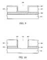
- FIGS. 9-11Bare cross sections of showing a method of fabricating a phase-change according to another embodiment of the invention.
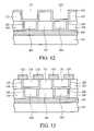
- FIGS. 12-15are cross sections of showing a method of fabricating a three-demensional phase-change memory according to yet another embodiment of the invention.
- a substrate 101is provided, wherein the substrate 101 can be a semiconductor substrate.
- a bottom electrode 103is formed on the substrate 101 , wherein the bottom electrode 103 can be TiN, TaN, or TiW, and formed by CVD or sputtering.
- an isolation layer 105is formed on the bottom electrode 103 .
- the isolation layer 105is preferably thicker than the bottom electrode 103 .
- the material of the isolation layer 105may be borophosphosilicate glass (BPSG), silicon oxide, or silicon nitride, serving as the etching-stop of a subsequent chemical mechanical polishing (CMP) process.
- BPSGborophosphosilicate glass
- CMPchemical mechanical polishing
- the isolation layeris patterned by photolithography processes to form a plurality of trenches 201 exposing the bottom electrode 103 .
- the distance between the phase-change materials of memories of the inventiondepends on the width of the trenches 201 .
- the trench 201extends in a first extension direction.
- phase-change material 203is conformably formed on the isolation layer 105 and the bottom electrode 103 , completely covering the sidewalls and the bottom of the trenches 201 , wherein the phase-change material 203 covers the top surface of the bottom electrode 103 within the trenches 201 .
- the phase-change material 203can be a chalcogenide material or comprise In, Ge, Sb, Te or combinations thereof, such as GeSbTe or InGeSbTe.
- the thickness of the phase-change material 203can be 20 nm to 100 nm, preferably 50 nm.
- an isolation material 305is filled into the trenches 201 and planarized by a planarization process, such as CMP, leaving coplanar top surfaces of the isolation layer 105 , phase-change material 203 , and isolation layer 305 .
- a planarization processsuch as CMP
- the material of the isolation layer 305can be borophosphosilicate glass (BPSG), silicon oxide, or silicon nitride.
- BPSGborophosphosilicate glass
- silicon oxidesilicon oxide
- silicon nitridesilicon nitride
- the material of the isolation layer 305 and the isolation layer 105is substantially the same.
- the etching back processmay replace the planarization process.
- a photoresist layeris formed on the isolation layer 105 , phase-change material 203 , and isolation layer 305 and patterned to form a plurality of photoresist patterns 401 extending in a second extension direction parallel to the first direction.
- the photoresist patterns 401cover the entire top surface of the phase-change material 203 and partially cover the top surface of the isolation layer 305 and isolation layer 105 .
- the distance between the memoriesdepends on the distance between the photoresist patterns 401 .
- the isolation layer 105 , isolation layer 305 , phase-change material 203 , and bottom electrode 103are etched with the photoresist patterns as a mask exposing the substrate 101 , completing the structure 501 as shown in FIG. 5 .
- the phase-change material 203is formed between the isolation layer 105 and isolation layer 305 and is L-shaped or ⁇ -shaped and electrically connects to the bottom electrode 103 .
- an isolation layer 605is filled into the openings between the stacked structures 501 .
- the material of the isolation layer 605can be borophosphosilicate glass (BPSG), silicon oxide, or silicon nitride.
- the material of the isolation layer 605 and the isolation layer 105is substantially the same.
- the isolation layer 105 , phase-change material 203 , isolation layer 305 , and isolation layer 605are planarized by a planarization process, such as chemical mechanical polishing, resulting in coplanar top surfaces of the isolation layer 105 , phase-change material 203 , isolation layer 305 , and isolation layer 605 .
- a photoresist layeris formed on the isolation layer 105 , phase-change material 203 , isolation layer 305 and isolation layer 605 , and patterned to form a plurality of photoresist patterns 601 extending in a third extension direction perpendicular to the first direction.
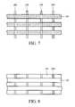
- FIG. 7shows the top-view of FIG. 6 .
- the width W of the photoresist patterns 601is preferably the same as the resolution limit of photolithography process, resulting in reducing the top area of the phase-change material and increasing the current density of the phase-change memory.
- isolation layer 105 , isolation layer 305 , isolation layer 605 , phase-change material 203 , and bottom electrode 103are etched with the photoresist patterns 601 as a mask exposing the substrate 101 .
- FIG. 8shows the top-view of the described structure.
- the order of forming the photoresist patterns 401 and the photoresist patterns 601can be changed. Referring to FIG. 3 , after performing the first planarization, the photoresist patterns extending in a extension direction perpendicular to the first direction can be formed on the isolation layer 105 , phase-change material 203 , and isolation layer 305 . After etching and deposition of the isolation, the photoresist patterns extending in a extension direction parallel to the first direction are then formed.
- a method of fabricating a phase-change memoryis also provided. Referring to FIG. 9 , a conducting layer 903 and an isolation layer 905 are formed on a substrate 901 .
- Suitable materials for the conducting layer 903can be TiN, TaN, or TiW, serving as the bottom electrode of the invention.
- the material of the isolation layer 905may be borophosphosilicate glass (BPSG), silicon oxide, or silicon nitride.
- BPSGborophosphosilicate glass
- the isolation layer 905is patterned to form a plurality of trenches 909 exposing the conducting layer 903
- phase-change material 907is conformably formed on the isolation layer 905 and the conducting layer 903 , completely covering the sidewalls and the bottom of the trenches 909 , wherein the phase-change material 907 cover the top surface of the conducting layer 903 within the trenches 909 .
- the phase-change material 907can be chalcogenide material or comprise In, Ge, Sb, Te or combinations thereof, such as GeSbTe or InGeSbTe.
- the thickness of the phase-change material 907can be 20 nm to 100 nm, preferably 50 nm.
- the phase-change material 907is etched by an anisotropic etching to remain a phase-change material pillar adjacent to the sidewalls of the trenches.
- the conducting layer 903 within the trenches 909is etched to form openings 910 exposing the substrate 901 .
- an isolation layer 911is formed to fill the openings 910 , and planarized by a planarization process, such as chemical mechanical polishing, leaving coplanar top surfaces of the isolation layer 905 , phase-change material 907 , and isolation layer 911 .
- the material of the isolation layer 911may be borophosphosilicate glass (BPSG), silicon oxide, or silicon nitride.
- BPSGborophosphosilicate glass
- FIG. 11Bthe described structure is subjected to the process as disclosed in FIGS. 6 ⁇ 8 , thus, fabrication of the phase-change memory is complete.
- the phase-change material pillaris formed between the isolation layer 905 , and isolation layer 911 , and the profile of the phase-change material pillar is I-shaped.
- the method for fabricating a three-dimensional phase-change memorycomprises: after planarization process as disclosed in FIG. 3 , an isolation layer 121 is formed on the isolation layer 105 , phase-change material 203 , and isolation layer 305 .
- the material of the isolation layer 121can be borophosphosilicate glass (BPSG), silicon oxide, or silicon nitride.
- the isolation layer 121is patterned to form a plurality of trenches 123 , wherein the trenches 123 are parallel to and directly over the trenches 201 .
- the width of the trenches 123can be the same as the trenches 201 , and the trenches 123 and trench 201 extend to a first extension direction.
- a phase-change material 125is formed conformably on the isolation layer 121 and the trenches 123 , wherein the phase-change material 125 cover the sidewalls and the bottom of the trenches 125 .
- An isolation layer 131is filled into the trenches 123 .
- the material of the isolation layer 131can be borophosphosilicate glass (BPSG), silicon oxide, or silicon nitride.
- the isolation layer 121 , phase-change material 125 , and isolation layer 131are planarized by a planarization process, such as chemical mechanical polishing, leaving coplanar top surfaces of the isolation layer 121 , phase-change material 125 , and isolation layer 131 .
- the etching back processmay replace the planarization process.
- a photoresist layeris formed on the isolation layer 121 , phase-change material 125 , and isolation layer 131 , and patterned to form a plurality of photoresist patterns 133 extending in a second extension direction parallel to the first extension direction.
- the photoresist patterns 133cover the entire top surface of the phase-change material 203 and phase-change material 125 adjacent to the sidewalls of the trenches 201 and trenches 123 and cover a partial top surface of the isolation layer 131 and isolation layer 121 .
- the isolation layer 121 , isolation layer 131 , phase-change material 203 , phase-change material 125 , isolation layer 105 , isolation layer 301 and bottom electrode 103are etched with the photoresist patterns 133 as a mask exposing the substrate 101 , forming a plurality of stacked structures 141 .
- the phase-change material 125is formed between the isolation layer 131 and isolation layer 121
- phase-change material 203is formed between the isolation layer 301 and isolation layer 105 .
- the phase-change material 125 and phase-change material 203are L-shaped or ⁇ -shaped, electrically connecting each other.
- phase-change material 125 and phase-change material 203can be formed between the phase-change material 125 and phase-change material 203 , serving as an electrode.
- a conducting layersuch as TiN, TaN, or TiW, can be formed between the phase-change material 125 and phase-change material 203 , serving as an electrode.
- datacan be read in logic “10”, logic “01”, logic “00”, or logic “11” by detecting current flowing through the phase-change memory when a predetermined voltage applied, thereby increasing the memory density thereof.
- an isolation layer 151is formed on the substrate to fill the space between the stacked structures 141 , and planarized by a planarization process, such as chemical mechanical polishing, leaving coplanar top surfaces of the isolation layer 121 , isolation layer 131 , isolation layer 151 , and isolation layer 125 .
- the material of the isolation layer 151can be borophosphosilicate glass (BPSG), silicon oxide, or silicon nitride.
- a photoresist layeris formed on the above structure to form a plurality of photoresist patterns 153 extending in a third extension direction perpendicular to the first direction.
- the top-view of the aforementioned structureis the same as the FIG. 7 .
- the width of the photoresist patterns 153is preferably the same as the resolution limit of photolithography process, resulting in reducing the top area of the phase-change material and increasing the current density of the phase-change memory.
- isolation layer 121 , isolation layer 131 , isolation layer 105 , isolation layer 301 , phase-change material 125 , phase-change material 203 , and bottom electrode 103are etched with the photoresist patterns 153 as a mask exposing the substrate 101 .
- FIG. 8shows the top-view of the above structure.
- a conducting layeris formed on the top surface of the phase-change material 125 for electrical connection thereto.
- the conducting layeris etched to form a plurality of top electrodes extending in a fourth extension direction perpendicular to the first extension direction.
- the contact area between the phase-change material and top electrodedepends on the deposition thickness of the phase-change material and the width of the photoresist patterns. Therefore, the phase-change material can have a diameter less than the resolution limit of the photolithography process. As a result, an operating current for a state conversion of the phase-change material pattern may be reduced so as to decrease a power dissipation of the phase-change memory device. In addition, because the operating current decreases, sizes of other discrete devices (e.g., MOS transistor) of the phase-change memory device may also be decreased. Therefore, the phase-change memory device may be suitable for high integration.
- the phase-change memorieshave four kinds of logic single, thereby increasing the memory density thereof.
Landscapes
- Engineering & Computer Science (AREA)
- Manufacturing & Machinery (AREA)
- Semiconductor Memories (AREA)
Abstract
Description
- 1. Field of the Invention
- The invention relates to a memory, and more particularly to a phase-change memory.
- 2. Description of the Related Art
- Phase change memories are non-volatile, have high density, high contrast, high cycling, and low power-consumption, thus, they are an industry semiconductor of choice. Particularly, a phase-change memory with high cell density capable of changing memory states with low current is desirable.
- Phase-change materials may exhibit at least two different states, comprising amorphous and crystalline states. Phase-change materials may change from the amorphous to the crystalline state, and back, in response to temperature changes. The states may be distinguished because the amorphous state generally exhibits higher resistivity than the crystalline state. The amorphous state typically involves a more disordered atomic structure, while the crystalline state is an ordered lattice. In general, chalcogenide materials have been widely used in various optical recording media.
- The resistance of the phase-change material varies according to whether the phase-change material is in a crystalline state or an amorphous state. In detail, the phase-change material exhibits greater resistance when it is in an amorphous state than when it is in a crystalline state. Therefore, data can be read as logic “0” or logic “1” by detecting current flowing through the phase-change memory when a predetermined voltage applied. That is, data can be stored in a digital form, logic “0” or logic “1”, without accumulation of electric charge.
- U.S. Pat. No. 6,031,287 and U.S. Pat. No. 6,797,978 disclose horizontal phase-change memory with reduced phase-change material contact area and sufficient current density.
- In one embodiment of the invention, the phase-change memory comprises a bottom electrode formed on a substrate. A first isolation layer is formed on the bottom electrode. A top electrode is formed on the isolation layer. A first phase-change material is formed in the first isolation layer, wherein the top electrode and the bottom electrode are electrically connected via the first phase-change material. Since the phase-change material can have a diameter less than the resolution limit of the photolithography process, an operating current for a state conversion of the phase-change material pattern may be reduced so as to decrease a power dissipation of the phase-change memory device.
- Methods of manufacturing phase-change memories are also provided. An exemplary embodiment of a method comprises the following steps: forming a bottom electrode on a substrate; forming a first isolation layer on the bottom electrode, wherein the first isolation layer comprises a plurality of first trenches exposing the bottom electrode, and the first trenches extend in a first extension direction; conformably forming a first phase-change material on the first isolation layer and the substrate, wherein the first phase-change material covers the surface of the first trenches; forming a second isolation layer to fill the first trenches; subjecting the first isolation layer, the first phase-change material, and the second isolation layer to a planarization process; forming a plurality of first photoresist patterns extending in an second extension direction parallel to the first extension direction, wherein the first photoresist patterns cover the top surface of the first phase-change material and exposing the top surface of the second isolation layer formed into the first trenches; and etching the first isolation layer, second isolation layer, first phase-change material, and bottom electrode with the first photoresist patterns as a mask exposing the substrate.
- According to another exemplary embodiment of the invention, the method of manufacturing phase-change memory comprises the following steps: forming a bottom electrode on a substrate; forming a first isolation layer on the bottom electrode; patterning the first isolation layer so as to form a trench exposing the bottom electrode; conformably forming a phase-change material to cover the surface of the first isolation layer and the trench; etching the phase-change material to leave a phase-change material pillar adjacent to the sidewalls of the trenches; etching the bottom electrode exposed in the trenches to expose the substrate; and forming a second isolation layer to fill the trench.
- A detailed description is given in the following embodiments with reference to the accompanying drawings.
- The invention can be more fully understood by reading the subsequent detailed description and examples with references made to the accompanying drawings, wherein:
FIGS. 1-8 are cross sections of showing a method of fabricating a phase-change memory according to an embodiment of the invention.FIGS. 9-11B are cross sections of showing a method of fabricating a phase-change according to another embodiment of the invention.FIGS. 12-15 are cross sections of showing a method of fabricating a three-demensional phase-change memory according to yet another embodiment of the invention.- The following description is the best-contemplated mode of carrying out the invention. This description is made for the purpose of illustrating the general principles of the invention and should not be taken in a limiting sense. The scope of the invention is best determined by reference to the appended claims.
- Referring to
FIG. 1 , asubstrate 101 is provided, wherein thesubstrate 101 can be a semiconductor substrate. Next, abottom electrode 103 is formed on thesubstrate 101, wherein thebottom electrode 103 can be TiN, TaN, or TiW, and formed by CVD or sputtering. Next, anisolation layer 105 is formed on thebottom electrode 103. Theisolation layer 105 is preferably thicker than thebottom electrode 103. For example, the material of theisolation layer 105 may be borophosphosilicate glass (BPSG), silicon oxide, or silicon nitride, serving as the etching-stop of a subsequent chemical mechanical polishing (CMP) process. - Next, referring to
FIG. 2 , the isolation layer is patterned by photolithography processes to form a plurality oftrenches 201 exposing thebottom electrode 103. Note that the distance between the phase-change materials of memories of the invention depends on the width of thetrenches 201. Thetrench 201 extends in a first extension direction. - Next, a phase-
change material 203 is conformably formed on theisolation layer 105 and thebottom electrode 103, completely covering the sidewalls and the bottom of thetrenches 201, wherein the phase-change material 203 covers the top surface of thebottom electrode 103 within thetrenches 201. The phase-change material 203 can be a chalcogenide material or comprise In, Ge, Sb, Te or combinations thereof, such as GeSbTe or InGeSbTe. Particularly, the thickness of the phase-change material 203 can be 20 nm to 100 nm, preferably 50 nm. - Referring to
FIG. 3 , anisolation material 305 is filled into thetrenches 201 and planarized by a planarization process, such as CMP, leaving coplanar top surfaces of theisolation layer 105, phase-change material 203, andisolation layer 305. For example, the material of theisolation layer 305 can be borophosphosilicate glass (BPSG), silicon oxide, or silicon nitride. Preferably, the material of theisolation layer 305 and theisolation layer 105 is substantially the same. The etching back process may replace the planarization process. - Next, referring to
FIG. 4 , a photoresist layer is formed on theisolation layer 105, phase-change material 203, andisolation layer 305 and patterned to form a plurality ofphotoresist patterns 401 extending in a second extension direction parallel to the first direction. Thephotoresist patterns 401 cover the entire top surface of the phase-change material 203 and partially cover the top surface of theisolation layer 305 andisolation layer 105. The distance between the memories depends on the distance between thephotoresist patterns 401. - The
isolation layer 105,isolation layer 305, phase-change material 203, andbottom electrode 103 are etched with the photoresist patterns as a mask exposing thesubstrate 101, completing thestructure 501 as shown inFIG. 5 . It should be noted that the phase-change material 203 is formed between theisolation layer 105 andisolation layer 305 and is L-shaped or ┘-shaped and electrically connects to thebottom electrode 103. - Referring to
FIG. 6 , anisolation layer 605 is filled into the openings between thestacked structures 501. For example, the material of theisolation layer 605 can be borophosphosilicate glass (BPSG), silicon oxide, or silicon nitride. Preferably, the material of theisolation layer 605 and theisolation layer 105 is substantially the same. Theisolation layer 105, phase-change material 203,isolation layer 305, andisolation layer 605 are planarized by a planarization process, such as chemical mechanical polishing, resulting in coplanar top surfaces of theisolation layer 105, phase-change material 203,isolation layer 305, andisolation layer 605. - Still referring to
FIG. 6 , a photoresist layer is formed on theisolation layer 105, phase-change material 203,isolation layer 305 andisolation layer 605, and patterned to form a plurality ofphotoresist patterns 601 extending in a third extension direction perpendicular to the first direction.FIG. 7 shows the top-view ofFIG. 6 . The width W of thephotoresist patterns 601 is preferably the same as the resolution limit of photolithography process, resulting in reducing the top area of the phase-change material and increasing the current density of the phase-change memory. - The
isolation layer 105,isolation layer 305,isolation layer 605, phase-change material 203, andbottom electrode 103 are etched with thephotoresist patterns 601 as a mask exposing thesubstrate 101.FIG. 8 shows the top-view of the described structure. - In another embodiment, the order of forming the
photoresist patterns 401 and thephotoresist patterns 601 can be changed. Referring toFIG. 3 , after performing the first planarization, the photoresist patterns extending in a extension direction perpendicular to the first direction can be formed on theisolation layer 105, phase-change material 203, andisolation layer 305. After etching and deposition of the isolation, the photoresist patterns extending in a extension direction parallel to the first direction are then formed. - A method of fabricating a phase-change memory is also provided. Referring to
FIG. 9 , aconducting layer 903 and anisolation layer 905 are formed on asubstrate 901. - Suitable materials for the
conducting layer 903 can be TiN, TaN, or TiW, serving as the bottom electrode of the invention. For example, the material of theisolation layer 905 may be borophosphosilicate glass (BPSG), silicon oxide, or silicon nitride. Next, theisolation layer 905 is patterned to form a plurality oftrenches 909 exposing theconducting layer 903 - A phase-
change material 907 is conformably formed on theisolation layer 905 and theconducting layer 903, completely covering the sidewalls and the bottom of thetrenches 909, wherein the phase-change material 907 cover the top surface of theconducting layer 903 within thetrenches 909. The phase-change material 907 can be chalcogenide material or comprise In, Ge, Sb, Te or combinations thereof, such as GeSbTe or InGeSbTe. Particularly, the thickness of the phase-change material 907 can be 20 nm to 100 nm, preferably 50 nm. - Referring to
FIG. 10 , the phase-change material 907 is etched by an anisotropic etching to remain a phase-change material pillar adjacent to the sidewalls of the trenches. Next, theconducting layer 903 within thetrenches 909 is etched to formopenings 910 exposing thesubstrate 901. - Next, referring to
FIG. 11A , anisolation layer 911 is formed to fill theopenings 910, and planarized by a planarization process, such as chemical mechanical polishing, leaving coplanar top surfaces of theisolation layer 905, phase-change material 907, andisolation layer 911. For example, the material of theisolation layer 911 may be borophosphosilicate glass (BPSG), silicon oxide, or silicon nitride. Referring toFIG. 11B , the described structure is subjected to the process as disclosed inFIGS. 6˜8 , thus, fabrication of the phase-change memory is complete. Particularly, the phase-change material pillar is formed between theisolation layer 905, andisolation layer 911, and the profile of the phase-change material pillar is I-shaped. - In some embodiments of the method for fabricating a three-dimensional phase-change memory comprises: after planarization process as disclosed in
FIG. 3 , anisolation layer 121 is formed on theisolation layer 105, phase-change material 203, andisolation layer 305. For example, the material of theisolation layer 121 can be borophosphosilicate glass (BPSG), silicon oxide, or silicon nitride. Next, theisolation layer 121 is patterned to form a plurality oftrenches 123, wherein thetrenches 123 are parallel to and directly over thetrenches 201. Particularly, the width of thetrenches 123 can be the same as thetrenches 201, and thetrenches 123 andtrench 201 extend to a first extension direction. - A phase-
change material 125 is formed conformably on theisolation layer 121 and thetrenches 123, wherein the phase-change material 125 cover the sidewalls and the bottom of thetrenches 125. Anisolation layer 131 is filled into thetrenches 123. For example, the material of theisolation layer 131 can be borophosphosilicate glass (BPSG), silicon oxide, or silicon nitride. - The
isolation layer 121, phase-change material 125, andisolation layer 131 are planarized by a planarization process, such as chemical mechanical polishing, leaving coplanar top surfaces of theisolation layer 121, phase-change material 125, andisolation layer 131. The etching back process may replace the planarization process. - Referring to
FIG. 13 , after planarization, a photoresist layer is formed on theisolation layer 121, phase-change material 125, andisolation layer 131, and patterned to form a plurality ofphotoresist patterns 133 extending in a second extension direction parallel to the first extension direction. - The
photoresist patterns 133 cover the entire top surface of the phase-change material 203 and phase-change material 125 adjacent to the sidewalls of thetrenches 201 andtrenches 123 and cover a partial top surface of theisolation layer 131 andisolation layer 121. - Next, referring to
FIG. 14 , theisolation layer 121,isolation layer 131, phase-change material 203, phase-change material 125,isolation layer 105, isolation layer301 andbottom electrode 103 are etched with thephotoresist patterns 133 as a mask exposing thesubstrate 101, forming a plurality ofstacked structures 141. The phase-change material 125 is formed between theisolation layer 131 andisolation layer 121, and phase-change material 203 is formed between the isolation layer301 andisolation layer 105. The phase-change material 125 and phase-change material 203 are L-shaped or ┘-shaped, electrically connecting each other. Further, a conducting layer (not shown), such as TiN, TaN, or TiW, can be formed between the phase-change material 125 and phase-change material 203, serving as an electrode. Preferably, since the phase-change material 125 and phase-change material 203 comprise different materials, data can be read in logic “10”, logic “01”, logic “00”, or logic “11” by detecting current flowing through the phase-change memory when a predetermined voltage applied, thereby increasing the memory density thereof. - Next, referring to
FIG. 15 , anisolation layer 151 is formed on the substrate to fill the space between thestacked structures 141, and planarized by a planarization process, such as chemical mechanical polishing, leaving coplanar top surfaces of theisolation layer 121,isolation layer 131,isolation layer 151, andisolation layer 125. For example, the material of theisolation layer 151 can be borophosphosilicate glass (BPSG), silicon oxide, or silicon nitride. - Next, a photoresist layer is formed on the above structure to form a plurality of
photoresist patterns 153 extending in a third extension direction perpendicular to the first direction. The top-view of the aforementioned structure is the same as theFIG. 7 . - The width of the
photoresist patterns 153 is preferably the same as the resolution limit of photolithography process, resulting in reducing the top area of the phase-change material and increasing the current density of the phase-change memory. - The
isolation layer 121,isolation layer 131,isolation layer 105, isolation layer301, phase-change material 125, phase-change material 203, andbottom electrode 103 are etched with thephotoresist patterns 153 as a mask exposing thesubstrate 101.FIG. 8 shows the top-view of the above structure. - After removing the
photoresist patterns 153, a conducting layer is formed on the top surface of the phase-change material 125 for electrical connection thereto. Next, the conducting layer is etched to form a plurality of top electrodes extending in a fourth extension direction perpendicular to the first extension direction. - Accordingly, the contact area between the phase-change material and top electrode depends on the deposition thickness of the phase-change material and the width of the photoresist patterns. Therefore, the phase-change material can have a diameter less than the resolution limit of the photolithography process. As a result, an operating current for a state conversion of the phase-change material pattern may be reduced so as to decrease a power dissipation of the phase-change memory device. In addition, because the operating current decreases, sizes of other discrete devices (e.g., MOS transistor) of the phase-change memory device may also be decreased. Therefore, the phase-change memory device may be suitable for high integration.
- Moreover, in an embodiment of the invention, the phase-change memories have four kinds of logic single, thereby increasing the memory density thereof.
- While the invention has been described by way of example and in terms of preferred embodiment, it is to be understood that the invention is not limited thereto. To the contrary, it is intended to cover various modifications and similar arrangements (as would be apparent to those skilled in the art). Therefore, the scope of the appended claims should be accorded the broadest interpretation so as to encompass all such modifications and similar arrangements.
Claims (30)
Priority Applications (2)
| Application Number | Priority Date | Filing Date | Title |
|---|---|---|---|
| US12/187,345US7670871B2 (en) | 2006-08-14 | 2008-08-06 | Method of fabricating a phase-change memory |
| US12/611,066US7923286B2 (en) | 2006-08-14 | 2009-11-02 | Method of fabricating a phase-change memory |
Applications Claiming Priority (2)
| Application Number | Priority Date | Filing Date | Title |
|---|---|---|---|
| TW095129774ATWI305678B (en) | 2006-08-14 | 2006-08-14 | Phase-change memory and fabricating method thereof |
| TWTW95129774 | 2006-08-14 |
Related Child Applications (1)
| Application Number | Title | Priority Date | Filing Date |
|---|---|---|---|
| US12/187,345DivisionUS7670871B2 (en) | 2006-08-14 | 2008-08-06 | Method of fabricating a phase-change memory |
Publications (2)
| Publication Number | Publication Date |
|---|---|
| US20080035961A1true US20080035961A1 (en) | 2008-02-14 |
| US7569845B2 US7569845B2 (en) | 2009-08-04 |
Family
ID=39049831
Family Applications (3)
| Application Number | Title | Priority Date | Filing Date |
|---|---|---|---|
| US11/552,492Active2027-03-08US7569845B2 (en) | 2006-08-14 | 2006-10-24 | Phase-change memory and fabrication method thereof |
| US12/187,345ActiveUS7670871B2 (en) | 2006-08-14 | 2008-08-06 | Method of fabricating a phase-change memory |
| US12/611,066ActiveUS7923286B2 (en) | 2006-08-14 | 2009-11-02 | Method of fabricating a phase-change memory |
Family Applications After (2)
| Application Number | Title | Priority Date | Filing Date |
|---|---|---|---|
| US12/187,345ActiveUS7670871B2 (en) | 2006-08-14 | 2008-08-06 | Method of fabricating a phase-change memory |
| US12/611,066ActiveUS7923286B2 (en) | 2006-08-14 | 2009-11-02 | Method of fabricating a phase-change memory |
Country Status (2)
| Country | Link |
|---|---|
| US (3) | US7569845B2 (en) |
| TW (1) | TWI305678B (en) |
Cited By (32)
| Publication number | Priority date | Publication date | Assignee | Title |
|---|---|---|---|---|
| US20090087561A1 (en)* | 2007-09-28 | 2009-04-02 | Advanced Technology Materials, Inc. | Metal and metalloid silylamides, ketimates, tetraalkylguanidinates and dianionic guanidinates useful for cvd/ald of thin films |
| US20090124039A1 (en)* | 2006-05-12 | 2009-05-14 | Advanced Technology Materials, Inc. | Low temperature deposition of phase change memory materials |
| US20090196091A1 (en)* | 2008-01-31 | 2009-08-06 | Kau Derchang | Self-aligned phase change memory |
| US20090215225A1 (en)* | 2008-02-24 | 2009-08-27 | Advanced Technology Materials, Inc. | Tellurium compounds useful for deposition of tellurium containing materials |
| US20100051896A1 (en)* | 2008-09-02 | 2010-03-04 | Samsung Electronics Co., Ltd. | Variable resistance memory device using a channel-shaped variable resistance pattern |
| US20100112774A1 (en)* | 2008-10-30 | 2010-05-06 | Gyuhwan Oh | Variable Resistance Memory Device and Methods of Forming the Same |
| US20100176365A1 (en)* | 2009-01-09 | 2010-07-15 | Samsung Electronics Co., Ltd. | Resistance variable memory devices and methods of fabricating the same |
| US20100279011A1 (en)* | 2007-10-31 | 2010-11-04 | Advanced Technology Materials, Inc. | Novel bismuth precursors for cvd/ald of thin films |
| US20110001107A1 (en)* | 2009-07-02 | 2011-01-06 | Advanced Technology Materials, Inc. | Hollow gst structure with dielectric fill |
| US20110111556A1 (en)* | 2008-05-02 | 2011-05-12 | Advanced Technology Materials, Inc. | Antimony compounds useful for deposition of antimony-containing materials |
| US20110124182A1 (en)* | 2009-11-20 | 2011-05-26 | Advanced Techology Materials, Inc. | System for the delivery of germanium-based precursor |
| US20110147692A1 (en)* | 2009-12-21 | 2011-06-23 | Jeonghee Park | Variable resistance memory device and method of forming the same |
| US20110180905A1 (en)* | 2008-06-10 | 2011-07-28 | Advanced Technology Materials, Inc. | GeSbTe MATERIAL INCLUDING SUPERFLOW LAYER(S), AND USE OF Ge TO PREVENT INTERACTION OF Te FROM SbXTeY AND GeXTeY RESULTING IN HIGH Te CONTENT AND FILM CRYSTALLINITY |
| WO2011119895A3 (en)* | 2010-03-24 | 2011-12-22 | Advanced Technology Materials, Inc. | Method for forming phase change memory device |
| WO2011149505A3 (en)* | 2010-05-25 | 2012-02-02 | Micron Technology, Inc. | Resistance variable memory cell structures and methods |
| US8268665B2 (en) | 2006-11-02 | 2012-09-18 | Advanced Technology Materials, Inc. | Antimony and germanium complexes useful for CVD/ALD of metal thin films |
| US8330136B2 (en) | 2008-12-05 | 2012-12-11 | Advanced Technology Materials, Inc. | High concentration nitrogen-containing germanium telluride based memory devices and processes of making |
| US20130105756A1 (en)* | 2011-10-26 | 2013-05-02 | Samsung Electronics Co., Ltd. | Phase-change memory device |
| US8507353B2 (en) | 2010-08-11 | 2013-08-13 | Samsung Electronics Co., Ltd. | Method of forming semiconductor device having self-aligned plug |
| US8617972B2 (en) | 2009-05-22 | 2013-12-31 | Advanced Technology Materials, Inc. | Low temperature GST process |
| US8686394B2 (en) | 2012-07-18 | 2014-04-01 | Micron Technology, Inc. | Semiconductor constructions and memory arrays |
| CN103811656A (en)* | 2012-11-09 | 2014-05-21 | 台湾积体电路制造股份有限公司 | Resistance variable memory structure and forming method thereof |
| US20140256110A1 (en)* | 2010-05-12 | 2014-09-11 | International Business Machines Corporation | Self aligned fin-type programmable memory cell |
| US8834968B2 (en) | 2007-10-11 | 2014-09-16 | Samsung Electronics Co., Ltd. | Method of forming phase change material layer using Ge(II) source, and method of fabricating phase change memory device |
| US8853665B2 (en) | 2012-07-18 | 2014-10-07 | Micron Technology, Inc. | Semiconductor constructions, memory cells, memory arrays and methods of forming memory cells |
| US8852686B2 (en) | 2007-10-11 | 2014-10-07 | Samsung Electronics Co., Ltd. | Method of forming phase change material layer using Ge(II) source, and method of fabricating phase change memory device |
| US9012876B2 (en) | 2010-03-26 | 2015-04-21 | Entegris, Inc. | Germanium antimony telluride materials and devices incorporating same |
| US9166159B2 (en) | 2013-05-23 | 2015-10-20 | Micron Technology, Inc. | Semiconductor constructions and methods of forming memory cells |
| US9190609B2 (en) | 2010-05-21 | 2015-11-17 | Entegris, Inc. | Germanium antimony telluride materials and devices incorporating same |
| US9640757B2 (en) | 2012-10-30 | 2017-05-02 | Entegris, Inc. | Double self-aligned phase change memory device structure |
| US11177436B2 (en)* | 2019-04-25 | 2021-11-16 | International Business Machines Corporation | Resistive memory with embedded metal oxide fin for gradual switching |
| WO2024037524A1 (en)* | 2022-08-18 | 2024-02-22 | International Business Machines Corporation | Vertical phase change memory device |
Families Citing this family (12)
| Publication number | Priority date | Publication date | Assignee | Title |
|---|---|---|---|---|
| DE102008032067A1 (en)* | 2007-07-12 | 2009-01-15 | Samsung Electronics Co., Ltd., Suwon | Method for forming phase change memories with lower electrodes |
| US7939911B2 (en)* | 2008-08-14 | 2011-05-10 | International Business Machines Corporation | Back-end-of-line resistive semiconductor structures |
| US7977201B2 (en)* | 2008-08-14 | 2011-07-12 | International Business Machines Corporation | Methods for forming back-end-of-line resistive semiconductor structures |
| KR20130073038A (en)* | 2010-10-29 | 2013-07-02 | 휴렛-팩커드 디벨롭먼트 컴퍼니, 엘.피. | Memristive devices and memristors with ribbon-like junctions and methods for fabricating the same |
| US20130058158A1 (en) | 2011-09-01 | 2013-03-07 | Micron Technology, Inc. | Method, system, and device for l-shaped memory component |
| US8599599B2 (en) | 2011-09-01 | 2013-12-03 | Micron Technology, Inc. | Method, system, and device for phase change memory switch wall cell with approximately horizontal electrode contact |
| KR20130043533A (en)* | 2011-10-20 | 2013-04-30 | 삼성전자주식회사 | Non-volatile memory device having conductive buffer pattern and method of forming the same |
| US8962384B2 (en)* | 2012-01-20 | 2015-02-24 | Micron Technology, Inc. | Memory cells having heaters with angled sidewalls |
| US8981330B2 (en) | 2012-07-16 | 2015-03-17 | Macronix International Co., Ltd. | Thermally-confined spacer PCM cells |
| US10424619B2 (en) | 2016-01-13 | 2019-09-24 | Samsung Electronics Co., Ltd. | Variable resistance memory devices and methods of manufacturing the same |
| KR102475041B1 (en)* | 2016-02-22 | 2022-12-07 | 삼성전자주식회사 | Variable resistance memory devices and methods of manufacturing the same |
| KR102820467B1 (en) | 2020-09-15 | 2025-06-16 | 삼성전자주식회사 | Semiconductor device including data stroage material pattern |
Citations (11)
| Publication number | Priority date | Publication date | Assignee | Title |
|---|---|---|---|---|
| US5751012A (en)* | 1995-06-07 | 1998-05-12 | Micron Technology, Inc. | Polysilicon pillar diode for use in a non-volatile memory cell |
| US6002140A (en)* | 1995-06-07 | 1999-12-14 | Micron Technology, Inc. | Method for fabricating an array of ultra-small pores for chalcogenide memory cells |
| US6031287A (en)* | 1997-06-18 | 2000-02-29 | Micron Technology, Inc. | Contact structure and memory element incorporating the same |
| US20060030108A1 (en)* | 2004-08-04 | 2006-02-09 | Sung-Lae Cho | Semiconductor device and method of fabricating the same |
| US20060197130A1 (en)* | 2005-02-18 | 2006-09-07 | Suh Dong-Seok | Phase change memory devices and fabrication methods thereof |
| US20060226411A1 (en)* | 2005-04-06 | 2006-10-12 | Samsung Electronics Co., Ltd. | Multi-bit memory device having resistive material layers as storage node and methods of manufacturing and operating the same |
| US20060266993A1 (en)* | 2005-05-31 | 2006-11-30 | Samsung Electronics Co., Ltd. | Phase change random access memory devices and methods of operating the same |
| US20060284159A1 (en)* | 2005-06-10 | 2006-12-21 | Chang Heon Y | Phase change memory device and method for manufacturing the same |
| US20070048945A1 (en)* | 1999-03-25 | 2007-03-01 | Wolodymyr Czubatyj | Memory device and method of making same |
| US20070069249A1 (en)* | 2005-09-12 | 2007-03-29 | Elpida Memory Inc. | Phase change memory device and method of manufacturing the device |
| US20070075304A1 (en)* | 2005-09-30 | 2007-04-05 | Chang Heon Y | Reduced current phase-change memory device |
Family Cites Families (5)
| Publication number | Priority date | Publication date | Assignee | Title |
|---|---|---|---|---|
| US5952671A (en)* | 1997-05-09 | 1999-09-14 | Micron Technology, Inc. | Small electrode for a chalcogenide switching device and method for fabricating same |
| US7242019B2 (en)* | 2002-12-13 | 2007-07-10 | Intel Corporation | Shunted phase change memory |
| US7135696B2 (en)* | 2004-09-24 | 2006-11-14 | Intel Corporation | Phase change memory with damascene memory element |
| KR100585161B1 (en)* | 2004-10-02 | 2006-05-30 | 삼성전자주식회사 | Multichannel transistor device manufacturing method and device |
| US7220983B2 (en)* | 2004-12-09 | 2007-05-22 | Macronix International Co., Ltd. | Self-aligned small contact phase-change memory method and device |
- 2006
- 2006-08-14TWTW095129774Apatent/TWI305678B/enactive
- 2006-10-24USUS11/552,492patent/US7569845B2/enactiveActive
- 2008
- 2008-08-06USUS12/187,345patent/US7670871B2/enactiveActive
- 2009
- 2009-11-02USUS12/611,066patent/US7923286B2/enactiveActive
Patent Citations (12)
| Publication number | Priority date | Publication date | Assignee | Title |
|---|---|---|---|---|
| US5751012A (en)* | 1995-06-07 | 1998-05-12 | Micron Technology, Inc. | Polysilicon pillar diode for use in a non-volatile memory cell |
| US6002140A (en)* | 1995-06-07 | 1999-12-14 | Micron Technology, Inc. | Method for fabricating an array of ultra-small pores for chalcogenide memory cells |
| US6797978B2 (en)* | 1995-06-07 | 2004-09-28 | Micron Technology, Inc. | Method for fabricating an array of ultra-small pores for chalcogenide memory cells |
| US6031287A (en)* | 1997-06-18 | 2000-02-29 | Micron Technology, Inc. | Contact structure and memory element incorporating the same |
| US20070048945A1 (en)* | 1999-03-25 | 2007-03-01 | Wolodymyr Czubatyj | Memory device and method of making same |
| US20060030108A1 (en)* | 2004-08-04 | 2006-02-09 | Sung-Lae Cho | Semiconductor device and method of fabricating the same |
| US20060197130A1 (en)* | 2005-02-18 | 2006-09-07 | Suh Dong-Seok | Phase change memory devices and fabrication methods thereof |
| US20060226411A1 (en)* | 2005-04-06 | 2006-10-12 | Samsung Electronics Co., Ltd. | Multi-bit memory device having resistive material layers as storage node and methods of manufacturing and operating the same |
| US20060266993A1 (en)* | 2005-05-31 | 2006-11-30 | Samsung Electronics Co., Ltd. | Phase change random access memory devices and methods of operating the same |
| US20060284159A1 (en)* | 2005-06-10 | 2006-12-21 | Chang Heon Y | Phase change memory device and method for manufacturing the same |
| US20070069249A1 (en)* | 2005-09-12 | 2007-03-29 | Elpida Memory Inc. | Phase change memory device and method of manufacturing the device |
| US20070075304A1 (en)* | 2005-09-30 | 2007-04-05 | Chang Heon Y | Reduced current phase-change memory device |
Cited By (59)
| Publication number | Priority date | Publication date | Assignee | Title |
|---|---|---|---|---|
| US8679894B2 (en) | 2006-05-12 | 2014-03-25 | Advanced Technology Materials, Inc. | Low temperature deposition of phase change memory materials |
| US20090124039A1 (en)* | 2006-05-12 | 2009-05-14 | Advanced Technology Materials, Inc. | Low temperature deposition of phase change memory materials |
| US8288198B2 (en) | 2006-05-12 | 2012-10-16 | Advanced Technology Materials, Inc. | Low temperature deposition of phase change memory materials |
| US9219232B2 (en) | 2006-11-02 | 2015-12-22 | Entegris, Inc. | Antimony and germanium complexes useful for CVD/ALD of metal thin films |
| US8268665B2 (en) | 2006-11-02 | 2012-09-18 | Advanced Technology Materials, Inc. | Antimony and germanium complexes useful for CVD/ALD of metal thin films |
| US8709863B2 (en) | 2006-11-02 | 2014-04-29 | Advanced Technology Materials, Inc. | Antimony and germanium complexes useful for CVD/ALD of metal thin films |
| US20090087561A1 (en)* | 2007-09-28 | 2009-04-02 | Advanced Technology Materials, Inc. | Metal and metalloid silylamides, ketimates, tetraalkylguanidinates and dianionic guanidinates useful for cvd/ald of thin films |
| US8852686B2 (en) | 2007-10-11 | 2014-10-07 | Samsung Electronics Co., Ltd. | Method of forming phase change material layer using Ge(II) source, and method of fabricating phase change memory device |
| US8834968B2 (en) | 2007-10-11 | 2014-09-16 | Samsung Electronics Co., Ltd. | Method of forming phase change material layer using Ge(II) source, and method of fabricating phase change memory device |
| US20100279011A1 (en)* | 2007-10-31 | 2010-11-04 | Advanced Technology Materials, Inc. | Novel bismuth precursors for cvd/ald of thin films |
| US20090196091A1 (en)* | 2008-01-31 | 2009-08-06 | Kau Derchang | Self-aligned phase change memory |
| US8796068B2 (en) | 2008-02-24 | 2014-08-05 | Advanced Technology Materials, Inc. | Tellurium compounds useful for deposition of tellurium containing materials |
| US20090215225A1 (en)* | 2008-02-24 | 2009-08-27 | Advanced Technology Materials, Inc. | Tellurium compounds useful for deposition of tellurium containing materials |
| US9537095B2 (en) | 2008-02-24 | 2017-01-03 | Entegris, Inc. | Tellurium compounds useful for deposition of tellurium containing materials |
| US20110111556A1 (en)* | 2008-05-02 | 2011-05-12 | Advanced Technology Materials, Inc. | Antimony compounds useful for deposition of antimony-containing materials |
| US8674127B2 (en) | 2008-05-02 | 2014-03-18 | Advanced Technology Materials, Inc. | Antimony compounds useful for deposition of antimony-containing materials |
| US9034688B2 (en) | 2008-05-02 | 2015-05-19 | Entegris, Inc. | Antimony compounds useful for deposition of antimony-containing materials |
| US20110180905A1 (en)* | 2008-06-10 | 2011-07-28 | Advanced Technology Materials, Inc. | GeSbTe MATERIAL INCLUDING SUPERFLOW LAYER(S), AND USE OF Ge TO PREVENT INTERACTION OF Te FROM SbXTeY AND GeXTeY RESULTING IN HIGH Te CONTENT AND FILM CRYSTALLINITY |
| US20100051896A1 (en)* | 2008-09-02 | 2010-03-04 | Samsung Electronics Co., Ltd. | Variable resistance memory device using a channel-shaped variable resistance pattern |
| US20120305884A1 (en)* | 2008-10-30 | 2012-12-06 | Gyuhwan Oh | Variable resistance memory device and methods of forming the same |
| US8558348B2 (en)* | 2008-10-30 | 2013-10-15 | Samsung Electronics Co., Ltd. | Variable resistance memory device and methods of forming the same |
| US8278206B2 (en) | 2008-10-30 | 2012-10-02 | Samsung Electronics Co., Ltd. | Variable resistance memory device and methods of forming the same |
| US20100112774A1 (en)* | 2008-10-30 | 2010-05-06 | Gyuhwan Oh | Variable Resistance Memory Device and Methods of Forming the Same |
| US8330136B2 (en) | 2008-12-05 | 2012-12-11 | Advanced Technology Materials, Inc. | High concentration nitrogen-containing germanium telluride based memory devices and processes of making |
| US20100176365A1 (en)* | 2009-01-09 | 2010-07-15 | Samsung Electronics Co., Ltd. | Resistance variable memory devices and methods of fabricating the same |
| US9070875B2 (en) | 2009-05-22 | 2015-06-30 | Entegris, Inc. | Low temperature GST process |
| US8617972B2 (en) | 2009-05-22 | 2013-12-31 | Advanced Technology Materials, Inc. | Low temperature GST process |
| US20110001107A1 (en)* | 2009-07-02 | 2011-01-06 | Advanced Technology Materials, Inc. | Hollow gst structure with dielectric fill |
| US8410468B2 (en) | 2009-07-02 | 2013-04-02 | Advanced Technology Materials, Inc. | Hollow GST structure with dielectric fill |
| US20110124182A1 (en)* | 2009-11-20 | 2011-05-26 | Advanced Techology Materials, Inc. | System for the delivery of germanium-based precursor |
| US8552412B2 (en) | 2009-12-21 | 2013-10-08 | Samsung Electronics Co., Ltd. | Variable resistance memory device and method of forming the same |
| US8962438B2 (en) | 2009-12-21 | 2015-02-24 | Samsung Electronics Co., Ltd. | Variable resistance memory device and method of forming the same |
| US20110147692A1 (en)* | 2009-12-21 | 2011-06-23 | Jeonghee Park | Variable resistance memory device and method of forming the same |
| WO2011119895A3 (en)* | 2010-03-24 | 2011-12-22 | Advanced Technology Materials, Inc. | Method for forming phase change memory device |
| US9012876B2 (en) | 2010-03-26 | 2015-04-21 | Entegris, Inc. | Germanium antimony telluride materials and devices incorporating same |
| US20140256110A1 (en)* | 2010-05-12 | 2014-09-11 | International Business Machines Corporation | Self aligned fin-type programmable memory cell |
| US8853047B2 (en)* | 2010-05-12 | 2014-10-07 | Macronix International Co., Ltd. | Self aligned fin-type programmable memory cell |
| US9190609B2 (en) | 2010-05-21 | 2015-11-17 | Entegris, Inc. | Germanium antimony telluride materials and devices incorporating same |
| JP2013530525A (en)* | 2010-05-25 | 2013-07-25 | マイクロン テクノロジー, インク. | Resistance variable memory cell structure and method |
| CN102934229A (en)* | 2010-05-25 | 2013-02-13 | 美光科技公司 | Resistance variable memory cell structures and methods |
| TWI427743B (en)* | 2010-05-25 | 2014-02-21 | Micron Technology Inc | Resistance variable memory cell structures and methods |
| WO2011149505A3 (en)* | 2010-05-25 | 2012-02-02 | Micron Technology, Inc. | Resistance variable memory cell structures and methods |
| US8541765B2 (en) | 2010-05-25 | 2013-09-24 | Micron Technology, Inc. | Resistance variable memory cell structures and methods |
| KR101421367B1 (en)* | 2010-05-25 | 2014-07-18 | 마이크론 테크놀로지, 인크. | Resistance variable memory cell structures and methods |
| US9287502B2 (en) | 2010-05-25 | 2016-03-15 | Micron Technology, Inc. | Resistance variable memory cell structures and methods |
| US8790976B2 (en) | 2010-08-11 | 2014-07-29 | Samsung Electronics Co., Ltd. | Method of forming semiconductor device having self-aligned plug |
| US8507353B2 (en) | 2010-08-11 | 2013-08-13 | Samsung Electronics Co., Ltd. | Method of forming semiconductor device having self-aligned plug |
| US20130105756A1 (en)* | 2011-10-26 | 2013-05-02 | Samsung Electronics Co., Ltd. | Phase-change memory device |
| US8759143B1 (en) | 2012-07-18 | 2014-06-24 | Micron Technology, Inc. | Semiconductor constructions, memory arrays, methods of forming semiconductor constructions and methods of forming memory arrays |
| US8686394B2 (en) | 2012-07-18 | 2014-04-01 | Micron Technology, Inc. | Semiconductor constructions and memory arrays |
| US9245927B2 (en) | 2012-07-18 | 2016-01-26 | Micron Technology, Inc. | Semiconductor constructions, memory cells and memory arrays |
| US8853665B2 (en) | 2012-07-18 | 2014-10-07 | Micron Technology, Inc. | Semiconductor constructions, memory cells, memory arrays and methods of forming memory cells |
| US9640757B2 (en) | 2012-10-30 | 2017-05-02 | Entegris, Inc. | Double self-aligned phase change memory device structure |
| CN103811656A (en)* | 2012-11-09 | 2014-05-21 | 台湾积体电路制造股份有限公司 | Resistance variable memory structure and forming method thereof |
| US9166159B2 (en) | 2013-05-23 | 2015-10-20 | Micron Technology, Inc. | Semiconductor constructions and methods of forming memory cells |
| US9577188B2 (en) | 2013-05-23 | 2017-02-21 | Micron Technology, Inc. | Semiconductor constructions and methods of forming memory cells |
| US11177436B2 (en)* | 2019-04-25 | 2021-11-16 | International Business Machines Corporation | Resistive memory with embedded metal oxide fin for gradual switching |
| WO2024037524A1 (en)* | 2022-08-18 | 2024-02-22 | International Business Machines Corporation | Vertical phase change memory device |
| US12317762B2 (en) | 2022-08-18 | 2025-05-27 | International Business Machines Corporation | Vertical phase change memory device |
Also Published As
| Publication number | Publication date |
|---|---|
| US20100047960A1 (en) | 2010-02-25 |
| US20080311699A1 (en) | 2008-12-18 |
| US7569845B2 (en) | 2009-08-04 |
| US7670871B2 (en) | 2010-03-02 |
| US7923286B2 (en) | 2011-04-12 |
| TWI305678B (en) | 2009-01-21 |
| TW200810091A (en) | 2008-02-16 |
Similar Documents
| Publication | Publication Date | Title |
|---|---|---|
| US7670871B2 (en) | Method of fabricating a phase-change memory | |
| US8525298B2 (en) | Phase change memory device having 3 dimensional stack structure and fabrication method thereof | |
| CN100563040C (en) | Phase change memory cell and method of making same | |
| CN107093612B (en) | Variable resistance memory device and method of manufacturing the same | |
| JP5241717B2 (en) | Method for the controlled formation of a resistance switching material of a resistance switching device and the device obtained by the method | |
| CN101461071B (en) | A vertical phase change memory cell and methods for manufacturing thereof | |
| US7855378B2 (en) | Phase change memory devices and methods for fabricating the same | |
| US10573807B2 (en) | Phase change memory element | |
| KR100668846B1 (en) | Manufacturing method of phase change memory device | |
| CN1967896B (en) | Isolated phase change memory cell and method of making same | |
| KR100789045B1 (en) | Connection electrode for phase change material, associated phase change memory element, and associated production process | |
| CN105118917B (en) | Method for forming phase change memory unit | |
| JP2010503194A (en) | Method of manufacturing resistance switching device and device obtained by the method | |
| US8218359B2 (en) | Phase change random access memory and methods of manufacturing and operating same | |
| KR100929639B1 (en) | Phase change memory device and manufacturing method thereof | |
| US7675054B2 (en) | Phase change memory devices and methods for fabricating the same | |
| CN100530738C (en) | Phase change memory cell structure and manufacturing method thereof | |
| KR100722769B1 (en) | Phase change memory device and forming method thereof | |
| CN101459191A (en) | Phase change memory device and manufacturing method thereof |
Legal Events
| Date | Code | Title | Description |
|---|---|---|---|
| AS | Assignment | Owner name:POWERCHIP SEMICONDUCTOR CORP., TAIWAN Free format text:ASSIGNMENT OF ASSIGNORS INTEREST;ASSIGNORS:CHEN, YI-CHAN;WANG, WEN-HAN;REEL/FRAME:018449/0648 Effective date:20060928 Owner name:NANYA TECHNOLOGY CORPORATION, TAIWAN Free format text:ASSIGNMENT OF ASSIGNORS INTEREST;ASSIGNORS:CHEN, YI-CHAN;WANG, WEN-HAN;REEL/FRAME:018449/0648 Effective date:20060928 Owner name:PROMOS TECHNOLOGIES INC., TAIWAN Free format text:ASSIGNMENT OF ASSIGNORS INTEREST;ASSIGNORS:CHEN, YI-CHAN;WANG, WEN-HAN;REEL/FRAME:018449/0648 Effective date:20060928 Owner name:WINBOND ELECTRONICS CORP., TAIWAN Free format text:ASSIGNMENT OF ASSIGNORS INTEREST;ASSIGNORS:CHEN, YI-CHAN;WANG, WEN-HAN;REEL/FRAME:018449/0648 Effective date:20060928 Owner name:INDUSTRIAL TECHNOLOGY RESEARCH INSTITUTE, TAIWAN Free format text:ASSIGNMENT OF ASSIGNORS INTEREST;ASSIGNORS:CHEN, YI-CHAN;WANG, WEN-HAN;REEL/FRAME:018449/0648 Effective date:20060928 | |
| STCF | Information on status: patent grant | Free format text:PATENTED CASE | |
| AS | Assignment | Owner name:NANYA TECHNOLOGY CORPORATION,TAIWAN Free format text:ASSIGNMENT OF ASSIGNORS INTEREST;ASSIGNORS:INDUSTRIAL TECHNOLOGY RESEARCH INSTITUTE;POWERCHIP SEMICONDUCTOR CORP.;PROMOS TECHNOLOGIES INC.;SIGNING DATES FROM 20090105 TO 20091209;REEL/FRAME:024079/0346 Owner name:WINBOND ELECTRONICS CORP.,TAIWAN Free format text:ASSIGNMENT OF ASSIGNORS INTEREST;ASSIGNORS:INDUSTRIAL TECHNOLOGY RESEARCH INSTITUTE;POWERCHIP SEMICONDUCTOR CORP.;PROMOS TECHNOLOGIES INC.;SIGNING DATES FROM 20090105 TO 20091209;REEL/FRAME:024079/0346 | |
| FPAY | Fee payment | Year of fee payment:4 | |
| FPAY | Fee payment | Year of fee payment:8 | |
| MAFP | Maintenance fee payment | Free format text:PAYMENT OF MAINTENANCE FEE, 12TH YEAR, LARGE ENTITY (ORIGINAL EVENT CODE: M1553); ENTITY STATUS OF PATENT OWNER: LARGE ENTITY Year of fee payment:12 |