US20080032447A1 - Microelectronic devices and methods for manufacturing microelectronic devices - Google Patents
Microelectronic devices and methods for manufacturing microelectronic devicesDownload PDFInfo
- Publication number
- US20080032447A1 US20080032447A1US11/515,090US51509006AUS2008032447A1US 20080032447 A1US20080032447 A1US 20080032447A1US 51509006 AUS51509006 AUS 51509006AUS 2008032447 A1US2008032447 A1US 2008032447A1
- Authority
- US
- United States
- Prior art keywords
- substrate
- dies
- holes
- microelectronic
- active side
- Prior art date
- Legal status (The legal status is an assumption and is not a legal conclusion. Google has not performed a legal analysis and makes no representation as to the accuracy of the status listed.)
- Granted
Links
Images


Classifications
- H—ELECTRICITY
- H01—ELECTRIC ELEMENTS
- H01L—SEMICONDUCTOR DEVICES NOT COVERED BY CLASS H10
- H01L21/00—Processes or apparatus adapted for the manufacture or treatment of semiconductor or solid state devices or of parts thereof
- H01L21/02—Manufacture or treatment of semiconductor devices or of parts thereof
- H01L21/04—Manufacture or treatment of semiconductor devices or of parts thereof the devices having potential barriers, e.g. a PN junction, depletion layer or carrier concentration layer
- H01L21/50—Assembly of semiconductor devices using processes or apparatus not provided for in a single one of the groups H01L21/18 - H01L21/326 or H10D48/04 - H10D48/07 e.g. sealing of a cap to a base of a container
- H01L21/56—Encapsulations, e.g. encapsulation layers, coatings
- H01L21/561—Batch processing
- H—ELECTRICITY
- H01—ELECTRIC ELEMENTS
- H01L—SEMICONDUCTOR DEVICES NOT COVERED BY CLASS H10
- H01L23/00—Details of semiconductor or other solid state devices
- H01L23/52—Arrangements for conducting electric current within the device in operation from one component to another, i.e. interconnections, e.g. wires, lead frames
- H01L23/522—Arrangements for conducting electric current within the device in operation from one component to another, i.e. interconnections, e.g. wires, lead frames including external interconnections consisting of a multilayer structure of conductive and insulating layers inseparably formed on the semiconductor body
- H01L23/5226—Via connections in a multilevel interconnection structure
- H—ELECTRICITY
- H01—ELECTRIC ELEMENTS
- H01L—SEMICONDUCTOR DEVICES NOT COVERED BY CLASS H10
- H01L21/00—Processes or apparatus adapted for the manufacture or treatment of semiconductor or solid state devices or of parts thereof
- H01L21/02—Manufacture or treatment of semiconductor devices or of parts thereof
- H01L21/04—Manufacture or treatment of semiconductor devices or of parts thereof the devices having potential barriers, e.g. a PN junction, depletion layer or carrier concentration layer
- H01L21/50—Assembly of semiconductor devices using processes or apparatus not provided for in a single one of the groups H01L21/18 - H01L21/326 or H10D48/04 - H10D48/07 e.g. sealing of a cap to a base of a container
- H01L21/56—Encapsulations, e.g. encapsulation layers, coatings
- H—ELECTRICITY
- H01—ELECTRIC ELEMENTS
- H01L—SEMICONDUCTOR DEVICES NOT COVERED BY CLASS H10
- H01L23/00—Details of semiconductor or other solid state devices
- H01L23/28—Encapsulations, e.g. encapsulating layers, coatings, e.g. for protection
- H01L23/31—Encapsulations, e.g. encapsulating layers, coatings, e.g. for protection characterised by the arrangement or shape
- H01L23/3107—Encapsulations, e.g. encapsulating layers, coatings, e.g. for protection characterised by the arrangement or shape the device being completely enclosed
- H01L23/3121—Encapsulations, e.g. encapsulating layers, coatings, e.g. for protection characterised by the arrangement or shape the device being completely enclosed a substrate forming part of the encapsulation
- H01L23/3128—Encapsulations, e.g. encapsulating layers, coatings, e.g. for protection characterised by the arrangement or shape the device being completely enclosed a substrate forming part of the encapsulation the substrate having spherical bumps for external connection
- H—ELECTRICITY
- H01—ELECTRIC ELEMENTS
- H01L—SEMICONDUCTOR DEVICES NOT COVERED BY CLASS H10
- H01L23/00—Details of semiconductor or other solid state devices
- H01L23/48—Arrangements for conducting electric current to or from the solid state body in operation, e.g. leads, terminal arrangements ; Selection of materials therefor
- H01L23/481—Internal lead connections, e.g. via connections, feedthrough structures
- H—ELECTRICITY
- H01—ELECTRIC ELEMENTS
- H01L—SEMICONDUCTOR DEVICES NOT COVERED BY CLASS H10
- H01L23/00—Details of semiconductor or other solid state devices
- H01L23/52—Arrangements for conducting electric current within the device in operation from one component to another, i.e. interconnections, e.g. wires, lead frames
- H01L23/538—Arrangements for conducting electric current within the device in operation from one component to another, i.e. interconnections, e.g. wires, lead frames the interconnection structure between a plurality of semiconductor chips being formed on, or in, insulating substrates
- H01L23/5384—Conductive vias through the substrate with or without pins, e.g. buried coaxial conductors
- H—ELECTRICITY
- H01—ELECTRIC ELEMENTS
- H01L—SEMICONDUCTOR DEVICES NOT COVERED BY CLASS H10
- H01L24/00—Arrangements for connecting or disconnecting semiconductor or solid-state bodies; Methods or apparatus related thereto
- H01L24/01—Means for bonding being attached to, or being formed on, the surface to be connected, e.g. chip-to-package, die-attach, "first-level" interconnects; Manufacturing methods related thereto
- H01L24/18—High density interconnect [HDI] connectors; Manufacturing methods related thereto
- H01L24/19—Manufacturing methods of high density interconnect preforms
- H—ELECTRICITY
- H01—ELECTRIC ELEMENTS
- H01L—SEMICONDUCTOR DEVICES NOT COVERED BY CLASS H10
- H01L24/00—Arrangements for connecting or disconnecting semiconductor or solid-state bodies; Methods or apparatus related thereto
- H01L24/80—Methods for connecting semiconductor or other solid state bodies using means for bonding being attached to, or being formed on, the surface to be connected
- H01L24/83—Methods for connecting semiconductor or other solid state bodies using means for bonding being attached to, or being formed on, the surface to be connected using a layer connector
- H—ELECTRICITY
- H01—ELECTRIC ELEMENTS
- H01L—SEMICONDUCTOR DEVICES NOT COVERED BY CLASS H10
- H01L24/00—Arrangements for connecting or disconnecting semiconductor or solid-state bodies; Methods or apparatus related thereto
- H01L24/93—Batch processes
- H01L24/95—Batch processes at chip-level, i.e. with connecting carried out on a plurality of singulated devices, i.e. on diced chips
- H01L24/97—Batch processes at chip-level, i.e. with connecting carried out on a plurality of singulated devices, i.e. on diced chips the devices being connected to a common substrate, e.g. interposer, said common substrate being separable into individual assemblies after connecting
- H—ELECTRICITY
- H01—ELECTRIC ELEMENTS
- H01L—SEMICONDUCTOR DEVICES NOT COVERED BY CLASS H10
- H01L2224/00—Indexing scheme for arrangements for connecting or disconnecting semiconductor or solid-state bodies and methods related thereto as covered by H01L24/00
- H01L2224/01—Means for bonding being attached to, or being formed on, the surface to be connected, e.g. chip-to-package, die-attach, "first-level" interconnects; Manufacturing methods related thereto
- H01L2224/02—Bonding areas; Manufacturing methods related thereto
- H01L2224/04—Structure, shape, material or disposition of the bonding areas prior to the connecting process
- H01L2224/04105—Bonding areas formed on an encapsulation of the semiconductor or solid-state body, e.g. bonding areas on chip-scale packages
- H—ELECTRICITY
- H01—ELECTRIC ELEMENTS
- H01L—SEMICONDUCTOR DEVICES NOT COVERED BY CLASS H10
- H01L2224/00—Indexing scheme for arrangements for connecting or disconnecting semiconductor or solid-state bodies and methods related thereto as covered by H01L24/00
- H01L2224/01—Means for bonding being attached to, or being formed on, the surface to be connected, e.g. chip-to-package, die-attach, "first-level" interconnects; Manufacturing methods related thereto
- H01L2224/10—Bump connectors; Manufacturing methods related thereto
- H01L2224/12—Structure, shape, material or disposition of the bump connectors prior to the connecting process
- H01L2224/12105—Bump connectors formed on an encapsulation of the semiconductor or solid-state body, e.g. bumps on chip-scale packages
- H—ELECTRICITY
- H01—ELECTRIC ELEMENTS
- H01L—SEMICONDUCTOR DEVICES NOT COVERED BY CLASS H10
- H01L2224/00—Indexing scheme for arrangements for connecting or disconnecting semiconductor or solid-state bodies and methods related thereto as covered by H01L24/00
- H01L2224/80—Methods for connecting semiconductor or other solid state bodies using means for bonding being attached to, or being formed on, the surface to be connected
- H01L2224/82—Methods for connecting semiconductor or other solid state bodies using means for bonding being attached to, or being formed on, the surface to be connected by forming build-up interconnects at chip-level, e.g. for high density interconnects [HDI]
- H01L2224/82009—Pre-treatment of the connector or the bonding area
- H01L2224/8203—Reshaping, e.g. forming vias
- H01L2224/82035—Reshaping, e.g. forming vias by heating means
- H01L2224/82039—Reshaping, e.g. forming vias by heating means using a laser
- H—ELECTRICITY
- H01—ELECTRIC ELEMENTS
- H01L—SEMICONDUCTOR DEVICES NOT COVERED BY CLASS H10
- H01L2224/00—Indexing scheme for arrangements for connecting or disconnecting semiconductor or solid-state bodies and methods related thereto as covered by H01L24/00
- H01L2224/80—Methods for connecting semiconductor or other solid state bodies using means for bonding being attached to, or being formed on, the surface to be connected
- H01L2224/82—Methods for connecting semiconductor or other solid state bodies using means for bonding being attached to, or being formed on, the surface to be connected by forming build-up interconnects at chip-level, e.g. for high density interconnects [HDI]
- H01L2224/82009—Pre-treatment of the connector or the bonding area
- H01L2224/8203—Reshaping, e.g. forming vias
- H01L2224/82047—Reshaping, e.g. forming vias by mechanical means, e.g. severing, pressing, stamping
- H—ELECTRICITY
- H01—ELECTRIC ELEMENTS
- H01L—SEMICONDUCTOR DEVICES NOT COVERED BY CLASS H10
- H01L2224/00—Indexing scheme for arrangements for connecting or disconnecting semiconductor or solid-state bodies and methods related thereto as covered by H01L24/00
- H01L2224/80—Methods for connecting semiconductor or other solid state bodies using means for bonding being attached to, or being formed on, the surface to be connected
- H01L2224/83—Methods for connecting semiconductor or other solid state bodies using means for bonding being attached to, or being formed on, the surface to be connected using a layer connector
- H01L2224/8319—Arrangement of the layer connectors prior to mounting
- H01L2224/83192—Arrangement of the layer connectors prior to mounting wherein the layer connectors are disposed only on another item or body to be connected to the semiconductor or solid-state body
- H—ELECTRICITY
- H01—ELECTRIC ELEMENTS
- H01L—SEMICONDUCTOR DEVICES NOT COVERED BY CLASS H10
- H01L2224/00—Indexing scheme for arrangements for connecting or disconnecting semiconductor or solid-state bodies and methods related thereto as covered by H01L24/00
- H01L2224/80—Methods for connecting semiconductor or other solid state bodies using means for bonding being attached to, or being formed on, the surface to be connected
- H01L2224/83—Methods for connecting semiconductor or other solid state bodies using means for bonding being attached to, or being formed on, the surface to be connected using a layer connector
- H01L2224/838—Bonding techniques
- H01L2224/8385—Bonding techniques using a polymer adhesive, e.g. an adhesive based on silicone, epoxy, polyimide, polyester
- H—ELECTRICITY
- H01—ELECTRIC ELEMENTS
- H01L—SEMICONDUCTOR DEVICES NOT COVERED BY CLASS H10
- H01L2224/00—Indexing scheme for arrangements for connecting or disconnecting semiconductor or solid-state bodies and methods related thereto as covered by H01L24/00
- H01L2224/91—Methods for connecting semiconductor or solid state bodies including different methods provided for in two or more of groups H01L2224/80 - H01L2224/90
- H01L2224/92—Specific sequence of method steps
- H01L2224/921—Connecting a surface with connectors of different types
- H01L2224/9212—Sequential connecting processes
- H01L2224/92142—Sequential connecting processes the first connecting process involving a layer connector
- H01L2224/92144—Sequential connecting processes the first connecting process involving a layer connector the second connecting process involving a build-up interconnect
- H—ELECTRICITY
- H01—ELECTRIC ELEMENTS
- H01L—SEMICONDUCTOR DEVICES NOT COVERED BY CLASS H10
- H01L2224/00—Indexing scheme for arrangements for connecting or disconnecting semiconductor or solid-state bodies and methods related thereto as covered by H01L24/00
- H01L2224/93—Batch processes
- H01L2224/95—Batch processes at chip-level, i.e. with connecting carried out on a plurality of singulated devices, i.e. on diced chips
- H01L2224/97—Batch processes at chip-level, i.e. with connecting carried out on a plurality of singulated devices, i.e. on diced chips the devices being connected to a common substrate, e.g. interposer, said common substrate being separable into individual assemblies after connecting
- H—ELECTRICITY
- H01—ELECTRIC ELEMENTS
- H01L—SEMICONDUCTOR DEVICES NOT COVERED BY CLASS H10
- H01L2924/00—Indexing scheme for arrangements or methods for connecting or disconnecting semiconductor or solid-state bodies as covered by H01L24/00
- H01L2924/01—Chemical elements
- H01L2924/01005—Boron [B]
- H—ELECTRICITY
- H01—ELECTRIC ELEMENTS
- H01L—SEMICONDUCTOR DEVICES NOT COVERED BY CLASS H10
- H01L2924/00—Indexing scheme for arrangements or methods for connecting or disconnecting semiconductor or solid-state bodies as covered by H01L24/00
- H01L2924/01—Chemical elements
- H01L2924/01006—Carbon [C]
- H—ELECTRICITY
- H01—ELECTRIC ELEMENTS
- H01L—SEMICONDUCTOR DEVICES NOT COVERED BY CLASS H10
- H01L2924/00—Indexing scheme for arrangements or methods for connecting or disconnecting semiconductor or solid-state bodies as covered by H01L24/00
- H01L2924/01—Chemical elements
- H01L2924/01027—Cobalt [Co]
- H—ELECTRICITY
- H01—ELECTRIC ELEMENTS
- H01L—SEMICONDUCTOR DEVICES NOT COVERED BY CLASS H10
- H01L2924/00—Indexing scheme for arrangements or methods for connecting or disconnecting semiconductor or solid-state bodies as covered by H01L24/00
- H01L2924/01—Chemical elements
- H01L2924/01029—Copper [Cu]
- H—ELECTRICITY
- H01—ELECTRIC ELEMENTS
- H01L—SEMICONDUCTOR DEVICES NOT COVERED BY CLASS H10
- H01L2924/00—Indexing scheme for arrangements or methods for connecting or disconnecting semiconductor or solid-state bodies as covered by H01L24/00
- H01L2924/01—Chemical elements
- H01L2924/0103—Zinc [Zn]
- H—ELECTRICITY
- H01—ELECTRIC ELEMENTS
- H01L—SEMICONDUCTOR DEVICES NOT COVERED BY CLASS H10
- H01L2924/00—Indexing scheme for arrangements or methods for connecting or disconnecting semiconductor or solid-state bodies as covered by H01L24/00
- H01L2924/01—Chemical elements
- H01L2924/01033—Arsenic [As]
- H—ELECTRICITY
- H01—ELECTRIC ELEMENTS
- H01L—SEMICONDUCTOR DEVICES NOT COVERED BY CLASS H10
- H01L2924/00—Indexing scheme for arrangements or methods for connecting or disconnecting semiconductor or solid-state bodies as covered by H01L24/00
- H01L2924/01—Chemical elements
- H01L2924/01078—Platinum [Pt]
- H—ELECTRICITY
- H01—ELECTRIC ELEMENTS
- H01L—SEMICONDUCTOR DEVICES NOT COVERED BY CLASS H10
- H01L2924/00—Indexing scheme for arrangements or methods for connecting or disconnecting semiconductor or solid-state bodies as covered by H01L24/00
- H01L2924/01—Chemical elements
- H01L2924/01082—Lead [Pb]
- H—ELECTRICITY
- H01—ELECTRIC ELEMENTS
- H01L—SEMICONDUCTOR DEVICES NOT COVERED BY CLASS H10
- H01L2924/00—Indexing scheme for arrangements or methods for connecting or disconnecting semiconductor or solid-state bodies as covered by H01L24/00
- H01L2924/013—Alloys
- H01L2924/014—Solder alloys
- H—ELECTRICITY
- H01—ELECTRIC ELEMENTS
- H01L—SEMICONDUCTOR DEVICES NOT COVERED BY CLASS H10
- H01L2924/00—Indexing scheme for arrangements or methods for connecting or disconnecting semiconductor or solid-state bodies as covered by H01L24/00
- H01L2924/06—Polymers
- H01L2924/078—Adhesive characteristics other than chemical
- H01L2924/07802—Adhesive characteristics other than chemical not being an ohmic electrical conductor
- H—ELECTRICITY
- H01—ELECTRIC ELEMENTS
- H01L—SEMICONDUCTOR DEVICES NOT COVERED BY CLASS H10
- H01L2924/00—Indexing scheme for arrangements or methods for connecting or disconnecting semiconductor or solid-state bodies as covered by H01L24/00
- H01L2924/10—Details of semiconductor or other solid state devices to be connected
- H01L2924/11—Device type
- H01L2924/12—Passive devices, e.g. 2 terminal devices
- H01L2924/1204—Optical Diode
- H01L2924/12042—LASER
- H—ELECTRICITY
- H01—ELECTRIC ELEMENTS
- H01L—SEMICONDUCTOR DEVICES NOT COVERED BY CLASS H10
- H01L2924/00—Indexing scheme for arrangements or methods for connecting or disconnecting semiconductor or solid-state bodies as covered by H01L24/00
- H01L2924/10—Details of semiconductor or other solid state devices to be connected
- H01L2924/11—Device type
- H01L2924/14—Integrated circuits
- H—ELECTRICITY
- H01—ELECTRIC ELEMENTS
- H01L—SEMICONDUCTOR DEVICES NOT COVERED BY CLASS H10
- H01L2924/00—Indexing scheme for arrangements or methods for connecting or disconnecting semiconductor or solid-state bodies as covered by H01L24/00
- H01L2924/15—Details of package parts other than the semiconductor or other solid state devices to be connected
- H01L2924/151—Die mounting substrate
- H01L2924/153—Connection portion
- H01L2924/1531—Connection portion the connection portion being formed only on the surface of the substrate opposite to the die mounting surface
- H01L2924/15311—Connection portion the connection portion being formed only on the surface of the substrate opposite to the die mounting surface being a ball array, e.g. BGA
- H—ELECTRICITY
- H01—ELECTRIC ELEMENTS
- H01L—SEMICONDUCTOR DEVICES NOT COVERED BY CLASS H10
- H01L2924/00—Indexing scheme for arrangements or methods for connecting or disconnecting semiconductor or solid-state bodies as covered by H01L24/00
- H01L2924/15—Details of package parts other than the semiconductor or other solid state devices to be connected
- H01L2924/181—Encapsulation
- H01L2924/1815—Shape
- H01L2924/1816—Exposing the passive side of the semiconductor or solid-state body
- H01L2924/18161—Exposing the passive side of the semiconductor or solid-state body of a flip chip
- H—ELECTRICITY
- H01—ELECTRIC ELEMENTS
- H01L—SEMICONDUCTOR DEVICES NOT COVERED BY CLASS H10
- H01L2924/00—Indexing scheme for arrangements or methods for connecting or disconnecting semiconductor or solid-state bodies as covered by H01L24/00
- H01L2924/15—Details of package parts other than the semiconductor or other solid state devices to be connected
- H01L2924/181—Encapsulation
- H01L2924/1815—Shape
- H01L2924/1816—Exposing the passive side of the semiconductor or solid-state body
- H01L2924/18162—Exposing the passive side of the semiconductor or solid-state body of a chip with build-up interconnect
- H—ELECTRICITY
- H01—ELECTRIC ELEMENTS
- H01L—SEMICONDUCTOR DEVICES NOT COVERED BY CLASS H10
- H01L2924/00—Indexing scheme for arrangements or methods for connecting or disconnecting semiconductor or solid-state bodies as covered by H01L24/00
- H01L2924/19—Details of hybrid assemblies other than the semiconductor or other solid state devices to be connected
- H01L2924/1901—Structure
- H01L2924/1904—Component type
- H01L2924/19041—Component type being a capacitor
- H—ELECTRICITY
- H01—ELECTRIC ELEMENTS
- H01L—SEMICONDUCTOR DEVICES NOT COVERED BY CLASS H10
- H01L2924/00—Indexing scheme for arrangements or methods for connecting or disconnecting semiconductor or solid-state bodies as covered by H01L24/00
- H01L2924/19—Details of hybrid assemblies other than the semiconductor or other solid state devices to be connected
- H01L2924/1901—Structure
- H01L2924/1904—Component type
- H01L2924/19042—Component type being an inductor
- H—ELECTRICITY
- H01—ELECTRIC ELEMENTS
- H01L—SEMICONDUCTOR DEVICES NOT COVERED BY CLASS H10
- H01L2924/00—Indexing scheme for arrangements or methods for connecting or disconnecting semiconductor or solid-state bodies as covered by H01L24/00
- H01L2924/19—Details of hybrid assemblies other than the semiconductor or other solid state devices to be connected
- H01L2924/1901—Structure
- H01L2924/1904—Component type
- H01L2924/19043—Component type being a resistor
- H—ELECTRICITY
- H01—ELECTRIC ELEMENTS
- H01R—ELECTRICALLY-CONDUCTIVE CONNECTIONS; STRUCTURAL ASSOCIATIONS OF A PLURALITY OF MUTUALLY-INSULATED ELECTRICAL CONNECTING ELEMENTS; COUPLING DEVICES; CURRENT COLLECTORS
- H01R43/00—Apparatus or processes specially adapted for manufacturing, assembling, maintaining, or repairing of line connectors or current collectors or for joining electric conductors
- H01R43/16—Apparatus or processes specially adapted for manufacturing, assembling, maintaining, or repairing of line connectors or current collectors or for joining electric conductors for manufacturing contact members, e.g. by punching and by bending
- Y—GENERAL TAGGING OF NEW TECHNOLOGICAL DEVELOPMENTS; GENERAL TAGGING OF CROSS-SECTIONAL TECHNOLOGIES SPANNING OVER SEVERAL SECTIONS OF THE IPC; TECHNICAL SUBJECTS COVERED BY FORMER USPC CROSS-REFERENCE ART COLLECTIONS [XRACs] AND DIGESTS
- Y10—TECHNICAL SUBJECTS COVERED BY FORMER USPC
- Y10T—TECHNICAL SUBJECTS COVERED BY FORMER US CLASSIFICATION
- Y10T29/00—Metal working
- Y10T29/49—Method of mechanical manufacture
- Y10T29/49002—Electrical device making
- Y10T29/49117—Conductor or circuit manufacturing
- Y10T29/49169—Assembling electrical component directly to terminal or elongated conductor
- Y—GENERAL TAGGING OF NEW TECHNOLOGICAL DEVELOPMENTS; GENERAL TAGGING OF CROSS-SECTIONAL TECHNOLOGIES SPANNING OVER SEVERAL SECTIONS OF THE IPC; TECHNICAL SUBJECTS COVERED BY FORMER USPC CROSS-REFERENCE ART COLLECTIONS [XRACs] AND DIGESTS
- Y10—TECHNICAL SUBJECTS COVERED BY FORMER USPC
- Y10T—TECHNICAL SUBJECTS COVERED BY FORMER US CLASSIFICATION
- Y10T29/00—Metal working
- Y10T29/49—Method of mechanical manufacture
- Y10T29/49002—Electrical device making
- Y10T29/49117—Conductor or circuit manufacturing
- Y10T29/49174—Assembling terminal to elongated conductor
- Y—GENERAL TAGGING OF NEW TECHNOLOGICAL DEVELOPMENTS; GENERAL TAGGING OF CROSS-SECTIONAL TECHNOLOGIES SPANNING OVER SEVERAL SECTIONS OF THE IPC; TECHNICAL SUBJECTS COVERED BY FORMER USPC CROSS-REFERENCE ART COLLECTIONS [XRACs] AND DIGESTS
- Y10—TECHNICAL SUBJECTS COVERED BY FORMER USPC
- Y10T—TECHNICAL SUBJECTS COVERED BY FORMER US CLASSIFICATION
- Y10T29/00—Metal working
- Y10T29/49—Method of mechanical manufacture
- Y10T29/49002—Electrical device making
- Y10T29/49117—Conductor or circuit manufacturing
- Y10T29/49204—Contact or terminal manufacturing
Definitions
- the present inventionis related to microelectronic devices and methods for manufacturing microelectronic devices.
- Microelectronic devicesgenerally have a die (i.e., a chip) that includes integrated circuitry having a high density of very small components.
- a large number of diesare manufactured on a single wafer using many different processes that may be repeated at various stages (e.g., implanting, doping, photolithography, chemical vapor deposition, plasma vapor deposition, plating, planarizing, etching, etc.).
- the diesinclude an array of very small bond-pads electrically coupled to the integrated circuitry.
- the bond-padsare the external electrical contacts on the die through which the supply voltage, signals, etc., are transmitted to and from the integrated circuitry.
- the waferis thinned by backgrinding, and then the dies are separated from one another (i.e., singulated) by dicing the wafer.
- the diesare typically “packaged” to connect the bond-pads to a larger array of electrical terminals that can be more easily coupled to the various power supply lines, signal lines, and ground lines.
- die-level packaging processesinclude (a) attaching individual dies to an interposer substrate, (b) wire-bonding the bond-pads of the dies to the terminals of the interposer substrate, and (c) encapsulating the dies with a molding compound.
- Die-level packaginghas several drawbacks. First, it is time consuming and expensive to mount individual dies to interposer substrates or lead frames. Second, as the demand for higher pin counts and smaller packages increases, it becomes more difficult to form robust wire-bonds that can withstand the forces involved in molding processes. Third, the handling processes for attaching individual dies to interposer substrates or lead frames may damage bare dies.
- wafer-level packagingAnother process for packaging microelectronic devices is wafer-level packaging.
- wafer-level packaginga plurality of microelectronic dies are formed on a wafer, and then a redistribution layer is formed over the dies.
- the redistribution layerhas a dielectric layer, a plurality of ball-pad arrays on the dielectric layer, and a plurality of conductive traces in the dielectric layer.
- Each ball-pad arrayis arranged over a corresponding die, and the ball-pads in each array are coupled to corresponding bond-pads of the die with the conductive traces.
- the conductive tracesare typically constructed by laser drilling holes in the dielectric layer to expose the bond-pads on the dies, and then depositing conductive material into the holes.
- a highly accurate stenciling machinedeposits discrete masses of solder paste onto the individual ball-pads.
- the solder pasteis then reflowed to form small solder balls or “solder bumps” on the ball-pads.
- the waferis singulated to separate the individual microelectronic devices from one another.
- the individual microelectronic devicesare subsequently attached to a substrate such as a printed circuit board.
- Microelectronic devices packaged at the wafer-levelcan have high pin counts in a small area, but they are not as robust as devices packaged at the die-level.
- Packaged microelectronic devicescan also be constructed by “build-up” packaging.
- a sacrificial substratecan be attached to a panel that includes a plurality of microelectronic dies and an organic filler that couples the dies together.
- the sacrificial substrateis generally a ceramic disc that is attached to the active sides of the dies.
- the back sides of the diesare thinned and a ceramic layer is attached to the back sides.
- the sacrificial substrateis then removed from the active sides of the dies and build-up layers or a redistribution layer is formed on the active sides of the dies.
- Packaged devices using a build-up approach on a sacrificial substrateprovide high pin counts in a small area and a reasonably robust structure.
- FIGS. 1A-1Eillustrate stages in one embodiment of a method for manufacturing a plurality of microelectronic devices.
- FIG. 1Ais a schematic side cross-sectional view of a substrate for use in constructing the microelectronic devices.
- FIG. 1Bis a schematic side cross-sectional view of a microelectronic device assembly including the substrate and a plurality of singulated dies arranged in an array on the substrate.
- FIG. 1Cis a schematic side cross-sectional view of the microelectronic device assembly after depositing a third conductive layer onto the second conductive layer.
- FIG. 1Dis a schematic side cross-sectional view of the microelectronic device assembly after depositing a second dielectric layer onto the conductive lines and the first dielectric layer.
- FIG. 1Eis a schematic side cross-sectional view of the microelectronic device assembly after encasing a portion of the dies.
- FIGS. 2A and 2Billustrate stages in another embodiment of a method for manufacturing microelectronic devices.
- FIG. 2Ais a schematic side cross-sectional view of a substrate and an adhesive layer on the substrate.
- FIG. 2Bis a schematic side cross-sectional view of a microelectronic device assembly.
- FIGS. 3A and 3Billustrate stages in another embodiment of a method for manufacturing microelectronic devices.
- FIG. 3Ais a schematic side cross-sectional view of a substrate and an adhesive layer on the substrate.
- FIG. 3Bis a schematic side cross-sectional view of a microelectronic device assembly.
- An embodiment of one such methodincludes (a) providing a substrate having a dielectric layer and a plurality of through holes arranged in arrays, and (b) attaching a plurality of singulated microelectronic dies to the substrate with an active side of the individual dies facing toward the substrate and with a plurality of terminals on the active side of the individual dies aligned with corresponding holes in the substrate.
- the singulated diesare attached to the substrate after forming the holes in the substrate.
- a methodin another embodiment, includes providing a plurality of singulated microelectronic dies and a substrate with a plurality of holes arranged in arrays.
- the individual diesinclude an active side and a plurality of terminals at the active side.
- the methodfurther includes (a) coupling the active sides of the singulated dies to the substrate such that the terminals are aligned with corresponding holes, and (b) forming a redistribution structure at the substrate.
- the redistribution structureincludes a plurality of contacts electrically coupled to corresponding terminals on the dies.
- a methodin another embodiment, includes attaching a plurality of singulated microelectronic dies to a partially cured substrate with an active side of the individual dies facing toward the substrate.
- the partially cured substratehas a plurality of through apertures, and the individual dies further include a plurality of terminals aligned with corresponding apertures.
- the methodfurther includes curing the substrate after attaching the singulated dies and constructing a redistribution structure at the substrate.
- the redistribution structureincludes a plurality of conductive lines electrically coupled to corresponding terminals on the dies.
- a microelectronic device assemblyincludes a substrate having a plurality of holes arranged in arrays and a plurality of singulated microelectronic dies attached to the substrate.
- the individual diesinclude an active side facing toward the substrate, a plurality of terminals disposed on the active side and aligned with corresponding holes, a back side opposite the active side, and a plurality of ends extending between the active side and the back side. At least a portion of the individual ends of the dies are exposed.
- a microelectronic device assemblyin another embodiment, includes a partially cured substrate having a plurality of through holes and a plurality of microelectronic dies attached to the substrate.
- the individual diesinclude an active side facing toward the substrate, a plurality of terminals disposed on the active side and aligned with corresponding holes, and an integrated circuit operably coupled to the terminals.
- a microelectronic deviceincludes a preformed substrate having a plurality of through holes arranged in an array and a microelectronic die attached to the substrate.
- the dieincludes an active side facing toward the substrate, a plurality of terminals disposed on the active side and aligned with corresponding holes, and an integrated circuit operably coupled to the terminals.
- microelectronic devicesincluding microelectronic dies, but in other embodiments the microelectronic devices can include other components.
- the microelectronic devicescan include micromechanical components, data storage elements, optics, read/write components, or other features.
- the microelectronic diescan be SRAM, DRAM (e.g., DDR-SDRAM), flash-memory (e.g., NAND flash-memory), processors, and other types of devices.
- DRAMe.g., DDR-SDRAM
- flash-memorye.g., NAND flash-memory
- processorse.g., NAND flash-memory
- the illustrated microelectronic devicesare constructed at the wafer level, in additional embodiments the microelectronic devices can be manufactured at the die level.
- FIGS. 1A-1Eillustrate stages in one embodiment of a method for manufacturing a plurality of microelectronic devices.
- FIG. 1Ais a schematic side cross-sectional view of a substrate 110 including a first dielectric layer 112 and a first conductive layer 114 on the dielectric layer 112 .
- the first dielectric layer 112can include a partially cured material (e.g., B-stage material) for subsequently attaching the substrate 110 to a plurality of dies.
- the first dielectric layer 112can be a resin coated copper (RCC) or pre-preg material with woven fiber cloth embedded in a B-stage resin.
- the first conductive layer 114can be a foil (e.g., copper foil) formed on the first dielectric layer 112 .
- Suitable substrates 110include Product No. MCF-6000E manufactured by Hitachi Chemical Co. America, Ltd. of Cupertino, Calif. In other embodiments, such as the embodiments described below with reference to FIGS. 2A-3B , the substrate may not include the first conductive layer, and/or the first dielectric layer 112 may include a fully cured material.
- the illustrated substrate 110further includes a first surface 116 at the first conductive layer 114 , a second surface 118 at the first dielectric layer 112 , and a plurality of through holes 120 extending between the first and second surfaces 116 and 118 .
- the holes 120are arranged in arrays with each array corresponding to an arrangement of terminals on a die that is subsequently attached to the substrate 110 .
- the individual holes 120can have a first dimension D 1 at the first surface 116 and a second dimension D 2 at the second surface 118 .
- the first dimension D 1is greater than the second dimension D 2 , but in other embodiments the first dimension D 1 can be generally equal to or less than the second dimension D 2 .
- the individual holes 120include a first portion 122 a in the first conductive layer 114 and a second portion 122 b in the first dielectric layer 112 .
- the first and second portions 122 a - bcan be formed with different processes.
- the first portion 122 acan be formed by placing a photoresist on the first surface 116 of the substrate 110 , patterning and developing the photoresist, and etching the first conductive layer 114 to remove selected portions of the layer 114 .
- the second portion 122 bcan be formed by laser drilling, punching, etching, or other suitable processes.
- the first and second portions 122 a - b of the holes 120can be formed by the same process.
- FIG. 1Bis a schematic side cross-sectional view of a microelectronic device assembly 100 including the substrate 110 and a plurality of singulated dies 130 arranged in an array on the substrate 110 .
- the individual dies 130include an active side 132 , a back side 134 opposite the active side 132 , a plurality of ends 135 extending between the active side 132 and the back side 134 , a plurality of terminals 136 (e.g., bond-pads) arranged in an array on the active side 132 , and an integrated circuit 138 (shown schematically) operably coupled to the terminals 136 .
- the dies 130are attached to the substrate 110 with the active sides 132 facing the second surface 118 and with the terminals 136 aligned with corresponding holes 120 such that the terminals 136 and the holes 120 have a one-to-one correspondence.
- the individual terminals 136may have a dimension D 3 greater than the second dimension D 2 ( FIG. 1A ) of the holes 120 to facilitate proper alignment.
- the dies 130are attached to the substrate 110 without an adhesive positioned between the second surface 118 and the active sides 132 . Rather, the adhesive properties of the partially cured material in the first dielectric layer 112 enable the dies 130 to remain attached to the substrate 110 . In other embodiments, such as the embodiments described below with reference to FIGS.
- the microelectronic device assemblymay include an adhesive for attaching the dies 130 to the substrate 110 .
- the illustrated dies 130have the same structure, in other embodiments the dies may have different features to perform different functions.
- the microelectronic device assembly 100may include the substrate 110 and a plurality of microelectronic components other than dies. For example, a plurality of capacitors, resistors, inductors, or other devices can be attached to the substrate 110 with the terminals on these devices aligned with corresponding holes 120 in the substrate 110 .
- the microelectronic device assembly 100can be heated to fully cure the partially cured material in the dielectric layer 112 and ensure the dies 130 remain connected to the substrate 110 .
- the microelectronic device assemblymay not be heated after attaching the dies 130 to the substrate 110 .
- a second conductive layer 140is deposited onto the substrate 110 . Specifically, the second conductive layer 140 is placed in the holes 120 and over the first surface 116 of the substrate 110 .
- the second conductive layer 140can be formed on the substrate 110 by electroless plating, physical vapor deposition, sputtering, or other suitable processes.
- additional processessuch as zincation, sputtering, and/or plating may be necessary to deposit a compatible conductive protective layer (e.g., a nickel layer) on the terminals 136 before depositing the second conductive layer 140 .
- the conductive protective layerprevents the plating solution from damaging the terminals 136 .
- FIG. 1Cis a schematic side cross-sectional view of the microelectronic device assembly 100 after depositing a third conductive layer 142 onto the second conductive layer 140 .
- the third conductive layer 142can be formed by depositing a dry film across the second conductive layer 140 , patterning the dry film, and electroplating material onto the exposed sections of the second conductive layer 140 .
- the third conductive layer 142can be deposited across the entire second conductive layer 140 , or the second and third conductive layers 140 and 142 can be formed as a single layer in one process.
- sections of the first, second, and/or third conductive layers 114 , 140 and/or 142are removed (e.g., patterned and etched) to form a plurality of conductive lines 144 (identified individually as 144 a - d ) on the substrate 110 .
- Each conductive line 144is electrically coupled to a corresponding terminal 136 on a die 130 , and the conductive lines 144 are spaced apart from each other.
- FIG. 1Dis a schematic side cross-sectional view of the microelectronic device assembly 100 after depositing a second dielectric layer 150 onto the conductive lines 144 and the first dielectric layer 112 .
- the second dielectric layer 150can be a solder mask or other suitable material for protecting and electrically isolating the conductive lines 144 .
- portions of the layer 150are removed to expose sections of the conductive lines 144 and a plurality of contacts 146 can be formed on exposed sections of corresponding conductive lines 144 .
- the contacts 146may be constructed by electroplating or other suitable processes.
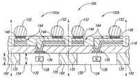
- FIG. 1Eis a schematic side cross-sectional view of the microelectronic device assembly 100 after encasing a portion of the dies 130 .
- an encapsulant 160is deposited onto the second surface 118 of the substrate 110 between adjacent dies 130 .
- the dies 130have a first thickness T 1
- the encapsulant 160has a second thickness T 2 at least approximately equal to the first thickness T 1 .
- the illustrated encapsulant 160encases the ends 135 of the dies 130 .
- the second thickness T 2 of the encapsulant 160can be less than or greater than the first thickness T 1 of the dies 130 .
- the encapsulantmay also encase the back sides 134 of the dies 130 .
- a plurality of electrical couplers 152are formed on corresponding contacts 146 .
- the electrical couplers 152are electrically connected to corresponding terminals 136 on the dies 130 , and thus the electrical couplers 152 , the contacts 146 , and the conductive lines 144 form a redistribution structure on the dies 130 .
- the microelectronic device assembly 100may not include the electrical couplers 152 , but rather wire-bonds can be attached to the contacts 146 . In either case, the microelectronic device assembly 100 is cut along lines A-A to singulate a plurality of individual microelectronic devices 102 (identified individually as 102 a - b ).
- the through holes 120are formed in the substrate 110 before the dies 130 are attached to the substrate 110 .
- This featurehas several advantages. First, the laser drilling, punching, or other process for forming the holes 120 in the substrate 110 does not damage the terminals 136 or other components on the active sides 132 of the dies 130 because the substrate 110 is detached from the dies 130 when the holes 120 are formed. As a result, the illustrated method is expected to increase the yield of the microelectronic devices 102 . Second, the microelectronic device assembly 100 does not require desmearing to remove residue and other debris from the terminals 136 on the dies 130 after forming the holes 120 .
- the illustrated methodreduces the number of processes required to construct the microelectronic devices 102 and increases the throughput.
- the preformed holes 120 in the substrate 110facilitate proper alignment of the dies 130 on the substrate 110 because the terminals 136 are visible through the holes 120 .
- the illustrated methodmay not require expensive alignment tools to ensure that the holes 120 are properly aligned with the terminals 136 .
- the dies 130can be known good dies.
- An advantage of this featureis that defective dies can be excluded from the microelectronic device assembly 100 . This increases the yield of the microelectronic devices 102 and reduces the number of devices 102 that malfunction and/or include defects.
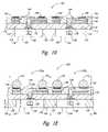
- FIGS. 2A and 2Billustrate stages in another embodiment of a method for manufacturing microelectronic devices.
- FIG. 2Ais a schematic side cross-sectional view of a substrate 210 and an adhesive layer 224 on the substrate 210 .
- the illustrated substrate 210is generally similar to the substrate 110 described above with reference to FIG. 1A .
- the substrate 210includes a first dielectric layer 212 , a first surface 216 , a second surface 218 opposite the first surface 216 , and a plurality of first holes 220 a extending between the first and second surfaces 216 and 218 .
- the substrate 210does not include a conductive layer
- the first dielectric layer 212includes a fully cured material.
- Suitable substratesinclude Upilex®-based materials manufactured by UBE Industries, Ltd. of Tokyo, Japan; Kapton or Microlux, both commercially available from E.I. du Pont de Nemours and Co. of Delaware, USA; and ESPANEX, commercially available from Nippon Steel Chemical Co., Ltd. of Tokyo, Japan; and other dielectric materials.
- the adhesive layer 224is positioned on the second surface 218 of the substrate 210 for attaching the substrate 210 to a plurality of singulated dies.
- the adhesive layer 224can be deposited onto the substrate 210 before or after constructing the first holes 220 a in the substrate 210 .
- the adhesive layer 224includes a plurality of second holes 220 b aligned with corresponding first holes 220 a in the substrate 210 .
- the first and second holes 220 a and 220 bform through holes 220 with a first dimension D 4 at the first surface 216 of the dielectric layer 212 and a second dimension D 5 at the adhesive layer 224 .
- the first dimension D 4is approximately equal to the second dimension D 5 ; however, in other embodiments, the first and second dimensions D 4 and D 5 can be different.
- the substrate 210may further include a conductive layer on the dielectric layer 212 .
- FIG. 2Bis a schematic side cross-sectional view of a microelectronic device assembly 200 in accordance with another embodiment of the invention.
- the microelectronic device assembly 200is generally similar to the microelectronic device assembly 100 described above with reference to FIGS. 1B-1E .
- the illustrated assembly 200includes the substrate 210 , a plurality of singulated dies 130 carried by the substrate 210 , and a redistribution structure formed at the substrate 210 .
- the active sides 132 of the dies 130are attached to the substrate 210 via the adhesive layer 224 .
- the illustrated redistribution structureincludes a plurality of conductive traces 244 electrically coupled to corresponding terminals 136 and a plurality of contacts 146 formed on corresponding conductive traces 244 .
- the individual conductive traces 244include a first conductive layer 240 disposed in the holes 220 ( FIG. 2A ) and on the first surface 216 of the substrate 210 and a second conductive layer 242 formed on the first conductive layer 240 .
- the illustrated contacts 146can be configured to receive electrical couplers (e.g., solder balls) or the ends of individual wire-bonds.
- the illustrated microelectronic device assembly 200further includes an encapsulant 260 encasing the ends 135 and the back side 134 of the individual dies 130 .
- the encapsulant 260may not cover the back sides 134 and/or the entire ends 135 of the dies.
- the microelectronic device assembly 200can be cut to singulate a plurality of individual microelectronic devices 202 (identified individually as 202 a - b ).
- FIGS. 3A and 3Billustrate stages in another embodiment of a method for manufacturing microelectronic devices.
- FIG. 3Ais a schematic side cross-sectional view of a substrate 310 and an adhesive layer 224 on the substrate 310 .
- the illustrated substrate 310is a preformed multi-layer substrate and includes a dielectric material 312 and a plurality of conductive traces 344 electrically isolated from each other.
- the substrate 310 and the adhesive layer 224further include a plurality of through holes 220 positioned such that each hole 220 exposes a corresponding conductive trace 344 .
- the adhesive layer 224may be a pre-preg material.
- FIG. 3Bis a schematic side cross-sectional view of a microelectronic device assembly 300 in accordance with another embodiment of the invention.
- the illustrated assembly 300is generally similar to the assembly 200 described above with reference to FIG. 2B .
- the assembly 300includes the substrate 310 , a plurality of singulated dies 130 carried by the substrate 310 , and a redistribution structure formed at the substrate 310 .
- the illustrated redistribution structureincludes a plurality of conductive links 342 formed in corresponding holes 220 ( FIG. 3A ) and electrically coupled to the associated conductive traces 344 .
- the individual conductive traces 344are electrically connected with corresponding terminals 136 on the dies 130 .
- the illustrated assembly 300further includes a plurality of electrical couplers 152 formed on corresponding conductive traces 344 and a dielectric layer 350 (e.g., solder mask) formed on the substrate 310 .
- the assembly 300may not include the electrical couplers 152 , but rather wire-bonds may electrically couple the conductive traces 344 to corresponding external contacts.
Landscapes
- Engineering & Computer Science (AREA)
- Microelectronics & Electronic Packaging (AREA)
- Computer Hardware Design (AREA)
- Power Engineering (AREA)
- Physics & Mathematics (AREA)
- Condensed Matter Physics & Semiconductors (AREA)
- General Physics & Mathematics (AREA)
- Manufacturing & Machinery (AREA)
- Encapsulation Of And Coatings For Semiconductor Or Solid State Devices (AREA)
- Production Of Multi-Layered Print Wiring Board (AREA)
- Perforating, Stamping-Out Or Severing By Means Other Than Cutting (AREA)
Abstract
Description
- The present invention is related to microelectronic devices and methods for manufacturing microelectronic devices.
- Microelectronic devices generally have a die (i.e., a chip) that includes integrated circuitry having a high density of very small components. In a typical process, a large number of dies are manufactured on a single wafer using many different processes that may be repeated at various stages (e.g., implanting, doping, photolithography, chemical vapor deposition, plasma vapor deposition, plating, planarizing, etching, etc.). The dies include an array of very small bond-pads electrically coupled to the integrated circuitry. The bond-pads are the external electrical contacts on the die through which the supply voltage, signals, etc., are transmitted to and from the integrated circuitry. After forming the dies, the wafer is thinned by backgrinding, and then the dies are separated from one another (i.e., singulated) by dicing the wafer. Next, the dies are typically “packaged” to connect the bond-pads to a larger array of electrical terminals that can be more easily coupled to the various power supply lines, signal lines, and ground lines.
- Conventional die-level packaging processes include (a) attaching individual dies to an interposer substrate, (b) wire-bonding the bond-pads of the dies to the terminals of the interposer substrate, and (c) encapsulating the dies with a molding compound. Die-level packaging, however, has several drawbacks. First, it is time consuming and expensive to mount individual dies to interposer substrates or lead frames. Second, as the demand for higher pin counts and smaller packages increases, it becomes more difficult to form robust wire-bonds that can withstand the forces involved in molding processes. Third, the handling processes for attaching individual dies to interposer substrates or lead frames may damage bare dies.
- Another process for packaging microelectronic devices is wafer-level packaging. In wafer-level packaging, a plurality of microelectronic dies are formed on a wafer, and then a redistribution layer is formed over the dies. The redistribution layer has a dielectric layer, a plurality of ball-pad arrays on the dielectric layer, and a plurality of conductive traces in the dielectric layer. Each ball-pad array is arranged over a corresponding die, and the ball-pads in each array are coupled to corresponding bond-pads of the die with the conductive traces. The conductive traces are typically constructed by laser drilling holes in the dielectric layer to expose the bond-pads on the dies, and then depositing conductive material into the holes. After forming the redistribution layer on the wafer, a highly accurate stenciling machine deposits discrete masses of solder paste onto the individual ball-pads. The solder paste is then reflowed to form small solder balls or “solder bumps” on the ball-pads. After forming the solder balls, the wafer is singulated to separate the individual microelectronic devices from one another. The individual microelectronic devices are subsequently attached to a substrate such as a printed circuit board. Microelectronic devices packaged at the wafer-level can have high pin counts in a small area, but they are not as robust as devices packaged at the die-level.
- Packaged microelectronic devices can also be constructed by “build-up” packaging. For example, a sacrificial substrate can be attached to a panel that includes a plurality of microelectronic dies and an organic filler that couples the dies together. The sacrificial substrate is generally a ceramic disc that is attached to the active sides of the dies. Next, the back sides of the dies are thinned and a ceramic layer is attached to the back sides. The sacrificial substrate is then removed from the active sides of the dies and build-up layers or a redistribution layer is formed on the active sides of the dies. Packaged devices using a build-up approach on a sacrificial substrate provide high pin counts in a small area and a reasonably robust structure.
- The build-up packaging process described above and conventional wafer-level packaging processes, however, have several drawbacks. First, laser drilling holes in the redistribution layer to expose the bond-pads can damage the bond-pads and/or other components on the active side of the dies. Second, because the dielectric layer covers the active side of the dies, it is difficult to properly align the laser beam with the bond-pads. Thus, laser drilling requires an expensive alignment tool to ensure that the holes are aligned with the bond-pads. Third, the bond-pads must be cleaned (e.g., desmeared) to remove residue and other debris after laser drilling the holes. Desmearing processes increase the costs of production and reduce throughput. Accordingly, there is a need to enhance the efficiency and reliability of packaging microelectronic devices.
FIGS. 1A-1E illustrate stages in one embodiment of a method for manufacturing a plurality of microelectronic devices.FIG. 1A is a schematic side cross-sectional view of a substrate for use in constructing the microelectronic devices.FIG. 1B is a schematic side cross-sectional view of a microelectronic device assembly including the substrate and a plurality of singulated dies arranged in an array on the substrate.FIG. 1C is a schematic side cross-sectional view of the microelectronic device assembly after depositing a third conductive layer onto the second conductive layer.FIG. 1D is a schematic side cross-sectional view of the microelectronic device assembly after depositing a second dielectric layer onto the conductive lines and the first dielectric layer.FIG. 1E is a schematic side cross-sectional view of the microelectronic device assembly after encasing a portion of the dies.FIGS. 2A and 2B illustrate stages in another embodiment of a method for manufacturing microelectronic devices.FIG. 2A is a schematic side cross-sectional view of a substrate and an adhesive layer on the substrate.FIG. 2B is a schematic side cross-sectional view of a microelectronic device assembly.FIGS. 3A and 3B illustrate stages in another embodiment of a method for manufacturing microelectronic devices.FIG. 3A is a schematic side cross-sectional view of a substrate and an adhesive layer on the substrate.FIG. 3B is a schematic side cross-sectional view of a microelectronic device assembly.- The following disclosure describes several embodiments of microelectronic devices and methods for manufacturing microelectronic devices. An embodiment of one such method includes (a) providing a substrate having a dielectric layer and a plurality of through holes arranged in arrays, and (b) attaching a plurality of singulated microelectronic dies to the substrate with an active side of the individual dies facing toward the substrate and with a plurality of terminals on the active side of the individual dies aligned with corresponding holes in the substrate. The singulated dies are attached to the substrate after forming the holes in the substrate.
- In another embodiment, a method includes providing a plurality of singulated microelectronic dies and a substrate with a plurality of holes arranged in arrays. The individual dies include an active side and a plurality of terminals at the active side. The method further includes (a) coupling the active sides of the singulated dies to the substrate such that the terminals are aligned with corresponding holes, and (b) forming a redistribution structure at the substrate. The redistribution structure includes a plurality of contacts electrically coupled to corresponding terminals on the dies.
- In another embodiment, a method includes attaching a plurality of singulated microelectronic dies to a partially cured substrate with an active side of the individual dies facing toward the substrate. The partially cured substrate has a plurality of through apertures, and the individual dies further include a plurality of terminals aligned with corresponding apertures. The method further includes curing the substrate after attaching the singulated dies and constructing a redistribution structure at the substrate. The redistribution structure includes a plurality of conductive lines electrically coupled to corresponding terminals on the dies.
- Another aspect of the invention is directed to a microelectronic device assembly. In one embodiment, a microelectronic device assembly includes a substrate having a plurality of holes arranged in arrays and a plurality of singulated microelectronic dies attached to the substrate. The individual dies include an active side facing toward the substrate, a plurality of terminals disposed on the active side and aligned with corresponding holes, a back side opposite the active side, and a plurality of ends extending between the active side and the back side. At least a portion of the individual ends of the dies are exposed.
- In another embodiment, a microelectronic device assembly includes a partially cured substrate having a plurality of through holes and a plurality of microelectronic dies attached to the substrate. The individual dies include an active side facing toward the substrate, a plurality of terminals disposed on the active side and aligned with corresponding holes, and an integrated circuit operably coupled to the terminals.
- Another aspect of the invention is directed to microelectronic devices. In one embodiment, a microelectronic device includes a preformed substrate having a plurality of through holes arranged in an array and a microelectronic die attached to the substrate. The die includes an active side facing toward the substrate, a plurality of terminals disposed on the active side and aligned with corresponding holes, and an integrated circuit operably coupled to the terminals.
- Specific details of several embodiments of the invention are described below with reference to microelectronic devices including microelectronic dies, but in other embodiments the microelectronic devices can include other components. For example, the microelectronic devices can include micromechanical components, data storage elements, optics, read/write components, or other features. The microelectronic dies can be SRAM, DRAM (e.g., DDR-SDRAM), flash-memory (e.g., NAND flash-memory), processors, and other types of devices. Moreover, although the illustrated microelectronic devices are constructed at the wafer level, in additional embodiments the microelectronic devices can be manufactured at the die level. Also, several other embodiments of the invention can have different configurations, components, or procedures than those described in this section. A person of ordinary skill in the art, therefore, will accordingly understand that the invention may have other embodiments with additional elements, or the invention may have other embodiments without several of the elements shown and described below with reference to
FIGS. 1A-3B . FIGS. 1A-1E illustrate stages in one embodiment of a method for manufacturing a plurality of microelectronic devices. For example,FIG. 1A is a schematic side cross-sectional view of asubstrate 110 including a firstdielectric layer 112 and a firstconductive layer 114 on thedielectric layer 112. Thefirst dielectric layer 112 can include a partially cured material (e.g., B-stage material) for subsequently attaching thesubstrate 110 to a plurality of dies. For example, thefirst dielectric layer 112 can be a resin coated copper (RCC) or pre-preg material with woven fiber cloth embedded in a B-stage resin. The firstconductive layer 114 can be a foil (e.g., copper foil) formed on thefirst dielectric layer 112.Suitable substrates 110 include Product No. MCF-6000E manufactured by Hitachi Chemical Co. America, Ltd. of Cupertino, Calif. In other embodiments, such as the embodiments described below with reference toFIGS. 2A-3B , the substrate may not include the first conductive layer, and/or thefirst dielectric layer 112 may include a fully cured material.- The illustrated
substrate 110 further includes afirst surface 116 at the firstconductive layer 114, asecond surface 118 at thefirst dielectric layer 112, and a plurality of throughholes 120 extending between the first andsecond surfaces holes 120 are arranged in arrays with each array corresponding to an arrangement of terminals on a die that is subsequently attached to thesubstrate 110. Theindividual holes 120 can have a first dimension D1at thefirst surface 116 and a second dimension D2at thesecond surface 118. In the illustrated embodiment, the first dimension D1is greater than the second dimension D2, but in other embodiments the first dimension D1can be generally equal to or less than the second dimension D2. - The
individual holes 120 include afirst portion 122ain the firstconductive layer 114 and asecond portion 122bin thefirst dielectric layer 112. The first and second portions122a-bcan be formed with different processes. For example, thefirst portion 122acan be formed by placing a photoresist on thefirst surface 116 of thesubstrate 110, patterning and developing the photoresist, and etching the firstconductive layer 114 to remove selected portions of thelayer 114. Thesecond portion 122bcan be formed by laser drilling, punching, etching, or other suitable processes. In additional embodiments, the first and second portions122a-bof theholes 120 can be formed by the same process. FIG. 1B is a schematic side cross-sectional view of amicroelectronic device assembly 100 including thesubstrate 110 and a plurality of singulated dies130 arranged in an array on thesubstrate 110. The individual dies130 include anactive side 132, aback side 134 opposite theactive side 132, a plurality ofends 135 extending between theactive side 132 and theback side 134, a plurality of terminals136 (e.g., bond-pads) arranged in an array on theactive side 132, and an integrated circuit138 (shown schematically) operably coupled to theterminals 136. The dies130 are attached to thesubstrate 110 with theactive sides 132 facing thesecond surface 118 and with theterminals 136 aligned with correspondingholes 120 such that theterminals 136 and theholes 120 have a one-to-one correspondence. Theindividual terminals 136 may have a dimension D3greater than the second dimension D2(FIG. 1A ) of theholes 120 to facilitate proper alignment. In the illustrated embodiment, the dies130 are attached to thesubstrate 110 without an adhesive positioned between thesecond surface 118 and theactive sides 132. Rather, the adhesive properties of the partially cured material in thefirst dielectric layer 112 enable the dies130 to remain attached to thesubstrate 110. In other embodiments, such as the embodiments described below with reference toFIGS. 2A-3B , the microelectronic device assembly may include an adhesive for attaching the dies130 to thesubstrate 110. Moreover, although the illustrated dies130 have the same structure, in other embodiments the dies may have different features to perform different functions. In another embodiment, themicroelectronic device assembly 100 may include thesubstrate 110 and a plurality of microelectronic components other than dies. For example, a plurality of capacitors, resistors, inductors, or other devices can be attached to thesubstrate 110 with the terminals on these devices aligned with correspondingholes 120 in thesubstrate 110.- After attaching the dies130 to the
substrate 110, themicroelectronic device assembly 100 can be heated to fully cure the partially cured material in thedielectric layer 112 and ensure the dies130 remain connected to thesubstrate 110. In other embodiments, such as embodiments in which thedielectric layer 112 does not include a partially cured material, the microelectronic device assembly may not be heated after attaching the dies130 to thesubstrate 110. In either case, after die attachment, a secondconductive layer 140 is deposited onto thesubstrate 110. Specifically, the secondconductive layer 140 is placed in theholes 120 and over thefirst surface 116 of thesubstrate 110. The secondconductive layer 140 can be formed on thesubstrate 110 by electroless plating, physical vapor deposition, sputtering, or other suitable processes. In several embodiments, in which theterminals 136 do not have a surface compatible with electroless plating, additional processes such as zincation, sputtering, and/or plating may be necessary to deposit a compatible conductive protective layer (e.g., a nickel layer) on theterminals 136 before depositing the secondconductive layer 140. The conductive protective layer prevents the plating solution from damaging theterminals 136. FIG. 1C is a schematic side cross-sectional view of themicroelectronic device assembly 100 after depositing a thirdconductive layer 142 onto the secondconductive layer 140. The thirdconductive layer 142 can be formed by depositing a dry film across the secondconductive layer 140, patterning the dry film, and electroplating material onto the exposed sections of the secondconductive layer 140. In other embodiments, the thirdconductive layer 142 can be deposited across the entire secondconductive layer 140, or the second and thirdconductive layers conductive layer 142, sections of the first, second, and/or thirdconductive layers substrate 110. Eachconductive line 144 is electrically coupled to acorresponding terminal 136 on adie 130, and theconductive lines 144 are spaced apart from each other.FIG. 1D is a schematic side cross-sectional view of themicroelectronic device assembly 100 after depositing asecond dielectric layer 150 onto theconductive lines 144 and thefirst dielectric layer 112. Thesecond dielectric layer 150 can be a solder mask or other suitable material for protecting and electrically isolating theconductive lines 144. After forming thesecond dielectric layer 150, portions of thelayer 150 are removed to expose sections of theconductive lines 144 and a plurality ofcontacts 146 can be formed on exposed sections of correspondingconductive lines 144. Thecontacts 146 may be constructed by electroplating or other suitable processes.FIG. 1E is a schematic side cross-sectional view of themicroelectronic device assembly 100 after encasing a portion of the dies130. After forming thecontacts 146, anencapsulant 160 is deposited onto thesecond surface 118 of thesubstrate 110 between adjacent dies130. In the illustrated embodiment, the dies130 have a first thickness T1, and theencapsulant 160 has a second thickness T2at least approximately equal to the first thickness T1. As a result, the illustratedencapsulant 160 encases theends 135 of the dies130. In other embodiments, the second thickness T2of theencapsulant 160 can be less than or greater than the first thickness T1of the dies130. For example, the encapsulant may also encase theback sides 134 of the dies130.- After encasing at least a portion of the individual dies130, a plurality of electrical couplers152 (e.g., solder balls) are formed on
corresponding contacts 146. Theelectrical couplers 152 are electrically connected to correspondingterminals 136 on the dies130, and thus theelectrical couplers 152, thecontacts 146, and theconductive lines 144 form a redistribution structure on the dies130. In other embodiments, themicroelectronic device assembly 100 may not include theelectrical couplers 152, but rather wire-bonds can be attached to thecontacts 146. In either case, themicroelectronic device assembly 100 is cut along lines A-A to singulate a plurality of individual microelectronic devices102 (identified individually as102a-b). - One feature of the embodiment of the method illustrated above with reference to
FIGS. 1A-1E is that the throughholes 120 are formed in thesubstrate 110 before the dies130 are attached to thesubstrate 110. This feature has several advantages. First, the laser drilling, punching, or other process for forming theholes 120 in thesubstrate 110 does not damage theterminals 136 or other components on theactive sides 132 of the dies130 because thesubstrate 110 is detached from the dies130 when theholes 120 are formed. As a result, the illustrated method is expected to increase the yield of the microelectronic devices102. Second, themicroelectronic device assembly 100 does not require desmearing to remove residue and other debris from theterminals 136 on the dies130 after forming theholes 120. Accordingly, the illustrated method reduces the number of processes required to construct the microelectronic devices102 and increases the throughput. Third, the preformedholes 120 in thesubstrate 110 facilitate proper alignment of the dies130 on thesubstrate 110 because theterminals 136 are visible through theholes 120. Thus, the illustrated method may not require expensive alignment tools to ensure that theholes 120 are properly aligned with theterminals 136. - Another feature of the embodiment of the method illustrated above with reference to
FIGS. 1A-1E is that the dies130 can be known good dies. An advantage of this feature is that defective dies can be excluded from themicroelectronic device assembly 100. This increases the yield of the microelectronic devices102 and reduces the number of devices102 that malfunction and/or include defects. FIGS. 2A and 2B illustrate stages in another embodiment of a method for manufacturing microelectronic devices. For example,FIG. 2A is a schematic side cross-sectional view of asubstrate 210 and anadhesive layer 224 on thesubstrate 210. The illustratedsubstrate 210 is generally similar to thesubstrate 110 described above with reference toFIG. 1A . For example, thesubstrate 210 includes a firstdielectric layer 212, afirst surface 216, asecond surface 218 opposite thefirst surface 216, and a plurality offirst holes 220aextending between the first andsecond surfaces substrate 210 does not include a conductive layer, and thefirst dielectric layer 212 includes a fully cured material. Suitable substrates include Upilex®-based materials manufactured by UBE Industries, Ltd. of Tokyo, Japan; Kapton or Microlux, both commercially available from E.I. du Pont de Nemours and Co. of Delaware, USA; and ESPANEX, commercially available from Nippon Steel Chemical Co., Ltd. of Tokyo, Japan; and other dielectric materials.- The
adhesive layer 224 is positioned on thesecond surface 218 of thesubstrate 210 for attaching thesubstrate 210 to a plurality of singulated dies. Theadhesive layer 224 can be deposited onto thesubstrate 210 before or after constructing thefirst holes 220ain thesubstrate 210. In either case, theadhesive layer 224 includes a plurality ofsecond holes 220baligned with correspondingfirst holes 220ain thesubstrate 210. The first andsecond holes holes 220 with a first dimension D4at thefirst surface 216 of thedielectric layer 212 and a second dimension D5at theadhesive layer 224. In the illustrated embodiment, the first dimension D4is approximately equal to the second dimension D5; however, in other embodiments, the first and second dimensions D4and D5can be different. In additional embodiments, thesubstrate 210 may further include a conductive layer on thedielectric layer 212. FIG. 2B is a schematic side cross-sectional view of amicroelectronic device assembly 200 in accordance with another embodiment of the invention. Themicroelectronic device assembly 200 is generally similar to themicroelectronic device assembly 100 described above with reference toFIGS. 1B-1E . For example, the illustratedassembly 200 includes thesubstrate 210, a plurality of singulated dies130 carried by thesubstrate 210, and a redistribution structure formed at thesubstrate 210. In the illustratedassembly 200, however, theactive sides 132 of the dies130 are attached to thesubstrate 210 via theadhesive layer 224. Moreover, the illustrated redistribution structure includes a plurality ofconductive traces 244 electrically coupled tocorresponding terminals 136 and a plurality ofcontacts 146 formed on corresponding conductive traces244. The individualconductive traces 244 include a firstconductive layer 240 disposed in the holes220 (FIG. 2A ) and on thefirst surface 216 of thesubstrate 210 and a secondconductive layer 242 formed on the firstconductive layer 240. The illustratedcontacts 146 can be configured to receive electrical couplers (e.g., solder balls) or the ends of individual wire-bonds. The illustratedmicroelectronic device assembly 200 further includes anencapsulant 260 encasing theends 135 and theback side 134 of the individual dies130. In other embodiments, theencapsulant 260 may not cover theback sides 134 and/or the entire ends135 of the dies. After construction, themicroelectronic device assembly 200 can be cut to singulate a plurality of individual microelectronic devices202 (identified individually as202a-b).FIGS. 3A and 3B illustrate stages in another embodiment of a method for manufacturing microelectronic devices. For example,FIG. 3A is a schematic side cross-sectional view of asubstrate 310 and anadhesive layer 224 on thesubstrate 310. The illustratedsubstrate 310 is a preformed multi-layer substrate and includes adielectric material 312 and a plurality ofconductive traces 344 electrically isolated from each other. Thesubstrate 310 and theadhesive layer 224 further include a plurality of throughholes 220 positioned such that eachhole 220 exposes a correspondingconductive trace 344. In several embodiments, theadhesive layer 224 may be a pre-preg material.FIG. 3B is a schematic side cross-sectional view of amicroelectronic device assembly 300 in accordance with another embodiment of the invention. The illustratedassembly 300 is generally similar to theassembly 200 described above with reference toFIG. 2B . For example, theassembly 300 includes thesubstrate 310, a plurality of singulated dies130 carried by thesubstrate 310, and a redistribution structure formed at thesubstrate 310. The illustrated redistribution structure includes a plurality ofconductive links 342 formed in corresponding holes220 (FIG. 3A ) and electrically coupled to the associated conductive traces344. As such, the individualconductive traces 344 are electrically connected withcorresponding terminals 136 on the dies130. The illustratedassembly 300 further includes a plurality ofelectrical couplers 152 formed on correspondingconductive traces 344 and a dielectric layer350 (e.g., solder mask) formed on thesubstrate 310. In other embodiments, theassembly 300 may not include theelectrical couplers 152, but rather wire-bonds may electrically couple theconductive traces 344 to corresponding external contacts.- From the foregoing, it will be appreciated that specific embodiments of the invention have been described herein for purposes of illustration, but that various modifications may be made without deviating from the spirit and scope of the invention. For example, many of the elements of one embodiment can be combined with other embodiments in addition to or in lieu of the elements of the other embodiments. Accordingly, the invention is not limited except as by the appended claims.
Claims (48)
Priority Applications (2)
| Application Number | Priority Date | Filing Date | Title |
|---|---|---|---|
| US12/474,465US8310048B2 (en) | 2006-08-04 | 2009-05-29 | Microelectronic devices |
| US13/675,523US8742572B2 (en) | 2006-08-04 | 2012-11-13 | Microelectronic devices and methods for manufacturing microelectronic devices |
Applications Claiming Priority (2)
| Application Number | Priority Date | Filing Date | Title |
|---|---|---|---|
| SG200605271-6ASG139594A1 (en) | 2006-08-04 | 2006-08-04 | Microelectronic devices and methods for manufacturing microelectronic devices |
| SG200605271-6 | 2006-08-04 |
Related Child Applications (1)
| Application Number | Title | Priority Date | Filing Date |
|---|---|---|---|
| US12/474,465DivisionUS8310048B2 (en) | 2006-08-04 | 2009-05-29 | Microelectronic devices |
Publications (2)
| Publication Number | Publication Date |
|---|---|
| US20080032447A1true US20080032447A1 (en) | 2008-02-07 |
| US7553699B2 US7553699B2 (en) | 2009-06-30 |
Family
ID=39029697
Family Applications (3)
| Application Number | Title | Priority Date | Filing Date |
|---|---|---|---|
| US11/515,090ActiveUS7553699B2 (en) | 2006-08-04 | 2006-08-31 | Method of fabricating microelectronic devices |
| US12/474,465ActiveUS8310048B2 (en) | 2006-08-04 | 2009-05-29 | Microelectronic devices |
| US13/675,523ActiveUS8742572B2 (en) | 2006-08-04 | 2012-11-13 | Microelectronic devices and methods for manufacturing microelectronic devices |
Family Applications After (2)
| Application Number | Title | Priority Date | Filing Date |
|---|---|---|---|
| US12/474,465ActiveUS8310048B2 (en) | 2006-08-04 | 2009-05-29 | Microelectronic devices |
| US13/675,523ActiveUS8742572B2 (en) | 2006-08-04 | 2012-11-13 | Microelectronic devices and methods for manufacturing microelectronic devices |
Country Status (2)
| Country | Link |
|---|---|
| US (3) | US7553699B2 (en) |
| SG (1) | SG139594A1 (en) |
Cited By (17)
| Publication number | Priority date | Publication date | Assignee | Title |
|---|---|---|---|---|
| US20090236736A1 (en)* | 2006-08-04 | 2009-09-24 | Micron Technology, Inc. | Microelectronic devices and methods for manufacturing microelectronic devices |
| US20100155126A1 (en)* | 2008-12-24 | 2010-06-24 | Shinko Electric Industries Co., Ltd. | Fine wiring package and method of manufacturing the same |
| US20100155925A1 (en)* | 2008-12-24 | 2010-06-24 | Shinko Electric Industries Co., Ltd. | Resin-sealed package and method of producing the same |
| US20100244235A1 (en)* | 2009-03-24 | 2010-09-30 | Christopher James Kapusta | Integrated circuit package and method of making same |
| US20110133324A1 (en)* | 2009-12-03 | 2011-06-09 | Powertech Technology Inc. | Multi-chip stacked package and its mother chip to save interposer |
| US20110156261A1 (en)* | 2009-03-24 | 2011-06-30 | Christopher James Kapusta | Integrated circuit package and method of making same |
| EP2673801A1 (en)* | 2011-02-09 | 2013-12-18 | Robert Bosch GmbH | Contact system comprising a connecting means and method |
| US20150380386A1 (en)* | 2014-06-26 | 2015-12-31 | Michael B. Vincent | Microelectronic packages having embedded sidewall substrates and methods for the producing thereof |
| EP3029719A1 (en)* | 2014-12-01 | 2016-06-08 | General Electric Company | Electronic packages and methods of making and using the same |
| KR20170069925A (en)* | 2015-12-11 | 2017-06-21 | 가부시키가이샤 제이디바이스 | Wiring board, semiconductor package including wiring board and manufacturing method thereof |
| EP2469591A3 (en)* | 2010-12-22 | 2018-01-31 | General Electric Company | Method for fabricating a semiconductor device package |
| US20180061798A1 (en)* | 2013-08-29 | 2018-03-01 | Taiwan Semiconductor Manufacturing Company Ltd. | Semiconductor device and manufacturing method thereof |
| US20220399254A1 (en)* | 2021-06-11 | 2022-12-15 | Jcet Group Co., Ltd. | Package structure and method for manufacturing same |
| US11605569B2 (en)* | 2018-04-19 | 2023-03-14 | AT&SAustria Technologie & Systemtechnik AG | Packaged integrated circuit with interposing functionality and method for manufacturing such a packaged integrated circuit |
| US11716816B2 (en) | 2003-09-18 | 2023-08-01 | Imberatek, Llc | Method for manufacturing an electronic module and electronic module |
| US11792941B2 (en) | 2005-06-16 | 2023-10-17 | Imberatek, Llc | Circuit board structure and method for manufacturing a circuit board structure |
| USRE49970E1 (en) | 2009-05-19 | 2024-05-14 | Imberatek, Llc | Manufacturing method and electronic module with new routing possibilities |
Families Citing this family (11)
| Publication number | Priority date | Publication date | Assignee | Title |
|---|---|---|---|---|
| US8021981B2 (en)* | 2006-08-30 | 2011-09-20 | Micron Technology, Inc. | Redistribution layers for microfeature workpieces, and associated systems and methods |
| US8101464B2 (en) | 2006-08-30 | 2012-01-24 | Micron Technology, Inc. | Microelectronic devices and methods for manufacturing microelectronic devices |
| WO2009020467A1 (en)* | 2007-08-07 | 2009-02-12 | Skyworks Solutions, Inc. | Near chip scale package integration process |
| US8030780B2 (en) | 2008-10-16 | 2011-10-04 | Micron Technology, Inc. | Semiconductor substrates with unitary vias and via terminals, and associated systems and methods |
| TWI402003B (en)* | 2009-10-16 | 2013-07-11 | Princo Corp | Metal structure of flexible multi-layer substrate and manufacturing method thereof |
| US8969176B2 (en)* | 2010-12-03 | 2015-03-03 | Raytheon Company | Laminated transferable interconnect for microelectronic package |
| US20120161319A1 (en)* | 2010-12-23 | 2012-06-28 | Stmicroelectronics Pte Ltd. | Ball grid array method and structure |
| US8643184B1 (en) | 2012-10-31 | 2014-02-04 | Intel Corporation | Crosstalk polarity reversal and cancellation through substrate material tuning |
| US9184104B1 (en)* | 2014-05-28 | 2015-11-10 | Stats Chippac, Ltd. | Semiconductor device and method of forming adhesive layer over insulating layer for bonding carrier to mixed surfaces of semiconductor die and encapsulant |
| US10192840B2 (en)* | 2015-09-25 | 2019-01-29 | Intel Corporation | Ball pad with a plurality of lobes |
| US20240145258A1 (en)* | 2022-10-27 | 2024-05-02 | Stmicroelectronics Pte Ltd | Panel level semiconductor package and method of manufacturing the same |
Citations (17)
| Publication number | Priority date | Publication date | Assignee | Title |
|---|---|---|---|---|
| US4783695A (en)* | 1986-09-26 | 1988-11-08 | General Electric Company | Multichip integrated circuit packaging configuration and method |
| US5510139A (en)* | 1992-01-16 | 1996-04-23 | Ameg Additive Metallisierung-Entwicklunge-Und Anwendungssesellshaft Gmbh | Process for assembly and bonding of electronic components on an insulating support |
| US6048755A (en)* | 1998-11-12 | 2000-04-11 | Micron Technology, Inc. | Method for fabricating BGA package using substrate with patterned solder mask open in die attach area |
| US6159767A (en)* | 1996-05-20 | 2000-12-12 | Epic Technologies, Inc. | Single chip modules, repairable multichip modules, and methods of fabrication thereof |
| US6426241B1 (en)* | 1999-11-12 | 2002-07-30 | International Business Machines Corporation | Method for forming three-dimensional circuitization and circuits formed |
| US6637103B2 (en)* | 1999-08-18 | 2003-10-28 | Micron Technology, Inc. | Method of tape bonding |
| US6721469B2 (en)* | 2001-12-06 | 2004-04-13 | Chiral Photonics, Inc. | Chiral in-fiber adjustable polarizer apparatus and method |
| US6818544B2 (en)* | 2000-02-10 | 2004-11-16 | Epic Technologies, Inc. | Compliant, solderable input/output bump structures |
| US6917107B2 (en)* | 1999-09-02 | 2005-07-12 | Micron Technology, Inc. | Board-on-chip packages |
| US20050287708A1 (en)* | 2004-06-24 | 2005-12-29 | Kim Sang-Young | Semiconductor chip package manufacturing method including screen printing process |
| US6982475B1 (en)* | 1998-03-20 | 2006-01-03 | Mcsp, Llc | Hermetic wafer scale integrated circuit structure |
| US20060046347A1 (en)* | 2004-09-02 | 2006-03-02 | Wood Alan G | Die package, conductive element, semiconductor device including same, microlens, system including same, and methods of manufacture |
| US7041534B2 (en)* | 2003-08-28 | 2006-05-09 | Advanced Semiconductor Engineering, Inc. | Semiconductor chip package and method for making the same |
| US20060125103A1 (en)* | 2004-03-31 | 2006-06-15 | Endicott Interconnect Technologies, Inc. | Information handling system |
| US20060157864A1 (en)* | 2005-01-12 | 2006-07-20 | Industrial Technology Research Institute | Electronic device package and method of manufacturing the same |
| US20070182000A1 (en)* | 2002-02-19 | 2007-08-09 | Matsushita Electric Industrial Co., Ltd. | Module part |
| US20070267136A1 (en)* | 2004-11-26 | 2007-11-22 | Tuominen Risto | Method for Manufacturing an Electronics Module |
Family Cites Families (6)
| Publication number | Priority date | Publication date | Assignee | Title |
|---|---|---|---|---|
| JP3763962B2 (en) | 1998-03-11 | 2006-04-05 | 株式会社フジクラ | Mounting method of chip parts on printed circuit board |
| US6337228B1 (en)* | 1999-05-12 | 2002-01-08 | Amkor Technology, Inc. | Low-cost printed circuit board with integral heat sink for semiconductor package |
| US6271469B1 (en) | 1999-11-12 | 2001-08-07 | Intel Corporation | Direct build-up layer on an encapsulated die package |
| JP4093186B2 (en)* | 2004-01-27 | 2008-06-04 | カシオ計算機株式会社 | Manufacturing method of semiconductor device |
| TWI241697B (en) | 2005-01-06 | 2005-10-11 | Siliconware Precision Industries Co Ltd | Semiconductor package and fabrication method thereof |
| SG139594A1 (en)* | 2006-08-04 | 2008-02-29 | Micron Technology Inc | Microelectronic devices and methods for manufacturing microelectronic devices |
- 2006
- 2006-08-04SGSG200605271-6Apatent/SG139594A1/enunknown
- 2006-08-31USUS11/515,090patent/US7553699B2/enactiveActive
- 2009
- 2009-05-29USUS12/474,465patent/US8310048B2/enactiveActive
- 2012
- 2012-11-13USUS13/675,523patent/US8742572B2/enactiveActive
Patent Citations (17)
| Publication number | Priority date | Publication date | Assignee | Title |
|---|---|---|---|---|
| US4783695A (en)* | 1986-09-26 | 1988-11-08 | General Electric Company | Multichip integrated circuit packaging configuration and method |
| US5510139A (en)* | 1992-01-16 | 1996-04-23 | Ameg Additive Metallisierung-Entwicklunge-Und Anwendungssesellshaft Gmbh | Process for assembly and bonding of electronic components on an insulating support |
| US6159767A (en)* | 1996-05-20 | 2000-12-12 | Epic Technologies, Inc. | Single chip modules, repairable multichip modules, and methods of fabrication thereof |
| US6982475B1 (en)* | 1998-03-20 | 2006-01-03 | Mcsp, Llc | Hermetic wafer scale integrated circuit structure |
| US6048755A (en)* | 1998-11-12 | 2000-04-11 | Micron Technology, Inc. | Method for fabricating BGA package using substrate with patterned solder mask open in die attach area |
| US6637103B2 (en)* | 1999-08-18 | 2003-10-28 | Micron Technology, Inc. | Method of tape bonding |
| US6917107B2 (en)* | 1999-09-02 | 2005-07-12 | Micron Technology, Inc. | Board-on-chip packages |
| US6426241B1 (en)* | 1999-11-12 | 2002-07-30 | International Business Machines Corporation | Method for forming three-dimensional circuitization and circuits formed |
| US6818544B2 (en)* | 2000-02-10 | 2004-11-16 | Epic Technologies, Inc. | Compliant, solderable input/output bump structures |
| US6721469B2 (en)* | 2001-12-06 | 2004-04-13 | Chiral Photonics, Inc. | Chiral in-fiber adjustable polarizer apparatus and method |
| US20070182000A1 (en)* | 2002-02-19 | 2007-08-09 | Matsushita Electric Industrial Co., Ltd. | Module part |
| US7041534B2 (en)* | 2003-08-28 | 2006-05-09 | Advanced Semiconductor Engineering, Inc. | Semiconductor chip package and method for making the same |
| US20060125103A1 (en)* | 2004-03-31 | 2006-06-15 | Endicott Interconnect Technologies, Inc. | Information handling system |
| US20050287708A1 (en)* | 2004-06-24 | 2005-12-29 | Kim Sang-Young | Semiconductor chip package manufacturing method including screen printing process |
| US20060046347A1 (en)* | 2004-09-02 | 2006-03-02 | Wood Alan G | Die package, conductive element, semiconductor device including same, microlens, system including same, and methods of manufacture |
| US20070267136A1 (en)* | 2004-11-26 | 2007-11-22 | Tuominen Risto | Method for Manufacturing an Electronics Module |
| US20060157864A1 (en)* | 2005-01-12 | 2006-07-20 | Industrial Technology Research Institute | Electronic device package and method of manufacturing the same |
Cited By (29)
| Publication number | Priority date | Publication date | Assignee | Title |
|---|---|---|---|---|
| US11716816B2 (en) | 2003-09-18 | 2023-08-01 | Imberatek, Llc | Method for manufacturing an electronic module and electronic module |
| US11792941B2 (en) | 2005-06-16 | 2023-10-17 | Imberatek, Llc | Circuit board structure and method for manufacturing a circuit board structure |
| US20090236736A1 (en)* | 2006-08-04 | 2009-09-24 | Micron Technology, Inc. | Microelectronic devices and methods for manufacturing microelectronic devices |
| US8310048B2 (en) | 2006-08-04 | 2012-11-13 | Micron Technology, Inc. | Microelectronic devices |
| US8399977B2 (en)* | 2008-12-24 | 2013-03-19 | Shinko Electric Industries Co., Ltd. | Resin-sealed package and method of producing the same |
| US20100155126A1 (en)* | 2008-12-24 | 2010-06-24 | Shinko Electric Industries Co., Ltd. | Fine wiring package and method of manufacturing the same |
| US20100155925A1 (en)* | 2008-12-24 | 2010-06-24 | Shinko Electric Industries Co., Ltd. | Resin-sealed package and method of producing the same |
| US8530753B2 (en) | 2008-12-24 | 2013-09-10 | Shinko Electric Industries Co., Ltd. | Fine wiring package and method of manufacturing the same |
| US9299661B2 (en) | 2009-03-24 | 2016-03-29 | General Electric Company | Integrated circuit package and method of making same |
| US20110156261A1 (en)* | 2009-03-24 | 2011-06-30 | Christopher James Kapusta | Integrated circuit package and method of making same |
| US20100244235A1 (en)* | 2009-03-24 | 2010-09-30 | Christopher James Kapusta | Integrated circuit package and method of making same |
| USRE49970E1 (en) | 2009-05-19 | 2024-05-14 | Imberatek, Llc | Manufacturing method and electronic module with new routing possibilities |
| US8304917B2 (en)* | 2009-12-03 | 2012-11-06 | Powertech Technology Inc. | Multi-chip stacked package and its mother chip to save interposer |
| US20110133324A1 (en)* | 2009-12-03 | 2011-06-09 | Powertech Technology Inc. | Multi-chip stacked package and its mother chip to save interposer |
| EP2469591A3 (en)* | 2010-12-22 | 2018-01-31 | General Electric Company | Method for fabricating a semiconductor device package |
| EP2673801A1 (en)* | 2011-02-09 | 2013-12-18 | Robert Bosch GmbH | Contact system comprising a connecting means and method |
| US20180061798A1 (en)* | 2013-08-29 | 2018-03-01 | Taiwan Semiconductor Manufacturing Company Ltd. | Semiconductor device and manufacturing method thereof |
| US10971463B2 (en)* | 2013-08-29 | 2021-04-06 | Taiwan Semiconductor Manufacturing Company Ltd. | Interconnection structure including a metal post encapsulated by a joint material having concave outer surface |
| US9595485B2 (en)* | 2014-06-26 | 2017-03-14 | Nxp Usa, Inc. | Microelectronic packages having embedded sidewall substrates and methods for the producing thereof |
| US20150380386A1 (en)* | 2014-06-26 | 2015-12-31 | Michael B. Vincent | Microelectronic packages having embedded sidewall substrates and methods for the producing thereof |
| EP3029719A1 (en)* | 2014-12-01 | 2016-06-08 | General Electric Company | Electronic packages and methods of making and using the same |
| CN107039391A (en)* | 2015-12-11 | 2017-08-11 | 株式会社吉帝伟士 | Wiring substrate, semiconductor package having wiring substrate, and manufacturing method thereof |
| KR20170069925A (en)* | 2015-12-11 | 2017-06-21 | 가부시키가이샤 제이디바이스 | Wiring board, semiconductor package including wiring board and manufacturing method thereof |
| KR102584116B1 (en) | 2015-12-11 | 2023-10-04 | 가부시키가이샤 앰코테크놀로지재팬 | Wiring board, semiconductor package including wiring board and manufacturing method thereof |
| KR20230142406A (en)* | 2015-12-11 | 2023-10-11 | 가부시키가이샤 앰코테크놀로지재팬 | Wiring board, semiconductor package including wiring board and manufacturing method thereof |
| KR102742559B1 (en) | 2015-12-11 | 2024-12-17 | 가부시키가이샤 앰코테크놀로지재팬 | Wiring board, semiconductor package including wiring board and manufacturing method thereof |
| US11605569B2 (en)* | 2018-04-19 | 2023-03-14 | AT&SAustria Technologie & Systemtechnik AG | Packaged integrated circuit with interposing functionality and method for manufacturing such a packaged integrated circuit |
| US20220399254A1 (en)* | 2021-06-11 | 2022-12-15 | Jcet Group Co., Ltd. | Package structure and method for manufacturing same |
| US11854949B2 (en)* | 2021-06-11 | 2023-12-26 | Jcet Group Co., Ltd. | Package structure having a plurality of chips attached to a lead frame by redistribution layer |
Also Published As
| Publication number | Publication date |
|---|---|
| US8310048B2 (en) | 2012-11-13 |
| US20090236736A1 (en) | 2009-09-24 |
| US7553699B2 (en) | 2009-06-30 |
| US8742572B2 (en) | 2014-06-03 |
| SG139594A1 (en) | 2008-02-29 |
| US20130181356A1 (en) | 2013-07-18 |
Similar Documents
| Publication | Publication Date | Title |
|---|---|---|
| US7553699B2 (en) | Method of fabricating microelectronic devices | |
| US8138613B2 (en) | Microelectronic devices | |
| US9911700B2 (en) | Embedded packages | |
| TWI658542B (en) | Manufacturing method of polymer frame with rectangular cavity array | |
| US7842541B1 (en) | Ultra thin package and fabrication method | |
| US8222727B2 (en) | Conductive structures for microfeature devices and methods for fabricating microfeature devices | |
| CN104332414B (en) | The manufacture method of embedded chip | |
| CN101393873B (en) | Device including stacked semiconductor chips and manufacturing method thereof | |
| EP1612860B1 (en) | Semiconductor device comprising an interposer and manufacturing method thereof | |
| KR101614960B1 (en) | Chip scale stacked die package | |
| US6271056B1 (en) | Stacked semiconductor package and method of fabrication | |
| US20190157209A1 (en) | Chip package and manufacturing method thereof | |
| US20130026650A1 (en) | Semiconductor device, semiconductor module structure configured by vertically stacking semiconductor devices, and manufacturing method thereof | |
| US20090166873A1 (en) | Inter-connecting structure for semiconductor device package and method of the same | |
| US20030096454A1 (en) | Stackable semiconductor package and wafer level fabrication method | |
| JP2009033153A (en) | Interconnect structure and method for semiconductor device package | |
| US9196507B1 (en) | Semiconductor device, semiconductor stacked module structure, stacked module structure and method of manufacturing same | |
| CN114446918B (en) | MCM packaging structure and manufacturing method thereof | |
| US20080006940A1 (en) | Lead frames, microelectronic devices with lead frames, and methods for manufacturing lead frames and microelectronic devices with lead frames | |
| US20050258536A1 (en) | Chip heat sink device and method | |
| US11282775B1 (en) | Chip package assembly with stress decoupled interconnect layer | |
| KR100693168B1 (en) | Printed Circuit Board and Manufacturing Method | |
| US7632707B2 (en) | Electronic device package and method of manufacturing the same | |
| EP2903021A1 (en) | Semiconductor device, semiconductor stacked module structure, stacked module structure and method of manufacturing same | |
| US9786515B1 (en) | Semiconductor device package and methods of manufacture thereof |
Legal Events
| Date | Code | Title | Description |
|---|---|---|---|
| AS | Assignment | Owner name:MICRON TECHNOLOGY, INC., IDAHO Free format text:ASSIGNMENT OF ASSIGNORS INTEREST;ASSIGNOR:LEE, TECK KHENG;REEL/FRAME:018264/0486 Effective date:20060831 | |
| FEPP | Fee payment procedure | Free format text:PAYOR NUMBER ASSIGNED (ORIGINAL EVENT CODE: ASPN); ENTITY STATUS OF PATENT OWNER: LARGE ENTITY | |
| STCF | Information on status: patent grant | Free format text:PATENTED CASE | |
| CC | Certificate of correction | ||
| FPAY | Fee payment | Year of fee payment:4 | |
| AS | Assignment | Owner name:U.S. BANK NATIONAL ASSOCIATION, AS COLLATERAL AGENT, CALIFORNIA Free format text:SECURITY INTEREST;ASSIGNOR:MICRON TECHNOLOGY, INC.;REEL/FRAME:038669/0001 Effective date:20160426 Owner name:U.S. BANK NATIONAL ASSOCIATION, AS COLLATERAL AGEN Free format text:SECURITY INTEREST;ASSIGNOR:MICRON TECHNOLOGY, INC.;REEL/FRAME:038669/0001 Effective date:20160426 | |
| AS | Assignment | Owner name:MORGAN STANLEY SENIOR FUNDING, INC., AS COLLATERAL AGENT, MARYLAND Free format text:PATENT SECURITY AGREEMENT;ASSIGNOR:MICRON TECHNOLOGY, INC.;REEL/FRAME:038954/0001 Effective date:20160426 Owner name:MORGAN STANLEY SENIOR FUNDING, INC., AS COLLATERAL Free format text:PATENT SECURITY AGREEMENT;ASSIGNOR:MICRON TECHNOLOGY, INC.;REEL/FRAME:038954/0001 Effective date:20160426 | |
| FPAY | Fee payment | Year of fee payment:8 | |
| AS | Assignment | Owner name:U.S. BANK NATIONAL ASSOCIATION, AS COLLATERAL AGENT, CALIFORNIA Free format text:CORRECTIVE ASSIGNMENT TO CORRECT THE REPLACE ERRONEOUSLY FILED PATENT #7358718 WITH THE CORRECT PATENT #7358178 PREVIOUSLY RECORDED ON REEL 038669 FRAME 0001. ASSIGNOR(S) HEREBY CONFIRMS THE SECURITY INTEREST;ASSIGNOR:MICRON TECHNOLOGY, INC.;REEL/FRAME:043079/0001 Effective date:20160426 Owner name:U.S. BANK NATIONAL ASSOCIATION, AS COLLATERAL AGEN Free format text:CORRECTIVE ASSIGNMENT TO CORRECT THE REPLACE ERRONEOUSLY FILED PATENT #7358718 WITH THE CORRECT PATENT #7358178 PREVIOUSLY RECORDED ON REEL 038669 FRAME 0001. ASSIGNOR(S) HEREBY CONFIRMS THE SECURITY INTEREST;ASSIGNOR:MICRON TECHNOLOGY, INC.;REEL/FRAME:043079/0001 Effective date:20160426 | |
| AS | Assignment | Owner name:JPMORGAN CHASE BANK, N.A., AS COLLATERAL AGENT, ILLINOIS Free format text:SECURITY INTEREST;ASSIGNORS:MICRON TECHNOLOGY, INC.;MICRON SEMICONDUCTOR PRODUCTS, INC.;REEL/FRAME:047540/0001 Effective date:20180703 Owner name:JPMORGAN CHASE BANK, N.A., AS COLLATERAL AGENT, IL Free format text:SECURITY INTEREST;ASSIGNORS:MICRON TECHNOLOGY, INC.;MICRON SEMICONDUCTOR PRODUCTS, INC.;REEL/FRAME:047540/0001 Effective date:20180703 | |
| AS | Assignment | Owner name:MICRON TECHNOLOGY, INC., IDAHO Free format text:RELEASE BY SECURED PARTY;ASSIGNOR:U.S. BANK NATIONAL ASSOCIATION, AS COLLATERAL AGENT;REEL/FRAME:047243/0001 Effective date:20180629 | |
| AS | Assignment | Owner name:MICRON TECHNOLOGY, INC., IDAHO Free format text:RELEASE BY SECURED PARTY;ASSIGNOR:MORGAN STANLEY SENIOR FUNDING, INC., AS COLLATERAL AGENT;REEL/FRAME:050937/0001 Effective date:20190731 | |
| AS | Assignment | Owner name:MICRON SEMICONDUCTOR PRODUCTS, INC., IDAHO Free format text:RELEASE BY SECURED PARTY;ASSIGNOR:JPMORGAN CHASE BANK, N.A., AS COLLATERAL AGENT;REEL/FRAME:051028/0001 Effective date:20190731 Owner name:MICRON TECHNOLOGY, INC., IDAHO Free format text:RELEASE BY SECURED PARTY;ASSIGNOR:JPMORGAN CHASE BANK, N.A., AS COLLATERAL AGENT;REEL/FRAME:051028/0001 Effective date:20190731 | |
| MAFP | Maintenance fee payment | Free format text:PAYMENT OF MAINTENANCE FEE, 12TH YEAR, LARGE ENTITY (ORIGINAL EVENT CODE: M1553); ENTITY STATUS OF PATENT OWNER: LARGE ENTITY Year of fee payment:12 |