US20080029832A1 - Bonded strained semiconductor with a desired surface orientation and conductance direction - Google Patents
Bonded strained semiconductor with a desired surface orientation and conductance directionDownload PDFInfo
- Publication number
- US20080029832A1 US20080029832A1US11/498,586US49858606AUS2008029832A1US 20080029832 A1US20080029832 A1US 20080029832A1US 49858606 AUS49858606 AUS 49858606AUS 2008029832 A1US2008029832 A1US 2008029832A1
- Authority
- US
- United States
- Prior art keywords
- substrate
- strain
- semiconductor layer
- layer
- bonding
- Prior art date
- Legal status (The legal status is an assumption and is not a legal conclusion. Google has not performed a legal analysis and makes no representation as to the accuracy of the status listed.)
- Granted
Links
Images


Classifications
- H—ELECTRICITY
- H10—SEMICONDUCTOR DEVICES; ELECTRIC SOLID-STATE DEVICES NOT OTHERWISE PROVIDED FOR
- H10D—INORGANIC ELECTRIC SEMICONDUCTOR DEVICES
- H10D30/00—Field-effect transistors [FET]
- H10D30/60—Insulated-gate field-effect transistors [IGFET]
- H10D30/751—Insulated-gate field-effect transistors [IGFET] having composition variations in the channel regions
- H—ELECTRICITY
- H10—SEMICONDUCTOR DEVICES; ELECTRIC SOLID-STATE DEVICES NOT OTHERWISE PROVIDED FOR
- H10D—INORGANIC ELECTRIC SEMICONDUCTOR DEVICES
- H10D30/00—Field-effect transistors [FET]
- H10D30/01—Manufacture or treatment
- H10D30/021—Manufacture or treatment of FETs having insulated gates [IGFET]
- H10D30/027—Manufacture or treatment of FETs having insulated gates [IGFET] of lateral single-gate IGFETs
- H10D30/0278—Manufacture or treatment of FETs having insulated gates [IGFET] of lateral single-gate IGFETs forming single crystalline channels on wafers after forming insulating device isolations
- H—ELECTRICITY
- H10—SEMICONDUCTOR DEVICES; ELECTRIC SOLID-STATE DEVICES NOT OTHERWISE PROVIDED FOR
- H10D—INORGANIC ELECTRIC SEMICONDUCTOR DEVICES
- H10D30/00—Field-effect transistors [FET]
- H10D30/60—Insulated-gate field-effect transistors [IGFET]
- H10D30/791—Arrangements for exerting mechanical stress on the crystal lattice of the channel regions
- H10D30/792—Arrangements for exerting mechanical stress on the crystal lattice of the channel regions comprising applied insulating layers, e.g. stress liners
- H—ELECTRICITY
- H10—SEMICONDUCTOR DEVICES; ELECTRIC SOLID-STATE DEVICES NOT OTHERWISE PROVIDED FOR
- H10D—INORGANIC ELECTRIC SEMICONDUCTOR DEVICES
- H10D30/00—Field-effect transistors [FET]
- H10D30/60—Insulated-gate field-effect transistors [IGFET]
- H10D30/791—Arrangements for exerting mechanical stress on the crystal lattice of the channel regions
- H10D30/798—Arrangements for exerting mechanical stress on the crystal lattice of the channel regions being provided in or under the channel regions
- H—ELECTRICITY
- H10—SEMICONDUCTOR DEVICES; ELECTRIC SOLID-STATE DEVICES NOT OTHERWISE PROVIDED FOR
- H10D—INORGANIC ELECTRIC SEMICONDUCTOR DEVICES
- H10D62/00—Semiconductor bodies, or regions thereof, of devices having potential barriers
- H10D62/10—Shapes, relative sizes or dispositions of the regions of the semiconductor bodies; Shapes of the semiconductor bodies
- H10D62/17—Semiconductor regions connected to electrodes not carrying current to be rectified, amplified or switched, e.g. channel regions
- H10D62/213—Channel regions of field-effect devices
- H10D62/221—Channel regions of field-effect devices of FETs
- H10D62/235—Channel regions of field-effect devices of FETs of IGFETs
- H10D62/292—Non-planar channels of IGFETs
- H—ELECTRICITY
- H10—SEMICONDUCTOR DEVICES; ELECTRIC SOLID-STATE DEVICES NOT OTHERWISE PROVIDED FOR
- H10D—INORGANIC ELECTRIC SEMICONDUCTOR DEVICES
- H10D62/00—Semiconductor bodies, or regions thereof, of devices having potential barriers
- H10D62/40—Crystalline structures
- H10D62/405—Orientations of crystalline planes
- H—ELECTRICITY
- H10—SEMICONDUCTOR DEVICES; ELECTRIC SOLID-STATE DEVICES NOT OTHERWISE PROVIDED FOR
- H10D—INORGANIC ELECTRIC SEMICONDUCTOR DEVICES
- H10D84/00—Integrated devices formed in or on semiconductor substrates that comprise only semiconducting layers, e.g. on Si wafers or on GaAs-on-Si wafers
- H10D84/01—Manufacture or treatment
- H10D84/0123—Integrating together multiple components covered by H10D12/00 or H10D30/00, e.g. integrating multiple IGBTs
- H10D84/0126—Integrating together multiple components covered by H10D12/00 or H10D30/00, e.g. integrating multiple IGBTs the components including insulated gates, e.g. IGFETs
- H10D84/0165—Integrating together multiple components covered by H10D12/00 or H10D30/00, e.g. integrating multiple IGBTs the components including insulated gates, e.g. IGFETs the components including complementary IGFETs, e.g. CMOS devices
- H10D84/0167—Manufacturing their channels
- H—ELECTRICITY
- H10—SEMICONDUCTOR DEVICES; ELECTRIC SOLID-STATE DEVICES NOT OTHERWISE PROVIDED FOR
- H10D—INORGANIC ELECTRIC SEMICONDUCTOR DEVICES
- H10D84/00—Integrated devices formed in or on semiconductor substrates that comprise only semiconducting layers, e.g. on Si wafers or on GaAs-on-Si wafers
- H10D84/01—Manufacture or treatment
- H10D84/02—Manufacture or treatment characterised by using material-based technologies
- H10D84/03—Manufacture or treatment characterised by using material-based technologies using Group IV technology, e.g. silicon technology or silicon-carbide [SiC] technology
- H10D84/038—Manufacture or treatment characterised by using material-based technologies using Group IV technology, e.g. silicon technology or silicon-carbide [SiC] technology using silicon technology, e.g. SiGe
Definitions
- This disclosurerelates generally to semiconductor structures, and more particularly, to strained semiconductor, devices and systems, and methods of forming the strained semiconductor, devices and systems.
- strained silicon layersare used to increase electron mobility in n-channel CMOS transistors.
- strained silicon germanium layers on siliconThere has been research and development activity to increase the hole mobility of p-channel CMOS transistors using strained silicon germanium layers on silicon.
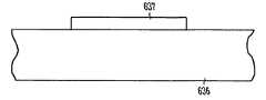
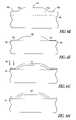
- FIG. 1Aillustrates a known device for improved hole mobility with an n-type silicon substrate 101 , a silicon germanium layer 102 , a silicon capping layer 103 , a gate oxide 104 , a gate 105 , and N+ source/drain regions 106 and 107 .
- FIG. 1Billustrates a band structure for the device of FIG. 1A , and indicates that some carriers or holes are at the silicon-oxide interface and some are confined in the silicon germanium layer. Both the silicon germanium and the silicon capping layers will be strained if they are thin. Alternatively, the silicon germanium layer may be graded to a relaxed or unstrained layer resulting in more stress in the silicon cap layer. The crystalline silicon layer is strained by a lattice mismatch between the silicon germanium layer and the crystalline silicon layer.
- strained silicon layershave been fabricated on thicker relaxed silicon germanium layers to improve the mobility of electrons in NMOS transistors. Structures with strained silicon on silicon germanium on insulators have been described as well as structures with strained silicon over a localized oxide insulator region. These structures yield high mobility and high performance transistors on a low capacitance insulating substrate.
- Wafer bendinghas been used to investigate the effect of strain on mobility and distinguish between the effects of biaxial stress and uniaxial stress. Bonding a semiconductor onto bowed or bent substrates has been disclosed to introduce strain in the semiconductor. Stress can also be introduced by wafer bonding. Packaging can introduce mechanical stress by bending. Compressively-strained semiconductor layers have been bonded to a substrate.
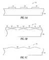
- FIGS. 2-4illustrate some known techniques to strain channels and improve carrier mobilities in CMOS devices.
- FIG. 2illustrates a known device design to improve electron mobility in NMOS transistors using a tensile strained silicon layer on silicon germanium.
- a graded silicon germanium layer 208is formed on a p-type silicon substrate 209 to provide a relaxed silicon germanium region 210 , upon which a strained silicon layer 211 is grown.
- the transistor channelis formed in the strained silicon layer 211 .
- uniaxial compressive stresscan be introduced in a channel 312 of a PMOS transistor to improve hole mobility using silicon germanium source/drain regions 313 in trenches adjacent to the PMOS transistor.
- Silicon-carbide source/drain regions in trenches adjacent to an NMOS transistorcan introduce tensile stress and improve electron mobility.
- FIG. 4illustrates a known device design to improve mobility for both NMOS and PMOS transistors using silicon nitride capping layers 414 . These silicon nitride capping layers can be formed to introduce tensile stress for NMOS transistors and can be formed to introduce compressive stress for PMOS transistors.
- FIG. 1Aillustrates a known device for improved hole mobility
- FIG. 1Billustrates a band structure for the device of FIG. 1A .
- FIG. 2illustrates a known device design to improve electron mobility in NMOS transistors using a tensile strained silicon layer on silicon germanium.
- FIG. 3illustrates a known device design to provide uniaxial compressive stress in a channel of a PMOS transistor using silicon germanium source/drain regions in trenches adjacent to the PMOS transistor.
- FIG. 4illustrates a known device design to improve mobility for both NMOS and PMOS transistors using silicon nitride capping layers.
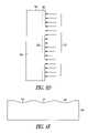
- FIGS. 5A-5Iillustrate an embodiment where a semiconductor layer is bonded to tensile strain the semiconductor layer.
- FIGS. 6A-6Killustrate an embodiment where a semiconductor layer is bonded to compressive strain the semiconductor layer.
- FIG. 7illustrates a top view of a structure in which a plurality of transistors are being formed, according to various embodiments.
- FIGS. 8-14illustrate various methods for straining semiconductor layers.
- FIG. 15is a simplified block diagram of a high-level organization of a memory device according to various embodiments.
- FIG. 16illustrates a diagram for an electronic system having one or more transistors with strained channels for improved mobility, according to various embodiments.
- FIG. 17illustrates an embodiment of a system having a controller and a memory, according to various embodiments.
- Both termsinclude doped and undoped semiconductors, epitaxial layers of a semiconductor on a supporting semiconductor or insulating material, combinations of such layers, as well as other such structures that are known in the art.
- the term “horizontal” as used in this applicationis defined as a plane parallel to the conventional plane or surface of a wafer or substrate, regardless of the orientation of the wafer or substrate.
- the term “vertical”refers to a direction perpendicular to the horizontal as defined above. Prepositions, such as “on”, “side”, “higher”, “lower”, “over” and “under” are defined with respect to the conventional plane or surface being on the top surface of the wafer or substrate, regardless of the orientation of the wafer or substrate.
- a semiconductor layeris oriented to a substrate.
- the semiconductor layerhas a surface orientation and is oriented to the substrate to provide a desired direction of conductance for the surface orientation.
- the oriented semiconductor layeris bonded to the substrate to strain the semiconductor layer.
- a strained semiconductor layeris formed on a substrate, which includes orienting a semiconductor layer to a substrate and bonding the oriented semiconductor layer to the substrate to strain the semiconductor layer.
- the semiconductor layerhas a surface orientation and is oriented to provide a desired direction of conductance for the surface orientation.
- a gate insulatoris formed on the strained semiconductor layer, a gate is formed on the gate insulator, and first and second diffusion regions define a channel beneath the gate insulator between the first and second diffusion regions.
- a strained semiconductor layeris formed on a substrate.
- a first semiconductor layer and a second semiconductor layerare oriented to a substrate.
- the first semiconductor layerhas a first surface orientation and is oriented to provide a first desired direction of conductance for the first surface orientation to promote electron mobility.
- the second semiconductor layerhas a second surface orientation and is oriented to provide a second desired direction of conductance for the second surface orientation to promote hole mobility.
- the first and second oriented semiconductor layersare bonded to the substrate to strain the semiconductor layer.
- An n-channel transistoris formed using the first semiconductor layer and a p-channel transistor is formed using the second semiconductor layer.
- Various structure embodimentsinclude a substrate and a crystalline semiconductor layer bonded to the substrate.
- the semiconductor layerhas a surface orientation and a desired channel conductance direction for the surface orientation.
- the crystalline semiconductor layerhas a local strained region.
- the structurefurther includes a gate oxide over the local strained region, a gate over the gate oxide, and first and second source/drain regions to provide a channel region with the desired channel conductance direction within in the local strained region.
- strips of silicon of different surface orientations and strip directionscan be bonded onto silicon substrates of various surface orientations.
- the strip directioncorresponds to a desired direction of conduction.
- the desired direction of conduction for the strained siliconis the channel direction.
- the strips of siliconcan be locally strained, and can either be tensile strained during the bonding process to improve the electron mobility and/or can be compressive strained during the bonding process to improve the hole mobility.
- the improved carrier mobilityimproves CMOS transistor performance.
- the carrier wafer or substratecan be a silicon wafer of any surface orientation, such as the common (100), (110) or (111) silicon substrates.
- FIGS. 5A-5Iillustrate an embodiment where a semiconductor layer is bonded to tensile strain the semiconductor layer, such as is provided in U.S. Published Patent Application 20040224480, filed May 7, 2003 and entitled “Micromechanical Strained Semiconductor By Wafer Bonding.”
- U.S. 20040224480is incorporated by reference herein in its entirety.
- FIGS. 5A-5Cillustrate a process for forming recesses in a substrate using a LOCal Oxidation of Silicon (LOCOS) process according to various embodiments.
- LOCOSLOCal Oxidation of Silicon
- the LOCOS processis useful to form recesses in silicon substrates, and one of ordinary skill in the art will understand, upon reading and comprehending this disclosure, that other methods to form recesses in substrates can be used for silicon and other substrates.
- FIG. 5Aillustrates a semiconductor structure 515 toward the beginning of a LOCOS process.
- the semiconductor structure 515includes a silicon substrate 516 .
- a layer of silicon nitride 517is deposited, such as by Chemical Vapor Deposition (CVD) and the like, on the silicon substrate and is etched to expose portions of the silicon substrate for subsequent selective oxidation.
- CVDChemical Vapor Deposition
- One of ordinary skill in the artwill understand, upon reading and comprehending this disclosure, that the pattern of the silicon nitride affects the pattern and characteristics of the recesses and thus of the strained semiconductor film.
- FIG. 5Billustrates the semiconductor structure 515 after the silicon substrate 516 has been oxidized.
- the oxide 518is thermally grown by means of wet oxidation. The oxide grows where there is no masking nitride. At the edges of the nitride, some oxidant diffuses laterally to grow under the nitride edges. This lateral growth has the shape of a slowly tapering oxide wedge and is commonly referred to as a “bird's beak.”
- FIG. 5Cillustrates the semiconductor structure 516 after the oxide has been removed. Recesses 519 remain where the oxidation occurred. Because of the formation of the recesses 519 , the substrate 516 , also referred to as a first wafer, can be referred to as a dimpled substrate as, in various embodiments, the substrate has a dimpled appearance. As provided below, a second wafer, or membrane, is bonded to the substrate such that portions of the second wafer are strained in the recesses of the substrate.
- LOCOS processis a common economical semiconductor fabrication process.
- Another benefit of the LOCOS processis the tapered bird's beak, which allows for controlled strain in the film.
- the slowly tapering shape of the bird's beakis useful to controllably induce strain in ultra-thin semiconductor films.
- the tapered bird's beak shapeis not required to practice the present subject matter.
- other means for creating a recess or void in the substratecan be used. For example, a grinding process can be used to create a recess or a trench can be otherwise formed in the substrate.
- FIGS. 6D-6Hillustrate a method to form a strained semiconductor membrane using a bond cut process to bond a membrane to a substrate with recesses, according to various embodiments.
- the bond cut processinvolves bonding together two substrates, or wafers, and breaking off a section of at least one of the two substrate after the substrates have been bonded together.
- the substrateis also referred to herein in various embodiments as a first wafer or dimpled substrate, and the membrane is also referred to herein in various embodiments as a second wafer.
- FIG. 5Dillustrates a sacrificial semiconductor wafer 520
- FIG. 5Eillustrates a semiconductor substrate 516
- the substrate 516includes a semiconductor material, and includes a number of recesses 519 , such as illustrated in FIG. 5C .
- the semiconductor materialincludes one of the following materials: silicon; germanium; silicon-germanium; gallium arsenide; indium phosphide; and other semiconductor materials. This list of potential semiconductor materials is not intended to be an all-inclusive list.
- the substrateis cut into wafer size patterns, and integrated circuits are formed thereon.
- the sacrificial waferincludes various semiconductor material including but not limited to silicon, germanium, silicon-germanium, gallium arsenide, indium phosphide, and other semiconductor materials.
- the sacrificial wafer 520is a single crystal wafer, and is conditioned by implanting ions 521 into a surface.
- the ionsare implanted along a plane, represented in FIG. 5D as a line 522 , to define a surface layer 523 with a predetermined thickness.
- the planeis approximately parallel to the surface in which the ions are implanted.
- hydrogen ionsare used as implantation ions.
- the hydrogen ionscan include H + , H 2 + , D + , and/or D 2 + ions.
- the implanted ionsact to form cavities along the plane 522 .
- the cavitiesare joined through thermal processing, allowing the surface layer 523 to be removed from the remaining portion of the sacrificial wafer 524 at the cleavage plane 522 .
- this thermal processingoccurs while the surface layer 523 is being bonded to the substrate 516 , as shown in FIG. 5F .
- the surface layerbreaks off of the sacrificial wafer at the cleavage plane and remains bonded to the substrate.
- the remaining portion of the sacrificial wafer 524can be used to form membranes for other substrates, thus reducing the overall cost for the manufacturing process of a wide variety of electronic devices.
- FIG. 5Fillustrates the surface layer 523 of the sacrificial wafer 520 bonded to the substrate 516 .
- the bonding forceincludes the strong Van der Waal's force that naturally bonds surfaces together as the bonding force.
- the Van der Waal's forceprovides an initial bonding force that is strengthened during subsequent thermal processing.
- the surface layer 523 of the sacrificial wafer 520is bonded to the substrate 516 in an environment 525 A at a first pressure.
- the first pressureis a vacuum or a low pressure near a vacuum.
- the bonded wafersare heated to further bond the surface layer to the substrate and to cut the surface layer 523 from the sacrificial wafer.
- the environment 525 Ahas a bonding temperature within a range of approximately 300° C. to 400° C. Heating the sacrificial wafer joins the cavities in the cleavage plane 522 , allowing the remaining portion 524 of the sacrificial wafer to be removed from the surface layer, which remains bonded to the substrate. The remaining portion 524 of the sacrificial wafer can be prepared and conditioned for another bond cut process.
- the thickness of the surface layer 523 bonded to the substrate 516is defined by the depth of ion implantation 521 during the bond cut process. In various embodiments, the thickness of the surface layer 523 is such that it does not yield or otherwise plastically deform under the desired mechanical strain induced by the bond. In various embodiments, the thickness of the surface layer 523 is less than 200 nm, such that it can be termed an ultra thin wafer. In various embodiments, the silicon layer has a thickness of about 0.1 microns (100 nm or 1000 ⁇ ). In various embodiments, the silicon layer has a thickness less than 0.1 microns. In various embodiments, the silicon layer has a thickness in a range of approximately 300 ⁇ to 1000 ⁇ .
- the silicon filmis prepared for transistor fabrication.
- the preparation of the filmincludes grinding, polishing, chemical etch, chemical etch with etch stops, and/or plasma assisted chemical etch, and the like, which can be used to further thin the film.
- the membrane bonded to the substrate illustrated in FIG. 5Gcan be thinner than the surface layer defined in the sacrificial layer in FIG. 5D .
- Device processingcan be accomplished using conventional processes and procedures.
- FIG. 5Hillustrates the membrane 523 further bonded to the substrate 516 in the recesses 519 formed therein.
- the processis performed in an environment 525 B having a second temperature.
- the second pressureis greater than the first pressure to force the membrane into the recesses.
- the volume between the membrane and the recessed substrateis a sealed volume, such that the pressure inside these volumes is approximately the first pressure.
- the second pressureis atmospheric pressure.
- the environment 525 Bhas a bonding temperature within a range of approximately 800° C. to 1000° C.
- the portion of the membrane bonded to the substrate in the recessesis strained.
- the recessescan be made with appropriate dimension to provide a desired tensile strain.
- FIG. 51illustrates a transistor fabricated with a strained semiconductor membrane, according to various embodiments.
- the illustrated transistor 530includes a crystalline semiconductor substrate 516 with a recess 519 , and a crystalline semiconductor membrane 523 bonded to the substrate 516 to provide the membrane 523 with a desired tensile strain in the recesses.
- a gate dielectric 531is formed on the strained membrane, and a gate 532 is formed on the gate dielectric 531 .
- First and second diffusion regions 533 and 534are formed in the structure 530 .
- the tensile strained semiconductor membrane 523 between the first and second diffusion regions 533 and 534forms a tensile strained channel region 535 .
- tensile strain a thin semiconductor layersuch as a silicon layer
- a strain greater than 0.5%to achieve significant mobility enhancement.
- various embodiments tensile strain a thin semiconductor wafersuch as an ultra-thin silicon wafer with a thickness within a range of approximately 300 ⁇ to 1000 ⁇ , with a strain within a range of approximately 0.75% to approximately 1.5%.
- tensile strain a thin semiconductor layersuch as a thin silicon layer, with a strain in the range of approximately 1% to approximately 1.2% to reduce unnecessary strain and provide a margin of error without unduly affecting mobility enhancement.
- the filmis approximately 1000 ⁇ or less.
- the channel length of the transistoris less than or equal to about 1000 ⁇
- the thickness of the filmis less than or equal to about 300 ⁇ . The strain enhances mobility in the channel, thus overcoming problems associated with heavy channel doping.
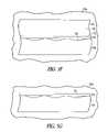
- FIGS. 6A-6Killustrate an embodiment where a semiconductor layer is bonded to compressive strain the semiconductor layer, such as is provided in U.S. patent application Ser. No. 11/356,335, filed Feb. 16, 2006 and entitled “Localized Compressive Strained Semiconductor.”
- U.S. patent application Ser. No. 11/356,335is incorporated by reference herein in its entirety.
- the description that followsrefers to embodiments with silicon and silicon dioxide or oxide. However, those of ordinary skill in the art will understand how to implement the teachings herein with other semiconductors and insulators.
- FIG. 6Aillustrates a crystalline silicon substrate 636 with a mask layer 637 .
- the mask layeris patterned to define the areas where there will be localized compressive strain. Thus, the defined areas are used to provide a channel with compressive strain to improve hole mobility for p-channel transistors.
- the maskis a silicon nitride.
- a thin native oxideis between the silicon nitride and the crystalline silicon substrate.
- the exposed crystalline silicon 636is etched at 638 to a desired depth on each side of the mask 637 .
- a thick oxide layer 639is deposited.
- the resulting structureis planarized, such as may be performed by a chemical mechanical planarization (CMP) process.
- CMPchemical mechanical planarization
- the planarizing processstops on the raised silicon areas 640 to leave islands or strips of silicon 640 embedded in an oxide 639 , such as is illustrated in the side view of FIG. 6C and the top view of FIG. 6D .
- FIG. 6Eillustrates the structure after an oxidation process.
- the dotted line 641corresponds to the top surface 641 of the structure illustrated in FIG. 6C
- the dotted lines 642correspond to the edges 642 of the oxide islands in FIG. 6C .
- the exposed silicon island 640 oxidesrapidly, while the regions covered by the deposited oxide 639 oxidize much more slowly.
- the thickness of the deposited oxide and the subsequent oxidationis timed to leave the resulting silicon surface planar under the oxides of different thickness, and to provide the desired strain, as will be evident upon reading and comprehending this specification.
- FIG. 6Fillustrates the structure after the oxide is etched back to expose the crystalline substrate 643 and reduce the oxide in the island portion 640 of the oxide.
- a “bird's beak”is left at the edges of the oxide islands.
- the bird's beakhas a similar shape to that formed by a LOCal Oxidation of Silicon (LOCOS) process.
- LOCOSLOCal Oxidation of Silicon
- a native oxide 644forms on the exposed silicon areas by exposure to air, water or peroxide.
- FIGS. 6G-6Hillustrate methods for providing an amorphous silicon layer in contact with the crystalline silicon on one side of the oxide island, according to various embodiments.
- an amorphous silicon layer 645is deposited, and a silicon implant 646 breaks up the oxide such that the crystalline silicon substrate at 647 is able to seed the crystalline growth of the amorphous silicon layer.
- the native oxideis removed at 647 from one side of the oxide island and amorphous silicon 645 is deposited and patterned over the oxide islands.
- the thickness of the silicon filmis within a range from approximately 100 nm to approximately 200 nm. Such thicknesses are capable of being mechanically compressed without affecting yield.
- FIG. 61illustrates a recrystallization process for the amorphous silicon layer, and further illustrates the bonding of the crystallized layer after the oxide island is removed.
- the recrystallization processis also referred to as a solid phase epitaxial (SPE) process, which includes depositing a thin amorphous silicon layer and annealing the structure to recrystallize the amorphous silicon, where one end of the amorphous layer is seeded to promote a desired crystalline growth.
- the recrystallizationas illustrated by the arrows 648 , is seeded at 647 where the silicon layer 645 is in direct contact with the crystalline silicon substrate 636 , and thus only grows from one side since the other side still has the unperturbed native oxide 643 .
- the silicon filmis recrystallized at temperatures from approximately 550° C. to approximately 700° C.
- the transistor channelis formed in this recrystallized silicon strip.
- the oxide islandis etched from underneath the silicon strip to leave an empty space beneath the silicon strip.
- a silicon strip or silicon bridge layeris influenced toward and bonded to the surface beneath the silicon layer.
- the naturally occurring Van der Waal's forceis sufficient to influence the bridge layer or film 645 into contact with the surface 650 beneath the silicon layer.
- a nano-imprint maskis used to assist with influencing the film into contact with the surface beneath the silicon layer.
- FIG. 6Jillustrates the silicon layer bonded to the surface beneath the silicon layer. Since the length of the bowed silicon film strip is longer than the planar surface region of the silicon substrate, the film 645 , now in crystalline form, will be under compressive stress, as illustrated by the arrows 651 , after bonding to the substrate surface.
- FIG. 6Killustrates a PMOS transistor 652 fabricated in the structure formed with crystalline silicon under compression.
- the remaining steps in the PMOS transistor fabricationcan be achieved by conventional techniques, in which the compressively-strained ultra-thin silicon strip 645 forms the transistor channel region.
- a gate insulator 653such as silicon oxide or other gate insulator, is formed on the structure
- a gate 654is formed on the gate insulator
- source/drain regions 655are formed to define a channel 645 beneath the gate and between the source/drain regions.
- the source/drain regionscan be formed by an ion implantation process.
- FIG. 7illustrates a top view of a structure in which a plurality of transistors are being formed, according to various embodiments.
- the oxide 756is illustrated by the dotted line and the pattern of silicon strips 757 is also illustrated.
- a number of oxide regionsare combined in the column direction to form one oxide area.
- the column of oxide regions 756 A- 756 Ecan be formed as one oxide area.
- these oxide areascan be used to provide a local tensile strain to the silicon strips or a local compressive strain to the silicon strips.
- the same substrateincludes silicon strips with both locally tensile strained regions to promote electron mobility and locally compressive strained regions to promote hole mobility.
- FIGS. 8-13illustrate various methods for straining semiconductor layers.
- a semiconductor layeris oriented to a substrate to provide a desired direction of conductance of a surface orientation of the semiconductor layer.
- the stripsare formed in the direction of conductance.
- Other embodimentsuse larger membranes or films.
- the surface crystal orientationis conventionally provided using Miller indices in parentheses.
- the direction of conductionis provided using X Y Z coordinates in angle brackets, and is based on the same coordinate system used to identify the surface orientation of the semiconductor layer. For a given surface crystal orientation, some directions are more conductive than others.
- the oriented semiconductor layeris bonded to the substrate to strain the semiconductor layer.
- Various embodimentsinduce a compressive strain and various embodiments induce a tensile strain when the layer is bonded to the substrate.
- the thickness of the layeris sufficiently thin to permit the strain without yield.
- Various embodimentscreate the layer using a bond cut process, such as illustrated in FIGS. 5D-5G .
- Various embodimentsremove the back of a sacrificial wafer, which has been bonded to the substrate, by a mechanical and chemical etch procedure.
- Various embodimentscreate the layer by depositing an amorphous layer and recrystallizing the layer using a solid phase epitaxial process, such as illustrated in FIGS. 6G-I .
- FIG. 9illustrates an embodiment of a method of bonding a (100) silicon layer to provide desired conductance in the ⁇ 110> direction.
- the stripsare formed in the ⁇ 110> direction.
- a (100) silicon layeris oriented to a substrate to provide a ⁇ 110> direction of conductance for the (100) silicon layer.
- the oriented (100) silicon layeris bonded to the substrate to strain the silicon layer.
- Various embodimentsbond the layer onto raised oxide areas on any carrier wafer to improve hole mobility by removing the oxide from under the strips and completing the bonding to leave the strip in compressive stress.
- Various embodimentsbond the silicon layer over recessed oxide areas on any carrier wafer to improve electron mobility by removing the oxide from under the strips and completing the bonding to leave the strip in tensile stress.
- FIG. 10illustrates an embodiment of a method of bonding a (110) silicon layer to provide desired conductance in the ⁇ 100> direction. Other directions of conductance can be used with respect to the (110) silicon layer. In embodiments in which strips of silicon are bonded to the substrate, the strips are formed in the ⁇ 100> direction.
- a (110) silicon layeris oriented to a substrate to provide a ⁇ 100> direction of conductance for the (110) silicon layer.
- the oriented (110) silicon layeris bonded to the substrate to strain the silicon layer.
- Various embodimentsbond the layer onto raised oxide areas on any carrier wafer to improve hole mobility by removing the oxide from under the strips and completing the bonding to leave the strip in compressive stress.
- Various embodimentsbond the silicon layer over recessed oxide areas on any carrier wafer to improve electron mobility by removing the oxide from under the strips and completing the bonding to leave the strip in tensile stress.
- FIG. 11illustrates an embodiment of a method of bonding a (111) silicon layer to provide desired conductance in the ⁇ 110> direction.
- the stripsare formed in the ⁇ 110> direction.
- a (111) silicon layeris oriented to a substrate to provide a ⁇ 110> direction of conductance for the (111) silicon layer.
- the oriented (111) silicon layeris bonded to the substrate to strain the silicon layer.
- the layer onto raised oxide areas on any carrier waferto improve hole mobility by removing the oxide from under the strips and completing the bonding to leave the strip in compressive stress.
- Various embodimentsbond the silicon layer over recessed oxide areas on any carrier wafer to improve electron mobility by removing the oxide from under the strips and completing the bonding to leave the strip in tensile stress.
- FIG. 12illustrates an embodiment of a method of bonding (100) silicon layers to provide desired conductance in the ⁇ 110> direction.
- a first (100) silicon layeris oriented to a substrate to provide a ⁇ 110> direction of conductance of the first (100) silicon layer, and the first (100) silicon layer is bonded to the substrate to tensile strain the first silicon layer.
- a second (100) silicon layeris oriented to a substrate to provide a ⁇ 110> direction of conductance of the first (100) silicon layer, and the second (100) silicon layer is bonded to the substrate to compressive strain the second silicon layer.
- the strips with local tensile stressimprove the mobility of n-channel MOSFETs and the strips with local compressive stress improve hole mobility of p-channel MOSFETs.
- the present subject mattercan be implemented in CMOS design.
- FIG. 13illustrates an embodiment of a method of bonding a (100) silicon layer to provide a desired conductance in the ⁇ 110> direction and bonding a (110) silicon layer to provide a desired conductance in the ⁇ 100> direction.
- a (100) silicon layeris oriented to a substrate to provide a ⁇ 110> direction of conductance and a (110) silicon layer is oriented to the substrate to provide a ⁇ 100> direction of conductance.
- the oriented (100) silicon layer and the oriented (110) silicon layerare bonded to the substrate to strain the semiconductor layers. Local strain for either the (100) layer or the (110) layer can be either tensile strain or compressive strain.
- the stripswill all have the same height above the smooth surface of the carrier wafer the backs of the strips can also be mechanically polished as well as chemically polished. Removing the oxide from under the strips and completing the bonding will leave the strips in tensile stress improving the mobility of both electrons and holes in MOSFETs.
- the MOSFETscan be fabricated using conventional techniques.
- the direction of a uniaxial straincan affect the carrier mobility.
- a ⁇ 110> channel direction and a tensile strain direction in the ⁇ 110> directionis desirable for improved electron mobility in a (100) silicon layer and a ⁇ 100> channel direction and a tensile strain in the ⁇ 100> direction is desirable for improved hole mobility in a (110) silicon layer.
- various embodimentsuniaxially strain the semiconductor layer in a desired direction with respect to the desired direction for conduction to improve carrier mobility.
- a semiconductor layeris oriented to a substrate to provide a desired direction of conductance for a surface orientation of the semiconductor layer.
- the oriented semiconductor layeris bonded to the substrate to strain the semiconductor layer.
- the bonding processincludes uniaxially straining the semiconductor layer in a desired direction with respect to the desired direction of conduction to improve conductance.
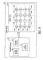
- FIG. 15is a simplified block diagram of a high-level organization of various embodiments of a memory device according to various embodiments of the present subject matter.
- the illustrated memory device 1561includes a memory array 1562 and read/write control circuitry 1563 to perform operations on the memory array via communication line(s) or channel(s) 1564 .
- the illustrated memory device 1561may be a memory card or a memory module such as a single inline memory module (SIMM) and dual inline memory module (DIMM).
- SIMMsingle inline memory module
- DIMMdual inline memory module
- semiconductor components in the memory array and/or the control circuitryare able to be fabricated using the strained semiconductor, as described above.
- the memory array and/or the control circuitryinclude p-channel transistors with improved hole mobility and/or n-channel transistors with improved electron mobility, as disclosed herein. The structure and fabrication methods for these devices have been described above.
- the illustrated memory array 1562includes a number of memory cells 1565 arranged in rows and columns, where word lines 1566 connect the memory cells in the rows and bit lines 1567 connect the memory cells in the columns.
- the read/write control circuitry 1563includes word line select circuitry 1568 , which functions to select a desired row.
- the read/write control circuitry 1563further includes bit line select circuitry 1569 , which functions to select a desired column.
- the read/write control circuitry 1563further includes read circuitry 1570 , which functions to detect a memory state for a selected memory cell in the memory array 1562 .
- FIG. 16illustrates a diagram for an electronic system having one or more transistors with strained channels for improved mobility, according to various embodiments of the present subject matter.
- Electronic system 1671includes a controller 1672 , a bus 1673 , and an electronic device 1674 , where the bus 1673 provides communication channels between the controller 1672 and the electronic device 1674 .
- the controller and/or electronic deviceinclude p-channel transistors with improved hole mobility and/or n-channel transistors with improved electron mobility, as disclosed herein.
- the illustrated electronic system 1671may include, but is not limited to, information handling devices, wireless systems, telecommunication systems, fiber optic systems, electrooptic systems, and computers.
- FIG. 17illustrates an embodiment of a system 1775 having a controller 1776 and a memory 1777 , according to various embodiments of the present subject matter.
- the controller 1776 and/or memory 1777may include p-channel transistors with improved hole mobility and/or n-channel transistors with improved electron mobility, as disclosed herein.
- the illustrated system 1775also includes an electronic apparatus 1778 and a bus 1779 to provide communication channel(s) between the controller and the electronic apparatus, and between the controller and the memory.
- the busmay include an address, a data bus, and a control bus, each independently configured; or may use common communication channels to provide address, data, and/or control, the use of which is regulated by the controller.
- the electronic apparatus 1778may be additional memory configured similar to memory 1777 .
- An embodimentmay include a peripheral device or devices 1780 coupled to the bus 1779 .
- Peripheral devicesmay include displays, additional storage memory, or other control devices that may operate in conjunction with the controller and/or the memory.
- the controlleris a processor. Any of the controller 1776 , the memory 1777 , the electronic apparatus 1778 , and the peripheral devices 1780 may include p-channel transistors with improved hole mobility and/or n-channel transistors with improved electron mobility, as disclosed herein.
- the system 1775may include, but is not limited to, information handling devices, telecommunication systems, and computers.
- Applications containing strained semiconductor films as described in this disclosureinclude electronic systems for use in memory modules, device drivers, power modules, communication modems, processor modules, and application-specific modules, and may include multilayer, multichip modules.
- Such circuitrycan further be a subcomponent of a variety of electronic systems, such as cameras, video recorders and players, televisions, displays, games, phones, clocks, personal computers, wireless devices, automobiles, aircrafts, industrial control systems, and others.
- the memorymay be realized as a memory device containing p-channel transistors with improved hole mobility and/or n-channel transistors with improved electron mobility, as disclosed herein. It will be understood that embodiments are equally applicable to any size and type of memory circuit and are not intended to be limited to a particular type of memory device.
- Memory typesinclude a DRAM, SRAM (Static Random Access Memory) or Flash memories. Additionally, the DRAM could be a synchronous DRAM commonly referred to as SGRAM (Synchronous Graphics Random Access Memory), SDRAM (Synchronous Dynamic Random Access Memory), SDRAM II, and DDR SDRAM (Double Data Rate SDRAM).
Landscapes
- Thin Film Transistor (AREA)
- Recrystallisation Techniques (AREA)
- Metal-Oxide And Bipolar Metal-Oxide Semiconductor Integrated Circuits (AREA)
- Insulated Gate Type Field-Effect Transistor (AREA)
- Chemical & Material Sciences (AREA)
- Crystallography & Structural Chemistry (AREA)
Abstract
Description
- This disclosure relates generally to semiconductor structures, and more particularly, to strained semiconductor, devices and systems, and methods of forming the strained semiconductor, devices and systems.
- The semiconductor industry continues to strive for improvements in the speed and performance of semiconductor devices. Strained silicon technology has been shown to enhance carrier mobility in both n-channel and p-channel devices, and thus has been of interest to the semiconductor industry as a means to improve device speed and performance. Currently, strained silicon layers are used to increase electron mobility in n-channel CMOS transistors. There has been research and development activity to increase the hole mobility of p-channel CMOS transistors using strained silicon germanium layers on silicon.
FIG. 1A illustrates a known device for improved hole mobility with an n-type silicon substrate 101, asilicon germanium layer 102, asilicon capping layer 103, agate oxide 104, agate 105, and N+ source/drain regions FIG. 1B illustrates a band structure for the device ofFIG. 1A , and indicates that some carriers or holes are at the silicon-oxide interface and some are confined in the silicon germanium layer. Both the silicon germanium and the silicon capping layers will be strained if they are thin. Alternatively, the silicon germanium layer may be graded to a relaxed or unstrained layer resulting in more stress in the silicon cap layer. The crystalline silicon layer is strained by a lattice mismatch between the silicon germanium layer and the crystalline silicon layer.- More recently, strained silicon layers have been fabricated on thicker relaxed silicon germanium layers to improve the mobility of electrons in NMOS transistors. Structures with strained silicon on silicon germanium on insulators have been described as well as structures with strained silicon over a localized oxide insulator region. These structures yield high mobility and high performance transistors on a low capacitance insulating substrate.
- Wafer bending has been used to investigate the effect of strain on mobility and distinguish between the effects of biaxial stress and uniaxial stress. Bonding a semiconductor onto bowed or bent substrates has been disclosed to introduce strain in the semiconductor. Stress can also be introduced by wafer bonding. Packaging can introduce mechanical stress by bending. Compressively-strained semiconductor layers have been bonded to a substrate.
FIGS. 2-4 illustrate some known techniques to strain channels and improve carrier mobilities in CMOS devices.FIG. 2 illustrates a known device design to improve electron mobility in NMOS transistors using a tensile strained silicon layer on silicon germanium. As illustrated, a gradedsilicon germanium layer 208 is formed on a p-type silicon substrate 209 to provide a relaxedsilicon germanium region 210, upon which astrained silicon layer 211 is grown. The transistor channel is formed in thestrained silicon layer 211. There is a large mismatch in the cell structure between the silicon and silicon germanium layers, which biaxially strains the silicon layer. As illustrated inFIG. 3 , uniaxial compressive stress can be introduced in achannel 312 of a PMOS transistor to improve hole mobility using silicon germanium source/drain regions 313 in trenches adjacent to the PMOS transistor. Large improvements in hole mobility, up to 50%, have been made in PMOS devices in silicon technology using strained silicon germanium source/drain regions to compressively strain the transistor channel. Silicon-carbide source/drain regions in trenches adjacent to an NMOS transistor can introduce tensile stress and improve electron mobility.FIG. 4 illustrates a known device design to improve mobility for both NMOS and PMOS transistors using siliconnitride capping layers 414. These silicon nitride capping layers can be formed to introduce tensile stress for NMOS transistors and can be formed to introduce compressive stress for PMOS transistors.- Another proposal to improve device speed and performance involves higher mobility surfaces. For example, it has been proposed to bond unstrained (110) layers of silicon onto (100) surface substrates to improve hole mobility in unstrained channel regions of p-channel MOSFETs, and to amorphize the regions in which to fabricate n-channel transistors and recrystallize the (100) silicon seeded by the underlying (100) substrate to provide the unstrained channel region of n-channel MOSFETs with the high channel mobility characteristic of the (100) surface.
FIG. 1A illustrates a known device for improved hole mobility, andFIG. 1B illustrates a band structure for the device ofFIG. 1A .FIG. 2 illustrates a known device design to improve electron mobility in NMOS transistors using a tensile strained silicon layer on silicon germanium.FIG. 3 illustrates a known device design to provide uniaxial compressive stress in a channel of a PMOS transistor using silicon germanium source/drain regions in trenches adjacent to the PMOS transistor.FIG. 4 illustrates a known device design to improve mobility for both NMOS and PMOS transistors using silicon nitride capping layers.FIGS. 5A-5I illustrate an embodiment where a semiconductor layer is bonded to tensile strain the semiconductor layer.FIGS. 6A-6K illustrate an embodiment where a semiconductor layer is bonded to compressive strain the semiconductor layer.FIG. 7 illustrates a top view of a structure in which a plurality of transistors are being formed, according to various embodiments.FIGS. 8-14 illustrate various methods for straining semiconductor layers.FIG. 15 is a simplified block diagram of a high-level organization of a memory device according to various embodiments.FIG. 16 illustrates a diagram for an electronic system having one or more transistors with strained channels for improved mobility, according to various embodiments.FIG. 17 illustrates an embodiment of a system having a controller and a memory, according to various embodiments.- The following detailed description refers to the accompanying drawings which show, by way of illustration, specific aspects and embodiments in which the present subject matter may be practiced. These embodiments are described in sufficient detail to enable those skilled in the art to practice the present subject matter. The various embodiments of the present subject matter are not necessarily mutually exclusive as aspects of one embodiment can be combined with aspects of another embodiment. Other embodiments may be utilized and structural, logical, and electrical changes may be made without departing from the scope of the present subject matter. In the following description, the terms “wafer” and “substrate” are interchangeably used to refer generally to any structure on which integrated circuits are formed, and also to such structures during various stages of integrated circuit fabrication. Both terms include doped and undoped semiconductors, epitaxial layers of a semiconductor on a supporting semiconductor or insulating material, combinations of such layers, as well as other such structures that are known in the art. The term “horizontal” as used in this application is defined as a plane parallel to the conventional plane or surface of a wafer or substrate, regardless of the orientation of the wafer or substrate. The term “vertical” refers to a direction perpendicular to the horizontal as defined above. Prepositions, such as “on”, “side”, “higher”, “lower”, “over” and “under” are defined with respect to the conventional plane or surface being on the top surface of the wafer or substrate, regardless of the orientation of the wafer or substrate. The following detailed description is, therefore, not to be taken in a limiting sense, and the scope of the present invention is defined only by the appended claims, along with the full scope of equivalents to which such claims are entitled.
- According to various method embodiments, a semiconductor layer is oriented to a substrate. The semiconductor layer has a surface orientation and is oriented to the substrate to provide a desired direction of conductance for the surface orientation. The oriented semiconductor layer is bonded to the substrate to strain the semiconductor layer.
- According to various embodiments for forming a transistor, a strained semiconductor layer is formed on a substrate, which includes orienting a semiconductor layer to a substrate and bonding the oriented semiconductor layer to the substrate to strain the semiconductor layer. The semiconductor layer has a surface orientation and is oriented to provide a desired direction of conductance for the surface orientation. A gate insulator is formed on the strained semiconductor layer, a gate is formed on the gate insulator, and first and second diffusion regions define a channel beneath the gate insulator between the first and second diffusion regions.
- According to various embodiments for forming a CMOS device, a strained semiconductor layer is formed on a substrate. A first semiconductor layer and a second semiconductor layer are oriented to a substrate. The first semiconductor layer has a first surface orientation and is oriented to provide a first desired direction of conductance for the first surface orientation to promote electron mobility. The second semiconductor layer has a second surface orientation and is oriented to provide a second desired direction of conductance for the second surface orientation to promote hole mobility. The first and second oriented semiconductor layers are bonded to the substrate to strain the semiconductor layer. An n-channel transistor is formed using the first semiconductor layer and a p-channel transistor is formed using the second semiconductor layer.
- Various structure embodiments include a substrate and a crystalline semiconductor layer bonded to the substrate. The semiconductor layer has a surface orientation and a desired channel conductance direction for the surface orientation. The crystalline semiconductor layer has a local strained region. The structure further includes a gate oxide over the local strained region, a gate over the gate oxide, and first and second source/drain regions to provide a channel region with the desired channel conductance direction within in the local strained region.
- For example, strips of silicon of different surface orientations and strip directions can be bonded onto silicon substrates of various surface orientations. The strip direction corresponds to a desired direction of conduction. In transistor embodiments, the desired direction of conduction for the strained silicon is the channel direction. The strips of silicon can be locally strained, and can either be tensile strained during the bonding process to improve the electron mobility and/or can be compressive strained during the bonding process to improve the hole mobility. The improved carrier mobility improves CMOS transistor performance. The carrier wafer or substrate can be a silicon wafer of any surface orientation, such as the common (100), (110) or (111) silicon substrates.
FIGS. 5A-5I illustrate an embodiment where a semiconductor layer is bonded to tensile strain the semiconductor layer, such as is provided in U.S. Published Patent Application 20040224480, filed May 7, 2003 and entitled “Micromechanical Strained Semiconductor By Wafer Bonding.” U.S. 20040224480 is incorporated by reference herein in its entirety.FIGS. 5A-5C illustrate a process for forming recesses in a substrate using a LOCal Oxidation of Silicon (LOCOS) process according to various embodiments. The LOCOS process is useful to form recesses in silicon substrates, and one of ordinary skill in the art will understand, upon reading and comprehending this disclosure, that other methods to form recesses in substrates can be used for silicon and other substrates.FIG. 5A illustrates asemiconductor structure 515 toward the beginning of a LOCOS process. Thesemiconductor structure 515 includes asilicon substrate 516. A layer ofsilicon nitride 517 is deposited, such as by Chemical Vapor Deposition (CVD) and the like, on the silicon substrate and is etched to expose portions of the silicon substrate for subsequent selective oxidation. One of ordinary skill in the art will understand, upon reading and comprehending this disclosure, that the pattern of the silicon nitride affects the pattern and characteristics of the recesses and thus of the strained semiconductor film.FIG. 5B illustrates thesemiconductor structure 515 after thesilicon substrate 516 has been oxidized. In various embodiments, theoxide 518 is thermally grown by means of wet oxidation. The oxide grows where there is no masking nitride. At the edges of the nitride, some oxidant diffuses laterally to grow under the nitride edges. This lateral growth has the shape of a slowly tapering oxide wedge and is commonly referred to as a “bird's beak.”FIG. 5C illustrates thesemiconductor structure 516 after the oxide has been removed.Recesses 519 remain where the oxidation occurred. Because of the formation of therecesses 519, thesubstrate 516, also referred to as a first wafer, can be referred to as a dimpled substrate as, in various embodiments, the substrate has a dimpled appearance. As provided below, a second wafer, or membrane, is bonded to the substrate such that portions of the second wafer are strained in the recesses of the substrate.- One benefit of the LOCOS process is that it is a common economical semiconductor fabrication process. Another benefit of the LOCOS process is the tapered bird's beak, which allows for controlled strain in the film. One of ordinary skill in the art will understand, upon reading and comprehending this disclosure, that the slowly tapering shape of the bird's beak is useful to controllably induce strain in ultra-thin semiconductor films. However, the tapered bird's beak shape is not required to practice the present subject matter. One of ordinary skill in the art will understand, upon reading and comprehending this disclosure, that other means for creating a recess or void in the substrate can be used. For example, a grinding process can be used to create a recess or a trench can be otherwise formed in the substrate.
FIGS. 6D-6H illustrate a method to form a strained semiconductor membrane using a bond cut process to bond a membrane to a substrate with recesses, according to various embodiments. The bond cut process involves bonding together two substrates, or wafers, and breaking off a section of at least one of the two substrate after the substrates have been bonded together. The substrate is also referred to herein in various embodiments as a first wafer or dimpled substrate, and the membrane is also referred to herein in various embodiments as a second wafer.FIG. 5D illustrates asacrificial semiconductor wafer 520, andFIG. 5E illustrates asemiconductor substrate 516. Thesubstrate 516 includes a semiconductor material, and includes a number ofrecesses 519, such as illustrated inFIG. 5C . In various embodiments, the semiconductor material includes one of the following materials: silicon; germanium; silicon-germanium; gallium arsenide; indium phosphide; and other semiconductor materials. This list of potential semiconductor materials is not intended to be an all-inclusive list. The substrate is cut into wafer size patterns, and integrated circuits are formed thereon. In various embodiments, the sacrificial wafer includes various semiconductor material including but not limited to silicon, germanium, silicon-germanium, gallium arsenide, indium phosphide, and other semiconductor materials.- The
sacrificial wafer 520 is a single crystal wafer, and is conditioned by implantingions 521 into a surface. The ions are implanted along a plane, represented inFIG. 5D as aline 522, to define asurface layer 523 with a predetermined thickness. The plane is approximately parallel to the surface in which the ions are implanted. In various embodiments, hydrogen ions are used as implantation ions. The hydrogen ions can include H+, H2+, D+, and/or D2+ ions. The implanted ions act to form cavities along theplane 522. The cavities are joined through thermal processing, allowing thesurface layer 523 to be removed from the remaining portion of thesacrificial wafer 524 at thecleavage plane 522. In various embodiments, this thermal processing occurs while thesurface layer 523 is being bonded to thesubstrate 516, as shown inFIG. 5F . Once these cavities join and the surface layer is bonded to the substrate, the surface layer breaks off of the sacrificial wafer at the cleavage plane and remains bonded to the substrate. The remaining portion of thesacrificial wafer 524 can be used to form membranes for other substrates, thus reducing the overall cost for the manufacturing process of a wide variety of electronic devices. FIG. 5F illustrates thesurface layer 523 of thesacrificial wafer 520 bonded to thesubstrate 516. Before the surface layer is bonded to the substrate, the sacrificial wafer and the substrate can be cleaned using conventional cleaning procedures. In various embodiments, the bonding force includes the strong Van der Waal's force that naturally bonds surfaces together as the bonding force. In various embodiments, the Van der Waal's force provides an initial bonding force that is strengthened during subsequent thermal processing. As illustrated inFIG. 5F , thesurface layer 523 of thesacrificial wafer 520 is bonded to thesubstrate 516 in anenvironment 525A at a first pressure. In various embodiments, the first pressure is a vacuum or a low pressure near a vacuum.- In various embodiments, the bonded wafers are heated to further bond the surface layer to the substrate and to cut the
surface layer 523 from the sacrificial wafer. In various embodiments, theenvironment 525A has a bonding temperature within a range of approximately 300° C. to 400° C. Heating the sacrificial wafer joins the cavities in thecleavage plane 522, allowing the remainingportion 524 of the sacrificial wafer to be removed from the surface layer, which remains bonded to the substrate. The remainingportion 524 of the sacrificial wafer can be prepared and conditioned for another bond cut process. - The thickness of the
surface layer 523 bonded to thesubstrate 516 is defined by the depth ofion implantation 521 during the bond cut process. In various embodiments, the thickness of thesurface layer 523 is such that it does not yield or otherwise plastically deform under the desired mechanical strain induced by the bond. In various embodiments, the thickness of thesurface layer 523 is less than 200 nm, such that it can be termed an ultra thin wafer. In various embodiments, the silicon layer has a thickness of about 0.1 microns (100 nm or 1000 Å). In various embodiments, the silicon layer has a thickness less than 0.1 microns. In various embodiments, the silicon layer has a thickness in a range of approximately 300 Å to 1000 Å. - In various embodiments, the silicon film is prepared for transistor fabrication. In various embodiments, the preparation of the film includes grinding, polishing, chemical etch, chemical etch with etch stops, and/or plasma assisted chemical etch, and the like, which can be used to further thin the film. Thus, the membrane bonded to the substrate illustrated in
FIG. 5G can be thinner than the surface layer defined in the sacrificial layer inFIG. 5D . Device processing can be accomplished using conventional processes and procedures. FIG. 5H illustrates themembrane 523 further bonded to thesubstrate 516 in therecesses 519 formed therein. The process is performed in anenvironment 525B having a second temperature. The second pressure is greater than the first pressure to force the membrane into the recesses. The volume between the membrane and the recessed substrate is a sealed volume, such that the pressure inside these volumes is approximately the first pressure. In various embodiments, the second pressure is atmospheric pressure. In various embodiments, theenvironment 525B has a bonding temperature within a range of approximately 800° C. to 1000° C. The portion of the membrane bonded to the substrate in the recesses is strained. One of ordinary skill in the art will understand, upon reading and comprehending this disclosure, that the recesses can be made with appropriate dimension to provide a desired tensile strain.FIG. 51 illustrates a transistor fabricated with a strained semiconductor membrane, according to various embodiments. The illustratedtransistor 530 includes acrystalline semiconductor substrate 516 with arecess 519, and acrystalline semiconductor membrane 523 bonded to thesubstrate 516 to provide themembrane 523 with a desired tensile strain in the recesses. Agate dielectric 531 is formed on the strained membrane, and agate 532 is formed on thegate dielectric 531. First andsecond diffusion regions structure 530. The tensilestrained semiconductor membrane 523 between the first andsecond diffusion regions strained channel region 535.- Various embodiments tensile strain a thin semiconductor layer, such as a silicon layer, with a strain greater than 0.5% to achieve significant mobility enhancement. For further mobility enhancement, various embodiments tensile strain a thin semiconductor wafer, such as an ultra-thin silicon wafer with a thickness within a range of approximately 300 Å to 1000 Å, with a strain within a range of approximately 0.75% to approximately 1.5%. Various embodiments tensile strain a thin semiconductor layer, such as a thin silicon layer, with a strain in the range of approximately 1% to approximately 1.2% to reduce unnecessary strain and provide a margin of error without unduly affecting mobility enhancement. In various embodiments, the film is approximately 1000 Å or less. In various embodiments, the channel length of the transistor is less than or equal to about 1000 Å, and the thickness of the film is less than or equal to about 300 Å. The strain enhances mobility in the channel, thus overcoming problems associated with heavy channel doping.
FIGS. 6A-6K illustrate an embodiment where a semiconductor layer is bonded to compressive strain the semiconductor layer, such as is provided in U.S. patent application Ser. No. 11/356,335, filed Feb. 16, 2006 and entitled “Localized Compressive Strained Semiconductor.” U.S. patent application Ser. No. 11/356,335 is incorporated by reference herein in its entirety. The description that follows refers to embodiments with silicon and silicon dioxide or oxide. However, those of ordinary skill in the art will understand how to implement the teachings herein with other semiconductors and insulators.FIG. 6A illustrates acrystalline silicon substrate 636 with amask layer 637. The mask layer is patterned to define the areas where there will be localized compressive strain. Thus, the defined areas are used to provide a channel with compressive strain to improve hole mobility for p-channel transistors. In various embodiments, the mask is a silicon nitride. A thin native oxide is between the silicon nitride and the crystalline silicon substrate.- As illustrated in
FIG. 6B , the exposedcrystalline silicon 636 is etched at638 to a desired depth on each side of themask 637. Athick oxide layer 639 is deposited. The resulting structure is planarized, such as may be performed by a chemical mechanical planarization (CMP) process. The planarizing process stops on the raisedsilicon areas 640 to leave islands or strips ofsilicon 640 embedded in anoxide 639, such as is illustrated in the side view ofFIG. 6C and the top view ofFIG. 6D . FIG. 6E illustrates the structure after an oxidation process. The dottedline 641 corresponds to thetop surface 641 of the structure illustrated inFIG. 6C , and thedotted lines 642 correspond to theedges 642 of the oxide islands inFIG. 6C . The exposedsilicon island 640 oxides rapidly, while the regions covered by the depositedoxide 639 oxidize much more slowly. The thickness of the deposited oxide and the subsequent oxidation is timed to leave the resulting silicon surface planar under the oxides of different thickness, and to provide the desired strain, as will be evident upon reading and comprehending this specification.FIG. 6F illustrates the structure after the oxide is etched back to expose thecrystalline substrate 643 and reduce the oxide in theisland portion 640 of the oxide. A “bird's beak” is left at the edges of the oxide islands. The bird's beak has a similar shape to that formed by a LOCal Oxidation of Silicon (LOCOS) process. Anative oxide 644 forms on the exposed silicon areas by exposure to air, water or peroxide.FIGS. 6G-6H illustrate methods for providing an amorphous silicon layer in contact with the crystalline silicon on one side of the oxide island, according to various embodiments. As illustrated inFIG. 6G , anamorphous silicon layer 645 is deposited, and asilicon implant 646 breaks up the oxide such that the crystalline silicon substrate at647 is able to seed the crystalline growth of the amorphous silicon layer. As illustrated inFIG. 6H , the native oxide is removed at647 from one side of the oxide island andamorphous silicon 645 is deposited and patterned over the oxide islands. According to various embodiments, the thickness of the silicon film is within a range from approximately 100 nm to approximately 200 nm. Such thicknesses are capable of being mechanically compressed without affecting yield.FIG. 61 illustrates a recrystallization process for the amorphous silicon layer, and further illustrates the bonding of the crystallized layer after the oxide island is removed. The recrystallization process is also referred to as a solid phase epitaxial (SPE) process, which includes depositing a thin amorphous silicon layer and annealing the structure to recrystallize the amorphous silicon, where one end of the amorphous layer is seeded to promote a desired crystalline growth. The recrystallization, as illustrated by thearrows 648, is seeded at647 where thesilicon layer 645 is in direct contact with thecrystalline silicon substrate 636, and thus only grows from one side since the other side still has the unperturbednative oxide 643. According to various embodiments, the silicon film is recrystallized at temperatures from approximately 550° C. to approximately 700° C. The transistor channel is formed in this recrystallized silicon strip. The oxide island is etched from underneath the silicon strip to leave an empty space beneath the silicon strip. As illustrated by thearrow 649, a silicon strip or silicon bridge layer is influenced toward and bonded to the surface beneath the silicon layer. In various embodiments, the naturally occurring Van der Waal's force is sufficient to influence the bridge layer orfilm 645 into contact with thesurface 650 beneath the silicon layer. In various embodiments, a nano-imprint mask is used to assist with influencing the film into contact with the surface beneath the silicon layer.FIG. 6J illustrates the silicon layer bonded to the surface beneath the silicon layer. Since the length of the bowed silicon film strip is longer than the planar surface region of the silicon substrate, thefilm 645, now in crystalline form, will be under compressive stress, as illustrated by thearrows 651, after bonding to the substrate surface.FIG. 6K illustrates aPMOS transistor 652 fabricated in the structure formed with crystalline silicon under compression. The remaining steps in the PMOS transistor fabrication can be achieved by conventional techniques, in which the compressively-strainedultra-thin silicon strip 645 forms the transistor channel region. For example, agate insulator 653, such as silicon oxide or other gate insulator, is formed on the structure, agate 654 is formed on the gate insulator, and source/drain regions 655 are formed to define achannel 645 beneath the gate and between the source/drain regions. The source/drain regions can be formed by an ion implantation process.FIG. 7 illustrates a top view of a structure in which a plurality of transistors are being formed, according to various embodiments. Theoxide 756 is illustrated by the dotted line and the pattern of silicon strips757 is also illustrated. In another embodiment, a number of oxide regions are combined in the column direction to form one oxide area. For example, the column ofoxide regions 756A-756E can be formed as one oxide area. As discussed above, these oxide areas can be used to provide a local tensile strain to the silicon strips or a local compressive strain to the silicon strips. According to various embodiments, the same substrate includes silicon strips with both locally tensile strained regions to promote electron mobility and locally compressive strained regions to promote hole mobility.FIGS. 8-13 illustrate various methods for straining semiconductor layers. With reference to the embodiment illustrated inFIG. 8 , as illustrated at858 a semiconductor layer is oriented to a substrate to provide a desired direction of conductance of a surface orientation of the semiconductor layer. In embodiments in which strips of semiconductor are bonded to the substrate, the strips are formed in the direction of conductance. Other embodiments use larger membranes or films. The surface crystal orientation is conventionally provided using Miller indices in parentheses. The direction of conduction is provided using X Y Z coordinates in angle brackets, and is based on the same coordinate system used to identify the surface orientation of the semiconductor layer. For a given surface crystal orientation, some directions are more conductive than others. At859, the oriented semiconductor layer is bonded to the substrate to strain the semiconductor layer. Various embodiments induce a compressive strain and various embodiments induce a tensile strain when the layer is bonded to the substrate. The thickness of the layer is sufficiently thin to permit the strain without yield. Various embodiments create the layer using a bond cut process, such as illustrated inFIGS. 5D-5G . Various embodiments remove the back of a sacrificial wafer, which has been bonded to the substrate, by a mechanical and chemical etch procedure. Various embodiments create the layer by depositing an amorphous layer and recrystallizing the layer using a solid phase epitaxial process, such as illustrated inFIGS. 6G-I .FIG. 9 illustrates an embodiment of a method of bonding a (100) silicon layer to provide desired conductance in the <110> direction. In embodiments in which strips of silicon are bonded to the substrate, the strips are formed in the <110> direction. At958, a (100) silicon layer is oriented to a substrate to provide a <110> direction of conductance for the (100) silicon layer. At959, the oriented (100) silicon layer is bonded to the substrate to strain the silicon layer. Various embodiments bond the layer onto raised oxide areas on any carrier wafer to improve hole mobility by removing the oxide from under the strips and completing the bonding to leave the strip in compressive stress. Various embodiments bond the silicon layer over recessed oxide areas on any carrier wafer to improve electron mobility by removing the oxide from under the strips and completing the bonding to leave the strip in tensile stress.FIG. 10 illustrates an embodiment of a method of bonding a (110) silicon layer to provide desired conductance in the <100> direction. Other directions of conductance can be used with respect to the (110) silicon layer. In embodiments in which strips of silicon are bonded to the substrate, the strips are formed in the <100> direction. At1058, a (110) silicon layer is oriented to a substrate to provide a <100> direction of conductance for the (110) silicon layer. At1059, the oriented (110) silicon layer is bonded to the substrate to strain the silicon layer. Various embodiments bond the layer onto raised oxide areas on any carrier wafer to improve hole mobility by removing the oxide from under the strips and completing the bonding to leave the strip in compressive stress. Various embodiments bond the silicon layer over recessed oxide areas on any carrier wafer to improve electron mobility by removing the oxide from under the strips and completing the bonding to leave the strip in tensile stress.FIG. 11 illustrates an embodiment of a method of bonding a (111) silicon layer to provide desired conductance in the <110> direction. In embodiments in which strips of silicon are bonded to the substrate, the strips are formed in the <110> direction. At1158, a (111) silicon layer is oriented to a substrate to provide a <110> direction of conductance for the (111) silicon layer. At1159, the oriented (111) silicon layer is bonded to the substrate to strain the silicon layer. Various embodiments bond the layer onto raised oxide areas on any carrier wafer to improve hole mobility by removing the oxide from under the strips and completing the bonding to leave the strip in compressive stress. Various embodiments bond the silicon layer over recessed oxide areas on any carrier wafer to improve electron mobility by removing the oxide from under the strips and completing the bonding to leave the strip in tensile stress.FIG. 12 illustrates an embodiment of a method of bonding (100) silicon layers to provide desired conductance in the <110> direction. As illustrated at1258A and1259A, a first (100) silicon layer is oriented to a substrate to provide a <110> direction of conductance of the first (100) silicon layer, and the first (100) silicon layer is bonded to the substrate to tensile strain the first silicon layer. As illustrated in1258B and1259B, a second (100) silicon layer is oriented to a substrate to provide a <110> direction of conductance of the first (100) silicon layer, and the second (100) silicon layer is bonded to the substrate to compressive strain the second silicon layer. Thus, on a same substrate, the strips with local tensile stress improve the mobility of n-channel MOSFETs and the strips with local compressive stress improve hole mobility of p-channel MOSFETs. Thus, the present subject matter can be implemented in CMOS design.FIG. 13 illustrates an embodiment of a method of bonding a (100) silicon layer to provide a desired conductance in the <110> direction and bonding a (110) silicon layer to provide a desired conductance in the <100> direction. At1358, a (100) silicon layer is oriented to a substrate to provide a <110> direction of conductance and a (110) silicon layer is oriented to the substrate to provide a <100> direction of conductance. At1359, the oriented (100) silicon layer and the oriented (110) silicon layer are bonded to the substrate to strain the semiconductor layers. Local strain for either the (100) layer or the (110) layer can be either tensile strain or compressive strain. Since in this case the strips will all have the same height above the smooth surface of the carrier wafer the backs of the strips can also be mechanically polished as well as chemically polished. Removing the oxide from under the strips and completing the bonding will leave the strips in tensile stress improving the mobility of both electrons and holes in MOSFETs. The MOSFETs can be fabricated using conventional techniques.- The direction of a uniaxial strain can affect the carrier mobility. For example, as reported by Irie et al., “In-Plane Mobility Anisotropy and Universality Under Uni-Axial Strains In N- and P-MOS Inversion Layers On (100), (110), and (111) Si,” IEDM Technical Digest, 13-15 Dec. 2004, pp. 224-228, a <110> channel direction and a tensile strain direction in the <110> direction is desirable for improved electron mobility in a (100) silicon layer and a <100> channel direction and a tensile strain in the <100> direction is desirable for improved hole mobility in a (110) silicon layer. Thus, various embodiments uniaxially strain the semiconductor layer in a desired direction with respect to the desired direction for conduction to improve carrier mobility. With reference to
FIG. 14 , at1458 a semiconductor layer is oriented to a substrate to provide a desired direction of conductance for a surface orientation of the semiconductor layer. At1459 the oriented semiconductor layer is bonded to the substrate to strain the semiconductor layer. As illustrated by1460, the bonding process includes uniaxially straining the semiconductor layer in a desired direction with respect to the desired direction of conduction to improve conductance. FIG. 15 is a simplified block diagram of a high-level organization of various embodiments of a memory device according to various embodiments of the present subject matter. The illustratedmemory device 1561 includes amemory array 1562 and read/write control circuitry 1563 to perform operations on the memory array via communication line(s) or channel(s)1564. The illustratedmemory device 1561 may be a memory card or a memory module such as a single inline memory module (SIMM) and dual inline memory module (DIMM). One of ordinary skill in the art will understand, upon reading and comprehending this disclosure, that semiconductor components in the memory array and/or the control circuitry are able to be fabricated using the strained semiconductor, as described above. For example, in various embodiments, the memory array and/or the control circuitry include p-channel transistors with improved hole mobility and/or n-channel transistors with improved electron mobility, as disclosed herein. The structure and fabrication methods for these devices have been described above.- The illustrated
memory array 1562 includes a number ofmemory cells 1565 arranged in rows and columns, whereword lines 1566 connect the memory cells in the rows andbit lines 1567 connect the memory cells in the columns. The read/write control circuitry 1563 includes word lineselect circuitry 1568, which functions to select a desired row. The read/write control circuitry 1563 further includes bit lineselect circuitry 1569, which functions to select a desired column. The read/write control circuitry 1563 further includes readcircuitry 1570, which functions to detect a memory state for a selected memory cell in thememory array 1562. FIG. 16 illustrates a diagram for an electronic system having one or more transistors with strained channels for improved mobility, according to various embodiments of the present subject matter.Electronic system 1671 includes acontroller 1672, abus 1673, and an electronic device1674, where thebus 1673 provides communication channels between thecontroller 1672 and the electronic device1674. In various embodiments, the controller and/or electronic device include p-channel transistors with improved hole mobility and/or n-channel transistors with improved electron mobility, as disclosed herein. The illustratedelectronic system 1671 may include, but is not limited to, information handling devices, wireless systems, telecommunication systems, fiber optic systems, electrooptic systems, and computers.FIG. 17 illustrates an embodiment of asystem 1775 having acontroller 1776 and amemory 1777, according to various embodiments of the present subject matter. Thecontroller 1776 and/ormemory 1777 may include p-channel transistors with improved hole mobility and/or n-channel transistors with improved electron mobility, as disclosed herein. The illustratedsystem 1775 also includes anelectronic apparatus 1778 and abus 1779 to provide communication channel(s) between the controller and the electronic apparatus, and between the controller and the memory. The bus may include an address, a data bus, and a control bus, each independently configured; or may use common communication channels to provide address, data, and/or control, the use of which is regulated by the controller. In an embodiment, theelectronic apparatus 1778 may be additional memory configured similar tomemory 1777. An embodiment may include a peripheral device ordevices 1780 coupled to thebus 1779. Peripheral devices may include displays, additional storage memory, or other control devices that may operate in conjunction with the controller and/or the memory. In an embodiment, the controller is a processor. Any of thecontroller 1776, thememory 1777, theelectronic apparatus 1778, and theperipheral devices 1780 may include p-channel transistors with improved hole mobility and/or n-channel transistors with improved electron mobility, as disclosed herein. Thesystem 1775 may include, but is not limited to, information handling devices, telecommunication systems, and computers. Applications containing strained semiconductor films as described in this disclosure include electronic systems for use in memory modules, device drivers, power modules, communication modems, processor modules, and application-specific modules, and may include multilayer, multichip modules. Such circuitry can further be a subcomponent of a variety of electronic systems, such as cameras, video recorders and players, televisions, displays, games, phones, clocks, personal computers, wireless devices, automobiles, aircrafts, industrial control systems, and others.- The memory may be realized as a memory device containing p-channel transistors with improved hole mobility and/or n-channel transistors with improved electron mobility, as disclosed herein. It will be understood that embodiments are equally applicable to any size and type of memory circuit and are not intended to be limited to a particular type of memory device. Memory types include a DRAM, SRAM (Static Random Access Memory) or Flash memories. Additionally, the DRAM could be a synchronous DRAM commonly referred to as SGRAM (Synchronous Graphics Random Access Memory), SDRAM (Synchronous Dynamic Random Access Memory), SDRAM II, and DDR SDRAM (Double Data Rate SDRAM).
- This disclosure includes several processes, circuit diagrams, and semiconductor structures. The present subject matter is not limited to a particular process order or logical arrangement. Although specific embodiments have been illustrated and described herein, it will be appreciated by those of ordinary skill in the art that any arrangement which is calculated to achieve the same purpose may be substituted for the specific embodiments shown. This application is intended to cover adaptations or variations of the present subject matter. It is to be understood that the above description is intended to be illustrative, and not restrictive. Combinations of the above embodiments, and other embodiments, will be apparent to those of skill in the art upon reviewing the above description. The scope of the present subject matter should be determined with reference to the appended claims, along with the full scope of equivalents to which such claims are entitled.
Claims (67)
Priority Applications (2)
| Application Number | Priority Date | Filing Date | Title |
|---|---|---|---|
| US11/498,586US8962447B2 (en) | 2006-08-03 | 2006-08-03 | Bonded strained semiconductor with a desired surface orientation and conductance direction |
| US14/628,825US20150171165A1 (en) | 2006-08-03 | 2015-02-23 | Bonded strained semiconductor with a desired surface orientation and conductance direction |
Applications Claiming Priority (1)
| Application Number | Priority Date | Filing Date | Title |
|---|---|---|---|
| US11/498,586US8962447B2 (en) | 2006-08-03 | 2006-08-03 | Bonded strained semiconductor with a desired surface orientation and conductance direction |
Related Child Applications (1)
| Application Number | Title | Priority Date | Filing Date |
|---|---|---|---|
| US14/628,825ContinuationUS20150171165A1 (en) | 2006-08-03 | 2015-02-23 | Bonded strained semiconductor with a desired surface orientation and conductance direction |
Publications (2)
| Publication Number | Publication Date |
|---|---|
| US20080029832A1true US20080029832A1 (en) | 2008-02-07 |
| US8962447B2 US8962447B2 (en) | 2015-02-24 |
Family
ID=39028319
Family Applications (2)
| Application Number | Title | Priority Date | Filing Date |
|---|---|---|---|
| US11/498,586Active2027-01-27US8962447B2 (en) | 2006-08-03 | 2006-08-03 | Bonded strained semiconductor with a desired surface orientation and conductance direction |
| US14/628,825AbandonedUS20150171165A1 (en) | 2006-08-03 | 2015-02-23 | Bonded strained semiconductor with a desired surface orientation and conductance direction |
Family Applications After (1)
| Application Number | Title | Priority Date | Filing Date |
|---|---|---|---|
| US14/628,825AbandonedUS20150171165A1 (en) | 2006-08-03 | 2015-02-23 | Bonded strained semiconductor with a desired surface orientation and conductance direction |
Country Status (1)
| Country | Link |
|---|---|
| US (2) | US8962447B2 (en) |
Cited By (7)
| Publication number | Priority date | Publication date | Assignee | Title |
|---|---|---|---|---|
| US20070187683A1 (en)* | 2006-02-16 | 2007-08-16 | Micron Technology, Inc. | Localized compressive strained semiconductor |
| US7482190B2 (en) | 2003-05-07 | 2009-01-27 | Micron Technology, Inc. | Micromechanical strained semiconductor by wafer bonding |
| US20100216297A1 (en)* | 2007-03-23 | 2010-08-26 | Micron Technology, Inc. | Methods for fabricating semiconductor device structures |
| US20130062710A1 (en)* | 2011-09-12 | 2013-03-14 | Infineon Technologies Ag | Micro Electrical Mechanical System with Bending Deflection of Backplate Structure |
| US8679928B2 (en) | 2007-05-08 | 2014-03-25 | Micron Technology, Inc. | Methods for stressing transistor channels of a semiconductor device structure |
| US20170092809A1 (en)* | 2015-09-30 | 2017-03-30 | Commissariat A I'energie Atomique Et Aux Energies Alternatives | Method for forming a semiconducting portion by epitaxial growth on a strained portion |
| US20170093130A1 (en)* | 2015-09-30 | 2017-03-30 | Commissariat A I'energie Atomique Et Aux Energies Alternatives | Method of production of a semiconducting structure comprising a strained portion |
Families Citing this family (4)
| Publication number | Priority date | Publication date | Assignee | Title |
|---|---|---|---|---|
| US9165945B1 (en)* | 2014-09-18 | 2015-10-20 | Soitec | Method for fabricating semiconductor structures including transistor channels having different strain states, and related semiconductor structures |
| US9209301B1 (en) | 2014-09-18 | 2015-12-08 | Soitec | Method for fabricating semiconductor layers including transistor channels having different strain states, and related semiconductor layers |
| US9219150B1 (en) | 2014-09-18 | 2015-12-22 | Soitec | Method for fabricating semiconductor structures including fin structures with different strain states, and related semiconductor structures |
| US9793398B1 (en) | 2016-08-02 | 2017-10-17 | International Business Machines Corporation | Fabrication of a strained region on a substrate |
Citations (60)
| Publication number | Priority date | Publication date | Assignee | Title |
|---|---|---|---|---|
| US5234535A (en)* | 1992-12-10 | 1993-08-10 | International Business Machines Corporation | Method of producing a thin silicon-on-insulator layer |
| US5441591A (en)* | 1993-06-07 | 1995-08-15 | The United States Of America As Represented By The Secretary Of The Navy | Silicon to sapphire bond |
| US5461243A (en)* | 1993-10-29 | 1995-10-24 | International Business Machines Corporation | Substrate for tensilely strained semiconductor |
| US5877070A (en)* | 1997-05-31 | 1999-03-02 | Max-Planck Society | Method for the transfer of thin layers of monocrystalline material to a desirable substrate |
| US5879996A (en)* | 1996-09-18 | 1999-03-09 | Micron Technology, Inc. | Silicon-germanium devices for CMOS formed by ion implantation and solid phase epitaxial regrowth |
| US5963817A (en)* | 1997-10-16 | 1999-10-05 | International Business Machines Corporation | Bulk and strained silicon on insulator using local selective oxidation |
| US6049106A (en)* | 1999-01-14 | 2000-04-11 | Micron Technology, Inc. | Large grain single crystal vertical thin film polysilicon MOSFETs |
| US6228694B1 (en)* | 1999-06-28 | 2001-05-08 | Intel Corporation | Method of increasing the mobility of MOS transistors by use of localized stress regions |
| US6238796B1 (en)* | 1998-02-17 | 2001-05-29 | Seagate Technology Llc | Magnetic recording media |
| US6245615B1 (en)* | 1999-08-31 | 2001-06-12 | Micron Technology, Inc. | Method and apparatus on (110) surfaces of silicon structures with conduction in the <110> direction |
| US6309950B1 (en)* | 1998-08-04 | 2001-10-30 | Micron Technology, Inc. | Methods for making silicon-on-insulator structures |
| US6319784B1 (en)* | 1999-05-26 | 2001-11-20 | Taiwan Semiconductor Manufacturing Company | Using high temperature H2 anneal to recrystallize S/D and remove native oxide simultaneously |
| US20020001965A1 (en)* | 1996-09-04 | 2002-01-03 | Leonard Forbes | Technique for producing small islands of silicon on insulator |
| US6423613B1 (en)* | 1998-11-10 | 2002-07-23 | Micron Technology, Inc. | Low temperature silicon wafer bond process with bulk material bond strength |
| US6455397B1 (en)* | 1999-11-16 | 2002-09-24 | Rona E. Belford | Method of producing strained microelectronic and/or optical integrated and discrete devices |
| US6486008B1 (en)* | 2000-02-25 | 2002-11-26 | John Wolf International, Inc. | Manufacturing method of a thin film on a substrate |
| US20020185686A1 (en)* | 2001-06-12 | 2002-12-12 | International Business Machines Corporation | Relaxed SiGe layers on Si or silicon-on-insulator substrates by ion implantation and thermal annealing |
| US20030013323A1 (en)* | 2001-06-14 | 2003-01-16 | Richard Hammond | Method of selective removal of SiGe alloys |
| US6515335B1 (en)* | 2002-01-04 | 2003-02-04 | International Business Machines Corporation | Method for fabrication of relaxed SiGe buffer layers on silicon-on-insulators and structures containing the same |
| US6514836B2 (en)* | 2001-06-04 | 2003-02-04 | Rona Elizabeth Belford | Methods of producing strained microelectronic and/or optical integrated and discrete devices |
| US6603156B2 (en)* | 2001-03-31 | 2003-08-05 | International Business Machines Corporation | Strained silicon on insulator structures |
| US6649492B2 (en)* | 2002-02-11 | 2003-11-18 | International Business Machines Corporation | Strained Si based layer made by UHV-CVD, and devices therein |
| US6689671B1 (en)* | 2002-05-22 | 2004-02-10 | Advanced Micro Devices, Inc. | Low temperature solid-phase epitaxy fabrication process for MOS devices built on strained semiconductor substrate |
| US6703648B1 (en)* | 2002-10-29 | 2004-03-09 | Advanced Micro Devices, Inc. | Strained silicon PMOS having silicon germanium source/drain extensions and method for its fabrication |
| US6717216B1 (en)* | 2002-12-12 | 2004-04-06 | International Business Machines Corporation | SOI based field effect transistor having a compressive film in undercut area under the channel and a method of making the device |
| US6732940B2 (en)* | 1998-11-30 | 2004-05-11 | Vehicle Systems Incorporated | Compact vehicle heating apparatus and method |
| US6740913B2 (en)* | 1999-06-28 | 2004-05-25 | Intel Corporation | MOS transistor using mechanical stress to control short channel effects |
| US6767802B1 (en)* | 2003-09-19 | 2004-07-27 | Sharp Laboratories Of America, Inc. | Methods of making relaxed silicon-germanium on insulator via layer transfer |
| US20040173798A1 (en)* | 2003-03-05 | 2004-09-09 | Micron Technology, Inc. | Micro-mechanically strained semiconductor film |
| US6812116B2 (en)* | 2002-12-13 | 2004-11-02 | Taiwan Semiconductor Manufacturing Company, Ltd. | Method of fabricating a wafer with strained channel layers for increased electron and hole mobility for improving device performance |
| US20040217352A1 (en)* | 2003-04-29 | 2004-11-04 | Micron Technology, Inc. | Strained semiconductor by wafer bonding with misorientation |
| US20040221792A1 (en)* | 2003-05-07 | 2004-11-11 | Micron Technology, Inc. | Strained Si/SiGe structures by ion implantation |
| US20040224480A1 (en)* | 2003-05-07 | 2004-11-11 | Micron Technology, Inc. | Micromechanical strained semiconductor by wafer bonding |
| US20040232488A1 (en)* | 2003-05-21 | 2004-11-25 | Micron Technology, Inc. | Silicon oxycarbide substrates for bonded silicon on insulator |
| US20040232487A1 (en)* | 2003-05-21 | 2004-11-25 | Micron Technology, Inc. | Ultra-thin semiconductors bonded on glass substrates |
| US6828214B2 (en)* | 2001-04-06 | 2004-12-07 | Canon Kabushiki Kaisha | Semiconductor member manufacturing method and semiconductor device manufacturing method |
| US20050020094A1 (en)* | 2003-07-21 | 2005-01-27 | Micron Technology, Inc. | Strained semiconductor by full wafer bonding |
| US20050023616A1 (en)* | 2003-04-29 | 2005-02-03 | Micron Technology, Inc. | Localized strained semiconductor on insulator |
| US20050029619A1 (en)* | 2003-08-05 | 2005-02-10 | Micron Technology, Inc. | Strained Si/SiGe/SOI islands and processes of making same |
| US6881650B2 (en)* | 2001-12-03 | 2005-04-19 | Samsung Electronics Co., Ltd. | Method for forming SOI substrate |
| US6900521B2 (en)* | 2002-06-10 | 2005-05-31 | Micron Technology, Inc. | Vertical transistors and output prediction logic circuits containing same |
| US20050118754A1 (en)* | 2003-11-18 | 2005-06-02 | Silicon Genesis Corporation | Method for fabricating semiconductor devices using strained silicon bearing material |
| US6902962B2 (en)* | 2003-04-04 | 2005-06-07 | Taiwan Semiconductor Manufacturing Company, Ltd. | Silicon-on-insulator chip with multiple crystal orientations |
| US6911379B2 (en)* | 2003-03-05 | 2005-06-28 | Taiwan Semiconductor Manufacturing Company, Ltd. | Method of forming strained silicon on insulator substrate |
| US20050156210A1 (en)* | 2002-06-25 | 2005-07-21 | Amberwave Systems Corporation | Methods of forming reacted conductive gate electrodes |
| US20050184345A1 (en)* | 2003-07-25 | 2005-08-25 | Chun-Chieh Lin | Strained-channel semiconductor structure and method of fabricating the same |
| US6940089B2 (en)* | 2001-04-04 | 2005-09-06 | Massachusetts Institute Of Technology | Semiconductor device structure |
| US6963078B2 (en)* | 2003-03-15 | 2005-11-08 | International Business Machines Corporation | Dual strain-state SiGe layers for microelectronics |
| US20050247972A1 (en)* | 2004-05-06 | 2005-11-10 | Micron Technology, Inc. | Ballistic direct injection NROM cell on strained silicon structures |
| US20050259475A1 (en)* | 2004-05-18 | 2005-11-24 | Micron Technology, Inc. | Ballistic injection nrom flash memory |
| US20050276117A1 (en)* | 2004-05-26 | 2005-12-15 | Micron Technology, Inc. | Ballistic direct injection flash memory cell on strained silicon structures |
| US6987039B2 (en)* | 2001-10-03 | 2006-01-17 | Texas Instruments Incorporated | Forming lateral bipolar junction transistor in CMOS flow |
| US20060024917A1 (en)* | 2004-07-29 | 2006-02-02 | Silicon Genesis Corporation | Method and system for fabricating strained layers for the manufacture of integrated circuits |
| US20060049460A1 (en)* | 2004-05-28 | 2006-03-09 | Hung-Wei Chen | CMOS logic gate fabricated on hybrid crystal orientations and method of forming thereof |
| US20060094175A1 (en)* | 2004-11-01 | 2006-05-04 | International Business Machines Corporation | In-place bonding of microstructures |
| US20060118915A1 (en)* | 2004-12-07 | 2006-06-08 | Hwang Chul J | Semiconductor substrate, semiconductor device and method of manufacturing the same |
| US20060292822A1 (en)* | 2005-06-27 | 2006-12-28 | Ya-Hong Xie | Method for producing dislocation-free strained crystalline films |
| US20070087514A1 (en)* | 2005-04-28 | 2007-04-19 | Kabushiki Kaisha Toshiba | SOI substrate with selective oxide layer thickness control |
| US20070096170A1 (en)* | 2005-11-02 | 2007-05-03 | International Business Machines Corporation | Low modulus spacers for channel stress enhancement |
| US20070187683A1 (en)* | 2006-02-16 | 2007-08-16 | Micron Technology, Inc. | Localized compressive strained semiconductor |
Family Cites Families (3)
| Publication number | Priority date | Publication date | Assignee | Title |
|---|---|---|---|---|
| JPS54155770A (en) | 1978-05-29 | 1979-12-08 | Nec Corp | Manufacture of semiconductor device |
| US6328796B1 (en) | 1999-02-01 | 2001-12-11 | The United States Of America As Represented By The Secretary Of The Navy | Single-crystal material on non-single-crystalline substrate |
| JP3956572B2 (en) | 2000-03-13 | 2007-08-08 | セイコーエプソン株式会社 | Method for manufacturing substrate for liquid crystal device |
- 2006
- 2006-08-03USUS11/498,586patent/US8962447B2/enactiveActive
- 2015
- 2015-02-23USUS14/628,825patent/US20150171165A1/ennot_activeAbandoned
Patent Citations (81)
| Publication number | Priority date | Publication date | Assignee | Title |
|---|---|---|---|---|
| US5234535A (en)* | 1992-12-10 | 1993-08-10 | International Business Machines Corporation | Method of producing a thin silicon-on-insulator layer |
| US5441591A (en)* | 1993-06-07 | 1995-08-15 | The United States Of America As Represented By The Secretary Of The Navy | Silicon to sapphire bond |
| US5461243A (en)* | 1993-10-29 | 1995-10-24 | International Business Machines Corporation | Substrate for tensilely strained semiconductor |
| US5759898A (en)* | 1993-10-29 | 1998-06-02 | International Business Machines Corporation | Production of substrate for tensilely strained semiconductor |
| US20020001965A1 (en)* | 1996-09-04 | 2002-01-03 | Leonard Forbes | Technique for producing small islands of silicon on insulator |
| US5879996A (en)* | 1996-09-18 | 1999-03-09 | Micron Technology, Inc. | Silicon-germanium devices for CMOS formed by ion implantation and solid phase epitaxial regrowth |
| US5877070A (en)* | 1997-05-31 | 1999-03-02 | Max-Planck Society | Method for the transfer of thin layers of monocrystalline material to a desirable substrate |
| US5963817A (en)* | 1997-10-16 | 1999-10-05 | International Business Machines Corporation | Bulk and strained silicon on insulator using local selective oxidation |
| US6251751B1 (en)* | 1997-10-16 | 2001-06-26 | International Business Machines Corporation | Bulk and strained silicon on insulator using local selective oxidation |
| US6238796B1 (en)* | 1998-02-17 | 2001-05-29 | Seagate Technology Llc | Magnetic recording media |
| US6309950B1 (en)* | 1998-08-04 | 2001-10-30 | Micron Technology, Inc. | Methods for making silicon-on-insulator structures |
| US6423613B1 (en)* | 1998-11-10 | 2002-07-23 | Micron Technology, Inc. | Low temperature silicon wafer bond process with bulk material bond strength |
| US6732940B2 (en)* | 1998-11-30 | 2004-05-11 | Vehicle Systems Incorporated | Compact vehicle heating apparatus and method |
| US6049106A (en)* | 1999-01-14 | 2000-04-11 | Micron Technology, Inc. | Large grain single crystal vertical thin film polysilicon MOSFETs |
| US6319784B1 (en)* | 1999-05-26 | 2001-11-20 | Taiwan Semiconductor Manufacturing Company | Using high temperature H2 anneal to recrystallize S/D and remove native oxide simultaneously |
| US6228694B1 (en)* | 1999-06-28 | 2001-05-08 | Intel Corporation | Method of increasing the mobility of MOS transistors by use of localized stress regions |
| US6740913B2 (en)* | 1999-06-28 | 2004-05-25 | Intel Corporation | MOS transistor using mechanical stress to control short channel effects |
| US6960821B2 (en)* | 1999-08-31 | 2005-11-01 | Micron Technology, Inc. | Method and apparatus on (110) surfaces of silicon structures with conduction in the <110> direction |
| US6245615B1 (en)* | 1999-08-31 | 2001-06-12 | Micron Technology, Inc. | Method and apparatus on (110) surfaces of silicon structures with conduction in the <110> direction |
| US6455397B1 (en)* | 1999-11-16 | 2002-09-24 | Rona E. Belford | Method of producing strained microelectronic and/or optical integrated and discrete devices |
| US6486008B1 (en)* | 2000-02-25 | 2002-11-26 | John Wolf International, Inc. | Manufacturing method of a thin film on a substrate |
| US6603156B2 (en)* | 2001-03-31 | 2003-08-05 | International Business Machines Corporation | Strained silicon on insulator structures |
| US6940089B2 (en)* | 2001-04-04 | 2005-09-06 | Massachusetts Institute Of Technology | Semiconductor device structure |
| US6828214B2 (en)* | 2001-04-06 | 2004-12-07 | Canon Kabushiki Kaisha | Semiconductor member manufacturing method and semiconductor device manufacturing method |
| US6514836B2 (en)* | 2001-06-04 | 2003-02-04 | Rona Elizabeth Belford | Methods of producing strained microelectronic and/or optical integrated and discrete devices |
| US6593625B2 (en)* | 2001-06-12 | 2003-07-15 | International Business Machines Corporation | Relaxed SiGe layers on Si or silicon-on-insulator substrates by ion implantation and thermal annealing |
| US20020185686A1 (en)* | 2001-06-12 | 2002-12-12 | International Business Machines Corporation | Relaxed SiGe layers on Si or silicon-on-insulator substrates by ion implantation and thermal annealing |
| US20030201468A1 (en)* | 2001-06-12 | 2003-10-30 | Christiansen Silke H. | Relaxed SiGe layers on Si or silicon-on-insulator substrates by ion implantation and thermal annealing |
| US20030013323A1 (en)* | 2001-06-14 | 2003-01-16 | Richard Hammond | Method of selective removal of SiGe alloys |
| US6987039B2 (en)* | 2001-10-03 | 2006-01-17 | Texas Instruments Incorporated | Forming lateral bipolar junction transistor in CMOS flow |
| US6881650B2 (en)* | 2001-12-03 | 2005-04-19 | Samsung Electronics Co., Ltd. | Method for forming SOI substrate |
| US6515335B1 (en)* | 2002-01-04 | 2003-02-04 | International Business Machines Corporation | Method for fabrication of relaxed SiGe buffer layers on silicon-on-insulators and structures containing the same |
| US6649492B2 (en)* | 2002-02-11 | 2003-11-18 | International Business Machines Corporation | Strained Si based layer made by UHV-CVD, and devices therein |
| US6689671B1 (en)* | 2002-05-22 | 2004-02-10 | Advanced Micro Devices, Inc. | Low temperature solid-phase epitaxy fabrication process for MOS devices built on strained semiconductor substrate |
| US20050156230A1 (en)* | 2002-06-10 | 2005-07-21 | Leonard Forbes | Output prediction logic circuits with ultra-thin vertical transistors and methods of formation |
| US6900521B2 (en)* | 2002-06-10 | 2005-05-31 | Micron Technology, Inc. | Vertical transistors and output prediction logic circuits containing same |
| US20050156210A1 (en)* | 2002-06-25 | 2005-07-21 | Amberwave Systems Corporation | Methods of forming reacted conductive gate electrodes |
| US6703648B1 (en)* | 2002-10-29 | 2004-03-09 | Advanced Micro Devices, Inc. | Strained silicon PMOS having silicon germanium source/drain extensions and method for its fabrication |
| US6717216B1 (en)* | 2002-12-12 | 2004-04-06 | International Business Machines Corporation | SOI based field effect transistor having a compressive film in undercut area under the channel and a method of making the device |
| US6812116B2 (en)* | 2002-12-13 | 2004-11-02 | Taiwan Semiconductor Manufacturing Company, Ltd. | Method of fabricating a wafer with strained channel layers for increased electron and hole mobility for improving device performance |
| US20040173798A1 (en)* | 2003-03-05 | 2004-09-09 | Micron Technology, Inc. | Micro-mechanically strained semiconductor film |
| US6911379B2 (en)* | 2003-03-05 | 2005-06-28 | Taiwan Semiconductor Manufacturing Company, Ltd. | Method of forming strained silicon on insulator substrate |
| US6963078B2 (en)* | 2003-03-15 | 2005-11-08 | International Business Machines Corporation | Dual strain-state SiGe layers for microelectronics |
| US6902962B2 (en)* | 2003-04-04 | 2005-06-07 | Taiwan Semiconductor Manufacturing Company, Ltd. | Silicon-on-insulator chip with multiple crystal orientations |
| US20050023529A1 (en)* | 2003-04-29 | 2005-02-03 | Micron Technology, Inc. | Strained semiconductor by wafer bonding with misorientation |
| US20050023616A1 (en)* | 2003-04-29 | 2005-02-03 | Micron Technology, Inc. | Localized strained semiconductor on insulator |
| US7041575B2 (en)* | 2003-04-29 | 2006-05-09 | Micron Technology, Inc. | Localized strained semiconductor on insulator |
| US20040217352A1 (en)* | 2003-04-29 | 2004-11-04 | Micron Technology, Inc. | Strained semiconductor by wafer bonding with misorientation |
| US20040224480A1 (en)* | 2003-05-07 | 2004-11-11 | Micron Technology, Inc. | Micromechanical strained semiconductor by wafer bonding |
| US7115480B2 (en)* | 2003-05-07 | 2006-10-03 | Micron Technology, Inc. | Micromechanical strained semiconductor by wafer bonding |
| US20050032296A1 (en)* | 2003-05-07 | 2005-02-10 | Micron Technology, Inc. | Micromechanical strained semiconductor by wafer bonding |
| US6987037B2 (en)* | 2003-05-07 | 2006-01-17 | Micron Technology, Inc. | Strained Si/SiGe structures by ion implantation |
| US20040221792A1 (en)* | 2003-05-07 | 2004-11-11 | Micron Technology, Inc. | Strained Si/SiGe structures by ion implantation |
| US20050023612A1 (en)* | 2003-05-21 | 2005-02-03 | Micron Technology, Inc. | Ultra-thin semiconductors bonded on glass substrates |
| US20040232488A1 (en)* | 2003-05-21 | 2004-11-25 | Micron Technology, Inc. | Silicon oxycarbide substrates for bonded silicon on insulator |
| US20040232487A1 (en)* | 2003-05-21 | 2004-11-25 | Micron Technology, Inc. | Ultra-thin semiconductors bonded on glass substrates |
| US20050020094A1 (en)* | 2003-07-21 | 2005-01-27 | Micron Technology, Inc. | Strained semiconductor by full wafer bonding |
| US20050184345A1 (en)* | 2003-07-25 | 2005-08-25 | Chun-Chieh Lin | Strained-channel semiconductor structure and method of fabricating the same |
| US20050087842A1 (en)* | 2003-08-05 | 2005-04-28 | Micron Technology, Inc. | Strained Si/SiGe/SOI islands and processes of making same |
| US20050029619A1 (en)* | 2003-08-05 | 2005-02-10 | Micron Technology, Inc. | Strained Si/SiGe/SOI islands and processes of making same |
| US6767802B1 (en)* | 2003-09-19 | 2004-07-27 | Sharp Laboratories Of America, Inc. | Methods of making relaxed silicon-germanium on insulator via layer transfer |
| US20050118754A1 (en)* | 2003-11-18 | 2005-06-02 | Silicon Genesis Corporation | Method for fabricating semiconductor devices using strained silicon bearing material |
| US20050247972A1 (en)* | 2004-05-06 | 2005-11-10 | Micron Technology, Inc. | Ballistic direct injection NROM cell on strained silicon structures |
| US20050259475A1 (en)* | 2004-05-18 | 2005-11-24 | Micron Technology, Inc. | Ballistic injection nrom flash memory |
| US20050276117A1 (en)* | 2004-05-26 | 2005-12-15 | Micron Technology, Inc. | Ballistic direct injection flash memory cell on strained silicon structures |
| US20060049460A1 (en)* | 2004-05-28 | 2006-03-09 | Hung-Wei Chen | CMOS logic gate fabricated on hybrid crystal orientations and method of forming thereof |
| US20060024917A1 (en)* | 2004-07-29 | 2006-02-02 | Silicon Genesis Corporation | Method and system for fabricating strained layers for the manufacture of integrated circuits |
| US20060094175A1 (en)* | 2004-11-01 | 2006-05-04 | International Business Machines Corporation | In-place bonding of microstructures |
| US7238589B2 (en)* | 2004-11-01 | 2007-07-03 | International Business Machines Corporation | In-place bonding of microstructures |
| US20060118915A1 (en)* | 2004-12-07 | 2006-06-08 | Hwang Chul J | Semiconductor substrate, semiconductor device and method of manufacturing the same |
| US20070087514A1 (en)* | 2005-04-28 | 2007-04-19 | Kabushiki Kaisha Toshiba | SOI substrate with selective oxide layer thickness control |
| US20060292822A1 (en)* | 2005-06-27 | 2006-12-28 | Ya-Hong Xie | Method for producing dislocation-free strained crystalline films |
| US20070096170A1 (en)* | 2005-11-02 | 2007-05-03 | International Business Machines Corporation | Low modulus spacers for channel stress enhancement |
| US20070187683A1 (en)* | 2006-02-16 | 2007-08-16 | Micron Technology, Inc. | Localized compressive strained semiconductor |
| US7544584B2 (en)* | 2006-02-16 | 2009-06-09 | Micron Technology, Inc. | Localized compressive strained semiconductor |
| US20090218566A1 (en)* | 2006-02-16 | 2009-09-03 | Micron Technology, Inc. | Localized compressive strained semiconductor |
| US8124977B2 (en)* | 2006-02-16 | 2012-02-28 | Micron Technology, Inc. | Localized compressive strained semiconductor |
| US20120122287A1 (en)* | 2006-02-16 | 2012-05-17 | Leonard Forbes | Localized compressive strained semiconductor |
| US8227309B2 (en)* | 2006-02-16 | 2012-07-24 | Micron Technology, Inc. | Localized compressive strained semiconductor |
| US20120289016A1 (en)* | 2006-02-16 | 2012-11-15 | Leonard Forbes | Localized compressive strained semiconductor |
| US8435850B2 (en)* | 2006-02-16 | 2013-05-07 | Micron Technology, Inc. | Localized compressive strained semiconductor |
Cited By (18)
| Publication number | Priority date | Publication date | Assignee | Title |
|---|---|---|---|---|
| US7482190B2 (en) | 2003-05-07 | 2009-01-27 | Micron Technology, Inc. | Micromechanical strained semiconductor by wafer bonding |
| US8435850B2 (en) | 2006-02-16 | 2013-05-07 | Micron Technology, Inc. | Localized compressive strained semiconductor |
| US7544584B2 (en) | 2006-02-16 | 2009-06-09 | Micron Technology, Inc. | Localized compressive strained semiconductor |
| US20090218566A1 (en)* | 2006-02-16 | 2009-09-03 | Micron Technology, Inc. | Localized compressive strained semiconductor |
| US8124977B2 (en) | 2006-02-16 | 2012-02-28 | Micron Technology, Inc. | Localized compressive strained semiconductor |
| US8227309B2 (en) | 2006-02-16 | 2012-07-24 | Micron Technology, Inc. | Localized compressive strained semiconductor |
| US20070187683A1 (en)* | 2006-02-16 | 2007-08-16 | Micron Technology, Inc. | Localized compressive strained semiconductor |
| US20100216297A1 (en)* | 2007-03-23 | 2010-08-26 | Micron Technology, Inc. | Methods for fabricating semiconductor device structures |
| US7871911B2 (en) | 2007-03-23 | 2011-01-18 | Micron Technology, Inc. | Methods for fabricating semiconductor device structures |
| US9076867B2 (en) | 2007-05-08 | 2015-07-07 | Micron Technology, Inc. | Semiconductor device structures including strained transistor channels |
| US8679928B2 (en) | 2007-05-08 | 2014-03-25 | Micron Technology, Inc. | Methods for stressing transistor channels of a semiconductor device structure |
| CN103121657A (en)* | 2011-09-12 | 2013-05-29 | 英飞凌科技股份有限公司 | Micro electrical mechanical system with bending deflection of backplate structure |
| US20130062710A1 (en)* | 2011-09-12 | 2013-03-14 | Infineon Technologies Ag | Micro Electrical Mechanical System with Bending Deflection of Backplate Structure |
| US9148726B2 (en)* | 2011-09-12 | 2015-09-29 | Infineon Technologies Ag | Micro electrical mechanical system with bending deflection of backplate structure |
| US20170092809A1 (en)* | 2015-09-30 | 2017-03-30 | Commissariat A I'energie Atomique Et Aux Energies Alternatives | Method for forming a semiconducting portion by epitaxial growth on a strained portion |
| US20170093130A1 (en)* | 2015-09-30 | 2017-03-30 | Commissariat A I'energie Atomique Et Aux Energies Alternatives | Method of production of a semiconducting structure comprising a strained portion |
| US9735317B2 (en)* | 2015-09-30 | 2017-08-15 | Commissariat A L'energie Atomique Et Aux Energies Alternatives | Method for forming a semiconducting portion by epitaxial growth on a strained portion |
| US9774167B2 (en)* | 2015-09-30 | 2017-09-26 | Commissariat A L'energie Atomique Et Aux Energies Alternatives | Method of production of a semiconducting structure comprising a strained portion |
Also Published As
| Publication number | Publication date |
|---|---|
| US20150171165A1 (en) | 2015-06-18 |
| US8962447B2 (en) | 2015-02-24 |
Similar Documents
| Publication | Publication Date | Title |
|---|---|---|
| US8962447B2 (en) | Bonded strained semiconductor with a desired surface orientation and conductance direction | |
| US9379241B2 (en) | Semiconductor device with strained channels | |
| US7485544B2 (en) | Strained semiconductor, devices and systems and methods of formation | |
| KR100724560B1 (en) | Semiconductor device having crystalline semiconductor layer, manufacturing method thereof and driving method thereof | |
| US8227309B2 (en) | Localized compressive strained semiconductor | |
| US7662701B2 (en) | Gettering of silicon on insulator using relaxed silicon germanium epitaxial proximity layers | |
| US7405444B2 (en) | Micro-mechanically strained semiconductor film | |
| US7262428B2 (en) | Strained Si/SiGe/SOI islands and processes of making same | |
| US7482190B2 (en) | Micromechanical strained semiconductor by wafer bonding | |
| JP3512701B2 (en) | Semiconductor device and manufacturing method thereof | |
| US20080111190A1 (en) | Integration of a floating body memory on SOI with logic transistors on bulk substrate | |
| US7511381B2 (en) | Thin film transistor and method of manufacturing the same | |
| US20100155788A1 (en) | Formation of a multiple crystal orientation substrate | |
| JPH04206766A (en) | Manufacturing method of semiconductor device | |
| WO2022227338A1 (en) | Preparation method for semiconductor structure |
Legal Events
| Date | Code | Title | Description |
|---|---|---|---|
| AS | Assignment | Owner name:MICRON TECHNOLOGY, INC., IDAHO Free format text:ASSIGNMENT OF ASSIGNORS INTEREST;ASSIGNOR:FORBES, LEONARD;REEL/FRAME:018138/0573 Effective date:20060620 | |
| FEPP | Fee payment procedure | Free format text:PAYOR NUMBER ASSIGNED (ORIGINAL EVENT CODE: ASPN); ENTITY STATUS OF PATENT OWNER: LARGE ENTITY | |
| STCF | Information on status: patent grant | Free format text:PATENTED CASE | |
| AS | Assignment | Owner name:U.S. BANK NATIONAL ASSOCIATION, AS COLLATERAL AGENT, CALIFORNIA Free format text:SECURITY INTEREST;ASSIGNOR:MICRON TECHNOLOGY, INC.;REEL/FRAME:038669/0001 Effective date:20160426 Owner name:U.S. BANK NATIONAL ASSOCIATION, AS COLLATERAL AGEN Free format text:SECURITY INTEREST;ASSIGNOR:MICRON TECHNOLOGY, INC.;REEL/FRAME:038669/0001 Effective date:20160426 | |
| AS | Assignment | Owner name:MORGAN STANLEY SENIOR FUNDING, INC., AS COLLATERAL AGENT, MARYLAND Free format text:PATENT SECURITY AGREEMENT;ASSIGNOR:MICRON TECHNOLOGY, INC.;REEL/FRAME:038954/0001 Effective date:20160426 Owner name:MORGAN STANLEY SENIOR FUNDING, INC., AS COLLATERAL Free format text:PATENT SECURITY AGREEMENT;ASSIGNOR:MICRON TECHNOLOGY, INC.;REEL/FRAME:038954/0001 Effective date:20160426 | |
| AS | Assignment | Owner name:U.S. BANK NATIONAL ASSOCIATION, AS COLLATERAL AGENT, CALIFORNIA Free format text:CORRECTIVE ASSIGNMENT TO CORRECT THE REPLACE ERRONEOUSLY FILED PATENT #7358718 WITH THE CORRECT PATENT #7358178 PREVIOUSLY RECORDED ON REEL 038669 FRAME 0001. ASSIGNOR(S) HEREBY CONFIRMS THE SECURITY INTEREST;ASSIGNOR:MICRON TECHNOLOGY, INC.;REEL/FRAME:043079/0001 Effective date:20160426 Owner name:U.S. BANK NATIONAL ASSOCIATION, AS COLLATERAL AGEN Free format text:CORRECTIVE ASSIGNMENT TO CORRECT THE REPLACE ERRONEOUSLY FILED PATENT #7358718 WITH THE CORRECT PATENT #7358178 PREVIOUSLY RECORDED ON REEL 038669 FRAME 0001. ASSIGNOR(S) HEREBY CONFIRMS THE SECURITY INTEREST;ASSIGNOR:MICRON TECHNOLOGY, INC.;REEL/FRAME:043079/0001 Effective date:20160426 | |
| AS | Assignment | Owner name:JPMORGAN CHASE BANK, N.A., AS COLLATERAL AGENT, ILLINOIS Free format text:SECURITY INTEREST;ASSIGNORS:MICRON TECHNOLOGY, INC.;MICRON SEMICONDUCTOR PRODUCTS, INC.;REEL/FRAME:047540/0001 Effective date:20180703 Owner name:JPMORGAN CHASE BANK, N.A., AS COLLATERAL AGENT, IL Free format text:SECURITY INTEREST;ASSIGNORS:MICRON TECHNOLOGY, INC.;MICRON SEMICONDUCTOR PRODUCTS, INC.;REEL/FRAME:047540/0001 Effective date:20180703 | |
| MAFP | Maintenance fee payment | Free format text:PAYMENT OF MAINTENANCE FEE, 4TH YEAR, LARGE ENTITY (ORIGINAL EVENT CODE: M1551) Year of fee payment:4 | |
| AS | Assignment | Owner name:MICRON TECHNOLOGY, INC., IDAHO Free format text:RELEASE BY SECURED PARTY;ASSIGNOR:U.S. BANK NATIONAL ASSOCIATION, AS COLLATERAL AGENT;REEL/FRAME:047243/0001 Effective date:20180629 | |
| AS | Assignment | Owner name:MICRON TECHNOLOGY, INC., IDAHO Free format text:RELEASE BY SECURED PARTY;ASSIGNOR:MORGAN STANLEY SENIOR FUNDING, INC., AS COLLATERAL AGENT;REEL/FRAME:050937/0001 Effective date:20190731 | |
| AS | Assignment | Owner name:MICRON TECHNOLOGY, INC., IDAHO Free format text:RELEASE BY SECURED PARTY;ASSIGNOR:JPMORGAN CHASE BANK, N.A., AS COLLATERAL AGENT;REEL/FRAME:051028/0001 Effective date:20190731 Owner name:MICRON SEMICONDUCTOR PRODUCTS, INC., IDAHO Free format text:RELEASE BY SECURED PARTY;ASSIGNOR:JPMORGAN CHASE BANK, N.A., AS COLLATERAL AGENT;REEL/FRAME:051028/0001 Effective date:20190731 | |
| MAFP | Maintenance fee payment | Free format text:PAYMENT OF MAINTENANCE FEE, 8TH YEAR, LARGE ENTITY (ORIGINAL EVENT CODE: M1552); ENTITY STATUS OF PATENT OWNER: LARGE ENTITY Year of fee payment:8 |