US20080022163A1 - Storage system and data protection method therefor - Google Patents
Storage system and data protection method thereforDownload PDFInfo
- Publication number
- US20080022163A1 US20080022163A1US11/503,050US50305006AUS2008022163A1US 20080022163 A1US20080022163 A1US 20080022163A1US 50305006 AUS50305006 AUS 50305006AUS 2008022163 A1US2008022163 A1US 2008022163A1
- Authority
- US
- United States
- Prior art keywords
- data
- flash memory
- storage
- address
- read
- Prior art date
- Legal status (The legal status is an assumption and is not a legal conclusion. Google has not performed a legal analysis and makes no representation as to the accuracy of the status listed.)
- Granted
Links
Images


Classifications
- G—PHYSICS
- G06—COMPUTING OR CALCULATING; COUNTING
- G06F—ELECTRIC DIGITAL DATA PROCESSING
- G06F12/00—Accessing, addressing or allocating within memory systems or architectures
- G06F12/14—Protection against unauthorised use of memory or access to memory
- G06F12/1416—Protection against unauthorised use of memory or access to memory by checking the object accessibility, e.g. type of access defined by the memory independently of subject rights
- G—PHYSICS
- G06—COMPUTING OR CALCULATING; COUNTING
- G06F—ELECTRIC DIGITAL DATA PROCESSING
- G06F11/00—Error detection; Error correction; Monitoring
- G06F11/07—Responding to the occurrence of a fault, e.g. fault tolerance
- G06F11/08—Error detection or correction by redundancy in data representation, e.g. by using checking codes
- G06F11/10—Adding special bits or symbols to the coded information, e.g. parity check, casting out 9's or 11's
- G06F11/1008—Adding special bits or symbols to the coded information, e.g. parity check, casting out 9's or 11's in individual solid state devices
- G06F11/1068—Adding special bits or symbols to the coded information, e.g. parity check, casting out 9's or 11's in individual solid state devices in sector programmable memories, e.g. flash disk
- G—PHYSICS
- G06—COMPUTING OR CALCULATING; COUNTING
- G06F—ELECTRIC DIGITAL DATA PROCESSING
- G06F12/00—Accessing, addressing or allocating within memory systems or architectures
- G06F12/02—Addressing or allocation; Relocation
- G06F12/08—Addressing or allocation; Relocation in hierarchically structured memory systems, e.g. virtual memory systems
- G06F12/0802—Addressing of a memory level in which the access to the desired data or data block requires associative addressing means, e.g. caches
- G06F12/0866—Addressing of a memory level in which the access to the desired data or data block requires associative addressing means, e.g. caches for peripheral storage systems, e.g. disk cache
- G—PHYSICS
- G06—COMPUTING OR CALCULATING; COUNTING
- G06F—ELECTRIC DIGITAL DATA PROCESSING
- G06F2212/00—Indexing scheme relating to accessing, addressing or allocation within memory systems or architectures
- G06F2212/21—Employing a record carrier using a specific recording technology
- G06F2212/214—Solid state disk
- G—PHYSICS
- G06—COMPUTING OR CALCULATING; COUNTING
- G06F—ELECTRIC DIGITAL DATA PROCESSING
- G06F2212/00—Indexing scheme relating to accessing, addressing or allocation within memory systems or architectures
- G06F2212/26—Using a specific storage system architecture
- G06F2212/261—Storage comprising a plurality of storage devices
- G06F2212/262—Storage comprising a plurality of storage devices configured as RAID
- G—PHYSICS
- G06—COMPUTING OR CALCULATING; COUNTING
- G06F—ELECTRIC DIGITAL DATA PROCESSING
- G06F3/00—Input arrangements for transferring data to be processed into a form capable of being handled by the computer; Output arrangements for transferring data from processing unit to output unit, e.g. interface arrangements
- G06F3/06—Digital input from, or digital output to, record carriers, e.g. RAID, emulated record carriers or networked record carriers
- G06F3/0601—Interfaces specially adapted for storage systems
- G06F3/0628—Interfaces specially adapted for storage systems making use of a particular technique
- G06F3/0662—Virtualisation aspects
- G06F3/0664—Virtualisation aspects at device level, e.g. emulation of a storage device or system
Definitions
- the inventionrelates to a storage system using flash memory as storage media, and to a data protection method for that storage system.
- Storage systemsusually have randomly accessible nonvolatile storage media. Examples of the randomly accessible nonvolatile storage media include magnetic disks and optical disks. Recent mainstream storage systems include many small disk drives. Also, as semiconductor technology progresses, block-erasable nonvolatile semiconductor memory has been developed. Block-erasable nonvolatile semiconductor memory is, for example, flash memory. Storage systems using flash memory as storage media are superior to storage systems having many small disk drives in service life, power-saving, and access time.
- Flash memoryis explained below.
- datais erased in units of blocks and read/written in units of pages, blocks and pages both being memory areas. It is a characteristic of flash memory that data cannot be directly updated. More specifically, when updating data in flash memory, valid data stored in the flash memory is copied in another place at first. Then, the data is erased in block units. Then, new data is written in the freshly-erased block where the old data had been stored.
- the time required for erasing one block in flash memoryis longer than the time required for writing data in one page, by an order of magnitude. Accordingly, if one block is erased every time data in one page is updated, the data update capacity of flash memory deteriorates to a considerable extent. In other words, with flash memory, it is necessary to write data with an algorithm that enables concealment of erase times.
- flash memoryhas a finite number of block-erase cycles. For example, one hundred thousand erase cycles are guaranteed per one block.
- a flash memory modulehas one or more flash memory chips and a memory controller for controlling data transfer to the flash memory chip(s).
- the memory controllerhas the function of converting a logical address—a write destination address—it receives from a host computer or the controller of a storage apparatus to a physical address, which is a write destination address in the flash memory chip.
- the problemis an address error that may occur in the memory controller. If the memory controller causes an error when converting a logical address to a physical address, data is written in the wrong physical address. In other words, the write data itself has no problems or errors, but because it is written in the wrong physical address, there is a possibility that the data may not be read when desired.
- the technique disclosed in Japanese Patent Laid-Open Publication No. 2001-202295has been known as a method for solving the foregoing problem.
- datais protected from address errors in the storage media. More specifically, when writing data in a hard disk drive, the data is given protection codes including logical address values, the protection codes corresponding to the respective logical data blocks in the hard disk drive. When reading data from the hard disk drive, the protection codes given to the respective logical data blocks are checked.
- US Patent Publication No. 2004-0148461A1discloses a storage system that guarantees compatibility between storage media having different data management units.
- the page size of a current flash memory chipis 528 bytes or 2112 bytes and the size of the memory area data actually can be written in from outside a flash memory module is 512 bytes or 2048 bytes in the page.
- the rest of the pagee.g., 528 bytes minus 512 bytes, equal to 16 bytes; and 2112 bytes minus 2048 bytes, equal to 64 bytes
- the page sizeis expected to increase in size.
- Flash memory modulesintended to substitute for hard disk drives as storage media in storage systems have hard disk drive-compatible interfaces.
- Storage controllersrecognize hard disk drive-compatible flash memory modules as hard disk drives each having 512 bytes per sector. In other words, the storage controllers cannot recognize the address-converted data units in the flash memory modules with the hard disk drive-compatible interfaces. Moreover, the page size differs depending on the type and generation of the flash memory chips implemented in the flash memory modules. In the foregoing conventional measures against address errors, it is necessary for storage controllers to add, to each data unit whose address is to be converted, a protection code to perform data writing.
- the capacity of one sectoris 520 bytes and data and protection codes are managed as a set.
- the sizes of data that can be written in one pageare multiples of 512 bytes, except for the memory areas used for management by the memory controller. If the data managed in 520-byte units is directly written in page(s) in the flash memory, the 520-byte pieces of data are written in the flash memory, sometimes spreading across the page boundaries. This means that the data and its protection code in one 520-byte piece are written in different pages and the data separated from the protection code is no longer protected from address errors. Accordingly, it is difficult to protect data spreading across the page boundaries from address errors using conventional techniques.
- This inventionwas devised in light of the foregoing problems, and aims to provide a storage system able to correct address errors in flash memory modules that use different data management units from those used in hard disk drives; and a data protection method for this storage system.
- this inventionprovides a storage system including: one or more flash memory modules each having one or more flash memory chips and a memory controller that controls reading/writing of data from/to the flash memory chips; and a storage controller having cache memory that temporarily stores data read/written from/to one or more of the flash memory chips.
- the cache memorydata read/written from/to the flash memory chips is managed in units of first data lengths.
- the flash memory modulesthe data read/written from/to the flash memory chips is managed in page units.
- the memory area of one pageincludes a memory area of a second length from/to which the storage controller can read/write data, and a memory area for a redundant section.
- the storage controllerWhen writing data in a flash memory chip, the storage controller creates a protection code enabling identification of address information for a write destination page; divides the data in the cache memory, which is managed in units of first data lengths, into pieces so that the size of each set composed of a piece of the divided write data and its protection code will be of the second data length, and writes the respective sets of the pieces of write data and protection codes in the flash memory chip in units of second data lengths.
- the storage controllercompares the address information identified with the protection codes attached to the data read from the flash memory chip with the address information for the data that is intended to be read, and checks whether there is a read error or not.
- the storage controllerfurther includes a database storing relationships between the specifications of the flash memory modules and the second data lengths of the same. Because flash memory modules with different specifications have different second data lengths, if the storage controller has a database storing the relationships between the flash memory modules' specifications and their second data lengths, the second data lengths can be adjusted according to the specifications of the flash memory modules connected to the storage controller.
- the storage areas provided by flash memory modulesare structured according to RAID.
- the storage controllerrebuilds the data having the address error in units of the second data lengths using the data stored in the other flash memory modules belonging to the same RAID group as the flash memory module storing the data having the address error; and overwrites the data having the address error with the rebuilt data.
- any one of the protection codesincludes write-time information.
- any one of the protection codesincludes an error detection code or correction code for protecting data of the second data length.
- the error detection code and correction codeinclude a CRC code, LRC code, and a Hamming code.
- the storage systemincludes: one or more flash memory modules each having one or more flash memory chips and a memory controller that controls reading/writing of data from/to the flash memory chips; and a storage controller having cache memory that temporarily stores data read/written from/to one or more of the flash memory chips.
- data read/written from/to the flash memory chipsis managed in units of first data lengths.
- the data read/written from/to the flash memory chipsis managed in page units.
- the memory area of one pageincludes a memory area of a second length from/to which the storage controller can read/write data, and a memory area for a redundant section.
- the storage controllerhas a media identification unit that identifies the type of a storage medium connected thereto.
- a storage medium connected to the storage controlleris a flash memory module
- the storage controllerwhen writing data in a flash memory chip, the storage controller creates a protection code enabling identification of address information for a write destination page; divides the data in the cache memory, which is managed in units of first data lengths, into pieces so that the size of each set composed of a piece of the divided write data and its protection code will be of the second data length, and writes the respective sets of the pieces of the write data and protection code in the flash memory chip in units of second data lengths.
- the storage controllercompares the address information identified with the protection codes attached to the data read from the flash memory chip with the address information for the data that is intended to be read, and checks whether there is a read error or not. With this configuration, the storage controller can judge the types of storage media connected thereto and detect address errors in flash memory modules using different data management units from those in hard disk drives.
- the first data lengthis the sector length of a hard disk drive.
- data of the first data lengthincludes data and a protection code enabling identification of address information of a write destination hard disk drive for that data.
- the storage controllerfurther includes a database storing relationships between the specifications of the storage media and the second data lengths of the same. Because storage media with different specifications have different second data lengths, if the storage controller has a database storing relationships between the storage media's specifications and their second data lengths, the second data lengths can be adjusted according to the specifications of the storage media connected to the storage controller.
- the storage system where a data protection method according to this invention is appliedincludes: one or more flash memory modules each having one or more flash memory chips and a memory controller that controls reading/writing of data from/to the flash memory chips; and a storage controller having cache memory that temporarily stores data read/written from/to one or more of the flash memory chips.
- the memory area of one pageincludes: a memory area of a second length from/to which the storage controller can read/write data; and a memory area for a redundant section.
- This methodincludes: a step of managing the data read/written from/to a flash memory chip in units of first data lengths in the cache memory; a step of creating a protection code enabling identification of address information for a write destination page, when writing data in a flash memory chip; a step of dividing the data in the cache memory, which is managed in units of first data lengths, into pieces so that the size of each set composed of a piece of the divided write data and its protection code will be of the second data length; a step of writing the respective sets of the pieces of the write data and protection codes in the flash memory chip in units of second data lengths; and a step of comparing the address information identified with the protection codes attached to the data read from the flash memory chip with the address information for the data that is intended to be read and checking whether there is a read error or not.
- address errors in flash memory modules using different data management units from those in disk drivescan be detected.
- address errors in flash memory modules using data management units different from those in disk drivescan be detected.
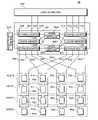
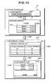
- FIG. 1is a diagram showing the hardware structure of a storage system according to an embodiment of this invention.
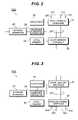
- FIG. 2is a diagram showing the hardware structure of a channel adapter.
- FIG. 3is a diagram showing the hardware structure of a storage adapter.
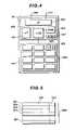
- FIG. 4is a diagram showing the hardware structure of a flash memory module.
- FIG. 5is an explanatory diagram showing the block in a flash memory module.
- FIG. 6is an explanatory diagram showing the outline of processing performed by a storage controller to write data in a flash memory module.
- FIG. 7is an explanatory diagram showing the outline of processing performed by the storage controller to detect an address error when it occurs in a flash memory module.
- FIG. 8is a diagram showing the hardware structure of a storage channel interface.
- FIG. 9is an explanatory diagram showing the information stored in a PDEV management table.
- FIG. 10is an explanatory diagram showing the information stored in a media database.
- FIG. 11is a flowchart showing a data read processing routine performed by the storage controller.
- FIG. 12is an explanatory diagram showing a method for converting a cache address to a logical address.
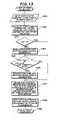
- FIG. 13is a flowchart showing a data write processing routine performed by the storage controller.
- FIG. 14is a flowchart showing error correction processing performed by the storage channel interface.
- FIG. 15is a diagram explaining the operations performed, when data writing, by the storage controller to add a different type of protection code to data to protect it from address errors.
- FIG. 16is a diagram explaining the operations performed, when an address error occurs in a flash memory module, by the storage controller to detect the address error based on a protection code including write-time information.
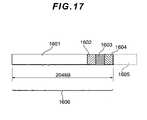
- FIG. 17is a diagram explaining an example of other different types of protection codes added to a page data section when writing data.
- FIG. 1shows the hardware structure of a storage system 10 according to this embodiment.
- This storage system 10has a storage controller SC and flash memory modules P 00 to P 33 .
- the storage controller SChas channel adapters CA 0 and CA 1 ; cache memory CM 0 and CM 1 ; storage adapters SA 0 and SA 1 ; and interconnection networks NW 0 and NW 1 .
- FIG. 1shows an example where the storage controller SC has two channel adapters CA 0 and CA 1 , two cache memory CM 0 and CM 1 , and two storage adapters SA 0 and SA 1 , however, there may be any number of components.
- the interconnection networks NW 0 and NW 1are, for example, switches that connect the respective components in the storage controller SC to one another. More specifically, they connect the channel adapter CA 0 , cache memory CM 0 and storage adapter SA 0 to one another. Likewise, they also connect the channel adapter CA 1 , cache memory CM 1 and storage adapter SA 1 to one another.
- the channel adapter CA 0is connected to a host computer 100 via channels C 00 , C 01 , C 02 and C 03 .
- the channel adapter CA 1is connected to the host computer 100 via channels C 10 , C 11 , C 12 and C 13 .
- the host computer 100is, for example, a personal computer, work station, or mainframe computer and requests data reading from and writing to the storage system 10 .
- the cache memory CM 0 and CM 1temporarily store data they receive from the channel adapters CA 0 and CA 1 or storage adapters SA 0 and SA 1 .
- the storage adapter SA 0is connected to the flash memory modules P 00 to P 33 . More specifically, the storage adapter SA 0 is connected to the flash memory modules P 00 to P 03 via a channel D 00 . It is also connected to the flash memory modules P 10 to P 13 via a channel D 01 . It is also connected to the flash memory modules P 20 to P 23 via a channel D 02 , and connected to flash memory modules P 30 to P 33 via a channel D 03 .
- the storage adapter SA 1is connected to the flash memory modules P 00 to P 33 . More specifically, it is connected to flash memory modules P 00 to P 03 via a channel D 10 . It is also connected to the flash memory modules P 10 to P 13 via a channel D 11 . It is also connected to the flash memory modules P 20 to P 23 via a channel D 12 , and connected to the flash memory modules P 30 to P 33 via a channel D 13 .
- the channel adapters CA 0 and CA 1 and storage adapters SA 0 and SA 1are connected to a maintenance terminal SVP.
- This maintenance terminal SVPsends configuration information input from the administrator of the storage system 10 to the channel adapters CA 0 and CA 1 and/or storage adapters SA 0 and SA 1 .
- the storage system 10may have only one adapter instead of having the storage adapters SA 0 and channel adapter CA 0 . In that case, that one adapter carries out the processing the storage adapter SA 0 and channel adapter CA 0 usually perform.
- VDEV 0 to VDEV 3are RAID (Redundant Arrays of Inexpensive Disks) groups.
- the RAID group VDEV 0is composed of the flash memory modules P 00 , P 10 , P 20 and P 30 .
- the datacan be rebuilt using the other flash memory modules P 10 , P 20 and P 30 in the RAID group VDEV 0 .
- FIG. 2shows the hardware structure of the channel adapter CA 0 .
- the channel adapter CA 0has a host channel interface 21 , cache memory interface 22 , network interface 23 , processor 24 , local memory 25 and processor peripheral control unit 26 .
- the host channel interface 21is an interface that connects the channel adapter CA 0 to the host computer 100 via the channels C 00 , C 01 , C 02 and C 03 . It converts data transfer protocols in the channels C 00 , C 01 , C 02 and C 03 to data transfer protocols for the storage controller SC, or vice versa.
- the cache memory interface 22is an interface that connects the channel adapter CA 0 to the interconnection networks NW 0 and NW 1 .
- the network interface 23is an interface that connects the channel adapter CA 0 to the maintenance terminal SVP.
- the host channel interface 21 and cache memory interface 22are connected to each other via a signal line 27 .
- the processor 24carries out various kinds of processing by executing the programs stored in the local memory 25 . More specifically, the processor 24 controls data transfer between the host computer 100 and interconnection networks NW 0 and NW 1 .
- the local memory 25stores the programs the processor 24 executes. It also stores the tables the processor 24 refers to.
- the tables referred to by the processor 24are set or changed by the administrator. More specifically, the administrator inputs information regarding table setup or change(s) in table(s) in the maintenance terminal SVP.
- the maintenance terminal SVPsends the input information to the processor 24 via the network interface 23 .
- the processor 24then creates a table or makes change(s) in the table(s) based on the information it receives. Then, the processor 24 stores the table in the local memory 25 .
- the processor peripheral control unit 26controls data transfer between the host channel interface 21 , cache memory interface 22 , network interface 23 , processor 24 and local memory 25 .
- An example of the processor peripheral control unit 26is a chipset.
- the hardware structure of the channel adapter CA 1is the same as that of the channel adapter CA 0 , so explanations for the hardware structure of the channel adapter CA 1 will be omitted.
- FIG. 3shows the hardware structure of the storage adapter SA 0 .
- the storage adapter SA 0has a cache memory interface 31 , storage channel interface 32 , network interface 33 , processor 34 , local memory 35 and processor peripheral control unit 36 .
- the cache memory interface 31is an interface that connects the storage adapter SA 0 to the interconnection networks NW 0 and NW 1 .
- the storage channel interface 32is an interface that connects the storage adapter SA 0 to the channels D 00 , D 01 , D 02 and D 03 . It converts data transfer protocols in the channels D 00 , D 01 , D 02 and D 03 to data transfer protocols for the storage controller SC, or vice versa.
- the cache memory interface 31 and storage channel interface 32are connected to each other via a signal line 37 .
- the network interface 33is an interface that connects the storage adapter SA 0 to the maintenance terminal SVP.
- the processor 34carries out various kinds of processing by executing the programs stored in the local memory 35 .
- the local memory 35stores the programs the processor 34 executes. It also stores the tables the processor 34 refers to.
- the tables referred to by the processor 34are configured or changed by the administrator. More specifically, the administrator inputs information regarding table setup or change(s) in table(s) into the maintenance terminal SVP.
- the maintenance terminal SVPsends the input information to the processor 34 via the network interface 33 .
- the processor 34then creates a table or makes change(s) in the table(s) based on the information it receives. Then, the processor 34 stores the table in the local memory 35 .
- the processor peripheral control unit 36controls data transfer between the cache memory interface 31 , storage channel interface 32 , network interface 33 , processor 34 , and local memory 35 .
- An example of the processor peripheral control unit 36is a chipset.
- the hardware structure of the storage adapter SA 1is the same as that of the storage adapter SA 0 , so explanations for the hardware structure of the storage adapter SA 1 will be omitted.
- FIG. 4shows the hardware structure of the flash memory module P 00 .
- the flash memory module P 00has a memory controller MC and flash memory MEM.
- the flash memory MEMstores data.
- the memory controller MCcontrols data reading, writing, and erasing from/to the flash memory MEM.
- the memory controller MChas a processor ( ⁇ P) 401 , interface unit (I/F) 402 , data transfer unit (HUB) 403 , memory (RAM) 404 , and memory (ROM) 407 .
- the flash memory MEMhas a plurality of flash memory chips 405 .
- Each flash memory chip 405includes a plurality of blocks 406 each storing data.
- the blocks 406are units the memory controller MC erases data in.
- Each block 406includes a plurality of pages. Pages are units the memory controller MC reads/writes data in.
- the pagesare classified into valid pages, invalid pages, unused pages, and bad pages.
- Valid pagesstore valid data.
- Invalid pagesstore invalid data.
- Unused pagesstore no data.
- Bad pagescannot be used physically for reasons such as the storage elements in those bad pages being broken.
- the interface unit 402is connected to the storage adapter SA 0 in the storage controller SC via the channel D 00 . It is also connected to the storage adapter SA 1 in the storage controller SC via the channel D 10 . It receives commands from the storage adapters SA 0 and SA 1 .
- the commands from the storage adapters SA 0 and SA 1are, for example, SCSI commands.
- the interface unit 402receives data from the storage adapters SA 0 and SA 1 . Then, it stores that data in the memory 404 . It also sends the data stored in the memory 404 to the storage adapters SA 0 and SA 1 .
- the interface unit 402serves as an interface compatible with hard disk drives. Accordingly, the storage adapters SA 0 and SA 1 recognize the flash memory modules P 00 to P 33 as, for example, hard disk drives where one sector has 512 bytes.
- the storage system 10can have both flash memory modules and hard disk drives as data-storing media.
- the memory 404is, for example, dynamic random access memory that enables high-speed reading/writing. It temporarily stores data the interface unit 402 sends/receives. Meanwhile, the memory 407 is a nonvolatile memory and stores programs the processor 401 executes. The programs executed by the processor 401 are loaded from the memory 407 into the memory 404 at the startup of the storage system 10 so that the processor 401 can execute the programs. The memory 404 also stores a table the processor 401 refers to.
- the table referred to by the processor 401is, for example, an address translation table for translating a logical address in flash memory MEM to a physical address or vice versa.
- a logical addressis used when access is made from outside the flash memory module P 00 (e.g., the storage adapter SA 0 ) to a page, which is a unit of data reading/writing from/to the flash memory MEM.
- a physical addressis used when the memory controller MC accesses a page.
- the data transfer unit 403is, for example, a switch, and connects the processor 401 , interface unit 402 , memory 404 , memory 407 , and flash memory MEM to one another and controls data transfer between them.
- the processor 401carries out various kinds of processing by executing the programs stored in the memory 404 . For example, it refers to the address translation table in the memory 404 , translates a logical address in the flash memory MEM to a physical address or vice versa, and reads/writes data from/to the flash memory MEM.
- the processor 401also carries out reclamation (or ‘garbage collection’) (block reclamation process) and wear-leveling for the blocks 406 in the flash memory module P 00 .
- Reclamationis the reproduction of an invalid page in a block 406 to an unused page so that the block where the number of unused pages is small can be used again. More specifically, it is assumed that a reclamation target block (target block) 406 includes valid pages, invalid pages, and unused pages, and that the number of invalid pages is large. In order to increase the number of unused pages, the invalid pages have to be erased. However, data can only be erased in block units, not in page units. Therefore, the valid pages are copied to another block having empty space and the target block is erased and reproduced.
- the processor 401copies the data stored in the valid pages in the reclamation target block (target block) 406 to an unused block. Then, it changes the logical block number of the unused block having the copied data to the logical block number of the target block. Then, it erases all the data in the target block and the reclamation is complete.
- the processor 401writes data in the block 406 , the number of unused pages in the block 406 decreases.
- the processor 401can no longer write data in the block 406 . Therefore, it carries out reclamation for the target block 406 to change the invalid pages to unused pages.
- wear-levelingis the leveling of the number of data erase cycles of the blocks 406 . Wear-leveling makes it possible to lengthen the duration of the flash memory MEM. This is because the flash memory MEM wears out when the number of data erase cycles reaches a large number. Normally, the flash memory MEM is guaranteed ten thousand to one hundred thousand erase cycles.
- FIG. 5is an explanatory diagram showing a block 406 in the flash memory module P 00 .
- the block 406includes a plurality of pages 501 —numbering in the tens of pages—(e.g., 64 pages).
- the memory controller MCreads/writes data in page units. For example, in NAND flash memory, the memory controller MC reads data at a speed of 20 ⁇ s to 30 ⁇ s/page and writes data at a speed of 0.2 ms to 0.3 ms/page. Also, it erases data at a speed of 2 mn to 4 ms/block.
- Each page 501includes a data section 502 and redundant section 503 .
- the data section 502is 2048 bytes and the redundant section 503 is 64 bytes.
- This embodimentis explained giving an example of a flash memory where each page 501 is composed of 2112 bytes and the data section 502 in that page 501 is of 2048 bytes; however, the page size is not limited.
- the data section 502stores user data.
- the redundant section 503stores the mapping and management information and an error correction code for the relevant page 501 .
- the mapping and management informationincludes an offset address and page status.
- the offset addressis a relative address in the block 406 the page 501 belongs to.
- the page statusindicates whether the page 501 is a valid page, invalid page, unused page or in-process page.
- An error correction codeis for detecting and correcting an error in the page 501 and is, for example, a Hamming code.
- only the memory controller MCcan access the redundant section 503 and the storage adapters SA 0 and SA 1 can access only the page data section 502 .
- logical addressesare for mapping memory spaces in the data section 502 .
- the data written in an area in the flash memory modulesometimes migrates to another area within that flash memory module, independently of instructions from the storage controller SC.
- the memory controller MCreflects the data migration result in the address translation table correctly, so that the storage controller SC can access the correct data.
- FIG. 6shows the outline of the processing the storage controller SC performs to write data in the flash memory module P 00 .
- data 601is managed in units of sectors in hard disk drives requiring high reliability(e.g., in 520-byte units).
- Each 520-byte piece of data 601is composed of 512-byte user data and an 8-byte hard disk drive protection code.
- the hard disk drive protection codeincludes the information that enables identification of address information (write address) for a data write destination hard disk drive.
- the storage system 10can have both flash memory modules and hard disk drives as data-storing media, and in the cache memory CM, data is managed in units of sectors in hard disk drives.
- an address for accessing data 601 in the cache memory CMis called a cache address.
- the storage controller SCTo write data in the flash memory module P 00 , the storage controller SC first transfers the data 601 in the cache memory CM to the storage adapter SA (Step 602 ).
- the storage adapter SAchecks the size of the page data section used in the write destination flash memory module P 00 and calculates the start logical address of the write destination (details will be given later).
- the logical address of the write destinationis ‘A0.’
- the storage adapter SAcreates a protection code 604 which enables identification of the write destination logical address information.
- This protection code 604is not necessarily a logical address and it only has to be information enabling identification of the write destination logical address.
- the protection code 604includes, for example, a part or all of the logical address, or information where the logical address is encoded.
- the storage adapter SAthen attaches the protection code 604 to the write data 603 to protect it from address errors.
- the storage adapter SAdivides the data 601 into pieces so that the size of each piece of divided write data 603 in combination with its protection code 604 matches the size of each page data section in the write destination flash memory module P 00 .
- the storage adapter SAadjusts the boundaries of the write data 603 so that the data 601 , which is managed in 520-byte units in the cache memory CM, and its protection code 604 together will be 2048 bytes.
- the storage adapter SAthen transfers the write data 603 and protection code 604 , which have been adjusted in size to match the page data section size in the flash memory module P 00 , to the flash memory module P 00 (Step 605 ).
- the memory controller MCHaving received the write data 603 , the memory controller MC refers to the address translation table 606 and obtains the write destination physical address. According to the address translation table 606 in this example, the logical address ‘A0’ is associated with the physical address ‘b0’ and the logical address ‘A1’ is associated with the physical address ‘b1.’
- the memory controller MCwrites the write data 603 and protection code 604 it receives from the storage adapter SA in the page data section having the physical address ‘b0’ (Step 607 ).
- the memory controller MChandles the protection code 604 as data and writes it in the flash memory MEM.
- the memory controller MCcarries out write operations based on write destination logical address information it received in addition to a Write command. Likewise, it carries out read operations based on read source logical address information it received in addition to a read command.
- the logical address information the memory controller MC receives in addition to a commandis a sector address in the case where one sector capacity is 512 bytes same as a hard disk drive which do not require high reliability.
- the memory controller MCaccesses the flash memory, it translates the received sector address to a logical address, and further to a physical address.
- the sector addresses corresponding to a start page-data sectionlogical address ⁇ 4.
- reference numeral 608shows the page having physical address ‘b0’ and reference numeral 609 shows the page having physical address ‘b1.’
- the reference numeral 610shows redundant sections used by the memory controller MC.
- FIG. 7shows the outline of the processing the storage controller SC performs to detect an address error when it occurs inside the flash memory module P 00 .
- the logical address ‘A0’must be associated with the physical address ‘b0’ but this physical address ‘b0’ is mistakenly replaced with ‘b1’ in the address translation table 606 (Step 710 ) is explained.
- the storage controller SCtries to read the data in the page data section corresponding to the logical address ‘A0’ but because there is an address error in the address translation table 606 , the memory controller MC reads the data in the page data section having the physical address ‘b1’ (Step 707 ) and transfers it to the storage adapter SA (Step 705 ).
- the storage adapter SAchecks the protection code 704 attached to the data 703 read from the flash memory module P 00 . More precisely, the storage adapter SA compares the logical address information ‘A1’ identified with the protection code 704 attached to the read data 703 with the logical address ‘A0,’ which is where the storage adapter SA requested the memory controller MC to read data from; and checks whether the data 703 is being read correctly. Because the address translation table 606 has an address error, the logical address information ‘A1’ identified with the protection code 704 does not match the logical address ‘A0,’ which is where the storage adapter SA requested the memory controller MC to read data from. That is how the storage adapter SA can detect the address error. When the storage adapter SA detects an address error, it does not store read data 703 in the cache memory CM (Step 702 ) because it is not the data that was intended to be read.
- FIG. 8shows the hardware structure of the storage channel interface 32 .
- This storage channel interface 32has a function that attaches a protection code to write data and detects an address error in read data. It has a media identification unit 801 , XOR engine 804 , switch (SW 1 ) 805 , switch (SW 2 ) 806 , protection code check unit (LA check unit) 808 , protection code attaching unit (LA attaching unit) 809 , and data aligner 810 .
- the storage channel interface 32is connected to the processor peripheral control unit 36 (see FIG. 3 ) via the channel 812 .
- the media identification unit 801has the information for identifying the types of storage media connected to the storage system 10 and the information for calculating write destination logical addresses. More precisely, the media identification unit 801 has a media database 803 and PDEV management table 802 . Details of the media database 803 and PDEV management table 802 will be given later.
- the XOR engine 804creates parity data to be stored in RAID groups. It also rebuilds data that has been lost during the occurrence of an error.
- the XOR engine 804is connected to both the switch 805 and signal line 37 .
- the switches 805 and 806switch data input/output paths based on the result of identification by the media identification unit 801 . For example, if a data write destination or data read source is a hard disk drive, the switches 805 and 806 are operated so that the channel 811 is set as a data input/output path. Meanwhile, if a data write destination or data read source is a flash memory module, the switches 805 and 806 are operated so that the channel 807 is set as a data input/output path.
- a data read sourceis a flash memory module
- the read datapasses through the protection code check unit 808 and data aligner 810 .
- a data write destinationis a flash memory module
- the write datapasses through the data aligner 810 and protection code attaching unit 809 .
- the switch 806is connected to the channels D 00 to D 03 .
- the data aligner 810adjusts the boundaries of data, which is managed in 520-byte units in the cache memory CM, so that the size of the data including the protection code matches the size of the page data section.
- the data aligner 810removes the protection code from read data and adjusts the boundaries of the read data minus the protection code so that the size of the read data matches the management unit in the cache memory CM (i.e., 520 bytes).
- the protection code attaching unit 809Based on the information (the page data section size etc.) obtained from the media identification unit 801 , the protection code attaching unit 809 creates a protection code enabling identification of the logical page address information for the write destination page in the flash memory module and attaches that protection code to the write data.
- the protection code check unit 808checks whether the logical address identified with the protection code attached to the read data matches the logical address of the data that is intended to be read.
- FIG. 9shows the information stored in the PDEV management table 802 .
- This PDEV management table 802manages the information regarding the storage media (PDEVs) connected to the storage system 10 .
- the storage channel interface 32sends inquiry commands to the respective storage media connected to the storage system 10 and, based on the responses to the inquiry commands, stores the module names 901 , vendor names 902 , and types 903 of the storage media in the PDEV management table 802 .
- the storage channel interface 32also searches the media databases 803 for media types 904 and page data section sizes 905 corresponding to the vendor names and types included in the responses to the inquiry commands and stores them in the PDEV management table 802 .
- the storage channel interface 32can be aware of the types and page data section sizes (or sector capacities) of the storage media connected to the storage system 10 .
- FIG. 10shows the information stored in the media database 803 .
- This media database 803stores vendor names 902 , types 903 , media types 904 , and page data section sizes 905 of the storage media (e.g., flash memory modules and hard disk drives) that may be possibly connected to the storage system 10 .
- the media type 904is information for identifying whether storage media is a flash memory module or hard disk drive. If the storage media is a flash memory module, ‘1’ is entered in the media type 904 box. Meanwhile, if the storage media is a hard disk drive, ‘0’ is entered in the media type 904 box. When the storage medium is a hard disk drive, the capacity of one sector is entered in the page data section size 905 box.
- the administratorcan modify the existing data in the media database 803 or add more information using the maintenance terminal SVP (see FIG. 1 ).
- the maintenance terminal SVPsee FIG. 1
- a protection codeenabling identification of a write destination logical address can be attached to the data.
- FIG. 11is a flowchart showing a data read processing routine performed by the storage controller SC.
- the storage controller SCinputs a read source cache address LA and read data length DL in the storage channel interface 32 (Step 1101 ).
- the storage channel interface 32then resets the retry counter (Step 1102 ).
- the storage channel interface 32calculates the range of logical addresses in the read source flash memory module (start logical address PA 1 , offset value OS 1 , end logical address PA 2 , and offset value OS 2 ) (Step 1103 ). The method for calculating these addresses and values will be described later.
- the storage channel interface 32then reads the data (i.e., the data stored in the areas ranging from the start logical address PA 1 to the end logical address PA 2 ) from the flash memory module (Step 1104 ).
- the storage channel interface 32compares the logical address identified with the protection code attached to the read data with the logical address of the data that is intended to be read; and checks whether an address error has occurred or not (Step 1105 ). Here, if no address error is found (Step 1105 ; Yes), the processing proceeds to Step 1106 , but if an address error is found (Step 1105 ; No), it proceeds to Step 1107 .
- the storage channel interface 32removes the protection code from the read data and adjusts the boundaries of the data so that the data size matches the management unit in the cache memory CM (Step 1106 ). The storage channel interface 32 then stores the data in the cache memory CM and completes the read operation.
- Step 1107the storage channel interface 32 increments the retry counter by one (Step 1107 ) and, if the retry counter value has not reached a specified number (Step 1108 ; No), it repeats the data read operation (Step 1104 ).
- Step 1108the storage channel interface 32 executes error correction processing (Step 1109 ).
- FIG. 12shows a method for translating a cache address to a logical address.
- a start logical address PA 1 , offset value OS 1 , end logical address PA 2 and offset value OS 2are calculated using the formulas (1) to (4) below.
- PA 1int ⁇ ( LA 1* X )/( PS ⁇ Y ) ⁇ (1)
- PA 2int[ ⁇ ( LA 1+ DL )* X ⁇ 1 ⁇ /( PS ⁇ Y )] (2)
- OS 1LA 1* X ⁇ PA 1*( PS ⁇ Y ) (3)
- OS 2( LA 1+ DL )* X ⁇ 1 ⁇ PA 2*( PS ⁇ Y ) (4)
- Xis a unit for data management in the cache memory
- LA 1is the start cache address of the read/write range
- LA 2is the end cache address of the read/write range
- DLis the size of read/write data
- PSis the size of a page data section in a flash memory module
- Yis the size of a protection code.
- the example shown in FIG. 12is for where data is located at the start address side in the page data section and a protection code is located at the end address side in the page data section; however, the locations of the data and protection code are not limited to these places.
- PA 1is the logical address of the start page data section 1101 in a flash memory module from/to which data is written/read.
- PA 2is the logical address of the end page data section 1102 in the flash memory module from/to which the data is to be written/read.
- the size of the access target data ranging from PA 1 to PA 2 in the flash memory moduleis larger than the size of the target read/write data DL in the cache memory.
- the surplus parts of the data in the flash memory moduleare called offsets.
- the start page data section 1101has an offset 1103 .
- the end page data section 1102has an offset 1104 .
- OS 1 and OS 2are addresses in the page data sections.
- the space from the address LA 1 to address LA 2 in the cache memorycorresponds to the space from the address OS 1 in the start page data section 1101 (i.e., the page data section identified by the logical address PA 1 ) to the address OS 2 in the end page data section 1102 (i.e., the page data section identified by the logical address PA 2 ) in the flash memory module.
- the storage controller SCreads the data in the whole page data sections including the offsets 1103 and 1104 in the flash memory module; removes the offsets 1103 and 1104 from the data; and stores the read data in the cache memory.
- the media database 803stores, for the respective storage media having different specifications, address translation formulas such as the formulas (1) to (4) for translating logical addresses to physical address or vice versa, it is easy to handle storage media with different address translation styles.
- FIG. 13is a flowchart showing a data write processing routine performed by the storage controller SC.
- the storage controller SCinputs, in the storage channel interface 32 , the start cache address LA of a write destination and the size DL of the write data (Step 1301 ).
- the storage controller SCcalculates the range of logical addresses for the write destination in a flash memory module (start logical address PA 1 , offset value OS 1 , end logical address PA 2 , and offset value OS 2 ) (Step 1302 ).
- Step 1303If the start page data section 1101 has an offset 1103 (Step 1303 ; No), the storage controller SC reads the data in the start page data section 1101 (Step 1304 ). Meanwhile, if the start page data section 1101 does not have an offset 1103 (Step 1303 ; Yes), the storage controller SC proceeds to Step 1305 .
- Step 1305If the end page data section 1102 has an offset 1104 and the data in the end page data section has not been read yet (Step 1305 ; Yes), the storage controller SC reads the end page data section 1102 (Step 1306 ). Meanwhile, if the end page data section 1102 does not have an offset 1104 or the data in the end page data section has already been read (Step 1305 ; No), the storage controller SC proceeds to step S 1307 .
- the storage controller SCWhen the storage controller SC has read the start page data section 1101 or end page data section 1102 , it does not update the data in the offsets 1103 and 1104 but updates the data except for the offsets 1103 and 1104 to the write data in the cache memory CM. The storage controller SC then attaches a protection code enabling identification of the write destination logical address to the data in cache memory and adjusts the boundaries of that data so that the data size including the protection code matches the page data section size (Step 1307 ).
- the storage controller SCthen transfers the write data from the start logical address PA 1 to the end logical address PA 2 to the flash memory module (Step 1308 ) and completes the write processing.
- FIG. 14is a flowchart showing error correction processing performed by the storage channel interface 32 .
- the case where an address error occurs in the logical address PA 1 in the flash memory module P 00 belonging to the RAID group VDEV 0 consisting of the flash memory modules P 00 , P 10 , P 20 and P 30is discussed.
- the storage channel interface 32reads data from the logical address PA 1 in the flash memory modules P 10 , P 20 and P 30 belonging to the same RAID group VDEV 00 as the flash memory module P 00 (Step 1401 a , 1401 b , and 1401 c ).
- the storage channel interface 32removes the flash memory protection code enabling identification of the logical address from the data that has been read (Step 1402 a , 1402 b , and 1402 c ).
- the storage channel interface 32then divides the data that has been read into pieces so that the size of each piece of divided data matches the management unit in the cache memory (Step 1403 a , 1403 b , and 1403 c ).
- the storage channel interface 32then removes a hard disk drive protection code from each piece of data whose size matches the management units in the cache memory (Steps 1404 a , 1404 b , and 1404 c ).
- the XOR engine 804calculates exclusive OR for the data minus the flash memory protection code and hard disk drive protection code, and rebuilds the data that must have been stored in the flash memory module P 00 (Step 1405 ).
- the storage channel interface 32attaches a hard disk drive protection code to the rebuilt data (Step 1406 ).
- the storage channel interface 32also attaches a flash memory module protection code (information enabling identification of the write destination logical address PA 1 ) to the rebuilt data; and adjusts the boundaries of the data so that the size of each piece of data matches the page data section size (Step 1407 ).
- a flash memory module protection codeinformation enabling identification of the write destination logical address PA 1
- the storage channel interface 32then writes the rebuilt data in the logical address PA 1 in the flash memory module P 00 (Step 1408 ), completing the error correction process.
- the storage controller SCwhen an address error occurs in a hard disk drive, the storage controller SC overwrites/corrects the data having the address error in units of a first data length.
- FIG. 15is a diagram explaining operations the storage controller SC performs during data writing to attach a different type of protection code to data protect it from address errors. For example, when the storage controller SC writes sequential access data in the flash memory module P 00 , it attaches, to the sequential access data, protection codes including write-time information.
- data 1401is managed in units of sectors in hard disk drive sectors (e.g., in 520-byte units).
- the storage controller SCwrites data in the flash memory module P 00 , it transfers the data 1401 in the cache memory CM to the storage adapter SA (Step 1402 ).
- the storage adapter SAwrites sequential data 1403 in the logical addresses A 0 to A 2 in the write destination flash memory module P 00 is discussed below.
- the storage adapter SAcreates protection codes 1404 enabling identification of the write destination logical addresses A 0 to A 2 and the write-time information ‘t1.’
- the storage adapter SAthen transfers the pieces of the write data 1403 and their protection codes 1404 , the size of each set being adjusted to match the page data section size, to the flash memory module P 00 (Step 1405 ).
- the memory controller MCHaving received the write data, the memory controller MC refers to the address translation table 1406 and translates the physical addresses of the write destination. According to the address translation table 1406 , logical addresses A 0 to A 2 correspond to physical addresses b 0 to b 2 , respectively.
- the memory controller MCstores the pieces of write data together with their protection codes enabling identification of the logical addresses A 0 to A 2 and write-time information t 1 , in the page data sections 1408 having the physical addresses b 0 to b 2 , respectively.
- the reference numeral 1410shows the redundant sections used by the memory controller MC.
- FIG. 16is a diagram explaining operations the storage controller SC performs to detect an address error based on protection codes including write-time information when an address error occurs in a flash memory module.
- the reference numeral 1508shows the page having the physical address b 1 and the reference numeral 1509 shows the page having physical address b 4 .
- the reference numeral 1410shows the redundant sections used by the memory controller MC.
- the storage controller SCtries to read the sequential data in the logical addresses A 0 to A 2 . However, even if the storage controller SC tries to read the data stored in the page data section in the logical address A 1 , due to the address error in the address translation table 1406 , the memory controller MC reads data in the page data section in the wrong physical address b 4 (Step 1507 ) and transfers that data to the storage adapter SA (Step 1505 ).
- the storage adapter SAthen checks the protection code 1504 attached to the received data 1503 . However, because the protection code contained in the data read from the physical address b 4 identifies the logical address A 1 , the storage adapter cannot detect an address error just by checking the logical address.
- the storage adapter SAcan detect an address error.
- Step 1502Data found to have been involved in an address error is not to be stored in the cache memory CM.
- each protection codeinclude, in addition to information enabling identification of a logical address, information enabling identification of a write-time.
- a protection codemay alternatively include, in place of write-time information, an identifier of an exchange write data belongs to or sequence identifier, or information where write-time information is encoded. It is also possible to have the storage adapter SA include a table storing relationships between the logical address information for the respective pieces of write data and the write-time information for the same so that, when reading data, the storage adapter SA can compare the write-time information identified based on the relevant data's protection codes and the corresponding records in the table.
- FIG. 17is a diagram explaining an example of other types of protection codes attached to a page data section during writing.
- a pageincludes a page data section 1606 and redundant section 1605 . Because the storage controller SC cannot read/write data in the redundant sections 1605 , protection codes are written in a predetermined area in the page data section 1606 , together with the data 1601 . The data 1601 and the protection codes 1602 , 1603 and 1604 are written in the page data section 1606 .
- the protection code 1602includes information enabling identification of a logical address.
- the protection code 1603includes information enabling identification of a write-time.
- the protection code 1604is for detecting or correcting an error in the data 1601 , protection code 1602 or 1603 written in the page data section 1606 .
- Examples of the protection code 1604include a CRC (Cyclic Redundancy Check) code, a LRC (Longitudinal Redundancy Check) code and a Hamming code.
- the memory controller MCstores a protection code for the data written in a page data section in a redundant section 1605 and the data is guaranteed by this protection code.
- the protection code in the redundant section 1605is removed during data transfer between the memory controller MC and storage adapter SA, so a consistent data guarantee cannot be provided in both the storage adapter SA and flash memory modules.
- an error correction code in a page data sectionthe reliability of the storage system can be improved.
Landscapes
- Engineering & Computer Science (AREA)
- Theoretical Computer Science (AREA)
- Physics & Mathematics (AREA)
- General Engineering & Computer Science (AREA)
- General Physics & Mathematics (AREA)
- Quality & Reliability (AREA)
- Computer Security & Cryptography (AREA)
- Memory System Of A Hierarchy Structure (AREA)
- Techniques For Improving Reliability Of Storages (AREA)
- Read Only Memory (AREA)
Abstract
Description
- This application relates to and claims priority from Japanese Patent Application No. 2006-178487, filed on Jun. 28, 2006, the entire disclosure of which is incorporated herein by reference.
- The invention relates to a storage system using flash memory as storage media, and to a data protection method for that storage system.
- Storage systems usually have randomly accessible nonvolatile storage media. Examples of the randomly accessible nonvolatile storage media include magnetic disks and optical disks. Recent mainstream storage systems include many small disk drives. Also, as semiconductor technology progresses, block-erasable nonvolatile semiconductor memory has been developed. Block-erasable nonvolatile semiconductor memory is, for example, flash memory. Storage systems using flash memory as storage media are superior to storage systems having many small disk drives in service life, power-saving, and access time.
- Flash memory is explained below. In flash memory, data is erased in units of blocks and read/written in units of pages, blocks and pages both being memory areas. It is a characteristic of flash memory that data cannot be directly updated. More specifically, when updating data in flash memory, valid data stored in the flash memory is copied in another place at first. Then, the data is erased in block units. Then, new data is written in the freshly-erased block where the old data had been stored.
- More specifically, with flash memory, it is possible to set bit ‘1’ to ‘0’ but not ‘0’ to ‘1.’ Therefore, to update data in flash memory, block(s) are erased. As explained above, data update in flash memory requires erasing of blocks.
- However, the time required for erasing one block in flash memory is longer than the time required for writing data in one page, by an order of magnitude. Accordingly, if one block is erased every time data in one page is updated, the data update capacity of flash memory deteriorates to a considerable extent. In other words, with flash memory, it is necessary to write data with an algorithm that enables concealment of erase times.
- Also, flash memory has a finite number of block-erase cycles. For example, one hundred thousand erase cycles are guaranteed per one block.
- Accordingly, there is a problem with blocks with a large number of erase cycles due to a concentration of data update, in that the data can no longer be erased and the blocks cannot be used anymore. Accordingly, storage systems using flash memory as storage media need wear-leveling processes so that erasing will not be concentrated on a certain block.
- When writing data in a flash memory module, address translation is performed for erase-time concealment and wear-leveling. A flash memory module has one or more flash memory chips and a memory controller for controlling data transfer to the flash memory chip(s). In order to avoid concentration of data writing on a particular physical address, the memory controller has the function of converting a logical address—a write destination address—it receives from a host computer or the controller of a storage apparatus to a physical address, which is a write destination address in the flash memory chip. Here, the problem is an address error that may occur in the memory controller. If the memory controller causes an error when converting a logical address to a physical address, data is written in the wrong physical address. In other words, the write data itself has no problems or errors, but because it is written in the wrong physical address, there is a possibility that the data may not be read when desired.
- The technique disclosed in Japanese Patent Laid-Open Publication No. 2001-202295 has been known as a method for solving the foregoing problem. With this technique, when using hard disk drives as storage media, data is protected from address errors in the storage media. More specifically, when writing data in a hard disk drive, the data is given protection codes including logical address values, the protection codes corresponding to the respective logical data blocks in the hard disk drive. When reading data from the hard disk drive, the protection codes given to the respective logical data blocks are checked.
- Moreover, US Patent Publication No. 2004-0148461A1 discloses a storage system that guarantees compatibility between storage media having different data management units.
- In flash memory, data is read/written using addresses mapped onto each page. The page size differs depending on the chip type and generation. For example, the page size of a current flash memory chip is 528 bytes or 2112 bytes and the size of the memory area data actually can be written in from outside a flash memory module is 512 bytes or 2048 bytes in the page. The rest of the page (e.g., 528 bytes minus 512 bytes, equal to 16 bytes; and 2112 bytes minus 2048 bytes, equal to 64 bytes) is used as a redundant section for storing information for a memory controller to manage addresses in page units and error correction codes for the memory controller to correct errors. With the trend in increasing flash memory capacity, the page size is expected to increase in size.
- Flash memory modules intended to substitute for hard disk drives as storage media in storage systems have hard disk drive-compatible interfaces.
- Storage controllers recognize hard disk drive-compatible flash memory modules as hard disk drives each having 512 bytes per sector. In other words, the storage controllers cannot recognize the address-converted data units in the flash memory modules with the hard disk drive-compatible interfaces. Moreover, the page size differs depending on the type and generation of the flash memory chips implemented in the flash memory modules. In the foregoing conventional measures against address errors, it is necessary for storage controllers to add, to each data unit whose address is to be converted, a protection code to perform data writing.
- However, as already mentioned above, with the flash memory modules having hard disk drive-compatible interfaces or flash memory modules having unclear chip specifications, the size of data to be protected from address errors is unclear. For this reason, it is difficult to protect data from address errors in the flash memory modules using conventional techniques.
- In a hard disk drive requiring high reliability, the capacity of one sector is 520 bytes and data and protection codes are managed as a set. Meanwhile, in flash memory, the sizes of data that can be written in one page are multiples of 512 bytes, except for the memory areas used for management by the memory controller. If the data managed in 520-byte units is directly written in page(s) in the flash memory, the 520-byte pieces of data are written in the flash memory, sometimes spreading across the page boundaries. This means that the data and its protection code in one 520-byte piece are written in different pages and the data separated from the protection code is no longer protected from address errors. Accordingly, it is difficult to protect data spreading across the page boundaries from address errors using conventional techniques.
- This invention was devised in light of the foregoing problems, and aims to provide a storage system able to correct address errors in flash memory modules that use different data management units from those used in hard disk drives; and a data protection method for this storage system.
- In order to solve the foregoing problems, this invention provides a storage system including: one or more flash memory modules each having one or more flash memory chips and a memory controller that controls reading/writing of data from/to the flash memory chips; and a storage controller having cache memory that temporarily stores data read/written from/to one or more of the flash memory chips. In the cache memory, data read/written from/to the flash memory chips is managed in units of first data lengths. In the flash memory modules, the data read/written from/to the flash memory chips is managed in page units. The memory area of one page includes a memory area of a second length from/to which the storage controller can read/write data, and a memory area for a redundant section. When writing data in a flash memory chip, the storage controller creates a protection code enabling identification of address information for a write destination page; divides the data in the cache memory, which is managed in units of first data lengths, into pieces so that the size of each set composed of a piece of the divided write data and its protection code will be of the second data length, and writes the respective sets of the pieces of write data and protection codes in the flash memory chip in units of second data lengths. The storage controller compares the address information identified with the protection codes attached to the data read from the flash memory chip with the address information for the data that is intended to be read, and checks whether there is a read error or not. With a storage system having the foregoing configuration, an address error in a flash memory module using different data management units from those in a hard disk drive can be detected.
- According to a preferable embodiment of this invention, the storage controller further includes a database storing relationships between the specifications of the flash memory modules and the second data lengths of the same. Because flash memory modules with different specifications have different second data lengths, if the storage controller has a database storing the relationships between the flash memory modules' specifications and their second data lengths, the second data lengths can be adjusted according to the specifications of the flash memory modules connected to the storage controller.
- According to the preferable embodiment of this invention, the storage areas provided by flash memory modules are structured according to RAID.
- When an address error occurs in the data in any one of the flash memory modules, the storage controller rebuilds the data having the address error in units of the second data lengths using the data stored in the other flash memory modules belonging to the same RAID group as the flash memory module storing the data having the address error; and overwrites the data having the address error with the rebuilt data. With this configuration, even if an address error occurs in the data in any flash memory module, that data can be rebuilt.
- According to the preferable embodiment of this invention, any one of the protection codes includes write-time information. With this configuration, when access is made to sequential data, the sequential data can be protected from address errors.
- According to the preferable embodiment of this invention, any one of the protection codes includes an error detection code or correction code for protecting data of the second data length. Examples of the error detection code and correction code include a CRC code, LRC code, and a Hamming code.
- According to another aspect of this invention, the storage system includes: one or more flash memory modules each having one or more flash memory chips and a memory controller that controls reading/writing of data from/to the flash memory chips; and a storage controller having cache memory that temporarily stores data read/written from/to one or more of the flash memory chips. In the cache memory, data read/written from/to the flash memory chips is managed in units of first data lengths. In the flash memory modules, the data read/written from/to the flash memory chips is managed in page units. The memory area of one page includes a memory area of a second length from/to which the storage controller can read/write data, and a memory area for a redundant section. The storage controller has a media identification unit that identifies the type of a storage medium connected thereto. If a storage medium connected to the storage controller is a flash memory module, when writing data in a flash memory chip, the storage controller creates a protection code enabling identification of address information for a write destination page; divides the data in the cache memory, which is managed in units of first data lengths, into pieces so that the size of each set composed of a piece of the divided write data and its protection code will be of the second data length, and writes the respective sets of the pieces of the write data and protection code in the flash memory chip in units of second data lengths. The storage controller compares the address information identified with the protection codes attached to the data read from the flash memory chip with the address information for the data that is intended to be read, and checks whether there is a read error or not. With this configuration, the storage controller can judge the types of storage media connected thereto and detect address errors in flash memory modules using different data management units from those in hard disk drives.
- In the preferable embodiment of this invention, the first data length is the sector length of a hard disk drive.
- In the preferable embodiment of this invention, data of the first data length includes data and a protection code enabling identification of address information of a write destination hard disk drive for that data.
- In the preferable embodiment of this invention, the storage controller further includes a database storing relationships between the specifications of the storage media and the second data lengths of the same. Because storage media with different specifications have different second data lengths, if the storage controller has a database storing relationships between the storage media's specifications and their second data lengths, the second data lengths can be adjusted according to the specifications of the storage media connected to the storage controller.
- The storage system where a data protection method according to this invention is applied includes: one or more flash memory modules each having one or more flash memory chips and a memory controller that controls reading/writing of data from/to the flash memory chips; and a storage controller having cache memory that temporarily stores data read/written from/to one or more of the flash memory chips. The memory area of one page includes: a memory area of a second length from/to which the storage controller can read/write data; and a memory area for a redundant section. This method includes: a step of managing the data read/written from/to a flash memory chip in units of first data lengths in the cache memory; a step of creating a protection code enabling identification of address information for a write destination page, when writing data in a flash memory chip; a step of dividing the data in the cache memory, which is managed in units of first data lengths, into pieces so that the size of each set composed of a piece of the divided write data and its protection code will be of the second data length; a step of writing the respective sets of the pieces of the write data and protection codes in the flash memory chip in units of second data lengths; and a step of comparing the address information identified with the protection codes attached to the data read from the flash memory chip with the address information for the data that is intended to be read and checking whether there is a read error or not. With this data protection method, address errors in flash memory modules using different data management units from those in disk drives can be detected.
- According to this invention, address errors in flash memory modules using data management units different from those in disk drives can be detected.
FIG. 1 is a diagram showing the hardware structure of a storage system according to an embodiment of this invention.FIG. 2 is a diagram showing the hardware structure of a channel adapter.FIG. 3 is a diagram showing the hardware structure of a storage adapter.FIG. 4 is a diagram showing the hardware structure of a flash memory module.FIG. 5 is an explanatory diagram showing the block in a flash memory module.FIG. 6 is an explanatory diagram showing the outline of processing performed by a storage controller to write data in a flash memory module.FIG. 7 is an explanatory diagram showing the outline of processing performed by the storage controller to detect an address error when it occurs in a flash memory module.FIG. 8 is a diagram showing the hardware structure of a storage channel interface.FIG. 9 is an explanatory diagram showing the information stored in a PDEV management table.FIG. 10 is an explanatory diagram showing the information stored in a media database.FIG. 11 is a flowchart showing a data read processing routine performed by the storage controller.FIG. 12 is an explanatory diagram showing a method for converting a cache address to a logical address.FIG. 13 is a flowchart showing a data write processing routine performed by the storage controller.FIG. 14 is a flowchart showing error correction processing performed by the storage channel interface.FIG. 15 is a diagram explaining the operations performed, when data writing, by the storage controller to add a different type of protection code to data to protect it from address errors.FIG. 16 is a diagram explaining the operations performed, when an address error occurs in a flash memory module, by the storage controller to detect the address error based on a protection code including write-time information.FIG. 17 is a diagram explaining an example of other different types of protection codes added to a page data section when writing data.- An embodiment of this invention is explained with reference to the attached drawings.
FIG. 1 shows the hardware structure of astorage system 10 according to this embodiment. Thisstorage system 10 has a storage controller SC and flash memory modules P00 to P33. The storage controller SC has channel adapters CA0 and CA1; cache memory CM0 and CM1; storage adapters SA0 and SA1; and interconnection networks NW0 and NW1. - Incidentally,
FIG. 1 shows an example where the storage controller SC has two channel adapters CA0 and CA1, two cache memory CM0 and CM1, and two storage adapters SA0 and SA1, however, there may be any number of components. - The interconnection networks NW0 and NW1 are, for example, switches that connect the respective components in the storage controller SC to one another. More specifically, they connect the channel adapter CA0, cache memory CM0 and storage adapter SA0 to one another. Likewise, they also connect the channel adapter CA1, cache memory CM1 and storage adapter SA1 to one another.
- The channel adapter CA0 is connected to a
host computer 100 via channels C00, C01, C02 and C03. Likewise, the channel adapter CA1 is connected to thehost computer 100 via channels C10, C11, C12 and C13. Thehost computer 100 is, for example, a personal computer, work station, or mainframe computer and requests data reading from and writing to thestorage system 10. The cache memory CM0 and CM1 temporarily store data they receive from the channel adapters CA0 and CA1 or storage adapters SA0 and SA1. - The storage adapter SA0 is connected to the flash memory modules P00 to P33. More specifically, the storage adapter SA0 is connected to the flash memory modules P00 to P03 via a channel D00. It is also connected to the flash memory modules P10 to P13 via a channel D01. It is also connected to the flash memory modules P20 to P23 via a channel D02, and connected to flash memory modules P30 to P33 via a channel D03.
- Likewise, the storage adapter SA1 is connected to the flash memory modules P00 to P33. More specifically, it is connected to flash memory modules P00 to P03 via a channel D10. It is also connected to the flash memory modules P10 to P13 via a channel D11. It is also connected to the flash memory modules P20 to P23 via a channel D12, and connected to the flash memory modules P30 to P33 via a channel D13.
- The channel adapters CA0 and CA1 and storage adapters SA0 and SA1 are connected to a maintenance terminal SVP. This maintenance terminal SVP sends configuration information input from the administrator of the
storage system 10 to the channel adapters CA0 and CA1 and/or storage adapters SA0 and SA1. - Incidentally, the
storage system 10 may have only one adapter instead of having the storage adapters SA0 and channel adapter CA0. In that case, that one adapter carries out the processing the storage adapter SA0 and channel adapter CA0 usually perform. VDEV 0 to VDEV3 are RAID (Redundant Arrays of Inexpensive Disks) groups. For example, theRAID group VDEV 0 is composed of the flash memory modules P00, P10, P20 and P30. When an error occurs in one of the flash memory modules belonging to theRAID group VDEV 0, e.g., in the flash memory module P00, and the data cannot be read from the module P00, the data can be rebuilt using the other flash memory modules P10, P20 and P30 in theRAID group VDEV 0.FIG. 2 shows the hardware structure of the channel adapter CA0. The channel adapter CA0 has ahost channel interface 21,cache memory interface 22,network interface 23,processor 24,local memory 25 and processorperipheral control unit 26.- The
host channel interface 21 is an interface that connects the channel adapter CA0 to thehost computer 100 via the channels C00, C01, C02 and C03. It converts data transfer protocols in the channels C00, C01, C02 and C03 to data transfer protocols for the storage controller SC, or vice versa. - The
cache memory interface 22 is an interface that connects the channel adapter CA0 to the interconnection networks NW0 and NW1. - The
network interface 23 is an interface that connects the channel adapter CA0 to the maintenance terminal SVP. - Incidentally, the
host channel interface 21 andcache memory interface 22 are connected to each other via asignal line 27. - The
processor 24 carries out various kinds of processing by executing the programs stored in thelocal memory 25. More specifically, theprocessor 24 controls data transfer between thehost computer 100 and interconnection networks NW0 and NW1. - The
local memory 25 stores the programs theprocessor 24 executes. It also stores the tables theprocessor 24 refers to. The tables referred to by theprocessor 24 are set or changed by the administrator. More specifically, the administrator inputs information regarding table setup or change(s) in table(s) in the maintenance terminal SVP. The maintenance terminal SVP sends the input information to theprocessor 24 via thenetwork interface 23. Theprocessor 24 then creates a table or makes change(s) in the table(s) based on the information it receives. Then, theprocessor 24 stores the table in thelocal memory 25. - The processor
peripheral control unit 26 controls data transfer between thehost channel interface 21,cache memory interface 22,network interface 23,processor 24 andlocal memory 25. An example of the processorperipheral control unit 26 is a chipset. - Incidentally, the hardware structure of the channel adapter CA1 is the same as that of the channel adapter CA0, so explanations for the hardware structure of the channel adapter CA1 will be omitted.
FIG. 3 shows the hardware structure of the storage adapter SA0. The storage adapter SA0 has acache memory interface 31,storage channel interface 32,network interface 33,processor 34,local memory 35 and processorperipheral control unit 36.- The
cache memory interface 31 is an interface that connects the storage adapter SA0 to the interconnection networks NW0 and NW1. - The
storage channel interface 32 is an interface that connects the storage adapter SA0 to the channels D00, D01, D02 and D03. It converts data transfer protocols in the channels D00, D01, D02 and D03 to data transfer protocols for the storage controller SC, or vice versa. - Incidentally, the
cache memory interface 31 andstorage channel interface 32 are connected to each other via asignal line 37. - The
network interface 33 is an interface that connects the storage adapter SA0 to the maintenance terminal SVP. - The
processor 34 carries out various kinds of processing by executing the programs stored in thelocal memory 35. - The
local memory 35 stores the programs theprocessor 34 executes. It also stores the tables theprocessor 34 refers to. The tables referred to by theprocessor 34 are configured or changed by the administrator. More specifically, the administrator inputs information regarding table setup or change(s) in table(s) into the maintenance terminal SVP. The maintenance terminal SVP sends the input information to theprocessor 34 via thenetwork interface 33. Theprocessor 34 then creates a table or makes change(s) in the table(s) based on the information it receives. Then, theprocessor 34 stores the table in thelocal memory 35. - The processor
peripheral control unit 36 controls data transfer between thecache memory interface 31,storage channel interface 32,network interface 33,processor 34, andlocal memory 35. An example of the processorperipheral control unit 36 is a chipset. - Incidentally, the hardware structure of the storage adapter SA1 is the same as that of the storage adapter SA0, so explanations for the hardware structure of the storage adapter SA1 will be omitted.
FIG. 4 shows the hardware structure of the flash memory module P00. The flash memory module P00 has a memory controller MC and flash memory MEM. The flash memory MEM stores data. The memory controller MC controls data reading, writing, and erasing from/to the flash memory MEM. The memory controller MC has a processor (μP)401, interface unit (I/F)402, data transfer unit (HUB)403, memory (RAM)404, and memory (ROM)407. The flash memory MEM has a plurality offlash memory chips 405. Eachflash memory chip 405 includes a plurality ofblocks 406 each storing data. Theblocks 406 are units the memory controller MC erases data in. Eachblock 406 includes a plurality of pages. Pages are units the memory controller MC reads/writes data in.- Incidentally, the pages are classified into valid pages, invalid pages, unused pages, and bad pages. Valid pages store valid data. Invalid pages store invalid data. Unused pages store no data. Bad pages cannot be used physically for reasons such as the storage elements in those bad pages being broken.
- The
interface unit 402 is connected to the storage adapter SA0 in the storage controller SC via the channel D00. It is also connected to the storage adapter SA1 in the storage controller SC via the channel D10. It receives commands from the storage adapters SA0 and SA1. The commands from the storage adapters SA0 and SA1 are, for example, SCSI commands. - More specifically, the
interface unit 402 receives data from the storage adapters SA0 and SA1. Then, it stores that data in thememory 404. It also sends the data stored in thememory 404 to the storage adapters SA0 and SA1. Theinterface unit 402 serves as an interface compatible with hard disk drives. Accordingly, the storage adapters SA0 and SA1 recognize the flash memory modules P00 to P33 as, for example, hard disk drives where one sector has 512 bytes. Thestorage system 10 can have both flash memory modules and hard disk drives as data-storing media. - The
memory 404 is, for example, dynamic random access memory that enables high-speed reading/writing. It temporarily stores data theinterface unit 402 sends/receives. Meanwhile, thememory 407 is a nonvolatile memory and stores programs theprocessor 401 executes. The programs executed by theprocessor 401 are loaded from thememory 407 into thememory 404 at the startup of thestorage system 10 so that theprocessor 401 can execute the programs. Thememory 404 also stores a table theprocessor 401 refers to. - The table referred to by the
processor 401 is, for example, an address translation table for translating a logical address in flash memory MEM to a physical address or vice versa. A logical address is used when access is made from outside the flash memory module P00 (e.g., the storage adapter SA0) to a page, which is a unit of data reading/writing from/to the flash memory MEM. Meanwhile, a physical address is used when the memory controller MC accesses a page. - The
data transfer unit 403 is, for example, a switch, and connects theprocessor 401,interface unit 402,memory 404,memory 407, and flash memory MEM to one another and controls data transfer between them. - The
processor 401 carries out various kinds of processing by executing the programs stored in thememory 404. For example, it refers to the address translation table in thememory 404, translates a logical address in the flash memory MEM to a physical address or vice versa, and reads/writes data from/to the flash memory MEM. Theprocessor 401 also carries out reclamation (or ‘garbage collection’) (block reclamation process) and wear-leveling for theblocks 406 in the flash memory module P00. - Reclamation (block reclamation) is the reproduction of an invalid page in a
block 406 to an unused page so that the block where the number of unused pages is small can be used again. More specifically, it is assumed that a reclamation target block (target block)406 includes valid pages, invalid pages, and unused pages, and that the number of invalid pages is large. In order to increase the number of unused pages, the invalid pages have to be erased. However, data can only be erased in block units, not in page units. Therefore, the valid pages are copied to another block having empty space and the target block is erased and reproduced. - More precisely, the
processor 401 copies the data stored in the valid pages in the reclamation target block (target block)406 to an unused block. Then, it changes the logical block number of the unused block having the copied data to the logical block number of the target block. Then, it erases all the data in the target block and the reclamation is complete. - In other words, as the
processor 401 writes data in theblock 406, the number of unused pages in theblock 406 decreases. When there is a shortage of unused pages in theblock 406, theprocessor 401 can no longer write data in theblock 406. Therefore, it carries out reclamation for thetarget block 406 to change the invalid pages to unused pages. - Meanwhile, wear-leveling is the leveling of the number of data erase cycles of the
blocks 406. Wear-leveling makes it possible to lengthen the duration of the flash memory MEM. This is because the flash memory MEM wears out when the number of data erase cycles reaches a large number. Normally, the flash memory MEM is guaranteed ten thousand to one hundred thousand erase cycles. - Incidentally, although explanations were given only for the hardware structure of the flash memory module P00, the other flash memory modules P01 to P33 have the same hardware structures.
FIG. 5 is an explanatory diagram showing ablock 406 in the flash memory module P00. Theblock 406 includes a plurality ofpages 501—numbering in the tens of pages—(e.g., 64 pages). The memory controller MC reads/writes data in page units. For example, in NAND flash memory, the memory controller MC reads data at a speed of 20 μs to 30 μs/page and writes data at a speed of 0.2 ms to 0.3 ms/page. Also, it erases data at a speed of 2 mn to 4 ms/block.- Each
page 501 includes adata section 502 andredundant section 503. For example, in onepage 501 of 2112 bytes, thedata section 502 is 2048 bytes and theredundant section 503 is 64 bytes. This embodiment is explained giving an example of a flash memory where eachpage 501 is composed of 2112 bytes and thedata section 502 in thatpage 501 is of 2048 bytes; however, the page size is not limited. - The
data section 502 stores user data. Theredundant section 503 stores the mapping and management information and an error correction code for therelevant page 501. The mapping and management information includes an offset address and page status. Incidentally, the offset address is a relative address in theblock 406 thepage 501 belongs to. The page status indicates whether thepage 501 is a valid page, invalid page, unused page or in-process page. An error correction code is for detecting and correcting an error in thepage 501 and is, for example, a Hamming code. Usually, only the memory controller MC can access theredundant section 503 and the storage adapters SA0 and SA1 can access only thepage data section 502. In other words, logical addresses are for mapping memory spaces in thedata section 502. - Because of the reclamation and wear-leveling explained above, the data written in an area in the flash memory module sometimes migrates to another area within that flash memory module, independently of instructions from the storage controller SC. The memory controller MC reflects the data migration result in the address translation table correctly, so that the storage controller SC can access the correct data.
- However, if an error occurs in the relationship between a logical address and a physical address due to a defect (bug etc.) in the reclamation or wear-leveling programs or due to radiation-caused data garble in the address translation table, an error occurs in a data write destination address or data read source address in the flash memory module, and the storage controller SC cannot read correct data. In this embodiment, data can be protected properly from address errors in flash memory modules.
- An address error detection method is explained below with reference to
FIGS. 6 and 7 .FIG. 6 shows the outline of the processing the storage controller SC performs to write data in the flash memory module P00. In the cache memory CM in the storage controller SC,data 601 is managed in units of sectors in hard disk drives requiring high reliability(e.g., in 520-byte units). Each 520-byte piece ofdata 601 is composed of 512-byte user data and an 8-byte hard disk drive protection code. The hard disk drive protection code includes the information that enables identification of address information (write address) for a data write destination hard disk drive. - For the purpose of maintaining compatibility with conventional architectures, the
storage system 10 can have both flash memory modules and hard disk drives as data-storing media, and in the cache memory CM, data is managed in units of sectors in hard disk drives. Here, an address for accessingdata 601 in the cache memory CM is called a cache address. - To write data in the flash memory module P00, the storage controller SC first transfers the
data 601 in the cache memory CM to the storage adapter SA (Step602). The storage adapter SA checks the size of the page data section used in the write destination flash memory module P00 and calculates the start logical address of the write destination (details will be given later). Here, as an example, it is assumed that the logical address of the write destination is ‘A0.’The storage adapter SA creates aprotection code 604 which enables identification of the write destination logical address information. Thisprotection code 604 is not necessarily a logical address and it only has to be information enabling identification of the write destination logical address. Theprotection code 604 includes, for example, a part or all of the logical address, or information where the logical address is encoded. - In order to write data in the flash memory module P00, the storage adapter SA then attaches the
protection code 604 to thewrite data 603 to protect it from address errors. Here, the storage adapter SA divides thedata 601 into pieces so that the size of each piece of dividedwrite data 603 in combination with itsprotection code 604 matches the size of each page data section in the write destination flash memory module P00. But in the foregoing specific example, the storage adapter SA adjusts the boundaries of thewrite data 603 so that thedata 601, which is managed in 520-byte units in the cache memory CM, and itsprotection code 604 together will be 2048 bytes. The storage adapter SA then transfers thewrite data 603 andprotection code 604, which have been adjusted in size to match the page data section size in the flash memory module P00, to the flash memory module P00 (Step605). - Having received the
write data 603, the memory controller MC refers to the address translation table606 and obtains the write destination physical address. According to the address translation table606 in this example, the logical address ‘A0’ is associated with the physical address ‘b0’ and the logical address ‘A1’ is associated with the physical address ‘b1.’ The memory controller MC writes thewrite data 603 andprotection code 604 it receives from the storage adapter SA in the page data section having the physical address ‘b0’ (Step607). - The memory controller MC handles the
protection code 604 as data and writes it in the flash memory MEM. When a SCSI protocol is used, the memory controller MC carries out write operations based on write destination logical address information it received in addition to a Write command. Likewise, it carries out read operations based on read source logical address information it received in addition to a read command. - More precisely, because the flash memory module in this embodiment functions as a hard disk drive interface-compatible device, the logical address information the memory controller MC receives in addition to a command is a sector address in the case where one sector capacity is 512 bytes same as a hard disk drive which do not require high reliability. When the memory controller MC accesses the flash memory, it translates the received sector address to a logical address, and further to a physical address. Regarding translation of a sector address to a logical address in this embodiment, because the size of a page data section (2048 bytes) is an integral multiple (×4) of the sector size (512 bytes), the sector addresses corresponding to a start page-data section=logical address×4. Sector addresses are used only for data transfer between the storage channel interface and flash memory module, accordingly, explanations for them will be omitted.
- Incidentally, the
reference numeral 608 shows the page having physical address ‘b0’ andreference numeral 609 shows the page having physical address ‘b1.’ The reference numeral610 shows redundant sections used by the memory controller MC. FIG. 7 shows the outline of the processing the storage controller SC performs to detect an address error when it occurs inside the flash memory module P00. In the following description, the case where the logical address ‘A0’ must be associated with the physical address ‘b0’ but this physical address ‘b0’ is mistakenly replaced with ‘b1’ in the address translation table606 (Step710) is explained.- The storage controller SC tries to read the data in the page data section corresponding to the logical address ‘A0’ but because there is an address error in the address translation table606, the memory controller MC reads the data in the page data section having the physical address ‘b1’ (Step707) and transfers it to the storage adapter SA (Step705).
- The storage adapter SA then checks the
protection code 704 attached to thedata 703 read from the flash memory module P00. More precisely, the storage adapter SA compares the logical address information ‘A1’ identified with theprotection code 704 attached to theread data 703 with the logical address ‘A0,’ which is where the storage adapter SA requested the memory controller MC to read data from; and checks whether thedata 703 is being read correctly. Because the address translation table606 has an address error, the logical address information ‘A1’ identified with theprotection code 704 does not match the logical address ‘A0,’ which is where the storage adapter SA requested the memory controller MC to read data from. That is how the storage adapter SA can detect the address error. When the storage adapter SA detects an address error, it does not store readdata 703 in the cache memory CM (Step702) because it is not the data that was intended to be read. FIG. 8 shows the hardware structure of thestorage channel interface 32. Thisstorage channel interface 32 has a function that attaches a protection code to write data and detects an address error in read data. It has amedia identification unit 801,XOR engine 804, switch (SW1)805, switch (SW2)806, protection code check unit (LA check unit)808, protection code attaching unit (LA attaching unit)809, anddata aligner 810.- The
storage channel interface 32 is connected to the processor peripheral control unit36 (seeFIG. 3 ) via thechannel 812. Themedia identification unit 801 has the information for identifying the types of storage media connected to thestorage system 10 and the information for calculating write destination logical addresses. More precisely, themedia identification unit 801 has amedia database 803 and PDEV management table802. Details of themedia database 803 and PDEV management table802 will be given later. TheXOR engine 804 creates parity data to be stored in RAID groups. It also rebuilds data that has been lost during the occurrence of an error. TheXOR engine 804 is connected to both theswitch 805 andsignal line 37. - The
switches media identification unit 801. For example, if a data write destination or data read source is a hard disk drive, theswitches channel 811 is set as a data input/output path. Meanwhile, if a data write destination or data read source is a flash memory module, theswitches channel 807 is set as a data input/output path. - If a data read source is a flash memory module, the read data passes through the protection
code check unit 808 anddata aligner 810. Meanwhile, if a data write destination is a flash memory module, the write data passes through thedata aligner 810 and protectioncode attaching unit 809. - The
switch 806 is connected to the channels D00 to D03. To write data in a flash memory module, thedata aligner 810 adjusts the boundaries of data, which is managed in 520-byte units in the cache memory CM, so that the size of the data including the protection code matches the size of the page data section. Meanwhile, to read data from a flash memory module, thedata aligner 810 removes the protection code from read data and adjusts the boundaries of the read data minus the protection code so that the size of the read data matches the management unit in the cache memory CM (i.e., 520 bytes). - Based on the information (the page data section size etc.) obtained from the
media identification unit 801, the protectioncode attaching unit 809 creates a protection code enabling identification of the logical page address information for the write destination page in the flash memory module and attaches that protection code to the write data. - The protection
code check unit 808 checks whether the logical address identified with the protection code attached to the read data matches the logical address of the data that is intended to be read. FIG. 9 shows the information stored in the PDEV management table802. This PDEV management table802 manages the information regarding the storage media (PDEVs) connected to thestorage system 10. Thestorage channel interface 32 sends inquiry commands to the respective storage media connected to thestorage system 10 and, based on the responses to the inquiry commands, stores themodule names 901,vendor names 902, andtypes 903 of the storage media in the PDEV management table802. Thestorage channel interface 32 also searches themedia databases 803 formedia types 904 and pagedata section sizes 905 corresponding to the vendor names and types included in the responses to the inquiry commands and stores them in the PDEV management table802. With the PDEV management table802, thestorage channel interface 32 can be aware of the types and page data section sizes (or sector capacities) of the storage media connected to thestorage system 10.FIG. 10 shows the information stored in themedia database 803. Thismedia database 803stores vendor names 902,types 903,media types 904, and pagedata section sizes 905 of the storage media (e.g., flash memory modules and hard disk drives) that may be possibly connected to thestorage system 10. Themedia type 904 is information for identifying whether storage media is a flash memory module or hard disk drive. If the storage media is a flash memory module, ‘1’ is entered in themedia type 904 box. Meanwhile, if the storage media is a hard disk drive, ‘0’ is entered in themedia type 904 box. When the storage medium is a hard disk drive, the capacity of one sector is entered in the pagedata section size 905 box.- Incidentally, the administrator can modify the existing data in the
media database 803 or add more information using the maintenance terminal SVP (seeFIG. 1 ). By adding information for a new, unregistered type of flash memory module to themedia database 803, when writing data in the new type of flash memory module, a protection code enabling identification of a write destination logical address can be attached to the data. FIG. 11 is a flowchart showing a data read processing routine performed by the storage controller SC. First, the storage controller SC inputs a read source cache address LA and read data length DL in the storage channel interface32 (Step1101).- The
storage channel interface 32 then resets the retry counter (Step1102). - Next, the
storage channel interface 32 calculates the range of logical addresses in the read source flash memory module (start logical address PA1, offset value OS1, end logical address PA2, and offset value OS2) (Step1103). The method for calculating these addresses and values will be described later. - The
storage channel interface 32 then reads the data (i.e., the data stored in the areas ranging from the start logical address PA1 to the end logical address PA2) from the flash memory module (Step1104). - Then, the
storage channel interface 32 compares the logical address identified with the protection code attached to the read data with the logical address of the data that is intended to be read; and checks whether an address error has occurred or not (Step1105). Here, if no address error is found (Step 1105; Yes), the processing proceeds to Step1106, but if an address error is found (Step 1105; No), it proceeds to Step1107. - If no address error has occurred, the
storage channel interface 32 removes the protection code from the read data and adjusts the boundaries of the data so that the data size matches the management unit in the cache memory CM (Step1106). Thestorage channel interface 32 then stores the data in the cache memory CM and completes the read operation. - Meanwhile, if an address error has occurred, the
storage channel interface 32 increments the retry counter by one (Step1107) and, if the retry counter value has not reached a specified number (Step 1108; No), it repeats the data read operation (Step1104). When the value in the retry counter exceeds the specified number of times (Step 1108; Yes), thestorage channel interface 32 executes error correction processing (Step1109). FIG. 12 shows a method for translating a cache address to a logical address. A start logical address PA1, offset value OS1, end logical address PA2 and offset value OS2 are calculated using the formulas (1) to (4) below.
PA1=int{(LA1*X)/(PS−Y)} (1)
PA2=int[{(LA1+DL)*X−1}/(PS−Y)] (2)
OS1=LA1*X−PA1*(PS−Y) (3)
OS2=(LA1+DL)*X−1−PA2*(PS−Y) (4)- Here, X is a unit for data management in the cache memory, LA1 is the start cache address of the read/write range, LA2 is the end cache address of the read/write range, DL is the size of read/write data, PS is the size of a page data section in a flash memory module, and Y is the size of a protection code. Incidentally, the example shown in
FIG. 12 is for where data is located at the start address side in the page data section and a protection code is located at the end address side in the page data section; however, the locations of the data and protection code are not limited to these places. - For ease of explanation,
FIG. 12 shows the memory space in the cache memory and that in the flash memory module so that the cache address LA=0 in the cache memory and the logical address PA=0 in the flash memory module are aligned. PA1 is the logical address of the startpage data section 1101 in a flash memory module from/to which data is written/read. PA2 is the logical address of the endpage data section 1102 in the flash memory module from/to which the data is to be written/read. - Because the cache memory and a flash memory module manage data in different units, the size of the access target data ranging from PA1 to PA2 in the flash memory module is larger than the size of the target read/write data DL in the cache memory. In this specification, the surplus parts of the data in the flash memory module are called offsets. The start
page data section 1101 has an offset1103. The endpage data section 1102 has an offset1104. OS1 and OS2 are addresses in the page data sections. The space from the address LA1 to address LA2 in the cache memory corresponds to the space from the address OS1 in the start page data section1101 (i.e., the page data section identified by the logical address PA1) to the address OS2 in the end page data section1102 (i.e., the page data section identified by the logical address PA2) in the flash memory module. - The storage controller SC reads the data in the whole page data sections including the
offsets offsets - Incidentally, if the
media database 803 stores, for the respective storage media having different specifications, address translation formulas such as the formulas (1) to (4) for translating logical addresses to physical address or vice versa, it is easy to handle storage media with different address translation styles. FIG. 13 is a flowchart showing a data write processing routine performed by the storage controller SC. First, the storage controller SC inputs, in thestorage channel interface 32, the start cache address LA of a write destination and the size DL of the write data (Step1301).- Based on the formulas (1) to (4), the storage controller SC calculates the range of logical addresses for the write destination in a flash memory module (start logical address PA1, offset value OS1, end logical address PA2, and offset value OS2) (Step1302).
- Then, the storage controller SC checks whether the start
page data section 1101 has an offset1103 or not (in other words, whether OS1=0 or not) (Step1303). - If the start
page data section 1101 has an offset1103 (Step 1303; No), the storage controller SC reads the data in the start page data section1101 (Step1304). Meanwhile, if the startpage data section 1101 does not have an offset1103 (Step 1303; Yes), the storage controller SC proceeds toStep 1305. - The storage controller SC then checks whether the end
page data section 1102 has an offset1104 (i.e., whether OS2≠PS−Y−1) and whether the data in the end page data section has not been read yet (i.e., OS1==O∥(OS1≠0 && PA1≠PA2)) (Step1305). - If the end
page data section 1102 has an offset1104 and the data in the end page data section has not been read yet (Step 1305; Yes), the storage controller SC reads the end page data section1102 (Step1306). Meanwhile, if the endpage data section 1102 does not have an offset1104 or the data in the end page data section has already been read (Step 1305; No), the storage controller SC proceeds to step S1307. - When the storage controller SC has read the start
page data section 1101 or endpage data section 1102, it does not update the data in theoffsets offsets - The storage controller SC then transfers the write data from the start logical address PA1 to the end logical address PA2 to the flash memory module (Step1308) and completes the write processing.
FIG. 14 is a flowchart showing error correction processing performed by thestorage channel interface 32. As an example, the case where an address error occurs in the logical address PA1 in the flash memory module P00 belonging to theRAID group VDEV 0 consisting of the flash memory modules P00, P10, P20 and P30 is discussed.- The
storage channel interface 32 reads data from the logical address PA1 in the flash memory modules P10, P20 and P30 belonging to the same RAID group VDEV00 as the flash memory module P00 (Step - Then, the
storage channel interface 32 removes the flash memory protection code enabling identification of the logical address from the data that has been read (Step1402a,1402b, and1402c). - The
storage channel interface 32 then divides the data that has been read into pieces so that the size of each piece of divided data matches the management unit in the cache memory (Step - The
storage channel interface 32 then removes a hard disk drive protection code from each piece of data whose size matches the management units in the cache memory (Steps - Then, the
XOR engine 804 calculates exclusive OR for the data minus the flash memory protection code and hard disk drive protection code, and rebuilds the data that must have been stored in the flash memory module P00 (Step1405). - Then, the
storage channel interface 32 attaches a hard disk drive protection code to the rebuilt data (Step1406). - Next, the
storage channel interface 32 also attaches a flash memory module protection code (information enabling identification of the write destination logical address PA1) to the rebuilt data; and adjusts the boundaries of the data so that the size of each piece of data matches the page data section size (Step1407). - The
storage channel interface 32 then writes the rebuilt data in the logical address PA1 in the flash memory module P00 (Step1408), completing the error correction process. - Incidentally, when an address error occurs in a hard disk drive, the storage controller SC overwrites/corrects the data having the address error in units of a first data length.
FIG. 15 is a diagram explaining operations the storage controller SC performs during data writing to attach a different type of protection code to data protect it from address errors. For example, when the storage controller SC writes sequential access data in the flash memory module P00, it attaches, to the sequential access data, protection codes including write-time information.- In the cache memory CM in the storage controller SC,
data 1401 is managed in units of sectors in hard disk drive sectors (e.g., in 520-byte units). When the storage controller SC writes data in the flash memory module P00, it transfers thedata 1401 in the cache memory CM to the storage adapter SA (Step1402). - The case where the storage adapter SA writes
sequential data 1403 in the logical addresses A0 to A2 in the write destination flash memory module P00 is discussed below. The storage adapter SA createsprotection codes 1404 enabling identification of the write destination logical addresses A0 to A2 and the write-time information ‘t1.’ The storage adapter SA then transfers the pieces of thewrite data 1403 and theirprotection codes 1404, the size of each set being adjusted to match the page data section size, to the flash memory module P00 (Step1405). - Having received the write data, the memory controller MC refers to the address translation table1406 and translates the physical addresses of the write destination. According to the address translation table1406, logical addresses A0 to A2 correspond to physical addresses b0 to b2, respectively. The memory controller MC stores the pieces of write data together with their protection codes enabling identification of the logical addresses A0 to A2 and write-time information t1, in the
page data sections 1408 having the physical addresses b0 to b2, respectively. - Incidentally, the
reference numeral 1410 shows the redundant sections used by the memory controller MC. FIG. 16 is a diagram explaining operations the storage controller SC performs to detect an address error based on protection codes including write-time information when an address error occurs in a flash memory module. Here, the case where the logical address A1 should be associated with the physical address b1 in the address translation table1406, but where the physical address b1 is mistakenly replaced by b4 (Step1510) and the physical address b4 stores the old data in the logical address A1 (write-time information t0), is discussed.- Incidentally, the
reference numeral 1508 shows the page having the physical address b1 and thereference numeral 1509 shows the page having physical address b4. Thereference numeral 1410 shows the redundant sections used by the memory controller MC. - The storage controller SC tries to read the sequential data in the logical addresses A0 to A2. However, even if the storage controller SC tries to read the data stored in the page data section in the logical address A1, due to the address error in the address translation table1406, the memory controller MC reads data in the page data section in the wrong physical address b4 (Step1507) and transfers that data to the storage adapter SA (Step1505).
- The storage adapter SA then checks the
protection code 1504 attached to the receiveddata 1503. However, because the protection code contained in the data read from the physical address b4 identifies the logical address A1, the storage adapter cannot detect an address error just by checking the logical address. - However, because the pieces of sequential data read from the logical addresses A0 to A2 respectively are those that have been written at the same time, their
protection codes 1504 must identify the same time information t1. Accordingly, by discovering the unmatched time information t0, the storage adapter SA can detect an address error. - Data found to have been involved in an address error is not to be stored in the cache memory CM. (Step1502).
- As described above, when sequential data is stored, its data reliability can be increased by having each protection code include, in addition to information enabling identification of a logical address, information enabling identification of a write-time.
- Incidentally, a protection code may alternatively include, in place of write-time information, an identifier of an exchange write data belongs to or sequence identifier, or information where write-time information is encoded. It is also possible to have the storage adapter SA include a table storing relationships between the logical address information for the respective pieces of write data and the write-time information for the same so that, when reading data, the storage adapter SA can compare the write-time information identified based on the relevant data's protection codes and the corresponding records in the table.
FIG. 17 is a diagram explaining an example of other types of protection codes attached to a page data section during writing. A page includes apage data section 1606 andredundant section 1605. Because the storage controller SC cannot read/write data in theredundant sections 1605, protection codes are written in a predetermined area in thepage data section 1606, together with thedata 1601. Thedata 1601 and theprotection codes page data section 1606.- Here, the
protection code 1602 includes information enabling identification of a logical address. Theprotection code 1603 includes information enabling identification of a write-time. The protection code1604 is for detecting or correcting an error in thedata 1601,protection code page data section 1606. Examples of the protection code1604 include a CRC (Cyclic Redundancy Check) code, a LRC (Longitudinal Redundancy Check) code and a Hamming code. - In a flash memory module, the memory controller MC stores a protection code for the data written in a page data section in a
redundant section 1605 and the data is guaranteed by this protection code. However, the protection code in theredundant section 1605 is removed during data transfer between the memory controller MC and storage adapter SA, so a consistent data guarantee cannot be provided in both the storage adapter SA and flash memory modules. However, by writing, in addition to data and other protection codes, an error correction code in a page data section, the reliability of the storage system can be improved. - According to this embodiment, for a
storage system 10 where there is a gap in capacity between the memory management unit in a storage controller SC and that in a storage medium, an address error in a storage medium can be detected and, consequently, data can be protected properly.
Claims (15)
Applications Claiming Priority (2)
| Application Number | Priority Date | Filing Date | Title |
|---|---|---|---|
| JP2006-178487 | 2006-06-28 | ||
| JP2006178487AJP4842719B2 (en) | 2006-06-28 | 2006-06-28 | Storage system and data protection method thereof |
Publications (2)
| Publication Number | Publication Date |
|---|---|
| US20080022163A1true US20080022163A1 (en) | 2008-01-24 |
| US7574554B2 US7574554B2 (en) | 2009-08-11 |
Family
ID=38441571
Family Applications (1)
| Application Number | Title | Priority Date | Filing Date |
|---|---|---|---|
| US11/503,050Active2027-07-21US7574554B2 (en) | 2006-06-28 | 2006-08-11 | Storage system and data protection method therefor |
Country Status (3)
| Country | Link |
|---|---|
| US (1) | US7574554B2 (en) |
| EP (1) | EP1873649A1 (en) |
| JP (1) | JP4842719B2 (en) |
Cited By (100)
| Publication number | Priority date | Publication date | Assignee | Title |
|---|---|---|---|---|
| US20080117696A1 (en)* | 2006-11-20 | 2008-05-22 | Chuan-Jen Chang | Method for repairing defects in memory and related memory system |
| US20080201392A1 (en)* | 2007-02-19 | 2008-08-21 | Hitachi, Ltd. | Storage system having plural flash memory drives and method for controlling data storage |
| US20080250195A1 (en)* | 2000-01-06 | 2008-10-09 | Super Talent Electronics Inc. | Multi-Operation Write Aggregator Using a Page Buffer and a Scratch Flash Block in Each of Multiple Channels of a Large Array of Flash Memory to Reduce Block Wear |
| US20080263394A1 (en)* | 2007-04-18 | 2008-10-23 | Hitachi, Ltd. | Disk array apparatus |
| US20090172261A1 (en)* | 2007-12-27 | 2009-07-02 | Pliant Technology, Inc. | Multiprocessor storage controller |
| US20100057978A1 (en)* | 2008-08-26 | 2010-03-04 | Hitachi, Ltd. | Storage system and data guarantee method |
| US20100107036A1 (en)* | 2008-10-28 | 2010-04-29 | Micron Technology, Inc. | Error correction in multiple semiconductor memory units |
| US20100250826A1 (en)* | 2009-03-24 | 2010-09-30 | Micron Technology, Inc. | Memory systems with a plurality of structures and methods for operating the same |
| US20100325348A1 (en)* | 2007-12-05 | 2010-12-23 | Suzhou One World Technology Co., Ltd. | Device of flash modules array |
| US20110231594A1 (en)* | 2009-08-31 | 2011-09-22 | Hitachi, Ltd. | Storage system having plurality of flash packages |
| US20130013980A1 (en)* | 2009-12-17 | 2013-01-10 | International Business Machines Corporation | Data Management in Solid State Storage Devices |
| US8365041B2 (en) | 2010-03-17 | 2013-01-29 | Sandisk Enterprise Ip Llc | MLC self-raid flash data protection scheme |
| US20130031347A1 (en)* | 2011-07-28 | 2013-01-31 | STMicroelectronics (R&D) Ltd. | Arrangement and method |
| US20130262924A1 (en)* | 2012-03-30 | 2013-10-03 | Fujitsu Limited | Method and system for storage management |
| US20140068187A1 (en)* | 2012-08-28 | 2014-03-06 | Canon Kabushiki Kaisha | Image processing apparatus, control method for image processing apparatus, and storage medium |
| US20140122779A1 (en)* | 2012-10-30 | 2014-05-01 | Mangstor, Inc. | Magnetic random access memory journal for multi-level cell flash memory |
| US8793543B2 (en) | 2011-11-07 | 2014-07-29 | Sandisk Enterprise Ip Llc | Adaptive read comparison signal generation for memory systems |
| WO2014142852A1 (en)* | 2013-03-13 | 2014-09-18 | Intel Corporation | Vulnerability estimation for cache memory |
| US8891303B1 (en) | 2014-05-30 | 2014-11-18 | Sandisk Technologies Inc. | Method and system for dynamic word line based configuration of a three-dimensional memory device |
| US8910020B2 (en) | 2011-06-19 | 2014-12-09 | Sandisk Enterprise Ip Llc | Intelligent bit recovery for flash memory |
| US8909982B2 (en) | 2011-06-19 | 2014-12-09 | Sandisk Enterprise Ip Llc | System and method for detecting copyback programming problems |
| US8924815B2 (en) | 2011-11-18 | 2014-12-30 | Sandisk Enterprise Ip Llc | Systems, methods and devices for decoding codewords having multiple parity segments |
| US8954822B2 (en) | 2011-11-18 | 2015-02-10 | Sandisk Enterprise Ip Llc | Data encoder and decoder using memory-specific parity-check matrix |
| US9003264B1 (en) | 2012-12-31 | 2015-04-07 | Sandisk Enterprise Ip Llc | Systems, methods, and devices for multi-dimensional flash RAID data protection |
| US9009576B1 (en) | 2013-03-15 | 2015-04-14 | Sandisk Enterprise Ip Llc | Adaptive LLR based on syndrome weight |
| US9043517B1 (en) | 2013-07-25 | 2015-05-26 | Sandisk Enterprise Ip Llc | Multipass programming in buffers implemented in non-volatile data storage systems |
| US9048876B2 (en) | 2011-11-18 | 2015-06-02 | Sandisk Enterprise Ip Llc | Systems, methods and devices for multi-tiered error correction |
| US9070481B1 (en) | 2014-05-30 | 2015-06-30 | Sandisk Technologies Inc. | Internal current measurement for age measurements |
| US9093160B1 (en) | 2014-05-30 | 2015-07-28 | Sandisk Technologies Inc. | Methods and systems for staggered memory operations |
| US9092370B2 (en) | 2013-12-03 | 2015-07-28 | Sandisk Enterprise Ip Llc | Power failure tolerant cryptographic erase |
| US9092350B1 (en) | 2013-03-15 | 2015-07-28 | Sandisk Enterprise Ip Llc | Detection and handling of unbalanced errors in interleaved codewords |
| US9122636B2 (en) | 2013-11-27 | 2015-09-01 | Sandisk Enterprise Ip Llc | Hard power fail architecture |
| US9129665B2 (en) | 2013-12-17 | 2015-09-08 | Sandisk Enterprise Ip Llc | Dynamic brownout adjustment in a storage device |
| US9136877B1 (en) | 2013-03-15 | 2015-09-15 | Sandisk Enterprise Ip Llc | Syndrome layered decoding for LDPC codes |
| US9152555B2 (en) | 2013-11-15 | 2015-10-06 | Sandisk Enterprise IP LLC. | Data management with modular erase in a data storage system |
| US9158349B2 (en) | 2013-10-04 | 2015-10-13 | Sandisk Enterprise Ip Llc | System and method for heat dissipation |
| US9159437B2 (en) | 2013-06-11 | 2015-10-13 | Sandisk Enterprise IP LLC. | Device and method for resolving an LM flag issue |
| US9170941B2 (en) | 2013-04-05 | 2015-10-27 | Sandisk Enterprises IP LLC | Data hardening in a storage system |
| US9214965B2 (en) | 2013-02-20 | 2015-12-15 | Sandisk Enterprise Ip Llc | Method and system for improving data integrity in non-volatile storage |
| US9235509B1 (en) | 2013-08-26 | 2016-01-12 | Sandisk Enterprise Ip Llc | Write amplification reduction by delaying read access to data written during garbage collection |
| US9236886B1 (en) | 2013-03-15 | 2016-01-12 | Sandisk Enterprise Ip Llc | Universal and reconfigurable QC-LDPC encoder |
| US9235245B2 (en) | 2013-12-04 | 2016-01-12 | Sandisk Enterprise Ip Llc | Startup performance and power isolation |
| US9239751B1 (en) | 2012-12-27 | 2016-01-19 | Sandisk Enterprise Ip Llc | Compressing data from multiple reads for error control management in memory systems |
| US9244763B1 (en) | 2013-03-15 | 2016-01-26 | Sandisk Enterprise Ip Llc | System and method for updating a reading threshold voltage based on symbol transition information |
| US9244785B2 (en) | 2013-11-13 | 2016-01-26 | Sandisk Enterprise Ip Llc | Simulated power failure and data hardening |
| US9250676B2 (en) | 2013-11-29 | 2016-02-02 | Sandisk Enterprise Ip Llc | Power failure architecture and verification |
| US9263156B2 (en) | 2013-11-07 | 2016-02-16 | Sandisk Enterprise Ip Llc | System and method for adjusting trip points within a storage device |
| US9280429B2 (en) | 2013-11-27 | 2016-03-08 | Sandisk Enterprise Ip Llc | Power fail latching based on monitoring multiple power supply voltages in a storage device |
| US9298608B2 (en) | 2013-10-18 | 2016-03-29 | Sandisk Enterprise Ip Llc | Biasing for wear leveling in storage systems |
| US9323637B2 (en) | 2013-10-07 | 2016-04-26 | Sandisk Enterprise Ip Llc | Power sequencing and data hardening architecture |
| US9329928B2 (en) | 2013-02-20 | 2016-05-03 | Sandisk Enterprise IP LLC. | Bandwidth optimization in a non-volatile memory system |
| US9348377B2 (en) | 2014-03-14 | 2016-05-24 | Sandisk Enterprise Ip Llc | Thermal isolation techniques |
| US9367246B2 (en) | 2013-03-15 | 2016-06-14 | Sandisk Technologies Inc. | Performance optimization of data transfer for soft information generation |
| US9384126B1 (en) | 2013-07-25 | 2016-07-05 | Sandisk Technologies Inc. | Methods and systems to avoid false negative results in bloom filters implemented in non-volatile data storage systems |
| US9390021B2 (en) | 2014-03-31 | 2016-07-12 | Sandisk Technologies Llc | Efficient cache utilization in a tiered data structure |
| US9390814B2 (en) | 2014-03-19 | 2016-07-12 | Sandisk Technologies Llc | Fault detection and prediction for data storage elements |
| CN105900067A (en)* | 2013-11-18 | 2016-08-24 | 惠普发展公司,有限责任合伙企业 | Indicating rebuild state of storage devices |
| US9436831B2 (en) | 2013-10-30 | 2016-09-06 | Sandisk Technologies Llc | Secure erase in a memory device |
| US9442662B2 (en) | 2013-10-18 | 2016-09-13 | Sandisk Technologies Llc | Device and method for managing die groups |
| US9442670B2 (en) | 2013-09-03 | 2016-09-13 | Sandisk Technologies Llc | Method and system for rebalancing data stored in flash memory devices |
| US9443601B2 (en) | 2014-09-08 | 2016-09-13 | Sandisk Technologies Llc | Holdup capacitor energy harvesting |
| US9448876B2 (en) | 2014-03-19 | 2016-09-20 | Sandisk Technologies Llc | Fault detection and prediction in storage devices |
| US9454448B2 (en) | 2014-03-19 | 2016-09-27 | Sandisk Technologies Llc | Fault testing in storage devices |
| US9454420B1 (en) | 2012-12-31 | 2016-09-27 | Sandisk Technologies Llc | Method and system of reading threshold voltage equalization |
| US9485851B2 (en) | 2014-03-14 | 2016-11-01 | Sandisk Technologies Llc | Thermal tube assembly structures |
| US9497889B2 (en) | 2014-02-27 | 2016-11-15 | Sandisk Technologies Llc | Heat dissipation for substrate assemblies |
| US9501398B2 (en) | 2012-12-26 | 2016-11-22 | Sandisk Technologies Llc | Persistent storage device with NVRAM for staging writes |
| US9519319B2 (en) | 2014-03-14 | 2016-12-13 | Sandisk Technologies Llc | Self-supporting thermal tube structure for electronic assemblies |
| US9520197B2 (en) | 2013-11-22 | 2016-12-13 | Sandisk Technologies Llc | Adaptive erase of a storage device |
| US9520162B2 (en) | 2013-11-27 | 2016-12-13 | Sandisk Technologies Llc | DIMM device controller supervisor |
| US9519577B2 (en) | 2013-09-03 | 2016-12-13 | Sandisk Technologies Llc | Method and system for migrating data between flash memory devices |
| US9524235B1 (en) | 2013-07-25 | 2016-12-20 | Sandisk Technologies Llc | Local hash value generation in non-volatile data storage systems |
| US9549457B2 (en) | 2014-02-12 | 2017-01-17 | Sandisk Technologies Llc | System and method for redirecting airflow across an electronic assembly |
| CN106340319A (en)* | 2015-07-10 | 2017-01-18 | 意法半导体(鲁塞)公司 | Method and circuit for protecting and verifying address data |
| US9582058B2 (en) | 2013-11-29 | 2017-02-28 | Sandisk Technologies Llc | Power inrush management of storage devices |
| US9612948B2 (en) | 2012-12-27 | 2017-04-04 | Sandisk Technologies Llc | Reads and writes between a contiguous data block and noncontiguous sets of logical address blocks in a persistent storage device |
| US9626399B2 (en) | 2014-03-31 | 2017-04-18 | Sandisk Technologies Llc | Conditional updates for reducing frequency of data modification operations |
| US9626400B2 (en) | 2014-03-31 | 2017-04-18 | Sandisk Technologies Llc | Compaction of information in tiered data structure |
| US9639463B1 (en) | 2013-08-26 | 2017-05-02 | Sandisk Technologies Llc | Heuristic aware garbage collection scheme in storage systems |
| US9645749B2 (en) | 2014-05-30 | 2017-05-09 | Sandisk Technologies Llc | Method and system for recharacterizing the storage density of a memory device or a portion thereof |
| US9652381B2 (en) | 2014-06-19 | 2017-05-16 | Sandisk Technologies Llc | Sub-block garbage collection |
| US9699263B1 (en) | 2012-08-17 | 2017-07-04 | Sandisk Technologies Llc. | Automatic read and write acceleration of data accessed by virtual machines |
| US9697267B2 (en) | 2014-04-03 | 2017-07-04 | Sandisk Technologies Llc | Methods and systems for performing efficient snapshots in tiered data structures |
| US9703816B2 (en) | 2013-11-19 | 2017-07-11 | Sandisk Technologies Llc | Method and system for forward reference logging in a persistent datastore |
| US9703491B2 (en) | 2014-05-30 | 2017-07-11 | Sandisk Technologies Llc | Using history of unaligned writes to cache data and avoid read-modify-writes in a non-volatile storage device |
| US9703636B2 (en) | 2014-03-01 | 2017-07-11 | Sandisk Technologies Llc | Firmware reversion trigger and control |
| US9836243B1 (en)* | 2016-03-31 | 2017-12-05 | EMC IP Holding Company LLC | Cache management techniques |
| US9870830B1 (en) | 2013-03-14 | 2018-01-16 | Sandisk Technologies Llc | Optimal multilevel sensing for reading data from a storage medium |
| US10049037B2 (en) | 2013-04-05 | 2018-08-14 | Sandisk Enterprise Ip Llc | Data management in a storage system |
| US10114557B2 (en) | 2014-05-30 | 2018-10-30 | Sandisk Technologies Llc | Identification of hot regions to enhance performance and endurance of a non-volatile storage device |
| US10146448B2 (en) | 2014-05-30 | 2018-12-04 | Sandisk Technologies Llc | Using history of I/O sequences to trigger cached read ahead in a non-volatile storage device |
| US10162748B2 (en) | 2014-05-30 | 2018-12-25 | Sandisk Technologies Llc | Prioritizing garbage collection and block allocation based on I/O history for logical address regions |
| US10372613B2 (en) | 2014-05-30 | 2019-08-06 | Sandisk Technologies Llc | Using sub-region I/O history to cache repeatedly accessed sub-regions in a non-volatile storage device |
| US20190332316A1 (en)* | 2018-04-25 | 2019-10-31 | Toshiba Memory Corporation | Memory system and method for controlling nonvolatile memory |
| US10656842B2 (en) | 2014-05-30 | 2020-05-19 | Sandisk Technologies Llc | Using history of I/O sizes and I/O sequences to trigger coalesced writes in a non-volatile storage device |
| US10656840B2 (en) | 2014-05-30 | 2020-05-19 | Sandisk Technologies Llc | Real-time I/O pattern recognition to enhance performance and endurance of a storage device |
| CN113886280A (en)* | 2020-07-02 | 2022-01-04 | 慧荣科技股份有限公司 | Electronic device, flash memory controller and access method thereof |
| US11416144B2 (en) | 2019-12-12 | 2022-08-16 | Pure Storage, Inc. | Dynamic use of segment or zone power loss protection in a flash device |
| WO2022213873A1 (en)* | 2021-04-07 | 2022-10-13 | 华为技术有限公司 | Storage device and data processing method |
| US11704192B2 (en) | 2019-12-12 | 2023-07-18 | Pure Storage, Inc. | Budgeting open blocks based on power loss protection |
Families Citing this family (22)
| Publication number | Priority date | Publication date | Assignee | Title |
|---|---|---|---|---|
| US8161353B2 (en) | 2007-12-06 | 2012-04-17 | Fusion-Io, Inc. | Apparatus, system, and method for validating that a correct data segment is read from a data storage device |
| US8019938B2 (en) | 2006-12-06 | 2011-09-13 | Fusion-I0, Inc. | Apparatus, system, and method for solid-state storage as cache for high-capacity, non-volatile storage |
| US7865805B1 (en)* | 2007-02-26 | 2011-01-04 | Lockheed Martin Corporation | Multiple bit upset insensitive error detection and correction circuit for field programmable gate array based on static random access memory blocks |
| JP4672742B2 (en)* | 2008-02-27 | 2011-04-20 | 株式会社東芝 | Memory controller and memory system |
| US8195978B2 (en) | 2008-05-16 | 2012-06-05 | Fusion-IO. Inc. | Apparatus, system, and method for detecting and replacing failed data storage |
| US8843691B2 (en) | 2008-06-25 | 2014-09-23 | Stec, Inc. | Prioritized erasure of data blocks in a flash storage device |
| US8180981B2 (en) | 2009-05-15 | 2012-05-15 | Oracle America, Inc. | Cache coherent support for flash in a memory hierarchy |
| US8281227B2 (en) | 2009-05-18 | 2012-10-02 | Fusion-10, Inc. | Apparatus, system, and method to increase data integrity in a redundant storage system |
| US8307258B2 (en) | 2009-05-18 | 2012-11-06 | Fusion-10, Inc | Apparatus, system, and method for reconfiguring an array to operate with less storage elements |
| KR101615659B1 (en) | 2009-07-16 | 2016-05-12 | 삼성전자주식회사 | Apparatus and method for scratch pad memory management |
| JP4912456B2 (en)* | 2009-12-17 | 2012-04-11 | 株式会社日立製作所 | Storage apparatus and control method thereof |
| US9164886B1 (en)* | 2010-09-21 | 2015-10-20 | Western Digital Technologies, Inc. | System and method for multistage processing in a memory storage subsystem |
| JP5388976B2 (en)* | 2010-09-22 | 2014-01-15 | 株式会社東芝 | Semiconductor memory control device |
| US9003153B2 (en)* | 2010-11-08 | 2015-04-07 | Greenliant Llc | Method of storing blocks of data in a plurality of memory devices in a redundant manner, a memory controller and a memory system |
| KR101861247B1 (en) | 2011-04-06 | 2018-05-28 | 삼성전자주식회사 | Memory controller, data processing method thereof, memory system having the same |
| TWI451425B (en) | 2011-04-25 | 2014-09-01 | Silicon Motion Inc | Flash memory device and data protection method thereof |
| TWI461901B (en) | 2012-12-10 | 2014-11-21 | Ind Tech Res Inst | Method and system for storing and rebuilding data |
| KR102146037B1 (en) | 2013-11-14 | 2020-08-19 | 삼성전자주식회사 | Nonvolatile memory device and operating method thereof |
| US9798620B2 (en) | 2014-02-06 | 2017-10-24 | Sandisk Technologies Llc | Systems and methods for non-blocking solid-state memory |
| WO2015118680A1 (en)* | 2014-02-10 | 2015-08-13 | 株式会社日立製作所 | Storage device |
| US11144453B2 (en) | 2016-04-05 | 2021-10-12 | Hewlett Packard Enterprise Development Lp | Unmap to initialize sectors |
| US11455402B2 (en) | 2019-01-30 | 2022-09-27 | Seagate Technology Llc | Non-volatile memory with precise write-once protection |
Citations (7)
| Publication number | Priority date | Publication date | Assignee | Title |
|---|---|---|---|---|
| US5606529A (en)* | 1994-12-20 | 1997-02-25 | Hitachi, Ltd. | Semiconductor disk storage |
| US5956743A (en)* | 1997-08-25 | 1999-09-21 | Bit Microsystems, Inc. | Transparent management at host interface of flash-memory overhead-bytes using flash-specific DMA having programmable processor-interrupt of high-level operations |
| US6119245A (en)* | 1997-08-06 | 2000-09-12 | Oki Electric Industry Co., Ltd. | Semiconductor storage device and method of controlling it |
| US20040148461A1 (en)* | 2003-01-13 | 2004-07-29 | Steinmetz Joseph Harold | Integrated-circuit implementation of a storage-shelf router and a path controller card for combined use in high-availability mass-storage-device shelves and that support virtual disk formatting |
| US20040186946A1 (en)* | 2003-03-19 | 2004-09-23 | Jinaeon Lee | Flash file system |
| US20050036381A1 (en)* | 2003-08-14 | 2005-02-17 | Hitachi Global Storage Technologies | System and method for handling writes in HDD using 4K block sizes |
| US7409492B2 (en)* | 2006-03-29 | 2008-08-05 | Hitachi, Ltd. | Storage system using flash memory modules logically grouped for wear-leveling and RAID |
Family Cites Families (14)
| Publication number | Priority date | Publication date | Assignee | Title |
|---|---|---|---|---|
| EP0935255A2 (en) | 1989-04-13 | 1999-08-11 | SanDisk Corporation | Flash EEPROM system |
| JPH05233426A (en) | 1992-02-20 | 1993-09-10 | Fujitsu Ltd | Flash memory using method |
| DE19540915A1 (en)* | 1994-11-10 | 1996-05-15 | Raymond Engineering | Redundant arrangement of solid state memory modules |
| JPH08263229A (en)* | 1995-03-23 | 1996-10-11 | Hitachi Ltd | Semiconductor memory device |
| JPH10171608A (en)* | 1996-12-11 | 1998-06-26 | Nec Corp | Magnetic disk array device and method for checking data in magnetic disk array device |
| JP2000347815A (en)* | 1999-06-07 | 2000-12-15 | Hitachi Ltd | Disk array system |
| JP2001175419A (en)* | 1999-12-17 | 2001-06-29 | Fujitsu Ltd | Emulation processing method for storage device and storage device |
| JP2001202295A (en) | 2000-01-17 | 2001-07-27 | Hitachi Ltd | sub-system |
| US7155559B1 (en) | 2000-08-25 | 2006-12-26 | Lexar Media, Inc. | Flash memory architecture with separate storage of overhead and user data |
| US8412879B2 (en)* | 2002-10-28 | 2013-04-02 | Sandisk Technologies Inc. | Hybrid implementation for error correction codes within a non-volatile memory system |
| JP2004213746A (en)* | 2002-12-27 | 2004-07-29 | Canon Inc | Recording device |
| JP4311288B2 (en)* | 2004-06-30 | 2009-08-12 | パナソニック株式会社 | Storage device |
| US7240242B2 (en)* | 2004-08-05 | 2007-07-03 | International Business Machines Corporation | Apparatus and method to convert data payloads from a first sector format to a second sector format |
| JP2006079380A (en)* | 2004-09-10 | 2006-03-23 | Hitachi Ltd | Disk array device |
- 2006
- 2006-06-28JPJP2006178487Apatent/JP4842719B2/enactiveActive
- 2006-08-11USUS11/503,050patent/US7574554B2/enactiveActive
- 2006-11-01EPEP06255630Apatent/EP1873649A1/ennot_activeWithdrawn
Patent Citations (7)
| Publication number | Priority date | Publication date | Assignee | Title |
|---|---|---|---|---|
| US5606529A (en)* | 1994-12-20 | 1997-02-25 | Hitachi, Ltd. | Semiconductor disk storage |
| US6119245A (en)* | 1997-08-06 | 2000-09-12 | Oki Electric Industry Co., Ltd. | Semiconductor storage device and method of controlling it |
| US5956743A (en)* | 1997-08-25 | 1999-09-21 | Bit Microsystems, Inc. | Transparent management at host interface of flash-memory overhead-bytes using flash-specific DMA having programmable processor-interrupt of high-level operations |
| US20040148461A1 (en)* | 2003-01-13 | 2004-07-29 | Steinmetz Joseph Harold | Integrated-circuit implementation of a storage-shelf router and a path controller card for combined use in high-availability mass-storage-device shelves and that support virtual disk formatting |
| US20040186946A1 (en)* | 2003-03-19 | 2004-09-23 | Jinaeon Lee | Flash file system |
| US20050036381A1 (en)* | 2003-08-14 | 2005-02-17 | Hitachi Global Storage Technologies | System and method for handling writes in HDD using 4K block sizes |
| US7409492B2 (en)* | 2006-03-29 | 2008-08-05 | Hitachi, Ltd. | Storage system using flash memory modules logically grouped for wear-leveling and RAID |
Cited By (146)
| Publication number | Priority date | Publication date | Assignee | Title |
|---|---|---|---|---|
| US20080250195A1 (en)* | 2000-01-06 | 2008-10-09 | Super Talent Electronics Inc. | Multi-Operation Write Aggregator Using a Page Buffer and a Scratch Flash Block in Each of Multiple Channels of a Large Array of Flash Memory to Reduce Block Wear |
| US8108590B2 (en)* | 2000-01-06 | 2012-01-31 | Super Talent Electronics, Inc. | Multi-operation write aggregator using a page buffer and a scratch flash block in each of multiple channels of a large array of flash memory to reduce block wear |
| US20080117696A1 (en)* | 2006-11-20 | 2008-05-22 | Chuan-Jen Chang | Method for repairing defects in memory and related memory system |
| US20080201392A1 (en)* | 2007-02-19 | 2008-08-21 | Hitachi, Ltd. | Storage system having plural flash memory drives and method for controlling data storage |
| US7831764B2 (en)* | 2007-02-19 | 2010-11-09 | Hitachi, Ltd | Storage system having plural flash memory drives and method for controlling data storage |
| US7774640B2 (en)* | 2007-04-18 | 2010-08-10 | Hitachi, Ltd. | Disk array apparatus |
| US20080263394A1 (en)* | 2007-04-18 | 2008-10-23 | Hitachi, Ltd. | Disk array apparatus |
| US20100325348A1 (en)* | 2007-12-05 | 2010-12-23 | Suzhou One World Technology Co., Ltd. | Device of flash modules array |
| US8621137B2 (en) | 2007-12-27 | 2013-12-31 | Sandisk Enterprise Ip Llc | Metadata rebuild in a flash memory controller following a loss of power |
| US9239783B2 (en) | 2007-12-27 | 2016-01-19 | Sandisk Enterprise Ip Llc | Multiprocessor storage controller |
| US9158677B2 (en) | 2007-12-27 | 2015-10-13 | Sandisk Enterprise Ip Llc | Flash storage controller execute loop |
| US20090172308A1 (en)* | 2007-12-27 | 2009-07-02 | Pliant Technology, Inc. | Storage controller for flash memory including a crossbar switch connecting a plurality of processors with a plurality of internal memories |
| US20090172261A1 (en)* | 2007-12-27 | 2009-07-02 | Pliant Technology, Inc. | Multiprocessor storage controller |
| US20090172260A1 (en)* | 2007-12-27 | 2009-07-02 | Pliant Technology, Inc. | Flash memory controller and system including data pipelines incorporating multiple buffers |
| US20090172499A1 (en)* | 2007-12-27 | 2009-07-02 | Pliant Technology, Inc. | Patrol function used in flash storage controller to detect data errors |
| US9483210B2 (en) | 2007-12-27 | 2016-11-01 | Sandisk Technologies Llc | Flash storage controller execute loop |
| US20090172258A1 (en)* | 2007-12-27 | 2009-07-02 | Pliant Technology, Inc | Flash memory controller garbage collection operations performed independently in multiple flash memory groups |
| US8959283B2 (en) | 2007-12-27 | 2015-02-17 | Sandisk Enterprise Ip Llc | Flash storage controller execute loop |
| US8245101B2 (en) | 2007-12-27 | 2012-08-14 | Sandisk Enterprise Ip Llc | Patrol function used in flash storage controller to detect data errors |
| US8959282B2 (en) | 2007-12-27 | 2015-02-17 | Sandisk Enterprise Ip Llc | Flash storage controller execute loop |
| US9448743B2 (en) | 2007-12-27 | 2016-09-20 | Sandisk Technologies Llc | Mass storage controller volatile memory containing metadata related to flash memory storage |
| US8775717B2 (en) | 2007-12-27 | 2014-07-08 | Sandisk Enterprise Ip Llc | Storage controller for flash memory including a crossbar switch connecting a plurality of processors with a plurality of internal memories |
| US8386700B2 (en) | 2007-12-27 | 2013-02-26 | Sandisk Enterprise Ip Llc | Flash memory controller garbage collection operations performed independently in multiple flash memory groups |
| US8762620B2 (en) | 2007-12-27 | 2014-06-24 | Sandisk Enterprise Ip Llc | Multiprocessor storage controller |
| US8751755B2 (en) | 2007-12-27 | 2014-06-10 | Sandisk Enterprise Ip Llc | Mass storage controller volatile memory containing metadata related to flash memory storage |
| US8738841B2 (en) | 2007-12-27 | 2014-05-27 | Sandisk Enterprise IP LLC. | Flash memory controller and system including data pipelines incorporating multiple buffers |
| US9152556B2 (en) | 2007-12-27 | 2015-10-06 | Sandisk Enterprise Ip Llc | Metadata rebuild in a flash memory controller following a loss of power |
| US8533384B2 (en)* | 2007-12-27 | 2013-09-10 | Sandisk Enterprise Ip Llc | Flash memory controller garbage collection operations performed independently in multiple flash memory groups |
| US8621138B2 (en) | 2007-12-27 | 2013-12-31 | Sandisk Enterprise Ip Llc | Flash storage controller execute loop |
| US20100057978A1 (en)* | 2008-08-26 | 2010-03-04 | Hitachi, Ltd. | Storage system and data guarantee method |
| US8180952B2 (en)* | 2008-08-26 | 2012-05-15 | Hitachi, Ltd. | Storage system and data guarantee method |
| US10019310B2 (en) | 2008-10-28 | 2018-07-10 | Micron Technology, Inc. | Error correction in multiple semiconductor memory units |
| US20100107036A1 (en)* | 2008-10-28 | 2010-04-29 | Micron Technology, Inc. | Error correction in multiple semiconductor memory units |
| US8799743B2 (en)* | 2008-10-28 | 2014-08-05 | Micron Technology, Inc. | Error correction in multiple semiconductor memory units |
| US20100250826A1 (en)* | 2009-03-24 | 2010-09-30 | Micron Technology, Inc. | Memory systems with a plurality of structures and methods for operating the same |
| US8484414B2 (en) | 2009-08-31 | 2013-07-09 | Hitachi, Ltd. | Storage system having plurality of flash packages |
| US20110231594A1 (en)* | 2009-08-31 | 2011-09-22 | Hitachi, Ltd. | Storage system having plurality of flash packages |
| US9176817B2 (en)* | 2009-12-17 | 2015-11-03 | International Business Machines Corporation | Data management in solid state storage devices |
| US20130013980A1 (en)* | 2009-12-17 | 2013-01-10 | International Business Machines Corporation | Data Management in Solid State Storage Devices |
| US8484534B2 (en) | 2010-03-17 | 2013-07-09 | Sandisk Enterprise IP LLC. | MLC self-RAID flash data protection scheme |
| US8365041B2 (en) | 2010-03-17 | 2013-01-29 | Sandisk Enterprise Ip Llc | MLC self-raid flash data protection scheme |
| US8473814B2 (en) | 2010-03-17 | 2013-06-25 | Sandisk Enterprise Ip Llc | MLC self-RAID flash data protection scheme |
| US8484533B2 (en) | 2010-03-17 | 2013-07-09 | Sandisk Enterprise Ip Llc | MLC self-RAID flash data protection scheme |
| US8910020B2 (en) | 2011-06-19 | 2014-12-09 | Sandisk Enterprise Ip Llc | Intelligent bit recovery for flash memory |
| US8909982B2 (en) | 2011-06-19 | 2014-12-09 | Sandisk Enterprise Ip Llc | System and method for detecting copyback programming problems |
| US20130031347A1 (en)* | 2011-07-28 | 2013-01-31 | STMicroelectronics (R&D) Ltd. | Arrangement and method |
| US9026774B2 (en)* | 2011-07-28 | 2015-05-05 | Stmicroelectronics (Research & Development) Limited | IC with boot transaction translation and related methods |
| US9058289B2 (en) | 2011-11-07 | 2015-06-16 | Sandisk Enterprise Ip Llc | Soft information generation for memory systems |
| US8938658B2 (en) | 2011-11-07 | 2015-01-20 | Sandisk Enterprise Ip Llc | Statistical read comparison signal generation for memory systems |
| US8793543B2 (en) | 2011-11-07 | 2014-07-29 | Sandisk Enterprise Ip Llc | Adaptive read comparison signal generation for memory systems |
| US8954822B2 (en) | 2011-11-18 | 2015-02-10 | Sandisk Enterprise Ip Llc | Data encoder and decoder using memory-specific parity-check matrix |
| US9048876B2 (en) | 2011-11-18 | 2015-06-02 | Sandisk Enterprise Ip Llc | Systems, methods and devices for multi-tiered error correction |
| US8924815B2 (en) | 2011-11-18 | 2014-12-30 | Sandisk Enterprise Ip Llc | Systems, methods and devices for decoding codewords having multiple parity segments |
| US8972777B2 (en)* | 2012-03-30 | 2015-03-03 | Fujitsu Limited | Method and system for storage management |
| US20130262924A1 (en)* | 2012-03-30 | 2013-10-03 | Fujitsu Limited | Method and system for storage management |
| US9699263B1 (en) | 2012-08-17 | 2017-07-04 | Sandisk Technologies Llc. | Automatic read and write acceleration of data accessed by virtual machines |
| US9977739B2 (en)* | 2012-08-28 | 2018-05-22 | Canon Kabushiki Kaisha | Image processing apparatus, control method for image processing apparatus, and storage medium |
| US20140068187A1 (en)* | 2012-08-28 | 2014-03-06 | Canon Kabushiki Kaisha | Image processing apparatus, control method for image processing apparatus, and storage medium |
| US9400744B2 (en)* | 2012-10-30 | 2016-07-26 | Mangstor, Inc. | Magnetic random access memory journal for multi-level cell flash memory |
| US20140122779A1 (en)* | 2012-10-30 | 2014-05-01 | Mangstor, Inc. | Magnetic random access memory journal for multi-level cell flash memory |
| US9501398B2 (en) | 2012-12-26 | 2016-11-22 | Sandisk Technologies Llc | Persistent storage device with NVRAM for staging writes |
| US9612948B2 (en) | 2012-12-27 | 2017-04-04 | Sandisk Technologies Llc | Reads and writes between a contiguous data block and noncontiguous sets of logical address blocks in a persistent storage device |
| US9239751B1 (en) | 2012-12-27 | 2016-01-19 | Sandisk Enterprise Ip Llc | Compressing data from multiple reads for error control management in memory systems |
| US9454420B1 (en) | 2012-12-31 | 2016-09-27 | Sandisk Technologies Llc | Method and system of reading threshold voltage equalization |
| US9003264B1 (en) | 2012-12-31 | 2015-04-07 | Sandisk Enterprise Ip Llc | Systems, methods, and devices for multi-dimensional flash RAID data protection |
| US9329928B2 (en) | 2013-02-20 | 2016-05-03 | Sandisk Enterprise IP LLC. | Bandwidth optimization in a non-volatile memory system |
| US9214965B2 (en) | 2013-02-20 | 2015-12-15 | Sandisk Enterprise Ip Llc | Method and system for improving data integrity in non-volatile storage |
| US9075904B2 (en) | 2013-03-13 | 2015-07-07 | Intel Corporation | Vulnerability estimation for cache memory |
| WO2014142852A1 (en)* | 2013-03-13 | 2014-09-18 | Intel Corporation | Vulnerability estimation for cache memory |
| US9870830B1 (en) | 2013-03-14 | 2018-01-16 | Sandisk Technologies Llc | Optimal multilevel sensing for reading data from a storage medium |
| US9236886B1 (en) | 2013-03-15 | 2016-01-12 | Sandisk Enterprise Ip Llc | Universal and reconfigurable QC-LDPC encoder |
| US9009576B1 (en) | 2013-03-15 | 2015-04-14 | Sandisk Enterprise Ip Llc | Adaptive LLR based on syndrome weight |
| US9136877B1 (en) | 2013-03-15 | 2015-09-15 | Sandisk Enterprise Ip Llc | Syndrome layered decoding for LDPC codes |
| US9244763B1 (en) | 2013-03-15 | 2016-01-26 | Sandisk Enterprise Ip Llc | System and method for updating a reading threshold voltage based on symbol transition information |
| US9092350B1 (en) | 2013-03-15 | 2015-07-28 | Sandisk Enterprise Ip Llc | Detection and handling of unbalanced errors in interleaved codewords |
| US9367246B2 (en) | 2013-03-15 | 2016-06-14 | Sandisk Technologies Inc. | Performance optimization of data transfer for soft information generation |
| US9170941B2 (en) | 2013-04-05 | 2015-10-27 | Sandisk Enterprises IP LLC | Data hardening in a storage system |
| US10049037B2 (en) | 2013-04-05 | 2018-08-14 | Sandisk Enterprise Ip Llc | Data management in a storage system |
| US9159437B2 (en) | 2013-06-11 | 2015-10-13 | Sandisk Enterprise IP LLC. | Device and method for resolving an LM flag issue |
| US9043517B1 (en) | 2013-07-25 | 2015-05-26 | Sandisk Enterprise Ip Llc | Multipass programming in buffers implemented in non-volatile data storage systems |
| US9524235B1 (en) | 2013-07-25 | 2016-12-20 | Sandisk Technologies Llc | Local hash value generation in non-volatile data storage systems |
| US9384126B1 (en) | 2013-07-25 | 2016-07-05 | Sandisk Technologies Inc. | Methods and systems to avoid false negative results in bloom filters implemented in non-volatile data storage systems |
| US9235509B1 (en) | 2013-08-26 | 2016-01-12 | Sandisk Enterprise Ip Llc | Write amplification reduction by delaying read access to data written during garbage collection |
| US9639463B1 (en) | 2013-08-26 | 2017-05-02 | Sandisk Technologies Llc | Heuristic aware garbage collection scheme in storage systems |
| US9361221B1 (en) | 2013-08-26 | 2016-06-07 | Sandisk Technologies Inc. | Write amplification reduction through reliable writes during garbage collection |
| US9519577B2 (en) | 2013-09-03 | 2016-12-13 | Sandisk Technologies Llc | Method and system for migrating data between flash memory devices |
| US9442670B2 (en) | 2013-09-03 | 2016-09-13 | Sandisk Technologies Llc | Method and system for rebalancing data stored in flash memory devices |
| US9158349B2 (en) | 2013-10-04 | 2015-10-13 | Sandisk Enterprise Ip Llc | System and method for heat dissipation |
| US9323637B2 (en) | 2013-10-07 | 2016-04-26 | Sandisk Enterprise Ip Llc | Power sequencing and data hardening architecture |
| US9442662B2 (en) | 2013-10-18 | 2016-09-13 | Sandisk Technologies Llc | Device and method for managing die groups |
| US9298608B2 (en) | 2013-10-18 | 2016-03-29 | Sandisk Enterprise Ip Llc | Biasing for wear leveling in storage systems |
| US9436831B2 (en) | 2013-10-30 | 2016-09-06 | Sandisk Technologies Llc | Secure erase in a memory device |
| US9263156B2 (en) | 2013-11-07 | 2016-02-16 | Sandisk Enterprise Ip Llc | System and method for adjusting trip points within a storage device |
| US9244785B2 (en) | 2013-11-13 | 2016-01-26 | Sandisk Enterprise Ip Llc | Simulated power failure and data hardening |
| US9152555B2 (en) | 2013-11-15 | 2015-10-06 | Sandisk Enterprise IP LLC. | Data management with modular erase in a data storage system |
| CN105900067A (en)* | 2013-11-18 | 2016-08-24 | 惠普发展公司,有限责任合伙企业 | Indicating rebuild state of storage devices |
| US10146623B2 (en) | 2013-11-18 | 2018-12-04 | Hewlett-Packard Development Company, L.P. | Indicating rebuild state of storage devices |
| US9703816B2 (en) | 2013-11-19 | 2017-07-11 | Sandisk Technologies Llc | Method and system for forward reference logging in a persistent datastore |
| US9520197B2 (en) | 2013-11-22 | 2016-12-13 | Sandisk Technologies Llc | Adaptive erase of a storage device |
| US9520162B2 (en) | 2013-11-27 | 2016-12-13 | Sandisk Technologies Llc | DIMM device controller supervisor |
| US9280429B2 (en) | 2013-11-27 | 2016-03-08 | Sandisk Enterprise Ip Llc | Power fail latching based on monitoring multiple power supply voltages in a storage device |
| US9122636B2 (en) | 2013-11-27 | 2015-09-01 | Sandisk Enterprise Ip Llc | Hard power fail architecture |
| US9250676B2 (en) | 2013-11-29 | 2016-02-02 | Sandisk Enterprise Ip Llc | Power failure architecture and verification |
| US9582058B2 (en) | 2013-11-29 | 2017-02-28 | Sandisk Technologies Llc | Power inrush management of storage devices |
| US9092370B2 (en) | 2013-12-03 | 2015-07-28 | Sandisk Enterprise Ip Llc | Power failure tolerant cryptographic erase |
| US9235245B2 (en) | 2013-12-04 | 2016-01-12 | Sandisk Enterprise Ip Llc | Startup performance and power isolation |
| US9129665B2 (en) | 2013-12-17 | 2015-09-08 | Sandisk Enterprise Ip Llc | Dynamic brownout adjustment in a storage device |
| US9549457B2 (en) | 2014-02-12 | 2017-01-17 | Sandisk Technologies Llc | System and method for redirecting airflow across an electronic assembly |
| US9497889B2 (en) | 2014-02-27 | 2016-11-15 | Sandisk Technologies Llc | Heat dissipation for substrate assemblies |
| US9703636B2 (en) | 2014-03-01 | 2017-07-11 | Sandisk Technologies Llc | Firmware reversion trigger and control |
| US9519319B2 (en) | 2014-03-14 | 2016-12-13 | Sandisk Technologies Llc | Self-supporting thermal tube structure for electronic assemblies |
| US9485851B2 (en) | 2014-03-14 | 2016-11-01 | Sandisk Technologies Llc | Thermal tube assembly structures |
| US9348377B2 (en) | 2014-03-14 | 2016-05-24 | Sandisk Enterprise Ip Llc | Thermal isolation techniques |
| US9390814B2 (en) | 2014-03-19 | 2016-07-12 | Sandisk Technologies Llc | Fault detection and prediction for data storage elements |
| US9454448B2 (en) | 2014-03-19 | 2016-09-27 | Sandisk Technologies Llc | Fault testing in storage devices |
| US9448876B2 (en) | 2014-03-19 | 2016-09-20 | Sandisk Technologies Llc | Fault detection and prediction in storage devices |
| US9626399B2 (en) | 2014-03-31 | 2017-04-18 | Sandisk Technologies Llc | Conditional updates for reducing frequency of data modification operations |
| US9626400B2 (en) | 2014-03-31 | 2017-04-18 | Sandisk Technologies Llc | Compaction of information in tiered data structure |
| US9390021B2 (en) | 2014-03-31 | 2016-07-12 | Sandisk Technologies Llc | Efficient cache utilization in a tiered data structure |
| US9697267B2 (en) | 2014-04-03 | 2017-07-04 | Sandisk Technologies Llc | Methods and systems for performing efficient snapshots in tiered data structures |
| US10656842B2 (en) | 2014-05-30 | 2020-05-19 | Sandisk Technologies Llc | Using history of I/O sizes and I/O sequences to trigger coalesced writes in a non-volatile storage device |
| US9703491B2 (en) | 2014-05-30 | 2017-07-11 | Sandisk Technologies Llc | Using history of unaligned writes to cache data and avoid read-modify-writes in a non-volatile storage device |
| US10656840B2 (en) | 2014-05-30 | 2020-05-19 | Sandisk Technologies Llc | Real-time I/O pattern recognition to enhance performance and endurance of a storage device |
| US10372613B2 (en) | 2014-05-30 | 2019-08-06 | Sandisk Technologies Llc | Using sub-region I/O history to cache repeatedly accessed sub-regions in a non-volatile storage device |
| US9093160B1 (en) | 2014-05-30 | 2015-07-28 | Sandisk Technologies Inc. | Methods and systems for staggered memory operations |
| US9070481B1 (en) | 2014-05-30 | 2015-06-30 | Sandisk Technologies Inc. | Internal current measurement for age measurements |
| US8891303B1 (en) | 2014-05-30 | 2014-11-18 | Sandisk Technologies Inc. | Method and system for dynamic word line based configuration of a three-dimensional memory device |
| US10114557B2 (en) | 2014-05-30 | 2018-10-30 | Sandisk Technologies Llc | Identification of hot regions to enhance performance and endurance of a non-volatile storage device |
| US9645749B2 (en) | 2014-05-30 | 2017-05-09 | Sandisk Technologies Llc | Method and system for recharacterizing the storage density of a memory device or a portion thereof |
| US10146448B2 (en) | 2014-05-30 | 2018-12-04 | Sandisk Technologies Llc | Using history of I/O sequences to trigger cached read ahead in a non-volatile storage device |
| US10162748B2 (en) | 2014-05-30 | 2018-12-25 | Sandisk Technologies Llc | Prioritizing garbage collection and block allocation based on I/O history for logical address regions |
| US9652381B2 (en) | 2014-06-19 | 2017-05-16 | Sandisk Technologies Llc | Sub-block garbage collection |
| US9443601B2 (en) | 2014-09-08 | 2016-09-13 | Sandisk Technologies Llc | Holdup capacitor energy harvesting |
| CN106340319A (en)* | 2015-07-10 | 2017-01-18 | 意法半导体(鲁塞)公司 | Method and circuit for protecting and verifying address data |
| US10248580B2 (en)* | 2015-07-10 | 2019-04-02 | Stmicroelectronics (Rousset) Sas | Method and circuit for protecting and verifying address data |
| US9836243B1 (en)* | 2016-03-31 | 2017-12-05 | EMC IP Holding Company LLC | Cache management techniques |
| US11543997B2 (en) | 2018-04-25 | 2023-01-03 | Kioxia Corporation | Memory system and method for controlling nonvolatile memory |
| US10761771B2 (en)* | 2018-04-25 | 2020-09-01 | Toshiba Memory Corporation | Memory system and method for controlling nonvolatile memory |
| US11150835B2 (en) | 2018-04-25 | 2021-10-19 | Toshiba Memory Corporation | Memory system and method for controlling nonvolatile memory |
| US20190332316A1 (en)* | 2018-04-25 | 2019-10-31 | Toshiba Memory Corporation | Memory system and method for controlling nonvolatile memory |
| US11861218B2 (en) | 2018-04-25 | 2024-01-02 | Kioxia Corporation | Memory system and method for controlling nonvolatile memory |
| US12229441B2 (en) | 2018-04-25 | 2025-02-18 | Kioxia Corporation | Memory system and method for controlling nonvolatile memory |
| US11416144B2 (en) | 2019-12-12 | 2022-08-16 | Pure Storage, Inc. | Dynamic use of segment or zone power loss protection in a flash device |
| US11704192B2 (en) | 2019-12-12 | 2023-07-18 | Pure Storage, Inc. | Budgeting open blocks based on power loss protection |
| CN113886280A (en)* | 2020-07-02 | 2022-01-04 | 慧荣科技股份有限公司 | Electronic device, flash memory controller and access method thereof |
| WO2022213873A1 (en)* | 2021-04-07 | 2022-10-13 | 华为技术有限公司 | Storage device and data processing method |
Also Published As
| Publication number | Publication date |
|---|---|
| JP2008009635A (en) | 2008-01-17 |
| EP1873649A1 (en) | 2008-01-02 |
| JP4842719B2 (en) | 2011-12-21 |
| US7574554B2 (en) | 2009-08-11 |
Similar Documents
| Publication | Publication Date | Title |
|---|---|---|
| US7574554B2 (en) | Storage system and data protection method therefor | |
| US7831764B2 (en) | Storage system having plural flash memory drives and method for controlling data storage | |
| US8555027B2 (en) | Semiconductor memory controlling device | |
| US9136020B2 (en) | Semiconductor memory device | |
| US8266501B2 (en) | Stripe based memory operation | |
| US9946616B2 (en) | Storage apparatus | |
| US7386758B2 (en) | Method and apparatus for reconstructing data in object-based storage arrays | |
| US8904261B2 (en) | Data management in solid state storage devices | |
| JP5525605B2 (en) | Flash memory module | |
| US7409492B2 (en) | Storage system using flash memory modules logically grouped for wear-leveling and RAID | |
| EP2375330B1 (en) | Semiconductor memory device | |
| US9304685B2 (en) | Storage array system and non-transitory recording medium storing control program | |
| US20090228744A1 (en) | Method and system for cache-based dropped write protection in data storage systems | |
| US20050229033A1 (en) | Disk array controller and information processing apparatus | |
| JP2012128660A (en) | Semiconductor memory device |
Legal Events
| Date | Code | Title | Description |
|---|---|---|---|
| AS | Assignment | Owner name:HITACHI, LTD., JAPAN Free format text:ASSIGNMENT OF ASSIGNORS INTEREST;ASSIGNORS:TANAKA, KATSUYA;NAKAMURA, SHUJI;REEL/FRAME:018181/0122 Effective date:20060727 | |
| STCF | Information on status: patent grant | Free format text:PATENTED CASE | |
| FEPP | Fee payment procedure | Free format text:PAYOR NUMBER ASSIGNED (ORIGINAL EVENT CODE: ASPN); ENTITY STATUS OF PATENT OWNER: LARGE ENTITY | |
| FPAY | Fee payment | Year of fee payment:4 | |
| AS | Assignment | Owner name:GLOBAL D, LLC, JAPAN Free format text:ASSIGNMENT OF ASSIGNORS INTEREST;ASSIGNOR:HITACHI, LTD.;REEL/FRAME:032446/0285 Effective date:20140307 | |
| AS | Assignment | Owner name:RAKUTEN, INC., JAPAN Free format text:ASSIGNMENT OF ASSIGNORS INTEREST;ASSIGNOR:GLOBAL D, LLC.;REEL/FRAME:032503/0237 Effective date:20140314 | |
| AS | Assignment | Owner name:RAKUTEN, INC., JAPAN Free format text:CHANGE OF ADDRESS;ASSIGNOR:RAKUTEN, INC.;REEL/FRAME:037751/0006 Effective date:20150824 | |
| FPAY | Fee payment | Year of fee payment:8 | |
| CC | Certificate of correction | ||
| MAFP | Maintenance fee payment | Free format text:PAYMENT OF MAINTENANCE FEE, 12TH YEAR, LARGE ENTITY (ORIGINAL EVENT CODE: M1553); ENTITY STATUS OF PATENT OWNER: LARGE ENTITY Year of fee payment:12 | |
| AS | Assignment | Owner name:RAKUTEN GROUP, INC., JAPAN Free format text:CHANGE OF NAME;ASSIGNOR:RAKUTEN, INC.;REEL/FRAME:058314/0657 Effective date:20210901 | |
| AS | Assignment | Owner name:RAKUTEN GROUP, INC., JAPAN Free format text:CORRECTIVE ASSIGNMENT TO CORRECT THE REMOVE PATENT NUMBERS 10342096;10671117; 10716375; 10716376;10795407;10795408; AND 10827591 PREVIOUSLY RECORDED AT REEL: 58314 FRAME: 657. ASSIGNOR(S) HEREBY CONFIRMS THE ASSIGNMENT;ASSIGNOR:RAKUTEN, INC.;REEL/FRAME:068066/0103 Effective date:20210901 |