US20070291547A1 - Charge pump operation in a non-volatile memory device - Google Patents
Charge pump operation in a non-volatile memory deviceDownload PDFInfo
- Publication number
- US20070291547A1 US20070291547A1US11/451,822US45182206AUS2007291547A1US 20070291547 A1US20070291547 A1US 20070291547A1US 45182206 AUS45182206 AUS 45182206AUS 2007291547 A1US2007291547 A1US 2007291547A1
- Authority
- US
- United States
- Prior art keywords
- load
- charge pump
- voltage
- coupled
- memory
- Prior art date
- Legal status (The legal status is an assumption and is not a legal conclusion. Google has not performed a legal analysis and makes no representation as to the accuracy of the status listed.)
- Granted
Links
- 230000015654memoryEffects0.000claimsdescription97
- 238000000034methodMethods0.000claimsdescription27
- 230000004044responseEffects0.000claims13
- 230000008878couplingEffects0.000claims9
- 238000010168coupling processMethods0.000claims9
- 238000005859coupling reactionMethods0.000claims9
- 230000003213activating effectEffects0.000claims8
- 230000004913activationEffects0.000claims1
- 238000010586diagramMethods0.000description14
- FXUAIOOAOAVCGD-WCTZXXKLSA-NswainsonineChemical compoundC1CC[C@@H](O)[C@@H]2[C@H](O)[C@H](O)CN21FXUAIOOAOAVCGD-WCTZXXKLSA-N0.000description10
- 239000003990capacitorSubstances0.000description7
- 238000007667floatingMethods0.000description6
- 230000003071parasitic effectEffects0.000description4
- 238000004891communicationMethods0.000description3
- 230000006978adaptationEffects0.000description2
- 230000001276controlling effectEffects0.000description2
- 230000001105regulatory effectEffects0.000description2
- 230000001413cellular effectEffects0.000description1
- 230000001419dependent effectEffects0.000description1
- 238000004146energy storageMethods0.000description1
- 230000006870functionEffects0.000description1
- 230000000977initiatory effectEffects0.000description1
- 238000005086pumpingMethods0.000description1
- 239000004065semiconductorSubstances0.000description1
- 239000007787solidSubstances0.000description1
- 230000001360synchronised effectEffects0.000description1
Images


Classifications
- G—PHYSICS
- G11—INFORMATION STORAGE
- G11C—STATIC STORES
- G11C16/00—Erasable programmable read-only memories
- G11C16/02—Erasable programmable read-only memories electrically programmable
- G11C16/06—Auxiliary circuits, e.g. for writing into memory
- G11C16/30—Power supply circuits
- G—PHYSICS
- G11—INFORMATION STORAGE
- G11C—STATIC STORES
- G11C5/00—Details of stores covered by group G11C11/00
- G11C5/14—Power supply arrangements, e.g. power down, chip selection or deselection, layout of wirings or power grids, or multiple supply levels
- G11C5/145—Applications of charge pumps; Boosted voltage circuits; Clamp circuits therefor
Definitions
- the present inventionrelates generally to memory devices and in particular the present invention relates to non-volatile memory devices.
- RAMrandom-access memory
- ROMread only memory
- DRAMdynamic random access memory
- SDRAMsynchronous dynamic random access memory
- flash memoryflash memory
- Flash memory deviceshave developed into a popular source of non-volatile memory for a wide range of electronic applications. Flash memory devices typically use a one-transistor memory cell that allows for high memory densities, high reliability, and low power consumption. Common uses for flash memory include personal computers, personal digital assistants (PDAs), digital cameras, and cellular telephones. Program code and system data such as a basic input/output system (BIOS) are typically stored in flash memory devices for use in personal computer systems.
- BIOSbasic input/output system
- a charge pump circuitis used in a non-volatile memory device to generate the voltages required for chip operation.
- a charge pumpis an electronic circuit that uses capacitors as energy storage elements to convert DC voltages into other DC voltages.
- a typical charge pumpuses transistors to control the operation of the pump and connection of voltages to the capacitors.
- a typical prior art charge pumpcan generate a higher voltage through multiple stages.
- a first stageinvolves a capacitor being connected across a voltage and charged up.
- the capacitoris disconnected from the original charging voltage and reconnected with its negative terminal to the original positive charging voltage. Because the capacitor mostly retains the voltage across it, except for leakage, the positive terminal voltage is added to the original, effectively doubling the voltage.
- the pulsing nature of the higher voltage outputis typically smoothed by the use of another capacitor at the output.
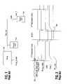
- FIG. 1illustrates a typical prior art charge pump circuit. It comprises a charge pump 100 that outputs regulated voltage V out — reg to a parasitic load 101 and a target load 103 .
- the parasitic load 103represents line capacitance of the pump output node.
- the target load 103is the capacitance of the connected word line to be programmed.
- Switch SW A 105is closed during the programming cycles to connect V out — reg to the target load 103 .
- FIG. 2illustrates a timing chart of a typical prior art non-volatile memory device such as the flash memory integrated circuit charge pump circuit of FIG. 1 .
- the timing chartshows that the I/O lines include the addresses, data, and commands for memory operation.
- a program enable signalgoes high.
- the program enable signalthen causes the charge pump enable signal to go high to initiate the pumping operation in order to precharge bit lines.
- FIG. 1shows a block diagram of a typical prior art charge pump circuit.
- FIG. 2shows a timing diagram of a typical prior art operation of the charge pump circuit of FIG. 1 .
- FIG. 3shows a portion of one embodiment of a NAND architecture flash memory array.
- FIG. 4shows an operational block diagram of one embodiment of a charge pump circuit of the present invention.
- FIG. 5shows a timing diagram of one embodiment of the operation of the charge pump circuit of FIG. 5 .
- FIG. 6shows a block diagram for one embodiment of a memory system of the present invention.
- FIG. 7shows a block diagram for one embodiment of a memory module of the present invention.
- FIG. 3illustrates a simplified diagram of a typical prior art NAND flash memory array.
- the memory array of FIG. 3does not show all of the elements typically required in a memory array. For example, only two bit lines are shown (BL 1 and BL 2 ) when the number of bit lines required actually depends upon the memory density.
- the arrayis comprised of an array of floating gate cells 301 arranged in series strings 304 , 305 .
- Each of the floating gate cells 301are coupled drain to source in each series chain 304 , 305 .
- a word line (WL 0 -WL 31 ) that spans across multiple series strings 304 , 305is coupled to the control gates of every floating gate cell in a row in order to control their operation.
- the bit lines BL 1 , BL 2are eventually coupled to sense amplifiers (not shown) that detect the state of each cell.
- the word linesselect the individual floating gate memory cells in the series chain 304 , 305 to be written to or read from and operate the remaining floating gate memory cells in each series string 304 , 305 in a pass through mode.
- Each series string 304 , 305 of floating gate memory cellsis coupled to a source line 306 by a source select gate 316 , 317 and to an individual bit line (BL 1 , BL 2 ) by a drain select gate 312 , 313 .
- the source select gates 316 , 317are controlled by a source select gate control line SG(S) 318 coupled to their control gates.
- the drain select gates 312 , 313are controlled by a drain select gate control line SG(D) 314 .
- a selected word line 300 for the flash memory cells 330 - 331 being programmedis typically biased by programming pulses that start at a voltage of around 16V and may incrementally increase to more than 20V.
- the unselected word lines for the remaining cellsare typically biased at V pass . This is typically in an approximate range of 9-10V.
- the bit lines of the cells to be programmedare typically biased at 0V while the inhibited bit lines are typically biased at V CC .
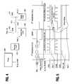
- FIG. 4illustrates an operational block diagram of one embodiment of the charge pump circuit of the present invention.
- the circuitis comprised of the charge pump device 400 that generates the V out — reg voltage for programming the memory cells. In one embodiment, this voltage is coupled to the word lines of the subsequently described non-volatile memory array.
- the parasitic load 401represents the total capacitance of the output line of the charge pump device 400 .
- the target load 403represents the load capacitance of the word line to which the charge pump device 400 is currently coupled for programming.
- the intentional load 405represents the load that is charged up during idle times to provide charge sharing with the target load.
- Switches SWA 411 , SWB 413 , and SWC 415provide the switching between the loads. In one embodiment, these switches 411 , 413 , 415 can be implemented using transistors.
- SWA 411couples the target load 403 to the pump 400 .
- SWB 413couples the intentional load 405 to the pump.
- SWC 415couples the intentional load 405 to the target load 403 .
- FIG. 5illustrates a timing diagram of one embodiment of the circuit of FIG. 4 .
- This diagramillustrates the I/Ox line that carries the desired operation commands (i.e., read, write, erase), the data to be programmed/read, and the address to which the data is to be written/read.
- desired operation commandsi.e., read, write, erase
- the PGM_ENABLE lineillustrates the state of the program enable signal to memory controller circuit to initiate the program operation. This signal also causes the memory controller to generate the PUMP_ENABLE signal. This signal is responsible for enabling the charge pump device 400 of FIG. 4 to begin the programming operation.
- V out — f signalrepresents the voltage on the target load as a result of the closing of SWC 415 .
- V out — reg signalis the voltage that is output from the pump 400 .
- V out — lis the voltage at the intentional load 405 .
- the SWA, SWB, and SWC linesrepresent the opening and closing of the switches 411 , 413 , 415 of FIG. 4 .
- the first program cycleis initiated by a program command or address load command on the I/Ox line.
- the illustrated commandis 80 H but this is for purposes of illustration only as the present invention is not limited to any one received command value or received command that is responsible for initiating the PGM_ENABLE.
- the received commandcauses the PGM_ENABLE line to go high to initiate the program operation.
- the PGM_ENABLE signalcauses the PUMP_ENABLE signal to go high and turn on the charge pump 400 .
- the charge pumpremains on during the data loading operation.
- V out — regstarts from 0V and rises to a target voltage with SWA closed.
- the target voltageis dependent on the embodiment and can be any voltage required for programming the memory cell (e.g. 20V). Since V out — reg sees the fixed loading capacitance of the target load 403 +parasitic load 401 , V out — reg rises with an RC time constant. Since SWA is closed, V out — f also tracks V out — reg . V out — l starts from 0V and rises to the target voltage with the closing of SWB 413 .
- V out — regreaches the target voltage
- the pump 400is idling (i.e., turned off or slowed down) with just enough output to maintain the V out — reg node at the target voltage. This compensates for junction leakage at the V out — reg node connections.
- SWB 413begins to open and close as shown in FIG. 5 . This charges the intentional load 405 .
- SWA 411 and SWB 413are clocking in an inverse pattern during the remainder of the first program cycle. SWA 411 is closing to compensate for leakage current by the target load 403 . SWB 413 is closing to charge the intentional node and to compensate for leakage current by the intentional load 405 .
- the PUMP_ENABLE signalremains high, SWA 411 is open, and SWB 413 remains closed. This provides a slow, weak charging to V out — l at the intentional load 405 .
- V out — fbegins to rise with the charge sharing initiated by closing SWC 415 .
- the initial slope of V out — f in the timing diagram of FIG. 5is the result of the charge sharing.
- SWC 415then opens and SWA 411 closes to couple the target load 403 to V out — reg to continue charging up V out — f .
- SWA 411 and SWB 413again clock on and off in an inverse fashion, as shown in the timing diagram, in order to compensate for the leakage current occurring in their respective loads 403 , 405 .
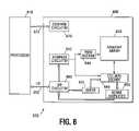
- FIG. 6illustrates a functional block diagram of a memory device 600 that can incorporate the embodiments for programming the non-volatile memory cells of the present invention.
- the memory device 600is coupled to a processor 610 .
- the processor 610may be a microprocessor or some other type of controlling circuitry.
- the memory device 600 and the processor 610form part of an electronic system 620 .
- the memory device 600has been simplified to focus on features of the memory that are helpful in understanding the present invention.
- the memory deviceincludes an array of flash memory cells 630 or some other type of non-volatile memory cells.
- the memory array 630is arranged in banks of rows and columns.
- the control gates of each row of memory cellsis coupled with a word line while the drain and source connections of the memory cells are coupled to bit lines.
- bit linesAs is well known in the art, the connection of the cells to the bit lines depends on whether the array is a NAND architecture, a NOR architecture, an AND architecture, or some other array architecture.
- An address buffer circuit 640is provided to latch address signals provided over I/O connections 662 through the I/O circuitry 660 . Address signals are received and decoded by row decoders 644 and column decoders 646 to access the memory array 630 . It will be appreciated by those skilled in the art that, with the benefit of the present description, the number of address input connections and row/column decoders depends on the density and architecture of the memory array 630 . That is, the number of addresses increases with both increased memory cell counts and increased bank and block counts.
- the memory integrated circuit 600reads data in the memory array 630 by sensing voltage or current changes in the memory array columns using sense/buffer circuitry 650 .
- the sense/buffer circuitryin one embodiment, is coupled to read and latch a row of data from the memory array 630 .
- Data input and output buffer circuitry 660is included for bi-directional data communication over the I/O connections 662 with the processor 610 .
- Write circuitry 655is provided to write data to the memory array.
- Control circuitry 670decodes signals provided on control connections 672 from the processor 610 . These signals are used to control the operations on the memory array 630 , including data read, data write, and erase operations.
- the control circuitry 670may be a state machine, a sequencer, or some other type of controller.
- the control circuitry 670 of the present inventionin one embodiment, is responsible for executing the embodiments of the programming method and charge pump control of the present invention.
- the flash memory device illustrated in FIG. 6has been simplified to facilitate a basic understanding of the features of the memory and is for purposes of illustration only. A more detailed understanding of internal circuitry and functions of flash memories are known to those skilled in the art. Alternate embodiments may include the flash memory cell of the present invention in other types of electronic systems.
- FIG. 7is an illustration of a memory module 700 that incorporates the memory cell embodiments as discussed previously.
- the memory module 700is illustrated as a memory card, the concepts discussed with reference to the memory module 700 are applicable to other types of removable or portable memory, e.g., USB flash drives.
- one example form factoris depicted in FIG. 7 , these concepts are applicable to other form factors as well.
- the memory module 700includes a housing 705 to enclose one or more memory devices 710 of the present invention.
- the housing 705includes one or more contacts 715 for communication with a host device. Examples of host devices include digital cameras, digital recording and playback devices, PDAs, personal computers, memory card readers, interface hubs and the like.
- the contacts 715are in the form of a standardized interface. For example, with a USB flash drive, the contacts 715 might be in the form of a USB Type-A male connector.
- the contacts 715are in the form of a semi-proprietary interface, such as might be found on COMPACTFLASH memory cards licensed by SANDISK Corporation, MEMORY STICK memory cards licensed by SONY Corporation, SD SECURE DIGITAL memory cards licensed by TOSHIBA Corporation and the like. In general, however, contacts 715 provide an interface for passing control, address and/or data signals between the memory module 700 and a host having compatible receptors for the contacts 715 .
- the memory module 700may optionally include additional circuitry 720 .
- the additional circuitry 720may include a memory controller for controlling access across multiple memory devices 710 and/or for providing a translation layer between an external host and a memory device 710 .
- a memory controllercould selectively couple an I/O connection (not shown in FIG. 7 ) of a memory device 710 to receive the appropriate signal at the appropriate I/O connection at the appropriate time or to provide the appropriate signal at the appropriate contact 715 at the appropriate time.
- the communication protocol between a host and the memory module 700may be different than what is required for access of a memory device 710 .
- a memory controllercould then translate the command sequences received from a host into the appropriate command sequences to achieve the desired access to the memory device 710 .
- Such translationmay further include changes in signal voltage levels in addition to command sequences.
- the additional circuitry 720may further include functionality unrelated to control of a memory device 710 .
- the additional circuitry 720may include circuitry to restrict read or write access to the memory module 700 , such as password protection, biometrics or the like.
- the additional circuitry 720may include circuitry to indicate a status of the memory module 700 .
- the additional circuitry 720may include functionality to determine whether power is being supplied to the memory module 700 and whether the memory module 700 is currently being accessed, and to display an indication of its status, such as a solid light while powered and a flashing light while being accessed.
- the additional circuitry 720may further include passive devices, such as decoupling capacitors to help regulate power requirements within the memory module 700 .
- the embodiments of the present inventionprovide stable memory device operation and reduced program time by enabling the charge pump at some point prior to the data load instead of after the data load, as in the prior art. This minimizes the pump driving current during the program cycle start in order to reduce the supply peak current, thus providing stable device operation. Additionally, an intentional load provides charge sharing to reduce the load on the regulated voltage output from the pump during program cycle start.
Landscapes
- Engineering & Computer Science (AREA)
- Power Engineering (AREA)
- Read Only Memory (AREA)
Abstract
Description
- The present invention relates generally to memory devices and in particular the present invention relates to non-volatile memory devices.
- Memory devices are typically provided as internal, semiconductor, integrated circuits in computers or other electronic devices. There are many different types of memory including random-access memory (RAM), read only memory (ROM), dynamic random access memory (DRAM), synchronous dynamic random access memory (SDRAM), and flash memory.
- Flash memory devices have developed into a popular source of non-volatile memory for a wide range of electronic applications. Flash memory devices typically use a one-transistor memory cell that allows for high memory densities, high reliability, and low power consumption. Common uses for flash memory include personal computers, personal digital assistants (PDAs), digital cameras, and cellular telephones. Program code and system data such as a basic input/output system (BIOS) are typically stored in flash memory devices for use in personal computer systems.
- A charge pump circuit is used in a non-volatile memory device to generate the voltages required for chip operation. A charge pump is an electronic circuit that uses capacitors as energy storage elements to convert DC voltages into other DC voltages.
- A typical charge pump uses transistors to control the operation of the pump and connection of voltages to the capacitors. For instance, a typical prior art charge pump can generate a higher voltage through multiple stages. A first stage involves a capacitor being connected across a voltage and charged up. In a second stage, the capacitor is disconnected from the original charging voltage and reconnected with its negative terminal to the original positive charging voltage. Because the capacitor mostly retains the voltage across it, except for leakage, the positive terminal voltage is added to the original, effectively doubling the voltage. The pulsing nature of the higher voltage output is typically smoothed by the use of another capacitor at the output.
FIG. 1 illustrates a typical prior art charge pump circuit. It comprises acharge pump 100 that outputs regulated voltage Vout— regto aparasitic load 101 and atarget load 103. Theparasitic load 103 represents line capacitance of the pump output node. Thetarget load 103 is the capacitance of the connected word line to be programmed. Switch SWA105 is closed during the programming cycles to connect Vout— regto thetarget load 103.FIG. 2 illustrates a timing chart of a typical prior art non-volatile memory device such as the flash memory integrated circuit charge pump circuit ofFIG. 1 . The timing chart shows that the I/O lines include the addresses, data, and commands for memory operation.- Referring to
FIG. 2 , when the command for a program operation is received (e.g.,10H), a program enable signal goes high. The program enable signal then causes the charge pump enable signal to go high to initiate the pumping operation in order to precharge bit lines. - One problem with this charge pump operation is that the operation of the pump circuits causes noise on the bit lines. This can cause problems with programming of the cells that are coupled to the bit lines experiencing the noise. Additionally, a fast pump turn-on creates a peak current that causes a
downward spike 200 in the supply voltage (VCC) as illustrated inFIG. 2 . This can result in unstable memory device operation. - For the reasons stated above, and for other reasons stated below which will become apparent to those skilled in the art upon reading and understanding the present specification, there is a need in the art for more efficient use of charge pumps in a non-volatile memory device.
FIG. 1 shows a block diagram of a typical prior art charge pump circuit.FIG. 2 shows a timing diagram of a typical prior art operation of the charge pump circuit ofFIG. 1 .FIG. 3 shows a portion of one embodiment of a NAND architecture flash memory array.FIG. 4 shows an operational block diagram of one embodiment of a charge pump circuit of the present invention.FIG. 5 shows a timing diagram of one embodiment of the operation of the charge pump circuit ofFIG. 5 .FIG. 6 shows a block diagram for one embodiment of a memory system of the present invention.FIG. 7 shows a block diagram for one embodiment of a memory module of the present invention.- In the following detailed description of the invention, reference is made to the accompanying drawings that form a part hereof and in which is shown, by way of illustration, specific embodiments in which the invention may be practiced. In the drawings, like numerals describe substantially similar components throughout the several views. These embodiments are described in sufficient detail to enable those skilled in the art to practice the invention. Other embodiments may be utilized and structural, logical, and electrical changes may be made without departing from the scope of the present invention. The following detailed description is, therefore, not to be taken in a limiting sense, and the scope of the present invention is defined only by the appended claims and equivalents thereof.
FIG. 3 illustrates a simplified diagram of a typical prior art NAND flash memory array. The memory array ofFIG. 3 , for purposes of clarity, does not show all of the elements typically required in a memory array. For example, only two bit lines are shown (BL1 and BL2) when the number of bit lines required actually depends upon the memory density.- The array is comprised of an array of floating
gate cells 301 arranged inseries strings floating gate cells 301 are coupled drain to source in eachseries chain multiple series strings - In operation, the word lines (WL0-WL31) select the individual floating gate memory cells in the
series chain series string series string source line 306 by a sourceselect gate select gate gates select gates - A
selected word line 300 for the flash memory cells330-331 being programmed is typically biased by programming pulses that start at a voltage of around 16V and may incrementally increase to more than 20V. The unselected word lines for the remaining cells are typically biased at Vpass. This is typically in an approximate range of 9-10V. The bit lines of the cells to be programmed are typically biased at 0V while the inhibited bit lines are typically biased at VCC. FIG. 4 illustrates an operational block diagram of one embodiment of the charge pump circuit of the present invention. The circuit is comprised of thecharge pump device 400 that generates the Vout— regvoltage for programming the memory cells. In one embodiment, this voltage is coupled to the word lines of the subsequently described non-volatile memory array.- The
parasitic load 401 represents the total capacitance of the output line of thecharge pump device 400. Thetarget load 403 represents the load capacitance of the word line to which thecharge pump device 400 is currently coupled for programming. Theintentional load 405 represents the load that is charged up during idle times to provide charge sharing with the target load. Switches SWA 411,SWB 413, andSWC 415 provide the switching between the loads. In one embodiment, theseswitches SWA 411 couples thetarget load 403 to thepump 400.SWB 413 couples theintentional load 405 to the pump.SWC 415 couples theintentional load 405 to thetarget load 403.FIG. 5 illustrates a timing diagram of one embodiment of the circuit ofFIG. 4 . This diagram illustrates the I/Ox line that carries the desired operation commands (i.e., read, write, erase), the data to be programmed/read, and the address to which the data is to be written/read.- The PGM_ENABLE line illustrates the state of the program enable signal to memory controller circuit to initiate the program operation. This signal also causes the memory controller to generate the PUMP_ENABLE signal. This signal is responsible for enabling the
charge pump device 400 ofFIG. 4 to begin the programming operation. - The Vout
— fsignal represents the voltage on the target load as a result of the closing ofSWC 415. Vout— regsignal is the voltage that is output from thepump 400. Vout— lis the voltage at theintentional load 405. The SWA, SWB, and SWC lines represent the opening and closing of theswitches FIG. 4 . - In operation, the first program cycle is initiated by a program command or address load command on the I/Ox line. The illustrated command is80H but this is for purposes of illustration only as the present invention is not limited to any one received command value or received command that is responsible for initiating the PGM_ENABLE. The received command causes the PGM_ENABLE line to go high to initiate the program operation. The PGM_ENABLE signal causes the PUMP_ENABLE signal to go high and turn on the
charge pump 400. The charge pump remains on during the data loading operation. - Vout
— regstarts from 0V and rises to a target voltage with SWA closed. The target voltage is dependent on the embodiment and can be any voltage required for programming the memory cell (e.g. 20V). Since Vout— regsees the fixed loading capacitance of thetarget load 403+parasitic load 401, Vout— regrises with an RC time constant. Since SWA is closed, Vout— falso tracks Vout— reg. Vout— lstarts from 0V and rises to the target voltage with the closing ofSWB 413. - Once Vout
— regreaches the target voltage, thepump 400 is idling (i.e., turned off or slowed down) with just enough output to maintain the Vout— regnode at the target voltage. This compensates for junction leakage at the Vout— regnode connections. SWB 413 begins to open and close as shown inFIG. 5 . This charges theintentional load 405. As can be seen in the timing diagram,SWA 411 andSWB 413 are clocking in an inverse pattern during the remainder of the first program cycle.SWA 411 is closing to compensate for leakage current by thetarget load 403.SWB 413 is closing to charge the intentional node and to compensate for leakage current by theintentional load 405.- During the verify cycle, the PUMP_ENABLE signal remains high,
SWA 411 is open, andSWB 413 remains closed. This provides a slow, weak charging to Vout— lat theintentional load 405. - During the second program cycle, PUMP_ENABLE remains high. The stored charge in the
intentional load 405 is then used to charge up thetarget load 403 by charge sharing. This is accomplished by closingSWC 415 as shown inFIG. 5 . BothSWA 411 andSWB 413 are open whenSWC 415 momentarily closes. The charge sharing between Vout— land Vout— fcauses only a minor downward spike in the Vout— regsignal that is substantially reduced from the prior art. The peak reduction results in substantially more stable memory device operation. - The Vout
— fsignal begins to rise with the charge sharing initiated by closingSWC 415. The initial slope of Vout— fin the timing diagram ofFIG. 5 is the result of the charge sharing.SWC 415 then opens andSWA 411 closes to couple thetarget load 403 to Vout— regto continue charging up Vout— f. For the remainder of the second program cycle,SWA 411 andSWB 413 again clock on and off in an inverse fashion, as shown in the timing diagram, in order to compensate for the leakage current occurring in theirrespective loads FIG. 6 illustrates a functional block diagram of amemory device 600 that can incorporate the embodiments for programming the non-volatile memory cells of the present invention. Thememory device 600 is coupled to aprocessor 610. Theprocessor 610 may be a microprocessor or some other type of controlling circuitry. Thememory device 600 and theprocessor 610 form part of anelectronic system 620. Thememory device 600 has been simplified to focus on features of the memory that are helpful in understanding the present invention.- The memory device includes an array of
flash memory cells 630 or some other type of non-volatile memory cells. Thememory array 630 is arranged in banks of rows and columns. The control gates of each row of memory cells is coupled with a word line while the drain and source connections of the memory cells are coupled to bit lines. As is well known in the art, the connection of the cells to the bit lines depends on whether the array is a NAND architecture, a NOR architecture, an AND architecture, or some other array architecture. - An
address buffer circuit 640 is provided to latch address signals provided over I/O connections 662 through the I/O circuitry 660. Address signals are received and decoded byrow decoders 644 andcolumn decoders 646 to access thememory array 630. It will be appreciated by those skilled in the art that, with the benefit of the present description, the number of address input connections and row/column decoders depends on the density and architecture of thememory array 630. That is, the number of addresses increases with both increased memory cell counts and increased bank and block counts. - The memory integrated
circuit 600 reads data in thememory array 630 by sensing voltage or current changes in the memory array columns using sense/buffer circuitry 650. The sense/buffer circuitry, in one embodiment, is coupled to read and latch a row of data from thememory array 630. Data input andoutput buffer circuitry 660 is included for bi-directional data communication over the I/O connections 662 with theprocessor 610. Writecircuitry 655 is provided to write data to the memory array. Control circuitry 670 decodes signals provided oncontrol connections 672 from theprocessor 610. These signals are used to control the operations on thememory array 630, including data read, data write, and erase operations. Thecontrol circuitry 670 may be a state machine, a sequencer, or some other type of controller. Thecontrol circuitry 670 of the present invention, in one embodiment, is responsible for executing the embodiments of the programming method and charge pump control of the present invention.- The flash memory device illustrated in
FIG. 6 has been simplified to facilitate a basic understanding of the features of the memory and is for purposes of illustration only. A more detailed understanding of internal circuitry and functions of flash memories are known to those skilled in the art. Alternate embodiments may include the flash memory cell of the present invention in other types of electronic systems. FIG. 7 is an illustration of amemory module 700 that incorporates the memory cell embodiments as discussed previously. Although thememory module 700 is illustrated as a memory card, the concepts discussed with reference to thememory module 700 are applicable to other types of removable or portable memory, e.g., USB flash drives. In addition, although one example form factor is depicted inFIG. 7 , these concepts are applicable to other form factors as well.- The
memory module 700 includes ahousing 705 to enclose one ormore memory devices 710 of the present invention. Thehousing 705 includes one ormore contacts 715 for communication with a host device. Examples of host devices include digital cameras, digital recording and playback devices, PDAs, personal computers, memory card readers, interface hubs and the like. For some embodiment, thecontacts 715 are in the form of a standardized interface. For example, with a USB flash drive, thecontacts 715 might be in the form of a USB Type-A male connector. For some embodiments, thecontacts 715 are in the form of a semi-proprietary interface, such as might be found on COMPACTFLASH memory cards licensed by SANDISK Corporation, MEMORY STICK memory cards licensed by SONY Corporation, SD SECURE DIGITAL memory cards licensed by TOSHIBA Corporation and the like. In general, however,contacts 715 provide an interface for passing control, address and/or data signals between thememory module 700 and a host having compatible receptors for thecontacts 715. - The
memory module 700 may optionally includeadditional circuitry 720. For some embodiments, theadditional circuitry 720 may include a memory controller for controlling access acrossmultiple memory devices 710 and/or for providing a translation layer between an external host and amemory device 710. For example, there may not be a one-to-one correspondence between the number ofcontacts 715 and a number of I/O connections to the one ormore memory devices 710. Thus, a memory controller could selectively couple an I/O connection (not shown inFIG. 7 ) of amemory device 710 to receive the appropriate signal at the appropriate I/O connection at the appropriate time or to provide the appropriate signal at theappropriate contact 715 at the appropriate time. Similarly, the communication protocol between a host and thememory module 700 may be different than what is required for access of amemory device 710. A memory controller could then translate the command sequences received from a host into the appropriate command sequences to achieve the desired access to thememory device 710. Such translation may further include changes in signal voltage levels in addition to command sequences. - The
additional circuitry 720 may further include functionality unrelated to control of amemory device 710. Theadditional circuitry 720 may include circuitry to restrict read or write access to thememory module 700, such as password protection, biometrics or the like. Theadditional circuitry 720 may include circuitry to indicate a status of thememory module 700. For example, theadditional circuitry 720 may include functionality to determine whether power is being supplied to thememory module 700 and whether thememory module 700 is currently being accessed, and to display an indication of its status, such as a solid light while powered and a flashing light while being accessed. Theadditional circuitry 720 may further include passive devices, such as decoupling capacitors to help regulate power requirements within thememory module 700. - In summary, the embodiments of the present invention provide stable memory device operation and reduced program time by enabling the charge pump at some point prior to the data load instead of after the data load, as in the prior art. This minimizes the pump driving current during the program cycle start in order to reduce the supply peak current, thus providing stable device operation. Additionally, an intentional load provides charge sharing to reduce the load on the regulated voltage output from the pump during program cycle start.
- Although specific embodiments have been illustrated and described herein, it will be appreciated by those of ordinary skill in the art that any arrangement that is calculated to achieve the same purpose may be substituted for the specific embodiments shown. Many adaptations of the invention will be apparent to those of ordinary skill in the art. Accordingly, this application is intended to cover any adaptations or variations of the invention. It is manifestly intended that this invention be limited only by the following claims and equivalents thereof.
Claims (34)
Priority Applications (4)
| Application Number | Priority Date | Filing Date | Title |
|---|---|---|---|
| US11/451,822US7626865B2 (en) | 2006-06-13 | 2006-06-13 | Charge pump operation in a non-volatile memory device |
| US12/627,077US8000152B2 (en) | 2006-06-13 | 2009-11-30 | Charge pump operation in a non-volatile memory device |
| US13/186,766US8194466B2 (en) | 2006-06-13 | 2011-07-20 | Charge pump operation in a non-volatile memory device |
| US13/471,778US8547754B2 (en) | 2006-06-13 | 2012-05-15 | Charge pump operation in a non-volatile memory device |
Applications Claiming Priority (1)
| Application Number | Priority Date | Filing Date | Title |
|---|---|---|---|
| US11/451,822US7626865B2 (en) | 2006-06-13 | 2006-06-13 | Charge pump operation in a non-volatile memory device |
Related Child Applications (1)
| Application Number | Title | Priority Date | Filing Date |
|---|---|---|---|
| US12/627,077DivisionUS8000152B2 (en) | 2006-06-13 | 2009-11-30 | Charge pump operation in a non-volatile memory device |
Publications (2)
| Publication Number | Publication Date |
|---|---|
| US20070291547A1true US20070291547A1 (en) | 2007-12-20 |
| US7626865B2 US7626865B2 (en) | 2009-12-01 |
Family
ID=38861379
Family Applications (4)
| Application Number | Title | Priority Date | Filing Date |
|---|---|---|---|
| US11/451,822Active2027-10-14US7626865B2 (en) | 2006-06-13 | 2006-06-13 | Charge pump operation in a non-volatile memory device |
| US12/627,077ActiveUS8000152B2 (en) | 2006-06-13 | 2009-11-30 | Charge pump operation in a non-volatile memory device |
| US13/186,766ActiveUS8194466B2 (en) | 2006-06-13 | 2011-07-20 | Charge pump operation in a non-volatile memory device |
| US13/471,778ActiveUS8547754B2 (en) | 2006-06-13 | 2012-05-15 | Charge pump operation in a non-volatile memory device |
Family Applications After (3)
| Application Number | Title | Priority Date | Filing Date |
|---|---|---|---|
| US12/627,077ActiveUS8000152B2 (en) | 2006-06-13 | 2009-11-30 | Charge pump operation in a non-volatile memory device |
| US13/186,766ActiveUS8194466B2 (en) | 2006-06-13 | 2011-07-20 | Charge pump operation in a non-volatile memory device |
| US13/471,778ActiveUS8547754B2 (en) | 2006-06-13 | 2012-05-15 | Charge pump operation in a non-volatile memory device |
Country Status (1)
| Country | Link |
|---|---|
| US (4) | US7626865B2 (en) |
Cited By (3)
| Publication number | Priority date | Publication date | Assignee | Title |
|---|---|---|---|---|
| CN111785308A (en)* | 2020-06-10 | 2020-10-16 | 深圳市芯天下技术有限公司 | Method, system, storage medium and terminal for reducing area of non-flash memory programming pump |
| CN114664352A (en)* | 2020-12-23 | 2022-06-24 | 华邦电子股份有限公司 | Memory circuit and memory programming method |
| CN115440280A (en)* | 2021-06-01 | 2022-12-06 | 美光科技公司 | Power management |
Families Citing this family (7)
| Publication number | Priority date | Publication date | Assignee | Title |
|---|---|---|---|---|
| US7626865B2 (en)* | 2006-06-13 | 2009-12-01 | Micron Technology, Inc. | Charge pump operation in a non-volatile memory device |
| US8300489B2 (en) | 2010-01-12 | 2012-10-30 | International Business Machines Corporation | Charge pump system and method utilizing adjustable output charge and compilation system and method for use by the charge pump |
| US20160006348A1 (en) | 2014-07-07 | 2016-01-07 | Ememory Technology Inc. | Charge pump apparatus |
| KR20170014197A (en)* | 2015-07-29 | 2017-02-08 | 에스케이하이닉스 주식회사 | Nonvolatile memory device, nonvolatile memory system and method for operating nonvolatile memory device |
| JP6535784B1 (en) | 2018-04-25 | 2019-06-26 | ウィンボンド エレクトロニクス コーポレーション | Semiconductor memory device |
| US11087849B2 (en)* | 2018-05-08 | 2021-08-10 | Sandisk Technologies Llc | Non-volatile memory with bit line controlled multi-plane mixed sub-block programming |
| US12224011B2 (en) | 2022-04-22 | 2025-02-11 | SanDisk Technologies, Inc. | Non-volatile memory with concurrent sub-block programming |
Citations (28)
| Publication number | Priority date | Publication date | Assignee | Title |
|---|---|---|---|---|
| US5740109A (en)* | 1996-08-23 | 1998-04-14 | Motorola, Inc. | Non-linear charge pump |
| US5945870A (en)* | 1996-07-18 | 1999-08-31 | Altera Corporation | Voltage ramp rate control circuit |
| US6259635B1 (en)* | 1999-01-19 | 2001-07-10 | Stmicroelectronics S.R.L. | Capacitive boosting circuit for the regulation of the word line reading voltage in non-volatile memories |
| US6259632B1 (en)* | 1999-01-19 | 2001-07-10 | Stmicroelectronics S.R.L. | Capacitive compensation circuit for the regulation of the word line reading voltage in non-volatile memories |
| US6278639B1 (en)* | 1998-09-08 | 2001-08-21 | Kabushiki Kaisha Toshiba | Booster circuit having booster cell sections connected in parallel, voltage generating circuit and semiconductor memory which use such booster circuit |
| US6356469B1 (en)* | 2000-09-14 | 2002-03-12 | Fairchild Semiconductor Corporation | Low voltage charge pump employing optimized clock amplitudes |
| US6385065B1 (en)* | 2000-09-14 | 2002-05-07 | Fairchild Semiconductor Corporation | Low voltage charge pump employing distributed charge boosting |
| US6438032B1 (en)* | 2001-03-27 | 2002-08-20 | Micron Telecommunications, Inc. | Non-volatile memory with peak current noise reduction |
| US6480436B2 (en)* | 2000-07-26 | 2002-11-12 | Stmicroelectronics S.R.L. | Non-volatile memory with a charge pump with regulated voltage |
| US6498761B2 (en)* | 1997-02-27 | 2002-12-24 | Kabushiki Kaisha Toshiba | Power supply circuit and semiconductor memory device having the same |
| US6518828B2 (en)* | 2000-12-18 | 2003-02-11 | Hynix Semiconductor Inc. | Pumping voltage regulation circuit |
| US6538930B2 (en)* | 2001-01-09 | 2003-03-25 | Mitsubishi Denki Kabushiki Kaisha | Charge pump circuit for generating positive and negative voltage with reverse current prevention circuit and a nonvolatile memory using the same |
| US6560145B2 (en)* | 2001-02-06 | 2003-05-06 | Ignazio Martines | Charge pump for a nonvolatile memory with read voltage regulation in the presence of address skew, and nonvolatile memory comprising such a charge pump |
| US6573780B2 (en)* | 1999-02-02 | 2003-06-03 | Macronix International Co., Ltd. | Four-phase charge pump with lower peak current |
| US6661682B2 (en)* | 2001-02-16 | 2003-12-09 | Imec (Interuniversitair Microelectronica Centrum) | High voltage generating charge pump circuit |
| US6683488B2 (en)* | 2000-12-30 | 2004-01-27 | Hynix Semiconductor, Inc. | Charge pump circuit for semiconductor device |
| US6735118B2 (en)* | 2001-07-06 | 2004-05-11 | Halo Lsi, Inc. | CG-WL voltage boosting scheme for twin MONOS |
| US6765428B2 (en)* | 2000-12-30 | 2004-07-20 | Hynix Semiconductor, Inc. | Charge pump device for semiconductor memory |
| US6785180B2 (en)* | 2001-03-15 | 2004-08-31 | Micron Technology, Inc. | Programmable soft-start control for charge pump |
| US6788578B1 (en)* | 2003-01-27 | 2004-09-07 | Turbo Ic, Inc. | Charge pump for conductive lines in programmable memory array |
| US6801455B2 (en)* | 2002-09-11 | 2004-10-05 | Seiko Epson Corporation | Voltage generation circuit for non-volatile semiconductor memory device |
| US20050057236A1 (en)* | 2003-09-17 | 2005-03-17 | Nicola Telecco | Dual stage voltage regulation circuit |
| US6912172B2 (en)* | 2001-06-14 | 2005-06-28 | Hitachi, Ltd. | Semiconductor device and method of the semiconductor device |
| US6933768B2 (en)* | 2002-06-20 | 2005-08-23 | Infineon Technologies Ag | Method for increasing the input voltage of an integrated circuit with a two-stage charge pump, and integrated circuit |
| US6937517B2 (en)* | 2002-07-18 | 2005-08-30 | Micron Technology, Inc. | Clock regulation scheme for varying loads |
| US7274602B2 (en)* | 2005-05-30 | 2007-09-25 | Spansion Llc | Storage device and control method therefor |
| US7385377B2 (en)* | 2004-10-28 | 2008-06-10 | Stmicroelectronics, S.R.L. | Voltage down-converter with reduced ripple |
| US7439797B2 (en)* | 2006-09-28 | 2008-10-21 | Samsung Electronics Co., Ltd. | Semiconductor device including a high voltage generation circuit and method of generating a high voltage |
Family Cites Families (43)
| Publication number | Priority date | Publication date | Assignee | Title |
|---|---|---|---|---|
| US4823317A (en)* | 1988-01-20 | 1989-04-18 | Ict International Cmos Technolgy, Inc. | EEPROM programming switch |
| US4831589A (en)* | 1988-01-20 | 1989-05-16 | Ict International Cmos Technology, Inc. | EEPROM programming switch operable at low VCC |
| US5038325A (en)* | 1990-03-26 | 1991-08-06 | Micron Technology Inc. | High efficiency charge pump circuit |
| KR940002859B1 (en)* | 1991-03-14 | 1994-04-04 | 삼성전자 주식회사 | Wordline driver circuit in semiconductor memory device |
| US5255224A (en)* | 1991-12-18 | 1993-10-19 | International Business Machines Corporation | Boosted drive system for master/local word line memory architecture |
| US5442586A (en)* | 1993-09-10 | 1995-08-15 | Intel Corporation | Method and apparatus for controlling the output current provided by a charge pump circuit |
| US5537350A (en)* | 1993-09-10 | 1996-07-16 | Intel Corporation | Method and apparatus for sequential programming of the bits in a word of a flash EEPROM memory array |
| US5680300A (en)* | 1995-12-22 | 1997-10-21 | Analog Devices, Inc. | Regulated charge pump DC/DC converter |
| KR0176115B1 (en)* | 1996-05-15 | 1999-04-15 | 김광호 | Charge Pump Circuit in Nonvolatile Semiconductor Memory Devices |
| JP3384521B2 (en)* | 1996-06-07 | 2003-03-10 | 矢崎総業株式会社 | Switching device |
| US5943263A (en)* | 1997-01-08 | 1999-08-24 | Micron Technology, Inc. | Apparatus and method for programming voltage protection in a non-volatile memory system |
| JP3346273B2 (en)* | 1998-04-24 | 2002-11-18 | 日本電気株式会社 | Boost circuit and semiconductor memory device |
| JP3248576B2 (en)* | 1998-10-05 | 2002-01-21 | 日本電気株式会社 | Boost circuit and boost method |
| JP3713401B2 (en)* | 1999-03-18 | 2005-11-09 | 株式会社東芝 | Charge pump circuit |
| US6310789B1 (en)* | 1999-06-25 | 2001-10-30 | The Procter & Gamble Company | Dynamically-controlled, intrinsically regulated charge pump power converter |
| US6166960A (en)* | 1999-09-24 | 2000-12-26 | Microchip Technology, Incorporated | Method, system and apparatus for determining that a programming voltage level is sufficient for reliably programming an eeprom |
| US6522558B2 (en)* | 2000-06-13 | 2003-02-18 | Linfinity Microelectronics | Single mode buck/boost regulating charge pump |
| US6233177B1 (en)* | 2000-06-22 | 2001-05-15 | Xilinx, Inc. | Bitline latch switching circuit for floating gate memory device requiring zero volt programming voltage |
| IT1318158B1 (en)* | 2000-07-13 | 2003-07-23 | St Microelectronics Srl | CIRCUIT DEVICE TO MAKE A HIERARCHICAL DECODING DIRECT IN NON-VOLATILE MEMORY DEVICES. |
| EP1202427B1 (en)* | 2000-10-27 | 2013-08-28 | Invensys Systems, Inc. | Load voltage controller for a field device and related control method |
| JP3875020B2 (en)* | 2000-12-26 | 2007-01-31 | アルプス電気株式会社 | Method for manufacturing perpendicular magnetic recording head |
| US6535424B2 (en)* | 2001-07-25 | 2003-03-18 | Advanced Micro Devices, Inc. | Voltage boost circuit using supply voltage detection to compensate for supply voltage variations in read mode voltage |
| US6445623B1 (en)* | 2001-08-22 | 2002-09-03 | Texas Instruments Incorporated | Charge pumps with current sources for regulation |
| US6618296B2 (en)* | 2001-08-22 | 2003-09-09 | Texas Instruments Incorporated | Charge pump with controlled charge current |
| JP4834261B2 (en)* | 2001-09-27 | 2011-12-14 | Okiセミコンダクタ株式会社 | Boost power supply generation circuit |
| US6657875B1 (en)* | 2002-07-16 | 2003-12-02 | Fairchild Semiconductor Corporation | Highly efficient step-down/step-up and step-up/step-down charge pump |
| JP2004064937A (en)* | 2002-07-31 | 2004-02-26 | Nec Corp | Charge pump-type boosting circuit |
| ITMI20022268A1 (en)* | 2002-10-25 | 2004-04-26 | Atmel Corp | VARIABLE CHARGE PUMP CIRCUIT WITH DYNAMIC LOAD |
| US6822884B1 (en)* | 2003-05-22 | 2004-11-23 | Analog Microelectronics, Inc. | Pulse width modulated charge pump |
| JP2005151777A (en)* | 2003-11-19 | 2005-06-09 | Sanyo Electric Co Ltd | Charge pumping circuit and amplifier |
| JP4301027B2 (en)* | 2004-02-13 | 2009-07-22 | 株式会社デンソー | Voltage output adjusting device and voltage output adjusting method |
| JP4377274B2 (en)* | 2004-03-26 | 2009-12-02 | Necエレクトロニクス株式会社 | Power supply circuit and semiconductor memory device provided with the power supply circuit |
| DE102004028934B3 (en)* | 2004-06-15 | 2006-01-05 | Infineon Technologies Ag | Discharge circuit for a capacitive load |
| US7256640B2 (en)* | 2005-01-03 | 2007-08-14 | Stmicroelectronics S.R.L. | Multi-stage charge pump voltage generator with protection of the devices of the charge pump |
| US7375992B2 (en)* | 2005-01-24 | 2008-05-20 | The Hong Kong University Of Science And Technology | Switched-capacitor regulators |
| US7248521B2 (en)* | 2005-07-12 | 2007-07-24 | Micron Technology, Inc. | Negative voltage discharge scheme to improve snapback in a non-volatile memory |
| TWI315456B (en)* | 2005-07-21 | 2009-10-01 | Novatek Microelectronics Corp | Charge pump control circuit |
| US7352626B1 (en)* | 2005-08-29 | 2008-04-01 | Spansion Llc | Voltage regulator with less overshoot and faster settling time |
| US7626865B2 (en)* | 2006-06-13 | 2009-12-01 | Micron Technology, Inc. | Charge pump operation in a non-volatile memory device |
| US7599231B2 (en)* | 2006-10-11 | 2009-10-06 | Atmel Corporation | Adaptive regulator for idle state in a charge pump circuit of a memory device |
| GB2444984B (en)* | 2006-12-22 | 2011-07-13 | Wolfson Microelectronics Plc | Charge pump circuit and methods of operation thereof |
| US7443735B2 (en)* | 2006-12-22 | 2008-10-28 | Sandisk Corporation | Method of reducing wordline recovery time |
| US8044705B2 (en)* | 2007-08-28 | 2011-10-25 | Sandisk Technologies Inc. | Bottom plate regulation of charge pumps |
- 2006
- 2006-06-13USUS11/451,822patent/US7626865B2/enactiveActive
- 2009
- 2009-11-30USUS12/627,077patent/US8000152B2/enactiveActive
- 2011
- 2011-07-20USUS13/186,766patent/US8194466B2/enactiveActive
- 2012
- 2012-05-15USUS13/471,778patent/US8547754B2/enactiveActive
Patent Citations (29)
| Publication number | Priority date | Publication date | Assignee | Title |
|---|---|---|---|---|
| US5945870A (en)* | 1996-07-18 | 1999-08-31 | Altera Corporation | Voltage ramp rate control circuit |
| US5740109A (en)* | 1996-08-23 | 1998-04-14 | Motorola, Inc. | Non-linear charge pump |
| US6498761B2 (en)* | 1997-02-27 | 2002-12-24 | Kabushiki Kaisha Toshiba | Power supply circuit and semiconductor memory device having the same |
| US6278639B1 (en)* | 1998-09-08 | 2001-08-21 | Kabushiki Kaisha Toshiba | Booster circuit having booster cell sections connected in parallel, voltage generating circuit and semiconductor memory which use such booster circuit |
| US6259635B1 (en)* | 1999-01-19 | 2001-07-10 | Stmicroelectronics S.R.L. | Capacitive boosting circuit for the regulation of the word line reading voltage in non-volatile memories |
| US6259632B1 (en)* | 1999-01-19 | 2001-07-10 | Stmicroelectronics S.R.L. | Capacitive compensation circuit for the regulation of the word line reading voltage in non-volatile memories |
| US6573780B2 (en)* | 1999-02-02 | 2003-06-03 | Macronix International Co., Ltd. | Four-phase charge pump with lower peak current |
| US6480436B2 (en)* | 2000-07-26 | 2002-11-12 | Stmicroelectronics S.R.L. | Non-volatile memory with a charge pump with regulated voltage |
| US6385065B1 (en)* | 2000-09-14 | 2002-05-07 | Fairchild Semiconductor Corporation | Low voltage charge pump employing distributed charge boosting |
| US6356469B1 (en)* | 2000-09-14 | 2002-03-12 | Fairchild Semiconductor Corporation | Low voltage charge pump employing optimized clock amplitudes |
| US6633494B2 (en)* | 2000-09-14 | 2003-10-14 | Fairchild Semiconductor Corporation | Low voltage charge pump employing distributed charge boosting |
| US6518828B2 (en)* | 2000-12-18 | 2003-02-11 | Hynix Semiconductor Inc. | Pumping voltage regulation circuit |
| US6765428B2 (en)* | 2000-12-30 | 2004-07-20 | Hynix Semiconductor, Inc. | Charge pump device for semiconductor memory |
| US6683488B2 (en)* | 2000-12-30 | 2004-01-27 | Hynix Semiconductor, Inc. | Charge pump circuit for semiconductor device |
| US6538930B2 (en)* | 2001-01-09 | 2003-03-25 | Mitsubishi Denki Kabushiki Kaisha | Charge pump circuit for generating positive and negative voltage with reverse current prevention circuit and a nonvolatile memory using the same |
| US6560145B2 (en)* | 2001-02-06 | 2003-05-06 | Ignazio Martines | Charge pump for a nonvolatile memory with read voltage regulation in the presence of address skew, and nonvolatile memory comprising such a charge pump |
| US6661682B2 (en)* | 2001-02-16 | 2003-12-09 | Imec (Interuniversitair Microelectronica Centrum) | High voltage generating charge pump circuit |
| US6785180B2 (en)* | 2001-03-15 | 2004-08-31 | Micron Technology, Inc. | Programmable soft-start control for charge pump |
| US6438032B1 (en)* | 2001-03-27 | 2002-08-20 | Micron Telecommunications, Inc. | Non-volatile memory with peak current noise reduction |
| US6912172B2 (en)* | 2001-06-14 | 2005-06-28 | Hitachi, Ltd. | Semiconductor device and method of the semiconductor device |
| US6735118B2 (en)* | 2001-07-06 | 2004-05-11 | Halo Lsi, Inc. | CG-WL voltage boosting scheme for twin MONOS |
| US6933768B2 (en)* | 2002-06-20 | 2005-08-23 | Infineon Technologies Ag | Method for increasing the input voltage of an integrated circuit with a two-stage charge pump, and integrated circuit |
| US6937517B2 (en)* | 2002-07-18 | 2005-08-30 | Micron Technology, Inc. | Clock regulation scheme for varying loads |
| US6801455B2 (en)* | 2002-09-11 | 2004-10-05 | Seiko Epson Corporation | Voltage generation circuit for non-volatile semiconductor memory device |
| US6788578B1 (en)* | 2003-01-27 | 2004-09-07 | Turbo Ic, Inc. | Charge pump for conductive lines in programmable memory array |
| US20050057236A1 (en)* | 2003-09-17 | 2005-03-17 | Nicola Telecco | Dual stage voltage regulation circuit |
| US7385377B2 (en)* | 2004-10-28 | 2008-06-10 | Stmicroelectronics, S.R.L. | Voltage down-converter with reduced ripple |
| US7274602B2 (en)* | 2005-05-30 | 2007-09-25 | Spansion Llc | Storage device and control method therefor |
| US7439797B2 (en)* | 2006-09-28 | 2008-10-21 | Samsung Electronics Co., Ltd. | Semiconductor device including a high voltage generation circuit and method of generating a high voltage |
Cited By (3)
| Publication number | Priority date | Publication date | Assignee | Title |
|---|---|---|---|---|
| CN111785308A (en)* | 2020-06-10 | 2020-10-16 | 深圳市芯天下技术有限公司 | Method, system, storage medium and terminal for reducing area of non-flash memory programming pump |
| CN114664352A (en)* | 2020-12-23 | 2022-06-24 | 华邦电子股份有限公司 | Memory circuit and memory programming method |
| CN115440280A (en)* | 2021-06-01 | 2022-12-06 | 美光科技公司 | Power management |
Also Published As
| Publication number | Publication date |
|---|---|
| US8547754B2 (en) | 2013-10-01 |
| US7626865B2 (en) | 2009-12-01 |
| US20120224428A1 (en) | 2012-09-06 |
| US8194466B2 (en) | 2012-06-05 |
| US20110280078A1 (en) | 2011-11-17 |
| US8000152B2 (en) | 2011-08-16 |
| US20100074020A1 (en) | 2010-03-25 |
Similar Documents
| Publication | Publication Date | Title |
|---|---|---|
| US8547754B2 (en) | Charge pump operation in a non-volatile memory device | |
| US7471565B2 (en) | Reducing effects of program disturb in a memory device | |
| US8023329B2 (en) | Reducing effects of program disturb in a memory device | |
| JP5280679B2 (en) | Memory latch programming and method | |
| US8493790B2 (en) | NAND with back biased operation | |
| US8891309B2 (en) | Reducing read failure in a memory device | |
| US8717819B2 (en) | NAND flash memory programming | |
| US8730736B2 (en) | NAND step up voltage switching method | |
| US8085596B2 (en) | Reducing noise in semiconductor devices | |
| US8289776B2 (en) | Expanded programming window for non-volatile multilevel memory cells | |
| US20110173382A1 (en) | Nand interface | |
| US7663930B2 (en) | Programming a non-volatile memory device | |
| JP2000030473A (en) | Nonvolatile semiconductor memory device | |
| WO2007095217A1 (en) | Single latch data circuit in a multiple level cell non-volatile memory device |
Legal Events
| Date | Code | Title | Description |
|---|---|---|---|
| AS | Assignment | Owner name:MICRON TECHNOLOGY, INC., IDAHO Free format text:ASSIGNMENT OF ASSIGNORS INTEREST;ASSIGNOR:HA, CHANG WAN;REEL/FRAME:017973/0497 Effective date:20060530 | |
| STCF | Information on status: patent grant | Free format text:PATENTED CASE | |
| CC | Certificate of correction | ||
| CC | Certificate of correction | ||
| FPAY | Fee payment | Year of fee payment:4 | |
| AS | Assignment | Owner name:U.S. BANK NATIONAL ASSOCIATION, AS COLLATERAL AGENT, CALIFORNIA Free format text:SECURITY INTEREST;ASSIGNOR:MICRON TECHNOLOGY, INC.;REEL/FRAME:038669/0001 Effective date:20160426 Owner name:U.S. BANK NATIONAL ASSOCIATION, AS COLLATERAL AGEN Free format text:SECURITY INTEREST;ASSIGNOR:MICRON TECHNOLOGY, INC.;REEL/FRAME:038669/0001 Effective date:20160426 | |
| AS | Assignment | Owner name:MORGAN STANLEY SENIOR FUNDING, INC., AS COLLATERAL AGENT, MARYLAND Free format text:PATENT SECURITY AGREEMENT;ASSIGNOR:MICRON TECHNOLOGY, INC.;REEL/FRAME:038954/0001 Effective date:20160426 Owner name:MORGAN STANLEY SENIOR FUNDING, INC., AS COLLATERAL Free format text:PATENT SECURITY AGREEMENT;ASSIGNOR:MICRON TECHNOLOGY, INC.;REEL/FRAME:038954/0001 Effective date:20160426 | |
| FPAY | Fee payment | Year of fee payment:8 | |
| AS | Assignment | Owner name:U.S. BANK NATIONAL ASSOCIATION, AS COLLATERAL AGENT, CALIFORNIA Free format text:CORRECTIVE ASSIGNMENT TO CORRECT THE REPLACE ERRONEOUSLY FILED PATENT #7358718 WITH THE CORRECT PATENT #7358178 PREVIOUSLY RECORDED ON REEL 038669 FRAME 0001. ASSIGNOR(S) HEREBY CONFIRMS THE SECURITY INTEREST;ASSIGNOR:MICRON TECHNOLOGY, INC.;REEL/FRAME:043079/0001 Effective date:20160426 Owner name:U.S. BANK NATIONAL ASSOCIATION, AS COLLATERAL AGEN Free format text:CORRECTIVE ASSIGNMENT TO CORRECT THE REPLACE ERRONEOUSLY FILED PATENT #7358718 WITH THE CORRECT PATENT #7358178 PREVIOUSLY RECORDED ON REEL 038669 FRAME 0001. ASSIGNOR(S) HEREBY CONFIRMS THE SECURITY INTEREST;ASSIGNOR:MICRON TECHNOLOGY, INC.;REEL/FRAME:043079/0001 Effective date:20160426 | |
| AS | Assignment | Owner name:JPMORGAN CHASE BANK, N.A., AS COLLATERAL AGENT, ILLINOIS Free format text:SECURITY INTEREST;ASSIGNORS:MICRON TECHNOLOGY, INC.;MICRON SEMICONDUCTOR PRODUCTS, INC.;REEL/FRAME:047540/0001 Effective date:20180703 Owner name:JPMORGAN CHASE BANK, N.A., AS COLLATERAL AGENT, IL Free format text:SECURITY INTEREST;ASSIGNORS:MICRON TECHNOLOGY, INC.;MICRON SEMICONDUCTOR PRODUCTS, INC.;REEL/FRAME:047540/0001 Effective date:20180703 | |
| AS | Assignment | Owner name:MICRON TECHNOLOGY, INC., IDAHO Free format text:RELEASE BY SECURED PARTY;ASSIGNOR:U.S. BANK NATIONAL ASSOCIATION, AS COLLATERAL AGENT;REEL/FRAME:047243/0001 Effective date:20180629 | |
| AS | Assignment | Owner name:MICRON TECHNOLOGY, INC., IDAHO Free format text:RELEASE BY SECURED PARTY;ASSIGNOR:MORGAN STANLEY SENIOR FUNDING, INC., AS COLLATERAL AGENT;REEL/FRAME:050937/0001 Effective date:20190731 | |
| AS | Assignment | Owner name:MICRON SEMICONDUCTOR PRODUCTS, INC., IDAHO Free format text:RELEASE BY SECURED PARTY;ASSIGNOR:JPMORGAN CHASE BANK, N.A., AS COLLATERAL AGENT;REEL/FRAME:051028/0001 Effective date:20190731 Owner name:MICRON TECHNOLOGY, INC., IDAHO Free format text:RELEASE BY SECURED PARTY;ASSIGNOR:JPMORGAN CHASE BANK, N.A., AS COLLATERAL AGENT;REEL/FRAME:051028/0001 Effective date:20190731 | |
| MAFP | Maintenance fee payment | Free format text:PAYMENT OF MAINTENANCE FEE, 12TH YEAR, LARGE ENTITY (ORIGINAL EVENT CODE: M1553); ENTITY STATUS OF PATENT OWNER: LARGE ENTITY Year of fee payment:12 |