US20070290322A1 - Thermal improvement for hotspots on dies in integrated circuit packages - Google Patents
Thermal improvement for hotspots on dies in integrated circuit packagesDownload PDFInfo
- Publication number
- US20070290322A1 US20070290322A1US11/514,916US51491606AUS2007290322A1US 20070290322 A1US20070290322 A1US 20070290322A1US 51491606 AUS51491606 AUS 51491606AUS 2007290322 A1US2007290322 A1US 2007290322A1
- Authority
- US
- United States
- Prior art keywords
- package
- die
- thermal interconnect
- interconnect member
- heat spreader
- Prior art date
- Legal status (The legal status is an assumption and is not a legal conclusion. Google has not performed a legal analysis and makes no representation as to the accuracy of the status listed.)
- Granted
Links
- 230000006872improvementEffects0.000titledescription3
- 239000000758substrateSubstances0.000claimsabstractdescription70
- 238000000034methodMethods0.000claimsabstractdescription57
- 150000001875compoundsChemical class0.000claimsabstractdescription33
- 229910000679solderInorganic materials0.000claimsdescription38
- 239000000463materialSubstances0.000claimsdescription33
- 230000008878couplingEffects0.000claimsdescription17
- 238000010168coupling processMethods0.000claimsdescription17
- 238000005859coupling reactionMethods0.000claimsdescription17
- 238000004519manufacturing processMethods0.000claimsdescription17
- 229910052751metalInorganic materials0.000claimsdescription16
- 239000002184metalSubstances0.000claimsdescription16
- 238000007747platingMethods0.000claimsdescription12
- 239000004593EpoxySubstances0.000claimsdescription10
- RYGMFSIKBFXOCR-UHFFFAOYSA-NCopperChemical compound[Cu]RYGMFSIKBFXOCR-UHFFFAOYSA-N0.000claimsdescription8
- PXHVJJICTQNCMI-UHFFFAOYSA-NNickelChemical compound[Ni]PXHVJJICTQNCMI-UHFFFAOYSA-N0.000claimsdescription8
- 229910052802copperInorganic materials0.000claimsdescription8
- 239000010949copperSubstances0.000claimsdescription8
- ATJFFYVFTNAWJD-UHFFFAOYSA-NTinChemical compound[Sn]ATJFFYVFTNAWJD-UHFFFAOYSA-N0.000claimsdescription6
- 229910052782aluminiumInorganic materials0.000claimsdescription6
- XAGFODPZIPBFFR-UHFFFAOYSA-NaluminiumChemical compound[Al]XAGFODPZIPBFFR-UHFFFAOYSA-N0.000claimsdescription6
- PCHJSUWPFVWCPO-UHFFFAOYSA-NgoldChemical compound[Au]PCHJSUWPFVWCPO-UHFFFAOYSA-N0.000claimsdescription6
- 229910052737goldInorganic materials0.000claimsdescription6
- 239000010931goldSubstances0.000claimsdescription6
- 229910052718tinInorganic materials0.000claimsdescription6
- 229910052709silverInorganic materials0.000claimsdescription5
- 239000004332silverSubstances0.000claimsdescription5
- BQCADISMDOOEFD-UHFFFAOYSA-NSilverChemical compound[Ag]BQCADISMDOOEFD-UHFFFAOYSA-N0.000claimsdescription4
- 229910052759nickelInorganic materials0.000claimsdescription4
- 239000011135tinSubstances0.000claimsdescription4
- 239000011162core materialSubstances0.000claimsdescription3
- 230000007423decreaseEffects0.000claimsdescription3
- 229910001092metal group alloyInorganic materials0.000claimsdescription3
- 238000002076thermal analysis methodMethods0.000claimsdescription3
- UHNRLQRZRNKOKU-UHFFFAOYSA-NCCN(CC1=NC2=C(N1)C1=CC=C(C=C1N=C2N)C1=NNC=C1)C(C)=OChemical compoundCCN(CC1=NC2=C(N1)C1=CC=C(C=C1N=C2N)C1=NNC=C1)C(C)=OUHNRLQRZRNKOKU-UHFFFAOYSA-N0.000description46
- 230000008569processEffects0.000description20
- 238000001816coolingMethods0.000description18
- 239000004065semiconductorSubstances0.000description18
- 239000000853adhesiveSubstances0.000description7
- 230000001070adhesive effectEffects0.000description7
- 238000005516engineering processMethods0.000description7
- 230000017525heat dissipationEffects0.000description7
- 230000003068static effectEffects0.000description6
- 238000004458analytical methodMethods0.000description5
- 150000002739metalsChemical class0.000description5
- 239000002991molded plasticSubstances0.000description5
- 230000002093peripheral effectEffects0.000description5
- 238000009826distributionMethods0.000description4
- XUIMIQQOPSSXEZ-UHFFFAOYSA-NSiliconChemical compound[Si]XUIMIQQOPSSXEZ-UHFFFAOYSA-N0.000description3
- 229910045601alloyInorganic materials0.000description3
- 239000000956alloySubstances0.000description3
- 239000004020conductorSubstances0.000description3
- 230000000694effectsEffects0.000description3
- 238000005538encapsulationMethods0.000description3
- 239000012530fluidSubstances0.000description3
- 238000012536packaging technologyMethods0.000description3
- 239000004033plasticSubstances0.000description3
- 229910052710siliconInorganic materials0.000description3
- 239000010703siliconSubstances0.000description3
- 230000007480spreadingEffects0.000description3
- 238000003892spreadingMethods0.000description3
- 238000012546transferMethods0.000description3
- 230000008901benefitEffects0.000description2
- 238000013461designMethods0.000description2
- 239000011888foilSubstances0.000description2
- 238000000227grindingMethods0.000description2
- 230000001788irregularEffects0.000description2
- 239000007788liquidSubstances0.000description2
- 238000003754machiningMethods0.000description2
- 238000013507mappingMethods0.000description2
- 238000000465mouldingMethods0.000description2
- 238000004806packaging method and processMethods0.000description2
- 229920001721polyimidePolymers0.000description2
- 238000005086pumpingMethods0.000description2
- 239000010409thin filmSubstances0.000description2
- 229910000881Cu alloyInorganic materials0.000description1
- 239000004642PolyimideSubstances0.000description1
- 230000015572biosynthetic processEffects0.000description1
- 239000000919ceramicSubstances0.000description1
- 239000002826coolantSubstances0.000description1
- 238000007599dischargingMethods0.000description1
- 238000006073displacement reactionMethods0.000description1
- 230000002708enhancing effectEffects0.000description1
- 238000005530etchingMethods0.000description1
- 230000005496eutecticsEffects0.000description1
- 239000010408filmSubstances0.000description1
- 230000020169heat generationEffects0.000description1
- 238000005259measurementMethods0.000description1
- 230000007246mechanismEffects0.000description1
- 239000012811non-conductive materialSubstances0.000description1
- NJPPVKZQTLUDBO-UHFFFAOYSA-NnovaluronChemical compoundC1=C(Cl)C(OC(F)(F)C(OC(F)(F)F)F)=CC=C1NC(=O)NC(=O)C1=C(F)C=CC=C1FNJPPVKZQTLUDBO-UHFFFAOYSA-N0.000description1
- 230000009467reductionEffects0.000description1
- 238000005057refrigerationMethods0.000description1
- 238000005549size reductionMethods0.000description1
- 239000000126substanceSubstances0.000description1
- 239000002918waste heatSubstances0.000description1
Images


Classifications
- H—ELECTRICITY
- H01—ELECTRIC ELEMENTS
- H01L—SEMICONDUCTOR DEVICES NOT COVERED BY CLASS H10
- H01L23/00—Details of semiconductor or other solid state devices
- H01L23/34—Arrangements for cooling, heating, ventilating or temperature compensation ; Temperature sensing arrangements
- H01L23/36—Selection of materials, or shaping, to facilitate cooling or heating, e.g. heatsinks
- H01L23/367—Cooling facilitated by shape of device
- H01L23/3675—Cooling facilitated by shape of device characterised by the shape of the housing
- H—ELECTRICITY
- H01—ELECTRIC ELEMENTS
- H01L—SEMICONDUCTOR DEVICES NOT COVERED BY CLASS H10
- H01L23/00—Details of semiconductor or other solid state devices
- H01L23/34—Arrangements for cooling, heating, ventilating or temperature compensation ; Temperature sensing arrangements
- H01L23/40—Mountings or securing means for detachable cooling or heating arrangements ; fixed by friction, plugs or springs
- H—ELECTRICITY
- H01—ELECTRIC ELEMENTS
- H01L—SEMICONDUCTOR DEVICES NOT COVERED BY CLASS H10
- H01L21/00—Processes or apparatus adapted for the manufacture or treatment of semiconductor or solid state devices or of parts thereof
- H01L21/02—Manufacture or treatment of semiconductor devices or of parts thereof
- H01L21/04—Manufacture or treatment of semiconductor devices or of parts thereof the devices having potential barriers, e.g. a PN junction, depletion layer or carrier concentration layer
- H01L21/50—Assembly of semiconductor devices using processes or apparatus not provided for in a single one of the groups H01L21/18 - H01L21/326 or H10D48/04 - H10D48/07 e.g. sealing of a cap to a base of a container
- H01L21/56—Encapsulations, e.g. encapsulation layers, coatings
- H01L21/565—Moulds
- H—ELECTRICITY
- H01—ELECTRIC ELEMENTS
- H01L—SEMICONDUCTOR DEVICES NOT COVERED BY CLASS H10
- H01L22/00—Testing or measuring during manufacture or treatment; Reliability measurements, i.e. testing of parts without further processing to modify the parts as such; Structural arrangements therefor
- H01L22/10—Measuring as part of the manufacturing process
- H—ELECTRICITY
- H01—ELECTRIC ELEMENTS
- H01L—SEMICONDUCTOR DEVICES NOT COVERED BY CLASS H10
- H01L23/00—Details of semiconductor or other solid state devices
- H01L23/28—Encapsulations, e.g. encapsulating layers, coatings, e.g. for protection
- H01L23/31—Encapsulations, e.g. encapsulating layers, coatings, e.g. for protection characterised by the arrangement or shape
- H01L23/3107—Encapsulations, e.g. encapsulating layers, coatings, e.g. for protection characterised by the arrangement or shape the device being completely enclosed
- H01L23/315—Encapsulations, e.g. encapsulating layers, coatings, e.g. for protection characterised by the arrangement or shape the device being completely enclosed the encapsulation having a cavity
- H—ELECTRICITY
- H01—ELECTRIC ELEMENTS
- H01L—SEMICONDUCTOR DEVICES NOT COVERED BY CLASS H10
- H01L23/00—Details of semiconductor or other solid state devices
- H01L23/34—Arrangements for cooling, heating, ventilating or temperature compensation ; Temperature sensing arrangements
- H01L23/42—Fillings or auxiliary members in containers or encapsulations selected or arranged to facilitate heating or cooling
- H01L23/433—Auxiliary members in containers characterised by their shape, e.g. pistons
- H01L23/4334—Auxiliary members in encapsulations
- H—ELECTRICITY
- H01—ELECTRIC ELEMENTS
- H01L—SEMICONDUCTOR DEVICES NOT COVERED BY CLASS H10
- H01L23/00—Details of semiconductor or other solid state devices
- H01L23/48—Arrangements for conducting electric current to or from the solid state body in operation, e.g. leads, terminal arrangements ; Selection of materials therefor
- H01L23/488—Arrangements for conducting electric current to or from the solid state body in operation, e.g. leads, terminal arrangements ; Selection of materials therefor consisting of soldered or bonded constructions
- H01L23/498—Leads, i.e. metallisations or lead-frames on insulating substrates, e.g. chip carriers
- H01L23/49811—Additional leads joined to the metallisation on the insulating substrate, e.g. pins, bumps, wires, flat leads
- H01L23/49816—Spherical bumps on the substrate for external connection, e.g. ball grid arrays [BGA]
- H—ELECTRICITY
- H01—ELECTRIC ELEMENTS
- H01L—SEMICONDUCTOR DEVICES NOT COVERED BY CLASS H10
- H01L24/00—Arrangements for connecting or disconnecting semiconductor or solid-state bodies; Methods or apparatus related thereto
- H01L24/01—Means for bonding being attached to, or being formed on, the surface to be connected, e.g. chip-to-package, die-attach, "first-level" interconnects; Manufacturing methods related thereto
- H01L24/10—Bump connectors ; Manufacturing methods related thereto
- H01L24/15—Structure, shape, material or disposition of the bump connectors after the connecting process
- H01L24/17—Structure, shape, material or disposition of the bump connectors after the connecting process of a plurality of bump connectors
- H—ELECTRICITY
- H01—ELECTRIC ELEMENTS
- H01L—SEMICONDUCTOR DEVICES NOT COVERED BY CLASS H10
- H01L24/00—Arrangements for connecting or disconnecting semiconductor or solid-state bodies; Methods or apparatus related thereto
- H01L24/01—Means for bonding being attached to, or being formed on, the surface to be connected, e.g. chip-to-package, die-attach, "first-level" interconnects; Manufacturing methods related thereto
- H01L24/42—Wire connectors; Manufacturing methods related thereto
- H01L24/47—Structure, shape, material or disposition of the wire connectors after the connecting process
- H01L24/48—Structure, shape, material or disposition of the wire connectors after the connecting process of an individual wire connector
- H—ELECTRICITY
- H01—ELECTRIC ELEMENTS
- H01L—SEMICONDUCTOR DEVICES NOT COVERED BY CLASS H10
- H01L24/00—Arrangements for connecting or disconnecting semiconductor or solid-state bodies; Methods or apparatus related thereto
- H01L24/73—Means for bonding being of different types provided for in two or more of groups H01L24/10, H01L24/18, H01L24/26, H01L24/34, H01L24/42, H01L24/50, H01L24/63, H01L24/71
- H—ELECTRICITY
- H01—ELECTRIC ELEMENTS
- H01L—SEMICONDUCTOR DEVICES NOT COVERED BY CLASS H10
- H01L24/00—Arrangements for connecting or disconnecting semiconductor or solid-state bodies; Methods or apparatus related thereto
- H01L24/80—Methods for connecting semiconductor or other solid state bodies using means for bonding being attached to, or being formed on, the surface to be connected
- H01L24/81—Methods for connecting semiconductor or other solid state bodies using means for bonding being attached to, or being formed on, the surface to be connected using a bump connector
- H—ELECTRICITY
- H01—ELECTRIC ELEMENTS
- H01L—SEMICONDUCTOR DEVICES NOT COVERED BY CLASS H10
- H01L24/00—Arrangements for connecting or disconnecting semiconductor or solid-state bodies; Methods or apparatus related thereto
- H01L24/80—Methods for connecting semiconductor or other solid state bodies using means for bonding being attached to, or being formed on, the surface to be connected
- H01L24/85—Methods for connecting semiconductor or other solid state bodies using means for bonding being attached to, or being formed on, the surface to be connected using a wire connector
- H—ELECTRICITY
- H01—ELECTRIC ELEMENTS
- H01L—SEMICONDUCTOR DEVICES NOT COVERED BY CLASS H10
- H01L2224/00—Indexing scheme for arrangements for connecting or disconnecting semiconductor or solid-state bodies and methods related thereto as covered by H01L24/00
- H01L2224/01—Means for bonding being attached to, or being formed on, the surface to be connected, e.g. chip-to-package, die-attach, "first-level" interconnects; Manufacturing methods related thereto
- H01L2224/10—Bump connectors; Manufacturing methods related thereto
- H01L2224/15—Structure, shape, material or disposition of the bump connectors after the connecting process
- H01L2224/16—Structure, shape, material or disposition of the bump connectors after the connecting process of an individual bump connector
- H01L2224/161—Disposition
- H01L2224/16113—Disposition the whole bump connector protruding from the surface
- H—ELECTRICITY
- H01—ELECTRIC ELEMENTS
- H01L—SEMICONDUCTOR DEVICES NOT COVERED BY CLASS H10
- H01L2224/00—Indexing scheme for arrangements for connecting or disconnecting semiconductor or solid-state bodies and methods related thereto as covered by H01L24/00
- H01L2224/01—Means for bonding being attached to, or being formed on, the surface to be connected, e.g. chip-to-package, die-attach, "first-level" interconnects; Manufacturing methods related thereto
- H01L2224/10—Bump connectors; Manufacturing methods related thereto
- H01L2224/15—Structure, shape, material or disposition of the bump connectors after the connecting process
- H01L2224/16—Structure, shape, material or disposition of the bump connectors after the connecting process of an individual bump connector
- H01L2224/161—Disposition
- H01L2224/16151—Disposition the bump connector connecting between a semiconductor or solid-state body and an item not being a semiconductor or solid-state body, e.g. chip-to-substrate, chip-to-passive
- H01L2224/16221—Disposition the bump connector connecting between a semiconductor or solid-state body and an item not being a semiconductor or solid-state body, e.g. chip-to-substrate, chip-to-passive the body and the item being stacked
- H01L2224/16245—Disposition the bump connector connecting between a semiconductor or solid-state body and an item not being a semiconductor or solid-state body, e.g. chip-to-substrate, chip-to-passive the body and the item being stacked the item being metallic
- H—ELECTRICITY
- H01—ELECTRIC ELEMENTS
- H01L—SEMICONDUCTOR DEVICES NOT COVERED BY CLASS H10
- H01L2224/00—Indexing scheme for arrangements for connecting or disconnecting semiconductor or solid-state bodies and methods related thereto as covered by H01L24/00
- H01L2224/01—Means for bonding being attached to, or being formed on, the surface to be connected, e.g. chip-to-package, die-attach, "first-level" interconnects; Manufacturing methods related thereto
- H01L2224/10—Bump connectors; Manufacturing methods related thereto
- H01L2224/15—Structure, shape, material or disposition of the bump connectors after the connecting process
- H01L2224/17—Structure, shape, material or disposition of the bump connectors after the connecting process of a plurality of bump connectors
- H01L2224/1751—Function
- H01L2224/17515—Bump connectors having different functions
- H01L2224/17519—Bump connectors having different functions including bump connectors providing primarily thermal dissipation
- H—ELECTRICITY
- H01—ELECTRIC ELEMENTS
- H01L—SEMICONDUCTOR DEVICES NOT COVERED BY CLASS H10
- H01L2224/00—Indexing scheme for arrangements for connecting or disconnecting semiconductor or solid-state bodies and methods related thereto as covered by H01L24/00
- H01L2224/01—Means for bonding being attached to, or being formed on, the surface to be connected, e.g. chip-to-package, die-attach, "first-level" interconnects; Manufacturing methods related thereto
- H01L2224/26—Layer connectors, e.g. plate connectors, solder or adhesive layers; Manufacturing methods related thereto
- H01L2224/28—Structure, shape, material or disposition of the layer connectors prior to the connecting process
- H01L2224/29—Structure, shape, material or disposition of the layer connectors prior to the connecting process of an individual layer connector
- H01L2224/29001—Core members of the layer connector
- H01L2224/29099—Material
- H01L2224/2919—Material with a principal constituent of the material being a polymer, e.g. polyester, phenolic based polymer, epoxy
- H—ELECTRICITY
- H01—ELECTRIC ELEMENTS
- H01L—SEMICONDUCTOR DEVICES NOT COVERED BY CLASS H10
- H01L2224/00—Indexing scheme for arrangements for connecting or disconnecting semiconductor or solid-state bodies and methods related thereto as covered by H01L24/00
- H01L2224/01—Means for bonding being attached to, or being formed on, the surface to be connected, e.g. chip-to-package, die-attach, "first-level" interconnects; Manufacturing methods related thereto
- H01L2224/26—Layer connectors, e.g. plate connectors, solder or adhesive layers; Manufacturing methods related thereto
- H01L2224/31—Structure, shape, material or disposition of the layer connectors after the connecting process
- H01L2224/32—Structure, shape, material or disposition of the layer connectors after the connecting process of an individual layer connector
- H01L2224/321—Disposition
- H01L2224/32151—Disposition the layer connector connecting between a semiconductor or solid-state body and an item not being a semiconductor or solid-state body, e.g. chip-to-substrate, chip-to-passive
- H01L2224/32221—Disposition the layer connector connecting between a semiconductor or solid-state body and an item not being a semiconductor or solid-state body, e.g. chip-to-substrate, chip-to-passive the body and the item being stacked
- H01L2224/32225—Disposition the layer connector connecting between a semiconductor or solid-state body and an item not being a semiconductor or solid-state body, e.g. chip-to-substrate, chip-to-passive the body and the item being stacked the item being non-metallic, e.g. insulating substrate with or without metallisation
- H—ELECTRICITY
- H01—ELECTRIC ELEMENTS
- H01L—SEMICONDUCTOR DEVICES NOT COVERED BY CLASS H10
- H01L2224/00—Indexing scheme for arrangements for connecting or disconnecting semiconductor or solid-state bodies and methods related thereto as covered by H01L24/00
- H01L2224/01—Means for bonding being attached to, or being formed on, the surface to be connected, e.g. chip-to-package, die-attach, "first-level" interconnects; Manufacturing methods related thereto
- H01L2224/26—Layer connectors, e.g. plate connectors, solder or adhesive layers; Manufacturing methods related thereto
- H01L2224/31—Structure, shape, material or disposition of the layer connectors after the connecting process
- H01L2224/32—Structure, shape, material or disposition of the layer connectors after the connecting process of an individual layer connector
- H01L2224/321—Disposition
- H01L2224/32151—Disposition the layer connector connecting between a semiconductor or solid-state body and an item not being a semiconductor or solid-state body, e.g. chip-to-substrate, chip-to-passive
- H01L2224/32221—Disposition the layer connector connecting between a semiconductor or solid-state body and an item not being a semiconductor or solid-state body, e.g. chip-to-substrate, chip-to-passive the body and the item being stacked
- H01L2224/32245—Disposition the layer connector connecting between a semiconductor or solid-state body and an item not being a semiconductor or solid-state body, e.g. chip-to-substrate, chip-to-passive the body and the item being stacked the item being metallic
- H—ELECTRICITY
- H01—ELECTRIC ELEMENTS
- H01L—SEMICONDUCTOR DEVICES NOT COVERED BY CLASS H10
- H01L2224/00—Indexing scheme for arrangements for connecting or disconnecting semiconductor or solid-state bodies and methods related thereto as covered by H01L24/00
- H01L2224/01—Means for bonding being attached to, or being formed on, the surface to be connected, e.g. chip-to-package, die-attach, "first-level" interconnects; Manufacturing methods related thereto
- H01L2224/42—Wire connectors; Manufacturing methods related thereto
- H01L2224/47—Structure, shape, material or disposition of the wire connectors after the connecting process
- H01L2224/48—Structure, shape, material or disposition of the wire connectors after the connecting process of an individual wire connector
- H01L2224/4805—Shape
- H01L2224/4809—Loop shape
- H01L2224/48091—Arched
- H—ELECTRICITY
- H01—ELECTRIC ELEMENTS
- H01L—SEMICONDUCTOR DEVICES NOT COVERED BY CLASS H10
- H01L2224/00—Indexing scheme for arrangements for connecting or disconnecting semiconductor or solid-state bodies and methods related thereto as covered by H01L24/00
- H01L2224/01—Means for bonding being attached to, or being formed on, the surface to be connected, e.g. chip-to-package, die-attach, "first-level" interconnects; Manufacturing methods related thereto
- H01L2224/42—Wire connectors; Manufacturing methods related thereto
- H01L2224/47—Structure, shape, material or disposition of the wire connectors after the connecting process
- H01L2224/48—Structure, shape, material or disposition of the wire connectors after the connecting process of an individual wire connector
- H01L2224/481—Disposition
- H01L2224/48105—Connecting bonding areas at different heights
- H01L2224/48106—Connecting bonding areas at different heights the connector being orthogonal to a side surface of the semiconductor or solid-state body, e.g. parallel layout
- H—ELECTRICITY
- H01—ELECTRIC ELEMENTS
- H01L—SEMICONDUCTOR DEVICES NOT COVERED BY CLASS H10
- H01L2224/00—Indexing scheme for arrangements for connecting or disconnecting semiconductor or solid-state bodies and methods related thereto as covered by H01L24/00
- H01L2224/01—Means for bonding being attached to, or being formed on, the surface to be connected, e.g. chip-to-package, die-attach, "first-level" interconnects; Manufacturing methods related thereto
- H01L2224/42—Wire connectors; Manufacturing methods related thereto
- H01L2224/47—Structure, shape, material or disposition of the wire connectors after the connecting process
- H01L2224/48—Structure, shape, material or disposition of the wire connectors after the connecting process of an individual wire connector
- H01L2224/481—Disposition
- H01L2224/48151—Connecting between a semiconductor or solid-state body and an item not being a semiconductor or solid-state body, e.g. chip-to-substrate, chip-to-passive
- H01L2224/48153—Connecting between a semiconductor or solid-state body and an item not being a semiconductor or solid-state body, e.g. chip-to-substrate, chip-to-passive the body and the item being arranged next to each other, e.g. on a common substrate
- H01L2224/48155—Connecting between a semiconductor or solid-state body and an item not being a semiconductor or solid-state body, e.g. chip-to-substrate, chip-to-passive the body and the item being arranged next to each other, e.g. on a common substrate the item being non-metallic, e.g. insulating substrate with or without metallisation
- H01L2224/48157—Connecting between a semiconductor or solid-state body and an item not being a semiconductor or solid-state body, e.g. chip-to-substrate, chip-to-passive the body and the item being arranged next to each other, e.g. on a common substrate the item being non-metallic, e.g. insulating substrate with or without metallisation connecting the wire to a bond pad of the item
- H—ELECTRICITY
- H01—ELECTRIC ELEMENTS
- H01L—SEMICONDUCTOR DEVICES NOT COVERED BY CLASS H10
- H01L2224/00—Indexing scheme for arrangements for connecting or disconnecting semiconductor or solid-state bodies and methods related thereto as covered by H01L24/00
- H01L2224/01—Means for bonding being attached to, or being formed on, the surface to be connected, e.g. chip-to-package, die-attach, "first-level" interconnects; Manufacturing methods related thereto
- H01L2224/42—Wire connectors; Manufacturing methods related thereto
- H01L2224/47—Structure, shape, material or disposition of the wire connectors after the connecting process
- H01L2224/48—Structure, shape, material or disposition of the wire connectors after the connecting process of an individual wire connector
- H01L2224/481—Disposition
- H01L2224/48151—Connecting between a semiconductor or solid-state body and an item not being a semiconductor or solid-state body, e.g. chip-to-substrate, chip-to-passive
- H01L2224/48221—Connecting between a semiconductor or solid-state body and an item not being a semiconductor or solid-state body, e.g. chip-to-substrate, chip-to-passive the body and the item being stacked
- H01L2224/48225—Connecting between a semiconductor or solid-state body and an item not being a semiconductor or solid-state body, e.g. chip-to-substrate, chip-to-passive the body and the item being stacked the item being non-metallic, e.g. insulating substrate with or without metallisation
- H01L2224/48227—Connecting between a semiconductor or solid-state body and an item not being a semiconductor or solid-state body, e.g. chip-to-substrate, chip-to-passive the body and the item being stacked the item being non-metallic, e.g. insulating substrate with or without metallisation connecting the wire to a bond pad of the item
- H—ELECTRICITY
- H01—ELECTRIC ELEMENTS
- H01L—SEMICONDUCTOR DEVICES NOT COVERED BY CLASS H10
- H01L2224/00—Indexing scheme for arrangements for connecting or disconnecting semiconductor or solid-state bodies and methods related thereto as covered by H01L24/00
- H01L2224/01—Means for bonding being attached to, or being formed on, the surface to be connected, e.g. chip-to-package, die-attach, "first-level" interconnects; Manufacturing methods related thereto
- H01L2224/42—Wire connectors; Manufacturing methods related thereto
- H01L2224/47—Structure, shape, material or disposition of the wire connectors after the connecting process
- H01L2224/48—Structure, shape, material or disposition of the wire connectors after the connecting process of an individual wire connector
- H01L2224/481—Disposition
- H01L2224/48151—Connecting between a semiconductor or solid-state body and an item not being a semiconductor or solid-state body, e.g. chip-to-substrate, chip-to-passive
- H01L2224/48221—Connecting between a semiconductor or solid-state body and an item not being a semiconductor or solid-state body, e.g. chip-to-substrate, chip-to-passive the body and the item being stacked
- H01L2224/48245—Connecting between a semiconductor or solid-state body and an item not being a semiconductor or solid-state body, e.g. chip-to-substrate, chip-to-passive the body and the item being stacked the item being metallic
- H01L2224/48247—Connecting between a semiconductor or solid-state body and an item not being a semiconductor or solid-state body, e.g. chip-to-substrate, chip-to-passive the body and the item being stacked the item being metallic connecting the wire to a bond pad of the item
- H—ELECTRICITY
- H01—ELECTRIC ELEMENTS
- H01L—SEMICONDUCTOR DEVICES NOT COVERED BY CLASS H10
- H01L2224/00—Indexing scheme for arrangements for connecting or disconnecting semiconductor or solid-state bodies and methods related thereto as covered by H01L24/00
- H01L2224/01—Means for bonding being attached to, or being formed on, the surface to be connected, e.g. chip-to-package, die-attach, "first-level" interconnects; Manufacturing methods related thereto
- H01L2224/42—Wire connectors; Manufacturing methods related thereto
- H01L2224/47—Structure, shape, material or disposition of the wire connectors after the connecting process
- H01L2224/48—Structure, shape, material or disposition of the wire connectors after the connecting process of an individual wire connector
- H01L2224/481—Disposition
- H01L2224/48151—Connecting between a semiconductor or solid-state body and an item not being a semiconductor or solid-state body, e.g. chip-to-substrate, chip-to-passive
- H01L2224/48221—Connecting between a semiconductor or solid-state body and an item not being a semiconductor or solid-state body, e.g. chip-to-substrate, chip-to-passive the body and the item being stacked
- H01L2224/48245—Connecting between a semiconductor or solid-state body and an item not being a semiconductor or solid-state body, e.g. chip-to-substrate, chip-to-passive the body and the item being stacked the item being metallic
- H01L2224/48257—Connecting between a semiconductor or solid-state body and an item not being a semiconductor or solid-state body, e.g. chip-to-substrate, chip-to-passive the body and the item being stacked the item being metallic connecting the wire to a die pad of the item
- H—ELECTRICITY
- H01—ELECTRIC ELEMENTS
- H01L—SEMICONDUCTOR DEVICES NOT COVERED BY CLASS H10
- H01L2224/00—Indexing scheme for arrangements for connecting or disconnecting semiconductor or solid-state bodies and methods related thereto as covered by H01L24/00
- H01L2224/01—Means for bonding being attached to, or being formed on, the surface to be connected, e.g. chip-to-package, die-attach, "first-level" interconnects; Manufacturing methods related thereto
- H01L2224/42—Wire connectors; Manufacturing methods related thereto
- H01L2224/47—Structure, shape, material or disposition of the wire connectors after the connecting process
- H01L2224/48—Structure, shape, material or disposition of the wire connectors after the connecting process of an individual wire connector
- H01L2224/484—Connecting portions
- H01L2224/48463—Connecting portions the connecting portion on the bonding area of the semiconductor or solid-state body being a ball bond
- H01L2224/48465—Connecting portions the connecting portion on the bonding area of the semiconductor or solid-state body being a ball bond the other connecting portion not on the bonding area being a wedge bond, i.e. ball-to-wedge, regular stitch
- H—ELECTRICITY
- H01—ELECTRIC ELEMENTS
- H01L—SEMICONDUCTOR DEVICES NOT COVERED BY CLASS H10
- H01L2224/00—Indexing scheme for arrangements for connecting or disconnecting semiconductor or solid-state bodies and methods related thereto as covered by H01L24/00
- H01L2224/73—Means for bonding being of different types provided for in two or more of groups H01L2224/10, H01L2224/18, H01L2224/26, H01L2224/34, H01L2224/42, H01L2224/50, H01L2224/63, H01L2224/71
- H01L2224/732—Location after the connecting process
- H01L2224/73251—Location after the connecting process on different surfaces
- H01L2224/73265—Layer and wire connectors
- H—ELECTRICITY
- H01—ELECTRIC ELEMENTS
- H01L—SEMICONDUCTOR DEVICES NOT COVERED BY CLASS H10
- H01L2224/00—Indexing scheme for arrangements for connecting or disconnecting semiconductor or solid-state bodies and methods related thereto as covered by H01L24/00
- H01L2224/80—Methods for connecting semiconductor or other solid state bodies using means for bonding being attached to, or being formed on, the surface to be connected
- H01L2224/81—Methods for connecting semiconductor or other solid state bodies using means for bonding being attached to, or being formed on, the surface to be connected using a bump connector
- H01L2224/818—Bonding techniques
- H01L2224/81897—Mechanical interlocking, e.g. anchoring, hook and loop-type fastening or the like
- H—ELECTRICITY
- H01—ELECTRIC ELEMENTS
- H01L—SEMICONDUCTOR DEVICES NOT COVERED BY CLASS H10
- H01L2224/00—Indexing scheme for arrangements for connecting or disconnecting semiconductor or solid-state bodies and methods related thereto as covered by H01L24/00
- H01L2224/80—Methods for connecting semiconductor or other solid state bodies using means for bonding being attached to, or being formed on, the surface to be connected
- H01L2224/83—Methods for connecting semiconductor or other solid state bodies using means for bonding being attached to, or being formed on, the surface to be connected using a layer connector
- H01L2224/831—Methods for connecting semiconductor or other solid state bodies using means for bonding being attached to, or being formed on, the surface to be connected using a layer connector the layer connector being supplied to the parts to be connected in the bonding apparatus
- H01L2224/83101—Methods for connecting semiconductor or other solid state bodies using means for bonding being attached to, or being formed on, the surface to be connected using a layer connector the layer connector being supplied to the parts to be connected in the bonding apparatus as prepeg comprising a layer connector, e.g. provided in an insulating plate member
- H—ELECTRICITY
- H01—ELECTRIC ELEMENTS
- H01L—SEMICONDUCTOR DEVICES NOT COVERED BY CLASS H10
- H01L2224/00—Indexing scheme for arrangements for connecting or disconnecting semiconductor or solid-state bodies and methods related thereto as covered by H01L24/00
- H01L2224/80—Methods for connecting semiconductor or other solid state bodies using means for bonding being attached to, or being formed on, the surface to be connected
- H01L2224/85—Methods for connecting semiconductor or other solid state bodies using means for bonding being attached to, or being formed on, the surface to be connected using a wire connector
- H—ELECTRICITY
- H01—ELECTRIC ELEMENTS
- H01L—SEMICONDUCTOR DEVICES NOT COVERED BY CLASS H10
- H01L2924/00—Indexing scheme for arrangements or methods for connecting or disconnecting semiconductor or solid-state bodies as covered by H01L24/00
- H01L2924/0001—Technical content checked by a classifier
- H01L2924/00014—Technical content checked by a classifier the subject-matter covered by the group, the symbol of which is combined with the symbol of this group, being disclosed without further technical details
- H—ELECTRICITY
- H01—ELECTRIC ELEMENTS
- H01L—SEMICONDUCTOR DEVICES NOT COVERED BY CLASS H10
- H01L2924/00—Indexing scheme for arrangements or methods for connecting or disconnecting semiconductor or solid-state bodies as covered by H01L24/00
- H01L2924/01—Chemical elements
- H01L2924/01005—Boron [B]
- H—ELECTRICITY
- H01—ELECTRIC ELEMENTS
- H01L—SEMICONDUCTOR DEVICES NOT COVERED BY CLASS H10
- H01L2924/00—Indexing scheme for arrangements or methods for connecting or disconnecting semiconductor or solid-state bodies as covered by H01L24/00
- H01L2924/01—Chemical elements
- H01L2924/01006—Carbon [C]
- H—ELECTRICITY
- H01—ELECTRIC ELEMENTS
- H01L—SEMICONDUCTOR DEVICES NOT COVERED BY CLASS H10
- H01L2924/00—Indexing scheme for arrangements or methods for connecting or disconnecting semiconductor or solid-state bodies as covered by H01L24/00
- H01L2924/01—Chemical elements
- H01L2924/01013—Aluminum [Al]
- H—ELECTRICITY
- H01—ELECTRIC ELEMENTS
- H01L—SEMICONDUCTOR DEVICES NOT COVERED BY CLASS H10
- H01L2924/00—Indexing scheme for arrangements or methods for connecting or disconnecting semiconductor or solid-state bodies as covered by H01L24/00
- H01L2924/01—Chemical elements
- H01L2924/01023—Vanadium [V]
- H—ELECTRICITY
- H01—ELECTRIC ELEMENTS
- H01L—SEMICONDUCTOR DEVICES NOT COVERED BY CLASS H10
- H01L2924/00—Indexing scheme for arrangements or methods for connecting or disconnecting semiconductor or solid-state bodies as covered by H01L24/00
- H01L2924/01—Chemical elements
- H01L2924/01029—Copper [Cu]
- H—ELECTRICITY
- H01—ELECTRIC ELEMENTS
- H01L—SEMICONDUCTOR DEVICES NOT COVERED BY CLASS H10
- H01L2924/00—Indexing scheme for arrangements or methods for connecting or disconnecting semiconductor or solid-state bodies as covered by H01L24/00
- H01L2924/01—Chemical elements
- H01L2924/01033—Arsenic [As]
- H—ELECTRICITY
- H01—ELECTRIC ELEMENTS
- H01L—SEMICONDUCTOR DEVICES NOT COVERED BY CLASS H10
- H01L2924/00—Indexing scheme for arrangements or methods for connecting or disconnecting semiconductor or solid-state bodies as covered by H01L24/00
- H01L2924/01—Chemical elements
- H01L2924/01046—Palladium [Pd]
- H—ELECTRICITY
- H01—ELECTRIC ELEMENTS
- H01L—SEMICONDUCTOR DEVICES NOT COVERED BY CLASS H10
- H01L2924/00—Indexing scheme for arrangements or methods for connecting or disconnecting semiconductor or solid-state bodies as covered by H01L24/00
- H01L2924/01—Chemical elements
- H01L2924/01047—Silver [Ag]
- H—ELECTRICITY
- H01—ELECTRIC ELEMENTS
- H01L—SEMICONDUCTOR DEVICES NOT COVERED BY CLASS H10
- H01L2924/00—Indexing scheme for arrangements or methods for connecting or disconnecting semiconductor or solid-state bodies as covered by H01L24/00
- H01L2924/01—Chemical elements
- H01L2924/01074—Tungsten [W]
- H—ELECTRICITY
- H01—ELECTRIC ELEMENTS
- H01L—SEMICONDUCTOR DEVICES NOT COVERED BY CLASS H10
- H01L2924/00—Indexing scheme for arrangements or methods for connecting or disconnecting semiconductor or solid-state bodies as covered by H01L24/00
- H01L2924/01—Chemical elements
- H01L2924/01077—Iridium [Ir]
- H—ELECTRICITY
- H01—ELECTRIC ELEMENTS
- H01L—SEMICONDUCTOR DEVICES NOT COVERED BY CLASS H10
- H01L2924/00—Indexing scheme for arrangements or methods for connecting or disconnecting semiconductor or solid-state bodies as covered by H01L24/00
- H01L2924/01—Chemical elements
- H01L2924/01078—Platinum [Pt]
- H—ELECTRICITY
- H01—ELECTRIC ELEMENTS
- H01L—SEMICONDUCTOR DEVICES NOT COVERED BY CLASS H10
- H01L2924/00—Indexing scheme for arrangements or methods for connecting or disconnecting semiconductor or solid-state bodies as covered by H01L24/00
- H01L2924/01—Chemical elements
- H01L2924/01079—Gold [Au]
- H—ELECTRICITY
- H01—ELECTRIC ELEMENTS
- H01L—SEMICONDUCTOR DEVICES NOT COVERED BY CLASS H10
- H01L2924/00—Indexing scheme for arrangements or methods for connecting or disconnecting semiconductor or solid-state bodies as covered by H01L24/00
- H01L2924/01—Chemical elements
- H01L2924/01082—Lead [Pb]
- H—ELECTRICITY
- H01—ELECTRIC ELEMENTS
- H01L—SEMICONDUCTOR DEVICES NOT COVERED BY CLASS H10
- H01L2924/00—Indexing scheme for arrangements or methods for connecting or disconnecting semiconductor or solid-state bodies as covered by H01L24/00
- H01L2924/013—Alloys
- H01L2924/0132—Binary Alloys
- H01L2924/01322—Eutectic Alloys, i.e. obtained by a liquid transforming into two solid phases
- H—ELECTRICITY
- H01—ELECTRIC ELEMENTS
- H01L—SEMICONDUCTOR DEVICES NOT COVERED BY CLASS H10
- H01L2924/00—Indexing scheme for arrangements or methods for connecting or disconnecting semiconductor or solid-state bodies as covered by H01L24/00
- H01L2924/10—Details of semiconductor or other solid state devices to be connected
- H01L2924/102—Material of the semiconductor or solid state bodies
- H01L2924/1025—Semiconducting materials
- H01L2924/10251—Elemental semiconductors, i.e. Group IV
- H01L2924/10253—Silicon [Si]
- H—ELECTRICITY
- H01—ELECTRIC ELEMENTS
- H01L—SEMICONDUCTOR DEVICES NOT COVERED BY CLASS H10
- H01L2924/00—Indexing scheme for arrangements or methods for connecting or disconnecting semiconductor or solid-state bodies as covered by H01L24/00
- H01L2924/10—Details of semiconductor or other solid state devices to be connected
- H01L2924/11—Device type
- H01L2924/12—Passive devices, e.g. 2 terminal devices
- H01L2924/1204—Optical Diode
- H01L2924/12041—LED
- H—ELECTRICITY
- H01—ELECTRIC ELEMENTS
- H01L—SEMICONDUCTOR DEVICES NOT COVERED BY CLASS H10
- H01L2924/00—Indexing scheme for arrangements or methods for connecting or disconnecting semiconductor or solid-state bodies as covered by H01L24/00
- H01L2924/10—Details of semiconductor or other solid state devices to be connected
- H01L2924/11—Device type
- H01L2924/12—Passive devices, e.g. 2 terminal devices
- H01L2924/1204—Optical Diode
- H01L2924/12042—LASER
- H—ELECTRICITY
- H01—ELECTRIC ELEMENTS
- H01L—SEMICONDUCTOR DEVICES NOT COVERED BY CLASS H10
- H01L2924/00—Indexing scheme for arrangements or methods for connecting or disconnecting semiconductor or solid-state bodies as covered by H01L24/00
- H01L2924/10—Details of semiconductor or other solid state devices to be connected
- H01L2924/11—Device type
- H01L2924/14—Integrated circuits
- H—ELECTRICITY
- H01—ELECTRIC ELEMENTS
- H01L—SEMICONDUCTOR DEVICES NOT COVERED BY CLASS H10
- H01L2924/00—Indexing scheme for arrangements or methods for connecting or disconnecting semiconductor or solid-state bodies as covered by H01L24/00
- H01L2924/15—Details of package parts other than the semiconductor or other solid state devices to be connected
- H01L2924/151—Die mounting substrate
- H01L2924/153—Connection portion
- H01L2924/1531—Connection portion the connection portion being formed only on the surface of the substrate opposite to the die mounting surface
- H01L2924/15311—Connection portion the connection portion being formed only on the surface of the substrate opposite to the die mounting surface being a ball array, e.g. BGA
- H—ELECTRICITY
- H01—ELECTRIC ELEMENTS
- H01L—SEMICONDUCTOR DEVICES NOT COVERED BY CLASS H10
- H01L2924/00—Indexing scheme for arrangements or methods for connecting or disconnecting semiconductor or solid-state bodies as covered by H01L24/00
- H01L2924/15—Details of package parts other than the semiconductor or other solid state devices to be connected
- H01L2924/161—Cap
- H01L2924/1615—Shape
- H01L2924/16152—Cap comprising a cavity for hosting the device, e.g. U-shaped cap
- H—ELECTRICITY
- H01—ELECTRIC ELEMENTS
- H01L—SEMICONDUCTOR DEVICES NOT COVERED BY CLASS H10
- H01L2924/00—Indexing scheme for arrangements or methods for connecting or disconnecting semiconductor or solid-state bodies as covered by H01L24/00
- H01L2924/15—Details of package parts other than the semiconductor or other solid state devices to be connected
- H01L2924/181—Encapsulation
- H01L2924/1815—Shape
- H—ELECTRICITY
- H01—ELECTRIC ELEMENTS
- H01L—SEMICONDUCTOR DEVICES NOT COVERED BY CLASS H10
- H01L2924/00—Indexing scheme for arrangements or methods for connecting or disconnecting semiconductor or solid-state bodies as covered by H01L24/00
- H01L2924/30—Technical effects
- H01L2924/301—Electrical effects
- H01L2924/3025—Electromagnetic shielding
Definitions
- the inventionrelates generally to the field of integrated circuit (IC) device packaging technology, and more particularly to the cooling of hotspots on IC semiconductor die, heat spreading for IC packages, and thermal interconnection technology in IC packaging.
- ICintegrated circuit
- Electronic signalsare carried by electrical current through conductors and transistors in a large scale integrated circuit (IC) fabricated on semiconductor substrate.
- the energy carried by the electrical currentis partially dissipated along the paths of current flow through the IC in the form of heat.
- Heat generation in electronic semiconductor ICsis also known as power consumption, power dissipation, or heat dissipation.
- the heat generated, P, in an ICis the sum of dynamic power, PD, and static power, PS:
- Ais the gate activity factor
- Cis the total capacitance load of all gates
- Vis the peak-to-peak supply voltage swing
- fis the frequency
- I leakis the leakage current.
- the static power term, P SVI leak , is the static power dissipated due to leakage current, I leak .
- IC chipsAnother characteristic of IC chips is the uneven distribution of temperature on a semiconductor die. More and more functional blocks are integrated in a single chip in system-on-chip (SOC) designs. Higher power density blocks create an uneven temperature distribution and lead to “hotspots,” also known as “hot blocks,” on the chip. Hotspots can lead to a temperature difference of about 5° C. to roughly 30° C. across a chip. Further description of hotspots is provided in Shakouri and Zhang, “On-Chip Solid-State Cooling For Integrated Circuits Using Thin-Film Microrefrigerators,” IEEE Transactions on Components and Packaging Technologies, Vol. 28, No. 1, March, 2005, pp. 65-69, which is incorporated by reference herein in its entirety.
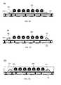
- Heat spreadersincluding drop-in heat spreaders, heat sinks, and heat pipes have been used in the past to enhance thermal performances of IC packages. Further descriptions of example heat spreaders are provided in U.S. Pat. No. 6,552,428, entitled “Semiconductor Package Having An Exposed Heat Spreader”, issued Apr. 22, 2003, which is incorporated by reference herein in its entirety. Further descriptions of example heat pipes are provided in Zhao and Avedisian, “Enhancing Forced Air Convection Heat Transfer From An Array Of Parallel Plate Fins Using A Heat Pipe, Int. J. Heat Mass Transfer, Vol. 40, No. 13, pp. 3135-3147 (1997).
- FIG. 1Ashows a die up plastic ball grid array (PBGA) package 100 integrated with a drop-in heat spreader 104 .
- PBGAdie up plastic ball grid array
- IC die 102is attached to a substrate 110 by die attach material 106 and is interconnected with wirebond 114 .
- Package 100can be connected to a printed wire board (PWB) (not shown) by solder balls 108 .
- PWBprinted wire board
- a drop-in heat spreader 104is mounted to substrate 110 , and conducts heat away from die 102 .
- Mold compound 112encapsulates package 100 , including die 102 , wirebond 114 , all or part of drop-in heat spreader 104 , and all or part of the upper surface of substrate 110 .
- Drop-in heat spreader 104is commonly made of copper or other material that is thermally more conductive than mold compound 112 . Thermal conductivity values are around 390 W/m*° C. for copper and 0.8 W/m*° C. for mold compound materials, respectively.
- Thermal enhancement methodssuch as shown in FIG. 1A rely on heat removal from the entire chip or from the entire package. They maintain semiconductor temperature below the limit of operation threshold by cooling the entire chip indiscriminately. These methods are often ineffective and inadequate to reduce the temperature of the hotspots relative to the rest of the chip, such that operation of the chip is still limited by the hotspots.
- FIG. 1Bshows a perspective view of a silicon die 102 , and in particular shows the temperature distribution on silicon die 102 in a PBGA with no external heat sink.
- the temperature difference across the die 102is 13.5° C.
- FIG. 1Cshows die 102 of FIG. 1B , illustrating the effect of adding a drop in heat spreader and a heat sink to the package of die 102 .
- the temperature differenceremains 13.0° C. with a large size (45 mm ⁇ 45 mm ⁇ 25 mm) external aluminum pin-fin heat sink attached on top of the exposed drop-in heat spreader. Both the drop-in heat spreader and the external heat sink are ineffective to reduce the on-chip temperature differences caused by the hot spots.
- thermoelectric coolerTEC
- FIG. 135-143A further description regarding on-chip cooling with TECs is provided in Snyder et al, “Hot Spot Cooling using Embedded Thermoelectric Coolers,” 22nd IEEE SEMI-THERM, Symposium, pp. 135-143 (2006), which is incorporated by reference herein in its entirety.
- an IC device packageincludes an IC die having a contact pad, where the contact pad is located on a hotspot on a surface of the IC die.
- a thermal interconnect memberis attached to the hot spot.
- the packageis encapsulated in a mold compound.
- the die and thermal interconnect memberare also electrically coupled.
- the packagealso includes a heat spreader.
- the heat spreadermay be thermally coupled to the thermal interconnect member.
- the heat spreaderis also electrically coupled to the thermal interconnect member.
- the heat spreaderis completely encapsulated in mold compound.
- the heat spreaderis at least partially exposed.
- the heat spreaderhas a plated area at a location corresponding to a location of the thermal interconnect member.
- an integrated circuit (IC) packageis manufactured by a method which includes attaching an IC die to a substrate, enabling electrical interconnection between the die and the substrate through a wire bonding process, coupling at least one thermal interconnect member to at least one contact pad on the die, and encapsulating the package in a mold compound or other encapsulating material.
- a portion of a thermal interconnect member(or a plurality of thermal interconnect members) is exposed.
- an entire layer of mold compoundis removed to expose the thermal interconnect member.
- a cavityis carved into the mold compound to expose the thermal interconnect member.
- the manufacturing methodfurther includes coupling a heat spreader to the exposed thermal interconnect member.
- the heat spreaderhas plating at one or more location corresponding to the thermal interconnect member.
- a dieis analyzed to determine a location of at least one hotspot on a surface of the die that results from operation of the die.
- the analysisincludes mapping functional blocks of the die to determine one or more hotspots.
- the analysisincludes performing a thermal analysis of the die during operation to locate one or more hotspots.
- a packagein another aspect of the invention, includes a substrate having opposing first and second surfaces, an IC die mounted to the first surface of the substrate, a heat spreader, and a thermal interconnect member that couples the first surface of the substrate to a surface of the heat spreader.
- FIG. 1Aillustrates a conventional IC package.
- FIGS. 1B and 1Cillustrate temperature distributions across a die in the conventional IC package of FIG. 1C using conventional cooling methods.
- FIGS. 2A-2Billustrate perspective views of example ball grid array (BGA) packages with cut away portions, according to exemplary embodiments of the invention.
- BGAball grid array
- FIG. 2Cillustrates a cross-sectional view of an example BGA package, according to an exemplary embodiment of the invention.
- FIG. 2Dillustrates a perspective view of an example ball grid array (BGA) package with a cut away portion, according to an exemplary embodiment of the invention.
- BGAball grid array
- FIG. 2Eillustrates a perspective view of an example ball grid array (BGA) package with a cut away portion, according to an exemplary embodiment of the invention.
- BGAball grid array
- FIG. 2Fillustrates a cross-sectional view of an example BGA package, according to an exemplary embodiment of the invention.
- FIGS. 3A-3Eillustrate cross-sectional views of example fine pitch ball grid array (BGA) packages having a heat spreader, according to exemplary embodiments of the invention.
- BGAball grid array
- FIGS. 4A-4Billustrate cross-sectional views of example plastic ball grid array (PBGA) packages having a heat spreader, according to exemplary embodiments of the invention.
- PBGAplastic ball grid array
- FIGS. 5A-5Cillustrate cross-sectional views of example leadframe packages having a heat spreader, according to exemplary embodiments of the invention.
- FIGS. 6A-6Billustrate example no-lead quad flat package (QFN) packages having a heat spreader, according to exemplary embodiments of the invention.
- FIG. 7Ashows a flowchart providing examples steps for assembling an integrated circuit package, according to exemplary embodiments of the invention.
- FIG. 7B-7Fillustrate cross-sectional views of an integrated circuit package during various phase of assembly, where encapsulation occurs before heat spreader attachment, according to exemplary embodiments of the invention.
- FIG. 8Ashows a flowchart providing examples steps for assembling an integrated circuit package, according to exemplary embodiments of the invention.
- FIG. 8B-8Cillustrate cross-sectional views of attaching a heat spreader to an integrated circuit package, according to exemplary embodiments of the invention.
- FIG. 9Ashows a flowchart providing examples steps for assembling an integrated circuit package, according to exemplary embodiments of the invention.
- FIG. 9B-9Dillustrate cross-sectional views of an integrated circuit package during various phase of assembly, where encapsulation occurs after heat spreader attachment, according to exemplary embodiments of the invention.
- FIG. 9Eshows a flowchart providing examples steps for assembling an integrated circuit package, according to exemplary embodiments of the invention.
- FIG. 9F-9Hillustrate cross-sectional views of an integrated circuit package during various phase of assembly, where encapsulation occurs after heat spreader attachment, according to exemplary embodiments of the invention.
- FIGS. 10A-10Cillustrate cross-sectional views of example BGA packages having a heat spreader thermally coupled to the package substrate, according to exemplary embodiments of the invention.
- Methods, systems, and apparatuses for IC device packaging technologyare described herein. In particular, methods, systems, and apparatuses for the (1) cooling of hotspots on IC semiconductor die, (2) heat spreading for IC packages, and (3) thermal interconnection technology in IC packaging are described.
- references in the specification to “one embodiment,” “an embodiment,” “an example embodiment,” etc.,indicate that the embodiment described may include a particular feature, structure, or characteristic, but every embodiment may not necessarily include the particular feature, structure, or characteristic. Moreover, such phrases are not necessarily referring to the same embodiment. Further, when a particular feature, structure, or characteristic is described in connection with an embodiment, it is submitted that it is within the knowledge of one skilled in the art to effect such feature, structure, or characteristic in connection with other embodiments whether or not explicitly described.
- Embodiments of the inventionprovide enhanced heat removal at desired locations on the surface of the semiconductor die.
- entire IC die and/or IC package surfacesare cooled to keep the peak temperatures on the IC die below an operation threshold limit.
- one or more thermal interconnect membersare coupled to one or more surfaces of an IC die.
- the thermal interconnect membersremove heat from hot spots on the die.
- the thermal interconnect membersprovide one or more paths for heat transfer from the IC die through a mold that encapsulates the die to the outside environment.
- the thermal interconnect membersare coupled to a heat spreader.
- the thermal interconnect membersWhen the thermal interconnect members are coupled to a heat spreader integrated in the package, the thermal interconnect members function as thermal bridges through the mold that fills a gap between the die and heat spreader. Locations for the positioning the thermal interconnect members in contact with the die may be selected, by using an on-chip power density map and/or based on chip layout, for example.
- one or more of the thermal interconnect membersmay be implemented with or without a heat spreader in all types of IC packages such as plastic ball grid array (PBGA), fine pitch ball grid array (BGA), land grid array (LGA), pin grid array (PGA), post-molded plastic leadframe packages such as quad flatpack (QFP) and no-lead quad flatpack (QFN) packages, and micro leadframe packages (MLP).
- IC packagessuch as plastic ball grid array (PBGA), fine pitch ball grid array (BGA), land grid array (LGA), pin grid array (PGA), post-molded plastic leadframe packages such as quad flatpack (QFP) and no-lead quad flatpack (QFN) packages, and micro leadframe packages (MLP).
- PBGAplastic ball grid array
- BGAfine pitch ball grid array
- LGAland grid array
- PGApin grid array
- post-molded plastic leadframe packagessuch as quad flatpack (QFP) and no-lead quad flatpack (QFN) packages
- MLPmicro leadframe packages
- embodimentsmay be
- thermal interconnect membersare thermally conductive solder balls, solder bumps, posts, or other thermally conductive structures.
- the thermal interconnect membersare also electrically conductive.
- exemplary embodiments using a solder ball-based thermal interconnect structureare referred to below to explain the principles of the invention. However, embodiments may use other thermal interconnect structures.
- Thermal interconnect membersmay be made of a metal, such as gold, copper, aluminum, silver, nickel, or tin, may be made of a combination of metals/alloy, such as solder, a eutectic (tin, lead), a lead-free solder, may be made of a thermally conductive epoxy or other adhesive material, or may be made of other thermally conductive materials.
- a thermal interconnect memberis made of a core material that is coated with a bonding material such as solder, gold, silver, an epoxy, or other joining materials that mechanically bonds the thermal interconnect member with contact pads on a semiconductor die.
- thermal interconnect membersmay be pre-deposited at pre-defined contact pads on a surface of the semiconductor die.
- one or more thermal interconnect membersare also coupled to a heat spreader.
- thermal interconnect memberswith a high power dissipation density to contact pads at areas on the die, which may be referred to as points or “blocks”
- heat generated within these hotspotscan be conducted away from the IC die directly to the external environment or through a thermally conductive heat spreader (if present) to the environment.
- the placement of the one or more thermal interconnect membersis based on a power map of a semiconductor die for a specific application.
- the same semiconductor diemay have different on-chip thermal interconnect member locations if a different power maps results from the application. For example, this may occur when different functional blocks of the die switch from a “power-up” mode to a “power-down” mode, or vice versa, for different applications.
- a dieis analyzed to determine a location of at least one hotspot on a surface of the die that results from operation of the die.
- the analysisincludes mapping functional blocks of the die to determine one or more hotspots.
- the analysisincludes performing a thermal analysis/measurement (e.g., as shown in FIGS. 1B and 1C ) of the die during operation to locate one or more hotspots.
- a thermal analysis/measuremente.g., as shown in FIGS. 1B and 1C
- one or more hotspotsmay be determined that are located on a surface of the die among other locations of the die that are relatively less hot (cooler) than the hotspots, and thus may need relatively less heat spreading than the hotspots.
- the one or more determined hotspotshave corresponding thermal interconnect members specifically targeted to them (mechanically/thermally coupled to them), to conduct heat from the hotspots, while conducting less heat from the cooler spots/areas (because a thermal interconnect has not been directly applied to the cooler spots/areas).
- a thermal signature of the die surfacecan be made more uniform (cooling the hotspots to be closer in temperature to the cooler spots/areas).
- some dieshave peripheral bond pads (e.g., formed in one or more rings) at a surface of the die for internal I/O signals to be accessible externally from the die.
- First ends of wire bondsattach to the peripheral bond pads, and second ends of the wire bonds attach to the package substrate or other structures of the package.
- contact padsare attached to hotspots located in a central region of the surface of the die outside of the peripheral region of the wire bond pads, but in embodiments one or more contact pads may be located in a peripheral region of the surface of the die.
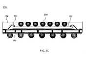
- FIGS. 2A-2Bshow perspective cut-away views of an exemplary embodiment of a die up BGA package 200 .
- FIG. 2Cillustrates a side cross sectional view of package 200 .
- an IC die 102is electrically connected by a plurality of wire bonds 114 to conductive features (e.g., traces, bond fingers, etc) such as a trace 210 on a top surface of a substrate 110 .
- the conductive features on the top surface of substrate 110are electrically coupled through substrate 110 (e.g., through one or more electrically and/or non-electrically conductive layers) to solder ball pads on a bottom surface of substrate 110 .
- Solder balls 108are coupled to the solder ball pads, and are configured to be coupled to a circuit board, such as a printed circuit board (PCB) or printed wire board (not shown in FIGS. 2A-2C ).
- PCBprinted circuit board
- a top surface of die 102has at least one contact pad 202 , to which at least one thermal interconnect member 208 is coupled.
- die 102can have any number of contact pads 202 , each for coupling with a thermal interconnect member 208 .
- Contact pads 202are located at pre-determined hotspots (not shown) on die 102 .
- Hotspots of die 102are locations on die 102 that are generally hotter than other locations on die 102 , although contact pads 202 may be located on locations of die 102 that are not necessarily hotter than other locations of die 102 .
- Mold compound 112encapsulates package 200 .
- thermal interconnect members 208are completely covered with mold compound 112 .
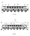
- FIGS. 2D-2Eshow perspective views of an exemplary embodiment of a die up BGA IC package 250 .
- FIG. 2Fillustrates a side cross sectional view of package 250 .
- Package 250is similar to package 200 , except that mold compound 112 does not encapsulate top surfaces 252 of thermal interconnect members 208 .
- a top layer of mold compound 112is removed to expose surfaces 252 of thermal interconnect members 208 .
- thermal interconnect members 208are truncated to form the planar exposed surfaces 252 of thermal interconnect members 208 , and surfaces 252 are co-planar with a top surface of mold compound 112 .
- Surfaces 252can also be referred to as thermal contact pads.
- Exposed surfaces 252 on package 250can be used for electrical connections (e.g., ground, power, or signal) to die 102 .
- electrical connectionse.g., ground, power, or signal
- a heat spreaderis not present.
- thermal performancemay be less than if heat spreader is present (as described below).
- the improvement in thermal performance even without a heat spreadermay be significant in a particular application due to a reduced junction-to-case thermal resistance resulting from the displacement of mold compound 112 by thermal interconnect members 208 .
- thermal interconnect members 208are solder balls
- a junction-to-case thermal resistanceis reduced because the thermal conductivity of typical (lead-free and tin/lead) IC package solder balls is around 50 ⁇ 60 W/m*° C., which is many times higher than a typical mold compound 112 , which may have a thermal conductivity of approximately 0.8 W/m*° C., for example.
- the solder balls forming thermal interconnect members 208 attached to IC die 102extend the heat conduction area from the surface of die 102 to a top surface of mold compound 112 .
- the thermal performance improvementis particularly significant for packages with a small size of die 102 , when the solder balls displace a relatively large area of mold compound 112 on the top surface of die 102 , providing a conductive path for heat dissipation through the top surface of package 250 .
- an external heat sink devicesuch as a heat sink or a metal plate, is attached to the top of a package such as packages 200 and 250 , the thermal performance of the package may improve. Examples of such embodiments are described in detail below.
- thermal interconnectsfacilitate on-chip power/heat dissipation from pre-selected locations on a semiconductor die.
- at least one thermal interconnectis attached to an IC die and coupled to at least one heat spreader embedded or attached to the IC package.
- the heat spreaderis encapsulated in a mold compound. The heat spreader may be exposed on a top surface of the package for heat dissipation to the ambient environment, including for attachment of a heat sink. The heat spreader can alternatively be entirely encapsulated within the mold compound of a molded IC package.
- the heat spreadermay have any of a variety of shapes and may include holes, slots, or other surface features for mold locking, heat dissipation, stress reduction, and/or improved reliability.
- the heat spreadermay be made of metal such as copper, copper alloys, other materials typically used in leadframe packages (C151, C194, EFTEC-64T, C7025, etc.), aluminum, other metals or combinations of metals/alloy, and/or thermally conductive nonmetallic materials.
- the heat spreadermay be a flexible tape substrate such as a polyimide tape substrate with one or more metal foil layers laminated on polyimide film.
- the heat spreadermay be made of a thermally conductive but electrically non-conductive material, such as a thermally conductive ceramic, or it may also be electrically conductive.
- a distance between a bottom surface of an integrated heat spreader and a top surface of the dieis less than a “loop-height” of the wire bond (i.e., a distance from the apex of the wire loop to the surface of IC die).
- a size of the heat spreadermay be confined by a space between the wire bond pads on the opposite sides of the top surface of the IC die.
- the distance between the bottom of the heat spreader and the top of dieis greater than the loop-height of wire bond.
- the size of the heat spreaderis not limited by the distance between the bond pads on the opposite sides of the surface of the die.
- the size of the heat spreadermay be greater than the size of the die, even if all four edges of surface of the die have wire bond interconnections.
- a larger heat spreadermay deliver increased hotspot cooling due to a larger area for heat dissipation.
- a pedestalmay be used that has an area less than an area of the die, and that extends towards the top surface of the IC die.
- thermal interconnectsmay be attached to the bottom of the heat spreader that can be thermally coupled with a corresponding thermal interconnect attached to the IC die.
- an integrated heat spreaderis completely encapsulated by mold compound. In another embodiment, it is partially exposed through the mold top, such as in manner similar to drop-in heat spreader 104 shown in FIG. 1A .
- one or more thermal interconnectsmay be attached to the ground or power net of the IC die to provide an alternative route for current or on-chip power delivery from the heat spreader. Examples of such an arrangement are described in U.S. patent application Ser. No. 10/952,172, titled “Die Down Ball Grid Array Packages And Method For Making Same,” filed Sep. 29, 2004, which is incorporated herein by reference in its entirety. This may be effective in reducing the lengths of on-chip power supply current paths, thus reducing IR voltage drops within the IC die.
- the size of the heat spreaderis less than a size of the package mold body, as illustrated in FIGS. 3A-3C .
- the size of the heat spreader sizecan also be substantially the same size as the package mold body, or larger than the size of package mold body. Examples of this are described in U.S. patent application Ser. No. 10/870,927, titled “Apparatus and Method for Thermal and Electromagnetic Interference (EMI) Shielding Enhancement in Die-Up Array Packages,” filed Jun. 21, 2004, which is incorporated by reference herein in its entirety.
- EMIThermal and Electromagnetic Interference
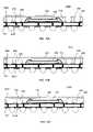
- FIGS. 3A-3Eillustrate exemplary embodiments of molded plastic fine pitch ball grid array (BGA) packages having a heat spreader 302 which is at least partially covered by mold compound 112 .
- BGAball grid array
- the configuration of heat spreader 302is varied from package to package.
- FIG. 3Aillustrates a package 300 having a planar heat spreader 302 integrated with package 300 in a partially embedded manner, having a planar top surface 304 of heat spreader 302 exposed (not covered by mold compound 112 ).
- IC die 102is electrically interconnected to substrate 110 by one or more wire bonds 114 .
- One or more thermal interconnect members 208are attached to the top surface of die 102 .
- Mold compound 112encapsulates die 102 , wire bonds 114 , a top surface of substrate 110 , and thermal interconnect members 208 .
- mold compound 112can be formed on substrate 110 using a mold process, a saw singulation technique, or other forming technique.
- a planar bottom surface 306 of heat spreader 302is coupled to a top portion of each of thermal interconnect members 208 .
- heat spreader 302is partially encapsulated by mold compound 112 .
- Bottom surface 306 and the perimeter edges of heat spreader 302are in contact with mold compound 112 , while the top surface 304 of heat spreader 302 is not covered by mold compound.
- Top surface 304 of heat spreader 302is co-planar with a top surface of mold compound 112 .
- heat spreader 302may be partially or completely encapsulated by mold compound 112 . Furthermore, although shown as planar in FIG. 3A , in other embodiments, heat spreader 302 may have other shapes, including regular or irregular shape and planar or non-planar.
- FIG. 3Billustrates a package 350 similar to package 300 , but having a non-planar heat spreader 302 integrated with package 300 in a partially embedded manner.
- heat spreader 302has cap-like shape, with a cavity side of heat spreader 302 facing towards die 102 .
- Bottom surface 306 of heat spreader 302is coupled to a top portion of each of thermal interconnect members 208 .
- a planar portion 308 of top surface 304 of heat spreader 302is not covered by mold compound 112 , while the remainder of heat spreader 302 is covered by mold compound 112 .
- a perimeter angled wall portion 310 of heat spreader 302that angles outward as it extends from the remaining planar portion of heat spreader 302 is covered by mold compound 112 .
- FIG. 3Cillustrates a package 360 having a planar heat spreader 302 (similar to FIG. 3A ) integrated with package 360 in a non-embedded configuration.
- Bottom surface 306 of heat spreader 302is coupled to a top portion of each of thermal interconnect members 208 .
- Heat spreader 302is attached to a planar top surface of mold compound 112 .
- bottom surface 306 of heat spreader 302is in contact with mold compound 112 , while the remainder of heat spreader 302 is not in contact with mold compound 112 .
- heat spreader 302can be attached to package 360 after mold compound 112 is applied.
- FIG. 3Dillustrates a package 370 similar to package 360 , but having a non-planar heat spreader 302 .
- Heat spreader 302has a planar central portion 312 connected to a surrounding plurality of leads 314 that are configured to couple heat spreader 302 to a circuit board (not shown in FIG. 3D ) when package 370 is mounted thereto.
- Bottom surface 306 of central portion 312attaches thermal interconnect members 208 .
- Leads 314 of heat spreader 302each bend down from central portion 312 at a shoulder toward the circuit board.
- An end of each lead 314may have a foot 372 that bends outward from heat spreader 302 , and is configured to mount to a circuit board, such as for direct thermal and/or electrical coupling to the circuit board.
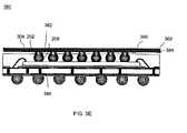
- FIG. 3Eillustrates a package 380 , where thermal interconnect members 208 are truncated solder balls having exposed surfaces 252 , similar to the configuration of FIG. 2F .
- heat spreader 302has pads 382 located at locations corresponding to surfaces 252 of thermal interconnect members 208 .
- Pads 382are pre-deposited with a material 386 prior to attachment to surfaces 252 .
- Pre-deposited pads 382may be plated with a thermally conductive material 386 , such as a solder or epoxy that mechanically attaches heat spreader 302 to thermal interconnect members 208 .
- plating material 386is also electrically conductive.
- Heat spreader 302is coupled to the thermal interconnect members 208 during a reflow, curing, or other attachment process. Furthermore, in an embodiment, an air gap 384 may optionally exist under heat spreader 302 , between bottom surface 306 of heat spreader 302 and a top surface of mold compound 112 , after manufacture is complete. Plating material 386 supports heat spreader 302 above mold compound 112 at a distance to provide air gap 384 .
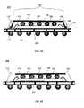
- FIGS. 4A-4Billustrate exemplary embodiments of molded plastic ball grid array (PBGA) packages having at least one thermal interconnect member 208 coupled to an integrated heat spreader 302 .
- PBGAmolded plastic ball grid array
- FIG. 4Ashows a package 400 , with a partially embedded heat spreader 302 , according to an example embodiment of the present invention.
- IC die 102is electrically interconnected to substrate 110 by wire bonds 114 .
- One or more thermal interconnect members 208are coupled between die 102 and heat spreader 302 .
- thermal interconnect members 208are shown having a truncated top portion, similar to as described above with respect to FIG. 2F .
- Bottom surface 306 of heat spreader 302attaches to top surfaces 252 of thermal interconnect members 208 .
- Mold compound 112is formed by a molding process, and encapsulates much of package 400 , including die 102 , wire bond 114 , a portion of the top surface of substrate 110 , and all of heat spreader 302 except for a planar top portion 402 of heat spreader 302 .
- heat spreader 302is cap-shaped, having a cavity 474 facing towards die 102 , and enclosing thermal interconnect members 208 , die 102 , and wire bonds 114 on the top surface of substrate 110 .
- the cap shape of heat spreader 302has an top planar portion, outward slanting side walls that extend downward from the top planar portion and that surround cavity 474 , and a perimeter rim portion 404 around a bottom edge of the side walls.
- a bottom surface of perimeter rim portion 404 of heat spreader 302is attached to the top surface of substrate 110 by an adhesive material 406 , such as an epoxy, adhesive, solder, or other adhesive.
- Heat spreader 302may be any regular or irregular shape, and planar or non-planar.
- FIG. 4Bshows a package 450 similar to package 400 of FIG. 4A , except that heat spreader 302 is planar in shape.
- Top surface 304 of heat spreader 302is not covered by mold compound 112 .
- the outer edges of heat spreader 302are covered by mold compound 112 .
- Bottom surface 306 of heat spreader 302is embedded in mold compound 112 , and attaches to top surfaces 252 of thermal interconnect members 208 .
- FIGS. 5A-5Cillustrate example embodiments having at least one thermal interconnect member 208 and a heat spreader 502 integrated with a leadframe package.
- FIG. 5Aillustrates a package 500 in which die 102 is attached to a die attach pad 504 of a leadframe 516 .
- Leadframe 516includes a plurality of leads 518 and die attach pad 504 .
- Die 102is electrically interconnected with die attach pad 504 and/or leads 518 by one or more wire bonds 514 .
- leads 518may be electrically interconnected with die attach pad 504 with one or more wire bonds 514 .
- Heat spreader 502is cap-shaped, having a cavity 520 facing towards die 102 .
- Die 102 and a bottom surface 522 in cavity 520 of heat spreader 502are connected by one or more thermal interconnect members 208 , which may or may not be truncated.
- Package 500is encapsulated by mold compound 512 , which fills a gap between heat spreader 502 and die 102 , including cavity 520 .
- a bottom surface of a perimeter rim portion 524 of heat spreader 502is mounted to lead frame 516 . As shown in FIG. 5A , the bottom surface of perimeter rim portion 524 and lead frame 516 may be configured to interlock for improved mechanical coupling.
- FIG. 5Billustrates a package 550 similar to package 500 of FIG. 5A , except that heat spreader 502 is planar, and thus is not mounted to lead frame 516 .
- FIG. 5Cillustrates a package 560 similar to package 550 of FIG. 5B , except that heat spreader 502 is completely embedded in mold compound 112 .
- die-up configurationsi.e., circuit side of die 102 is facing away from the circuit board when mounted thereto
- FIG. 5A-5Cthese are shown for the purpose of illustration.
- Embodiments of the present inventionare also applicable to die-down leadframe packages.
- one or more thermal interconnect members 208may be used in a leadframe package without an integrated heat spreader, in a similar manner as shown in FIG. 2A-2F for BGA packages.
- FIGS. 6A and 6Billustrate example embodiments of no-lead quad flat packages (QFP), also known as micro leadframe packages (MLP) or micro lead frame (MLF) IC packages, each having at least one thermal interconnect member 208 and a heat spreader 602 integrated therein.
- QFPno-lead quad flat packages
- MLPmicro leadframe packages
- MMFmicro lead frame
- FIG. 6Aillustrates a package 600 in which die 102 is attached to a die attach pad 604 .
- Die 102is electrically interconnected with die attach pad 604 and/or leads 616 by one or more wire bonds 614 .
- Heat spreader 602is cap-shaped, having a cavity 620 facing towards die 102 .
- Die 102 and a bottom surface 622 in cavity 620 of heat spreader 602are connected by one or more thermal interconnect members 208 , which may or may not be truncated.
- Package 600is encapsulated by mold compound 612 , which fills a gap between heat spreader 602 and die 102 , including cavity 620 .
- a bottom surface of a perimeter rim portion 624 of heat spreader 602is mounted to leads 616 . As shown in FIG. 6A , the bottom surface of perimeter rim portion 624 and leads 616 may be configured to interlock for improved mechanical coupling.
- FIG. 6Billustrates a package 650 similar to package 600 of FIG. 6A , except that heat spreader 602 is planar, and thus is not mounted to leads 616 .
- FIG. 7Ashows a flowchart 700 providing an example process for manufacturing embodiments of the invention.
- Flowchart 700is described with reference to FIGS. 7B-D , which show a BGA package at various stages of manufacture.
- Flowchart 700may be applied in a modified or non-modified manner to manufacture other package types, as would be understood by persons skilled in the relevant art(s) from the teachings herein.
- an optional step of attaching a heat spreader(step 710 ) may be performed depending on whether a heat spreader is desired to be present.
- Flowchart 700begins with step 701 .
- a dieis mounted to a substrate.
- the dieis die 102 shown in FIGS. 2A-2C , which is attached to substrate 110 using die attach material 106 .
- Die attach material 106may be any type of suitable adhesive material, such as an epoxy and/or film adhesive, or other type of adhesive material or attachment mechanism.
- thermal interconnectsare mounted on a top surface of the die.
- one or more thermal interconnect members 208are mounted on contact pads 202 on die 102 , as shown in FIGS. 2A-2C .
- FIG. 7Billustrates an example partially assembled package 750 after steps 701 and 702 .
- a conventional ball mount process used for mounting solder balls to the bottom of BGA packagesmay be used to mount a solder ball to die 102 , when thermal interconnect members 208 are solder balls.
- step 704wire bonds are coupled between the die and substrate.
- die 102may be electrically connected to substrate 110 through a wire bonding process that attaches wire bonds 114 .
- FIG. 7Cillustrates an example partially assembled package 760 after steps 701 - 704 .
- the packageis encapsulated in mold compound.
- the mold compoundis mold compound 112 .
- mold compound 112covers die 102 , wire bond 114 , at least one thermal interconnect member 208 , and all or part of substrate 110 .
- FIG. 7Dillustrates an example a partially assembled package 770 after steps 701 - 706 .
- a portion or all of a top layer of the mold compoundis removed.
- a layer of mold compound 112is removed such that one or more thermal interconnect members 208 are truncated (i.e., a top portion of thermal interconnect member 208 is removed along with a portion of the top layer, or the entire top layer of mold compound 112 ).
- FIG. 7Ashows step 708 as optionally including one of steps 708 a and 708 b .
- step 708 aan entire top layer of the mold compound is removed, such as shown in FIG. 2F .
- FIG. 7Eillustrates an example implementation of step 708 a , where a grinding tool 702 is used to grind away an entire top layer of molding compound 112 , thereby grinding away a portion of thermal interconnect members 208 and exposing surface 252 of thermal interconnect members 208 .
- a cavityis formed in the mold compound.
- FIG. 7Fillustrates an example implementation of step 708 b .
- a routing tool 704is used to route away a central portion of a top layer of mold compound 112 to form a cavity 706 in the top layer of mold compound 112 .
- routing tool 704routes away a portion of thermal interconnect members 208 that are under cavity 706 , to expose surface 252 of the centrally located thermal interconnect members 208 .
- steps 708 , 708 a , and 708 bmay be used in steps 708 , 708 a , and 708 b to remove mold top material and expose and/or truncate one or more thermal interconnects.
- Other surface machining methodssuch as etching or laser machining may used to remove mold material and expose thermal/electrical interconnect elements.
- step 708(and sub-steps 708 a and 708 b ) is optional.
- step 708is not performed, and a layer and/or cavity of mold compound is not removed.
- a heat spreaderis attached to the package.
- the heat spreaderis heat spreader 302 , 502 , 602 , or 702 , described above.
- optional step 710is not performed.
- the heat spreaderis coupled to the one or more exposed thermal interconnects, which may or may not be truncated.
- step 704may be performed before thermal interconnects are attached to the die surface in step 702 .
- FIG. 8Aillustrates a flowchart 800 showing a process for attaching a heat spreader to an IC package.
- Flowchart 800is described with reference to FIGS. 8B-C , which show a BGA package at various stages of manufacture.
- Flowchart 800may be applied in a modified or non-modified manner to manufacture other package types, as would be understood by persons skilled in the relevant art(s) from the teachings herein
- Flowchart 800begins in step 802 .
- a heat spreader having one or more pre-plated padsis received.
- the heat spreaderis heat spreader 302 , as shown in FIG. 8B .
- FIG. 8Bshows a partially assembled package 850 and heat spreader 302 .
- Heat spreader 302has pads 382 that are plated with plating material 386 .
- Plating material 386may be a thermally conductive substance, for example, solder or epoxy.
- step 804the heat spreader is placed on the package.
- heat spreader 302is placed on partially assembled package 860 , such that plating material 386 is in contact with surface 252 of thermal interconnects 252 .
- the heat spreaderis caused to become attached to the package.
- a reflow or curing processmay be conducted.
- the reflow or curing processcauses heat spreader 302 to become attached to partially assembled package 860 , to form package 870 , as illustrated in FIG. 8C .
- a reflow processmay be used for a solder plating embodiment for plating material 386 , or a curing process may be used for an epoxy material embodiment of plating material 386 .
- the completed packagemay have an air gap 384 between heat spreader 302 and mold compound 112 .
- FIG. 9Ashows a flowchart 900 providing an example process for manufacturing embodiments of the invention.
- Flowchart 900is described with reference to FIGS. 9B-D , which show a BGA package at various stages of manufacture.
- Flowchart 900may be applied in a modified or non-modified manner to manufacture other package types, as would be understood by persons skilled in the relevant art(s) from the teachings herein.
- Flowchart 900begins with step 902 .
- a dieis mounted to a substrate.
- the dieis die 102 of FIG. 3A , which is attached to substrate 110 .
- step 904wire bonds are coupled between the die and the substrate.
- die 102is electrically connected to substrate 110 through a wire bonding process that applies wire bonds 114 .
- thermal interconnectsare mounted to a top surface of the die.
- one or more thermal interconnect members 208may be mounted to contact pads 202 on the top surface of die 102 .
- FIG. 9Billustrates an example partially assembled package 920 after steps 902 , 904 , and 906 .
- a conventional ball mount processused for mounting solder balls to the bottom of BGA packages is used to mount a thermal interconnect members 208 to die 102 .
- the heat spreaderis attached to the thermal interconnects.
- heat spreader 302is attached to thermal interconnect members 208 .
- heat spreader 302may have pre-plated pads, such as shown in FIG. 3E .
- FIG. 9Cillustrates an example partially assembled package 930 after steps 902 - 908 .
- step 910the package is encapsulated in mold compound.
- mold compound 112covers die 102 , wire bond 114 , at least one thermal interconnect member 208 , and all or part of substrate 110 .
- FIG. 9Dillustrates an example partially assembled package 940 after steps 902 - 910 .
- step 906may be performed before step 904 .
- thermal interconnectsmay be attached to the heat spreader before being attached to the die.
- FIG. 9Eshows a flowchart 950 providing an example process for manufacturing embodiments of the invention. Flowchart 950 is described with reference to FIGS. 9F-H , which show a BGA package at various stages of manufacture. Flowchart 950 may be applied in a modified or non-modified manner to manufacture other package types, as would be understood by persons skilled in the relevant art(s) from the teachings herein.
- Flowchart 950begins with step 952 .
- a dieis mounted to a substrate.
- the dieis die 102 of FIG. 3A , which is attached to substrate 110 .
- step 954wire bonds are coupled between the die and the substrate.
- die 102is electrically connected to substrate 110 through a wire bonding process that applies wire bonds 114 .
- thermal interconnectsare mounted to a bottom surface of the heat spreader.
- one or more thermal interconnect members 208may be mounted to bottom surface 306 of heat spreader 302 , as shown in FIG. 9F .
- a conventional ball mount processused for mounting solder balls to the bottom of BGA packages is used to mount thermal interconnect members 208 to heat spreader 302 .
- heat spreader 302has pre-plated pads (not shown in FIG. 9F ).
- step 958the thermal interconnects are attached to the top surface of the die.
- thermal interconnect members 208are attached to die 102 .
- FIG. 9Gillustrates an example partially assembled package 980 after step 958 .
- step 960the package is encapsulated in mold compound.
- mold compound 112is used to cover die 102 , wire bonds 114 , thermal interconnect members 208 , and all or part of substrate 110 .
- FIG. 9Hillustrates an example partially assembled package 990 after completion of steps 902 - 910 .
- thermal interconnect membersmay be used to couple a heat spreader to a substrate in an integrated circuit package.
- FIGS. 10A-10Cillustrate cross-sectional views of example BGA packages having a heat spreader thermally coupled to the package substrate, according to exemplary embodiments of the invention. The embodiments of FIGS. 10A-10C are provided for illustrative purposes.
- thermal interconnect membersmay be used in other types of IC packages to couple heat spreaders to substrates.
- the thermal interconnect memberswhen they are solder balls, they may be truncated or non-truncated.
- Other materialssuch as copper, gold, other metals and/or metal alloys can be used for thermal interconnect members, including the materials described elsewhere herein or otherwise known.
- FIGS. 10A-10Care generally similar to package 300 of FIG. 3A , with some differences described as follows.
- FIG. 10Ashows a package 1000 having a plurality of thermal interconnect members 208 that couple bottom surface 306 of heat spreader 302 to a top surface 1002 of substrate 110 .
- thermal interconnect members 208provided a thermally conductive path between substrate 110 and heat spreader 302 , such that heat generated by die 102 that passes into substrate 110 can be transferred to heat spreader 302 .
- Thermal interconnect member 208may be coupled to top surface 1002 of substrate 110 at a non-electrically conductive location of substrate 110 and/or an electrically conductive location of substrate 110 .
- a bottom surface of thermal interconnect member 208may be attached to a surface of a solder resist layer or dielectric layer of substrate 110 , which are typically non-electrically conductive, and have a relatively low degree of thermal conductivity.
- thermal interconnect member 208may be attached to an electrically conductive feature 1004 of substrate 110 , such as a trace, bond finger, contact pad, ground/power ring, etc., which are typically made of a metal (e.g., a metal foil, plating, etc) such as copper, aluminum, gold, tin, nickel, silver, another metal, or combination of metals/alloy.
- a metale.g., a metal foil, plating, etc
- thermal interconnect member 208may provide an electrically conductive path to heat spreader 302 when thermal interconnect member 208 is electrically conductive.
- heat spreader 302has an area that is smaller than an area of a top surface of mold compound 112 , such that a peripheral area of the top surface of mold compound 112 is not covered by heat spreader 302 .
- FIG. 10Bshows a package 1010 similar to package 1000 of FIG. 10A , except that heat spreader 302 has an area substantially the same as an area of the top surface of mold compound 112 .
- thermal interconnect members 208may be present in embodiments to couple heat spreader 302 to substrate 110 , including an array of thermal interconnect members 208 .
- a pair of rings of thermal interconnect members 208encircle die 102 on top surface 1002 of substrate 110 .
- Any number of such rings of thermal interconnect members 208may be present, when desired.
- FIG. 10Cshows a package 1020 similar to package 1010 of FIG. 10B , except that a single ring of thermal interconnect members 208 encircle die 102 on top surface 1002 of substrate 110 .
- flowcharts 700 , 900 , and 950can be modified to include a step of forming/attaching thermal interconnects to a heat spreader and/or to a substrate to be used to couple the heat spreader to the substrate.
- FIGS. 10A-10Cshow thermal interconnect members 208 coupled between substrate 110 and heat spreader 302
- packages 1000 , 1010 , 1020may also include thermal interconnect members 208 coupling the top surface of die 102 to heat spreader 302 .
Landscapes
- Engineering & Computer Science (AREA)
- Computer Hardware Design (AREA)
- Microelectronics & Electronic Packaging (AREA)
- Power Engineering (AREA)
- Physics & Mathematics (AREA)
- Condensed Matter Physics & Semiconductors (AREA)
- General Physics & Mathematics (AREA)
- Manufacturing & Machinery (AREA)
- Chemical & Material Sciences (AREA)
- Materials Engineering (AREA)
- Cooling Or The Like Of Semiconductors Or Solid State Devices (AREA)
Abstract
Description
- This application claims the benefit of U.S. Provisional Appl. No. 60/814,876, filed Jun. 20, 2006, which is herein incorporated by reference in its entirety.
- 1. Field of the Invention
- The invention relates generally to the field of integrated circuit (IC) device packaging technology, and more particularly to the cooling of hotspots on IC semiconductor die, heat spreading for IC packages, and thermal interconnection technology in IC packaging.
- 2. Background Art
- Electronic signals are carried by electrical current through conductors and transistors in a large scale integrated circuit (IC) fabricated on semiconductor substrate. The energy carried by the electrical current is partially dissipated along the paths of current flow through the IC in the form of heat. Heat generation in electronic semiconductor ICs is also known as power consumption, power dissipation, or heat dissipation. The heat generated, P, in an IC is the sum of dynamic power, PD, and static power, PS:
P═PD+PS=ACV2f+VIleak- where A is the gate activity factor, C is the total capacitance load of all gates, V is the peak-to-peak supply voltage swing, f is the frequency, and Ileakis the leakage current. The static power term, PS=VIleak, is the static power dissipated due to leakage current, Ileak. A further description regarding static power is provided in Kim et al, Leakage Current: Moore's Law Meets Static Power, IEEE Computer, 36(12): 68-75, December 2003, which is incorporated by reference herein in its entirety.
- The dynamic power term, PD=ACV2f, is the dynamic power dissipated from charging and discharging the IC device capacitive loads. Dynamic power consumption is thus proportional to the operating frequency and the square of operating voltage. Static power consumption is proportional to the operating voltage. Advances in transistor gate size reduction in semiconductor IC technology have reduced the operating voltage and power dissipation for single transistors. However, on-chip power densities are expected continue to rise in future technologies as the industry continues to follow the trend set forth by Moore's Law. In 1965, Intel co-founder Gordon Moore predicted that the number of transistors on a chip doubles about every two years. In addition to the increased number of transistors on a chip, the operating frequencies also double about every two years according to the 2004 International Technology Roadmap for Semiconductors (ITRS Roadmap) (http://www.itrs.net/Common/2004Update/2004—00_Overview.pdf). Because of the increased difficulties in controlling noise margins as voltage decreases, operating voltages can no longer be reduced as quickly as in the past for 130 nm gate lengths and smaller. Consequently, on-chip power dissipation will continue to rise. See Table 6 of the ITRS Roadmap. With the increased use of 65 nm technology in foundry processes and the commercialization of 45 nm technology, power consumption is now a major technical problem facing the semiconductor industry.
- Another characteristic of IC chips is the uneven distribution of temperature on a semiconductor die. More and more functional blocks are integrated in a single chip in system-on-chip (SOC) designs. Higher power density blocks create an uneven temperature distribution and lead to “hotspots,” also known as “hot blocks,” on the chip. Hotspots can lead to a temperature difference of about 5° C. to roughly 30° C. across a chip. Further description of hotspots is provided in Shakouri and Zhang, “On-Chip Solid-State Cooling For Integrated Circuits Using Thin-Film Microrefrigerators,” IEEE Transactions on Components and Packaging Technologies, Vol. 28, No. 1, March, 2005, pp. 65-69, which is incorporated by reference herein in its entirety.
- Since carrier mobility is inversely proportional to temperature, the clock speed typically must be designed for the hottest spot on the chip. Consequently, thermal design is driven by the temperature of these on-chip hotspots. Also, if uniform carrier mobility is not achieved across the IC die due to on-chip temperature variations across the die, this may result in variations in signal speed and in complicating circuit timing control.
- Heat spreaders, including drop-in heat spreaders, heat sinks, and heat pipes have been used in the past to enhance thermal performances of IC packages. Further descriptions of example heat spreaders are provided in U.S. Pat. No. 6,552,428, entitled “Semiconductor Package Having An Exposed Heat Spreader”, issued Apr. 22, 2003, which is incorporated by reference herein in its entirety. Further descriptions of example heat pipes are provided in Zhao and Avedisian, “Enhancing Forced Air Convection Heat Transfer From An Array Of Parallel Plate Fins Using A Heat Pipe, Int. J. Heat Mass Transfer, Vol. 40, No. 13, pp. 3135-3147 (1997).
- For example,
FIG. 1A shows a die up plastic ball grid array (PBGA)package 100 integrated with a drop-inheat spreader 104. Inpackage 100, IC die102 is attached to asubstrate 110 by dieattach material 106 and is interconnected withwirebond 114.Package 100 can be connected to a printed wire board (PWB) (not shown) bysolder balls 108. A drop-inheat spreader 104 is mounted tosubstrate 110, and conducts heat away from die102. Moldcompound 112 encapsulatespackage 100, including die102,wirebond 114, all or part of drop-inheat spreader 104, and all or part of the upper surface ofsubstrate 110. Drop-inheat spreader 104 is commonly made of copper or other material that is thermally more conductive thanmold compound 112. Thermal conductivity values are around 390 W/m*° C. for copper and 0.8 W/m*° C. for mold compound materials, respectively. - Thermal enhancement methods, such as shown in
FIG. 1A , rely on heat removal from the entire chip or from the entire package. They maintain semiconductor temperature below the limit of operation threshold by cooling the entire chip indiscriminately. These methods are often ineffective and inadequate to reduce the temperature of the hotspots relative to the rest of the chip, such that operation of the chip is still limited by the hotspots. - For example,
FIG. 1B shows a perspective view of asilicon die 102, and in particular shows the temperature distribution onsilicon die 102 in a PBGA with no external heat sink. The temperature difference across the die102 is 13.5° C.FIG. 1C shows die102 ofFIG. 1B , illustrating the effect of adding a drop in heat spreader and a heat sink to the package of die102. The temperature difference remains 13.0° C. with a large size (45 mm×45 mm×25 mm) external aluminum pin-fin heat sink attached on top of the exposed drop-in heat spreader. Both the drop-in heat spreader and the external heat sink are ineffective to reduce the on-chip temperature differences caused by the hot spots. - Active on-chip cooling methods that use electrical energy to remove heat from the IC chip are known in the art. For example, some have suggested pumping liquid coolant through micro-channels engraved in silicon to circulate on the semiconductor die and carry away waste heat. A further description regarding liquid cooling is provided in Bush, “Fluid Cooling Plugs Direct onto CMOS,” Electronic News, Jul. 20, 2005, http://www.reed-electronics.com/electronicnews/article/CA626959?nid=2019 &rid=550846255), which is incorporated by reference herein in its entirety. See also Singer, “Chip Heat Removal with Microfluidic Backside Cooling,” Electronic News, Jul. 20, 2005, which is incorporated by reference herein in its entirety.
- Other active cooling methods have been developed in an attempt to provide active on-chip cooling using a thin-film thermoelectric cooler (TEC). A further description regarding on-chip cooling with TECs is provided in Snyder et al, “Hot Spot Cooling using Embedded Thermoelectric Coolers,” 22nd IEEE SEMI-THERM, Symposium, pp. 135-143 (2006), which is incorporated by reference herein in its entirety.
- These active cooling methods require exotic and expensive fluid circulation or micro-refrigeration systems and add to the total power consumption of the package that must be removed. A separate power supply must also be integrated into the IC package to drive the fluid pumping or the TEC systems. These can be costly and can decrease component reliability. Because these solutions are typically expensive, their use is limited in cost sensitive applications such as consumer electronic devices.
- These cooling methods as discussed above are inadequate and/or difficult and expensive to implement for commercial applications. What is needed is an inexpensive and reliable system and method of selective heat removal from hot blocks or hotspots on semiconductor dice.
- Methods and apparatuses for improved integrated circuit (IC) packages are described herein.
- In an aspect of the invention, an IC device package includes an IC die having a contact pad, where the contact pad is located on a hotspot on a surface of the IC die. A thermal interconnect member is attached to the hot spot. In an aspect of the invention, the package is encapsulated in a mold compound. In a further aspect of the invention, the die and thermal interconnect member are also electrically coupled.
- In an aspect of the invention, the package also includes a heat spreader. The heat spreader may be thermally coupled to the thermal interconnect member. In a further aspect, the heat spreader is also electrically coupled to the thermal interconnect member. In an aspect of the invention, the heat spreader is completely encapsulated in mold compound. In another aspect, the heat spreader is at least partially exposed. In an aspect of the invention, the heat spreader has a plated area at a location corresponding to a location of the thermal interconnect member.
- In an aspect of the invention, an integrated circuit (IC) package is manufactured by a method which includes attaching an IC die to a substrate, enabling electrical interconnection between the die and the substrate through a wire bonding process, coupling at least one thermal interconnect member to at least one contact pad on the die, and encapsulating the package in a mold compound or other encapsulating material. In another aspect of the invention, a portion of a thermal interconnect member (or a plurality of thermal interconnect members) is exposed. In an example aspect, an entire layer of mold compound is removed to expose the thermal interconnect member. In another example aspect, a cavity is carved into the mold compound to expose the thermal interconnect member.
- In an aspect of the invention, the manufacturing method further includes coupling a heat spreader to the exposed thermal interconnect member. In an aspect, the heat spreader has plating at one or more location corresponding to the thermal interconnect member.
- In another aspect of the invention, a die is analyzed to determine a location of at least one hotspot on a surface of the die that results from operation of the die. In an aspect, the analysis includes mapping functional blocks of the die to determine one or more hotspots. In another aspect, the analysis includes performing a thermal analysis of the die during operation to locate one or more hotspots.
- In another aspect of the invention, a package includes a substrate having opposing first and second surfaces, an IC die mounted to the first surface of the substrate, a heat spreader, and a thermal interconnect member that couples the first surface of the substrate to a surface of the heat spreader.
- These and other objects, advantages and features will become readily apparent in view of the following detailed description of the invention. Note that the Summary and Abstract sections may set forth one or more, but not all exemplary embodiments of the present invention as contemplated by the inventor(s).
- The accompanying drawings, which are incorporated herein and form a part of the specification, illustrate the present invention and, together with the description, further serve to explain the principles of the invention and to enable a person skilled in the pertinent art to make and use the invention.
FIG. 1A illustrates a conventional IC package.FIGS. 1B and 1C illustrate temperature distributions across a die in the conventional IC package ofFIG. 1C using conventional cooling methods.FIGS. 2A-2B illustrate perspective views of example ball grid array (BGA) packages with cut away portions, according to exemplary embodiments of the invention.FIG. 2C illustrates a cross-sectional view of an example BGA package, according to an exemplary embodiment of the invention.FIG. 2D illustrates a perspective view of an example ball grid array (BGA) package with a cut away portion, according to an exemplary embodiment of the invention.FIG. 2E illustrates a perspective view of an example ball grid array (BGA) package with a cut away portion, according to an exemplary embodiment of the invention.FIG. 2F illustrates a cross-sectional view of an example BGA package, according to an exemplary embodiment of the invention.FIGS. 3A-3E illustrate cross-sectional views of example fine pitch ball grid array (BGA) packages having a heat spreader, according to exemplary embodiments of the invention.FIGS. 4A-4B illustrate cross-sectional views of example plastic ball grid array (PBGA) packages having a heat spreader, according to exemplary embodiments of the invention.FIGS. 5A-5C illustrate cross-sectional views of example leadframe packages having a heat spreader, according to exemplary embodiments of the invention.FIGS. 6A-6B illustrate example no-lead quad flat package (QFN) packages having a heat spreader, according to exemplary embodiments of the invention.FIG. 7A shows a flowchart providing examples steps for assembling an integrated circuit package, according to exemplary embodiments of the invention.FIG. 7B-7F illustrate cross-sectional views of an integrated circuit package during various phase of assembly, where encapsulation occurs before heat spreader attachment, according to exemplary embodiments of the invention.FIG. 8A shows a flowchart providing examples steps for assembling an integrated circuit package, according to exemplary embodiments of the invention.FIG. 8B-8C illustrate cross-sectional views of attaching a heat spreader to an integrated circuit package, according to exemplary embodiments of the invention.FIG. 9A shows a flowchart providing examples steps for assembling an integrated circuit package, according to exemplary embodiments of the invention.FIG. 9B-9D illustrate cross-sectional views of an integrated circuit package during various phase of assembly, where encapsulation occurs after heat spreader attachment, according to exemplary embodiments of the invention.FIG. 9E shows a flowchart providing examples steps for assembling an integrated circuit package, according to exemplary embodiments of the invention.FIG. 9F-9H illustrate cross-sectional views of an integrated circuit package during various phase of assembly, where encapsulation occurs after heat spreader attachment, according to exemplary embodiments of the invention.FIGS. 10A-10C illustrate cross-sectional views of example BGA packages having a heat spreader thermally coupled to the package substrate, according to exemplary embodiments of the invention.- Embodiments of the present invention will now be described with reference to the accompanying drawings. In the drawings, like reference numbers indicate identical or functionally similar elements. Additionally, the left-most digit(s) of a reference number identifies the drawing in which the reference number first appears.
- Methods, systems, and apparatuses for IC device packaging technology are described herein. In particular, methods, systems, and apparatuses for the (1) cooling of hotspots on IC semiconductor die, (2) heat spreading for IC packages, and (3) thermal interconnection technology in IC packaging are described.
- References in the specification to “one embodiment,” “an embodiment,” “an example embodiment,” etc., indicate that the embodiment described may include a particular feature, structure, or characteristic, but every embodiment may not necessarily include the particular feature, structure, or characteristic. Moreover, such phrases are not necessarily referring to the same embodiment. Further, when a particular feature, structure, or characteristic is described in connection with an embodiment, it is submitted that it is within the knowledge of one skilled in the art to effect such feature, structure, or characteristic in connection with other embodiments whether or not explicitly described.
- The present specification discloses one or more embodiments that incorporate the features of the invention. The disclosed embodiment(s) merely exemplify the invention. The scope of the invention is not limited to the disclosed embodiment(s). The invention is defined by the claims appended hereto.
- Furthermore, it should be understood that spatial descriptions (e.g., “above”, “below”, “left,” “right,” “up”, “down”, “top”, “bottom”, etc.) used herein are for purposes of illustration only, and that practical implementations of the structures described herein can be spatially arranged in any orientation or manner.
- Embodiments of the invention provide enhanced heat removal at desired locations on the surface of the semiconductor die. In conventional devices, entire IC die and/or IC package surfaces are cooled to keep the peak temperatures on the IC die below an operation threshold limit. In contrast, in an embodiment, one or more thermal interconnect members are coupled to one or more surfaces of an IC die. The thermal interconnect members remove heat from hot spots on the die. The thermal interconnect members provide one or more paths for heat transfer from the IC die through a mold that encapsulates the die to the outside environment.
- In a further embodiment, the thermal interconnect members are coupled to a heat spreader. When the thermal interconnect members are coupled to a heat spreader integrated in the package, the thermal interconnect members function as thermal bridges through the mold that fills a gap between the die and heat spreader. Locations for the positioning the thermal interconnect members in contact with the die may be selected, by using an on-chip power density map and/or based on chip layout, for example.
- In embodiments, one or more of the thermal interconnect members may be implemented with or without a heat spreader in all types of IC packages such as plastic ball grid array (PBGA), fine pitch ball grid array (BGA), land grid array (LGA), pin grid array (PGA), post-molded plastic leadframe packages such as quad flatpack (QFP) and no-lead quad flatpack (QFN) packages, and micro leadframe packages (MLP). For example, embodiments may be implemented in all wire-bond packages encapsulated with molded plastic to provide on-chip hot spot cooling as well as improving device overall heat dissipation capability.
- In embodiments, thermal interconnect members are thermally conductive solder balls, solder bumps, posts, or other thermally conductive structures. In further embodiments, the thermal interconnect members are also electrically conductive. For the purposes of illustration, exemplary embodiments using a solder ball-based thermal interconnect structure are referred to below to explain the principles of the invention. However, embodiments may use other thermal interconnect structures. Thermal interconnect members may be made of a metal, such as gold, copper, aluminum, silver, nickel, or tin, may be made of a combination of metals/alloy, such as solder, a eutectic (tin, lead), a lead-free solder, may be made of a thermally conductive epoxy or other adhesive material, or may be made of other thermally conductive materials. In an embodiment, a thermal interconnect member is made of a core material that is coated with a bonding material such as solder, gold, silver, an epoxy, or other joining materials that mechanically bonds the thermal interconnect member with contact pads on a semiconductor die. In an embodiment, thermal interconnect members may be pre-deposited at pre-defined contact pads on a surface of the semiconductor die. In a further embodiment, one or more thermal interconnect members are also coupled to a heat spreader.
- By attaching thermal interconnect members with a high power dissipation density to contact pads at areas on the die, which may be referred to as points or “blocks”, heat generated within these hotspots (also known as hot blocks) can be conducted away from the IC die directly to the external environment or through a thermally conductive heat spreader (if present) to the environment. In an embodiment, the placement of the one or more thermal interconnect members is based on a power map of a semiconductor die for a specific application. In another application, the same semiconductor die may have different on-chip thermal interconnect member locations if a different power maps results from the application. For example, this may occur when different functional blocks of the die switch from a “power-up” mode to a “power-down” mode, or vice versa, for different applications.
- In an embodiment, a die is analyzed to determine a location of at least one hotspot on a surface of the die that results from operation of the die. In one embodiment, the analysis includes mapping functional blocks of the die to determine one or more hotspots. In another embodiment, the analysis includes performing a thermal analysis/measurement (e.g., as shown in
FIGS. 1B and 1C ) of the die during operation to locate one or more hotspots. As a result of analysis, one or more hotspots may be determined that are located on a surface of the die among other locations of the die that are relatively less hot (cooler) than the hotspots, and thus may need relatively less heat spreading than the hotspots. Thus, according to embodiments of the present invention, the one or more determined hotspots have corresponding thermal interconnect members specifically targeted to them (mechanically/thermally coupled to them), to conduct heat from the hotspots, while conducting less heat from the cooler spots/areas (because a thermal interconnect has not been directly applied to the cooler spots/areas). In this manner, a thermal signature of the die surface can be made more uniform (cooling the hotspots to be closer in temperature to the cooler spots/areas). - For example, some dies have peripheral bond pads (e.g., formed in one or more rings) at a surface of the die for internal I/O signals to be accessible externally from the die. First ends of wire bonds attach to the peripheral bond pads, and second ends of the wire bonds attach to the package substrate or other structures of the package. In embodiments, contact pads are attached to hotspots located in a central region of the surface of the die outside of the peripheral region of the wire bond pads, but in embodiments one or more contact pads may be located in a peripheral region of the surface of the die.
FIGS. 2A-2B show perspective cut-away views of an exemplary embodiment of a die upBGA package 200.FIG. 2C illustrates a side cross sectional view ofpackage 200. Inpackage 200, anIC die 102 is electrically connected by a plurality ofwire bonds 114 to conductive features (e.g., traces, bond fingers, etc) such as atrace 210 on a top surface of asubstrate 110. The conductive features on the top surface ofsubstrate 110 are electrically coupled through substrate110 (e.g., through one or more electrically and/or non-electrically conductive layers) to solder ball pads on a bottom surface ofsubstrate 110.Solder balls 108 are coupled to the solder ball pads, and are configured to be coupled to a circuit board, such as a printed circuit board (PCB) or printed wire board (not shown inFIGS. 2A-2C ).- As shown in
FIG. 2A , a top surface ofdie 102 has at least onecontact pad 202, to which at least onethermal interconnect member 208 is coupled. In embodiments, die102 can have any number ofcontact pads 202, each for coupling with athermal interconnect member 208. Contactpads 202 are located at pre-determined hotspots (not shown) ondie 102. Hotspots ofdie 102 are locations on die102 that are generally hotter than other locations ondie 102, althoughcontact pads 202 may be located on locations ofdie 102 that are not necessarily hotter than other locations ofdie 102.Mold compound 112 encapsulatespackage 200. In the embodiments ofFIGS. 2B-2C ,thermal interconnect members 208 are completely covered withmold compound 112. FIGS. 2D-2E show perspective views of an exemplary embodiment of a die upBGA IC package 250.FIG. 2F illustrates a side cross sectional view ofpackage 250.Package 250 is similar topackage 200, except thatmold compound 112 does not encapsulatetop surfaces 252 ofthermal interconnect members 208. In an embodiment, a top layer ofmold compound 112 is removed to exposesurfaces 252 ofthermal interconnect members 208. In such an embodiment,thermal interconnect members 208 are truncated to form the planar exposedsurfaces 252 ofthermal interconnect members 208, and surfaces252 are co-planar with a top surface ofmold compound 112.Surfaces 252 can also be referred to as thermal contact pads.Exposed surfaces 252 onpackage 250 can be used for electrical connections (e.g., ground, power, or signal) to die102. Various methods exist to truncate the solder spheres embedded in a package mold, including the method illustrated inFIG. 5E , and further described below. Additional example description for solder ball truncation and exposure on a mold top are provided in U.S. Pat. Appl. No. 60/799,657, titled “Interconnect Structure and Formation for Package Stacking of Molded Plastic Area Array Package,” filed May 12, 2006, which is incorporated by reference herein in its entirety.- In the embodiments of
FIG. 2A-2E , a heat spreader is not present. Thus, thermal performance may be less than if heat spreader is present (as described below). However, the improvement in thermal performance even without a heat spreader may be significant in a particular application due to a reduced junction-to-case thermal resistance resulting from the displacement ofmold compound 112 bythermal interconnect members 208. - For example, in an embodiment where
thermal interconnect members 208 are solder balls, a junction-to-case thermal resistance is reduced because the thermal conductivity of typical (lead-free and tin/lead) IC package solder balls is around 50˜60 W/m*° C., which is many times higher than atypical mold compound 112, which may have a thermal conductivity of approximately 0.8 W/m*° C., for example. Furthermore, the solder balls formingthermal interconnect members 208 attached to IC die102 extend the heat conduction area from the surface ofdie 102 to a top surface ofmold compound 112. The thermal performance improvement is particularly significant for packages with a small size ofdie 102, when the solder balls displace a relatively large area ofmold compound 112 on the top surface ofdie 102, providing a conductive path for heat dissipation through the top surface ofpackage 250. Furthermore, when an external heat sink device, such as a heat sink or a metal plate, is attached to the top of a package such aspackages - In embodiments, thermal interconnects facilitate on-chip power/heat dissipation from pre-selected locations on a semiconductor die. In an exemplary embodiment, at least one thermal interconnect is attached to an IC die and coupled to at least one heat spreader embedded or attached to the IC package. In an example embodiment, the heat spreader is encapsulated in a mold compound. The heat spreader may be exposed on a top surface of the package for heat dissipation to the ambient environment, including for attachment of a heat sink. The heat spreader can alternatively be entirely encapsulated within the mold compound of a molded IC package.
- In embodiments, the heat spreader may have any of a variety of shapes and may include holes, slots, or other surface features for mold locking, heat dissipation, stress reduction, and/or improved reliability. The heat spreader may be made of metal such as copper, copper alloys, other materials typically used in leadframe packages (C151, C194, EFTEC-64T, C7025, etc.), aluminum, other metals or combinations of metals/alloy, and/or thermally conductive nonmetallic materials. The heat spreader may be a flexible tape substrate such as a polyimide tape substrate with one or more metal foil layers laminated on polyimide film. The heat spreader may be made of a thermally conductive but electrically non-conductive material, such as a thermally conductive ceramic, or it may also be electrically conductive.
- In an embodiment, a distance between a bottom surface of an integrated heat spreader and a top surface of the die is less than a “loop-height” of the wire bond (i.e., a distance from the apex of the wire loop to the surface of IC die). In such an embodiment, a size of the heat spreader may be confined by a space between the wire bond pads on the opposite sides of the top surface of the IC die.
- In another embodiment, the distance between the bottom of the heat spreader and the top of die is greater than the loop-height of wire bond. In this case, the size of the heat spreader is not limited by the distance between the bond pads on the opposite sides of the surface of the die. The size of the heat spreader may be greater than the size of the die, even if all four edges of surface of the die have wire bond interconnections. A larger heat spreader may deliver increased hotspot cooling due to a larger area for heat dissipation. To facilitate thermal connection, and reduce the gap between the IC die and the integrated heat spreader, a pedestal may be used that has an area less than an area of the die, and that extends towards the top surface of the IC die. Alternatively, thermal interconnects may be attached to the bottom of the heat spreader that can be thermally coupled with a corresponding thermal interconnect attached to the IC die.
- In an embodiment, an integrated heat spreader is completely encapsulated by mold compound. In another embodiment, it is partially exposed through the mold top, such as in manner similar to drop-in
heat spreader 104 shown inFIG. 1A . - In an embodiment where the thermal interconnects are electrically conductive, one or more thermal interconnects may be attached to the ground or power net of the IC die to provide an alternative route for current or on-chip power delivery from the heat spreader. Examples of such an arrangement are described in U.S. patent application Ser. No. 10/952,172, titled “Die Down Ball Grid Array Packages And Method For Making Same,” filed Sep. 29, 2004, which is incorporated herein by reference in its entirety. This may be effective in reducing the lengths of on-chip power supply current paths, thus reducing IR voltage drops within the IC die.
- In an embodiment, the size of the heat spreader is less than a size of the package mold body, as illustrated in
FIGS. 3A-3C . Alternatively, the size of the heat spreader size can also be substantially the same size as the package mold body, or larger than the size of package mold body. Examples of this are described in U.S. patent application Ser. No. 10/870,927, titled “Apparatus and Method for Thermal and Electromagnetic Interference (EMI) Shielding Enhancement in Die-Up Array Packages,” filed Jun. 21, 2004, which is incorporated by reference herein in its entirety. - In the following paragraphs, several exemplary embodiments of the invention are shown in various IC packages. The figures and descriptions are not intended to limit the invention, but merely illustrate the principles of the operation by example. Many of the examples described below include a heat spreader. However, as shown in
FIGS. 2A-2F for example, some embodiments of the invention do not have integrated heat spreaders. FIGS. 3A-3E illustrate exemplary embodiments of molded plastic fine pitch ball grid array (BGA) packages having aheat spreader 302 which is at least partially covered bymold compound 112. In the embodiments ofFIGS. 3A-3E , the configuration ofheat spreader 302 is varied from package to package.- For example,
FIG. 3A illustrates apackage 300 having aplanar heat spreader 302 integrated withpackage 300 in a partially embedded manner, having a planartop surface 304 ofheat spreader 302 exposed (not covered by mold compound112). Inpackage 300, IC die102 is electrically interconnected tosubstrate 110 by one ormore wire bonds 114. One or morethermal interconnect members 208 are attached to the top surface ofdie 102.Mold compound 112 encapsulates die102,wire bonds 114, a top surface ofsubstrate 110, andthermal interconnect members 208. In an embodiment,mold compound 112 can be formed onsubstrate 110 using a mold process, a saw singulation technique, or other forming technique. Aplanar bottom surface 306 ofheat spreader 302 is coupled to a top portion of each ofthermal interconnect members 208. InFIG. 3A ,heat spreader 302 is partially encapsulated bymold compound 112.Bottom surface 306 and the perimeter edges ofheat spreader 302 are in contact withmold compound 112, while thetop surface 304 ofheat spreader 302 is not covered by mold compound.Top surface 304 ofheat spreader 302 is co-planar with a top surface ofmold compound 112. - In embodiments,
heat spreader 302 may be partially or completely encapsulated bymold compound 112. Furthermore, although shown as planar inFIG. 3A , in other embodiments,heat spreader 302 may have other shapes, including regular or irregular shape and planar or non-planar. FIG. 3B illustrates apackage 350 similar topackage 300, but having anon-planar heat spreader 302 integrated withpackage 300 in a partially embedded manner. InFIG. 3B ,heat spreader 302 has cap-like shape, with a cavity side ofheat spreader 302 facing towardsdie 102.Bottom surface 306 ofheat spreader 302 is coupled to a top portion of each ofthermal interconnect members 208. Aplanar portion 308 oftop surface 304 ofheat spreader 302 is not covered bymold compound 112, while the remainder ofheat spreader 302 is covered bymold compound 112. For example, a perimeter angledwall portion 310 ofheat spreader 302 that angles outward as it extends from the remaining planar portion ofheat spreader 302 is covered bymold compound 112.FIG. 3C illustrates apackage 360 having a planar heat spreader302 (similar toFIG. 3A ) integrated withpackage 360 in a non-embedded configuration.Bottom surface 306 ofheat spreader 302 is coupled to a top portion of each ofthermal interconnect members 208.Heat spreader 302 is attached to a planar top surface ofmold compound 112. Thus,bottom surface 306 ofheat spreader 302 is in contact withmold compound 112, while the remainder ofheat spreader 302 is not in contact withmold compound 112. Thus, in the embodiment ofFIG. 3C ,heat spreader 302 can be attached to package360 aftermold compound 112 is applied.FIG. 3D illustrates apackage 370 similar topackage 360, but having anon-planar heat spreader 302.Heat spreader 302 has a planarcentral portion 312 connected to a surrounding plurality ofleads 314 that are configured to coupleheat spreader 302 to a circuit board (not shown inFIG. 3D ) whenpackage 370 is mounted thereto.Bottom surface 306 ofcentral portion 312 attachesthermal interconnect members 208.Leads 314 ofheat spreader 302 each bend down fromcentral portion 312 at a shoulder toward the circuit board. An end of each lead314 may have afoot 372 that bends outward fromheat spreader 302, and is configured to mount to a circuit board, such as for direct thermal and/or electrical coupling to the circuit board.FIG. 3E illustrates apackage 380, wherethermal interconnect members 208 are truncated solder balls having exposedsurfaces 252, similar to the configuration ofFIG. 2F . Furthermore,heat spreader 302 haspads 382 located at locations corresponding tosurfaces 252 ofthermal interconnect members 208.Pads 382 are pre-deposited with amaterial 386 prior to attachment to surfaces252.Pre-deposited pads 382 may be plated with a thermallyconductive material 386, such as a solder or epoxy that mechanically attachesheat spreader 302 tothermal interconnect members 208. In an embodiment, platingmaterial 386 is also electrically conductive.Heat spreader 302 is coupled to thethermal interconnect members 208 during a reflow, curing, or other attachment process. Furthermore, in an embodiment, anair gap 384 may optionally exist underheat spreader 302, betweenbottom surface 306 ofheat spreader 302 and a top surface ofmold compound 112, after manufacture is complete.Plating material 386 supportsheat spreader 302 abovemold compound 112 at a distance to provideair gap 384.FIGS. 4A-4B illustrate exemplary embodiments of molded plastic ball grid array (PBGA) packages having at least onethermal interconnect member 208 coupled to anintegrated heat spreader 302.FIG. 4A shows apackage 400, with a partially embeddedheat spreader 302, according to an example embodiment of the present invention. InFIG. 4A , IC die102 is electrically interconnected tosubstrate 110 bywire bonds 114. One or morethermal interconnect members 208 are coupled betweendie 102 andheat spreader 302. Furthermore,thermal interconnect members 208 are shown having a truncated top portion, similar to as described above with respect toFIG. 2F .Bottom surface 306 ofheat spreader 302 attaches totop surfaces 252 ofthermal interconnect members 208.Mold compound 112 is formed by a molding process, and encapsulates much ofpackage 400, including die102,wire bond 114, a portion of the top surface ofsubstrate 110, and all ofheat spreader 302 except for a planartop portion 402 ofheat spreader 302.- In
FIG. 4A ,heat spreader 302 is cap-shaped, having acavity 474 facing towardsdie 102, and enclosingthermal interconnect members 208, die102, andwire bonds 114 on the top surface ofsubstrate 110. The cap shape ofheat spreader 302 has an top planar portion, outward slanting side walls that extend downward from the top planar portion and thatsurround cavity 474, and aperimeter rim portion 404 around a bottom edge of the side walls. A bottom surface ofperimeter rim portion 404 ofheat spreader 302 is attached to the top surface ofsubstrate 110 by anadhesive material 406, such as an epoxy, adhesive, solder, or other adhesive. Heat spreader 302 may be any regular or irregular shape, and planar or non-planar. For example,FIG. 4B shows apackage 450 similar to package400 ofFIG. 4A , except thatheat spreader 302 is planar in shape.Top surface 304 ofheat spreader 302 is not covered bymold compound 112. The outer edges ofheat spreader 302 are covered bymold compound 112.Bottom surface 306 ofheat spreader 302 is embedded inmold compound 112, and attaches totop surfaces 252 ofthermal interconnect members 208.- Embodiments of the invention can be implemented in many IC packages. For example,
FIGS. 5A-5C illustrate example embodiments having at least onethermal interconnect member 208 and aheat spreader 502 integrated with a leadframe package. For example,FIG. 5A illustrates apackage 500 in which die102 is attached to a die attachpad 504 of aleadframe 516.Leadframe 516 includes a plurality ofleads 518 and die attachpad 504.Die 102 is electrically interconnected with die attachpad 504 and/or leads518 by one ormore wire bonds 514. Furthermore, leads518 may be electrically interconnected with die attachpad 504 with one ormore wire bonds 514.Heat spreader 502 is cap-shaped, having a cavity520 facing towardsdie 102.Die 102 and abottom surface 522 in cavity520 ofheat spreader 502 are connected by one or morethermal interconnect members 208, which may or may not be truncated. Package 500 is encapsulated bymold compound 512, which fills a gap betweenheat spreader 502 and die102, including cavity520. A bottom surface of a perimeter rim portion524 ofheat spreader 502 is mounted to leadframe 516. As shown inFIG. 5A , the bottom surface of perimeter rim portion524 andlead frame 516 may be configured to interlock for improved mechanical coupling.FIG. 5B illustrates apackage 550 similar to package500 ofFIG. 5A , except thatheat spreader 502 is planar, and thus is not mounted to leadframe 516.FIG. 5C illustrates apackage 560 similar to package550 ofFIG. 5B , except thatheat spreader 502 is completely embedded inmold compound 112.- Note that although die-up configurations (i.e., circuit side of
die 102 is facing away from the circuit board when mounted thereto) are shown inFIG. 5A-5C , these are shown for the purpose of illustration. Embodiments of the present invention are also applicable to die-down leadframe packages. - In another embodiment, one or more
thermal interconnect members 208 may be used in a leadframe package without an integrated heat spreader, in a similar manner as shown inFIG. 2A-2F for BGA packages. FIGS. 6A and 6B illustrate example embodiments of no-lead quad flat packages (QFP), also known as micro leadframe packages (MLP) or micro lead frame (MLF) IC packages, each having at least onethermal interconnect member 208 and aheat spreader 602 integrated therein. For example,FIG. 6A illustrates apackage 600 in which die102 is attached to a die attachpad 604.Die 102 is electrically interconnected with die attachpad 604 and/or leads616 by one ormore wire bonds 614.Heat spreader 602 is cap-shaped, having acavity 620 facing towardsdie 102.Die 102 and a bottom surface622 incavity 620 ofheat spreader 602 are connected by one or morethermal interconnect members 208, which may or may not be truncated.Package 600 is encapsulated bymold compound 612, which fills a gap betweenheat spreader 602 and die102, includingcavity 620. A bottom surface of aperimeter rim portion 624 ofheat spreader 602 is mounted to leads616. As shown inFIG. 6A , the bottom surface ofperimeter rim portion 624 and leads616 may be configured to interlock for improved mechanical coupling.FIG. 6B illustrates apackage 650 similar to package600 ofFIG. 6A , except thatheat spreader 602 is planar, and thus is not mounted to leads616.FIG. 7A shows aflowchart 700 providing an example process for manufacturing embodiments of the invention.Flowchart 700 is described with reference toFIGS. 7B-D , which show a BGA package at various stages of manufacture.Flowchart 700 may be applied in a modified or non-modified manner to manufacture other package types, as would be understood by persons skilled in the relevant art(s) from the teachings herein. Inflowchart 700, an optional step of attaching a heat spreader (step710) may be performed depending on whether a heat spreader is desired to be present.Flowchart 700 begins withstep 701. Instep 701, a die is mounted to a substrate. For example, the die is die102 shown inFIGS. 2A-2C , which is attached tosubstrate 110 using die attachmaterial 106. Die attachmaterial 106 may be any type of suitable adhesive material, such as an epoxy and/or film adhesive, or other type of adhesive material or attachment mechanism.- In
step 702, thermal interconnects are mounted on a top surface of the die. For example, one or morethermal interconnect members 208 are mounted oncontact pads 202 ondie 102, as shown inFIGS. 2A-2C .FIG. 7B illustrates an example partially assembledpackage 750 aftersteps thermal interconnect members 208 are solder balls. - In
step 704, wire bonds are coupled between the die and substrate. For example, die102 may be electrically connected tosubstrate 110 through a wire bonding process that attaches wire bonds114.FIG. 7C illustrates an example partially assembledpackage 760 after steps701-704. - In
step 706, the package is encapsulated in mold compound. For example, the mold compound ismold compound 112. As shown inFIGS. 2A-2C ,mold compound 112 covers die102,wire bond 114, at least onethermal interconnect member 208, and all or part ofsubstrate 110.FIG. 7D illustrates an example a partially assembledpackage 770 after steps701-706. - In an
optional step 708, a portion or all of a top layer of the mold compound is removed. For example, in an embodiment, a layer ofmold compound 112 is removed such that one or morethermal interconnect members 208 are truncated (i.e., a top portion ofthermal interconnect member 208 is removed along with a portion of the top layer, or the entire top layer of mold compound112). FIG. 7A showsstep 708 as optionally including one ofsteps optional step 708a, an entire top layer of the mold compound is removed, such as shown inFIG. 2F .FIG. 7E illustrates an example implementation ofstep 708a, where a grindingtool 702 is used to grind away an entire top layer ofmolding compound 112, thereby grinding away a portion ofthermal interconnect members 208 and exposingsurface 252 ofthermal interconnect members 208.- In
optional step 708b, a cavity is formed in the mold compound.FIG. 7F illustrates an example implementation ofstep 708b. As shown inFIG. 7F , arouting tool 704 is used to route away a central portion of a top layer ofmold compound 112 to form acavity 706 in the top layer ofmold compound 112. In the process of formingcavity 706,routing tool 704 routes away a portion ofthermal interconnect members 208 that are undercavity 706, to exposesurface 252 of the centrally locatedthermal interconnect members 208. - In embodiments, other methods of material removal than those described above may be used in
steps - As described above, step708 (and sub-steps708aand708b) is optional. In an alternative embodiment,
step 708 is not performed, and a layer and/or cavity of mold compound is not removed. - In
optional step 710, a heat spreader is attached to the package. For example, the heat spreader isheat spreader optional step 710 is not performed. Whenstep 710 is performed, the heat spreader is coupled to the one or more exposed thermal interconnects, which may or may not be truncated. - Note that the steps of
flowchart 700 may be performed in orders other than shown inFIG. 7A . For example, step704 may be performed before thermal interconnects are attached to the die surface instep 702. FIG. 8A illustrates aflowchart 800 showing a process for attaching a heat spreader to an IC package.Flowchart 800 is described with reference toFIGS. 8B-C , which show a BGA package at various stages of manufacture.Flowchart 800 may be applied in a modified or non-modified manner to manufacture other package types, as would be understood by persons skilled in the relevant art(s) from the teachings hereinFlowchart 800 begins instep 802. Instep 802, a heat spreader having one or more pre-plated pads is received. For example, the heat spreader isheat spreader 302, as shown inFIG. 8B .FIG. 8B shows a partially assembledpackage 850 andheat spreader 302.Heat spreader 302 haspads 382 that are plated with platingmaterial 386.Plating material 386 may be a thermally conductive substance, for example, solder or epoxy.- In
step 804, the heat spreader is placed on the package. For example, as shown inFIG. 8C ,heat spreader 302 is placed on partially assembledpackage 860, such that platingmaterial 386 is in contact withsurface 252 ofthermal interconnects 252. - In
step 806, the heat spreader is caused to become attached to the package. For example, to attach the heat spreader and package, a reflow or curing process may be conducted. The reflow or curing process causesheat spreader 302 to become attached to partially assembledpackage 860, to formpackage 870, as illustrated inFIG. 8C . A reflow process may be used for a solder plating embodiment for platingmaterial 386, or a curing process may be used for an epoxy material embodiment of platingmaterial 386. After assembly, the completed package may have anair gap 384 betweenheat spreader 302 andmold compound 112. FIG. 9A shows aflowchart 900 providing an example process for manufacturing embodiments of the invention.Flowchart 900 is described with reference toFIGS. 9B-D , which show a BGA package at various stages of manufacture.Flowchart 900 may be applied in a modified or non-modified manner to manufacture other package types, as would be understood by persons skilled in the relevant art(s) from the teachings herein.Flowchart 900 begins withstep 902. Instep 902, a die is mounted to a substrate. For example, the die is die102 ofFIG. 3A , which is attached tosubstrate 110.- In
step 904, wire bonds are coupled between the die and the substrate. For example, as shown inFIG. 3A , die102 is electrically connected tosubstrate 110 through a wire bonding process that applies wire bonds114. - In
step 906, thermal interconnects are mounted to a top surface of the die. For example, one or morethermal interconnect members 208 may be mounted to contactpads 202 on the top surface ofdie 102.FIG. 9B illustrates an example partially assembledpackage 920 aftersteps thermal interconnect members 208 to die102. - In
step 908, the heat spreader is attached to the thermal interconnects. For example, as shown inFIG. 3A ,heat spreader 302 is attached tothermal interconnect members 208. In a further embodiment,heat spreader 302 may have pre-plated pads, such as shown inFIG. 3E .FIG. 9C illustrates an example partially assembledpackage 930 after steps902-908. - In
step 910, the package is encapsulated in mold compound. For example, as shown inFIG. 3A ,mold compound 112 covers die102,wire bond 114, at least onethermal interconnect member 208, and all or part ofsubstrate 110.FIG. 9D illustrates an example partially assembledpackage 940 after steps902-910. - Note that the steps of
flowchart 900 may be performed in orders other than shown inFIG. 9A . For example, step906 may be performed beforestep 904. - In a further embodiment, thermal interconnects may be attached to the heat spreader before being attached to the die.
FIG. 9E shows aflowchart 950 providing an example process for manufacturing embodiments of the invention.Flowchart 950 is described with reference toFIGS. 9F-H , which show a BGA package at various stages of manufacture.Flowchart 950 may be applied in a modified or non-modified manner to manufacture other package types, as would be understood by persons skilled in the relevant art(s) from the teachings herein. Flowchart 950 begins withstep 952. Instep 952, a die is mounted to a substrate. For example, the die is die102 ofFIG. 3A , which is attached tosubstrate 110.- In
step 954, wire bonds are coupled between the die and the substrate. For example, as shown inFIG. 3A , die102 is electrically connected tosubstrate 110 through a wire bonding process that applies wire bonds114. - In
step 956, thermal interconnects are mounted to a bottom surface of the heat spreader. For example, one or morethermal interconnect members 208 may be mounted tobottom surface 306 ofheat spreader 302, as shown inFIG. 9F . In an embodiment, a conventional ball mount process used for mounting solder balls to the bottom of BGA packages is used to mountthermal interconnect members 208 to heatspreader 302. In a further embodiment,heat spreader 302 has pre-plated pads (not shown inFIG. 9F ). - In
step 958, the thermal interconnects are attached to the top surface of the die. For example,thermal interconnect members 208 are attached to die102.FIG. 9G illustrates an example partially assembledpackage 980 afterstep 958. - In
step 960, the package is encapsulated in mold compound. For example,mold compound 112 is used to cover die102,wire bonds 114,thermal interconnect members 208, and all or part ofsubstrate 110.FIG. 9H illustrates an example partially assembledpackage 990 after completion of steps902-910. - In embodiments, thermal interconnect members may be used to couple a heat spreader to a substrate in an integrated circuit package. For example,
FIGS. 10A-10C illustrate cross-sectional views of example BGA packages having a heat spreader thermally coupled to the package substrate, according to exemplary embodiments of the invention. The embodiments ofFIGS. 10A-10C are provided for illustrative purposes. In alternative embodiments, thermal interconnect members may be used in other types of IC packages to couple heat spreaders to substrates. Furthermore, when the thermal interconnect members are solder balls, they may be truncated or non-truncated. Other materials such as copper, gold, other metals and/or metal alloys can be used for thermal interconnect members, including the materials described elsewhere herein or otherwise known. - The packages of
FIGS. 10A-10C are generally similar to package300 ofFIG. 3A , with some differences described as follows.FIG. 10A shows apackage 1000 having a plurality ofthermal interconnect members 208 that couplebottom surface 306 ofheat spreader 302 to atop surface 1002 ofsubstrate 110. In an embodiment,thermal interconnect members 208 provided a thermally conductive path betweensubstrate 110 andheat spreader 302, such that heat generated bydie 102 that passes intosubstrate 110 can be transferred toheat spreader 302. Thermal interconnect member 208 may be coupled totop surface 1002 ofsubstrate 110 at a non-electrically conductive location ofsubstrate 110 and/or an electrically conductive location ofsubstrate 110. For example, a bottom surface ofthermal interconnect member 208 may be attached to a surface of a solder resist layer or dielectric layer ofsubstrate 110, which are typically non-electrically conductive, and have a relatively low degree of thermal conductivity. In another example, the bottom surface ofthermal interconnect member 208 may be attached to an electricallyconductive feature 1004 ofsubstrate 110, such as a trace, bond finger, contact pad, ground/power ring, etc., which are typically made of a metal (e.g., a metal foil, plating, etc) such as copper, aluminum, gold, tin, nickel, silver, another metal, or combination of metals/alloy.- In an embodiment where
thermal interconnect member 208 couples electricallyconductive feature 1004 ofsubstrate 110 to heatspreader 302,thermal interconnect member 208 may provide an electrically conductive path to heatspreader 302 whenthermal interconnect member 208 is electrically conductive. - As shown in
FIG. 10A ,heat spreader 302 has an area that is smaller than an area of a top surface ofmold compound 112, such that a peripheral area of the top surface ofmold compound 112 is not covered byheat spreader 302.FIG. 10B shows apackage 1010 similar topackage 1000 ofFIG. 10A , except thatheat spreader 302 has an area substantially the same as an area of the top surface ofmold compound 112. - Any number of
thermal interconnect members 208 may be present in embodiments to coupleheat spreader 302 tosubstrate 110, including an array ofthermal interconnect members 208. For example, inFIGS. 10A and 10B , a pair of rings ofthermal interconnect members 208 encircle die102 ontop surface 1002 ofsubstrate 110. Any number of such rings ofthermal interconnect members 208 may be present, when desired.FIG. 10C shows apackage 1020 similar topackage 1010 ofFIG. 10B , except that a single ring ofthermal interconnect members 208 encircle die102 ontop surface 1002 ofsubstrate 110. - In embodiments,
flowcharts - Note that although
FIGS. 10A-10C showthermal interconnect members 208 coupled betweensubstrate 110 andheat spreader 302,packages thermal interconnect members 208 coupling the top surface ofdie 102 to heatspreader 302. - While various embodiments of the present invention have been described above, it should be understood that they have been presented by way of example only, and not limitation. It will be apparent to persons skilled in the relevant art that various changes in form and detail can be made therein without departing from the spirit and scope of the invention. Thus, the breadth and scope of the present invention should not be limited by any of the above-described exemplary embodiments, but should be defined only in accordance with the following claims and their equivalents.
Claims (55)
Priority Applications (7)
| Application Number | Priority Date | Filing Date | Title |
|---|---|---|---|
| US11/514,916US9013035B2 (en) | 2006-06-20 | 2006-09-05 | Thermal improvement for hotspots on dies in integrated circuit packages |
| EP07004382AEP1870933A2 (en) | 2006-06-20 | 2007-03-02 | Thermal improvement for hotspots on dies in integrated circuit packages |
| CN200710126476XACN101127334B (en) | 2006-06-20 | 2007-06-18 | Integrated circuit packages and its manufacture method |
| KR1020070060774AKR100963207B1 (en) | 2006-06-20 | 2007-06-20 | Thermal Enhancement of Superheat Points on Dies in an Integrated Circuit Package |
| TW096122029ATWI423404B (en) | 2006-06-20 | 2007-06-20 | Thermal improvement for hotspots on dies in integrated circuit packages |
| HK08108181.4AHK1119482B (en) | 2006-06-20 | 2008-07-24 | Integrated circuit package and its manufacturing process |
| US14/668,276US20150200149A1 (en) | 2006-06-20 | 2015-03-25 | Thermal improvement for hotspots on dies in integrated circuit packages |
Applications Claiming Priority (2)
| Application Number | Priority Date | Filing Date | Title |
|---|---|---|---|
| US81487606P | 2006-06-20 | 2006-06-20 | |
| US11/514,916US9013035B2 (en) | 2006-06-20 | 2006-09-05 | Thermal improvement for hotspots on dies in integrated circuit packages |
Related Child Applications (1)
| Application Number | Title | Priority Date | Filing Date |
|---|---|---|---|
| US14/668,276DivisionUS20150200149A1 (en) | 2006-06-20 | 2015-03-25 | Thermal improvement for hotspots on dies in integrated circuit packages |
Publications (2)
| Publication Number | Publication Date |
|---|---|
| US20070290322A1true US20070290322A1 (en) | 2007-12-20 |
| US9013035B2 US9013035B2 (en) | 2015-04-21 |
Family
ID=38564413
Family Applications (2)
| Application Number | Title | Priority Date | Filing Date |
|---|---|---|---|
| US11/514,916Active2029-04-21US9013035B2 (en) | 2006-06-20 | 2006-09-05 | Thermal improvement for hotspots on dies in integrated circuit packages |
| US14/668,276AbandonedUS20150200149A1 (en) | 2006-06-20 | 2015-03-25 | Thermal improvement for hotspots on dies in integrated circuit packages |
Family Applications After (1)
| Application Number | Title | Priority Date | Filing Date |
|---|---|---|---|
| US14/668,276AbandonedUS20150200149A1 (en) | 2006-06-20 | 2015-03-25 | Thermal improvement for hotspots on dies in integrated circuit packages |
Country Status (5)
| Country | Link |
|---|---|
| US (2) | US9013035B2 (en) |
| EP (1) | EP1870933A2 (en) |
| KR (1) | KR100963207B1 (en) |
| CN (1) | CN101127334B (en) |
| TW (1) | TWI423404B (en) |
Cited By (80)
| Publication number | Priority date | Publication date | Assignee | Title |
|---|---|---|---|---|
| US20070267740A1 (en)* | 2006-05-16 | 2007-11-22 | Broadcom Corporation | Method and apparatus for cooling semiconductor device hot blocks and large scale integrated circuit (IC) using integrated interposer for IC packages |
| US20070273023A1 (en)* | 2006-05-26 | 2007-11-29 | Broadcom Corporation | Integrated circuit package having exposed thermally conducting body |
| US20080006934A1 (en)* | 2004-11-03 | 2008-01-10 | Broadcom Corporation | Flip Chip Package Including a Non-Planar Heat Spreader and Method of Making the Same |
| US20080096312A1 (en)* | 2006-10-20 | 2008-04-24 | Broadcom Corporation | Low profile ball grid array (BGA) package with exposed die and method of making same |
| US20080258296A1 (en)* | 2004-05-11 | 2008-10-23 | Nxp B.B. | Cut-Out Heat Slug for Integrated Circuit Device Packaging |
| US20080303124A1 (en)* | 2007-06-08 | 2008-12-11 | Broadcom Corporation | Lead frame-BGA package with enhanced thermal performance and I/O counts |
| US20090002972A1 (en)* | 2007-06-27 | 2009-01-01 | Rf Micro Devices, Inc. | Backside seal for conformal shielding process |
| US20090212401A1 (en)* | 2008-02-26 | 2009-08-27 | Byung Tai Do | Package system for shielding semiconductor dies from electromagnetic interference |
| US7582951B2 (en) | 2005-10-20 | 2009-09-01 | Broadcom Corporation | Methods and apparatus for improved thermal performance and electromagnetic interference (EMI) shielding in leadframe integrated circuit (IC) packages |
| US20090284932A1 (en)* | 2008-03-25 | 2009-11-19 | Bridge Semiconductor Corporation | Thermally Enhanced Package with Embedded Metal Slug and Patterned Circuitry |
| US20100003788A1 (en)* | 2008-03-25 | 2010-01-07 | Bridge Semiconductor Corporation | Method of making a semiconductor chip assembly with a post/base heat spreader and vertical signal routing |
| US20100003787A1 (en)* | 2008-03-25 | 2010-01-07 | Bridge Semiconductor Corporation | Method of making a semiconductor chip assembly with a post/base heat spreader and horizontal signal routing |
| US20100055811A1 (en)* | 2008-03-25 | 2010-03-04 | Bridge Semiconductor Corporation | Method of making a semiconductor chip assembly with a post/base heat spreader and a substrate |
| US20100052005A1 (en)* | 2008-03-25 | 2010-03-04 | Lin Charles W C | Semiconductor chip assembly with post/base heat spreader and conductive trace |
| US20100072511A1 (en)* | 2008-03-25 | 2010-03-25 | Lin Charles W C | Semiconductor chip assembly with copper/aluminum post/base heat spreader |
| US20100075448A1 (en)* | 2008-03-25 | 2010-03-25 | Bridge Semiconductor Corporation | Method of making a semiconductor chip assembly with a post/base/cap heat spreader |
| US20100096662A1 (en)* | 2008-03-25 | 2010-04-22 | Bridge Semiconductor Corporation | Semiconductor chip assembly with post/base heat spreader and signal post |
| US7714453B2 (en) | 2006-05-12 | 2010-05-11 | Broadcom Corporation | Interconnect structure and formation for package stacking of molded plastic area array package |
| US20100155769A1 (en)* | 2008-03-25 | 2010-06-24 | Bridge Semiconductor Corporation | Semiconductor chip assembly with base heat spreader and cavity in base |
| US20100155768A1 (en)* | 2008-03-25 | 2010-06-24 | Bridge Semiconductor Corporation | Semiconductor chip assembly with post/base heat spreader and cavity in post |
| US20100181594A1 (en)* | 2008-03-25 | 2010-07-22 | Lin Charles W C | Semiconductor chip assembly with post/base heat spreader and cavity over post |
| US20100193830A1 (en)* | 2008-03-25 | 2010-08-05 | Bridge Semiconductor Corporation | Semiconductor chip assembly with post/base heat spreader and dual adhesives |
| US7808087B2 (en) | 2006-06-01 | 2010-10-05 | Broadcom Corporation | Leadframe IC packages having top and bottom integrated heat spreaders |
| US20100289054A1 (en)* | 2008-03-25 | 2010-11-18 | Bridge Semiconductor Corporation | Semiconductor chip assembly with post/base heat spreader and adhesive between base and terminal |
| US20100314741A1 (en)* | 2009-06-12 | 2010-12-16 | Seongmin Lee | Integrated circuit package stacking system with redistribution and method of manufacture thereof |
| US20100327310A1 (en)* | 2008-03-25 | 2010-12-30 | Lin Charles W C | Semiconductor chip assembly with post/base/flange heat spreader and cavity in flange |
| US20110039374A1 (en)* | 2008-03-25 | 2011-02-17 | Bridge Semiconductor Corporation | Method of making a semiconductor chip assembly with a bump/base heat spreader and a cavity in the bump |
| US20110049558A1 (en)* | 2008-03-25 | 2011-03-03 | Lin Charles W C | Semiconductor chip assembly with post/base heat spreader, signal post and cavity |
| US20110065241A1 (en)* | 2008-03-25 | 2011-03-17 | Bridge Semiconductor Corporation | Method of making a semiconductor chip assembly with a bump/base heat spreader and a dual-angle cavity in the bump |
| US20110089465A1 (en)* | 2008-03-25 | 2011-04-21 | Lin Charles W C | Semiconductor chip assembly with post/base heat spreader with esd protection layer |
| US20110104855A1 (en)* | 2008-03-25 | 2011-05-05 | Bridge Semiconductor Corporation | Method of making a semiconductor chip assembly with a post/base heat spreader with an ESD protection layer |
| US20110101410A1 (en)* | 2008-03-25 | 2011-05-05 | Lin Charles W C | Semiconductor chip assembly with post/base/post heat spreader |
| US20110156090A1 (en)* | 2008-03-25 | 2011-06-30 | Lin Charles W C | Semiconductor chip assembly with post/base/post heat spreader and asymmetric posts |
| US20110163348A1 (en)* | 2008-03-25 | 2011-07-07 | Bridge Semiconductor Corporation | Semiconductor chip assembly with bump/base heat spreader and inverted cavity in bump |
| US20110175136A1 (en)* | 2008-03-25 | 2011-07-21 | Lin Charles W C | Semiconductor chip assembly with post/base heat spreader and plated through-hole |
| US20110201157A1 (en)* | 2008-03-25 | 2011-08-18 | Bridge Semiconductor Corporation. | Method of making a semiconductor chip assembly with a post/base heat spreader and a multilevel conductive trace |
| US20110210438A1 (en)* | 2010-03-01 | 2011-09-01 | Qualcomm Incorporated | Thermal Vias In An Integrated Circuit Package With An Embedded Die |
| US8053872B1 (en)* | 2007-06-25 | 2011-11-08 | Rf Micro Devices, Inc. | Integrated shield for a no-lead semiconductor device package |
| US8062930B1 (en) | 2005-08-08 | 2011-11-22 | Rf Micro Devices, Inc. | Sub-module conformal electromagnetic interference shield |
| US8153477B2 (en) | 2008-03-25 | 2012-04-10 | Bridge Semiconductor Corporation | Method of making a semiconductor chip assembly with a post/dielectric/post heat spreader |
| US8178395B2 (en) | 2008-03-25 | 2012-05-15 | Bridge Semiconductor Corporation | Method of making a semiconductor chip assembly with a post/base heat spreader with a thermal via |
| US8183687B2 (en) | 2007-02-16 | 2012-05-22 | Broadcom Corporation | Interposer for die stacking in semiconductor packages and the method of making the same |
| US8183680B2 (en) | 2006-05-16 | 2012-05-22 | Broadcom Corporation | No-lead IC packages having integrated heat spreader for electromagnetic interference (EMI) shielding and thermal enhancement |
| US8232576B1 (en) | 2008-03-25 | 2012-07-31 | Bridge Semiconductor Corporation | Semiconductor chip assembly with post/base heat spreader and ceramic block in post |
| US8304292B1 (en) | 2009-08-06 | 2012-11-06 | Bridge Semiconductor Corporation | Method of making a semiconductor chip assembly with a ceramic/metal substrate |
| US8354688B2 (en) | 2008-03-25 | 2013-01-15 | Bridge Semiconductor Corporation | Semiconductor chip assembly with bump/base/ledge heat spreader, dual adhesives and cavity in bump |
| US20130016478A1 (en)* | 2011-07-13 | 2013-01-17 | Stmicroelectronics (Grenoble 2) Sas | Electronic package with thermal vias, and fabrication process |
| US8471376B1 (en)* | 2009-05-06 | 2013-06-25 | Marvell International Ltd. | Integrated circuit packaging configurations |
| US8581381B2 (en) | 2006-06-20 | 2013-11-12 | Broadcom Corporation | Integrated circuit (IC) package stacking and IC packages formed by same |
| US20130308278A1 (en)* | 2012-05-21 | 2013-11-21 | International Business Machines Corporation | Achieving power supply and heat dissipation (cooling) in three-dimensional multilayer package |
| US8835226B2 (en) | 2011-02-25 | 2014-09-16 | Rf Micro Devices, Inc. | Connection using conductive vias |
| US20140355222A1 (en)* | 2013-05-31 | 2014-12-04 | Rf Micro Devices, Inc. | Electronic modules having grounded electromagnetic shields |
| US8959762B2 (en) | 2005-08-08 | 2015-02-24 | Rf Micro Devices, Inc. | Method of manufacturing an electronic module |
| US20150155267A1 (en)* | 2013-12-04 | 2015-06-04 | Infineon Technologies Ag | Electronic component with sheet-like redistribution structure |
| US9065017B2 (en) | 2013-09-01 | 2015-06-23 | Alphabet Energy, Inc. | Thermoelectric devices having reduced thermal stress and contact resistance, and methods of forming and using the same |
| US20150179542A1 (en)* | 2013-12-20 | 2015-06-25 | International Business Machines Corporation | Embedded heat spreader with electrical properties |
| WO2014062559A3 (en)* | 2012-10-15 | 2015-07-23 | Alphabet Energy, Inc. | Structures and methods for multi-leg package thermoelectric devices |
| US9137934B2 (en) | 2010-08-18 | 2015-09-15 | Rf Micro Devices, Inc. | Compartmentalized shielding of selected components |
| US9257627B2 (en) | 2012-07-23 | 2016-02-09 | Alphabet Energy, Inc. | Method and structure for thermoelectric unicouple assembly |
| US9318682B2 (en) | 2012-01-25 | 2016-04-19 | Alphabet Energy, Inc | Modular thermoelectric units for heat recovery systems and methods thereof |
| US20160172268A1 (en)* | 2014-12-11 | 2016-06-16 | Invensas Corporation | Bond Via Array for Thermal Conductivity |
| US9401315B1 (en) | 2015-03-26 | 2016-07-26 | Globalfoundries Inc. | Thermal hot spot cooling for semiconductor devices |
| US20160233190A1 (en)* | 2011-10-03 | 2016-08-11 | International Business Machines Corporation | Silicon Interposer Sndwich Structure for ESD, EMI, and EMC Shielding and Protection |
| US9627230B2 (en) | 2011-02-28 | 2017-04-18 | Qorvo Us, Inc. | Methods of forming a microshield on standard QFN package |
| US20170125326A1 (en)* | 2014-06-17 | 2017-05-04 | Robert Bosch Gmbh | Electronic module including a device for dissipating heat generated by a semiconductor unit situated in a plastic housing and method for manufacturing an electronic module |
| US20170178985A1 (en)* | 2015-12-17 | 2017-06-22 | Renesas Electronics Corporation | Semiconductor device |
| WO2018063624A1 (en)* | 2016-09-27 | 2018-04-05 | Intel Corporation | A package with thermal coupling |
| US10083894B2 (en) | 2015-12-17 | 2018-09-25 | International Business Machines Corporation | Integrated die paddle structures for bottom terminated components |
| US10199364B2 (en) | 2016-05-19 | 2019-02-05 | Sanmina Corporation | Non-volatile dual in-line memory module (NVDIMM) multichip package |
| US10510713B1 (en)* | 2018-10-28 | 2019-12-17 | Taiwan Semiconductor Manufacturing Co., Ltd. | Semicondcutor package and method of manufacturing the same |
| US10522505B2 (en)* | 2017-04-06 | 2019-12-31 | Advanced Semiconductor Engineering, Inc. | Semiconductor device package and method for manufacturing the same |
| US10607913B2 (en) | 2015-04-30 | 2020-03-31 | Huawei Technologies Co., Ltd. | Integrated circuit die and manufacture method thereof |
| US10629512B2 (en) | 2018-06-29 | 2020-04-21 | Xilinx, Inc. | Integrated circuit die with in-chip heat sink |
| US11011502B2 (en)* | 2018-01-19 | 2021-05-18 | Nepes Co., Ltd. | Semiconductor package |
| US11058038B2 (en) | 2018-06-28 | 2021-07-06 | Qorvo Us, Inc. | Electromagnetic shields for sub-modules |
| US11114363B2 (en) | 2018-12-20 | 2021-09-07 | Qorvo Us, Inc. | Electronic package arrangements and related methods |
| US11127689B2 (en) | 2018-06-01 | 2021-09-21 | Qorvo Us, Inc. | Segmented shielding using wirebonds |
| US11398414B2 (en)* | 2018-09-26 | 2022-07-26 | Intel Corporation | Sloped metal features for cooling hotspots in stacked-die packages |
| US11423577B2 (en) | 2020-07-08 | 2022-08-23 | International Business Machines Corporation | Printed circuit board assembly defect detection |
| US11515282B2 (en) | 2019-05-21 | 2022-11-29 | Qorvo Us, Inc. | Electromagnetic shields with bonding wires for sub-modules |
Families Citing this family (23)
| Publication number | Priority date | Publication date | Assignee | Title |
|---|---|---|---|---|
| US8796829B2 (en) | 2012-09-21 | 2014-08-05 | Taiwan Semiconductor Manufacturing Company, Ltd. | Thermal dissipation through seal rings in 3DIC structure |
| US9490190B2 (en) | 2012-09-21 | 2016-11-08 | Taiwan Semiconductor Manufacturing Company, Ltd. | Thermal dissipation through seal rings in 3DIC structure |
| US8963317B2 (en)* | 2012-09-21 | 2015-02-24 | Taiwan Semiconductor Manufacturing Company, Ltd. | Thermal dissipation through seal rings in 3DIC structure |
| CN103441080A (en)* | 2013-08-28 | 2013-12-11 | 江苏长电科技股份有限公司 | Chip front-mounting BGA encapsulating method |
| CN103441106A (en)* | 2013-08-28 | 2013-12-11 | 江苏长电科技股份有限公司 | Chip flip-mounting BGA encapsulating structure |
| CN103441108A (en)* | 2013-08-28 | 2013-12-11 | 江苏长电科技股份有限公司 | Chip front-mounting BGA encapsulating structure |
| US9859200B2 (en)* | 2014-12-29 | 2018-01-02 | STATS ChipPAC Pte. Ltd. | Integrated circuit packaging system with interposer support structure mechanism and method of manufacture thereof |
| WO2016115702A1 (en)* | 2015-01-22 | 2016-07-28 | 华为技术有限公司 | Heat dissipation apparatus for small-size device and circuit board heat dissipation system |
| US9582621B2 (en)* | 2015-06-24 | 2017-02-28 | Globalfoundries Inc. | Modeling localized temperature changes on an integrated circuit chip using thermal potential theory |
| US10529641B2 (en) | 2016-11-26 | 2020-01-07 | Texas Instruments Incorporated | Integrated circuit nanoparticle thermal routing structure over interconnect region |
| US10256188B2 (en) | 2016-11-26 | 2019-04-09 | Texas Instruments Incorporated | Interconnect via with grown graphitic material |
| US11676880B2 (en) | 2016-11-26 | 2023-06-13 | Texas Instruments Incorporated | High thermal conductivity vias by additive processing |
| US10811334B2 (en) | 2016-11-26 | 2020-10-20 | Texas Instruments Incorporated | Integrated circuit nanoparticle thermal routing structure in interconnect region |
| US10861763B2 (en) | 2016-11-26 | 2020-12-08 | Texas Instruments Incorporated | Thermal routing trench by additive processing |
| US11004680B2 (en) | 2016-11-26 | 2021-05-11 | Texas Instruments Incorporated | Semiconductor device package thermal conduit |
| KR20180069636A (en) | 2016-12-15 | 2018-06-25 | 삼성전자주식회사 | Semiconductor memory device and chip stack package having the same |
| CN107369662B (en)* | 2017-06-19 | 2020-11-24 | 北京嘉楠捷思信息技术有限公司 | Heat radiator |
| US10622292B2 (en)* | 2018-07-06 | 2020-04-14 | Qualcomm Incorporated | High density interconnects in an embedded trace substrate (ETS) comprising a core layer |
| IT202000008269A1 (en)* | 2020-04-17 | 2021-10-17 | St Microelectronics Srl | STACKABLE ENCAPSULATED ELECTRONIC POWER DEVICE FOR SURFACE MOUNTING AND CIRCUIT ARRANGEMENT |
| US11515239B2 (en)* | 2020-07-14 | 2022-11-29 | Novatek Microelectronics Corp. | Quad flat no-lead package structure |
| CN112151469A (en)* | 2020-09-21 | 2020-12-29 | 青岛歌尔微电子研究院有限公司 | Heat dissipation packaging structure, preparation method thereof and electronic device |
| EP4318569A4 (en)* | 2021-06-18 | 2024-05-22 | Huawei Technologies Co., Ltd. | CHIP PACKAGE STRUCTURE AND PREPARATION THEREOF, AND PACKAGE SYSTEM |
| WO2025071555A1 (en)* | 2023-09-27 | 2025-04-03 | Intelligent Platforms, Llc | Heat spreaders, electronics assemblies and methods of manufacturing electronics assemblies with improved thermal performance |
Citations (59)
| Publication number | Priority date | Publication date | Assignee | Title |
|---|---|---|---|---|
| US5247426A (en)* | 1992-06-12 | 1993-09-21 | Digital Equipment Corporation | Semiconductor heat removal apparatus with non-uniform conductance |
| US5786635A (en)* | 1996-12-16 | 1998-07-28 | International Business Machines Corporation | Electronic package with compressible heatsink structure |
| US5856911A (en)* | 1996-11-12 | 1999-01-05 | National Semiconductor Corporation | Attachment assembly for integrated circuits |
| US6265771B1 (en)* | 1999-01-27 | 2001-07-24 | International Business Machines Corporation | Dual chip with heat sink |
| US6294408B1 (en)* | 1999-01-06 | 2001-09-25 | International Business Machines Corporation | Method for controlling thermal interface gap distance |
| US6303996B2 (en)* | 1999-03-01 | 2001-10-16 | M. S. Lin | High performance sub-system design and assembly |
| US6313521B1 (en)* | 1998-11-04 | 2001-11-06 | Nec Corporation | Semiconductor device and method of manufacturing the same |
| US6337445B1 (en)* | 1998-03-16 | 2002-01-08 | Texas Instruments Incorporated | Composite connection structure and method of manufacturing |
| US20020006686A1 (en)* | 2000-07-12 | 2002-01-17 | Cloud Eugene H. | Die to die connection method and assemblies and packages including dice so connected |
| US6395582B1 (en)* | 1997-07-14 | 2002-05-28 | Signetics | Methods for forming ground vias in semiconductor packages |
| US20020079572A1 (en)* | 2000-12-22 | 2002-06-27 | Khan Reza-Ur Rahman | Enhanced die-up ball grid array and method for making the same |
| US20020109226A1 (en)* | 2001-02-15 | 2002-08-15 | Broadcom Corporation | Enhanced die-down ball grid array and method for making the same |
| US6462274B1 (en)* | 1998-10-31 | 2002-10-08 | Amkor Technology, Inc. | Chip-scale semiconductor package of the fan-out type and method of manufacturing such packages |
| US6483187B1 (en)* | 2000-07-04 | 2002-11-19 | Advanced Semiconductor Engineering, Inc. | Heat-spread substrate |
| US6528892B2 (en)* | 2001-06-05 | 2003-03-04 | International Business Machines Corporation | Land grid array stiffener use with flexible chip carriers |
| US6552428B1 (en)* | 1998-10-12 | 2003-04-22 | Siliconware Precision Industries Co., Ltd. | Semiconductor package having an exposed heat spreader |
| US20030092205A1 (en)* | 2001-11-15 | 2003-05-15 | Siliconware Precision Industries, Co., Ltd. | Crack-preventive semiconductor package |
| US20030137057A1 (en)* | 2002-01-24 | 2003-07-24 | Nec Electronics Corporation | Flip chip type semiconductor device and method of manufacturing the same |
| US20030139071A1 (en)* | 2002-01-23 | 2003-07-24 | Che-Yu Li | Thermally enhanced interposer and method |
| US20030146509A1 (en)* | 2002-02-01 | 2003-08-07 | Broadcom Corporation | Ball grid array package with separated stiffener layer |
| US20030146520A1 (en)* | 2002-01-07 | 2003-08-07 | Jen-Kuang Fang | Flip-chip package with a heat spreader |
| US20030183950A1 (en)* | 2001-08-21 | 2003-10-02 | Bolken Todd O. | Semiconductor die packages with standard ball grid array footprint and method for assembling the same |
| US20030202332A1 (en)* | 2002-04-29 | 2003-10-30 | Tommi Reinikainen | Second level packaging interconnection method with improved thermal and reliability performance |
| US6797890B2 (en)* | 2000-09-14 | 2004-09-28 | Sony Corporation | High frequency module device and method for its preparation |
| US6825108B2 (en)* | 2002-02-01 | 2004-11-30 | Broadcom Corporation | Ball grid array package fabrication with IC die support structures |
| US6848912B2 (en)* | 2002-12-12 | 2005-02-01 | Broadcom Corporation | Via providing multiple electrically conductive paths through a circuit board |
| US20050035452A1 (en)* | 2001-05-07 | 2005-02-17 | Broadcom Corporation | Die-up ball grid array package including a substrate having an opening and method for making the same |
| US20050040539A1 (en)* | 2002-01-31 | 2005-02-24 | Carlsgaard Eric Stephen | Flip chip die bond pads, die bond pad placement and routing optimization |
| US6861750B2 (en)* | 2002-02-01 | 2005-03-01 | Broadcom Corporation | Ball grid array package with multiple interposers |
| US6876553B2 (en)* | 2002-03-21 | 2005-04-05 | Broadcom Corporation | Enhanced die-up ball grid array package with two substrates |
| US6879039B2 (en)* | 2001-12-18 | 2005-04-12 | Broadcom Corporation | Ball grid array package substrates and method of making the same |
| US20050077545A1 (en)* | 2000-12-01 | 2005-04-14 | Broadcom Corporation | Ball grid array package with patterned stiffener surface and method of assembling the same |
| US6906414B2 (en)* | 2000-12-22 | 2005-06-14 | Broadcom Corporation | Ball grid array package with patterned stiffener layer |
| US20050127500A1 (en)* | 2003-12-10 | 2005-06-16 | International Business Machines Corporation | Local reduction of compliant thermally conductive material layer thickness on chips |
| US20050224955A1 (en)* | 2004-04-07 | 2005-10-13 | Lsi Logic Corporation | Method and apparatus for establishing improved thermal communication between a die and a heatspreader in a semiconductor package |
| US20050242426A1 (en)* | 2004-04-30 | 2005-11-03 | Samsung Electronics Co., Ltd. | Semiconductor package having a first conductive bump and a second conductive bump and methods for manufacturing the same |
| US20050280139A1 (en)* | 2004-06-21 | 2005-12-22 | Broadcom Corporation | Multipiece apparatus for thermal and electromagnetic interference (EMI) shielding enhancement in die-up array packages and method of making the same |
| US20050280127A1 (en)* | 2004-06-21 | 2005-12-22 | Broadcom Corporation | Apparatus and method for thermal and electromagnetic interference (EMI) shielding enhancement in die-up array packages |
| US20050280141A1 (en)* | 2004-06-21 | 2005-12-22 | Broadcom Corporation | Integrated circuit device package having both wire bond and flip-chip interconnections and method of making the same |
| US20060065922A1 (en)* | 2002-12-20 | 2006-03-30 | Christoph Kleint | Semiconductor memory with vertical charge-trapping memory cells and fabrication |
| US20060065972A1 (en)* | 2004-09-29 | 2006-03-30 | Broadcom Corporation | Die down ball grid array packages and method for making same |
| US20060091509A1 (en)* | 2004-11-03 | 2006-05-04 | Broadcom Corporation | Flip chip package including a non-planar heat spreader and method of making the same |
| US20060091542A1 (en)* | 2004-11-03 | 2006-05-04 | Broadcom Corporation | Flip chip package including a heat spreader having an edge with a recessed edge portion and method of making the same |
| US7132744B2 (en)* | 2000-12-22 | 2006-11-07 | Broadcom Corporation | Enhanced die-up ball grid array packages and method for making the same |
| US7161239B2 (en)* | 2000-12-22 | 2007-01-09 | Broadcom Corporation | Ball grid array package enhanced with a thermal and electrical connector |
| US20070023880A1 (en)* | 2005-07-29 | 2007-02-01 | Hess Kevin J | Packaged integrated circuit with enhanced thermal dissipation |
| US20070040267A1 (en)* | 2005-08-22 | 2007-02-22 | Broadcom Corporation | Method and system for secure heat sink attachment on semiconductor devices with macroscopic uneven surface features |
| US7193320B2 (en)* | 2002-05-30 | 2007-03-20 | Fujitsu Limited | Semiconductor device having a heat spreader exposed from a seal resin |
| US7196415B2 (en)* | 2002-03-22 | 2007-03-27 | Broadcom Corporation | Low voltage drop and high thermal performance ball grid array package |
| US20070090502A1 (en)* | 2005-10-20 | 2007-04-26 | Broadcom Corporation | Methods and apparatus for improved thermal performance and electromagnetic interference (EMI) shielding in leadframe integrated circuit (IC) packages |
| US7245022B2 (en)* | 2003-11-25 | 2007-07-17 | International Business Machines Corporation | Semiconductor module with improved interposer structure and method for forming the same |
| US7245500B2 (en)* | 2002-02-01 | 2007-07-17 | Broadcom Corporation | Ball grid array package with stepped stiffener layer |
| US20070200210A1 (en)* | 2006-02-28 | 2007-08-30 | Broadcom Corporation | Methods and apparatus for improved thermal performance and electromagnetic interference (EMI) shielding in integrated circuit (IC) packages |
| US20070267740A1 (en)* | 2006-05-16 | 2007-11-22 | Broadcom Corporation | Method and apparatus for cooling semiconductor device hot blocks and large scale integrated circuit (IC) using integrated interposer for IC packages |
| US20070267734A1 (en)* | 2006-05-16 | 2007-11-22 | Broadcom Corporation | No-lead IC packages having integrated heat spreader for electromagnetic interference (EMI) shielding and thermal enhancement |
| US20070273049A1 (en)* | 2006-05-12 | 2007-11-29 | Broadcom Corporation | Interconnect structure and formation for package stacking of molded plastic area array package |
| US20070273023A1 (en)* | 2006-05-26 | 2007-11-29 | Broadcom Corporation | Integrated circuit package having exposed thermally conducting body |
| US20070278632A1 (en)* | 2006-06-01 | 2007-12-06 | Broadcom Corporation | Leadframe IC packages having top and bottom integrated heat spreaders |
| US20070290376A1 (en)* | 2006-06-20 | 2007-12-20 | Broadcom Corporation | Integrated circuit (IC) package stacking and IC packages formed by same |
Family Cites Families (9)
| Publication number | Priority date | Publication date | Assignee | Title |
|---|---|---|---|---|
| JPH07288298A (en)* | 1994-04-19 | 1995-10-31 | Dainippon Printing Co Ltd | Semiconductor chip and semiconductor package using the same |
| KR100230189B1 (en)* | 1996-10-04 | 1999-11-15 | 마이클 디. 오브라이언 | Ball grid array semiconductor package |
| JPH11204679A (en)* | 1998-01-08 | 1999-07-30 | Mitsubishi Electric Corp | Semiconductor device |
| TW579555B (en)* | 2000-03-13 | 2004-03-11 | Ibm | Semiconductor chip package and packaging of integrated circuit chip in electronic apparatus |
| US6523608B1 (en)* | 2000-07-31 | 2003-02-25 | Intel Corporation | Thermal interface material on a mesh carrier |
| FR2837982B1 (en) | 2002-03-26 | 2005-02-18 | Thales Sa | INTEGRATED CIRCUIT MODULE AND METHOD FOR MANUFACTURING THE SAME |
| KR100632459B1 (en) | 2004-01-28 | 2006-10-09 | 삼성전자주식회사 | Heat-dissipating semiconductor package and manufacturing method |
| EP1741136A2 (en) | 2004-04-13 | 2007-01-10 | SA Intexys | Method for production of electronic and optoelectronic circuits |
| KR100618881B1 (en) | 2005-01-05 | 2006-09-01 | 삼성전자주식회사 | Semiconductor package with increased heat dissipation efficiency and manufacturing method thereof |
- 2006
- 2006-09-05USUS11/514,916patent/US9013035B2/enactiveActive
- 2007
- 2007-03-02EPEP07004382Apatent/EP1870933A2/ennot_activeWithdrawn
- 2007-06-18CNCN200710126476XApatent/CN101127334B/ennot_activeExpired - Fee Related
- 2007-06-20KRKR1020070060774Apatent/KR100963207B1/ennot_activeExpired - Fee Related
- 2007-06-20TWTW096122029Apatent/TWI423404B/ennot_activeIP Right Cessation
- 2015
- 2015-03-25USUS14/668,276patent/US20150200149A1/ennot_activeAbandoned
Patent Citations (91)
| Publication number | Priority date | Publication date | Assignee | Title |
|---|---|---|---|---|
| US5247426A (en)* | 1992-06-12 | 1993-09-21 | Digital Equipment Corporation | Semiconductor heat removal apparatus with non-uniform conductance |
| US5856911A (en)* | 1996-11-12 | 1999-01-05 | National Semiconductor Corporation | Attachment assembly for integrated circuits |
| US5786635A (en)* | 1996-12-16 | 1998-07-28 | International Business Machines Corporation | Electronic package with compressible heatsink structure |
| US6395582B1 (en)* | 1997-07-14 | 2002-05-28 | Signetics | Methods for forming ground vias in semiconductor packages |
| US6337445B1 (en)* | 1998-03-16 | 2002-01-08 | Texas Instruments Incorporated | Composite connection structure and method of manufacturing |
| US6552428B1 (en)* | 1998-10-12 | 2003-04-22 | Siliconware Precision Industries Co., Ltd. | Semiconductor package having an exposed heat spreader |
| US6462274B1 (en)* | 1998-10-31 | 2002-10-08 | Amkor Technology, Inc. | Chip-scale semiconductor package of the fan-out type and method of manufacturing such packages |
| US6313521B1 (en)* | 1998-11-04 | 2001-11-06 | Nec Corporation | Semiconductor device and method of manufacturing the same |
| US6294408B1 (en)* | 1999-01-06 | 2001-09-25 | International Business Machines Corporation | Method for controlling thermal interface gap distance |
| US6265771B1 (en)* | 1999-01-27 | 2001-07-24 | International Business Machines Corporation | Dual chip with heat sink |
| US6303996B2 (en)* | 1999-03-01 | 2001-10-16 | M. S. Lin | High performance sub-system design and assembly |
| US6483187B1 (en)* | 2000-07-04 | 2002-11-19 | Advanced Semiconductor Engineering, Inc. | Heat-spread substrate |
| US20020006686A1 (en)* | 2000-07-12 | 2002-01-17 | Cloud Eugene H. | Die to die connection method and assemblies and packages including dice so connected |
| US6797890B2 (en)* | 2000-09-14 | 2004-09-28 | Sony Corporation | High frequency module device and method for its preparation |
| US6882042B2 (en)* | 2000-12-01 | 2005-04-19 | Broadcom Corporation | Thermally and electrically enhanced ball grid array packaging |
| US20050077545A1 (en)* | 2000-12-01 | 2005-04-14 | Broadcom Corporation | Ball grid array package with patterned stiffener surface and method of assembling the same |
| US7202559B2 (en)* | 2000-12-22 | 2007-04-10 | Broadcom Corporation | Method of assembling a ball grid array package with patterned stiffener layer |
| US7132744B2 (en)* | 2000-12-22 | 2006-11-07 | Broadcom Corporation | Enhanced die-up ball grid array packages and method for making the same |
| US7038312B2 (en)* | 2000-12-22 | 2006-05-02 | Broadcom Corporation | Die-up ball grid array package with attached stiffener ring |
| US20070007644A1 (en)* | 2000-12-22 | 2007-01-11 | Broadcom Corporation | Ball grid array package enhanced with a thermal and electrical connector |
| US20070045824A1 (en)* | 2000-12-22 | 2007-03-01 | Broadcom Corporation | Methods of making a die-up ball grid array package with printed circuit board attachable heat spreader |
| US7005737B2 (en)* | 2000-12-22 | 2006-02-28 | Broadcom Corporation | Die-up ball grid array package with enhanced stiffener |
| US6989593B2 (en)* | 2000-12-22 | 2006-01-24 | Broadcom Corporation | Die-up ball grid array package with patterned stiffener opening |
| US20020190361A1 (en)* | 2000-12-22 | 2002-12-19 | Zhao Sam Z. | Die-up ball grid array package with die-attached heat spreader |
| US20020079572A1 (en)* | 2000-12-22 | 2002-06-27 | Khan Reza-Ur Rahman | Enhanced die-up ball grid array and method for making the same |
| US7161239B2 (en)* | 2000-12-22 | 2007-01-09 | Broadcom Corporation | Ball grid array package enhanced with a thermal and electrical connector |
| US6906414B2 (en)* | 2000-12-22 | 2005-06-14 | Broadcom Corporation | Ball grid array package with patterned stiffener layer |
| US7102225B2 (en)* | 2000-12-22 | 2006-09-05 | Broadcom Corporation | Die-up ball grid array package with printed circuit board attachable heat spreader |
| US7227256B2 (en)* | 2000-12-22 | 2007-06-05 | Broadcom Corporation | Die-up ball grid array package with printed circuit board attachable heat spreader |
| US20050029657A1 (en)* | 2000-12-22 | 2005-02-10 | Broadcom Corporation | Enhanced die-up ball grid array and method for making the same |
| US6853070B2 (en)* | 2001-02-15 | 2005-02-08 | Broadcom Corporation | Die-down ball grid array package with die-attached heat spreader and method for making the same |
| US20050012203A1 (en)* | 2001-02-15 | 2005-01-20 | Rahman Khan Reza-Ur | Enhanced die-down ball grid array and method for making the same |
| US20020109226A1 (en)* | 2001-02-15 | 2002-08-15 | Broadcom Corporation | Enhanced die-down ball grid array and method for making the same |
| US7259448B2 (en)* | 2001-05-07 | 2007-08-21 | Broadcom Corporation | Die-up ball grid array package with a heat spreader and method for making the same |
| US20050035452A1 (en)* | 2001-05-07 | 2005-02-17 | Broadcom Corporation | Die-up ball grid array package including a substrate having an opening and method for making the same |
| US7259457B2 (en)* | 2001-05-07 | 2007-08-21 | Broadcom Corporation | Die-up ball grid array package including a substrate capable of mounting an integrated circuit die and method for making the same |
| US6528892B2 (en)* | 2001-06-05 | 2003-03-04 | International Business Machines Corporation | Land grid array stiffener use with flexible chip carriers |
| US20030183950A1 (en)* | 2001-08-21 | 2003-10-02 | Bolken Todd O. | Semiconductor die packages with standard ball grid array footprint and method for assembling the same |
| US20030092205A1 (en)* | 2001-11-15 | 2003-05-15 | Siliconware Precision Industries, Co., Ltd. | Crack-preventive semiconductor package |
| US6879039B2 (en)* | 2001-12-18 | 2005-04-12 | Broadcom Corporation | Ball grid array package substrates and method of making the same |
| US20050127501A1 (en)* | 2001-12-18 | 2005-06-16 | Broadcom Corporation | Ball grid array package substrates with a modified central opening and method for making the same |
| US20030146520A1 (en)* | 2002-01-07 | 2003-08-07 | Jen-Kuang Fang | Flip-chip package with a heat spreader |
| US20030139071A1 (en)* | 2002-01-23 | 2003-07-24 | Che-Yu Li | Thermally enhanced interposer and method |
| US20030137057A1 (en)* | 2002-01-24 | 2003-07-24 | Nec Electronics Corporation | Flip chip type semiconductor device and method of manufacturing the same |
| US20050040539A1 (en)* | 2002-01-31 | 2005-02-24 | Carlsgaard Eric Stephen | Flip chip die bond pads, die bond pad placement and routing optimization |
| US7241645B2 (en)* | 2002-02-01 | 2007-07-10 | Broadcom Corporation | Method for assembling a ball grid array package with multiple interposers |
| US6825108B2 (en)* | 2002-02-01 | 2004-11-30 | Broadcom Corporation | Ball grid array package fabrication with IC die support structures |
| US7245500B2 (en)* | 2002-02-01 | 2007-07-17 | Broadcom Corporation | Ball grid array package with stepped stiffener layer |
| US20030146509A1 (en)* | 2002-02-01 | 2003-08-07 | Broadcom Corporation | Ball grid array package with separated stiffener layer |
| US6861750B2 (en)* | 2002-02-01 | 2005-03-01 | Broadcom Corporation | Ball grid array package with multiple interposers |
| US7078806B2 (en)* | 2002-02-01 | 2006-07-18 | Broadcom Corporation | IC die support structures for ball grid array package fabrication |
| US7312108B2 (en)* | 2002-03-21 | 2007-12-25 | Broadcom Corporation | Method for assembling a ball grid array package with two substrates |
| US6887741B2 (en)* | 2002-03-21 | 2005-05-03 | Broadcom Corporation | Method for making an enhanced die-up ball grid array package with two substrates |
| US6876553B2 (en)* | 2002-03-21 | 2005-04-05 | Broadcom Corporation | Enhanced die-up ball grid array package with two substrates |
| US20070108598A1 (en)* | 2002-03-22 | 2007-05-17 | Broadcom Corporation | Low Voltage Drop and High Thermal Performance Ball Grid Array Package |
| US7196415B2 (en)* | 2002-03-22 | 2007-03-27 | Broadcom Corporation | Low voltage drop and high thermal performance ball grid array package |
| US20030202332A1 (en)* | 2002-04-29 | 2003-10-30 | Tommi Reinikainen | Second level packaging interconnection method with improved thermal and reliability performance |
| US7193320B2 (en)* | 2002-05-30 | 2007-03-20 | Fujitsu Limited | Semiconductor device having a heat spreader exposed from a seal resin |
| US7326061B2 (en)* | 2002-12-12 | 2008-02-05 | Broadcom Corporation | Via providing multiple electrically conductive paths |
| US7168957B2 (en)* | 2002-12-12 | 2007-01-30 | Broadcom Corporation | Via providing multiple electrically conductive paths |
| US7094060B2 (en)* | 2002-12-12 | 2006-08-22 | Broadcom Corporation | Via providing multiple electrically conductive paths |
| US6848912B2 (en)* | 2002-12-12 | 2005-02-01 | Broadcom Corporation | Via providing multiple electrically conductive paths through a circuit board |
| US20060065922A1 (en)* | 2002-12-20 | 2006-03-30 | Christoph Kleint | Semiconductor memory with vertical charge-trapping memory cells and fabrication |
| US7245022B2 (en)* | 2003-11-25 | 2007-07-17 | International Business Machines Corporation | Semiconductor module with improved interposer structure and method for forming the same |
| US20050127500A1 (en)* | 2003-12-10 | 2005-06-16 | International Business Machines Corporation | Local reduction of compliant thermally conductive material layer thickness on chips |
| US20050224955A1 (en)* | 2004-04-07 | 2005-10-13 | Lsi Logic Corporation | Method and apparatus for establishing improved thermal communication between a die and a heatspreader in a semiconductor package |
| US20050242426A1 (en)* | 2004-04-30 | 2005-11-03 | Samsung Electronics Co., Ltd. | Semiconductor package having a first conductive bump and a second conductive bump and methods for manufacturing the same |
| US20050280141A1 (en)* | 2004-06-21 | 2005-12-22 | Broadcom Corporation | Integrated circuit device package having both wire bond and flip-chip interconnections and method of making the same |
| US7482686B2 (en)* | 2004-06-21 | 2009-01-27 | Braodcom Corporation | Multipiece apparatus for thermal and electromagnetic interference (EMI) shielding enhancement in die-up array packages and method of making the same |
| US20050280127A1 (en)* | 2004-06-21 | 2005-12-22 | Broadcom Corporation | Apparatus and method for thermal and electromagnetic interference (EMI) shielding enhancement in die-up array packages |
| US7432586B2 (en)* | 2004-06-21 | 2008-10-07 | Broadcom Corporation | Apparatus and method for thermal and electromagnetic interference (EMI) shielding enhancement in die-up array packages |
| US7791189B2 (en)* | 2004-06-21 | 2010-09-07 | Broadcom Corporation | Multipiece apparatus for thermal and electromagnetic interference (EMI) shielding enhancement in die-up array packages and method of making the same |
| US20050280139A1 (en)* | 2004-06-21 | 2005-12-22 | Broadcom Corporation | Multipiece apparatus for thermal and electromagnetic interference (EMI) shielding enhancement in die-up array packages and method of making the same |
| US7786591B2 (en)* | 2004-09-29 | 2010-08-31 | Broadcom Corporation | Die down ball grid array package |
| US20100285637A1 (en)* | 2004-09-29 | 2010-11-11 | Broadcom Corporation | Die Down Ball Grid Array Packages and Method for Making Same |
| US20060065972A1 (en)* | 2004-09-29 | 2006-03-30 | Broadcom Corporation | Die down ball grid array packages and method for making same |
| US20060091509A1 (en)* | 2004-11-03 | 2006-05-04 | Broadcom Corporation | Flip chip package including a non-planar heat spreader and method of making the same |
| US20060091542A1 (en)* | 2004-11-03 | 2006-05-04 | Broadcom Corporation | Flip chip package including a heat spreader having an edge with a recessed edge portion and method of making the same |
| US7271479B2 (en)* | 2004-11-03 | 2007-09-18 | Broadcom Corporation | Flip chip package including a non-planar heat spreader and method of making the same |
| US20080006934A1 (en)* | 2004-11-03 | 2008-01-10 | Broadcom Corporation | Flip Chip Package Including a Non-Planar Heat Spreader and Method of Making the Same |
| US20070023880A1 (en)* | 2005-07-29 | 2007-02-01 | Hess Kevin J | Packaged integrated circuit with enhanced thermal dissipation |
| US20070040267A1 (en)* | 2005-08-22 | 2007-02-22 | Broadcom Corporation | Method and system for secure heat sink attachment on semiconductor devices with macroscopic uneven surface features |
| US20070090502A1 (en)* | 2005-10-20 | 2007-04-26 | Broadcom Corporation | Methods and apparatus for improved thermal performance and electromagnetic interference (EMI) shielding in leadframe integrated circuit (IC) packages |
| US20070200210A1 (en)* | 2006-02-28 | 2007-08-30 | Broadcom Corporation | Methods and apparatus for improved thermal performance and electromagnetic interference (EMI) shielding in integrated circuit (IC) packages |
| US20070273049A1 (en)* | 2006-05-12 | 2007-11-29 | Broadcom Corporation | Interconnect structure and formation for package stacking of molded plastic area array package |
| US7714453B2 (en)* | 2006-05-12 | 2010-05-11 | Broadcom Corporation | Interconnect structure and formation for package stacking of molded plastic area array package |
| US20070267734A1 (en)* | 2006-05-16 | 2007-11-22 | Broadcom Corporation | No-lead IC packages having integrated heat spreader for electromagnetic interference (EMI) shielding and thermal enhancement |
| US20070267740A1 (en)* | 2006-05-16 | 2007-11-22 | Broadcom Corporation | Method and apparatus for cooling semiconductor device hot blocks and large scale integrated circuit (IC) using integrated interposer for IC packages |
| US20070273023A1 (en)* | 2006-05-26 | 2007-11-29 | Broadcom Corporation | Integrated circuit package having exposed thermally conducting body |
| US20070278632A1 (en)* | 2006-06-01 | 2007-12-06 | Broadcom Corporation | Leadframe IC packages having top and bottom integrated heat spreaders |
| US20070290376A1 (en)* | 2006-06-20 | 2007-12-20 | Broadcom Corporation | Integrated circuit (IC) package stacking and IC packages formed by same |
Cited By (193)
| Publication number | Priority date | Publication date | Assignee | Title |
|---|---|---|---|---|
| US20080258296A1 (en)* | 2004-05-11 | 2008-10-23 | Nxp B.B. | Cut-Out Heat Slug for Integrated Circuit Device Packaging |
| US8222731B2 (en) | 2004-05-11 | 2012-07-17 | Taiwan Semiconductor Manufacturing Company, Ltd. | Cut-out heat slug for integrated circuit device packaging |
| US20100096742A1 (en)* | 2004-05-11 | 2010-04-22 | Taiwan Semiconductor Manufacturing Company, Ltd. | Cut-out heat slug for integrated circuit device packaging |
| US7656029B2 (en)* | 2004-05-11 | 2010-02-02 | Taiwan Semiconductor Manufacturing Company, Ltd. | Cut-out heat slug for integrated circuit device packaging |
| US20080006934A1 (en)* | 2004-11-03 | 2008-01-10 | Broadcom Corporation | Flip Chip Package Including a Non-Planar Heat Spreader and Method of Making the Same |
| US7719110B2 (en) | 2004-11-03 | 2010-05-18 | Broadcom Corporation | Flip chip package including a non-planar heat spreader and method of making the same |
| US8959762B2 (en) | 2005-08-08 | 2015-02-24 | Rf Micro Devices, Inc. | Method of manufacturing an electronic module |
| US8062930B1 (en) | 2005-08-08 | 2011-11-22 | Rf Micro Devices, Inc. | Sub-module conformal electromagnetic interference shield |
| US9661739B2 (en) | 2005-08-08 | 2017-05-23 | Qorvo Us, Inc. | Electronic modules having grounded electromagnetic shields |
| US7582951B2 (en) | 2005-10-20 | 2009-09-01 | Broadcom Corporation | Methods and apparatus for improved thermal performance and electromagnetic interference (EMI) shielding in leadframe integrated circuit (IC) packages |
| US7781266B2 (en) | 2005-10-20 | 2010-08-24 | Broadcom Corporation | Methods and apparatus for improved thermal performance and electromagnetic interference (EMI) shielding in leadframe integrated circuit (IC) packages |
| US7714453B2 (en) | 2006-05-12 | 2010-05-11 | Broadcom Corporation | Interconnect structure and formation for package stacking of molded plastic area array package |
| US20070267740A1 (en)* | 2006-05-16 | 2007-11-22 | Broadcom Corporation | Method and apparatus for cooling semiconductor device hot blocks and large scale integrated circuit (IC) using integrated interposer for IC packages |
| US9299634B2 (en) | 2006-05-16 | 2016-03-29 | Broadcom Corporation | Method and apparatus for cooling semiconductor device hot blocks and large scale integrated circuit (IC) using integrated interposer for IC packages |
| US8183680B2 (en) | 2006-05-16 | 2012-05-22 | Broadcom Corporation | No-lead IC packages having integrated heat spreader for electromagnetic interference (EMI) shielding and thermal enhancement |
| US20070273023A1 (en)* | 2006-05-26 | 2007-11-29 | Broadcom Corporation | Integrated circuit package having exposed thermally conducting body |
| US7808087B2 (en) | 2006-06-01 | 2010-10-05 | Broadcom Corporation | Leadframe IC packages having top and bottom integrated heat spreaders |
| US8581381B2 (en) | 2006-06-20 | 2013-11-12 | Broadcom Corporation | Integrated circuit (IC) package stacking and IC packages formed by same |
| US8169067B2 (en) | 2006-10-20 | 2012-05-01 | Broadcom Corporation | Low profile ball grid array (BGA) package with exposed die and method of making same |
| US20080096312A1 (en)* | 2006-10-20 | 2008-04-24 | Broadcom Corporation | Low profile ball grid array (BGA) package with exposed die and method of making same |
| US8183687B2 (en) | 2007-02-16 | 2012-05-22 | Broadcom Corporation | Interposer for die stacking in semiconductor packages and the method of making the same |
| US7872335B2 (en) | 2007-06-08 | 2011-01-18 | Broadcom Corporation | Lead frame-BGA package with enhanced thermal performance and I/O counts |
| US20080303124A1 (en)* | 2007-06-08 | 2008-12-11 | Broadcom Corporation | Lead frame-BGA package with enhanced thermal performance and I/O counts |
| US8053872B1 (en)* | 2007-06-25 | 2011-11-08 | Rf Micro Devices, Inc. | Integrated shield for a no-lead semiconductor device package |
| US8349659B1 (en) | 2007-06-25 | 2013-01-08 | Rf Micro Devices, Inc. | Integrated shield for a no-lead semiconductor device package |
| US20090025211A1 (en)* | 2007-06-27 | 2009-01-29 | Rf Micro Devices, Inc. | Isolated conformal shielding |
| US20090000816A1 (en)* | 2007-06-27 | 2009-01-01 | Rf Micro Devices, Inc. | Conformal shielding process using flush structures |
| US8296938B2 (en) | 2007-06-27 | 2012-10-30 | Rf Micro Devices, Inc. | Method for forming an electronic module having backside seal |
| US8359739B2 (en) | 2007-06-27 | 2013-01-29 | Rf Micro Devices, Inc. | Process for manufacturing a module |
| US8409658B2 (en) | 2007-06-27 | 2013-04-02 | Rf Micro Devices, Inc. | Conformal shielding process using flush structures |
| US8434220B2 (en) | 2007-06-27 | 2013-05-07 | Rf Micro Devices, Inc. | Heat sink formed with conformal shield |
| US8220145B2 (en) | 2007-06-27 | 2012-07-17 | Rf Micro Devices, Inc. | Isolated conformal shielding |
| US8186048B2 (en) | 2007-06-27 | 2012-05-29 | Rf Micro Devices, Inc. | Conformal shielding process using process gases |
| US8614899B2 (en) | 2007-06-27 | 2013-12-24 | Rf Micro Devices, Inc. | Field barrier structures within a conformal shield |
| US8720051B2 (en) | 2007-06-27 | 2014-05-13 | Rf Micro Devices, Inc. | Conformal shielding process using process gases |
| US20090002972A1 (en)* | 2007-06-27 | 2009-01-01 | Rf Micro Devices, Inc. | Backside seal for conformal shielding process |
| US20110038136A1 (en)* | 2007-06-27 | 2011-02-17 | Rf Micro Devices, Inc. | Backside seal for conformal shielding process |
| US8061012B2 (en) | 2007-06-27 | 2011-11-22 | Rf Micro Devices, Inc. | Method of manufacturing a module |
| US20100199492A1 (en)* | 2007-06-27 | 2010-08-12 | Rf Micro Devices, Inc. | Conformal shielding employing segment buildup |
| US20090002969A1 (en)* | 2007-06-27 | 2009-01-01 | Rf Micro Devices, Inc. | Field barrier structures within a conformal shield |
| US20090002970A1 (en)* | 2007-06-27 | 2009-01-01 | Rf Micro Devices, Inc. | Conformal shielding process using process gases |
| US8296941B2 (en) | 2007-06-27 | 2012-10-30 | Rf Micro Devices, Inc. | Conformal shielding employing segment buildup |
| US20090002971A1 (en)* | 2007-06-27 | 2009-01-01 | Rf Micro Devices, Inc. | Bottom side support structure for conformal shielding process |
| US20110235282A1 (en)* | 2007-06-27 | 2011-09-29 | Rf Micro Devices, Inc. | Conformal shielding process using process gases |
| US8138024B2 (en)* | 2008-02-26 | 2012-03-20 | Stats Chippac Ltd. | Package system for shielding semiconductor dies from electromagnetic interference |
| US20090212401A1 (en)* | 2008-02-26 | 2009-08-27 | Byung Tai Do | Package system for shielding semiconductor dies from electromagnetic interference |
| US20110039374A1 (en)* | 2008-03-25 | 2011-02-17 | Bridge Semiconductor Corporation | Method of making a semiconductor chip assembly with a bump/base heat spreader and a cavity in the bump |
| US8378372B2 (en) | 2008-03-25 | 2013-02-19 | Bridge Semiconductor Corporation | Semiconductor chip assembly with post/base heat spreader and horizontal signal routing |
| US20110037094A1 (en)* | 2008-03-25 | 2011-02-17 | Bridge Semiconductor Corporation | Semiconductor chip assembly with bump/base heat spreader and cavity in bump |
| US20090284932A1 (en)* | 2008-03-25 | 2009-11-19 | Bridge Semiconductor Corporation | Thermally Enhanced Package with Embedded Metal Slug and Patterned Circuitry |
| US20110039357A1 (en)* | 2008-03-25 | 2011-02-17 | Bridge Semiconductor Corporation | Method of making a semiconductor chip assembly with a post/base heat spreader and an adhesive between the base and a terminal |
| US20110049558A1 (en)* | 2008-03-25 | 2011-03-03 | Lin Charles W C | Semiconductor chip assembly with post/base heat spreader, signal post and cavity |
| US7901993B2 (en)* | 2008-03-25 | 2011-03-08 | Bridge Semiconductor Corporation | Method of making a semiconductor chip assembly with an aluminum post/base heat spreader and a silver/copper conductive trace |
| US20110059578A1 (en)* | 2008-03-25 | 2011-03-10 | Bridge Semiconductor Corporation | Method of making a semiconductor chip assembly with a post/base heat spreader, a signal post and a cavity |
| US20110065241A1 (en)* | 2008-03-25 | 2011-03-17 | Bridge Semiconductor Corporation | Method of making a semiconductor chip assembly with a bump/base heat spreader and a dual-angle cavity in the bump |
| US20110079811A1 (en)* | 2008-03-25 | 2011-04-07 | Lin Charles W C | Semiconductor chip assembly with bump/base heat spreader and dual-angle cavity in bump |
| US20110089465A1 (en)* | 2008-03-25 | 2011-04-21 | Lin Charles W C | Semiconductor chip assembly with post/base heat spreader with esd protection layer |
| US20110104855A1 (en)* | 2008-03-25 | 2011-05-05 | Bridge Semiconductor Corporation | Method of making a semiconductor chip assembly with a post/base heat spreader with an ESD protection layer |
| US20110101410A1 (en)* | 2008-03-25 | 2011-05-05 | Lin Charles W C | Semiconductor chip assembly with post/base/post heat spreader |
| US20110104856A1 (en)* | 2008-03-25 | 2011-05-05 | Bridge Semiconductor Corporation | Method of making a semiconductor chip assembly with a post/base/post heat spreader |
| US7951622B2 (en)* | 2008-03-25 | 2011-05-31 | Bridge Semiconductor Corporation | Method of making a semiconductor chip assembly with a post/base heat spreader and a signal post |
| US20110156090A1 (en)* | 2008-03-25 | 2011-06-30 | Lin Charles W C | Semiconductor chip assembly with post/base/post heat spreader and asymmetric posts |
| US20110163348A1 (en)* | 2008-03-25 | 2011-07-07 | Bridge Semiconductor Corporation | Semiconductor chip assembly with bump/base heat spreader and inverted cavity in bump |
| US20110171785A1 (en)* | 2008-03-25 | 2011-07-14 | Bridge Semiconductor Corporation | Method of making a semiconductor chip assembly with a bump/base heat spreader and an inverted cavity in the bump |
| US20110175136A1 (en)* | 2008-03-25 | 2011-07-21 | Lin Charles W C | Semiconductor chip assembly with post/base heat spreader and plated through-hole |
| US20110201157A1 (en)* | 2008-03-25 | 2011-08-18 | Bridge Semiconductor Corporation. | Method of making a semiconductor chip assembly with a post/base heat spreader and a multilevel conductive trace |
| US20110198662A1 (en)* | 2008-03-25 | 2011-08-18 | Bridge Semiconductor Corporation | Semiconductor chip assembly with post/base heat spreader and multilevel conductive trace |
| US8003415B2 (en) | 2008-03-25 | 2011-08-23 | Bridge Semiconductor Corporation | Method of making a semiconductor chip assembly with a post/base heat spreader and vertical signal routing |
| US8003416B2 (en) | 2008-03-25 | 2011-08-23 | Bridge Semiconductor Corporation | Method of making a semiconductor chip assembly with a post/base heat spreader and dual adhesives |
| US20100003788A1 (en)* | 2008-03-25 | 2010-01-07 | Bridge Semiconductor Corporation | Method of making a semiconductor chip assembly with a post/base heat spreader and vertical signal routing |
| US20100289054A1 (en)* | 2008-03-25 | 2010-11-18 | Bridge Semiconductor Corporation | Semiconductor chip assembly with post/base heat spreader and adhesive between base and terminal |
| US8034645B2 (en) | 2008-03-25 | 2011-10-11 | Bridge Semiconductor Corporation | Method of making a semiconductor chip assembly with a copper/aluminum post/base heat spreader |
| US20100210049A1 (en)* | 2008-03-25 | 2010-08-19 | Bridge Semiconductor Corporation | Method of making a semiconductor chip assembly with a post/base heat spreader and dual adhesives |
| US8062912B2 (en) | 2008-03-25 | 2011-11-22 | Bridge Semiconductor Corporation | Method of making a semiconductor chip assembly with a post/base heat spreader and horizontal signal routing |
| US20100203679A1 (en)* | 2008-03-25 | 2010-08-12 | Bridge Semiconductor Corporation | Method of making a semiconductor chip assembly with a post/base heat spreader and a cavity over the post |
| US20100193830A1 (en)* | 2008-03-25 | 2010-08-05 | Bridge Semiconductor Corporation | Semiconductor chip assembly with post/base heat spreader and dual adhesives |
| US8067784B2 (en) | 2008-03-25 | 2011-11-29 | Bridge Semiconductor Corporation | Semiconductor chip assembly with post/base heat spreader and substrate |
| US8067270B2 (en) | 2008-03-25 | 2011-11-29 | Bridge Semiconductor Corporation | Method of making a semiconductor chip assembly with a post/base heat spreader and a substrate |
| US8076182B2 (en) | 2008-03-25 | 2011-12-13 | Bridge Semiconductor Corporation | Method of making a semiconductor chip assembly with a post/base heat spreader and a cavity over the post |
| US8129742B2 (en) | 2008-03-25 | 2012-03-06 | Bridge Semiconductor Corporation | Semiconductor chip assembly with post/base heat spreader and plated through-hole |
| US20100190300A1 (en)* | 2008-03-25 | 2010-07-29 | Bridge Semiconductor Corporation | Method of making a semiconductor chip assembly with a base heat spreader and a cavity in the base |
| US8148747B2 (en) | 2008-03-25 | 2012-04-03 | Bridge Semiconductor Corporation | Semiconductor chip assembly with post/base/cap heat spreader |
| US8148207B2 (en) | 2008-03-25 | 2012-04-03 | Bridge Semiconductor Corporation | Method of making a semiconductor chip assembly with a post/base/cap heat spreader |
| US8153477B2 (en) | 2008-03-25 | 2012-04-10 | Bridge Semiconductor Corporation | Method of making a semiconductor chip assembly with a post/dielectric/post heat spreader |
| US8163603B2 (en) | 2008-03-25 | 2012-04-24 | Bridge Semiconductor Corporation | Method of making a semiconductor chip assembly with a post/base heat spreader and a substrate using grinding |
| US20100181594A1 (en)* | 2008-03-25 | 2010-07-22 | Lin Charles W C | Semiconductor chip assembly with post/base heat spreader and cavity over post |
| US8178395B2 (en) | 2008-03-25 | 2012-05-15 | Bridge Semiconductor Corporation | Method of making a semiconductor chip assembly with a post/base heat spreader with a thermal via |
| US20100167438A1 (en)* | 2008-03-25 | 2010-07-01 | Bridge Semiconductor Corporation. | Method of making a semiconductor chip assembly with an aluminum post/base heat spreader and a silver/copper conductive trace |
| US20100167436A1 (en)* | 2008-03-25 | 2010-07-01 | Bridge Semiconductor Corporation | Method of making a semiconductor chip assembly with a post/base heat spreader and a signal post |
| US20100163921A1 (en)* | 2008-03-25 | 2010-07-01 | Bridge Semiconductor Corporation | Semiconductor chip assembly with aluminum post/base heat spreader and silver/copper conductive trace |
| US8193556B2 (en) | 2008-03-25 | 2012-06-05 | Bridge Semiconductor Corporation | Semiconductor chip assembly with post/base heat spreader and cavity in post |
| US8203167B2 (en) | 2008-03-25 | 2012-06-19 | Bridge Semiconductor Corporation | Semiconductor chip assembly with post/base heat spreader and adhesive between base and terminal |
| US8207553B2 (en) | 2008-03-25 | 2012-06-26 | Bridge Semiconductor Corporation | Semiconductor chip assembly with base heat spreader and cavity in base |
| US8207019B2 (en) | 2008-03-25 | 2012-06-26 | Bridge Semiconductor Corporation | Method of making a semiconductor chip assembly with a post/base/post heat spreader and asymmetric posts |
| US8212279B2 (en) | 2008-03-25 | 2012-07-03 | Bridge Semiconductor Corporation | Semiconductor chip assembly with post/base heat spreader, signal post and cavity |
| US20100155768A1 (en)* | 2008-03-25 | 2010-06-24 | Bridge Semiconductor Corporation | Semiconductor chip assembly with post/base heat spreader and cavity in post |
| US20100155769A1 (en)* | 2008-03-25 | 2010-06-24 | Bridge Semiconductor Corporation | Semiconductor chip assembly with base heat spreader and cavity in base |
| US8227270B2 (en) | 2008-03-25 | 2012-07-24 | Bridge Semiconductor Corporation | Method of making a semiconductor chip assembly with a post/base heat spreader and an adhesive between the base and a terminal |
| US8232573B2 (en) | 2008-03-25 | 2012-07-31 | Bridge Semiconductor Corporation | Semiconductor chip assembly with aluminum post/base heat spreader and silver/copper conductive trace |
| US8232576B1 (en) | 2008-03-25 | 2012-07-31 | Bridge Semiconductor Corporation | Semiconductor chip assembly with post/base heat spreader and ceramic block in post |
| US8236618B2 (en) | 2008-03-25 | 2012-08-07 | Bridge Semiconductor Corporation | Method of making a semiconductor chip assembly with a post/base/post heat spreader |
| US8236619B2 (en) | 2008-03-25 | 2012-08-07 | Bridge Semiconductor Corporation | Method of making a semiconductor chip assembly with a post/base heat spreader and a mulitlevel conductive trace |
| US8241962B2 (en) | 2008-03-25 | 2012-08-14 | Bridge Semiconductor Corporation | Method of making a semiconductor chip assembly with a post/base heat spreader, a signal post and a cavity |
| US8269336B2 (en) | 2008-03-25 | 2012-09-18 | Bridge Semiconductor Corporation | Semiconductor chip assembly with post/base heat spreader and signal post |
| US8283211B2 (en) | 2008-03-25 | 2012-10-09 | Bridge Semiconductor Corporation | Method of making a semiconductor chip assembly with a bump/base heat spreader and a dual-angle cavity in the bump |
| US8288792B2 (en) | 2008-03-25 | 2012-10-16 | Bridge Semiconductor Corporation | Semiconductor chip assembly with post/base/post heat spreader |
| US20100096662A1 (en)* | 2008-03-25 | 2010-04-22 | Bridge Semiconductor Corporation | Semiconductor chip assembly with post/base heat spreader and signal post |
| US20100087020A1 (en)* | 2008-03-25 | 2010-04-08 | Bridge Semiconductor Corporation | Semiconductor chip assembly with copper/aluminum post/base heat spreader |
| US8298868B2 (en) | 2008-03-25 | 2012-10-30 | Bridge Semiconductor Corporation | Method of making a semiconductor chip assembly with a post/base heat spreader and a plated through-hole |
| US9018667B2 (en) | 2008-03-25 | 2015-04-28 | Bridge Semiconductor Corporation | Semiconductor chip assembly with post/base heat spreader and dual adhesives |
| US8310043B2 (en) | 2008-03-25 | 2012-11-13 | Bridge Semiconductor Corporation | Semiconductor chip assembly with post/base heat spreader with ESD protection layer |
| US8314438B2 (en) | 2008-03-25 | 2012-11-20 | Bridge Semiconductor Corporation | Semiconductor chip assembly with bump/base heat spreader and cavity in bump |
| US8324723B2 (en) | 2008-03-25 | 2012-12-04 | Bridge Semiconductor Corporation | Semiconductor chip assembly with bump/base heat spreader and dual-angle cavity in bump |
| US20100003787A1 (en)* | 2008-03-25 | 2010-01-07 | Bridge Semiconductor Corporation | Method of making a semiconductor chip assembly with a post/base heat spreader and horizontal signal routing |
| US8329510B2 (en) | 2008-03-25 | 2012-12-11 | Bridge Semiconductor Corporation | Method of making a semiconductor chip assembly with a post/base heat spreader with an ESD protection layer |
| US20100072510A1 (en)* | 2008-03-25 | 2010-03-25 | Lin Charles W C | Semiconductor chip assembly with post/base/cap heat spreader |
| US8354688B2 (en) | 2008-03-25 | 2013-01-15 | Bridge Semiconductor Corporation | Semiconductor chip assembly with bump/base/ledge heat spreader, dual adhesives and cavity in bump |
| US8354283B2 (en) | 2008-03-25 | 2013-01-15 | Bridge Semiconductor Corporation | Method of making a semiconductor chip assembly with a bump/base/ledge heat spreader, dual adhesives and a cavity in the bump |
| US20100001309A1 (en)* | 2008-03-25 | 2010-01-07 | Bridge Semiconductor Corporation | Semiconductor chip assembly with post/base heat spreader and horizontal signal routing |
| US20100075448A1 (en)* | 2008-03-25 | 2010-03-25 | Bridge Semiconductor Corporation | Method of making a semiconductor chip assembly with a post/base/cap heat spreader |
| US20100327310A1 (en)* | 2008-03-25 | 2010-12-30 | Lin Charles W C | Semiconductor chip assembly with post/base/flange heat spreader and cavity in flange |
| US20100072511A1 (en)* | 2008-03-25 | 2010-03-25 | Lin Charles W C | Semiconductor chip assembly with copper/aluminum post/base heat spreader |
| US8415703B2 (en) | 2008-03-25 | 2013-04-09 | Bridge Semiconductor Corporation | Semiconductor chip assembly with post/base/flange heat spreader and cavity in flange |
| US20100059786A1 (en)* | 2008-03-25 | 2010-03-11 | Lin Charles W C | Semiconductor chip assembly with post/base heat spreader and substrate |
| US20100055811A1 (en)* | 2008-03-25 | 2010-03-04 | Bridge Semiconductor Corporation | Method of making a semiconductor chip assembly with a post/base heat spreader and a substrate |
| US8525214B2 (en) | 2008-03-25 | 2013-09-03 | Bridge Semiconductor Corporation | Semiconductor chip assembly with post/base heat spreader with thermal via |
| US8531024B2 (en) | 2008-03-25 | 2013-09-10 | Bridge Semiconductor Corporation | Semiconductor chip assembly with post/base heat spreader and multilevel conductive trace |
| US8535985B2 (en) | 2008-03-25 | 2013-09-17 | Bridge Semiconductor Corporation | Method of making a semiconductor chip assembly with a bump/base heat spreader and an inverted cavity in the bump |
| US20100052005A1 (en)* | 2008-03-25 | 2010-03-04 | Lin Charles W C | Semiconductor chip assembly with post/base heat spreader and conductive trace |
| US8471376B1 (en)* | 2009-05-06 | 2013-06-25 | Marvell International Ltd. | Integrated circuit packaging configurations |
| US8884419B1 (en) | 2009-05-06 | 2014-11-11 | Marvell International Ltd. | Integrated circuit packaging configurations |
| US20100314741A1 (en)* | 2009-06-12 | 2010-12-16 | Seongmin Lee | Integrated circuit package stacking system with redistribution and method of manufacture thereof |
| US9355962B2 (en)* | 2009-06-12 | 2016-05-31 | Stats Chippac Ltd. | Integrated circuit package stacking system with redistribution and method of manufacture thereof |
| US8324653B1 (en) | 2009-08-06 | 2012-12-04 | Bridge Semiconductor Corporation | Semiconductor chip assembly with ceramic/metal substrate |
| US8304292B1 (en) | 2009-08-06 | 2012-11-06 | Bridge Semiconductor Corporation | Method of making a semiconductor chip assembly with a ceramic/metal substrate |
| US8633597B2 (en)* | 2010-03-01 | 2014-01-21 | Qualcomm Incorporated | Thermal vias in an integrated circuit package with an embedded die |
| US20110210438A1 (en)* | 2010-03-01 | 2011-09-01 | Qualcomm Incorporated | Thermal Vias In An Integrated Circuit Package With An Embedded Die |
| US9137934B2 (en) | 2010-08-18 | 2015-09-15 | Rf Micro Devices, Inc. | Compartmentalized shielding of selected components |
| US9942994B2 (en) | 2011-02-25 | 2018-04-10 | Qorvo Us, Inc. | Connection using conductive vias |
| US9420704B2 (en) | 2011-02-25 | 2016-08-16 | Qorvo Us, Inc. | Connection using conductive vias |
| US8835226B2 (en) | 2011-02-25 | 2014-09-16 | Rf Micro Devices, Inc. | Connection using conductive vias |
| US9627230B2 (en) | 2011-02-28 | 2017-04-18 | Qorvo Us, Inc. | Methods of forming a microshield on standard QFN package |
| US20130016478A1 (en)* | 2011-07-13 | 2013-01-17 | Stmicroelectronics (Grenoble 2) Sas | Electronic package with thermal vias, and fabrication process |
| US11810893B2 (en) | 2011-10-03 | 2023-11-07 | International Business Machines Corporation | Silicon interposer sandwich structure for ESD, EMC, and EMC shielding and protection |
| US11049841B2 (en) | 2011-10-03 | 2021-06-29 | International Business Machines Corporation | Silicon interposer sandwich structure for ESD, EMC, and EMC shielding and protection |
| US20160233190A1 (en)* | 2011-10-03 | 2016-08-11 | International Business Machines Corporation | Silicon Interposer Sndwich Structure for ESD, EMI, and EMC Shielding and Protection |
| US9318682B2 (en) | 2012-01-25 | 2016-04-19 | Alphabet Energy, Inc | Modular thermoelectric units for heat recovery systems and methods thereof |
| US10169504B2 (en) | 2012-05-21 | 2019-01-01 | International Business Machines Corporation | Achieving power supply and heat dissipation (cooling) in three-dimensional multilayer package |
| US9330213B2 (en)* | 2012-05-21 | 2016-05-03 | International Business Machines Corporation | Achieving power supply and heat dissipation (cooling) in three-dimensional multilayer package |
| US20130308278A1 (en)* | 2012-05-21 | 2013-11-21 | International Business Machines Corporation | Achieving power supply and heat dissipation (cooling) in three-dimensional multilayer package |
| US9257627B2 (en) | 2012-07-23 | 2016-02-09 | Alphabet Energy, Inc. | Method and structure for thermoelectric unicouple assembly |
| WO2014062559A3 (en)* | 2012-10-15 | 2015-07-23 | Alphabet Energy, Inc. | Structures and methods for multi-leg package thermoelectric devices |
| US9807890B2 (en)* | 2013-05-31 | 2017-10-31 | Qorvo Us, Inc. | Electronic modules having grounded electromagnetic shields |
| US20140355222A1 (en)* | 2013-05-31 | 2014-12-04 | Rf Micro Devices, Inc. | Electronic modules having grounded electromagnetic shields |
| US9608188B2 (en) | 2013-09-01 | 2017-03-28 | Alphabet Energy, Inc. | Thermoelectric devices having reduced thermal stress and contact resistance, and methods of forming and using the same |
| US9065017B2 (en) | 2013-09-01 | 2015-06-23 | Alphabet Energy, Inc. | Thermoelectric devices having reduced thermal stress and contact resistance, and methods of forming and using the same |
| US9349709B2 (en)* | 2013-12-04 | 2016-05-24 | Infineon Technologies Ag | Electronic component with sheet-like redistribution structure |
| US20150155267A1 (en)* | 2013-12-04 | 2015-06-04 | Infineon Technologies Ag | Electronic component with sheet-like redistribution structure |
| US9368425B2 (en)* | 2013-12-20 | 2016-06-14 | Globalfoundries Inc. | Embedded heat spreader with electrical properties |
| US20150179542A1 (en)* | 2013-12-20 | 2015-06-25 | International Business Machines Corporation | Embedded heat spreader with electrical properties |
| US9842796B2 (en)* | 2014-06-17 | 2017-12-12 | Robert Bosch Gmbh | Electronic module including a device for dissipating heat generated by a semiconductor unit situated in a plastic housing and method for manufacturing an electronic module |
| US20170125326A1 (en)* | 2014-06-17 | 2017-05-04 | Robert Bosch Gmbh | Electronic module including a device for dissipating heat generated by a semiconductor unit situated in a plastic housing and method for manufacturing an electronic module |
| US9735084B2 (en)* | 2014-12-11 | 2017-08-15 | Invensas Corporation | Bond via array for thermal conductivity |
| US20160172268A1 (en)* | 2014-12-11 | 2016-06-16 | Invensas Corporation | Bond Via Array for Thermal Conductivity |
| US9401315B1 (en) | 2015-03-26 | 2016-07-26 | Globalfoundries Inc. | Thermal hot spot cooling for semiconductor devices |
| US10607913B2 (en) | 2015-04-30 | 2020-03-31 | Huawei Technologies Co., Ltd. | Integrated circuit die and manufacture method thereof |
| US10559522B2 (en) | 2015-12-17 | 2020-02-11 | International Business Machines Corporation | Integrated die paddle structures for bottom terminated components |
| US10679926B2 (en) | 2015-12-17 | 2020-06-09 | International Business Machines Corporation | Method of making integrated die paddle structures for bottom terminated components |
| US20170178985A1 (en)* | 2015-12-17 | 2017-06-22 | Renesas Electronics Corporation | Semiconductor device |
| US10083894B2 (en) | 2015-12-17 | 2018-09-25 | International Business Machines Corporation | Integrated die paddle structures for bottom terminated components |
| US10199364B2 (en) | 2016-05-19 | 2019-02-05 | Sanmina Corporation | Non-volatile dual in-line memory module (NVDIMM) multichip package |
| WO2018063624A1 (en)* | 2016-09-27 | 2018-04-05 | Intel Corporation | A package with thermal coupling |
| US12272671B2 (en) | 2017-04-06 | 2025-04-08 | Advanced Semiconductor Engineering, Inc. | Semiconductor device package and method for manufacturing the same |
| US10937761B2 (en) | 2017-04-06 | 2021-03-02 | Advanced Semiconductor Engineering, Inc. | Semiconductor device package and method for manufacturing the same |
| US10522505B2 (en)* | 2017-04-06 | 2019-12-31 | Advanced Semiconductor Engineering, Inc. | Semiconductor device package and method for manufacturing the same |
| US11682653B2 (en) | 2017-04-06 | 2023-06-20 | Advanced Semiconductor Engineering, Inc. | Semiconductor device package and method for manufacturing the same |
| US11011502B2 (en)* | 2018-01-19 | 2021-05-18 | Nepes Co., Ltd. | Semiconductor package |
| US11127689B2 (en) | 2018-06-01 | 2021-09-21 | Qorvo Us, Inc. | Segmented shielding using wirebonds |
| US11219144B2 (en) | 2018-06-28 | 2022-01-04 | Qorvo Us, Inc. | Electromagnetic shields for sub-modules |
| US11058038B2 (en) | 2018-06-28 | 2021-07-06 | Qorvo Us, Inc. | Electromagnetic shields for sub-modules |
| US10629512B2 (en) | 2018-06-29 | 2020-04-21 | Xilinx, Inc. | Integrated circuit die with in-chip heat sink |
| US11398414B2 (en)* | 2018-09-26 | 2022-07-26 | Intel Corporation | Sloped metal features for cooling hotspots in stacked-die packages |
| US11205636B2 (en) | 2018-10-28 | 2021-12-21 | Taiwan Semiconductor Manufacturing Company, Ltd. | Semiconductor package and method of manufacturing the same |
| TWI749311B (en)* | 2018-10-28 | 2021-12-11 | 台灣積體電路製造股份有限公司 | Semicondcutor package and method of manufacturing the same |
| US20220102314A1 (en)* | 2018-10-28 | 2022-03-31 | Taiwan Semiconductor Manufacturing Company, Ltd. | Semiconductor package and method of manufacturing the same |
| US10510713B1 (en)* | 2018-10-28 | 2019-12-17 | Taiwan Semiconductor Manufacturing Co., Ltd. | Semicondcutor package and method of manufacturing the same |
| US11749640B2 (en)* | 2018-10-28 | 2023-09-05 | Taiwan Semiconductor Manufacturing Company, Ltd. | Semiconductor package and method of manufacturing the same |
| US10811384B2 (en)* | 2018-10-28 | 2020-10-20 | Taiwan Semiconductor Manufacturing Company, Ltd. | Semiconductor package and method of manufacturing the same |
| US20200135692A1 (en)* | 2018-10-28 | 2020-04-30 | Taiwan Semiconductor Manufacturing Co., Ltd. | Semicondcutor package and method of manufacturing the same |
| US11114363B2 (en) | 2018-12-20 | 2021-09-07 | Qorvo Us, Inc. | Electronic package arrangements and related methods |
| US11515282B2 (en) | 2019-05-21 | 2022-11-29 | Qorvo Us, Inc. | Electromagnetic shields with bonding wires for sub-modules |
| US12431457B2 (en) | 2019-05-21 | 2025-09-30 | Qorvo Us, Inc. | Electromagnetic shields with bonding wires for sub-modules |
| US11423577B2 (en) | 2020-07-08 | 2022-08-23 | International Business Machines Corporation | Printed circuit board assembly defect detection |
Also Published As
| Publication number | Publication date |
|---|---|
| TW200818427A (en) | 2008-04-16 |
| US9013035B2 (en) | 2015-04-21 |
| HK1119482A1 (en) | 2009-03-06 |
| CN101127334A (en) | 2008-02-20 |
| KR100963207B1 (en) | 2010-06-16 |
| TWI423404B (en) | 2014-01-11 |
| US20150200149A1 (en) | 2015-07-16 |
| EP1870933A2 (en) | 2007-12-26 |
| CN101127334B (en) | 2013-09-04 |
| KR20070120917A (en) | 2007-12-26 |
Similar Documents
| Publication | Publication Date | Title |
|---|---|---|
| US9013035B2 (en) | Thermal improvement for hotspots on dies in integrated circuit packages | |
| EP1858076B1 (en) | Method and apparatus for cooling semiconductor device hot blocks and large scale integrated circuit (ic) using integrated interposer for ic packages | |
| US7402906B2 (en) | Enhanced die-down ball grid array and method for making the same | |
| US6369455B1 (en) | Externally-embedded heat-dissipating device for ball grid array integrated circuit package | |
| US6737755B1 (en) | Ball grid array package with improved thermal characteristics | |
| US5552635A (en) | High thermal emissive semiconductor device package | |
| US7361986B2 (en) | Heat stud for stacked chip package | |
| CN1711639B (en) | Folded flexible bondwire-less multi-chip power package | |
| US20060226521A1 (en) | Semiconductor Package Having Integrated Metal Parts for Thermal Enhancement | |
| US7361995B2 (en) | Molded high density electronic packaging structure for high performance applications | |
| JP3922809B2 (en) | Semiconductor device | |
| US8120169B2 (en) | Thermally enhanced molded leadless package | |
| US7163845B2 (en) | Internal package heat dissipator | |
| JPH06349893A (en) | Flip chip connection semiconductor package | |
| JP2003258165A (en) | Semiconductor device | |
| JPH06125024A (en) | Semiconductor device and cooling method thereof | |
| CN115132678B (en) | Wafer, wafer manufacturing method, chip manufacturing method, and electronic apparatus | |
| HK1119482B (en) | Integrated circuit package and its manufacturing process | |
| JPH11354706A (en) | Lead frame, semiconductor device using the same, and method of manufacturing the same | |
| TWI253731B (en) | Semiconductor package | |
| TWM348332U (en) | Chip package structure |
Legal Events
| Date | Code | Title | Description |
|---|---|---|---|
| AS | Assignment | Owner name:BROADCOM CORPORATION, CALIFORNIA Free format text:ASSIGNMENT OF ASSIGNORS INTEREST;ASSIGNORS:ZHAO, SAM ZIQUN;KHAN, REZAUR RAHMAN;REEL/FRAME:018263/0782 Effective date:20060829 | |
| STCF | Information on status: patent grant | Free format text:PATENTED CASE | |
| AS | Assignment | Owner name:BANK OF AMERICA, N.A., AS COLLATERAL AGENT, NORTH CAROLINA Free format text:PATENT SECURITY AGREEMENT;ASSIGNOR:BROADCOM CORPORATION;REEL/FRAME:037806/0001 Effective date:20160201 Owner name:BANK OF AMERICA, N.A., AS COLLATERAL AGENT, NORTH Free format text:PATENT SECURITY AGREEMENT;ASSIGNOR:BROADCOM CORPORATION;REEL/FRAME:037806/0001 Effective date:20160201 | |
| AS | Assignment | Owner name:AVAGO TECHNOLOGIES GENERAL IP (SINGAPORE) PTE. LTD., SINGAPORE Free format text:ASSIGNMENT OF ASSIGNORS INTEREST;ASSIGNOR:BROADCOM CORPORATION;REEL/FRAME:041706/0001 Effective date:20170120 Owner name:AVAGO TECHNOLOGIES GENERAL IP (SINGAPORE) PTE. LTD Free format text:ASSIGNMENT OF ASSIGNORS INTEREST;ASSIGNOR:BROADCOM CORPORATION;REEL/FRAME:041706/0001 Effective date:20170120 | |
| AS | Assignment | Owner name:BROADCOM CORPORATION, CALIFORNIA Free format text:TERMINATION AND RELEASE OF SECURITY INTEREST IN PATENTS;ASSIGNOR:BANK OF AMERICA, N.A., AS COLLATERAL AGENT;REEL/FRAME:041712/0001 Effective date:20170119 | |
| AS | Assignment | Owner name:AVAGO TECHNOLOGIES INTERNATIONAL SALES PTE. LIMITE Free format text:MERGER;ASSIGNOR:AVAGO TECHNOLOGIES GENERAL IP (SINGAPORE) PTE. LTD.;REEL/FRAME:047229/0408 Effective date:20180509 | |
| MAFP | Maintenance fee payment | Free format text:PAYMENT OF MAINTENANCE FEE, 4TH YEAR, LARGE ENTITY (ORIGINAL EVENT CODE: M1551); ENTITY STATUS OF PATENT OWNER: LARGE ENTITY Year of fee payment:4 | |
| AS | Assignment | Owner name:AVAGO TECHNOLOGIES INTERNATIONAL SALES PTE. LIMITE Free format text:CORRECTIVE ASSIGNMENT TO CORRECT THE EFFECTIVE DATE PREVIOUSLY RECORDED ON REEL 047229 FRAME 0408. ASSIGNOR(S) HEREBY CONFIRMS THE THE EFFECTIVE DATE IS 09/05/2018;ASSIGNOR:AVAGO TECHNOLOGIES GENERAL IP (SINGAPORE) PTE. LTD.;REEL/FRAME:047349/0001 Effective date:20180905 | |
| AS | Assignment | Owner name:AVAGO TECHNOLOGIES INTERNATIONAL SALES PTE. LIMITE Free format text:CORRECTIVE ASSIGNMENT TO CORRECT THE PATENT NUMBER 9,385,856 TO 9,385,756 PREVIOUSLY RECORDED AT REEL: 47349 FRAME: 001. ASSIGNOR(S) HEREBY CONFIRMS THE MERGER;ASSIGNOR:AVAGO TECHNOLOGIES GENERAL IP (SINGAPORE) PTE. LTD.;REEL/FRAME:051144/0648 Effective date:20180905 | |
| MAFP | Maintenance fee payment | Free format text:PAYMENT OF MAINTENANCE FEE, 8TH YEAR, LARGE ENTITY (ORIGINAL EVENT CODE: M1552); ENTITY STATUS OF PATENT OWNER: LARGE ENTITY Year of fee payment:8 |