US20070285982A1 - Memory array having a programmable word length, and method of operating same - Google Patents
Memory array having a programmable word length, and method of operating sameDownload PDFInfo
- Publication number
- US20070285982A1 US20070285982A1US11/724,552US72455207AUS2007285982A1US 20070285982 A1US20070285982 A1US 20070285982A1US 72455207 AUS72455207 AUS 72455207AUS 2007285982 A1US2007285982 A1US 2007285982A1
- Authority
- US
- United States
- Prior art keywords
- memory cells
- memory cell
- region
- memory
- group
- Prior art date
- Legal status (The legal status is an assumption and is not a legal conclusion. Google has not performed a legal analysis and makes no representation as to the accuracy of the status listed.)
- Granted
Links
Images


Classifications
- G—PHYSICS
- G11—INFORMATION STORAGE
- G11C—STATIC STORES
- G11C7/00—Arrangements for writing information into, or reading information out from, a digital store
- G11C7/10—Input/output [I/O] data interface arrangements, e.g. I/O data control circuits, I/O data buffers
- G11C7/1006—Data managing, e.g. manipulating data before writing or reading out, data bus switches or control circuits therefor
- G—PHYSICS
- G11—INFORMATION STORAGE
- G11C—STATIC STORES
- G11C11/00—Digital stores characterised by the use of particular electric or magnetic storage elements; Storage elements therefor
- G11C11/21—Digital stores characterised by the use of particular electric or magnetic storage elements; Storage elements therefor using electric elements
- G11C11/34—Digital stores characterised by the use of particular electric or magnetic storage elements; Storage elements therefor using electric elements using semiconductor devices
- G11C11/40—Digital stores characterised by the use of particular electric or magnetic storage elements; Storage elements therefor using electric elements using semiconductor devices using transistors
- G11C11/401—Digital stores characterised by the use of particular electric or magnetic storage elements; Storage elements therefor using electric elements using semiconductor devices using transistors forming cells needing refreshing or charge regeneration, i.e. dynamic cells
- G11C11/403—Digital stores characterised by the use of particular electric or magnetic storage elements; Storage elements therefor using electric elements using semiconductor devices using transistors forming cells needing refreshing or charge regeneration, i.e. dynamic cells with charge regeneration common to a multiplicity of memory cells, i.e. external refresh
- G11C11/404—Digital stores characterised by the use of particular electric or magnetic storage elements; Storage elements therefor using electric elements using semiconductor devices using transistors forming cells needing refreshing or charge regeneration, i.e. dynamic cells with charge regeneration common to a multiplicity of memory cells, i.e. external refresh with one charge-transfer gate, e.g. MOS transistor, per cell
- G—PHYSICS
- G11—INFORMATION STORAGE
- G11C—STATIC STORES
- G11C11/00—Digital stores characterised by the use of particular electric or magnetic storage elements; Storage elements therefor
- G11C11/21—Digital stores characterised by the use of particular electric or magnetic storage elements; Storage elements therefor using electric elements
- G11C11/34—Digital stores characterised by the use of particular electric or magnetic storage elements; Storage elements therefor using electric elements using semiconductor devices
- G11C11/40—Digital stores characterised by the use of particular electric or magnetic storage elements; Storage elements therefor using electric elements using semiconductor devices using transistors
- G11C11/401—Digital stores characterised by the use of particular electric or magnetic storage elements; Storage elements therefor using electric elements using semiconductor devices using transistors forming cells needing refreshing or charge regeneration, i.e. dynamic cells
- G11C11/4063—Auxiliary circuits, e.g. for addressing, decoding, driving, writing, sensing or timing
- G11C11/407—Auxiliary circuits, e.g. for addressing, decoding, driving, writing, sensing or timing for memory cells of the field-effect type
- G11C11/408—Address circuits
- G11C11/4087—Address decoders, e.g. bit - or word line decoders; Multiple line decoders
- G—PHYSICS
- G11—INFORMATION STORAGE
- G11C—STATIC STORES
- G11C11/00—Digital stores characterised by the use of particular electric or magnetic storage elements; Storage elements therefor
- G11C11/21—Digital stores characterised by the use of particular electric or magnetic storage elements; Storage elements therefor using electric elements
- G11C11/34—Digital stores characterised by the use of particular electric or magnetic storage elements; Storage elements therefor using electric elements using semiconductor devices
- G11C11/40—Digital stores characterised by the use of particular electric or magnetic storage elements; Storage elements therefor using electric elements using semiconductor devices using transistors
- G11C11/401—Digital stores characterised by the use of particular electric or magnetic storage elements; Storage elements therefor using electric elements using semiconductor devices using transistors forming cells needing refreshing or charge regeneration, i.e. dynamic cells
- G11C11/4063—Auxiliary circuits, e.g. for addressing, decoding, driving, writing, sensing or timing
- G11C11/407—Auxiliary circuits, e.g. for addressing, decoding, driving, writing, sensing or timing for memory cells of the field-effect type
- G11C11/409—Read-write [R-W] circuits
- G11C11/4093—Input/output [I/O] data interface arrangements, e.g. data buffers
- H—ELECTRICITY
- H10—SEMICONDUCTOR DEVICES; ELECTRIC SOLID-STATE DEVICES NOT OTHERWISE PROVIDED FOR
- H10B—ELECTRONIC MEMORY DEVICES
- H10B12/00—Dynamic random access memory [DRAM] devices
- H—ELECTRICITY
- H10—SEMICONDUCTOR DEVICES; ELECTRIC SOLID-STATE DEVICES NOT OTHERWISE PROVIDED FOR
- H10B—ELECTRONIC MEMORY DEVICES
- H10B12/00—Dynamic random access memory [DRAM] devices
- H10B12/20—DRAM devices comprising floating-body transistors, e.g. floating-body cells
- H—ELECTRICITY
- H10—SEMICONDUCTOR DEVICES; ELECTRIC SOLID-STATE DEVICES NOT OTHERWISE PROVIDED FOR
- H10D—INORGANIC ELECTRIC SEMICONDUCTOR DEVICES
- H10D30/00—Field-effect transistors [FET]
- H10D30/60—Insulated-gate field-effect transistors [IGFET]
- H10D30/711—Insulated-gate field-effect transistors [IGFET] having floating bodies
- H—ELECTRICITY
- H10—SEMICONDUCTOR DEVICES; ELECTRIC SOLID-STATE DEVICES NOT OTHERWISE PROVIDED FOR
- H10D—INORGANIC ELECTRIC SEMICONDUCTOR DEVICES
- H10D86/00—Integrated devices formed in or on insulating or conducting substrates, e.g. formed in silicon-on-insulator [SOI] substrates or on stainless steel or glass substrates
- H10D86/01—Manufacture or treatment
- H—ELECTRICITY
- H10—SEMICONDUCTOR DEVICES; ELECTRIC SOLID-STATE DEVICES NOT OTHERWISE PROVIDED FOR
- H10D—INORGANIC ELECTRIC SEMICONDUCTOR DEVICES
- H10D86/00—Integrated devices formed in or on insulating or conducting substrates, e.g. formed in silicon-on-insulator [SOI] substrates or on stainless steel or glass substrates
- H10D86/201—Integrated devices formed in or on insulating or conducting substrates, e.g. formed in silicon-on-insulator [SOI] substrates or on stainless steel or glass substrates the substrates comprising an insulating layer on a semiconductor body, e.g. SOI
- G—PHYSICS
- G11—INFORMATION STORAGE
- G11C—STATIC STORES
- G11C2211/00—Indexing scheme relating to digital stores characterized by the use of particular electric or magnetic storage elements; Storage elements therefor
- G11C2211/401—Indexing scheme relating to cells needing refreshing or charge regeneration, i.e. dynamic cells
- G11C2211/4016—Memory devices with silicon-on-insulator cells
- G—PHYSICS
- G11—INFORMATION STORAGE
- G11C—STATIC STORES
- G11C7/00—Arrangements for writing information into, or reading information out from, a digital store
- G11C7/10—Input/output [I/O] data interface arrangements, e.g. I/O data control circuits, I/O data buffers
- G11C7/1048—Data bus control circuits, e.g. precharging, presetting, equalising
- H—ELECTRICITY
- H10—SEMICONDUCTOR DEVICES; ELECTRIC SOLID-STATE DEVICES NOT OTHERWISE PROVIDED FOR
- H10B—ELECTRONIC MEMORY DEVICES
- H10B12/00—Dynamic random access memory [DRAM] devices
- H10B12/01—Manufacture or treatment
- H10B12/02—Manufacture or treatment for one transistor one-capacitor [1T-1C] memory cells
- H10B12/05—Making the transistor
- H10B12/056—Making the transistor the transistor being a FinFET
- H—ELECTRICITY
- H10—SEMICONDUCTOR DEVICES; ELECTRIC SOLID-STATE DEVICES NOT OTHERWISE PROVIDED FOR
- H10D—INORGANIC ELECTRIC SEMICONDUCTOR DEVICES
- H10D30/00—Field-effect transistors [FET]
- H10D30/60—Insulated-gate field-effect transistors [IGFET]
- H10D30/62—Fin field-effect transistors [FinFET]
Definitions
- the present inventionsrelate to a memory cell, array, architecture and device, and techniques for reading, controlling and/or operating such cell and device; and more particularly, in one aspect, to a semiconductor dynamic random access memory (“DRAM”) cell, array, architecture and/or device wherein the memory cell includes a transistor having an electrically floating body in which an electrical charge is stored.
- DRAMsemiconductor dynamic random access memory
- SOISemiconductor-on-Insulator
- PDpartially depleted
- FDfully depleted
- Fin-FETFin-FET
- the dynamic random access memory cellis based on, among other things, the electrically floating body effect of SOI transistors.
- the dynamic random access memory cellmay consist of a PD or a FD SOI transistor (or transistor formed in bulk material/substrate) having a channel, which is interposed between the body and the gate dielectric.
- the body region of the transistoris electrically floating in view of the insulation layer (or non-conductive region, for example, in a bulk-type material/substrate) disposed beneath the body region.
- the state of memory cellis determined by the concentration of charge within the body region of the SOI transistor.
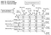
- semiconductor DRAM array 10includes a plurality of memory cells 12 each consisting of transistor 14 having gate 16 , body region 18 , which is electrically floating, source region 20 and drain region 22 .
- the body region 18is disposed between source region 20 and drain region 22 .
- body region 18is disposed on or above region 24 , which may be an insulation region (for example, in an SOI material/substrate) or non-conductive region (for example, in a bulk-type material/substrate).
- the insulation or non-conductive region 24may be disposed on substrate 26 .
- Datais written into or read from a selected memory cell by applying suitable control signals to a selected word line(s) 28 , a selected source line(s) 30 and/or a selected bit line(s) 32 .
- charge carriersare accumulated in or emitted and/or ejected from electrically floating body region 18 wherein the data states are defined by the amount of carriers within electrically floating body region 18 .
- the entire contents of the '662 patentincluding, for example, the features, attributes, architectures, configurations, materials, techniques and advantages described and illustrated therein, are incorporated by reference herein.
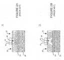
- memory cell 12 of DRAM array 10operates by accumulating in or emitting/ejecting majority carriers (electrons or holes) 34 from body region 18 of, for example, N-channel transistors.
- accumulating majority carriers (in this example, “holes”) 34 in body region 18 of memory cells 12 via, for example, impact ionization near source region 20 and/or drain region 22is representative of a logic high or “1” data state.
- Emitting or ejecting majority carriers 34 from body region 18 via, for example, forward biasing the source/body junction and/or the drain/body junctionis representative of a logic low or “0” data state. (See, FIG. 2B ).
- a logic high or State “1”corresponds to an increased concentration of majority carriers in the body region relative to an unprogrammed device and/or a device that is programmed with a logic low or State “0”.
- a logic low or State “0”corresponds to a reduced concentration of majority carriers in the body region relative to an unprogrammed device and/or a device that is programmed with logic high or State “1”.
- a floating body memory devicehas two different current states corresponding to the two different logical states: “1” and “0”.
- the memory cellis read by applying a small bias to the drain of the transistor as well as a gate bias which is above the threshold voltage of the transistor.
- a positive voltageis applied to one or more word lines 28 to enable the reading of the memory cells associated with such word lines.
- the amount of drain currentis determined/affected by the charge stored in the electrically floating body region of the transistor.
- a floating body memory cellmay have two or more different current states corresponding to two or more different logical states (for example, two different current conditions/states corresponding to the two different logical states: “1” and “0”).
- conventional writing programming techniques for memory cells having an N-channel type transistoroften provide an excess of majority carriers by channel impact ionization (see, FIG. 3A ) or by band-to-band tunneling (gate-induced drain leakage “GIDL”) (see, FIG. 3B ).
- the majority carriersmay be removed via drain side hole removal (see, FIG. 4A ), source side hole removal (see, FIG. 4B ), or drain and source hole removal, for example, using the back gate pulsing (see, FIG. 4C ).
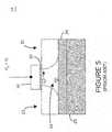
- FIG. 5illustrates the conventional reading technique.
- the state of the memory cellmay be determined by sensing the amount of the channel current provided/generated in response to the application of a predetermined voltage on the gate of the transistor of the memory cell.
- the memory cell 12 having electrically floating body transistor 14may be programmed/read using other techniques including techniques that may, for example, provide lower power consumption relative to conventional techniques.
- memory cell 12may be programmed, read and/or controlled using the techniques and circuitry described and illustrated in U.S. Non-Provisional patent application Ser. No. 11/509,188, filed on Aug. 24, 2006, and entitled “Memory Cell and Memory Cell Array Having an Electrically Floating Body Transistor, and Methods of Operating Same” (hereinafter “the '188 application”), which is incorporated by reference herein.
- the '188 applicationis directed to programming, reading and/or control methods which allow low power memory programming and provide larger memory programming window (both relative to at least the conventional programming techniques).
- the '188 applicationemploys memory cell 12 having electrically floating body transistor 14 .
- the electrically floating body transistor 14in addition to the MOS transistor, includes an intrinsic bipolar transistor (including, under certain circumstances, a significant intrinsic bipolar current).
- electrically floating body transistor 14is an N-channel device. As such, majority carriers are “holes”.
- Such control signalsinduce or cause impact ionization and/or the avalanche multiplication phenomenon. (See, FIG. 7 ).
- the predetermined voltages of the control signalsin contrast to the conventional method program or write logic “1” in the transistor of the memory cell via impact ionization and/or avalanche multiplication in the electrically floating body.
- the bipolar transistor current responsible for impact ionization and/or avalanche multiplication in the floating bodyis initiated and/or induced by a control pulse which is applied to gate 16 .
- a control pulsemay induce the channel impact ionization which increases the floating body potential and turns on the bipolar current.
- Such control signalsinduce or provide removal of majority carriers from the electrically floating body of transistor 14 . In one embodiment, the majority carriers are removed, eliminated or ejected from body region 18 through source region 20 and drain region 22 . (See, FIG. 8 ). In this embodiment, writing or programming memory cell 12 with logic “0” may again consume lower power relative to conventional techniques.
- the transistor 14 of memory cell 12may be placed in a “holding” state via application of control signals (having predetermined voltages) that are applied to gate 16 and source region 20 and drain region 22 of transistor 14 of memory cell 12 .
- control signalshaving predetermined voltages
- such control signalsprovide, cause and/or induce majority carrier accumulation in an area that is close to the interface between gate dielectric 32 and electrically floating body region 18 . (See, FIG. 9 ).
- Such signalsinduce and/or cause the bipolar transistor current in those memory cells 12 storing a logic state “1”.
- control signalsdo not induce and/or cause a considerable, substantial or sufficiently measurable bipolar transistor current in the cells programmed to “0” state.
- transistors 14 of device 10are periodically pulsed between a positive gate bias, which (1) drives majority carriers (holes for N-channel transistors) away from the interface between gate insulator 32 and body region 18 of transistor 14 and (2) causes minority carriers (electrons for N-channel transistors) to flow from source region 20 and drain region 22 into a channel formed below gate 16 , and the negative gate bias, which causes majority carriers (holes for N-channel transistors) to accumulate in or near the interface between gate 16 and body region 18 of transistor 14 .
- a positive gate biaswhich (1) drives majority carriers (holes for N-channel transistors) away from the interface between gate insulator 32 and body region 18 of transistor 14 and (2) causes minority carriers (electrons for N-channel transistors) to flow from source region 20 and drain region 22 into a channel formed below gate 16
- the negative gate biaswhich causes majority carriers (holes for N-channel transistors) to accumulate in or near the interface between gate 16 and body region 18 of transistor 14 .
- control signals having predetermined amplitudesmay be applied to memory cells 12 b and 12 c to write or program logic state “0” therein.
- the source pulsemay be applied to source region 20 of memory cells 12 b and 12 c before the gate pulse is applied to gate 16 of memory cells 12 b and 12 c , or simultaneously thereto, or after the gate pulse is applied to gate 16 of memory cells 12 b and 12 c .
- a drain pulse(0.5V amplitude in this example) is applied to drain regions 22 of memory cells 12 b and 12 d to prevent, prohibit, limit and/or retard a bipolar current (if any) from causing or generating a sufficient charge in the floating body region of memory cells 12 b and 12 c to program or write a logic state “1” into memory cells 12 b and 12 c .
- the drain pulseprevents bipolar current and the write of a logic state “1” but is not high enough to block the ejection of majority charges from the floating body region, thus a logic state “0” is written.
- the drain pulsebe applied to drain region 22 of memory cells 12 b and 12 c for a temporal period that extends or is applied before, during and after the source and gate pulses (for example, initiates, starts, ramps, declines and/or terminates) as illustrated in FIG. 11 .
- a holding conditionmay be applied or established to prevent, minimize or avoid disturbance of the data state of, or charge stored in the unselected memory cells.
- a voltagefor example, ⁇ 1.2V
- a voltagefor example, 0V
- source regions 20 and drain regions 22 of the unselected memory cellsto prevent, minimize or avoid disturbance of the data state in the unselected memory cells during the programming or writing operation.
- the data state of the unselected memory cellsis unaffected (or substantially unaffected) by the programming of or writing to selected memory cells 12 a - d.
- control signals having a predetermined amplitudemay be selectively applied to a row of memory cells (for example, memory cells 12 a - d ) to read the data state in each of the selected memory cells 12 a - 12 d .
- a voltage pulse of 3Vmay be applied to source region 20
- a voltage pulse of ⁇ 0.5Vmay be applied to gate 16 of memory cells 12 a - d .
- the source pulsemay be applied to source region 20 before application of the gate pulse to gate 16 , simultaneously thereto, or after the gate pulse is applied to gate 16 . Further, the source pulse may cease or terminate before the gate pulse, simultaneously thereto (as illustrated in FIG. 11 ), or after the gate pulse concludes or ceases.
- a holding conditionmay be applied or established to prevent, minimize or avoid disturbance of the data state in the unselected memory cells.
- a voltagefor example, ⁇ 1.2V
- a voltagefor example, 0V
- source regions 20 of the unselected memory cellsto prevent, minimize or avoid disturbance of the data state in the unselected memory cells during the read operation.
- the illustrated/exemplary voltage levels to implement the write and read operations, with respect to the '188 applicationare merely exemplary.
- the indicated source, drain or gate voltages)become or are positive and negative.
- the present inventionsare directed to an integrated circuit device (for example, a logic or discrete memory device) comprising a memory cell array having a plurality of word lines, a plurality of source lines, a plurality of bit lines, and a plurality of memory cells arranged in a matrix of rows and columns, wherein each memory cell includes an electrically floating body transistor.
- the electrically floating body transistor(for example, an N-channel type transistor or a P-channel type transistor) includes a first region coupled to an associated source line, a second region coupled to an associated bit line, a body region disposed between the first region and the second region, wherein the body region is electrically floating, and a gate disposed over the body region and coupled to an associated word line.
- the memory cellincludes a plurality of data states, including (i) a first data state which is representative of a first charge in the body region of the electrically floating body transistor and (ii) a second data state which is representative of a second charge in the body region of the electrically floating body transistor.
- the integrated circuit device of this aspectfurther includes first circuitry, coupled to each memory cell of a first row of memory cells, to concurrently apply (i) write control signals to a first group of memory cells of the first row of memory cells to write one of the plurality of data states therein, and (ii) write de-select control signals to a second group of memory cells of the first row of memory cells to inhibit writing of write one of the plurality of data states therein.
- the number of memory cells of the first group of memory cellsmay correspond to a word length of the memory cell array.
- the integrated circuit deviceincludes word length selection circuitry (for example, fuses or anti-fuses, or DRAM, SRAM, ROM, PROM, EPROM, EEPROM cells, latches, registers, and/or fixed via, for example, voltages applied to signal lines or pins) to store data which is representative of the word length.
- word length selection circuitryfor example, fuses or anti-fuses, or DRAM, SRAM, ROM, PROM, EPROM, EEPROM cells, latches, registers, and/or fixed via, for example, voltages applied to signal lines or pins
- the write de-select control signalsinclude: (i) a first temporally changing signal applied to the gate of each memory cell of the second group of memory cells, (ii) a second temporally changing signal applied to the first region of each memory cell of the second group of memory cells, and (iii) a third temporally changing signal applied to the second region of each memory cell of the second group of memory cells.
- the write control signalsmay include: (i) the first temporally changing signal applied to the gate of each memory cell of the first group of memory cells, (ii) the second temporally changing signal applied to the first region of each memory cell of the first group of memory cells, and (iii) a fourth temporally changing signal applied to the second region of each memory cell of the first group of memory cells.
- the write de-select control signalsinclude: (i) a first temporally changing signal applied to the gate of each memory cell of the second group of memory cells, (ii) a second temporally changing signal applied to the first region of each memory cell of the second group of memory cells, and (iii) a third signal having a substantially constant voltage amplitude applied to the second region of each memory cell of the second group of memory cells.
- the write control signalsmay include: (i) the first temporally changing signal applied to the gate of each memory cell of the first group of memory cells, (ii) the second temporally changing signal applied to the first region of each memory cell of the first group of memory cells, and (iii) a fourth temporally changing signal applied to the second region of each memory cell of the first group of memory cells.
- the integrated circuit devicemay further include second circuitry, coupled to each memory cell of the first row of memory cells, to concurrently apply: (i) read control signals to the first group of memory cells of the first row of memory cells to read the data state of each memory cell of the first group of memory cells, and (ii) read de-select control signals to the second group of memory cells of the first row of memory cells to inhibit reading the data state of each memory cell of the second group of memory cells.
- second circuitrycoupled to each memory cell of the first row of memory cells, to concurrently apply: (i) read control signals to the first group of memory cells of the first row of memory cells to read the data state of each memory cell of the first group of memory cells, and (ii) read de-select control signals to the second group of memory cells of the first row of memory cells to inhibit reading the data state of each memory cell of the second group of memory cells.
- the read control signalsmay include a signal applied to the gate, a signal applied to the first region, and a signal applied to the second region of the electrically floating body transistor of each memory cell of the first group of memory cells to cause, memory cell substantially based on the read bipolar transistor current.
- the second circuitrymay include a plurality of sense amplifiers.
- the write control signalsinclude control signals to write the first data state and wherein, in response to the control signals to write the first data state into a predetermined memory cell of the first row of memory cells, the electrically floating body transistor of the predetermined memory cell of the first row of memory cells generates a bipolar transistor current which substantially provides the first charge in the body region of the electrically floating body transistor of the predetermined memory cell of the first row of memory cells.
- the memory cellsmay store more than one data bit (for example, two, three, four, five, six, etc.) and/or more than two data states (for example, three, four, five, six, etc. data or logic states).
- each memory cell of the memory cell arraymay include a third data state which is representative of a third charge in the body region of the electrically floating body transistor.
- the present inventionsare directed to an integrated circuit device (for example, a logic or discrete memory device) comprising a memory cell array having a plurality of word lines, a plurality of source lines, a plurality of bit lines, and a plurality of memory cells arranged in a matrix of rows and columns, wherein each memory cell includes an electrically floating body transistor.
- the electrically floating body transistor(for example, an N-channel type transistor or a P-channel type transistor) includes a first region coupled to an associated source line, a second region coupled to an associated bit line, a body region disposed between the first region and the second region, wherein the body region is electrically floating, and a gate disposed over the body region and coupled to an associated word line.
- the memory cellincludes a plurality of data states, including (i) a first data state which is representative of a first charge in the body region of the electrically floating body transistor and (ii) a second data state which is representative of a second charge in the body region of the electrically floating body transistor.
- the integrated circuit device of this aspectfurther includes circuitry (for example, a plurality of sense amplifiers), coupled to each memory cell of the first row of memory cells, to substantially concurrently apply: (i) read control signals to a first group of memory cells of the first row of memory cells to read the data state of each memory cell of the first group of memory cells, and (ii) read de-select control signals to a second group of memory cells of the first row of memory cells to inhibit reading the data state of each memory cell of the second group of memory cells.
- circuitryfor example, a plurality of sense amplifiers
- the read control signalsinclude a signal applied to the gate, a signal applied to the first region, and a signal applied to the second region of the electrically floating body transistor of each memory cell of the first group of memory cells to cause, force and/or induce a read bipolar transistor current which is representative of the data state of each memory cell of the first group of memory cells of the first row of memory cells.
- the circuitrymay determine the data state of the memory cell substantially based on the read bipolar transistor current.
- the integrated circuit devicemay further include write circuitry, coupled to each memory cell of a first row of memory cells, to concurrently apply: (i) write control signals to a first group of memory cells of the first row of memory cells to write one of the plurality of data states therein, and (ii) write de-select control signals to a second group of memory cells of the first row of memory cells to inhibit the writing of write one of the plurality of data states therein.
- the write control signalsinclude control signals to write the first data state and wherein, in response to the control signals to write the first data state into a predetermined memory cell of the first row of memory cells, the electrically floating body transistor of the predetermined memory cell of the first row of memory cells generates a bipolar transistor current which substantially provides the first charge in the body region of the electrically floating body transistor of the predetermined memory cell of the first row of memory cells.
- the number of memory cells of the first group of memory cellsmay correspond to a word length of the memory cell array.
- the integrated circuit deviceincludes word length selection circuitry (for example, fuses or anti-fuses, or DRAM, SRAM, ROM, PROM, EPROM, EEPROM cells, latches, registers, and/or fixed via, for example, voltages applied to signal lines or pins) to store data which is representative of the word length.
- word length selection circuitryfor example, fuses or anti-fuses, or DRAM, SRAM, ROM, PROM, EPROM, EEPROM cells, latches, registers, and/or fixed via, for example, voltages applied to signal lines or pins
- the present inventionsare directed to an integrated circuit device (for example, a logic or discrete memory device) comprising a semiconductor memory array, disposed in or on a semiconductor region or layer which resides on or above an insulating region or layer of a substrate.
- the semiconductor memory arrayincludes a plurality of word lines, a plurality of source lines, a plurality of bit lines, and a plurality of memory cells arranged in a matrix of rows and columns, wherein each memory cell includes an electrically floating body transistor.
- the electrically floating body transistor(for example, an N-channel type transistor or a P-channel type transistor) includes a first region coupled to an associated source line, a second region coupled to an associated bit line, a body region disposed between the first region and the second region, wherein the body region is electrically floating, and a gate disposed over the body region and coupled to an associated word line.
- the memory cellincludes a plurality of data states, including (i) a first data state which is representative of a first charge in the body region of the electrically floating body transistor and (ii) a second data state which is representative of a second charge in the body region of the electrically floating body transistor.
- the integrated circuit device of this aspectalso includes first circuitry, coupled to each memory cell of a first row of memory cells, to concurrently apply (i) write control signals to a first group of memory cells of the first row of memory cells to write one of the plurality of data states therein, and (ii) write de-select control signals to a second group of memory cells of the first row of memory cells to inhibit writing of write one of the plurality of data states therein
- the integrated circuit device of this aspectfurther includes second circuitry (for example, a plurality of sense amplifiers), coupled to each memory cell of the first row of memory cells, to substantially concurrently apply: (i) read control signals to a first group of memory cells of the first row of memory cells to read the data state of each memory cell of the first group of memory cells, and (ii) read de-select control signals to a second group of memory cells of the first row of memory cells to inhibit reading the data state of each memory cell of the second group of memory cells.
- second circuitryfor example, a plurality of sense amplifiers
- the read control signalsinclude a signal applied to the gate, a signal applied to the first region, and a signal applied to the second region of the electrically floating body transistor of each memory cell of the first group of memory cells to cause, force and/or induce a read bipolar transistor current which is representative of the data state of each memory cell of the first group of memory cells of the first row of memory cells.
- the second circuitrydetermines the data state of the memory cell substantially based on the read bipolar transistor current.
- the write control signalsinclude control signals to write the first data state and wherein, in response to the control signals to write the first data state into a predetermined memory cell of the first row of memory cells, the electrically floating body transistor of the predetermined memory cell of the first row of memory cells generates a bipolar transistor current which substantially provides the first charge in the body region of the electrically floating body transistor of the predetermined memory cell of the first row of memory cells.
- the number of memory cells of the first group of memory cellsmay correspond to a word length of the memory cell array.
- the integrated circuit deviceincludes word length selection circuitry (for example, fuses or anti-fuses, or DRAM, SRAM, ROM, PROM, EPROM, EEPROM cells, latches, registers, and/or fixed via, for example, voltages applied to signal lines or pins) to store data which is representative of the word length.
- word length selection circuitryfor example, fuses or anti-fuses, or DRAM, SRAM, ROM, PROM, EPROM, EEPROM cells, latches, registers, and/or fixed via, for example, voltages applied to signal lines or pins
- the memory cellsmay store more than one data bit (for example, two, three, four, five, six, etc.) and/or more than two data states (for example, three, four, five, six, etc. data or logic states).
- each memory cell of the memory cell arraymay include a third data state which is representative of a third charge in the body region of the electrically floating body transistor.
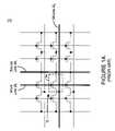
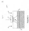
- FIG. 1Ais a schematic representation of a prior art DRAM array including a plurality of memory cells comprised of one electrically floating body transistor;
- FIG. 1Bis a three dimensional view of an exemplary prior art memory cell comprised of one electrically floating body transistor (PD-SOI NMOS);
- PD-SOI NMOSelectrically floating body transistor
- FIG. 1Cis a cross-sectional view of the prior art memory cell of FIG. 1B , cross-sectioned along line C-C′;
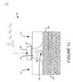
- FIGS. 2A and 2Bare exemplary schematic illustrations of the charge relationship, for a given data state, of the floating body, source and drain regions of a prior art memory cell comprised of one electrically floating body transistor (PD-SOI NMOS);
- PD-SOI NMOSelectrically floating body transistor
- FIGS. 3A and 3Bare exemplary schematic and general illustrations of conventional methods to program a memory cell to logic state “1” (i.e., generate or provide an excess of majority carrier in the electrically floating body of the transistor (an N-type channel transistor in this exemplary embodiment) of the memory cell of FIG. 1B ; majority carriers in these exemplary embodiments are generated or provided by the channel electron impact ionization ( FIG. 3A ) and by GIDL or band to band tunneling (FIG. 3 B));
- FIGS. 4A-4Care exemplary schematics and general illustrations of conventional methods to program a memory cell to logic state “0” (i.e., provide relatively fewer majority carriers by removing majority carriers from the electrically floating body of the transistor of the memory cell of FIG. 1B ; majority carriers may be removed through the drain region/terminal of the transistor ( FIG. 4A ), the source region/terminal of the transistor ( FIG. 4B ), and through both drain and source regions/terminals of the transistor by using, for example, the back gate pulses applied to the substrate/backside terminal of the transistor of the memory cell (FIG. 4 C));
- FIG. 5illustrates an exemplary schematic (and control signal) of a conventional reading technique
- the state of the memory cellmay be determined by sensing the amount of the channel current provided/generated in response to the application of a predetermined voltage on the gate of the transistor of the memory cell;
- FIG. 6is a schematic representation of an equivalent electrically floating body memory cell (N-channel type) including an intrinsic bipolar transistor in addition to the MOS transistor;
- FIG. 7illustrates an exemplary schematic (and control signal voltage relationship) of an exemplary embodiment of an aspect of the '188 application of programming a memory cell to logic state “1” by generating, storing and/or providing an excess of majority carriers in the electrically floating body of the transistor of the memory cell;
- FIG. 8illustrates an exemplary schematic (and control signals) of an exemplary embodiment of an aspect of the '188 application of programming a memory cell to a logic state “0” by generating, storing and/or providing relatively fewer majority carriers (as compared to the number of majority carriers in the electrically floating body of the memory cell that is programmed to a logic state “1”) in the electrically floating body of the transistor of the memory cell, wherein the majority carriers are removed (write “0”) through both drain and source terminals by applying a control signal (for example, a programming pulse) to the gate of the transistor of the memory cell;
- a control signalfor example, a programming pulse
- FIG. 9illustrates an exemplary schematic (and control signals) of an exemplary embodiment of an aspect of the '188 application of holding or maintaining the data state of a memory cell
- FIG. 10illustrates an exemplary schematic (and control signals) of an exemplary embodiment of an aspect of the '188 application of reading the data state of a memory cell by sensing the amount of the current provided/generated in response to an application of a predetermined voltage on the gate of the transistor of the memory cell;
- FIG. 11illustrates exemplary timing relationships of selected write control signals to (i) program or write a logic state “1” into one or more N-channel type memory cells, (ii) program or write logic state “0” into one or more N-channel type memory cells, and (iii) read one or more N-channel type memory cells according to one embodiment of the inventions described and illustrated in the '188 application;
- FIGS. 12 and 13illustrate an exemplary embodiment of a memory array having a plurality of memory cells (N-channel type) and employing a separated source line configuration for each row of memory cells in conjunction with exemplary programming techniques, including exemplary control signal voltage values ( FIG. 11 ) and exemplary reading techniques, including exemplary control signal voltage values ( FIG. 12 ), according to certain aspects of the inventions described and illustrated in the '188 application;
- FIG. 14illustrates exemplary timing relationships of selected write control signals to (i) program or write a logic state “1” into one or more P-channel type memory cells, (ii) program or write logic state “0” into one or more P-channel type memory cells, and (iii) read one or more P-channel type memory cells according to one embodiment of the '188 application;
- FIG. 15illustrates an exemplary embodiment of a memory array employing a common source line configuration for each row of memory cells in conjunction with control signal voltages to write/program selected memory cells of a selected row of memory cells and control voltages to de-select or “block” the write/program operation of unselected memory cells of the selected row of memory cells, in accordance with certain aspect of the present inventions;
- FIG. 16illustrates an exemplary embodiment of a memory array employing a common source line configuration for each row of memory cells in conjunction with control signal voltages to read the data state of selected memory cells of a selected row of memory cells and control voltages to de-select or “block” the read operation of unselected memory cells of the selected row of memory cells, in accordance with certain aspect of the present inventions;
- FIGS. 17 , 18 , and 19illustrate exemplary timing relationships of selected write control signals to (i) de-select, program or write of logic state “1” into one or more N-channel type memory cells, (ii) de-select, program or write of logic state “0” into one or more N-channel type memory cells, and (iii) de-select or read of one or more N-channel type memory cells, in accordance with certain aspect of the present inventions, wherein the de-select control signal includes a pulsed characteristic (see, FIG. 17 ) and a non-pulsed characteristic (see, FIGS. 18 and 19 );
- FIGS. 20A-20Care schematic block diagram illustrations of exemplary integrated circuit devices in which the memory cell array (and certain peripheral circuitry) may be implemented, according to one or more aspects of the present inventions;
- FIGS. 20D and 20Eare schematic block diagrams of embodiments of an integrated circuit device including, among other things, a memory cell array, data sense and write circuitry, memory cell selection and control circuitry, according to one or more aspects of the present inventions.
- FIGS. 21A-21Care schematic representations of exemplary architectures and/or embodiments of implementing a controller/processor in conjunction with memory devices having a programmable word length, in accordance with one or more aspects of the present inventions.
- the present inventionsare directed to techniques for reading, controlling and/or operating a semiconductor memory cell, array, architecture and device (i.e., an integrated circuit device, for example, a logic device (such as, a microcontroller or microprocessor) or a memory device (such as, a discrete memory)) including electrically floating body transistors in which electrical charge is stored in the body of the transistor.
- a semiconductor memory cell, array, architecture and devicei.e., an integrated circuit device, for example, a logic device (such as, a microcontroller or microprocessor) or a memory device (such as, a discrete memory)
- the present inventionsare also directed to semiconductor memory cell, array, architecture and device that include circuitry to implement such reading, controlling and/or operating techniques.
- the word length (which relates to the selected memory cells of a given/predetermined selected row of memory cells) of the memory cell arrayis variable and/or programmable.
- the word lengthmay be an amount equal to any number of memory cells of a selected row which is less than or equal to the total number of memory cells of the selected row of the memory array.
- write and/or read operationsmay be performed with respect to selected memory cells (i.e., a first group of memory cells) of a selected row of the memory array, while unselected memory cells (i.e., a second group of memory cells) of the selected row are undisturbed.
- exemplary control signals having predetermined amplitudemay be selectively applied (based on address data) to a given/predetermined row of memory cells (for example, memory cells 12 a - d which are connected to the same word line, namely word line 28 i ) to write logic state “1” into selected memory cell 12 a , and logic state “0” into selected memory cell 12 b .
- exemplary “write de-select” control signalshaving predetermined amplitude, are applied to unselected memory cells 12 c and 12 d to prevent, inhibit and/or disable the write operation so that memory cells 12 c and 12 d of the selected row of memory cells remain in their existing memory states “0” and “1”, respectively.
- a “write de-select” voltage pulseis applied to bit lines 32 j+2 and 32 j+3 to prevent, inhibit and/or disable the write operation with respect to memory cells 12 c and 12 d by preventing, minimizing, eliminating and/or blocking charge loss for the case of a cell previously written to logic state “1” (here, memory cell 12 c ), or preventing, minimizing, eliminating bipolar current generation for the case of a cell previously written to logic state “0” (here, memory cell 12 d ).
- the de-select control signalsmay be applied to bit lines 32 j+2 and 32 j+3 as a voltage pulse, as illustrated in FIG. 17 , during the write operation or may be applied continuously to bit lines 32 j+2 and 32 j+3 , as illustrated in FIG. 18 .
- control signalshaving predetermined amplitude, are selectively applied (based on address data) to a predetermined or given row of memory cells (for example, memory cells 12 a - d which are connected to the same word line, namely word line 28 i ) to read selected memory cells 12 a and 12 b .
- exemplary “read de-select” control signalshaving predetermined amplitude, are applied to unselected memory cells 12 c and 12 d to prevent, inhibit and/or disable the read operation so that memory cells 12 c and 12 d of the selected row of memory cells are not impacted by the read operation.
- a “read de-select” voltage pulse or constant voltageis applied to bit lines 32 j+2 and 32 j+3 to prevent, inhibit and/or disable the read operation with respect to memory cells 12 c and 12 d —notwithstanding that such memory cells are a portion of the selected row of memory cells.
- memory cells 12 c and 12 dare not read, impacted and/or adversely affected by the read operation.
- memory cells 12 c and 12 ddo not significantly conduct current during a read operation and are not disturbed—not withstanding the access of the row of memory cells via word line 28 i .
- the voltage amplitudes illustrated in FIGS. 15-19 (among others) to perform selected operationsare merely exemplary.
- the indicated voltage levelsmay be relative or absolute.
- the voltages indicatedmay be relative in that each voltage level, for example, may be increased or decreased by a given voltage amount (for example, each voltage may be increased/decreased by 0.25, 0.5, 1.0 and 2.0 volts (or more)) whether one or more of the voltages (for example, the source, drain or gate voltages) become or are positive and negative.
- the present inventionsmay have several advantages over prior art techniques which typically include a long row memory cell array for area efficiency with pipeline techniques because of the resulting difference between array word length and input/output word length. Because with the present inventions, the selected memory cells of the selected row are written or read and unselected memory cells of the selected row are not adversely affected by the predetermined operation, the word length of the memory array may be the same as the input/output word length in spite of maintaining a long row memory cell array for area efficiency.
- the selected memory cells of the selected rowis written or read (while the unselected memory cells of the selected row do not participate in or are not adversely affected by the operation) so in cases where data addresses are not consecutive and pipeline techniques are not effective, power management is enhanced because the unselected memory cells (which are presumably not needed) are not read from during the read operation or written into during the write operation.
- memory cell array word length and input/output word lengthare the same, data may be written into or read from the memory array in a single step or stage which may provide for faster operation and/or lower power consumption.
- conventional techniquesoften employ a two step or stage write to first write data into latches and then write data from latches to memory cells.
- datais first read from the memory cell array into latches and thereafter to the output.
- the present inventionsalso allow the word length to be changed between operations at any time, for example, by control of the data write and sense circuitry and memory cell selection and control circuitry.
- the word lengthmay be set and/or controlled, for example, at fabrication, during test, and/or in situ.
- the integrated circuit devicemay be programmed (i) after power-up, for example, during an initialization phase, or (ii) during operation to minimize power consumption and maximize speed.
- the word length of the random accessesmay be set to match the I/O width for maximum speed.
- a word lengthmay be set to equal the number of physical bits on a row so data would first be written to latches and then written to an entire row in one operation for lower power consumption.
- Consecutive data addressesmay be indicated by an external input to the memory of the integrated circuit, or consecutive addresses could be detected internal to the memory of the integrated circuit. With respect to refresh operations for which no data is input or output from the memory but all bits on a row must be refreshed, a word length equal to the number of physical bits on a row may be set. In this way, power consumption may be reduced and/or minimized.
- word length of the memory array of the integrated circuitmay be one time programmable (for example, programmed during test or at manufacture) or more than one time programmable (for example, during test, start-up/power-up, during an initialization sequence and/or during operation (in situ)).
- the word lengthmay be “stored” in word length selection circuitry that resides on the integrated circuit (for example, fuses or anti-fuses, or DRAM, SRAM, ROM, PROM, EPROM, EEPROM cells, latches, registers, and/or fixed via, for example, voltages applied to signal lines or pins). (See, for example, FIGS. 20C and 20D ).
- any programming technique and/or circuitryare intended to fall within the scope of the present inventions.
- the control circuitry to determine, implement and/or program the word lengthmay be implemented on-chip, which is resident on (i.e., integrated in) the device, or off-chip (i.e., disposed on or in a different integrated circuit device, for example, disposed on/in a memory controller, microprocessor and/or graphics processor).
- the control circuitrymay implement any programming technique and/or circuitry, whether now known or later developed; all such techniques and circuitry are intended to fall within the scope of the present inventions.
- the memory cell and/or memory cell array, as well as the circuitry of the present inventionsmay be implemented in an integrated circuit device having a memory portion and a logic portion (see, for example, FIGS. 20A and 20C ), or an integrated circuit device that is primarily a memory device (see, for example, FIG. 20B ).
- the memory arraymay include a plurality of memory cells arranged in a plurality of rows and columns wherein each memory cell includes an electrically floating body transistor.
- the memory arraysmay be comprised of N-channel, P-channel and/or both types of transistors.
- circuitry that is peripheral to the memory arraymay include P-channel and/or N-channel type transistors.
- the integrated circuit devicemay include array 10 , having a plurality of memory cells 12 , data write and sense circuitry, and memory cell selection and control circuitry.
- the data write and sense circuitryreads data from and writes data to selected memory cells 12 .
- the data write and sense circuitryincludes a plurality of data sense amplifiers. Each data sense amplifier receives at least one bit line 32 and an output of reference generator circuitry (for example, a current or voltage reference signal).
- the data sense amplifiermay be one or more of the cross-coupled type sense amplifiers like the cross-coupled type sense amplifier described and illustrated in the Non-Provisional U.S. patent application Ser. No. 11/299,590 (U.S.
- Patent Application Publication US 2006/0126374filed by Waller and Carman, on Dec. 12, 2005, and entitled “Sense Amplifier Circuitry and Architecture to Write Data into and/or Read Data from Memory Cells”, the application being incorporated herein by reference in its entirety) to sense the data state stored in memory cell 12 and/or write-back data into memory cell 12 .
- the present inventionsmay be implemented in any electrically floating body memory cell and memory cell array.
- the present inventionsare a memory array, having a plurality of memory cells each including an electrically floating body transistor, and/or technique of writing or programming data into one or more memory cells of such a memory array.
- the data states of adjacent memory cells and/or memory cells that share a word linemay be individually programmed.
- the present inventionshas been described, by way of example, in the context of an embodiment of the '188 application, the present inventions may be implemented in or with other memory cell and memory array technologies, for example, 1T-1C (one transistor, one capacitor) and electrically floating gate memory cells.
- the memory arraysmay be comprised of N-channel, P-channel and/or both types of transistors. Indeed, circuitry that is peripheral to the memory array (for example, sense amplifiers or comparators, row and column address decoders, as well as line drivers (not illustrated herein)) may include P-channel and/or N-channel type transistors.
- the datamay be read from P-channel type memory cells by applying a voltage pulse of ⁇ 3V to the source region, and a voltage pulse of 0.5V may be applied to the gate of the memory cells to be read.
- the source pulsemay be applied to the source region before application of the gate pulse to the gate, simultaneously thereto, or after the gate pulse is applied the gate. Further, the source pulse may cease or terminate before the gate pulse, simultaneously thereto (as illustrated in FIG. 14 ), or after the gate pulse concludes or ceases.
- circuitry and techniques of the present inventionsmay be employed in conjunction with any electrically floating body memory cell (i.e., a memory cell including at least one electrically floating body transistor), and/or architecture, layout, structure and/or configuration employing such electrically floating body memory cells (among other types of memory cells).
- any electrically floating body memory celli.e., a memory cell including at least one electrically floating body transistor
- architecture, layout, structure and/or configurationemploying such electrically floating body memory cells (among other types of memory cells).
- an electrically floating body transistorwhose state is read, programmed and/or controlled using the techniques of the present inventions, may be implemented in the memory cell, architecture, layout, structure and/or configuration described and illustrated in the following provisional and non-provisional U.S. patent applications:
- the memory cellsmay be controlled (for example, programmed or read) using any of the control circuitry described and illustrated in the above-referenced eleven (11) U.S. patent applications.
- the control circuitrydescribed and illustrated in the above-referenced eleven (11) U.S. patent applications.
- those discussionswill not be repeated and are incorporated herein by reference. Indeed, all memory cell selection and control circuitry, and techniques for programming, reading, controlling and/or operating memory cells including transistors having electrically floating body regions, whether now known or later developed, are intended to fall within the scope of the present inventions.
- the data stored in or written into memory cells 12 of DRAM array/device 10may be read using well known circuitry and techniques (whether conventional or not), including those described in the above-referenced eleven (11) U.S. patent applications.
- the present inventionsmay also employ the read circuitry and techniques described and illustrated in U.S. patent application Ser. No. 10/840,902, which was filed by Portmann et al. on May 7, 2004, and entitled “Reference Current Generator, and Method of Programming, Adjusting and/or Operating Same” (now U.S. Pat. No. 6,912,150).
- the present inventionsmay employ the read operation techniques described and illustrated in U.S. patent application Ser. No. 11/515,667, which was filed by Bauser on Sep. 5, 2006, and entitled “Method and Circuitry to Generate a Reference Current for Reading a Memory Cell, and Device Implementing Same”.
- the entire contents of the U.S. patent application Ser. No. 11/515,667, as noted above,are incorporated herein by reference.
- a sense amplifier(not illustrated in detail) may be employed to read the data stored in memory cells 12 .
- the sense amplifiermay sense the data state stored in memory cell 12 using voltage or current sensing techniques.
- the current sense amplifiermay compare the cell current to a reference current, for example, the current of a reference cell (not illustrated). From that comparison, it may be determined whether memory cell 12 contained a logic high (relatively more majority carriers 34 contained within body region 18 ) or logic low data state (relatively less majority carriers 34 contained within body region 18 ).
- the electrically floating memory cells, transistors and/or memory array(s)may be fabricated using well known techniques and/or materials. Indeed, any fabrication technique and/or material, whether now known or later developed, may be employed to fabricate the electrically floating body memory cells, transistors and/or memory array(s).
- the present inventionsmay employ silicon (whether bulk-type or SOI), germanium, silicon/germanium, gallium arsenide or any other semiconductor material in which transistors may be formed.
- the electrically floating transistors, memory cells, and/or memory array(s)may employ the techniques described and illustrated in non-provisional patent application entitled “Integrated Circuit Device, and Method of Fabricating Same”, which was filed on Jul. 2, 2004, by Fazan, Ser. No.
- memory array 10may be integrated with SOI logic transistors, as described and illustrated in the Integrated Circuit Device Patent Applications.
- an integrated circuit deviceincludes memory section (having, for example, PD or FD SOI memory transistors 14 ) and logic section (having, for example, high performance transistors, such as FinFET, multiple gate transistors, and/or non-high performance transistors (for example, single gate transistors that do not possess the performance characteristics of high performance transistors—not illustrated)).
- memory sectionhaving, for example, PD or FD SOI memory transistors 14
- logic sectionhaving, for example, high performance transistors, such as FinFET, multiple gate transistors, and/or non-high performance transistors (for example, single gate transistors that do not possess the performance characteristics of high performance transistors—not illustrated)).
- the entire contents of the Integrated Circuit Device Patent Applicationsincluding, for example, the inventions, features, attributes, architectures, configurations, materials, techniques and advantages described and illustrated therein, are hereby incorporated by reference.
- the memory arraysmay be comprised of N-channel, P-channel and/or both types of transistors, as well as partially depleted and/or fully depleted type transistors.
- circuitry that is peripheral to the memory arraymay include fully depleted type transistors (whether P-channel and/or N-channel type).
- circuitrymay include partially depleted type transistors (whether P-channel and/or N-channel type).
- electrically floating body transistor 14may be a symmetrical or non-symmetrical device. Where transistor 14 is symmetrical, the source and drain regions are essentially interchangeable. However, where transistor 14 is a non-symmetrical device, the source or drain regions of transistor 14 have different electrical, physical, doping concentration and/or doping profile characteristics. As such, the source or drain regions of a non-symmetrical device are typically not interchangeable. This notwithstanding, the drain region of the electrically floating N-channel transistor of the memory cell (whether the source and drain regions are interchangeable or not) is that region of the transistor that is connected to the bit line/sense amplifier.
- the plurality of memory cells 12 of the present inventionsmay be implemented in any memory array having, for example, a plurality of rows and columns (for example, in a matrix form).
- the present inventionsmay be implemented in any electrically floating body memory cell and memory cell array.
- the present inventionsmay be implemented in other memory cell and memory array technologies, for example, 1T-1C (one transistor, one capacitor) and electrically floating gate memory cells.
- a holding conditionmay be applied or established to prevent, minimize or avoid disturbance of the data state of, or charge stored in the memory cells of the unselected rows of memory cells.
- a voltagefor example, ⁇ 1.2V
- a voltagefor example, 0V
- the data state of the memory cells of the unselected rows of memory cellsis unaffected (or substantially unaffected) by the programming of or writing to selected memory cells of the selected rows. (See, for example, FIG. 15 ).
- a holding conditionmay be applied or established to prevent, minimize or avoid disturbance of the data state in the memory cells of the unselected rows of memory cells of the array.
- a voltagefor example, ⁇ 1.2V
- a voltagefor example, 0V
- the states of the memory cells of the unselected rows of memory cellsare unaffected (or it is substantially unaffected) during the reading of selected memory cells of the selected rows of memory cells. (See, for example, FIG. 16 ).
- the word length of the arraymay be one time programmable (for example, programmed during test, design or at manufacture) or more than one time programmable (for example, during test, start-up/power-up, during an initialization sequence and/or during operation (in situ)).
- data which is representative of the word lengthmay be stored in on-chip word length selection circuitry (for example, in fuses or anti-fuses, or DRAM, SRAM, ROM, PROM, EPROM, EEPROM cells, latches, and/or registers which is/are resident on or integrated in the device).
- the on-chip word length selection circuitrymay be disposed, in whole or in part, in the logic portion and/or peripheral portion of the integrated circuit device. (See, for example, FIGS. 20A-20C ).
- word length selection circuitrymay be located, in whole or in part, on-chip (for example, in fuses or anti-fuses, or DRAM, SRAM, ROM, PROM, EPROM, EEPROM cells, latches, and/or registers) and the circuitry that programs such word length selection circuitry may be located off-chip.
- word length selection circuitry(which, in this embodiment, is on-chip) may be programmed via circuitry located or disposed in external controller/processor 36 (for example, memory controller, microprocessor and/or graphics processor).
- the external controller/processor 36may be implemented on module 100 (see, for example, FIG.
- controller/processor 36may provide information to memory device 50 which, in response, controls the word length of the array within memory device 50 .
- the illustrated/exemplary voltage levels to implement the read and write operationsare merely exemplary.
- the indicated voltage levelsmay be relative or absolute.
- the voltages indicatedmay be relative in that each voltage level, for example, may be increased or decreased by a given voltage amount (for example, each voltage may be increased or decreased by 0.1, 0.15, 0.25, 0.5, 1 volt, (or more)) whether one or more of the voltages (for example, the source, drain or gate voltages) become or are positive and negative.
- circuitmay mean, among other things, a single component or a multiplicity of components (whether in integrated circuit form or otherwise), which are active and/or passive, and which are coupled together to provide or perform a desired operation.
- circuitrymay mean, among other things, a circuit (whether integrated or otherwise), or a group of circuits (whether integrated or otherwise).
- inhibitmay mean, among other things, prevent, thwart, inhibit and/or disable.
- to senseor similar, means, for example, to measure, to sample, to sense, to inspect, to detect, to monitor and/or to capture.
Landscapes
- Engineering & Computer Science (AREA)
- Microelectronics & Electronic Packaging (AREA)
- Computer Hardware Design (AREA)
- Semiconductor Memories (AREA)
- Read Only Memory (AREA)
- Non-Volatile Memory (AREA)
- Dram (AREA)
Abstract
Description
- This application claims priority to U.S. Provisional Application Ser. No. 60/790,111, entitled “Memory Array Having a Programmable Word Length, and Technique of Implementing Same”, filed Apr. 7, 2006; the contents of this provisional application are incorporated by reference herein in its entirety.
- The present inventions relate to a memory cell, array, architecture and device, and techniques for reading, controlling and/or operating such cell and device; and more particularly, in one aspect, to a semiconductor dynamic random access memory (“DRAM”) cell, array, architecture and/or device wherein the memory cell includes a transistor having an electrically floating body in which an electrical charge is stored.
- There is a continuing trend to employ and/or fabricate advanced integrated circuits using techniques, materials and devices that improve performance, reduce leakage current and enhance overall scaling. Semiconductor-on-Insulator (SOI) is a material in which such devices may be fabricated or disposed on or in (hereinafter collectively “on”). Such devices are known as SOI devices and include, for example, partially depleted (PD), fully depleted (FD) devices, multiple gate devices (for example, double or triple gate), and Fin-FET.
- One type of dynamic random access memory cell is based on, among other things, the electrically floating body effect of SOI transistors. (See, for example, U.S. Pat. No. 6,969,662, incorporated herein by reference). In this regard, the dynamic random access memory cell may consist of a PD or a FD SOI transistor (or transistor formed in bulk material/substrate) having a channel, which is interposed between the body and the gate dielectric. The body region of the transistor is electrically floating in view of the insulation layer (or non-conductive region, for example, in a bulk-type material/substrate) disposed beneath the body region. The state of memory cell is determined by the concentration of charge within the body region of the SOI transistor.
- With reference to
FIGS. 1A ,1B and1C, in one embodiment,semiconductor DRAM array 10 includes a plurality ofmemory cells 12 each consisting oftransistor 14 havinggate 16,body region 18, which is electrically floating,source region 20 anddrain region 22. Thebody region 18 is disposed betweensource region 20 and drainregion 22. Moreover,body region 18 is disposed on or aboveregion 24, which may be an insulation region (for example, in an SOI material/substrate) or non-conductive region (for example, in a bulk-type material/substrate). The insulation or non-conductiveregion 24 may be disposed onsubstrate 26. - Data is written into or read from a selected memory cell by applying suitable control signals to a selected word line(s)28, a selected source line(s)30 and/or a selected bit line(s)32. In response, charge carriers are accumulated in or emitted and/or ejected from electrically floating
body region 18 wherein the data states are defined by the amount of carriers within electrically floatingbody region 18. Notably, the entire contents of the '662 patent, including, for example, the features, attributes, architectures, configurations, materials, techniques and advantages described and illustrated therein, are incorporated by reference herein. - As mentioned above,
memory cell 12 ofDRAM array 10 operates by accumulating in or emitting/ejecting majority carriers (electrons or holes)34 frombody region 18 of, for example, N-channel transistors. (See,FIGS. 2A and 2B ). In this regard, accumulating majority carriers (in this example, “holes”)34 inbody region 18 ofmemory cells 12 via, for example, impact ionization nearsource region 20 and/ordrain region 22, is representative of a logic high or “1” data state. (See,FIG. 2A ). Emitting or ejectingmajority carriers 34 frombody region 18 via, for example, forward biasing the source/body junction and/or the drain/body junction, is representative of a logic low or “0” data state. (See,FIG. 2B ). - Notably, for at least the purposes of this discussion, a logic high or State “1” corresponds to an increased concentration of majority carriers in the body region relative to an unprogrammed device and/or a device that is programmed with a logic low or State “0”. In contrast, a logic low or State “0” corresponds to a reduced concentration of majority carriers in the body region relative to an unprogrammed device and/or a device that is programmed with logic high or State “1”.
- Conventional reading is performed by applying a small drain bias and a gate bias above the transistor threshold voltage. The sensed drain current is determined by the charge stored in the floating body giving a possibility to distinguish between the states “1” and “0”. A floating body memory device has two different current states corresponding to the two different logical states: “1” and “0”.
- In one conventional technique, the memory cell is read by applying a small bias to the drain of the transistor as well as a gate bias which is above the threshold voltage of the transistor. In this regard, in the context of memory cells employing N-type transistors, a positive voltage is applied to one or
more word lines 28 to enable the reading of the memory cells associated with such word lines. The amount of drain current is determined/affected by the charge stored in the electrically floating body region of the transistor. As such, conventional reading techniques sense the amount of the channel current provided/generated in response to the application of a predetermined voltage on the gate of the transistor of the memory cell to determine the state of the memory cell; a floating body memory cell may have two or more different current states corresponding to two or more different logical states (for example, two different current conditions/states corresponding to the two different logical states: “1” and “0”). - In short, conventional writing programming techniques for memory cells having an N-channel type transistor often provide an excess of majority carriers by channel impact ionization (see,
FIG. 3A ) or by band-to-band tunneling (gate-induced drain leakage “GIDL”) (see,FIG. 3B ). The majority carriers may be removed via drain side hole removal (see,FIG. 4A ), source side hole removal (see,FIG. 4B ), or drain and source hole removal, for example, using the back gate pulsing (see,FIG. 4C ). - Further,
FIG. 5 illustrates the conventional reading technique. In one embodiment, the state of the memory cell may be determined by sensing the amount of the channel current provided/generated in response to the application of a predetermined voltage on the gate of the transistor of the memory cell. - The
memory cell 12 having electrically floatingbody transistor 14 may be programmed/read using other techniques including techniques that may, for example, provide lower power consumption relative to conventional techniques. For example,memory cell 12 may be programmed, read and/or controlled using the techniques and circuitry described and illustrated in U.S. Non-Provisional patent application Ser. No. 11/509,188, filed on Aug. 24, 2006, and entitled “Memory Cell and Memory Cell Array Having an Electrically Floating Body Transistor, and Methods of Operating Same” (hereinafter “the '188 application”), which is incorporated by reference herein. In one aspect, the '188 application is directed to programming, reading and/or control methods which allow low power memory programming and provide larger memory programming window (both relative to at least the conventional programming techniques). - With reference to
FIG. 6 , in one embodiment, the '188 application employsmemory cell 12 having electrically floatingbody transistor 14. The electrically floatingbody transistor 14, in addition to the MOS transistor, includes an intrinsic bipolar transistor (including, under certain circumstances, a significant intrinsic bipolar current). In this illustrative exemplary embodiment, electrically floatingbody transistor 14 is an N-channel device. As such, majority carriers are “holes”. - With reference to
FIG. 7 , in one embodiment, the '188 application employs, writes or programs a logic “1” or logic high using control signals (having predetermined voltages, for example, Vg=0 v, Vs=0 v, and Vd=3 v) which are applied togate 16,source region 20 and drain region22 (respectively) oftransistor 14 ofmemory cell 12. Such control signals induce or cause impact ionization and/or the avalanche multiplication phenomenon. (See,FIG. 7 ). The predetermined voltages of the control signals, in contrast to the conventional method program or write logic “1” in the transistor of the memory cell via impact ionization and/or avalanche multiplication in the electrically floating body. In one embodiment, it is preferred that the bipolar transistor current responsible for impact ionization and/or avalanche multiplication in the floating body is initiated and/or induced by a control pulse which is applied togate 16. Such a pulse may induce the channel impact ionization which increases the floating body potential and turns on the bipolar current. An advantage of the described method is that larger amount of the excess majority carriers is generated compared to other techniques. - Further, with reference to
FIG. 8 , when writing or programming logic “0” intransistor 14 ofmemory cell 12, in one embodiment of the '188 application, the control signals (having predetermined voltages (for example, Vg=1.5 v, Vs=0 v and Vd=0 v) are different and, in at least one embodiment, higher than a holding voltage (if applicable)) are applied togate 16,source region 20 and drain region22 (respectively) oftransistor 14 ofmemory cell 12. Such control signals induce or provide removal of majority carriers from the electrically floating body oftransistor 14. In one embodiment, the majority carriers are removed, eliminated or ejected frombody region 18 throughsource region 20 and drainregion 22. (See,FIG. 8 ). In this embodiment, writing orprogramming memory cell 12 with logic “0” may again consume lower power relative to conventional techniques. - When
memory cell 12 is implemented in a memory cell array configuration, it may be advantageous to implement a “holding” operation forcertain memory cells 12 when programming one or moreother memory cells 12 of the memory cell array to enhance the data retention characteristics of suchcertain memory cells 12. Thetransistor 14 ofmemory cell 12 may be placed in a “holding” state via application of control signals (having predetermined voltages) that are applied togate 16 andsource region 20 and drainregion 22 oftransistor 14 ofmemory cell 12. In combination, such control signals provide, cause and/or induce majority carrier accumulation in an area that is close to the interface between gate dielectric32 and electrically floatingbody region 18. (See,FIG. 9 ). In this embodiment, it may be preferable to apply a negative voltage togate 16 wheretransistor 14 is an N-channel type transistor. - With reference to
FIG. 10 , in one embodiment of the '188 application, the data state ofmemory cell 12 may be read and/or determined by applying control signals (having predetermined voltages, for example, Vg=−0.5 v, Vs=3 v and Vd=0 v) togate 16 andsource region 20 and drainregion 22 oftransistor 14. Such signals, in combination, induce and/or cause the bipolar transistor current in thosememory cells 12 storing a logic state “1”. For those memory cells that are programmed to a logic state “0”, such control signals do not induce and/or cause a considerable, substantial or sufficiently measurable bipolar transistor current in the cells programmed to “0” state. (See, the '188 application, which, as noted above, is incorporated by reference). - As mentioned above, the reading may be performed using positive voltages applied to word lines28. As such,
transistors 14 ofdevice 10 are periodically pulsed between a positive gate bias, which (1) drives majority carriers (holes for N-channel transistors) away from the interface betweengate insulator 32 andbody region 18 oftransistor 14 and (2) causes minority carriers (electrons for N-channel transistors) to flow fromsource region 20 and drainregion 22 into a channel formed belowgate 16, and the negative gate bias, which causes majority carriers (holes for N-channel transistors) to accumulate in or near the interface betweengate 16 andbody region 18 oftransistor 14. - With continued reference to
FIGS. 11 and 12 , in this exemplary embodiment of the '188 application, control signals having predetermined amplitudes may be applied tomemory cells region 20 ofmemory cells gate 16 ofmemory cells gate 16 ofmemory cells regions 22 ofmemory cells memory cells memory cells - From a relative timing perspective, it is preferred that the drain pulse be applied to drain
region 22 ofmemory cells FIG. 11 . - Notably, with continued reference to
FIGS. 11 and 12 , for those unselected memory cells (i.e., the memory cells coupled toword lines gates 16 of the unselected memory cells and a voltage (for example, 0V) may be applied tosource regions 20 anddrain regions 22 of the unselected memory cells to prevent, minimize or avoid disturbance of the data state in the unselected memory cells during the programming or writing operation. Under these conditions, the data state of the unselected memory cells is unaffected (or substantially unaffected) by the programming of or writing to selectedmemory cells 12a-d. - With reference to
FIGS. 11 and 13 , in an exemplary embodiment described and illustrated in the '188 application, control signals having a predetermined amplitude may be selectively applied to a row of memory cells (for example,memory cells 12a-d) to read the data state in each of the selectedmemory cells 12a-12d. In this exemplary embodiment, a voltage pulse of 3V may be applied to sourceregion 20, and a voltage pulse of −0.5V may be applied togate 16 ofmemory cells 12a-d. In this embodiment, the source pulse may be applied to sourceregion 20 before application of the gate pulse togate 16, simultaneously thereto, or after the gate pulse is applied togate 16. Further, the source pulse may cease or terminate before the gate pulse, simultaneously thereto (as illustrated inFIG. 11 ), or after the gate pulse concludes or ceases. - Notably, for those memory cells that are not read (i.e., those memory cells coupled to
word lines gates 16 of the unselected memory cells and a voltage (for example, 0V) may be applied tosource regions 20 of the unselected memory cells to prevent, minimize or avoid disturbance of the data state in the unselected memory cells during the read operation. Under these conditions, the state of the unselected memory cells is unaffected (or it is substantially unaffected) during the reading of selectedmemory cells 12a-d. - The illustrated/exemplary voltage levels to implement the write and read operations, with respect to the '188 application are merely exemplary. The indicated source, drain or gate voltages) become or are positive and negative.
- There are many inventions described and illustrated herein. The present inventions are neither limited to any single aspect nor embodiment thereof, nor to any combinations and/or permutations of such aspects and/or embodiments. Moreover, each of the aspects of the present inventions, and/or embodiments thereof, may be employed alone or in combination with one or more of the other aspects of the present inventions and/or embodiments thereof. For the sake of brevity, many of those permutations and combinations will not be discussed separately herein.
- In a first principle aspect, the present inventions are directed to an integrated circuit device (for example, a logic or discrete memory device) comprising a memory cell array having a plurality of word lines, a plurality of source lines, a plurality of bit lines, and a plurality of memory cells arranged in a matrix of rows and columns, wherein each memory cell includes an electrically floating body transistor. The electrically floating body transistor (for example, an N-channel type transistor or a P-channel type transistor) includes a first region coupled to an associated source line, a second region coupled to an associated bit line, a body region disposed between the first region and the second region, wherein the body region is electrically floating, and a gate disposed over the body region and coupled to an associated word line. The memory cell includes a plurality of data states, including (i) a first data state which is representative of a first charge in the body region of the electrically floating body transistor and (ii) a second data state which is representative of a second charge in the body region of the electrically floating body transistor.
- The integrated circuit device of this aspect further includes first circuitry, coupled to each memory cell of a first row of memory cells, to concurrently apply (i) write control signals to a first group of memory cells of the first row of memory cells to write one of the plurality of data states therein, and (ii) write de-select control signals to a second group of memory cells of the first row of memory cells to inhibit writing of write one of the plurality of data states therein.
- The number of memory cells of the first group of memory cells may correspond to a word length of the memory cell array. In one embodiment, the integrated circuit device includes word length selection circuitry (for example, fuses or anti-fuses, or DRAM, SRAM, ROM, PROM, EPROM, EEPROM cells, latches, registers, and/or fixed via, for example, voltages applied to signal lines or pins) to store data which is representative of the word length.
- In one embodiment, the write de-select control signals include: (i) a first temporally changing signal applied to the gate of each memory cell of the second group of memory cells, (ii) a second temporally changing signal applied to the first region of each memory cell of the second group of memory cells, and (iii) a third temporally changing signal applied to the second region of each memory cell of the second group of memory cells. In this embodiment, the write control signals may include: (i) the first temporally changing signal applied to the gate of each memory cell of the first group of memory cells, (ii) the second temporally changing signal applied to the first region of each memory cell of the first group of memory cells, and (iii) a fourth temporally changing signal applied to the second region of each memory cell of the first group of memory cells.
- In another embodiment, the write de-select control signals include: (i) a first temporally changing signal applied to the gate of each memory cell of the second group of memory cells, (ii) a second temporally changing signal applied to the first region of each memory cell of the second group of memory cells, and (iii) a third signal having a substantially constant voltage amplitude applied to the second region of each memory cell of the second group of memory cells. In this embodiment, the write control signals may include: (i) the first temporally changing signal applied to the gate of each memory cell of the first group of memory cells, (ii) the second temporally changing signal applied to the first region of each memory cell of the first group of memory cells, and (iii) a fourth temporally changing signal applied to the second region of each memory cell of the first group of memory cells.
- The integrated circuit device may further include second circuitry, coupled to each memory cell of the first row of memory cells, to concurrently apply: (i) read control signals to the first group of memory cells of the first row of memory cells to read the data state of each memory cell of the first group of memory cells, and (ii) read de-select control signals to the second group of memory cells of the first row of memory cells to inhibit reading the data state of each memory cell of the second group of memory cells.
- The read control signals may include a signal applied to the gate, a signal applied to the first region, and a signal applied to the second region of the electrically floating body transistor of each memory cell of the first group of memory cells to cause, memory cell substantially based on the read bipolar transistor current. Indeed, the second circuitry may include a plurality of sense amplifiers.
- In another embodiment, the write control signals include control signals to write the first data state and wherein, in response to the control signals to write the first data state into a predetermined memory cell of the first row of memory cells, the electrically floating body transistor of the predetermined memory cell of the first row of memory cells generates a bipolar transistor current which substantially provides the first charge in the body region of the electrically floating body transistor of the predetermined memory cell of the first row of memory cells.
- In one embodiment, the memory cells may store more than one data bit (for example, two, three, four, five, six, etc.) and/or more than two data states (for example, three, four, five, six, etc. data or logic states). As such, each memory cell of the memory cell array may include a third data state which is representative of a third charge in the body region of the electrically floating body transistor.
- In another principle aspect, the present inventions are directed to an integrated circuit device (for example, a logic or discrete memory device) comprising a memory cell array having a plurality of word lines, a plurality of source lines, a plurality of bit lines, and a plurality of memory cells arranged in a matrix of rows and columns, wherein each memory cell includes an electrically floating body transistor. The electrically floating body transistor (for example, an N-channel type transistor or a P-channel type transistor) includes a first region coupled to an associated source line, a second region coupled to an associated bit line, a body region disposed between the first region and the second region, wherein the body region is electrically floating, and a gate disposed over the body region and coupled to an associated word line. The memory cell includes a plurality of data states, including (i) a first data state which is representative of a first charge in the body region of the electrically floating body transistor and (ii) a second data state which is representative of a second charge in the body region of the electrically floating body transistor.
- The integrated circuit device of this aspect further includes circuitry (for example, a plurality of sense amplifiers), coupled to each memory cell of the first row of memory cells, to substantially concurrently apply: (i) read control signals to a first group of memory cells of the first row of memory cells to read the data state of each memory cell of the first group of memory cells, and (ii) read de-select control signals to a second group of memory cells of the first row of memory cells to inhibit reading the data state of each memory cell of the second group of memory cells.
- In one embodiment, the read control signals include a signal applied to the gate, a signal applied to the first region, and a signal applied to the second region of the electrically floating body transistor of each memory cell of the first group of memory cells to cause, force and/or induce a read bipolar transistor current which is representative of the data state of each memory cell of the first group of memory cells of the first row of memory cells. In this embodiment, the circuitry may determine the data state of the memory cell substantially based on the read bipolar transistor current.
- In one embodiment, the integrated circuit device may further include write circuitry, coupled to each memory cell of a first row of memory cells, to concurrently apply: (i) write control signals to a first group of memory cells of the first row of memory cells to write one of the plurality of data states therein, and (ii) write de-select control signals to a second group of memory cells of the first row of memory cells to inhibit the writing of write one of the plurality of data states therein. The write control signals include control signals to write the first data state and wherein, in response to the control signals to write the first data state into a predetermined memory cell of the first row of memory cells, the electrically floating body transistor of the predetermined memory cell of the first row of memory cells generates a bipolar transistor current which substantially provides the first charge in the body region of the electrically floating body transistor of the predetermined memory cell of the first row of memory cells.
- The number of memory cells of the first group of memory cells may correspond to a word length of the memory cell array. In one embodiment, the integrated circuit device includes word length selection circuitry (for example, fuses or anti-fuses, or DRAM, SRAM, ROM, PROM, EPROM, EEPROM cells, latches, registers, and/or fixed via, for example, voltages applied to signal lines or pins) to store data which is representative of the word length.
- In yet another principle aspect, the present inventions are directed to an integrated circuit device (for example, a logic or discrete memory device) comprising a semiconductor memory array, disposed in or on a semiconductor region or layer which resides on or above an insulating region or layer of a substrate. The semiconductor memory array includes a plurality of word lines, a plurality of source lines, a plurality of bit lines, and a plurality of memory cells arranged in a matrix of rows and columns, wherein each memory cell includes an electrically floating body transistor. The electrically floating body transistor (for example, an N-channel type transistor or a P-channel type transistor) includes a first region coupled to an associated source line, a second region coupled to an associated bit line, a body region disposed between the first region and the second region, wherein the body region is electrically floating, and a gate disposed over the body region and coupled to an associated word line. The memory cell includes a plurality of data states, including (i) a first data state which is representative of a first charge in the body region of the electrically floating body transistor and (ii) a second data state which is representative of a second charge in the body region of the electrically floating body transistor.
- The integrated circuit device of this aspect also includes first circuitry, coupled to each memory cell of a first row of memory cells, to concurrently apply (i) write control signals to a first group of memory cells of the first row of memory cells to write one of the plurality of data states therein, and (ii) write de-select control signals to a second group of memory cells of the first row of memory cells to inhibit writing of write one of the plurality of data states therein The integrated circuit device of this aspect further includes second circuitry (for example, a plurality of sense amplifiers), coupled to each memory cell of the first row of memory cells, to substantially concurrently apply: (i) read control signals to a first group of memory cells of the first row of memory cells to read the data state of each memory cell of the first group of memory cells, and (ii) read de-select control signals to a second group of memory cells of the first row of memory cells to inhibit reading the data state of each memory cell of the second group of memory cells.
- In one embodiment, the read control signals include a signal applied to the gate, a signal applied to the first region, and a signal applied to the second region of the electrically floating body transistor of each memory cell of the first group of memory cells to cause, force and/or induce a read bipolar transistor current which is representative of the data state of each memory cell of the first group of memory cells of the first row of memory cells. In this embodiment, the second circuitry determines the data state of the memory cell substantially based on the read bipolar transistor current.
- In one embodiment, the write control signals include control signals to write the first data state and wherein, in response to the control signals to write the first data state into a predetermined memory cell of the first row of memory cells, the electrically floating body transistor of the predetermined memory cell of the first row of memory cells generates a bipolar transistor current which substantially provides the first charge in the body region of the electrically floating body transistor of the predetermined memory cell of the first row of memory cells.
- The number of memory cells of the first group of memory cells may correspond to a word length of the memory cell array. In one embodiment, the integrated circuit device includes word length selection circuitry (for example, fuses or anti-fuses, or DRAM, SRAM, ROM, PROM, EPROM, EEPROM cells, latches, registers, and/or fixed via, for example, voltages applied to signal lines or pins) to store data which is representative of the word length.
- As noted above, the memory cells may store more than one data bit (for example, two, three, four, five, six, etc.) and/or more than two data states (for example, three, four, five, six, etc. data or logic states). As such, each memory cell of the memory cell array may include a third data state which is representative of a third charge in the body region of the electrically floating body transistor.
- Again, there are many inventions, and aspects of the inventions, described and illustrated herein. This Summary of the Inventions is not exhaustive of the scope of the present inventions. Moreover, this Summary of the Inventions is not intended to be limiting of the inventions and should not be interpreted in that manner. While certain embodiments have been described and/or outlined in this Summary of the Inventions, it should be understood that the present inventions are not limited to such embodiments, description and/or outline, nor are the claims limited in such a manner (which should also not be interpreted as being limited by the Summary of the Inventions). Indeed, many other aspects, inventions and embodiments, which may be different from and/or similar to, the aspects, inventions and embodiments presented in this Summary, will be apparent from the description, illustrations and claims, which follow. In addition, although various features, attributes and advantages have been described in this Summary of the Inventions and/or are apparent in light thereof, it should be understood that such features, attributes and advantages are not required whether in one, some or all of the embodiments of the present inventions and, indeed, need not be present in any of the embodiments of the present inventions.
- In the course of the detailed description to follow, reference will be made to the attached drawings. These drawings show different aspects of the present inventions and, where appropriate, reference numerals illustrating like structures, components, materials and/or elements in different figures are labeled similarly. It is understood that various combinations of the structures, components, materials and/or elements, other than those specifically shown, are contemplated and are within the scope of the present inventions.
- Moreover, there are many inventions described and illustrated herein. The present inventions are neither limited to any single aspect nor embodiment thereof, nor to any combinations and/or permutations of such aspects and/or embodiments. Moreover, each of the aspects of the present inventions, and/or embodiments thereof, may be employed alone or in combination with one or more of the other aspects of the present inventions and/or embodiments thereof. For the sake of brevity, many of those permutations and combinations will not be discussed separately herein.
FIG. 1A is a schematic representation of a prior art DRAM array including a plurality of memory cells comprised of one electrically floating body transistor;FIG. 1B is a three dimensional view of an exemplary prior art memory cell comprised of one electrically floating body transistor (PD-SOI NMOS);FIG. 1C is a cross-sectional view of the prior art memory cell ofFIG. 1B , cross-sectioned along line C-C′;FIGS. 2A and 2B are exemplary schematic illustrations of the charge relationship, for a given data state, of the floating body, source and drain regions of a prior art memory cell comprised of one electrically floating body transistor (PD-SOI NMOS);FIGS. 3A and 3B are exemplary schematic and general illustrations of conventional methods to program a memory cell to logic state “1” (i.e., generate or provide an excess of majority carrier in the electrically floating body of the transistor (an N-type channel transistor in this exemplary embodiment) of the memory cell ofFIG. 1B ; majority carriers in these exemplary embodiments are generated or provided by the channel electron impact ionization (FIG. 3A ) and by GIDL or band to band tunneling (FIG.3B));FIGS. 4A-4C are exemplary schematics and general illustrations of conventional methods to program a memory cell to logic state “0” (i.e., provide relatively fewer majority carriers by removing majority carriers from the electrically floating body of the transistor of the memory cell ofFIG. 1B ; majority carriers may be removed through the drain region/terminal of the transistor (FIG. 4A ), the source region/terminal of the transistor (FIG. 4B ), and through both drain and source regions/terminals of the transistor by using, for example, the back gate pulses applied to the substrate/backside terminal of the transistor of the memory cell (FIG.4C));FIG. 5 illustrates an exemplary schematic (and control signal) of a conventional reading technique, the state of the memory cell may be determined by sensing the amount of the channel current provided/generated in response to the application of a predetermined voltage on the gate of the transistor of the memory cell;FIG. 6 is a schematic representation of an equivalent electrically floating body memory cell (N-channel type) including an intrinsic bipolar transistor in addition to the MOS transistor;FIG. 7 illustrates an exemplary schematic (and control signal voltage relationship) of an exemplary embodiment of an aspect of the '188 application of programming a memory cell to logic state “1” by generating, storing and/or providing an excess of majority carriers in the electrically floating body of the transistor of the memory cell;FIG. 8 illustrates an exemplary schematic (and control signals) of an exemplary embodiment of an aspect of the '188 application of programming a memory cell to a logic state “0” by generating, storing and/or providing relatively fewer majority carriers (as compared to the number of majority carriers in the electrically floating body of the memory cell that is programmed to a logic state “1”) in the electrically floating body of the transistor of the memory cell, wherein the majority carriers are removed (write “0”) through both drain and source terminals by applying a control signal (for example, a programming pulse) to the gate of the transistor of the memory cell;FIG. 9 illustrates an exemplary schematic (and control signals) of an exemplary embodiment of an aspect of the '188 application of holding or maintaining the data state of a memory cell;FIG. 10 illustrates an exemplary schematic (and control signals) of an exemplary embodiment of an aspect of the '188 application of reading the data state of a memory cell by sensing the amount of the current provided/generated in response to an application of a predetermined voltage on the gate of the transistor of the memory cell;FIG. 11 illustrates exemplary timing relationships of selected write control signals to (i) program or write a logic state “1” into one or more N-channel type memory cells, (ii) program or write logic state “0” into one or more N-channel type memory cells, and (iii) read one or more N-channel type memory cells according to one embodiment of the inventions described and illustrated in the '188 application;FIGS. 12 and 13 illustrate an exemplary embodiment of a memory array having a plurality of memory cells (N-channel type) and employing a separated source line configuration for each row of memory cells in conjunction with exemplary programming techniques, including exemplary control signal voltage values (FIG. 11 ) and exemplary reading techniques, including exemplary control signal voltage values (FIG. 12 ), according to certain aspects of the inventions described and illustrated in the '188 application;FIG. 14 illustrates exemplary timing relationships of selected write control signals to (i) program or write a logic state “1” into one or more P-channel type memory cells, (ii) program or write logic state “0” into one or more P-channel type memory cells, and (iii) read one or more P-channel type memory cells according to one embodiment of the '188 application;FIG. 15 illustrates an exemplary embodiment of a memory array employing a common source line configuration for each row of memory cells in conjunction with control signal voltages to write/program selected memory cells of a selected row of memory cells and control voltages to de-select or “block” the write/program operation of unselected memory cells of the selected row of memory cells, in accordance with certain aspect of the present inventions; andFIG. 16 illustrates an exemplary embodiment of a memory array employing a common source line configuration for each row of memory cells in conjunction with control signal voltages to read the data state of selected memory cells of a selected row of memory cells and control voltages to de-select or “block” the read operation of unselected memory cells of the selected row of memory cells, in accordance with certain aspect of the present inventions;FIGS. 17 ,18, and19 illustrate exemplary timing relationships of selected write control signals to (i) de-select, program or write of logic state “1” into one or more N-channel type memory cells, (ii) de-select, program or write of logic state “0” into one or more N-channel type memory cells, and (iii) de-select or read of one or more N-channel type memory cells, in accordance with certain aspect of the present inventions, wherein the de-select control signal includes a pulsed characteristic (see,FIG. 17 ) and a non-pulsed characteristic (see,FIGS. 18 and 19 );FIGS. 20A-20C are schematic block diagram illustrations of exemplary integrated circuit devices in which the memory cell array (and certain peripheral circuitry) may be implemented, according to one or more aspects of the present inventions;FIGS. 20D and 20E are schematic block diagrams of embodiments of an integrated circuit device including, among other things, a memory cell array, data sense and write circuitry, memory cell selection and control circuitry, according to one or more aspects of the present inventions; andFIGS. 21A-21C are schematic representations of exemplary architectures and/or embodiments of implementing a controller/processor in conjunction with memory devices having a programmable word length, in accordance with one or more aspects of the present inventions.- In one aspect, the present inventions are directed to techniques for reading, controlling and/or operating a semiconductor memory cell, array, architecture and device (i.e., an integrated circuit device, for example, a logic device (such as, a microcontroller or microprocessor) or a memory device (such as, a discrete memory)) including electrically floating body transistors in which electrical charge is stored in the body of the transistor. The present inventions are also directed to semiconductor memory cell, array, architecture and device that include circuitry to implement such reading, controlling and/or operating techniques.
- In one embodiment, the word length (which relates to the selected memory cells of a given/predetermined selected row of memory cells) of the memory cell array is variable and/or programmable. The word length may be an amount equal to any number of memory cells of a selected row which is less than or equal to the total number of memory cells of the selected row of the memory array. In one aspect of the inventions, write and/or read operations may be performed with respect to selected memory cells (i.e., a first group of memory cells) of a selected row of the memory array, while unselected memory cells (i.e., a second group of memory cells) of the selected row are undisturbed.
- Although not limited thereto, in certain aspects the present inventions will be described in the context of an embodiment of the '188 application wherein the word length of the memory array is variable and/or programmable.
- With reference to
FIGS. 15 ,17, and18 in an exemplary embodiment, exemplary control signals having predetermined amplitude may be selectively applied (based on address data) to a given/predetermined row of memory cells (for example,memory cells 12a-dwhich are connected to the same word line, namely word line28i) to write logic state “1” into selectedmemory cell 12a, and logic state “0” into selectedmemory cell 12b. Concurrently or substantially concurrently (hereinafter collectively, “concurrently”) therewith, exemplary “write de-select” control signals, having predetermined amplitude, are applied to unselectedmemory cells memory cells bit lines memory cells memory cell 12c), or preventing, minimizing, eliminating bipolar current generation for the case of a cell previously written to logic state “0” (here,memory cell 12d). With the application of the de-select control signal to bitlines memory cells bit lines FIG. 17 , during the write operation or may be applied continuously tobit lines FIG. 18 . - With reference to
FIGS. 16-19 in an exemplary embodiment, control signals, having predetermined amplitude, are selectively applied (based on address data) to a predetermined or given row of memory cells (for example,memory cells 12a-dwhich are connected to the same word line, namely word line28i) to read selectedmemory cells memory cells memory cells bit lines memory cells memory cells memory cells word line 28i. - The voltage amplitudes illustrated in
FIGS. 15-19 (among others) to perform selected operations (for example, read, write, read de-select, write de-select, hold) are merely exemplary. The indicated voltage levels may be relative or absolute. Alternatively, as mentioned above, the voltages indicated may be relative in that each voltage level, for example, may be increased or decreased by a given voltage amount (for example, each voltage may be increased/decreased by 0.25, 0.5, 1.0 and 2.0 volts (or more)) whether one or more of the voltages (for example, the source, drain or gate voltages) become or are positive and negative. - Notably, the present inventions may have several advantages over prior art techniques which typically include a long row memory cell array for area efficiency with pipeline techniques because of the resulting difference between array word length and input/output word length. Because with the present inventions, the selected memory cells of the selected row are written or read and unselected memory cells of the selected row are not adversely affected by the predetermined operation, the word length of the memory array may be the same as the input/output word length in spite of maintaining a long row memory cell array for area efficiency. In the present inventions, the selected memory cells of the selected row is written or read (while the unselected memory cells of the selected row do not participate in or are not adversely affected by the operation) so in cases where data addresses are not consecutive and pipeline techniques are not effective, power management is enhanced because the unselected memory cells (which are presumably not needed) are not read from during the read operation or written into during the write operation.
- In addition, because memory cell array word length and input/output word length are the same, data may be written into or read from the memory array in a single step or stage which may provide for faster operation and/or lower power consumption. In this regard, conventional techniques often employ a two step or stage write to first write data into latches and then write data from latches to memory cells. Similarly, for read operations, data is first read from the memory cell array into latches and thereafter to the output. The present inventions also allow the word length to be changed between operations at any time, for example, by control of the data write and sense circuitry and memory cell selection and control circuitry.
- The word length may be set and/or controlled, for example, at fabrication, during test, and/or in situ. For example, the integrated circuit device may be programmed (i) after power-up, for example, during an initialization phase, or (ii) during operation to minimize power consumption and maximize speed. For example, during operation, the word length of the random accesses may be set to match the I/O width for maximum speed. However, where the data addresses are consecutive, a word length may be set to equal the number of physical bits on a row so data would first be written to latches and then written to an entire row in one operation for lower power consumption. Consecutive data addresses may be indicated by an external input to the memory of the integrated circuit, or consecutive addresses could be detected internal to the memory of the integrated circuit. With respect to refresh operations for which no data is input or output from the memory but all bits on a row must be refreshed, a word length equal to the number of physical bits on a row may be set. In this way, power consumption may be reduced and/or minimized.
- Notably, word length of the memory array of the integrated circuit (for example, a processor device or a discrete memory device) may be one time programmable (for example, programmed during test or at manufacture) or more than one time programmable (for example, during test, start-up/power-up, during an initialization sequence and/or during operation (in situ)). For example, in one embodiment, the word length may be “stored” in word length selection circuitry that resides on the integrated circuit (for example, fuses or anti-fuses, or DRAM, SRAM, ROM, PROM, EPROM, EEPROM cells, latches, registers, and/or fixed via, for example, voltages applied to signal lines or pins). (See, for example,
FIGS. 20C and 20D ). Indeed, any programming technique and/or circuitry, whether now known or later developed, are intended to fall within the scope of the present inventions. - The control circuitry to determine, implement and/or program the word length may be implemented on-chip, which is resident on (i.e., integrated in) the device, or off-chip (i.e., disposed on or in a different integrated circuit device, for example, disposed on/in a memory controller, microprocessor and/or graphics processor). The control circuitry may implement any programming technique and/or circuitry, whether now known or later developed; all such techniques and circuitry are intended to fall within the scope of the present inventions.
- As noted above, the memory cell and/or memory cell array, as well as the circuitry of the present inventions may be implemented in an integrated circuit device having a memory portion and a logic portion (see, for example,
FIGS. 20A and 20C ), or an integrated circuit device that is primarily a memory device (see, for example,FIG. 20B ). The memory array may include a plurality of memory cells arranged in a plurality of rows and columns wherein each memory cell includes an electrically floating body transistor. The memory arrays may be comprised of N-channel, P-channel and/or both types of transistors. Indeed, circuitry that is peripheral to the memory array (for example, data sense circuitry (for example, sense amplifiers or comparators), memory cell selection and control circuitry (for example, word line and/or source line drivers), as well as row and column address decoders) may include P-channel and/or N-channel type transistors. - For example, with reference to
FIGS. 20D and 20E , the integrated circuit device may includearray 10, having a plurality ofmemory cells 12, data write and sense circuitry, and memory cell selection and control circuitry. The data write and sense circuitry reads data from and writes data to selectedmemory cells 12. In one embodiment, the data write and sense circuitry includes a plurality of data sense amplifiers. Each data sense amplifier receives at least onebit line 32 and an output of reference generator circuitry (for example, a current or voltage reference signal). In one embodiment, the data sense amplifier may be one or more of the cross-coupled type sense amplifiers like the cross-coupled type sense amplifier described and illustrated in the Non-Provisional U.S. patent application Ser. No. 11/299,590 (U.S. Patent Application Publication US 2006/0126374), filed by Waller and Carman, on Dec. 12, 2005, and entitled “Sense Amplifier Circuitry and Architecture to Write Data into and/or Read Data from Memory Cells”, the application being incorporated herein by reference in its entirety) to sense the data state stored inmemory cell 12 and/or write-back data intomemory cell 12. - The present inventions may be implemented in any electrically floating body memory cell and memory cell array. (See, for example, the Background section above). Indeed, in certain aspects, the present inventions are a memory array, having a plurality of memory cells each including an electrically floating body transistor, and/or technique of writing or programming data into one or more memory cells of such a memory array. In this aspect of the inventions, the data states of adjacent memory cells and/or memory cells that share a word line may be individually programmed. In addition, although the present inventions has been described, by way of example, in the context of an embodiment of the '188 application, the present inventions may be implemented in or with other memory cell and memory array technologies, for example, 1T-1C (one transistor, one capacitor) and electrically floating gate memory cells.
- The memory arrays may be comprised of N-channel, P-channel and/or both types of transistors. Indeed, circuitry that is peripheral to the memory array (for example, sense amplifiers or comparators, row and column address decoders, as well as line drivers (not illustrated herein)) may include P-channel and/or N-channel type transistors.
- Where P-channel type transistors are employed as
memory cells 12 in the memory array(s), there are many suitable write and read voltages (for example, negative voltages). (See, for example,FIG. 14 ). For example, the data may be read from P-channel type memory cells by applying a voltage pulse of −3V to the source region, and a voltage pulse of 0.5V may be applied to the gate of the memory cells to be read. In this embodiment, the source pulse may be applied to the source region before application of the gate pulse to the gate, simultaneously thereto, or after the gate pulse is applied the gate. Further, the source pulse may cease or terminate before the gate pulse, simultaneously thereto (as illustrated inFIG. 14 ), or after the gate pulse concludes or ceases. - As mentioned above, the circuitry and techniques of the present inventions may be employed in conjunction with any electrically floating body memory cell (i.e., a memory cell including at least one electrically floating body transistor), and/or architecture, layout, structure and/or configuration employing such electrically floating body memory cells (among other types of memory cells). For example, an electrically floating body transistor, whose state is read, programmed and/or controlled using the techniques of the present inventions, may be implemented in the memory cell, architecture, layout, structure and/or configuration described and illustrated in the following provisional and non-provisional U.S. patent applications:
- (1) U.S. Non-Provisional patent application Ser. No. 10/450,238, which was filed by Fazan et al. on Jun. 10, 2003 and entitled “Semiconductor Device” (now U.S. Pat. No. 6,969,662);
- (2) U.S. Non-Provisional patent application Ser. No. 10/487,157, which was filed by Fazan et al. on Feb. 18, 2004 and entitled “Semiconductor Device” (now U.S. Pat. No. 7,061,050);
- (3) U.S. Non-Provisional patent application Ser. No. 10/829,877, which was filed by Ferrant et al. on Apr. 22, 2004 and entitled “Semiconductor Memory Cell, Array, Architecture and Device, and Method of Operating Same” (now U.S. Pat. No. 7,085,153);
- (4) U.S. Non-Provisional patent application Ser. No. 11/096,970, which was filed by Ferrant et al. and entitled “Semiconductor Memory Device and Method of Operating Same” (now U.S. Pat. No. 7,085,156);
- (5) U.S. Non-Provisional patent application Ser. No. 10/941,692, which was filed by Fazan et al. on Sep. 15, 2004 and entitled “Low Power Programming Technique for a One Transistor SOI Memory Device & Asymmetrical Electrically Floating Body Memory Device, and Method of Manufacturing Same” (U.S. Patent Application Publication No. 2005/0063224);
- (6) U.S. Non-Provisional patent application Ser. No. 11/304,387, which was filed by Okhonin et al. on Dec. 15, 2005 and entitled “Bipolar Reading Technique for a Memory Cell Having an Electrically Floating Body Transistor” (U.S. Patent Application Publication No. 2006/0131650);
- (7) U.S. Non-Provisional patent application Ser. No. 11/453,594, which was filed by Okhonin et al. on Jun. 15, 2006 and entitled “Method for Reading a Memory Cell Having an Electrically Floating Body Transistor, and Memory Cell and Array Implementing Same”;
- (8) U.S. Non-Provisional patent application Ser. No. 11/509,188, which was filed by Okhonin et al. filed on Aug. 24, 2006, and entitled “Memory Cell and Memory Cell Array Having an Electrically Floating Body Transistor, and Methods of Operating Same” (referred to above);
- (9) U.S. Non-Provisional patent application Ser. No. 11/515,667, which was filed by Bauser on Sep. 5, 2006, and entitled “Method and Circuitry to Generate a Reference Current for Reading a Memory Cell, and Device Implementing Same”;
- (10) U.S. Non-Provisional patent application Ser. No. 11/590,147, which was filed by Popov et al. on Oct. 31, 2006, and entitled “Method and Apparatus for Varying the Programming Duration of a Floating Body Transistor, and Memory Cell, Array, and/or Device Implementing Same”; and
- (11) U.S. Non-Provisional patent application Ser. No. 11/703,429, which was filed by Okhonin et al. on Feb. 7, 2007, and entitled “Multi-Bit Memory Cell Having Electrically Floating Body Transistor, and Method of Programming and Reading Same”.
- The entire contents of these eleven (11) U.S. patent applications, including, for example, the inventions, features, attributes, architectures, configurations, materials, techniques and advantages described and illustrated therein, are incorporated by reference herein. For the sake of brevity, those discussions will not be repeated; rather those discussions (text and illustrations), including the discussions relating to the memory cell, architecture, layout, structure, are incorporated by reference herein in its entirety.
- Notably, the memory cells (having one or more transistors) may be controlled (for example, programmed or read) using any of the control circuitry described and illustrated in the above-referenced eleven (11) U.S. patent applications. For the sake of brevity, those discussions will not be repeated and are incorporated herein by reference. Indeed, all memory cell selection and control circuitry, and techniques for programming, reading, controlling and/or operating memory cells including transistors having electrically floating body regions, whether now known or later developed, are intended to fall within the scope of the present inventions.
- For example, the data stored in or written into
memory cells 12 of DRAM array/device 10 may be read using well known circuitry and techniques (whether conventional or not), including those described in the above-referenced eleven (11) U.S. patent applications. The present inventions may also employ the read circuitry and techniques described and illustrated in U.S. patent application Ser. No. 10/840,902, which was filed by Portmann et al. on May 7, 2004, and entitled “Reference Current Generator, and Method of Programming, Adjusting and/or Operating Same” (now U.S. Pat. No. 6,912,150). - In addition, the present inventions may employ the read operation techniques described and illustrated in U.S. patent application Ser. No. 11/515,667, which was filed by Bauser on Sep. 5, 2006, and entitled “Method and Circuitry to Generate a Reference Current for Reading a Memory Cell, and Device Implementing Same”. The entire contents of the U.S. patent application Ser. No. 11/515,667, as noted above, are incorporated herein by reference.
- Moreover, a sense amplifier (not illustrated in detail) may be employed to read the data stored in
memory cells 12. The sense amplifier may sense the data state stored inmemory cell 12 using voltage or current sensing techniques. In the context of a current sense amplifier, the current sense amplifier may compare the cell current to a reference current, for example, the current of a reference cell (not illustrated). From that comparison, it may be determined whethermemory cell 12 contained a logic high (relativelymore majority carriers 34 contained within body region18) or logic low data state (relativelyless majority carriers 34 contained within body region18). - The electrically floating memory cells, transistors and/or memory array(s) may be fabricated using well known techniques and/or materials. Indeed, any fabrication technique and/or material, whether now known or later developed, may be employed to fabricate the electrically floating body memory cells, transistors and/or memory array(s). For example, the present inventions may employ silicon (whether bulk-type or SOI), germanium, silicon/germanium, gallium arsenide or any other semiconductor material in which transistors may be formed. Indeed, the electrically floating transistors, memory cells, and/or memory array(s) may employ the techniques described and illustrated in non-provisional patent application entitled “Integrated Circuit Device, and Method of Fabricating Same”, which was filed on Jul. 2, 2004, by Fazan, Ser. No. 10/884,481 and/or non-provisional patent application entitled “One Transistor Memory Cell having a Strained Electrically Floating Body Region, and Method of Operating Same”, which was filed on Oct. 12, 2006, and assigned Ser. No. 11/580,169, by Bassin (hereinafter collectively “Integrated Circuit Device Patent Applications”). The entire contents of the Integrated Circuit Device Patent Applications, including, for example, the inventions, features, attributes, architectures, configurations, materials, techniques and advantages described and illustrated therein, are hereby incorporated by reference herein.
- Indeed, memory array10 (including SOI memory transistors) may be integrated with SOI logic transistors, as described and illustrated in the Integrated Circuit Device Patent Applications. For example, in one embodiment, an integrated circuit device includes memory section (having, for example, PD or FD SOI memory transistors14) and logic section (having, for example, high performance transistors, such as FinFET, multiple gate transistors, and/or non-high performance transistors (for example, single gate transistors that do not possess the performance characteristics of high performance transistors—not illustrated)). Again, the entire contents of the Integrated Circuit Device Patent Applications, including, for example, the inventions, features, attributes, architectures, configurations, materials, techniques and advantages described and illustrated therein, are hereby incorporated by reference.
- Further, the memory arrays may be comprised of N-channel, P-channel and/or both types of transistors, as well as partially depleted and/or fully depleted type transistors. For example, circuitry that is peripheral to the memory array (for example, sense amplifiers or comparators, row and column address decoders, as well as line drivers (not illustrated herein)) may include fully depleted type transistors (whether P-channel and/or N-channel type). Alternatively, such circuitry may include partially depleted type transistors (whether P-channel and/or N-channel type). There are many techniques to integrate both partially depleted and/or fully depleted type transistors on the same substrate (see, for example, U.S. Non-Provisional patent application Ser. No. 10/487,157, which was filed by Fazan et al. on Feb. 18, 2004 and entitled “Semiconductor Device” (U.S. Patent Application Publication No. 2004/0238890). All such techniques, whether now known or later developed, are intended to fall within the scope of the present inventions.
- Notably, electrically floating
body transistor 14 may be a symmetrical or non-symmetrical device. Wheretransistor 14 is symmetrical, the source and drain regions are essentially interchangeable. However, wheretransistor 14 is a non-symmetrical device, the source or drain regions oftransistor 14 have different electrical, physical, doping concentration and/or doping profile characteristics. As such, the source or drain regions of a non-symmetrical device are typically not interchangeable. This notwithstanding, the drain region of the electrically floating N-channel transistor of the memory cell (whether the source and drain regions are interchangeable or not) is that region of the transistor that is connected to the bit line/sense amplifier. - There are many inventions described and illustrated herein. While certain embodiments, features, attributes and advantages of the inventions have been described and illustrated, it should be understood that many others, as well as different and/or similar embodiments, features, attributes and advantages of the present inventions, are apparent from the description and illustrations. As such, the embodiments, features, attributes and advantages of the inventions described and illustrated herein are not exhaustive and it should be understood that such other, similar, as well as different, embodiments, features, attributes and advantages of the present inventions are within the scope of the present inventions.
- For example, the plurality of
memory cells 12 of the present inventions may be implemented in any memory array having, for example, a plurality of rows and columns (for example, in a matrix form). The present inventions may be implemented in any electrically floating body memory cell and memory cell array. In addition, as noted above, the present inventions may be implemented in other memory cell and memory array technologies, for example, 1T-1C (one transistor, one capacitor) and electrically floating gate memory cells. - Notably, for those unselected memory cells associated with non-enabled or unselected word lines which are not written during a programming operation, a holding condition may be applied or established to prevent, minimize or avoid disturbance of the data state of, or charge stored in the memory cells of the unselected rows of memory cells. In this regard, a voltage (for example, −1.2V) may be applied to the gates of the memory cells of the unselected rows of memory cells and a voltage (for example, 0V) may be applied to the source and drain regions of the memory cells of the unselected rows of memory cells to prevent, minimize or avoid disturbance of the data state in the memory cells of the unselected rows of memory cells during the programming or writing operation. Under these conditions, the data state of the memory cells of the unselected rows of memory cells is unaffected (or substantially unaffected) by the programming of or writing to selected memory cells of the selected rows. (See, for example,
FIG. 15 ). - Further, for those memory cells coupled to non-enabled or unselected word lines which are not read during a read operation, a holding condition may be applied or established to prevent, minimize or avoid disturbance of the data state in the memory cells of the unselected rows of memory cells of the array. In this regard, a voltage (for example, −1.2V) may be applied to the gates of the unselected memory cells and a voltage (for example, 0V) may be applied to the source regions of the memory cells of the unselected rows of memory cells to prevent, minimize or avoid disturbance of the data state in the unselected memory cells during the read operation. Under these conditions, the states of the memory cells of the unselected rows of memory cells are unaffected (or it is substantially unaffected) during the reading of selected memory cells of the selected rows of memory cells. (See, for example,
FIG. 16 ). - As noted above, the word length of the array may be one time programmable (for example, programmed during test, design or at manufacture) or more than one time programmable (for example, during test, start-up/power-up, during an initialization sequence and/or during operation (in situ)). For example, in one embodiment, data which is representative of the word length may be stored in on-chip word length selection circuitry (for example, in fuses or anti-fuses, or DRAM, SRAM, ROM, PROM, EPROM, EEPROM cells, latches, and/or registers which is/are resident on or integrated in the device). The on-chip word length selection circuitry may be disposed, in whole or in part, in the logic portion and/or peripheral portion of the integrated circuit device. (See, for example,
FIGS. 20A-20C ). - In addition thereto or in lieu thereof, the word length selection circuitry may be located, in whole or in part, on-chip (for example, in fuses or anti-fuses, or DRAM, SRAM, ROM, PROM, EPROM, EEPROM cells, latches, and/or registers) and the circuitry that programs such word length selection circuitry may be located off-chip. In this regard, with reference to
FIGS. 21A-21C , word length selection circuitry (which, in this embodiment, is on-chip) may be programmed via circuitry located or disposed in external controller/processor36 (for example, memory controller, microprocessor and/or graphics processor). The external controller/processor 36 may be implemented on module100 (see, for example,FIG. 21A ), insystem 1000 having a distributed bus architecture (see, for example,FIG. 21B ), and/or insystem 1000 having a point-point architecture (see, for example,FIG. 21C ). In each embodiment, controller/processor 36 may provide information tomemory device 50 which, in response, controls the word length of the array withinmemory device 50. - For example, as mentioned above, the illustrated/exemplary voltage levels to implement the read and write operations are merely exemplary. The indicated voltage levels may be relative or absolute. Alternatively, the voltages indicated may be relative in that each voltage level, for example, may be increased or decreased by a given voltage amount (for example, each voltage may be increased or decreased by 0.1, 0.15, 0.25, 0.5, 1 volt, (or more)) whether one or more of the voltages (for example, the source, drain or gate voltages) become or are positive and negative.
- Moreover, the above embodiments of the inventions are merely exemplary. They are not intended to be exhaustive or to limit the inventions to the precise forms, techniques, materials and/or configurations disclosed. Many modifications and variations are possible in light of this disclosure. It is to be understood that other embodiments may be utilized and operational changes may be made without departing from the scope of the present inventions. As such, the scope of the inventions is not limited solely to the description above because the description of the above embodiments has been presented for the purposes of illustration and description.
- It should be noted that the term “circuit” may mean, among other things, a single component or a multiplicity of components (whether in integrated circuit form or otherwise), which are active and/or passive, and which are coupled together to provide or perform a desired operation. The term “circuitry” may mean, among other things, a circuit (whether integrated or otherwise), or a group of circuits (whether integrated or otherwise).
- The term “inhibit” may mean, among other things, prevent, thwart, inhibit and/or disable. The phrase “to sense” or similar, means, for example, to measure, to sample, to sense, to inspect, to detect, to monitor and/or to capture.
Claims (28)
Priority Applications (5)
| Application Number | Priority Date | Filing Date | Title |
|---|---|---|---|
| US11/724,552US7492632B2 (en) | 2006-04-07 | 2007-03-15 | Memory array having a programmable word length, and method of operating same |
| CN2007800071344ACN101395551B (en) | 2006-04-07 | 2007-03-29 | Memory array having a programmable word length, and method of operating same |
| PCT/US2007/007591WO2007126830A2 (en) | 2006-04-07 | 2007-03-29 | Memory array having a programmable word length, and method of operating same |
| US12/371,551US7940559B2 (en) | 2006-04-07 | 2009-02-13 | Memory array having a programmable word length, and method of operating same |
| US13/103,511US8134867B2 (en) | 2006-04-07 | 2011-05-09 | Memory array having a programmable word length, and method of operating same |
Applications Claiming Priority (2)
| Application Number | Priority Date | Filing Date | Title |
|---|---|---|---|
| US79011106P | 2006-04-07 | 2006-04-07 | |
| US11/724,552US7492632B2 (en) | 2006-04-07 | 2007-03-15 | Memory array having a programmable word length, and method of operating same |
Related Child Applications (1)
| Application Number | Title | Priority Date | Filing Date |
|---|---|---|---|
| US12/371,551DivisionUS7940559B2 (en) | 2006-04-07 | 2009-02-13 | Memory array having a programmable word length, and method of operating same |
Publications (2)
| Publication Number | Publication Date |
|---|---|
| US20070285982A1true US20070285982A1 (en) | 2007-12-13 |
| US7492632B2 US7492632B2 (en) | 2009-02-17 |
Family
ID=38656025
Family Applications (3)
| Application Number | Title | Priority Date | Filing Date |
|---|---|---|---|
| US11/724,552ActiveUS7492632B2 (en) | 2006-04-07 | 2007-03-15 | Memory array having a programmable word length, and method of operating same |
| US12/371,551Active2027-05-11US7940559B2 (en) | 2006-04-07 | 2009-02-13 | Memory array having a programmable word length, and method of operating same |
| US13/103,511Expired - Fee RelatedUS8134867B2 (en) | 2006-04-07 | 2011-05-09 | Memory array having a programmable word length, and method of operating same |
Family Applications After (2)
| Application Number | Title | Priority Date | Filing Date |
|---|---|---|---|
| US12/371,551Active2027-05-11US7940559B2 (en) | 2006-04-07 | 2009-02-13 | Memory array having a programmable word length, and method of operating same |
| US13/103,511Expired - Fee RelatedUS8134867B2 (en) | 2006-04-07 | 2011-05-09 | Memory array having a programmable word length, and method of operating same |
Country Status (3)
| Country | Link |
|---|---|
| US (3) | US7492632B2 (en) |
| CN (1) | CN101395551B (en) |
| WO (1) | WO2007126830A2 (en) |
Cited By (9)
| Publication number | Priority date | Publication date | Assignee | Title |
|---|---|---|---|---|
| US20090022003A1 (en)* | 2007-07-20 | 2009-01-22 | Song Ki-Whan | Memory cell structures, memory arrays, memory devices, memory controllers, and memory systems, and methods of manufacturing and operating the same |
| US20090097332A1 (en)* | 2007-10-10 | 2009-04-16 | Samsung Electronics Co., Ltd. | Semiconductor memory device |
| US20090175098A1 (en)* | 2008-01-03 | 2009-07-09 | Samsung Electronics Co., Ltd. | Semiconductor memory device including floating body transistor memory cell array and method of operating the same |
| US20090278194A1 (en)* | 2008-05-06 | 2009-11-12 | Nam-Kyun Tak | Capacitorless one-transistor semiconductor memory device having improved data retention abilities and operation characteristics |
| US20100149886A1 (en)* | 2008-12-17 | 2010-06-17 | Samsung Electronics Co., Ltd. | Semiconductor memory device and method for operating the same |
| US7829146B2 (en) | 2005-06-07 | 2010-11-09 | S.C. Johnson & Son, Inc. | Method of neutralizing a stain on a surface |
| US8039325B2 (en) | 2008-12-18 | 2011-10-18 | Samsung Electronics Co., Ltd. | Methods of fabricating semiconductor device having capacitorless one-transistor memory cell |
| TWI494920B (en)* | 2009-04-14 | 2015-08-01 | Hynix Semiconductor Inc | Semiconductor memory apparatus and refresh control method of the same |
| US20220319578A1 (en)* | 2016-12-09 | 2022-10-06 | Rambus Inc. | Floating body dram with reduced access energy |
Families Citing this family (272)
| Publication number | Priority date | Publication date | Assignee | Title |
|---|---|---|---|---|
| US7606066B2 (en) | 2005-09-07 | 2009-10-20 | Innovative Silicon Isi Sa | Memory cell and memory cell array having an electrically floating body transistor, and methods of operating same |
| US7492632B2 (en)* | 2006-04-07 | 2009-02-17 | Innovative Silicon Isi Sa | Memory array having a programmable word length, and method of operating same |
| US7933142B2 (en)* | 2006-05-02 | 2011-04-26 | Micron Technology, Inc. | Semiconductor memory cell and array using punch-through to program and read same |
| US8069377B2 (en)* | 2006-06-26 | 2011-11-29 | Micron Technology, Inc. | Integrated circuit having memory array including ECC and column redundancy and method of operating the same |
| US7542340B2 (en)* | 2006-07-11 | 2009-06-02 | Innovative Silicon Isi Sa | Integrated circuit including memory array having a segmented bit line architecture and method of controlling and/or operating same |
| US7733707B2 (en)* | 2006-07-21 | 2010-06-08 | Hynix Semiconductor Inc. | 1-transistor type DRAM cell, DRAM device and DRAM comprising thereof and driving method thereof and manufacturing method thereof |
| KR101277402B1 (en) | 2007-01-26 | 2013-06-20 | 마이크론 테크놀로지, 인코포레이티드 | Floating-body dram transistor comprising source/drain regions separated from the gated body region |
| US8518774B2 (en)* | 2007-03-29 | 2013-08-27 | Micron Technology, Inc. | Manufacturing process for zero-capacitor random access memory circuits |
| US7688660B2 (en)* | 2007-04-12 | 2010-03-30 | Qimonda Ag | Semiconductor device, an electronic device and a method for operating the same |
| US8064274B2 (en)* | 2007-05-30 | 2011-11-22 | Micron Technology, Inc. | Integrated circuit having voltage generation circuitry for memory cell array, and method of operating and/or controlling same |
| US8085594B2 (en) | 2007-06-01 | 2011-12-27 | Micron Technology, Inc. | Reading technique for memory cell with electrically floating body transistor |
| US7652910B2 (en)* | 2007-06-30 | 2010-01-26 | Intel Corporation | Floating body memory array |
| US20090016118A1 (en)* | 2007-07-12 | 2009-01-15 | Silicon Storage Technology, Inc. | Non-volatile dram with floating gate and method of operation |
| WO2009039169A1 (en) | 2007-09-17 | 2009-03-26 | Innovative Silicon S.A. | Refreshing data of memory cells with electrically floating body transistors |
| US8536628B2 (en) | 2007-11-29 | 2013-09-17 | Micron Technology, Inc. | Integrated circuit having memory cell array including barriers, and method of manufacturing same |
| US8349662B2 (en)* | 2007-12-11 | 2013-01-08 | Micron Technology, Inc. | Integrated circuit having memory cell array, and method of manufacturing same |
| US8773933B2 (en) | 2012-03-16 | 2014-07-08 | Micron Technology, Inc. | Techniques for accessing memory cells |
| US8014195B2 (en) | 2008-02-06 | 2011-09-06 | Micron Technology, Inc. | Single transistor memory cell |
| US8189376B2 (en)* | 2008-02-08 | 2012-05-29 | Micron Technology, Inc. | Integrated circuit having memory cells including gate material having high work function, and method of manufacturing same |
| US7957206B2 (en) | 2008-04-04 | 2011-06-07 | Micron Technology, Inc. | Read circuitry for an integrated circuit having memory cells and/or a memory cell array, and method of operating same |
| US7947543B2 (en)* | 2008-09-25 | 2011-05-24 | Micron Technology, Inc. | Recessed gate silicon-on-insulator floating body device with self-aligned lateral isolation |
| US7933140B2 (en) | 2008-10-02 | 2011-04-26 | Micron Technology, Inc. | Techniques for reducing a voltage swing |
| KR20100038975A (en)* | 2008-10-07 | 2010-04-15 | 삼성전자주식회사 | Capacitor-less dram device |
| US7924630B2 (en)* | 2008-10-15 | 2011-04-12 | Micron Technology, Inc. | Techniques for simultaneously driving a plurality of source lines |
| US8223574B2 (en)* | 2008-11-05 | 2012-07-17 | Micron Technology, Inc. | Techniques for block refreshing a semiconductor memory device |
| US8213226B2 (en) | 2008-12-05 | 2012-07-03 | Micron Technology, Inc. | Vertical transistor memory cell and array |
| US8319294B2 (en)* | 2009-02-18 | 2012-11-27 | Micron Technology, Inc. | Techniques for providing a source line plane |
| WO2010102106A2 (en)* | 2009-03-04 | 2010-09-10 | Innovative Silicon Isi Sa | Techniques for forming a contact to a buried diffusion layer in a semiconductor memory device |
| US8748959B2 (en)* | 2009-03-31 | 2014-06-10 | Micron Technology, Inc. | Semiconductor memory device |
| US9711407B2 (en)* | 2009-04-14 | 2017-07-18 | Monolithic 3D Inc. | Method of manufacturing a three dimensional integrated circuit by transfer of a mono-crystalline layer |
| US9577642B2 (en) | 2009-04-14 | 2017-02-21 | Monolithic 3D Inc. | Method to form a 3D semiconductor device |
| US8384426B2 (en) | 2009-04-14 | 2013-02-26 | Monolithic 3D Inc. | Semiconductor device and structure |
| US8427200B2 (en) | 2009-04-14 | 2013-04-23 | Monolithic 3D Inc. | 3D semiconductor device |
| US8362800B2 (en) | 2010-10-13 | 2013-01-29 | Monolithic 3D Inc. | 3D semiconductor device including field repairable logics |
| US8058137B1 (en) | 2009-04-14 | 2011-11-15 | Monolithic 3D Inc. | Method for fabrication of a semiconductor device and structure |
| US8669778B1 (en) | 2009-04-14 | 2014-03-11 | Monolithic 3D Inc. | Method for design and manufacturing of a 3D semiconductor device |
| US9509313B2 (en) | 2009-04-14 | 2016-11-29 | Monolithic 3D Inc. | 3D semiconductor device |
| US8754533B2 (en)* | 2009-04-14 | 2014-06-17 | Monolithic 3D Inc. | Monolithic three-dimensional semiconductor device and structure |
| US8378715B2 (en) | 2009-04-14 | 2013-02-19 | Monolithic 3D Inc. | Method to construct systems |
| US8395191B2 (en) | 2009-10-12 | 2013-03-12 | Monolithic 3D Inc. | Semiconductor device and structure |
| US8373439B2 (en) | 2009-04-14 | 2013-02-12 | Monolithic 3D Inc. | 3D semiconductor device |
| US7986042B2 (en) | 2009-04-14 | 2011-07-26 | Monolithic 3D Inc. | Method for fabrication of a semiconductor device and structure |
| US20110031997A1 (en)* | 2009-04-14 | 2011-02-10 | NuPGA Corporation | Method for fabrication of a semiconductor device and structure |
| US8405420B2 (en)* | 2009-04-14 | 2013-03-26 | Monolithic 3D Inc. | System comprising a semiconductor device and structure |
| US8362482B2 (en) | 2009-04-14 | 2013-01-29 | Monolithic 3D Inc. | Semiconductor device and structure |
| US8258810B2 (en) | 2010-09-30 | 2012-09-04 | Monolithic 3D Inc. | 3D semiconductor device |
| US8139418B2 (en)* | 2009-04-27 | 2012-03-20 | Micron Technology, Inc. | Techniques for controlling a direct injection semiconductor memory device |
| US8508994B2 (en) | 2009-04-30 | 2013-08-13 | Micron Technology, Inc. | Semiconductor device with floating gate and electrically floating body |
| US8498157B2 (en) | 2009-05-22 | 2013-07-30 | Micron Technology, Inc. | Techniques for providing a direct injection semiconductor memory device |
| US8537610B2 (en)* | 2009-07-10 | 2013-09-17 | Micron Technology, Inc. | Techniques for providing a semiconductor memory device |
| US9076543B2 (en) | 2009-07-27 | 2015-07-07 | Micron Technology, Inc. | Techniques for providing a direct injection semiconductor memory device |
| US8199595B2 (en)* | 2009-09-04 | 2012-06-12 | Micron Technology, Inc. | Techniques for sensing a semiconductor memory device |
| US10354995B2 (en) | 2009-10-12 | 2019-07-16 | Monolithic 3D Inc. | Semiconductor memory device and structure |
| US8148728B2 (en) | 2009-10-12 | 2012-04-03 | Monolithic 3D, Inc. | Method for fabrication of a semiconductor device and structure |
| US9099424B1 (en) | 2012-08-10 | 2015-08-04 | Monolithic 3D Inc. | Semiconductor system, device and structure with heat removal |
| US11374118B2 (en) | 2009-10-12 | 2022-06-28 | Monolithic 3D Inc. | Method to form a 3D integrated circuit |
| US11018133B2 (en) | 2009-10-12 | 2021-05-25 | Monolithic 3D Inc. | 3D integrated circuit |
| US11984445B2 (en) | 2009-10-12 | 2024-05-14 | Monolithic 3D Inc. | 3D semiconductor devices and structures with metal layers |
| US8450804B2 (en) | 2011-03-06 | 2013-05-28 | Monolithic 3D Inc. | Semiconductor device and structure for heat removal |
| US8476145B2 (en) | 2010-10-13 | 2013-07-02 | Monolithic 3D Inc. | Method of fabricating a semiconductor device and structure |
| US8536023B2 (en) | 2010-11-22 | 2013-09-17 | Monolithic 3D Inc. | Method of manufacturing a semiconductor device and structure |
| US12027518B1 (en) | 2009-10-12 | 2024-07-02 | Monolithic 3D Inc. | 3D semiconductor devices and structures with metal layers |
| US10043781B2 (en) | 2009-10-12 | 2018-08-07 | Monolithic 3D Inc. | 3D semiconductor device and structure |
| US8581349B1 (en) | 2011-05-02 | 2013-11-12 | Monolithic 3D Inc. | 3D memory semiconductor device and structure |
| US10910364B2 (en) | 2009-10-12 | 2021-02-02 | Monolitaic 3D Inc. | 3D semiconductor device |
| US10388863B2 (en) | 2009-10-12 | 2019-08-20 | Monolithic 3D Inc. | 3D memory device and structure |
| US8742476B1 (en) | 2012-11-27 | 2014-06-03 | Monolithic 3D Inc. | Semiconductor device and structure |
| US10366970B2 (en) | 2009-10-12 | 2019-07-30 | Monolithic 3D Inc. | 3D semiconductor device and structure |
| US10157909B2 (en) | 2009-10-12 | 2018-12-18 | Monolithic 3D Inc. | 3D semiconductor device and structure |
| US8174881B2 (en) | 2009-11-24 | 2012-05-08 | Micron Technology, Inc. | Techniques for reducing disturbance in a semiconductor device |
| US8310893B2 (en)* | 2009-12-16 | 2012-11-13 | Micron Technology, Inc. | Techniques for reducing impact of array disturbs in a semiconductor memory device |
| US8416636B2 (en)* | 2010-02-12 | 2013-04-09 | Micron Technology, Inc. | Techniques for controlling a semiconductor memory device |
| US8461035B1 (en) | 2010-09-30 | 2013-06-11 | Monolithic 3D Inc. | Method for fabrication of a semiconductor device and structure |
| US8298875B1 (en) | 2011-03-06 | 2012-10-30 | Monolithic 3D Inc. | Method for fabrication of a semiconductor device and structure |
| US8492886B2 (en) | 2010-02-16 | 2013-07-23 | Monolithic 3D Inc | 3D integrated circuit with logic |
| US9099526B2 (en) | 2010-02-16 | 2015-08-04 | Monolithic 3D Inc. | Integrated circuit device and structure |
| US8541819B1 (en) | 2010-12-09 | 2013-09-24 | Monolithic 3D Inc. | Semiconductor device and structure |
| US8373230B1 (en) | 2010-10-13 | 2013-02-12 | Monolithic 3D Inc. | Method for fabrication of a semiconductor device and structure |
| US8026521B1 (en) | 2010-10-11 | 2011-09-27 | Monolithic 3D Inc. | Semiconductor device and structure |
| US8411513B2 (en)* | 2010-03-04 | 2013-04-02 | Micron Technology, Inc. | Techniques for providing a semiconductor memory device having hierarchical bit lines |
| US8576631B2 (en)* | 2010-03-04 | 2013-11-05 | Micron Technology, Inc. | Techniques for sensing a semiconductor memory device |
| US8369177B2 (en)* | 2010-03-05 | 2013-02-05 | Micron Technology, Inc. | Techniques for reading from and/or writing to a semiconductor memory device |
| US8547738B2 (en) | 2010-03-15 | 2013-10-01 | Micron Technology, Inc. | Techniques for providing a semiconductor memory device |
| US8411524B2 (en) | 2010-05-06 | 2013-04-02 | Micron Technology, Inc. | Techniques for refreshing a semiconductor memory device |
| US9953925B2 (en) | 2011-06-28 | 2018-04-24 | Monolithic 3D Inc. | Semiconductor system and device |
| US8642416B2 (en) | 2010-07-30 | 2014-02-04 | Monolithic 3D Inc. | Method of forming three dimensional integrated circuit devices using layer transfer technique |
| US10217667B2 (en) | 2011-06-28 | 2019-02-26 | Monolithic 3D Inc. | 3D semiconductor device, fabrication method and system |
| US8901613B2 (en) | 2011-03-06 | 2014-12-02 | Monolithic 3D Inc. | Semiconductor device and structure for heat removal |
| US9219005B2 (en) | 2011-06-28 | 2015-12-22 | Monolithic 3D Inc. | Semiconductor system and device |
| US8273610B2 (en) | 2010-11-18 | 2012-09-25 | Monolithic 3D Inc. | Method of constructing a semiconductor device and structure |
| US10497713B2 (en) | 2010-11-18 | 2019-12-03 | Monolithic 3D Inc. | 3D semiconductor memory device and structure |
| US12362219B2 (en) | 2010-11-18 | 2025-07-15 | Monolithic 3D Inc. | 3D semiconductor memory device and structure |
| US8163581B1 (en) | 2010-10-13 | 2012-04-24 | Monolith IC 3D | Semiconductor and optoelectronic devices |
| US11482440B2 (en) | 2010-12-16 | 2022-10-25 | Monolithic 3D Inc. | 3D semiconductor device and structure with a built-in test circuit for repairing faulty circuits |
| US11315980B1 (en) | 2010-10-11 | 2022-04-26 | Monolithic 3D Inc. | 3D semiconductor device and structure with transistors |
| US11018191B1 (en) | 2010-10-11 | 2021-05-25 | Monolithic 3D Inc. | 3D semiconductor device and structure |
| US10290682B2 (en) | 2010-10-11 | 2019-05-14 | Monolithic 3D Inc. | 3D IC semiconductor device and structure with stacked memory |
| US11227897B2 (en) | 2010-10-11 | 2022-01-18 | Monolithic 3D Inc. | Method for producing a 3D semiconductor memory device and structure |
| US10896931B1 (en) | 2010-10-11 | 2021-01-19 | Monolithic 3D Inc. | 3D semiconductor device and structure |
| US11257867B1 (en) | 2010-10-11 | 2022-02-22 | Monolithic 3D Inc. | 3D semiconductor device and structure with oxide bonds |
| US11158674B2 (en) | 2010-10-11 | 2021-10-26 | Monolithic 3D Inc. | Method to produce a 3D semiconductor device and structure |
| US11600667B1 (en) | 2010-10-11 | 2023-03-07 | Monolithic 3D Inc. | Method to produce 3D semiconductor devices and structures with memory |
| US11024673B1 (en) | 2010-10-11 | 2021-06-01 | Monolithic 3D Inc. | 3D semiconductor device and structure |
| US8114757B1 (en) | 2010-10-11 | 2012-02-14 | Monolithic 3D Inc. | Semiconductor device and structure |
| US11469271B2 (en) | 2010-10-11 | 2022-10-11 | Monolithic 3D Inc. | Method to produce 3D semiconductor devices and structures with memory |
| US11929372B2 (en) | 2010-10-13 | 2024-03-12 | Monolithic 3D Inc. | Multilevel semiconductor device and structure with image sensors and wafer bonding |
| US8283215B2 (en) | 2010-10-13 | 2012-10-09 | Monolithic 3D Inc. | Semiconductor and optoelectronic devices |
| US11869915B2 (en) | 2010-10-13 | 2024-01-09 | Monolithic 3D Inc. | Multilevel semiconductor device and structure with image sensors and wafer bonding |
| US12360310B2 (en) | 2010-10-13 | 2025-07-15 | Monolithic 3D Inc. | Multilevel semiconductor device and structure with oxide bonding |
| US11043523B1 (en) | 2010-10-13 | 2021-06-22 | Monolithic 3D Inc. | Multilevel semiconductor device and structure with image sensors |
| US9197804B1 (en) | 2011-10-14 | 2015-11-24 | Monolithic 3D Inc. | Semiconductor and optoelectronic devices |
| US11163112B2 (en) | 2010-10-13 | 2021-11-02 | Monolithic 3D Inc. | Multilevel semiconductor device and structure with electromagnetic modulators |
| US12080743B2 (en) | 2010-10-13 | 2024-09-03 | Monolithic 3D Inc. | Multilevel semiconductor device and structure with image sensors and wafer bonding |
| US11437368B2 (en) | 2010-10-13 | 2022-09-06 | Monolithic 3D Inc. | Multilevel semiconductor device and structure with oxide bonding |
| US11404466B2 (en) | 2010-10-13 | 2022-08-02 | Monolithic 3D Inc. | Multilevel semiconductor device and structure with image sensors |
| US11605663B2 (en) | 2010-10-13 | 2023-03-14 | Monolithic 3D Inc. | Multilevel semiconductor device and structure with image sensors and wafer bonding |
| US11694922B2 (en) | 2010-10-13 | 2023-07-04 | Monolithic 3D Inc. | Multilevel semiconductor device and structure with oxide bonding |
| US11327227B2 (en) | 2010-10-13 | 2022-05-10 | Monolithic 3D Inc. | Multilevel semiconductor device and structure with electromagnetic modulators |
| US11984438B2 (en) | 2010-10-13 | 2024-05-14 | Monolithic 3D Inc. | Multilevel semiconductor device and structure with oxide bonding |
| US10679977B2 (en) | 2010-10-13 | 2020-06-09 | Monolithic 3D Inc. | 3D microdisplay device and structure |
| US8379458B1 (en) | 2010-10-13 | 2013-02-19 | Monolithic 3D Inc. | Semiconductor device and structure |
| US11855114B2 (en) | 2010-10-13 | 2023-12-26 | Monolithic 3D Inc. | Multilevel semiconductor device and structure with image sensors and wafer bonding |
| US11164898B2 (en) | 2010-10-13 | 2021-11-02 | Monolithic 3D Inc. | Multilevel semiconductor device and structure |
| US12094892B2 (en) | 2010-10-13 | 2024-09-17 | Monolithic 3D Inc. | 3D micro display device and structure |
| US10833108B2 (en) | 2010-10-13 | 2020-11-10 | Monolithic 3D Inc. | 3D microdisplay device and structure |
| US10943934B2 (en) | 2010-10-13 | 2021-03-09 | Monolithic 3D Inc. | Multilevel semiconductor device and structure |
| US10978501B1 (en) | 2010-10-13 | 2021-04-13 | Monolithic 3D Inc. | Multilevel semiconductor device and structure with waveguides |
| US11133344B2 (en) | 2010-10-13 | 2021-09-28 | Monolithic 3D Inc. | Multilevel semiconductor device and structure with image sensors |
| US11855100B2 (en) | 2010-10-13 | 2023-12-26 | Monolithic 3D Inc. | Multilevel semiconductor device and structure with oxide bonding |
| US10998374B1 (en) | 2010-10-13 | 2021-05-04 | Monolithic 3D Inc. | Multilevel semiconductor device and structure |
| US11063071B1 (en) | 2010-10-13 | 2021-07-13 | Monolithic 3D Inc. | Multilevel semiconductor device and structure with waveguides |
| US11784082B2 (en) | 2010-11-18 | 2023-10-10 | Monolithic 3D Inc. | 3D semiconductor device and structure with bonding |
| US11164770B1 (en) | 2010-11-18 | 2021-11-02 | Monolithic 3D Inc. | Method for producing a 3D semiconductor memory device and structure |
| US11004719B1 (en) | 2010-11-18 | 2021-05-11 | Monolithic 3D Inc. | Methods for producing a 3D semiconductor memory device and structure |
| US12033884B2 (en) | 2010-11-18 | 2024-07-09 | Monolithic 3D Inc. | Methods for producing a 3D semiconductor device and structure with memory cells and multiple metal layers |
| US11107721B2 (en) | 2010-11-18 | 2021-08-31 | Monolithic 3D Inc. | 3D semiconductor device and structure with NAND logic |
| US11482439B2 (en) | 2010-11-18 | 2022-10-25 | Monolithic 3D Inc. | Methods for producing a 3D semiconductor memory device comprising charge trap junction-less transistors |
| US11211279B2 (en) | 2010-11-18 | 2021-12-28 | Monolithic 3D Inc. | Method for processing a 3D integrated circuit and structure |
| US11031275B2 (en) | 2010-11-18 | 2021-06-08 | Monolithic 3D Inc. | 3D semiconductor device and structure with memory |
| US12272586B2 (en) | 2010-11-18 | 2025-04-08 | Monolithic 3D Inc. | 3D semiconductor memory device and structure with memory and metal layers |
| US12136562B2 (en) | 2010-11-18 | 2024-11-05 | Monolithic 3D Inc. | 3D semiconductor device and structure with single-crystal layers |
| US11355380B2 (en) | 2010-11-18 | 2022-06-07 | Monolithic 3D Inc. | Methods for producing 3D semiconductor memory device and structure utilizing alignment marks |
| US11854857B1 (en) | 2010-11-18 | 2023-12-26 | Monolithic 3D Inc. | Methods for producing a 3D semiconductor device and structure with memory cells and multiple metal layers |
| US11018042B1 (en) | 2010-11-18 | 2021-05-25 | Monolithic 3D Inc. | 3D semiconductor memory device and structure |
| US11482438B2 (en) | 2010-11-18 | 2022-10-25 | Monolithic 3D Inc. | Methods for producing a 3D semiconductor memory device and structure |
| US12154817B1 (en) | 2010-11-18 | 2024-11-26 | Monolithic 3D Inc. | Methods for producing a 3D semiconductor memory device and structure |
| US12243765B2 (en) | 2010-11-18 | 2025-03-04 | Monolithic 3D Inc. | 3D semiconductor device and structure with metal layers and memory cells |
| US11804396B2 (en) | 2010-11-18 | 2023-10-31 | Monolithic 3D Inc. | Methods for producing a 3D semiconductor device and structure with memory cells and multiple metal layers |
| US11735462B2 (en) | 2010-11-18 | 2023-08-22 | Monolithic 3D Inc. | 3D semiconductor device and structure with single-crystal layers |
| US11121021B2 (en) | 2010-11-18 | 2021-09-14 | Monolithic 3D Inc. | 3D semiconductor device and structure |
| US11615977B2 (en) | 2010-11-18 | 2023-03-28 | Monolithic 3D Inc. | 3D semiconductor memory device and structure |
| US12125737B1 (en) | 2010-11-18 | 2024-10-22 | Monolithic 3D Inc. | 3D semiconductor device and structure with metal layers and memory cells |
| US11355381B2 (en) | 2010-11-18 | 2022-06-07 | Monolithic 3D Inc. | 3D semiconductor memory device and structure |
| US12144190B2 (en) | 2010-11-18 | 2024-11-12 | Monolithic 3D Inc. | 3D semiconductor device and structure with bonding and memory cells preliminary class |
| US11862503B2 (en) | 2010-11-18 | 2024-01-02 | Monolithic 3D Inc. | Method for producing a 3D semiconductor device and structure with memory cells and multiple metal layers |
| US11923230B1 (en) | 2010-11-18 | 2024-03-05 | Monolithic 3D Inc. | 3D semiconductor device and structure with bonding |
| US11495484B2 (en) | 2010-11-18 | 2022-11-08 | Monolithic 3D Inc. | 3D semiconductor devices and structures with at least two single-crystal layers |
| US11610802B2 (en) | 2010-11-18 | 2023-03-21 | Monolithic 3D Inc. | Method for producing a 3D semiconductor device and structure with single crystal transistors and metal gate electrodes |
| US11508605B2 (en) | 2010-11-18 | 2022-11-22 | Monolithic 3D Inc. | 3D semiconductor memory device and structure |
| US11443971B2 (en) | 2010-11-18 | 2022-09-13 | Monolithic 3D Inc. | 3D semiconductor device and structure with memory |
| US11901210B2 (en) | 2010-11-18 | 2024-02-13 | Monolithic 3D Inc. | 3D semiconductor device and structure with memory |
| US11094576B1 (en) | 2010-11-18 | 2021-08-17 | Monolithic 3D Inc. | Methods for producing a 3D semiconductor memory device and structure |
| US11521888B2 (en) | 2010-11-18 | 2022-12-06 | Monolithic 3D Inc. | 3D semiconductor device and structure with high-k metal gate transistors |
| US11569117B2 (en) | 2010-11-18 | 2023-01-31 | Monolithic 3D Inc. | 3D semiconductor device and structure with single-crystal layers |
| US12068187B2 (en) | 2010-11-18 | 2024-08-20 | Monolithic 3D Inc. | 3D semiconductor device and structure with bonding and DRAM memory cells |
| US12100611B2 (en) | 2010-11-18 | 2024-09-24 | Monolithic 3D Inc. | Methods for producing a 3D semiconductor device and structure with memory cells and multiple metal layers |
| US8975670B2 (en) | 2011-03-06 | 2015-03-10 | Monolithic 3D Inc. | Semiconductor device and structure for heat removal |
| US8531878B2 (en) | 2011-05-17 | 2013-09-10 | Micron Technology, Inc. | Techniques for providing a semiconductor memory device |
| US9559216B2 (en) | 2011-06-06 | 2017-01-31 | Micron Technology, Inc. | Semiconductor memory device and method for biasing same |
| US10388568B2 (en) | 2011-06-28 | 2019-08-20 | Monolithic 3D Inc. | 3D semiconductor device and system |
| US8687399B2 (en) | 2011-10-02 | 2014-04-01 | Monolithic 3D Inc. | Semiconductor device and structure |
| US9029173B2 (en) | 2011-10-18 | 2015-05-12 | Monolithic 3D Inc. | Method for fabrication of a semiconductor device and structure |
| KR101832934B1 (en) | 2012-01-27 | 2018-02-28 | 삼성전자주식회사 | Nonvolatile memory device, memory system having the same and block management method, programming method and erasing method thereof |
| US9000557B2 (en) | 2012-03-17 | 2015-04-07 | Zvi Or-Bach | Semiconductor device and structure |
| US11881443B2 (en) | 2012-04-09 | 2024-01-23 | Monolithic 3D Inc. | 3D semiconductor device and structure with metal layers and a connective path |
| US8557632B1 (en) | 2012-04-09 | 2013-10-15 | Monolithic 3D Inc. | Method for fabrication of a semiconductor device and structure |
| US11410912B2 (en) | 2012-04-09 | 2022-08-09 | Monolithic 3D Inc. | 3D semiconductor device with vias and isolation layers |
| US10600888B2 (en) | 2012-04-09 | 2020-03-24 | Monolithic 3D Inc. | 3D semiconductor device |
| US11164811B2 (en) | 2012-04-09 | 2021-11-02 | Monolithic 3D Inc. | 3D semiconductor device with isolation layers and oxide-to-oxide bonding |
| US11616004B1 (en) | 2012-04-09 | 2023-03-28 | Monolithic 3D Inc. | 3D semiconductor device and structure with metal layers and a connective path |
| US11594473B2 (en) | 2012-04-09 | 2023-02-28 | Monolithic 3D Inc. | 3D semiconductor device and structure with metal layers and a connective path |
| US11088050B2 (en) | 2012-04-09 | 2021-08-10 | Monolithic 3D Inc. | 3D semiconductor device with isolation layers |
| US11735501B1 (en) | 2012-04-09 | 2023-08-22 | Monolithic 3D Inc. | 3D semiconductor device and structure with metal layers and a connective path |
| US11476181B1 (en) | 2012-04-09 | 2022-10-18 | Monolithic 3D Inc. | 3D semiconductor device and structure with metal layers |
| US11694944B1 (en) | 2012-04-09 | 2023-07-04 | Monolithic 3D Inc. | 3D semiconductor device and structure with metal layers and a connective path |
| US9059292B2 (en) | 2012-08-02 | 2015-06-16 | International Business Machines Corporation | Source and drain doping profile control employing carbon-doped semiconductor material |
| US8841188B2 (en) | 2012-09-06 | 2014-09-23 | International Business Machines Corporation | Bulk finFET with controlled fin height and high-K liner |
| US8686428B1 (en) | 2012-11-16 | 2014-04-01 | Monolithic 3D Inc. | Semiconductor device and structure |
| US8574929B1 (en) | 2012-11-16 | 2013-11-05 | Monolithic 3D Inc. | Method to form a 3D semiconductor device and structure |
| US11916045B2 (en) | 2012-12-22 | 2024-02-27 | Monolithic 3D Inc. | 3D semiconductor device and structure with metal layers |
| US11309292B2 (en) | 2012-12-22 | 2022-04-19 | Monolithic 3D Inc. | 3D semiconductor device and structure with metal layers |
| US11018116B2 (en) | 2012-12-22 | 2021-05-25 | Monolithic 3D Inc. | Method to form a 3D semiconductor device and structure |
| US11967583B2 (en) | 2012-12-22 | 2024-04-23 | Monolithic 3D Inc. | 3D semiconductor device and structure with metal layers |
| US11784169B2 (en) | 2012-12-22 | 2023-10-10 | Monolithic 3D Inc. | 3D semiconductor device and structure with metal layers |
| US11961827B1 (en) | 2012-12-22 | 2024-04-16 | Monolithic 3D Inc. | 3D semiconductor device and structure with metal layers |
| US12051674B2 (en) | 2012-12-22 | 2024-07-30 | Monolithic 3D Inc. | 3D semiconductor device and structure with metal layers |
| US11217565B2 (en) | 2012-12-22 | 2022-01-04 | Monolithic 3D Inc. | Method to form a 3D semiconductor device and structure |
| US8674470B1 (en) | 2012-12-22 | 2014-03-18 | Monolithic 3D Inc. | Semiconductor device and structure |
| US11063024B1 (en) | 2012-12-22 | 2021-07-13 | Monlithic 3D Inc. | Method to form a 3D semiconductor device and structure |
| US11430667B2 (en) | 2012-12-29 | 2022-08-30 | Monolithic 3D Inc. | 3D semiconductor device and structure with bonding |
| US12249538B2 (en) | 2012-12-29 | 2025-03-11 | Monolithic 3D Inc. | 3D semiconductor device and structure including power distribution grids |
| US10651054B2 (en) | 2012-12-29 | 2020-05-12 | Monolithic 3D Inc. | 3D semiconductor device and structure |
| US10115663B2 (en) | 2012-12-29 | 2018-10-30 | Monolithic 3D Inc. | 3D semiconductor device and structure |
| US9871034B1 (en) | 2012-12-29 | 2018-01-16 | Monolithic 3D Inc. | Semiconductor device and structure |
| US11430668B2 (en) | 2012-12-29 | 2022-08-30 | Monolithic 3D Inc. | 3D semiconductor device and structure with bonding |
| US11087995B1 (en) | 2012-12-29 | 2021-08-10 | Monolithic 3D Inc. | 3D semiconductor device and structure |
| US10600657B2 (en) | 2012-12-29 | 2020-03-24 | Monolithic 3D Inc | 3D semiconductor device and structure |
| US11004694B1 (en) | 2012-12-29 | 2021-05-11 | Monolithic 3D Inc. | 3D semiconductor device and structure |
| US10892169B2 (en) | 2012-12-29 | 2021-01-12 | Monolithic 3D Inc. | 3D semiconductor device and structure |
| US11177140B2 (en) | 2012-12-29 | 2021-11-16 | Monolithic 3D Inc. | 3D semiconductor device and structure |
| US9385058B1 (en) | 2012-12-29 | 2016-07-05 | Monolithic 3D Inc. | Semiconductor device and structure |
| US10903089B1 (en) | 2012-12-29 | 2021-01-26 | Monolithic 3D Inc. | 3D semiconductor device and structure |
| US11935949B1 (en) | 2013-03-11 | 2024-03-19 | Monolithic 3D Inc. | 3D semiconductor device and structure with metal layers and memory cells |
| US12094965B2 (en) | 2013-03-11 | 2024-09-17 | Monolithic 3D Inc. | 3D semiconductor device and structure with metal layers and memory cells |
| US8902663B1 (en) | 2013-03-11 | 2014-12-02 | Monolithic 3D Inc. | Method of maintaining a memory state |
| US11869965B2 (en) | 2013-03-11 | 2024-01-09 | Monolithic 3D Inc. | 3D semiconductor device and structure with metal layers and memory cells |
| US10325651B2 (en) | 2013-03-11 | 2019-06-18 | Monolithic 3D Inc. | 3D semiconductor device with stacked memory |
| US11088130B2 (en) | 2014-01-28 | 2021-08-10 | Monolithic 3D Inc. | 3D semiconductor device and structure |
| US10840239B2 (en) | 2014-08-26 | 2020-11-17 | Monolithic 3D Inc. | 3D semiconductor device and structure |
| US11398569B2 (en) | 2013-03-12 | 2022-07-26 | Monolithic 3D Inc. | 3D semiconductor device and structure |
| US8994404B1 (en) | 2013-03-12 | 2015-03-31 | Monolithic 3D Inc. | Semiconductor device and structure |
| US11923374B2 (en) | 2013-03-12 | 2024-03-05 | Monolithic 3D Inc. | 3D semiconductor device and structure with metal layers |
| US12100646B2 (en) | 2013-03-12 | 2024-09-24 | Monolithic 3D Inc. | 3D semiconductor device and structure with metal layers |
| US10224279B2 (en) | 2013-03-15 | 2019-03-05 | Monolithic 3D Inc. | Semiconductor device and structure |
| US9117749B1 (en) | 2013-03-15 | 2015-08-25 | Monolithic 3D Inc. | Semiconductor device and structure |
| US11030371B2 (en) | 2013-04-15 | 2021-06-08 | Monolithic 3D Inc. | Automation for monolithic 3D devices |
| US11574109B1 (en) | 2013-04-15 | 2023-02-07 | Monolithic 3D Inc | Automation methods for 3D integrated circuits and devices |
| US11270055B1 (en) | 2013-04-15 | 2022-03-08 | Monolithic 3D Inc. | Automation for monolithic 3D devices |
| US11487928B2 (en) | 2013-04-15 | 2022-11-01 | Monolithic 3D Inc. | Automation for monolithic 3D devices |
| US11341309B1 (en) | 2013-04-15 | 2022-05-24 | Monolithic 3D Inc. | Automation for monolithic 3D devices |
| US9021414B1 (en) | 2013-04-15 | 2015-04-28 | Monolithic 3D Inc. | Automation for monolithic 3D devices |
| US11720736B2 (en) | 2013-04-15 | 2023-08-08 | Monolithic 3D Inc. | Automation methods for 3D integrated circuits and devices |
| US11031394B1 (en) | 2014-01-28 | 2021-06-08 | Monolithic 3D Inc. | 3D semiconductor device and structure |
| US11107808B1 (en) | 2014-01-28 | 2021-08-31 | Monolithic 3D Inc. | 3D semiconductor device and structure |
| US10297586B2 (en) | 2015-03-09 | 2019-05-21 | Monolithic 3D Inc. | Methods for processing a 3D semiconductor device |
| US12094829B2 (en) | 2014-01-28 | 2024-09-17 | Monolithic 3D Inc. | 3D semiconductor device and structure |
| US11056468B1 (en) | 2015-04-19 | 2021-07-06 | Monolithic 3D Inc. | 3D semiconductor device and structure |
| US10825779B2 (en) | 2015-04-19 | 2020-11-03 | Monolithic 3D Inc. | 3D semiconductor device and structure |
| US10381328B2 (en) | 2015-04-19 | 2019-08-13 | Monolithic 3D Inc. | Semiconductor device and structure |
| US11011507B1 (en) | 2015-04-19 | 2021-05-18 | Monolithic 3D Inc. | 3D semiconductor device and structure |
| US11956952B2 (en) | 2015-08-23 | 2024-04-09 | Monolithic 3D Inc. | Semiconductor memory device and structure |
| US11114427B2 (en) | 2015-11-07 | 2021-09-07 | Monolithic 3D Inc. | 3D semiconductor processor and memory device and structure |
| US12178055B2 (en) | 2015-09-21 | 2024-12-24 | Monolithic 3D Inc. | 3D semiconductor memory devices and structures |
| US12100658B2 (en) | 2015-09-21 | 2024-09-24 | Monolithic 3D Inc. | Method to produce a 3D multilayer semiconductor device and structure |
| US11937422B2 (en) | 2015-11-07 | 2024-03-19 | Monolithic 3D Inc. | Semiconductor memory device and structure |
| CN108401468A (en) | 2015-09-21 | 2018-08-14 | 莫诺利特斯3D有限公司 | 3D semiconductor devices and structures |
| US11978731B2 (en) | 2015-09-21 | 2024-05-07 | Monolithic 3D Inc. | Method to produce a multi-level semiconductor memory device and structure |
| US12250830B2 (en) | 2015-09-21 | 2025-03-11 | Monolithic 3D Inc. | 3D semiconductor memory devices and structures |
| US10522225B1 (en) | 2015-10-02 | 2019-12-31 | Monolithic 3D Inc. | Semiconductor device with non-volatile memory |
| US12219769B2 (en) | 2015-10-24 | 2025-02-04 | Monolithic 3D Inc. | 3D semiconductor device and structure with logic and memory |
| US10847540B2 (en) | 2015-10-24 | 2020-11-24 | Monolithic 3D Inc. | 3D semiconductor memory device and structure |
| US12035531B2 (en) | 2015-10-24 | 2024-07-09 | Monolithic 3D Inc. | 3D semiconductor device and structure with logic and memory |
| US11296115B1 (en) | 2015-10-24 | 2022-04-05 | Monolithic 3D Inc. | 3D semiconductor device and structure |
| US11991884B1 (en) | 2015-10-24 | 2024-05-21 | Monolithic 3D Inc. | 3D semiconductor device and structure with logic and memory |
| US11114464B2 (en) | 2015-10-24 | 2021-09-07 | Monolithic 3D Inc. | 3D semiconductor device and structure |
| US12120880B1 (en) | 2015-10-24 | 2024-10-15 | Monolithic 3D Inc. | 3D semiconductor device and structure with logic and memory |
| US12016181B2 (en) | 2015-10-24 | 2024-06-18 | Monolithic 3D Inc. | 3D semiconductor device and structure with logic and memory |
| US10418369B2 (en) | 2015-10-24 | 2019-09-17 | Monolithic 3D Inc. | Multi-level semiconductor memory device and structure |
| US9728539B2 (en)* | 2015-12-08 | 2017-08-08 | Korea Advanced Institute Of Science And Technology | Multi bit capacitorless DRAM and manufacturing method thereof |
| US11930648B1 (en) | 2016-10-10 | 2024-03-12 | Monolithic 3D Inc. | 3D memory devices and structures with metal layers |
| US12225704B2 (en) | 2016-10-10 | 2025-02-11 | Monolithic 3D Inc. | 3D memory devices and structures with memory arrays and metal layers |
| US11711928B2 (en) | 2016-10-10 | 2023-07-25 | Monolithic 3D Inc. | 3D memory devices and structures with control circuits |
| US11812620B2 (en) | 2016-10-10 | 2023-11-07 | Monolithic 3D Inc. | 3D DRAM memory devices and structures with control circuits |
| US11251149B2 (en) | 2016-10-10 | 2022-02-15 | Monolithic 3D Inc. | 3D memory device and structure |
| US11329059B1 (en) | 2016-10-10 | 2022-05-10 | Monolithic 3D Inc. | 3D memory devices and structures with thinned single crystal substrates |
| US11869591B2 (en) | 2016-10-10 | 2024-01-09 | Monolithic 3D Inc. | 3D memory devices and structures with control circuits |
| US10366763B2 (en)* | 2017-10-31 | 2019-07-30 | Micron Technology, Inc. | Block read count voltage adjustment |
| US11018156B2 (en) | 2019-04-08 | 2021-05-25 | Monolithic 3D Inc. | 3D memory semiconductor devices and structures |
| US11763864B2 (en) | 2019-04-08 | 2023-09-19 | Monolithic 3D Inc. | 3D memory semiconductor devices and structures with bit-line pillars |
| US11158652B1 (en) | 2019-04-08 | 2021-10-26 | Monolithic 3D Inc. | 3D memory semiconductor devices and structures |
| US10892016B1 (en) | 2019-04-08 | 2021-01-12 | Monolithic 3D Inc. | 3D memory semiconductor devices and structures |
| US11296106B2 (en) | 2019-04-08 | 2022-04-05 | Monolithic 3D Inc. | 3D memory semiconductor devices and structures |
Citations (92)
| Publication number | Priority date | Publication date | Assignee | Title |
|---|---|---|---|---|
| US3439214A (en)* | 1968-03-04 | 1969-04-15 | Fairchild Camera Instr Co | Beam-junction scan converter |
| US4032947A (en)* | 1971-10-20 | 1977-06-28 | Siemens Aktiengesellschaft | Controllable charge-coupled semiconductor device |
| US4250569A (en)* | 1978-11-15 | 1981-02-10 | Fujitsu Limited | Semiconductor memory device |
| US4262340A (en)* | 1978-11-14 | 1981-04-14 | Fujitsu Limited | Semiconductor memory device |
| US4371955A (en)* | 1979-02-22 | 1983-02-01 | Fujitsu Limited | Charge-pumping MOS FET memory device |
| US4527181A (en)* | 1980-08-28 | 1985-07-02 | Fujitsu Limited | High density semiconductor memory array and method of making same |
| US5388068A (en)* | 1990-05-02 | 1995-02-07 | Microelectronics & Computer Technology Corp. | Superconductor-semiconductor hybrid memory circuits with superconducting three-terminal switching devices |
| US5489792A (en)* | 1994-04-07 | 1996-02-06 | Regents Of The University Of California | Silicon-on-insulator transistors having improved current characteristics and reduced electrostatic discharge susceptibility |
| US5506436A (en)* | 1992-12-10 | 1996-04-09 | Sony Corporation | Semiconductor memory cell |
| US5528062A (en)* | 1992-06-17 | 1996-06-18 | International Business Machines Corporation | High-density DRAM structure on soi |
| US5593912A (en)* | 1994-10-06 | 1997-01-14 | International Business Machines Corporation | SOI trench DRAM cell for 256 MB DRAM and beyond |
| US5606188A (en)* | 1995-04-26 | 1997-02-25 | International Business Machines Corporation | Fabrication process and structure for a contacted-body silicon-on-insulator dynamic random access memory |
| US5608250A (en)* | 1993-11-29 | 1997-03-04 | Sgs-Thomson Microelectronics S.A. | Volatile memory cell with interface charge traps |
| US5627092A (en)* | 1994-09-26 | 1997-05-06 | Siemens Aktiengesellschaft | Deep trench dram process on SOI for low leakage DRAM cell |
| US5631186A (en)* | 1992-12-30 | 1997-05-20 | Samsung Electronics Co., Ltd. | Method for making a dynamic random access memory using silicon-on-insulator techniques |
| US5740099A (en)* | 1995-02-07 | 1998-04-14 | Nec Corporation | Semiconductor memory device having peripheral circuit and interface circuit fabricated on bulk region out of silicon-on-insulator region for memory cells |
| US5778243A (en)* | 1996-07-03 | 1998-07-07 | International Business Machines Corporation | Multi-threaded cell for a memory |
| US5780906A (en)* | 1995-06-21 | 1998-07-14 | Micron Technology, Inc. | Static memory cell and method of manufacturing a static memory cell |
| US5784311A (en)* | 1997-06-13 | 1998-07-21 | International Business Machines Corporation | Two-device memory cell on SOI for merged logic and memory applications |
| US5877978A (en)* | 1996-03-04 | 1999-03-02 | Mitsubishi Denki Kabushiki Kaisha | Semiconductor memory device |
| US5886385A (en)* | 1996-08-22 | 1999-03-23 | Kabushiki Kaisha Toshiba | Semiconductor device and manufacturing method thereof |
| US5886376A (en)* | 1996-07-01 | 1999-03-23 | International Business Machines Corporation | EEPROM having coplanar on-insulator FET and control gate |
| US5897351A (en)* | 1997-02-20 | 1999-04-27 | Micron Technology, Inc. | Method for forming merged transistor structure for gain memory cell |
| US5930648A (en)* | 1996-12-30 | 1999-07-27 | Hyundai Electronics Industries Co., Ltd. | Semiconductor memory device having different substrate thickness between memory cell area and peripheral area and manufacturing method thereof |
| US5929479A (en)* | 1996-10-21 | 1999-07-27 | Nec Corporation | Floating gate type non-volatile semiconductor memory for storing multi-value information |
| US6018172A (en)* | 1994-09-26 | 2000-01-25 | Mitsubishi Denki Kabushiki Kaisha | Semiconductor memory device including memory cell transistors formed on SOI substrate and having fixed body regions |
| US6171923B1 (en)* | 1997-11-20 | 2001-01-09 | Vanguard International Semiconductor Corporation | Method for fabricating a DRAM cell structure on an SOI wafer incorporating a two dimensional trench capacitor |
| US6177300B1 (en)* | 1997-12-24 | 2001-01-23 | Texas Instruments Incorporated | Memory with storage cells having SOI drive and access transistors with tied floating body connections |
| US6177708B1 (en)* | 1998-08-07 | 2001-01-23 | International Business Machines Corporation | SOI FET body contact structure |
| US6214694B1 (en)* | 1998-11-17 | 2001-04-10 | International Business Machines Corporation | Process of making densely patterned silicon-on-insulator (SOI) region on a wafer |
| US6225158B1 (en)* | 1998-05-28 | 2001-05-01 | International Business Machines Corporation | Trench storage dynamic random access memory cell with vertical transfer device |
| US6245613B1 (en)* | 1998-04-28 | 2001-06-12 | International Business Machines Corporation | Field effect transistor having a floating gate |
| US6252281B1 (en)* | 1995-03-27 | 2001-06-26 | Kabushiki Kaisha Toshiba | Semiconductor device having an SOI substrate |
| US6350653B1 (en)* | 2000-10-12 | 2002-02-26 | International Business Machines Corporation | Embedded DRAM on silicon-on-insulator substrate |
| US6351426B1 (en)* | 1995-01-20 | 2002-02-26 | Kabushiki Kaisha Toshiba | DRAM having a power supply voltage lowering circuit |
| US20020030214A1 (en)* | 2000-09-11 | 2002-03-14 | Fumio Horiguchi | Semiconductor device and method for manufacturing the same |
| US6359802B1 (en)* | 2000-03-28 | 2002-03-19 | Intel Corporation | One-transistor and one-capacitor DRAM cell for logic process technology |
| US20020034855A1 (en)* | 2000-09-08 | 2002-03-21 | Fumio Horiguchi | Semiconductor memory device and its manufacturing method |
| US20020036322A1 (en)* | 2000-03-17 | 2002-03-28 | Ramachandra Divakauni | SOI stacked dram logic |
| US20020051378A1 (en)* | 2000-08-17 | 2002-05-02 | Takashi Ohsawa | Semiconductor memory device and method of manufacturing the same |
| US6391658B1 (en)* | 1999-10-26 | 2002-05-21 | International Business Machines Corporation | Formation of arrays of microelectronic elements |
| US6403435B1 (en)* | 2000-07-21 | 2002-06-11 | Hyundai Electronics Industries Co., Ltd. | Method for fabricating a semiconductor device having recessed SOI structure |
| US20020072155A1 (en)* | 2000-12-08 | 2002-06-13 | Chih-Cheng Liu | Method of fabricating a DRAM unit |
| US20020070411A1 (en)* | 2000-09-08 | 2002-06-13 | Alcatel | Method of processing a high voltage p++/n-well junction and a device manufactured by the method |
| US20020076880A1 (en)* | 2000-06-12 | 2002-06-20 | Takashi Yamada | Semiconductor device and method of fabricating the same |
| US20020086463A1 (en)* | 2000-12-30 | 2002-07-04 | Houston Theodore W. | Means for forming SOI |
| US20020089038A1 (en)* | 2000-10-20 | 2002-07-11 | International Business Machines Corporation | Fully-depleted-collector silicon-on-insulator (SOI) bipolar transistor useful alone or in SOI BiCMOS |
| US6421269B1 (en)* | 2000-10-17 | 2002-07-16 | Intel Corporation | Low-leakage MOS planar capacitors for use within DRAM storage cells |
| US6424016B1 (en)* | 1996-05-24 | 2002-07-23 | Texas Instruments Incorporated | SOI DRAM having P-doped polysilicon gate for a memory pass transistor |
| US6424011B1 (en)* | 1997-04-14 | 2002-07-23 | International Business Machines Corporation | Mixed memory integration with NVRAM, dram and sram cell structures on same substrate |
| US20020098643A1 (en)* | 1997-02-28 | 2002-07-25 | Kabushiki Kaisha Toshiba | Method of manufacturing SOI element having body contact |
| US20030003608A1 (en)* | 2001-03-21 | 2003-01-02 | Tsunetoshi Arikado | Semiconductor wafer with ID mark, equipment for and method of manufacturing semiconductor device from them |
| US20030015757A1 (en)* | 2001-07-19 | 2003-01-23 | Takashi Ohsawa | Semiconductor memory device |
| US6518105B1 (en)* | 2001-12-10 | 2003-02-11 | Taiwan Semiconductor Manufacturing Company | High performance PD SOI tunneling-biased MOSFET |
| US20030035324A1 (en)* | 2001-08-17 | 2003-02-20 | Kabushiki Kaisha Toshiba | Semiconductor memory device |
| US6531754B1 (en)* | 2001-12-28 | 2003-03-11 | Kabushiki Kaisha Toshiba | Manufacturing method of partial SOI wafer, semiconductor device using the partial SOI wafer and manufacturing method thereof |
| US6538916B2 (en)* | 2001-02-15 | 2003-03-25 | Kabushiki Kaisha Toshiba | Semiconductor memory device |
| US20030057487A1 (en)* | 2001-09-27 | 2003-03-27 | Kabushiki Kaisha Toshiba | Semiconductor chip having multiple functional blocks integrated in a single chip and method for fabricating the same |
| US20030057490A1 (en)* | 2001-09-26 | 2003-03-27 | Kabushiki Kaisha Toshiba | Semiconductor device substrate and method of manufacturing semiconductor device substrate |
| US6548848B2 (en)* | 2001-03-15 | 2003-04-15 | Kabushiki Kaisha Toshiba | Semiconductor memory device |
| US6549450B1 (en)* | 2000-11-08 | 2003-04-15 | Ibm Corporation | Method and system for improving the performance on SOI memory arrays in an SRAM architecture system |
| US6552398B2 (en)* | 2001-01-16 | 2003-04-22 | Ibm Corporation | T-Ram array having a planar cell structure and method for fabricating the same |
| US6556477B2 (en)* | 2001-05-21 | 2003-04-29 | Ibm Corporation | Integrated chip having SRAM, DRAM and flash memory and method for fabricating the same |
| US6566177B1 (en)* | 1999-10-25 | 2003-05-20 | International Business Machines Corporation | Silicon-on-insulator vertical array device trench capacitor DRAM |
| US20030102497A1 (en)* | 2001-12-04 | 2003-06-05 | International Business Machines Corporation | Multiple-plane finFET CMOS |
| US20030123279A1 (en)* | 2002-01-03 | 2003-07-03 | International Business Machines Corporation | Silicon-on-insulator SRAM cells with increased stability and yield |
| US6714436B1 (en)* | 2003-03-20 | 2004-03-30 | Motorola, Inc. | Write operation for capacitorless RAM |
| US6721222B2 (en)* | 2000-10-17 | 2004-04-13 | Intel Corporation | Noise suppression for open bit line DRAM architectures |
| US20050001269A1 (en)* | 2002-04-10 | 2005-01-06 | Yutaka Hayashi | Thin film memory, array, and operation method and manufacture method therefor |
| US20050017240A1 (en)* | 2003-07-22 | 2005-01-27 | Pierre Fazan | Integrated circuit device, and method of fabricating same |
| US6861689B2 (en)* | 2002-11-08 | 2005-03-01 | Freescale Semiconductor, Inc. | One transistor DRAM cell structure and method for forming |
| US20050064659A1 (en)* | 2002-02-06 | 2005-03-24 | Josef Willer | Capacitorless 1-transistor DRAM cell and fabrication method |
| US20050062088A1 (en)* | 2003-09-22 | 2005-03-24 | Texas Instruments Incorporated | Multi-gate one-transistor dynamic random access memory |
| US20050063224A1 (en)* | 2003-09-24 | 2005-03-24 | Pierre Fazan | Low power programming technique for a floating body memory transistor, memory cell, and memory array |
| US20050105342A1 (en)* | 2003-11-19 | 2005-05-19 | Intel Corporation | Floating-body dram with two-phase write |
| US6897098B2 (en)* | 2003-07-28 | 2005-05-24 | Intel Corporation | Method of fabricating an ultra-narrow channel semiconductor device |
| US20050111255A1 (en)* | 2003-11-26 | 2005-05-26 | Intel Corporation | Floating-body dynamic random access memory with purge line |
| US6903984B1 (en)* | 2003-12-31 | 2005-06-07 | Intel Corporation | Floating-body DRAM using write word line for increased retention time |
| US6909151B2 (en)* | 2003-06-27 | 2005-06-21 | Intel Corporation | Nonplanar device with stress incorporation layer and method of fabrication |
| US20050135169A1 (en)* | 2003-12-22 | 2005-06-23 | Intel Corporation | Method and apparatus to generate a reference value in a memory array |
| US6912150B2 (en)* | 2003-05-13 | 2005-06-28 | Lionel Portman | Reference current generator, and method of programming, adjusting and/or operating same |
| US20050141262A1 (en)* | 2003-12-26 | 2005-06-30 | Takashi Yamada | Semiconductor memory device for dynamically storing data with channel body of transistor used as storage node |
| US7030436B2 (en)* | 2002-12-04 | 2006-04-18 | Micron Technology, Inc. | Embedded DRAM gain memory cell having MOS transistor body provided with a bi-polar transistor charge injecting means |
| US20060091462A1 (en)* | 2004-11-04 | 2006-05-04 | Serguei Okhonin | Memory cell having an electrically floating body transistor and programming technique therefor |
| US20060098481A1 (en)* | 2004-11-10 | 2006-05-11 | Serguei Okhonin | Circuitry for and method of improving statistical distribution of integrated circuits |
| US7061806B2 (en)* | 2004-09-30 | 2006-06-13 | Intel Corporation | Floating-body memory cell write |
| US20060126374A1 (en)* | 2004-12-13 | 2006-06-15 | Waller William K | Sense amplifier circuitry and architecture to write data into and/or read from memory cells |
| US20060131650A1 (en)* | 2004-12-22 | 2006-06-22 | Serguei Okhonin | Bipolar reading technique for a memory cell having an electrically floating body transistor |
| US20070023833A1 (en)* | 2005-07-28 | 2007-02-01 | Serguei Okhonin | Method for reading a memory cell having an electrically floating body transistor, and memory cell and array implementing same |
| US20070058427A1 (en)* | 2005-09-07 | 2007-03-15 | Serguei Okhonin | Memory cell and memory cell array having an electrically floating body transistor, and methods of operating same |
| US20070064489A1 (en)* | 2005-09-19 | 2007-03-22 | Philippe Bauser | Method and circuitry to generate a reference current for reading a memory cell, and device implementing same |
| US20070138530A1 (en)* | 2005-12-19 | 2007-06-21 | Serguei Okhonin | Electrically floating body memory cell and array, and method of operating or controlling same |
Family Cites Families (222)
| Publication number | Priority date | Publication date | Assignee | Title |
|---|---|---|---|---|
| CA272437A (en) | 1925-10-22 | 1927-07-19 | Edgar Lilienfeld Julius | Electric current control mechanism |
| IT979035B (en) | 1972-04-25 | 1974-09-30 | Ibm | INTEGRATED CIRCUIT DEVICE FOR STORING BINARY INFORMATION WITH ELECTRO-LUMINESCENT EMISSION |
| FR2197494A5 (en) | 1972-08-25 | 1974-03-22 | Radiotechnique Compelec | |
| US3997799A (en) | 1975-09-15 | 1976-12-14 | Baker Roger T | Semiconductor-device for the storage of binary data |
| DE3065928D1 (en) | 1979-01-25 | 1984-01-26 | Nec Corp | Semiconductor memory device |
| EP0030856B1 (en) | 1979-12-13 | 1984-03-21 | Fujitsu Limited | Charge-pumping semiconductor memory cell comprising a charge-storage region and memory device using such a cell |
| JPS5982761A (en) | 1982-11-04 | 1984-05-12 | Hitachi Ltd | semiconductor memory |
| JPS6070760A (en) | 1983-09-27 | 1985-04-22 | Fujitsu Ltd | Semiconductor memory device |
| US4658377A (en) | 1984-07-26 | 1987-04-14 | Texas Instruments Incorporated | Dynamic memory array with segmented bit lines |
| JPS6177359A (en) | 1984-09-21 | 1986-04-19 | Fujitsu Ltd | semiconductor storage device |
| JPS61280651A (en) | 1985-05-24 | 1986-12-11 | Fujitsu Ltd | semiconductor storage device |
| JPS627149A (en) | 1985-07-03 | 1987-01-14 | Agency Of Ind Science & Technol | Semiconductor memory device |
| JPH0671067B2 (en) | 1985-11-20 | 1994-09-07 | 株式会社日立製作所 | Semiconductor device |
| JPS62272561A (en) | 1986-05-20 | 1987-11-26 | Seiko Epson Corp | 1 transistor memory cell |
| JPS6319847A (en) | 1986-07-14 | 1988-01-27 | Oki Electric Ind Co Ltd | Semiconductor memory device |
| US4807195A (en) | 1987-05-18 | 1989-02-21 | International Business Machines Corporation | Apparatus and method for providing a dual sense amplifier with divided bit line isolation |
| US4816884A (en) | 1987-07-20 | 1989-03-28 | International Business Machines Corporation | High density vertical trench transistor and capacitor memory cell structure and fabrication method therefor |
| JP2582794B2 (en) | 1987-08-10 | 1997-02-19 | 株式会社東芝 | Semiconductor device and manufacturing method thereof |
| US5677867A (en) | 1991-06-12 | 1997-10-14 | Hazani; Emanuel | Memory with isolatable expandable bit lines |
| DE68926793T2 (en) | 1988-03-15 | 1997-01-09 | Toshiba Kawasaki Kk | Dynamic RAM |
| FR2629941B1 (en) | 1988-04-12 | 1991-01-18 | Commissariat Energie Atomique | MIS-TYPE STATIC MEMORY AND MEMORY CELL, MEMORY METHOD |
| JPH0666443B2 (en) | 1988-07-07 | 1994-08-24 | 株式会社東芝 | Semiconductor memory cell and semiconductor memory |
| US4910709A (en) | 1988-08-10 | 1990-03-20 | International Business Machines Corporation | Complementary metal-oxide-semiconductor transistor and one-capacitor dynamic-random-access memory cell |
| US5164805A (en) | 1988-08-22 | 1992-11-17 | Massachusetts Institute Of Technology | Near-intrinsic thin-film SOI FETS |
| US5144390A (en) | 1988-09-02 | 1992-09-01 | Texas Instruments Incorporated | Silicon-on insulator transistor with internal body node to source node connection |
| US5258635A (en) | 1988-09-06 | 1993-11-02 | Kabushiki Kaisha Toshiba | MOS-type semiconductor integrated circuit device |
| JPH02168496A (en) | 1988-09-14 | 1990-06-28 | Kawasaki Steel Corp | Semiconductor memory circuit |
| NL8802423A (en) | 1988-10-03 | 1990-05-01 | Imec Inter Uni Micro Electr | METHOD FOR OPERATING A MOSS STRUCTURE AND MOSS STRUCTURE SUITABLE FOR IT. |
| US4894697A (en) | 1988-10-31 | 1990-01-16 | International Business Machines Corporation | Ultra dense dram cell and its method of fabrication |
| US5010524A (en) | 1989-04-20 | 1991-04-23 | International Business Machines Corporation | Crosstalk-shielded-bit-line dram |
| JPH02294076A (en) | 1989-05-08 | 1990-12-05 | Hitachi Ltd | Semiconductor integrated circuit device |
| JPH03171768A (en) | 1989-11-30 | 1991-07-25 | Toshiba Corp | semiconductor storage device |
| US5366917A (en) | 1990-03-20 | 1994-11-22 | Nec Corporation | Method for fabricating polycrystalline silicon having micro roughness on the surface |
| US5313432A (en) | 1990-05-23 | 1994-05-17 | Texas Instruments Incorporated | Segmented, multiple-decoder memory array and method for programming a memory array |
| JPH07123145B2 (en) | 1990-06-27 | 1995-12-25 | 株式会社東芝 | Semiconductor integrated circuit |
| DE69111929T2 (en) | 1990-07-09 | 1996-03-28 | Sony Corp | Semiconductor device on a dielectric insulated substrate. |
| JPH04176163A (en) | 1990-11-08 | 1992-06-23 | Fujitsu Ltd | Semiconductor device and manufacture thereof |
| US5331197A (en) | 1991-04-23 | 1994-07-19 | Canon Kabushiki Kaisha | Semiconductor memory device including gate electrode sandwiching a channel region |
| US5424567A (en) | 1991-05-15 | 1995-06-13 | North American Philips Corporation | Protected programmable transistor with reduced parasitic capacitances and method of fabrication |
| US5515383A (en) | 1991-05-28 | 1996-05-07 | The Boeing Company | Built-in self-test system and method for self test of an integrated circuit |
| US5355330A (en) | 1991-08-29 | 1994-10-11 | Hitachi, Ltd. | Capacitive memory having a PN junction writing and tunneling through an insulator of a charge holding electrode |
| EP0537677B1 (en) | 1991-10-16 | 1998-08-19 | Sony Corporation | Method of forming an SOI structure with a DRAM |
| US5526307A (en) | 1992-01-22 | 1996-06-11 | Macronix International Co., Ltd. | Flash EPROM integrated circuit architecture |
| US5397726A (en) | 1992-02-04 | 1995-03-14 | National Semiconductor Corporation | Segment-erasable flash EPROM |
| EP0836194B1 (en) | 1992-03-30 | 2000-05-24 | Mitsubishi Denki Kabushiki Kaisha | Semiconductor device |
| US5315541A (en) | 1992-07-24 | 1994-05-24 | Sundisk Corporation | Segmented column memory array |
| EP0599388B1 (en) | 1992-11-20 | 2000-08-02 | Koninklijke Philips Electronics N.V. | Semiconductor device provided with a programmable element |
| JPH06216338A (en) | 1992-11-27 | 1994-08-05 | Internatl Business Mach Corp <Ibm> | Semiconductor memory cell and its preparation |
| US5986914A (en) | 1993-03-31 | 1999-11-16 | Stmicroelectronics, Inc. | Active hierarchical bitline memory architecture |
| JP3613594B2 (en) | 1993-08-19 | 2005-01-26 | 株式会社ルネサステクノロジ | Semiconductor element and semiconductor memory device using the same |
| US5448513A (en) | 1993-12-02 | 1995-09-05 | Regents Of The University Of California | Capacitorless DRAM device on silicon-on-insulator substrate |
| US5432730A (en) | 1993-12-20 | 1995-07-11 | Waferscale Integration, Inc. | Electrically programmable read only memory array |
| US5446299A (en) | 1994-04-29 | 1995-08-29 | International Business Machines Corporation | Semiconductor random access memory cell on silicon-on-insulator with dual control gates |
| JP3273582B2 (en) | 1994-05-13 | 2002-04-08 | キヤノン株式会社 | Storage device |
| JPH0832040A (en) | 1994-07-14 | 1996-02-02 | Nec Corp | Semiconductor device |
| US5583808A (en) | 1994-09-16 | 1996-12-10 | National Semiconductor Corporation | EPROM array segmented for high performance and method for controlling same |
| FR2726935B1 (en) | 1994-11-10 | 1996-12-13 | Commissariat Energie Atomique | ELECTRICALLY ERASABLE NON-VOLATILE MEMORY DEVICE AND METHOD FOR PRODUCING SUCH A DEVICE |
| JP3315293B2 (en) | 1995-01-05 | 2002-08-19 | 株式会社東芝 | Semiconductor storage device |
| US6292424B1 (en) | 1995-01-20 | 2001-09-18 | Kabushiki Kaisha Toshiba | DRAM having a power supply voltage lowering circuit |
| JP3407232B2 (en) | 1995-02-08 | 2003-05-19 | 富士通株式会社 | Semiconductor memory device and operation method thereof |
| JPH08222648A (en) | 1995-02-14 | 1996-08-30 | Canon Inc | Storage device |
| EP0727820B1 (en) | 1995-02-17 | 2004-03-24 | Hitachi, Ltd. | Semiconductor memory device and method of manufacturing the same |
| JPH08274277A (en) | 1995-03-31 | 1996-10-18 | Toyota Central Res & Dev Lab Inc | Semiconductor memory device and manufacturing method thereof |
| US5568356A (en) | 1995-04-18 | 1996-10-22 | Hughes Aircraft Company | Stacked module assembly including electrically interconnected switching module and plural electronic modules |
| EP0739097B1 (en) | 1995-04-21 | 2004-04-07 | Nippon Telegraph And Telephone Corporation | MOSFET circuit and CMOS logic circuit using the same |
| JP2848272B2 (en) | 1995-05-12 | 1999-01-20 | 日本電気株式会社 | Semiconductor storage device |
| DE19519159C2 (en) | 1995-05-24 | 1998-07-09 | Siemens Ag | DRAM cell arrangement and method for its production |
| JPH0946688A (en) | 1995-07-26 | 1997-02-14 | Fujitsu Ltd | Video information provision / reception system |
| US6480407B1 (en) | 1995-08-25 | 2002-11-12 | Micron Technology, Inc. | Reduced area sense amplifier isolation layout in a dynamic RAM architecture |
| JPH0982912A (en) | 1995-09-13 | 1997-03-28 | Toshiba Corp | Semiconductor memory device and manufacturing method thereof |
| JP3853406B2 (en) | 1995-10-27 | 2006-12-06 | エルピーダメモリ株式会社 | Semiconductor integrated circuit device and method for manufacturing the same |
| US5585285A (en) | 1995-12-06 | 1996-12-17 | Micron Technology, Inc. | Method of forming dynamic random access memory circuitry using SOI and isolation trenches |
| DE19603810C1 (en) | 1996-02-02 | 1997-08-28 | Siemens Ag | Memory cell arrangement and method for its production |
| US5936265A (en) | 1996-03-25 | 1999-08-10 | Kabushiki Kaisha Toshiba | Semiconductor device including a tunnel effect element |
| US6307236B1 (en) | 1996-04-08 | 2001-10-23 | Hitachi, Ltd. | Semiconductor integrated circuit device |
| EP0801427A3 (en) | 1996-04-11 | 1999-05-06 | Matsushita Electric Industrial Co., Ltd. | Field effect transistor, semiconductor storage device, method of manufacturing the same and method of driving semiconductor storage device |
| US5754469A (en) | 1996-06-14 | 1998-05-19 | Macronix International Co., Ltd. | Page mode floating gate memory device storing multiple bits per cell |
| US5811283A (en) | 1996-08-13 | 1998-09-22 | United Microelectronics Corporation | Silicon on insulator (SOI) dram cell structure and process |
| US5774411A (en) | 1996-09-12 | 1998-06-30 | International Business Machines Corporation | Methods to enhance SOI SRAM cell stability |
| US5798968A (en) | 1996-09-24 | 1998-08-25 | Sandisk Corporation | Plane decode/virtual sector architecture |
| US6097624A (en) | 1997-09-17 | 2000-08-01 | Samsung Electronics Co., Ltd. | Methods of operating ferroelectric memory devices having reconfigurable bit lines |
| JP3161354B2 (en) | 1997-02-07 | 2001-04-25 | 日本電気株式会社 | Semiconductor device and manufacturing method thereof |
| EP0860878A2 (en) | 1997-02-20 | 1998-08-26 | Texas Instruments Incorporated | An integrated circuit with programmable elements |
| JPH11191596A (en) | 1997-04-02 | 1999-07-13 | Sony Corp | Semiconductor memory cell and method of manufacturing the same |
| US5881010A (en) | 1997-05-15 | 1999-03-09 | Stmicroelectronics, Inc. | Multiple transistor dynamic random access memory array architecture with simultaneous refresh of multiple memory cells during a read operation |
| JP2002501654A (en) | 1997-05-30 | 2002-01-15 | ミクロン テクノロジー,インコーポレイテッド | 256Meg dynamic random access memory |
| US6133597A (en) | 1997-07-25 | 2000-10-17 | Mosel Vitelic Corporation | Biasing an integrated circuit well with a transistor electrode |
| KR100246602B1 (en) | 1997-07-31 | 2000-03-15 | 정선종 | A mosfet and method for fabricating the same |
| JPH1187649A (en) | 1997-09-04 | 1999-03-30 | Hitachi Ltd | Semiconductor storage device |
| US5907170A (en) | 1997-10-06 | 1999-05-25 | Micron Technology, Inc. | Circuit and method for an open bit line memory cell with a vertical transistor and trench plate trench capacitor |
| US5943581A (en) | 1997-11-05 | 1999-08-24 | Vanguard International Semiconductor Corporation | Method of fabricating a buried reservoir capacitor structure for high-density dynamic random access memory (DRAM) circuits |
| JPH11163329A (en) | 1997-11-27 | 1999-06-18 | Mitsubishi Electric Corp | Semiconductor device and manufacturing method thereof |
| DE19752968C1 (en) | 1997-11-28 | 1999-06-24 | Siemens Ag | Memory cell arrangement and method for its production |
| DE59814170D1 (en) | 1997-12-17 | 2008-04-03 | Qimonda Ag | Memory cell arrangement and method for its production |
| JP4199338B2 (en) | 1998-10-02 | 2008-12-17 | 富士通マイクロエレクトロニクス株式会社 | Semiconductor device and manufacturing method thereof |
| JP4030198B2 (en) | 1998-08-11 | 2008-01-09 | 株式会社ルネサステクノロジ | Manufacturing method of semiconductor integrated circuit device |
| KR100268419B1 (en) | 1998-08-14 | 2000-10-16 | 윤종용 | A high integrated semiconductor memory device and method fabricating the same |
| US6333866B1 (en) | 1998-09-28 | 2001-12-25 | Texas Instruments Incorporated | Semiconductor device array having dense memory cell array and heirarchical bit line scheme |
| US6423596B1 (en) | 1998-09-29 | 2002-07-23 | Texas Instruments Incorporated | Method for two-sided fabrication of a memory array |
| US6096598A (en) | 1998-10-29 | 2000-08-01 | International Business Machines Corporation | Method for forming pillar memory cells and device formed thereby |
| KR100290787B1 (en) | 1998-12-26 | 2001-07-12 | 박종섭 | Manufacturing Method of Semiconductor Memory Device |
| US6184091B1 (en) | 1999-02-01 | 2001-02-06 | Infineon Technologies North America Corp. | Formation of controlled trench top isolation layers for vertical transistors |
| JP3384350B2 (en) | 1999-03-01 | 2003-03-10 | 株式会社村田製作所 | Method for producing low-temperature sintered ceramic composition |
| US20030220716A1 (en)* | 1999-03-12 | 2003-11-27 | Pharmix Corporation | Method and apparatus for automated design of chemical synthesis routes |
| US6157216A (en) | 1999-04-22 | 2000-12-05 | International Business Machines Corporation | Circuit driver on SOI for merged logic and memory circuits |
| US6111778A (en) | 1999-05-10 | 2000-08-29 | International Business Machines Corporation | Body contacted dynamic memory |
| US6333532B1 (en) | 1999-07-16 | 2001-12-25 | International Business Machines Corporation | Patterned SOI regions in semiconductor chips |
| JP2001036092A (en) | 1999-07-23 | 2001-02-09 | Mitsubishi Electric Corp | Semiconductor device |
| JP2001044391A (en) | 1999-07-29 | 2001-02-16 | Fujitsu Ltd | Semiconductor memory device and manufacturing method thereof |
| JP2001180633A (en) | 1999-12-27 | 2001-07-03 | Toshiba Tec Corp | Label printer |
| US6633066B1 (en) | 2000-01-07 | 2003-10-14 | Samsung Electronics Co., Ltd. | CMOS integrated circuit devices and substrates having unstrained silicon active layers |
| US6524897B1 (en) | 2000-03-31 | 2003-02-25 | Intel Corporation | Semiconductor-on-insulator resistor-capacitor circuit |
| US20020031909A1 (en) | 2000-05-11 | 2002-03-14 | Cyril Cabral | Self-aligned silicone process for low resistivity contacts to thin film silicon-on-insulator mosfets |
| JP2002064150A (en) | 2000-06-05 | 2002-02-28 | Mitsubishi Electric Corp | Semiconductor device |
| DE10028424C2 (en) | 2000-06-06 | 2002-09-19 | Infineon Technologies Ag | Manufacturing process for DRAM memory cells |
| US6262935B1 (en) | 2000-06-17 | 2001-07-17 | United Memories, Inc. | Shift redundancy scheme for wordlines in memory circuits |
| JP2002000981A (en) | 2000-06-19 | 2002-01-08 | Yamato Sewing Mach Co Ltd | Upper knife device for sewing machine |
| US6479862B1 (en) | 2000-06-22 | 2002-11-12 | Progressant Technologies, Inc. | Charge trapping device and method for implementing a transistor having a negative differential resistance mode |
| JP2002009081A (en) | 2000-06-26 | 2002-01-11 | Toshiba Corp | Semiconductor device and manufacturing method thereof |
| JP4011833B2 (en) | 2000-06-30 | 2007-11-21 | 株式会社東芝 | Semiconductor memory |
| JP4226205B2 (en) | 2000-08-11 | 2009-02-18 | 富士雄 舛岡 | Manufacturing method of semiconductor memory device |
| CN100442521C (en)* | 2000-08-17 | 2008-12-10 | 株式会社东芝 | semiconductor storage device |
| JP4713783B2 (en) | 2000-08-17 | 2011-06-29 | 株式会社東芝 | Semiconductor memory device |
| US6492211B1 (en) | 2000-09-07 | 2002-12-10 | International Business Machines Corporation | Method for novel SOI DRAM BICMOS NPN |
| US6429477B1 (en) | 2000-10-31 | 2002-08-06 | International Business Machines Corporation | Shared body and diffusion contact structure and method for fabricating same |
| US6440872B1 (en) | 2000-11-03 | 2002-08-27 | International Business Machines Corporation | Method for hybrid DRAM cell utilizing confined strap isolation |
| US6441436B1 (en) | 2000-11-29 | 2002-08-27 | United Microelectronics Corp. | SOI device and method of fabrication |
| US6441435B1 (en) | 2001-01-31 | 2002-08-27 | Advanced Micro Devices, Inc. | SOI device with wrap-around contact to underside of body, and method of making |
| JP3884266B2 (en) | 2001-02-19 | 2007-02-21 | 株式会社東芝 | Semiconductor memory device and manufacturing method thereof |
| US6620682B1 (en)* | 2001-02-27 | 2003-09-16 | Aplus Flash Technology, Inc. | Set of three level concurrent word line bias conditions for a nor type flash memory array |
| JP4354663B2 (en) | 2001-03-15 | 2009-10-28 | 株式会社東芝 | Semiconductor memory device |
| US7456439B1 (en) | 2001-03-22 | 2008-11-25 | T-Ram Semiconductor, Inc. | Vertical thyristor-based memory with trench isolation and its method of fabrication |
| US6462359B1 (en) | 2001-03-22 | 2002-10-08 | T-Ram, Inc. | Stability in thyristor-based memory device |
| JP4053738B2 (en) | 2001-04-26 | 2008-02-27 | 株式会社東芝 | Semiconductor memory device |
| CN1230905C (en) | 2001-04-26 | 2005-12-07 | 株式会社东芝 | Semiconductor device |
| US6563733B2 (en) | 2001-05-24 | 2003-05-13 | Winbond Electronics Corporation | Memory array architectures based on a triple-polysilicon source-side injection non-volatile memory cell |
| TWI230392B (en) | 2001-06-18 | 2005-04-01 | Innovative Silicon Sa | Semiconductor device |
| US6573566B2 (en) | 2001-07-09 | 2003-06-03 | United Microelectronics Corp. | Low-voltage-triggered SOI-SCR device and associated ESD protection circuit |
| JP2003031684A (en) | 2001-07-11 | 2003-01-31 | Hitachi Ltd | Semiconductor integrated circuit device and method of manufacturing the same |
| US6552935B2 (en)* | 2001-08-02 | 2003-04-22 | Stmicroelectronics, Inc. | Dual bank flash memory device and method |
| JP2003132682A (en) | 2001-08-17 | 2003-05-09 | Toshiba Corp | Semiconductor memory device |
| US6664589B2 (en) | 2001-08-30 | 2003-12-16 | Micron Technology, Inc. | Technique to control tunneling currents in DRAM capacitors, cells, and devices |
| US6754108B2 (en)* | 2001-08-30 | 2004-06-22 | Micron Technology, Inc. | DRAM cells with repressed floating gate memory, low tunnel barrier interpoly insulators |
| US6552932B1 (en) | 2001-09-21 | 2003-04-22 | Sandisk Corporation | Segmented metal bitlines |
| US6870225B2 (en) | 2001-11-02 | 2005-03-22 | International Business Machines Corporation | Transistor structure with thick recessed source/drain structures and fabrication process of same |
| JP3998467B2 (en) | 2001-12-17 | 2007-10-24 | シャープ株式会社 | Nonvolatile semiconductor memory device and operation method thereof |
| US20030230778A1 (en) | 2002-01-30 | 2003-12-18 | Sumitomo Mitsubishi Silicon Corporation | SOI structure having a SiGe Layer interposed between the silicon and the insulator |
| US6975536B2 (en) | 2002-01-31 | 2005-12-13 | Saifun Semiconductors Ltd. | Mass storage array and methods for operation thereof |
| US6750515B2 (en) | 2002-02-05 | 2004-06-15 | Industrial Technology Research Institute | SCR devices in silicon-on-insulator CMOS process for on-chip ESD protection |
| JP2003243528A (en) | 2002-02-13 | 2003-08-29 | Toshiba Corp | Semiconductor device |
| US6686624B2 (en) | 2002-03-11 | 2004-02-03 | Monolithic System Technology, Inc. | Vertical one-transistor floating-body DRAM cell in bulk CMOS process with electrically isolated charge storage region |
| US6661042B2 (en) | 2002-03-11 | 2003-12-09 | Monolithic System Technology, Inc. | One-transistor floating-body DRAM cell in bulk CMOS process with electrically isolated charge storage region |
| US6560142B1 (en) | 2002-03-22 | 2003-05-06 | Yoshiyuki Ando | Capacitorless DRAM gain cell |
| IL163921A0 (en)* | 2002-03-22 | 2005-12-18 | Morphochem Ag Komb Chemie | A method for the identification and synthesis of chemical compounds |
| US6677646B2 (en) | 2002-04-05 | 2004-01-13 | International Business Machines Corporation | Method and structure of a disposable reversed spacer process for high performance recessed channel CMOS |
| EP1355316B1 (en) | 2002-04-18 | 2007-02-21 | Innovative Silicon SA | Data storage device and refreshing method for use with such device |
| US6574135B1 (en) | 2002-04-19 | 2003-06-03 | Texas Instruments Incorporated | Shared sense amplifier for ferro-electric memory cell |
| US6940748B2 (en) | 2002-05-16 | 2005-09-06 | Micron Technology, Inc. | Stacked 1T-nMTJ MRAM structure |
| JP3962638B2 (en) | 2002-06-18 | 2007-08-22 | 株式会社東芝 | Semiconductor memory device and semiconductor device |
| JP2004022093A (en)* | 2002-06-18 | 2004-01-22 | Toshiba Corp | Semiconductor storage device |
| KR100437856B1 (en) | 2002-08-05 | 2004-06-30 | 삼성전자주식회사 | MOS Transister and Method of manufacturing semiconductor device comprising the same |
| JP4044401B2 (en) | 2002-09-11 | 2008-02-06 | 株式会社東芝 | Semiconductor memory device |
| DE10362018B4 (en) | 2003-02-14 | 2007-03-08 | Infineon Technologies Ag | Arrangement and method for the production of vertical transistor cells and transistor-controlled memory cells |
| US7233024B2 (en) | 2003-03-31 | 2007-06-19 | Sandisk 3D Llc | Three-dimensional memory device incorporating segmented bit line memory array |
| US6867433B2 (en) | 2003-04-30 | 2005-03-15 | Taiwan Semiconductor Manufacturing Company, Ltd. | Semiconductor-on-insulator chip incorporating strained-channel partially-depleted, fully-depleted, and multiple-gate transistors |
| JP2004335553A (en) | 2003-04-30 | 2004-11-25 | Toshiba Corp | Semiconductor device and method of manufacturing the same |
| JP2004335031A (en) | 2003-05-09 | 2004-11-25 | Toshiba Corp | Semiconductor storage device |
| JP3913709B2 (en) | 2003-05-09 | 2007-05-09 | 株式会社東芝 | Semiconductor memory device |
| US20040228168A1 (en) | 2003-05-13 | 2004-11-18 | Richard Ferrant | Semiconductor memory device and method of operating same |
| US7085153B2 (en) | 2003-05-13 | 2006-08-01 | Innovative Silicon S.A. | Semiconductor memory cell, array, architecture and device, and method of operating same |
| JP4077381B2 (en) | 2003-08-29 | 2008-04-16 | 株式会社東芝 | Semiconductor integrated circuit device |
| US6936508B2 (en) | 2003-09-12 | 2005-08-30 | Texas Instruments Incorporated | Metal gate MOS transistors and methods for making the same |
| US6982902B2 (en) | 2003-10-03 | 2006-01-03 | Infineon Technologies Ag | MRAM array having a segmented bit line |
| JP2005175090A (en) | 2003-12-09 | 2005-06-30 | Toshiba Corp | Semiconductor memory device and manufacturing method thereof |
| US7001811B2 (en) | 2003-12-31 | 2006-02-21 | Intel Corporation | Method for making memory cell without halo implant |
| US6992339B2 (en) | 2003-12-31 | 2006-01-31 | Intel Corporation | Asymmetric memory cell |
| JP4342970B2 (en) | 2004-02-02 | 2009-10-14 | 株式会社東芝 | Semiconductor memory device and manufacturing method thereof |
| JP4028499B2 (en) | 2004-03-01 | 2007-12-26 | 株式会社東芝 | Semiconductor memory device |
| JP4032039B2 (en) | 2004-04-06 | 2008-01-16 | 株式会社東芝 | Semiconductor memory device |
| JP4110115B2 (en) | 2004-04-15 | 2008-07-02 | 株式会社東芝 | Semiconductor memory device |
| JP2005346755A (en) | 2004-05-31 | 2005-12-15 | Sharp Corp | Semiconductor memory device |
| US7042765B2 (en) | 2004-08-06 | 2006-05-09 | Freescale Semiconductor, Inc. | Memory bit line segment isolation |
| JP3898715B2 (en) | 2004-09-09 | 2007-03-28 | 株式会社東芝 | Semiconductor device and manufacturing method thereof |
| US7422946B2 (en) | 2004-09-29 | 2008-09-09 | Intel Corporation | Independently accessed double-gate and tri-gate transistors in same process flow |
| US7611943B2 (en) | 2004-10-20 | 2009-11-03 | Texas Instruments Incorporated | Transistors, integrated circuits, systems, and processes of manufacture with improved work function modulation |
| JP4924419B2 (en) | 2005-02-18 | 2012-04-25 | 富士通セミコンダクター株式会社 | Storage element matrix and semiconductor circuit device using the storage element matrix |
| US7563701B2 (en) | 2005-03-31 | 2009-07-21 | Intel Corporation | Self-aligned contacts for transistors |
| US7538389B2 (en) | 2005-06-08 | 2009-05-26 | Micron Technology, Inc. | Capacitorless DRAM on bulk silicon |
| US7230846B2 (en) | 2005-06-14 | 2007-06-12 | Intel Corporation | Purge-based floating body memory |
| US7317641B2 (en) | 2005-06-20 | 2008-01-08 | Sandisk Corporation | Volatile memory cell two-pass writing method |
| US7511332B2 (en) | 2005-08-29 | 2009-03-31 | Taiwan Semiconductor Manufacturing Co., Ltd. | Vertical flash memory |
| US7416943B2 (en) | 2005-09-01 | 2008-08-26 | Micron Technology, Inc. | Peripheral gate stacks and recessed array gates |
| US20070085140A1 (en) | 2005-10-19 | 2007-04-19 | Cedric Bassin | One transistor memory cell having strained electrically floating body region, and method of operating same |
| US7436706B2 (en) | 2005-10-31 | 2008-10-14 | Gregory Allan Popoff | Method and apparatus for varying the programming duration and/or voltage of an electrically floating body transistor, and memory cell array implementing same |
| KR100724560B1 (en) | 2005-11-18 | 2007-06-04 | 삼성전자주식회사 | Semiconductor device having crystalline semiconductor layer, manufacturing method thereof and driving method thereof |
| US7687851B2 (en) | 2005-11-23 | 2010-03-30 | M-Mos Semiconductor Sdn. Bhd. | High density trench MOSFET with reduced on-resistance |
| JP2007157296A (en) | 2005-12-08 | 2007-06-21 | Toshiba Corp | Semiconductor memory device |
| KR100675297B1 (en) | 2005-12-19 | 2007-01-29 | 삼성전자주식회사 | Semiconductor memory device having a capacitorless dynamic memory cell and arrangement method thereof |
| US8022482B2 (en) | 2006-02-14 | 2011-09-20 | Alpha & Omega Semiconductor, Ltd | Device configuration of asymmetrical DMOSFET with schottky barrier source |
| US7542345B2 (en) | 2006-02-16 | 2009-06-02 | Innovative Silicon Isi Sa | Multi-bit memory cell having electrically floating body transistor, and method of programming and reading same |
| DE102006009225B4 (en) | 2006-02-28 | 2009-07-16 | Advanced Micro Devices, Inc., Sunnyvale | Preparation of silicide surfaces for silicon / carbon source / drain regions |
| US7492632B2 (en)* | 2006-04-07 | 2009-02-17 | Innovative Silicon Isi Sa | Memory array having a programmable word length, and method of operating same |
| US7324387B1 (en) | 2006-04-18 | 2008-01-29 | Maxim Integrated Products, Inc. | Low power high density random access memory flash cells and arrays |
| DE102006019935B4 (en) | 2006-04-28 | 2011-01-13 | Advanced Micro Devices, Inc., Sunnyvale | Reduced body potential SOI transistor and method of manufacture |
| JP5068035B2 (en) | 2006-05-11 | 2012-11-07 | ルネサスエレクトロニクス株式会社 | Semiconductor memory device |
| US7542340B2 (en) | 2006-07-11 | 2009-06-02 | Innovative Silicon Isi Sa | Integrated circuit including memory array having a segmented bit line architecture and method of controlling and/or operating same |
| US7545694B2 (en) | 2006-08-16 | 2009-06-09 | Cypress Semiconductor Corporation | Sense amplifier with leakage testing and read debug capability |
| US7359226B2 (en) | 2006-08-28 | 2008-04-15 | Qimonda Ag | Transistor, memory cell array and method for forming and operating a memory device |
| US7553709B2 (en) | 2006-10-04 | 2009-06-30 | International Business Machines Corporation | MOSFET with body contacts |
| KR100819552B1 (en) | 2006-10-30 | 2008-04-07 | 삼성전자주식회사 | Semiconductor memory device and operation method thereof |
| US7608898B2 (en) | 2006-10-31 | 2009-10-27 | Freescale Semiconductor, Inc. | One transistor DRAM cell structure |
| JP2008117489A (en) | 2006-11-07 | 2008-05-22 | Toshiba Corp | Semiconductor memory device |
| US7675781B2 (en) | 2006-12-01 | 2010-03-09 | Infineon Technologies Ag | Memory device, method for operating a memory device, and apparatus for use with a memory device |
| US7688660B2 (en) | 2007-04-12 | 2010-03-30 | Qimonda Ag | Semiconductor device, an electronic device and a method for operating the same |
| US20080258206A1 (en) | 2007-04-17 | 2008-10-23 | Qimonda Ag | Self-Aligned Gate Structure, Memory Cell Array, and Methods of Making the Same |
| EP2015362A1 (en) | 2007-06-04 | 2009-01-14 | STMicroelectronics (Crolles 2) SAS | Semiconductor array and manufacturing method thereof |
| JP2009032384A (en) | 2007-06-29 | 2009-02-12 | Toshiba Corp | Semiconductor memory device driving method and semiconductor memory device |
| FR2919112A1 (en) | 2007-07-16 | 2009-01-23 | St Microelectronics Crolles 2 | Integrated circuit e.g. Dynamic RAM cell, has bit line located under structure that acts as gate to control channel, and capacitor includes electrode that comprises common layer with part of source and/or drain region of transistor |
| US7927938B2 (en) | 2007-11-19 | 2011-04-19 | Micron Technology, Inc. | Fin-JFET |
| US8014195B2 (en) | 2008-02-06 | 2011-09-06 | Micron Technology, Inc. | Single transistor memory cell |
| US7924630B2 (en)* | 2008-10-15 | 2011-04-12 | Micron Technology, Inc. | Techniques for simultaneously driving a plurality of source lines |
| US8223574B2 (en)* | 2008-11-05 | 2012-07-17 | Micron Technology, Inc. | Techniques for block refreshing a semiconductor memory device |
- 2007
- 2007-03-15USUS11/724,552patent/US7492632B2/enactiveActive
- 2007-03-29CNCN2007800071344Apatent/CN101395551B/enactiveActive
- 2007-03-29WOPCT/US2007/007591patent/WO2007126830A2/enactiveApplication Filing
- 2009
- 2009-02-13USUS12/371,551patent/US7940559B2/enactiveActive
- 2011
- 2011-05-09USUS13/103,511patent/US8134867B2/ennot_activeExpired - Fee Related
Patent Citations (99)
| Publication number | Priority date | Publication date | Assignee | Title |
|---|---|---|---|---|
| US3439214A (en)* | 1968-03-04 | 1969-04-15 | Fairchild Camera Instr Co | Beam-junction scan converter |
| US4032947A (en)* | 1971-10-20 | 1977-06-28 | Siemens Aktiengesellschaft | Controllable charge-coupled semiconductor device |
| US4262340A (en)* | 1978-11-14 | 1981-04-14 | Fujitsu Limited | Semiconductor memory device |
| US4250569A (en)* | 1978-11-15 | 1981-02-10 | Fujitsu Limited | Semiconductor memory device |
| US4371955A (en)* | 1979-02-22 | 1983-02-01 | Fujitsu Limited | Charge-pumping MOS FET memory device |
| US4527181A (en)* | 1980-08-28 | 1985-07-02 | Fujitsu Limited | High density semiconductor memory array and method of making same |
| US5388068A (en)* | 1990-05-02 | 1995-02-07 | Microelectronics & Computer Technology Corp. | Superconductor-semiconductor hybrid memory circuits with superconducting three-terminal switching devices |
| US5528062A (en)* | 1992-06-17 | 1996-06-18 | International Business Machines Corporation | High-density DRAM structure on soi |
| US5506436A (en)* | 1992-12-10 | 1996-04-09 | Sony Corporation | Semiconductor memory cell |
| US5631186A (en)* | 1992-12-30 | 1997-05-20 | Samsung Electronics Co., Ltd. | Method for making a dynamic random access memory using silicon-on-insulator techniques |
| US5608250A (en)* | 1993-11-29 | 1997-03-04 | Sgs-Thomson Microelectronics S.A. | Volatile memory cell with interface charge traps |
| US5489792A (en)* | 1994-04-07 | 1996-02-06 | Regents Of The University Of California | Silicon-on-insulator transistors having improved current characteristics and reduced electrostatic discharge susceptibility |
| US6018172A (en)* | 1994-09-26 | 2000-01-25 | Mitsubishi Denki Kabushiki Kaisha | Semiconductor memory device including memory cell transistors formed on SOI substrate and having fixed body regions |
| US6384445B1 (en)* | 1994-09-26 | 2002-05-07 | Mitsubishi Denki Kabushiki Kaisha | Semiconductor memory device including memory cell transistors formed on SOI substrate and having fixed body regions |
| US5627092A (en)* | 1994-09-26 | 1997-05-06 | Siemens Aktiengesellschaft | Deep trench dram process on SOI for low leakage DRAM cell |
| US5593912A (en)* | 1994-10-06 | 1997-01-14 | International Business Machines Corporation | SOI trench DRAM cell for 256 MB DRAM and beyond |
| US6351426B1 (en)* | 1995-01-20 | 2002-02-26 | Kabushiki Kaisha Toshiba | DRAM having a power supply voltage lowering circuit |
| US5740099A (en)* | 1995-02-07 | 1998-04-14 | Nec Corporation | Semiconductor memory device having peripheral circuit and interface circuit fabricated on bulk region out of silicon-on-insulator region for memory cells |
| US6252281B1 (en)* | 1995-03-27 | 2001-06-26 | Kabushiki Kaisha Toshiba | Semiconductor device having an SOI substrate |
| US5606188A (en)* | 1995-04-26 | 1997-02-25 | International Business Machines Corporation | Fabrication process and structure for a contacted-body silicon-on-insulator dynamic random access memory |
| US5780906A (en)* | 1995-06-21 | 1998-07-14 | Micron Technology, Inc. | Static memory cell and method of manufacturing a static memory cell |
| US6081443A (en)* | 1996-03-04 | 2000-06-27 | Mitsubishi Denki Kabushiki Kaisha | Semiconductor memory device |
| US5877978A (en)* | 1996-03-04 | 1999-03-02 | Mitsubishi Denki Kabushiki Kaisha | Semiconductor memory device |
| US6424016B1 (en)* | 1996-05-24 | 2002-07-23 | Texas Instruments Incorporated | SOI DRAM having P-doped polysilicon gate for a memory pass transistor |
| US5886376A (en)* | 1996-07-01 | 1999-03-23 | International Business Machines Corporation | EEPROM having coplanar on-insulator FET and control gate |
| US5778243A (en)* | 1996-07-03 | 1998-07-07 | International Business Machines Corporation | Multi-threaded cell for a memory |
| US5886385A (en)* | 1996-08-22 | 1999-03-23 | Kabushiki Kaisha Toshiba | Semiconductor device and manufacturing method thereof |
| US5929479A (en)* | 1996-10-21 | 1999-07-27 | Nec Corporation | Floating gate type non-volatile semiconductor memory for storing multi-value information |
| US5930648A (en)* | 1996-12-30 | 1999-07-27 | Hyundai Electronics Industries Co., Ltd. | Semiconductor memory device having different substrate thickness between memory cell area and peripheral area and manufacturing method thereof |
| US5897351A (en)* | 1997-02-20 | 1999-04-27 | Micron Technology, Inc. | Method for forming merged transistor structure for gain memory cell |
| US20020098643A1 (en)* | 1997-02-28 | 2002-07-25 | Kabushiki Kaisha Toshiba | Method of manufacturing SOI element having body contact |
| US6424011B1 (en)* | 1997-04-14 | 2002-07-23 | International Business Machines Corporation | Mixed memory integration with NVRAM, dram and sram cell structures on same substrate |
| US5784311A (en)* | 1997-06-13 | 1998-07-21 | International Business Machines Corporation | Two-device memory cell on SOI for merged logic and memory applications |
| US6171923B1 (en)* | 1997-11-20 | 2001-01-09 | Vanguard International Semiconductor Corporation | Method for fabricating a DRAM cell structure on an SOI wafer incorporating a two dimensional trench capacitor |
| US6177300B1 (en)* | 1997-12-24 | 2001-01-23 | Texas Instruments Incorporated | Memory with storage cells having SOI drive and access transistors with tied floating body connections |
| US6245613B1 (en)* | 1998-04-28 | 2001-06-12 | International Business Machines Corporation | Field effect transistor having a floating gate |
| US6225158B1 (en)* | 1998-05-28 | 2001-05-01 | International Business Machines Corporation | Trench storage dynamic random access memory cell with vertical transfer device |
| US6177708B1 (en)* | 1998-08-07 | 2001-01-23 | International Business Machines Corporation | SOI FET body contact structure |
| US6214694B1 (en)* | 1998-11-17 | 2001-04-10 | International Business Machines Corporation | Process of making densely patterned silicon-on-insulator (SOI) region on a wafer |
| US6566177B1 (en)* | 1999-10-25 | 2003-05-20 | International Business Machines Corporation | Silicon-on-insulator vertical array device trench capacitor DRAM |
| US6391658B1 (en)* | 1999-10-26 | 2002-05-21 | International Business Machines Corporation | Formation of arrays of microelectronic elements |
| US20020036322A1 (en)* | 2000-03-17 | 2002-03-28 | Ramachandra Divakauni | SOI stacked dram logic |
| US6544837B1 (en)* | 2000-03-17 | 2003-04-08 | International Business Machines Corporation | SOI stacked DRAM logic |
| US6359802B1 (en)* | 2000-03-28 | 2002-03-19 | Intel Corporation | One-transistor and one-capacitor DRAM cell for logic process technology |
| US20020076880A1 (en)* | 2000-06-12 | 2002-06-20 | Takashi Yamada | Semiconductor device and method of fabricating the same |
| US6403435B1 (en)* | 2000-07-21 | 2002-06-11 | Hyundai Electronics Industries Co., Ltd. | Method for fabricating a semiconductor device having recessed SOI structure |
| US20020051378A1 (en)* | 2000-08-17 | 2002-05-02 | Takashi Ohsawa | Semiconductor memory device and method of manufacturing the same |
| US20020034855A1 (en)* | 2000-09-08 | 2002-03-21 | Fumio Horiguchi | Semiconductor memory device and its manufacturing method |
| US20020070411A1 (en)* | 2000-09-08 | 2002-06-13 | Alcatel | Method of processing a high voltage p++/n-well junction and a device manufactured by the method |
| US20020030214A1 (en)* | 2000-09-11 | 2002-03-14 | Fumio Horiguchi | Semiconductor device and method for manufacturing the same |
| US20020064913A1 (en)* | 2000-10-12 | 2002-05-30 | Adkisson James W. | Embedded dram on silicon-on-insulator substrate |
| US6350653B1 (en)* | 2000-10-12 | 2002-02-26 | International Business Machines Corporation | Embedded DRAM on silicon-on-insulator substrate |
| US6721222B2 (en)* | 2000-10-17 | 2004-04-13 | Intel Corporation | Noise suppression for open bit line DRAM architectures |
| US6421269B1 (en)* | 2000-10-17 | 2002-07-16 | Intel Corporation | Low-leakage MOS planar capacitors for use within DRAM storage cells |
| US20020089038A1 (en)* | 2000-10-20 | 2002-07-11 | International Business Machines Corporation | Fully-depleted-collector silicon-on-insulator (SOI) bipolar transistor useful alone or in SOI BiCMOS |
| US6549450B1 (en)* | 2000-11-08 | 2003-04-15 | Ibm Corporation | Method and system for improving the performance on SOI memory arrays in an SRAM architecture system |
| US20020072155A1 (en)* | 2000-12-08 | 2002-06-13 | Chih-Cheng Liu | Method of fabricating a DRAM unit |
| US20020086463A1 (en)* | 2000-12-30 | 2002-07-04 | Houston Theodore W. | Means for forming SOI |
| US6552398B2 (en)* | 2001-01-16 | 2003-04-22 | Ibm Corporation | T-Ram array having a planar cell structure and method for fabricating the same |
| US20030112659A1 (en)* | 2001-02-15 | 2003-06-19 | Kabushiki Kaisha Toshiba | Semiconductor memory device |
| US6538916B2 (en)* | 2001-02-15 | 2003-03-25 | Kabushiki Kaisha Toshiba | Semiconductor memory device |
| US6548848B2 (en)* | 2001-03-15 | 2003-04-15 | Kabushiki Kaisha Toshiba | Semiconductor memory device |
| US20030003608A1 (en)* | 2001-03-21 | 2003-01-02 | Tsunetoshi Arikado | Semiconductor wafer with ID mark, equipment for and method of manufacturing semiconductor device from them |
| US6556477B2 (en)* | 2001-05-21 | 2003-04-29 | Ibm Corporation | Integrated chip having SRAM, DRAM and flash memory and method for fabricating the same |
| US20030015757A1 (en)* | 2001-07-19 | 2003-01-23 | Takashi Ohsawa | Semiconductor memory device |
| US6567330B2 (en)* | 2001-08-17 | 2003-05-20 | Kabushiki Kaisha Toshiba | Semiconductor memory device |
| US20030035324A1 (en)* | 2001-08-17 | 2003-02-20 | Kabushiki Kaisha Toshiba | Semiconductor memory device |
| US20030057490A1 (en)* | 2001-09-26 | 2003-03-27 | Kabushiki Kaisha Toshiba | Semiconductor device substrate and method of manufacturing semiconductor device substrate |
| US20030057487A1 (en)* | 2001-09-27 | 2003-03-27 | Kabushiki Kaisha Toshiba | Semiconductor chip having multiple functional blocks integrated in a single chip and method for fabricating the same |
| US20030102497A1 (en)* | 2001-12-04 | 2003-06-05 | International Business Machines Corporation | Multiple-plane finFET CMOS |
| US6518105B1 (en)* | 2001-12-10 | 2003-02-11 | Taiwan Semiconductor Manufacturing Company | High performance PD SOI tunneling-biased MOSFET |
| US6531754B1 (en)* | 2001-12-28 | 2003-03-11 | Kabushiki Kaisha Toshiba | Manufacturing method of partial SOI wafer, semiconductor device using the partial SOI wafer and manufacturing method thereof |
| US20030123279A1 (en)* | 2002-01-03 | 2003-07-03 | International Business Machines Corporation | Silicon-on-insulator SRAM cells with increased stability and yield |
| US20050064659A1 (en)* | 2002-02-06 | 2005-03-24 | Josef Willer | Capacitorless 1-transistor DRAM cell and fabrication method |
| US20050001269A1 (en)* | 2002-04-10 | 2005-01-06 | Yutaka Hayashi | Thin film memory, array, and operation method and manufacture method therefor |
| US6861689B2 (en)* | 2002-11-08 | 2005-03-01 | Freescale Semiconductor, Inc. | One transistor DRAM cell structure and method for forming |
| US7030436B2 (en)* | 2002-12-04 | 2006-04-18 | Micron Technology, Inc. | Embedded DRAM gain memory cell having MOS transistor body provided with a bi-polar transistor charge injecting means |
| US6714436B1 (en)* | 2003-03-20 | 2004-03-30 | Motorola, Inc. | Write operation for capacitorless RAM |
| US6912150B2 (en)* | 2003-05-13 | 2005-06-28 | Lionel Portman | Reference current generator, and method of programming, adjusting and/or operating same |
| US6909151B2 (en)* | 2003-06-27 | 2005-06-21 | Intel Corporation | Nonplanar device with stress incorporation layer and method of fabrication |
| US20050017240A1 (en)* | 2003-07-22 | 2005-01-27 | Pierre Fazan | Integrated circuit device, and method of fabricating same |
| US6897098B2 (en)* | 2003-07-28 | 2005-05-24 | Intel Corporation | Method of fabricating an ultra-narrow channel semiconductor device |
| US20050062088A1 (en)* | 2003-09-22 | 2005-03-24 | Texas Instruments Incorporated | Multi-gate one-transistor dynamic random access memory |
| US20050063224A1 (en)* | 2003-09-24 | 2005-03-24 | Pierre Fazan | Low power programming technique for a floating body memory transistor, memory cell, and memory array |
| US20050105342A1 (en)* | 2003-11-19 | 2005-05-19 | Intel Corporation | Floating-body dram with two-phase write |
| US20050111255A1 (en)* | 2003-11-26 | 2005-05-26 | Intel Corporation | Floating-body dynamic random access memory with purge line |
| US20050135169A1 (en)* | 2003-12-22 | 2005-06-23 | Intel Corporation | Method and apparatus to generate a reference value in a memory array |
| US20050141262A1 (en)* | 2003-12-26 | 2005-06-30 | Takashi Yamada | Semiconductor memory device for dynamically storing data with channel body of transistor used as storage node |
| US6903984B1 (en)* | 2003-12-31 | 2005-06-07 | Intel Corporation | Floating-body DRAM using write word line for increased retention time |
| US20050141290A1 (en)* | 2003-12-31 | 2005-06-30 | Intel Corporation | Floating-body dram using write word line for increased retention time |
| US7061806B2 (en)* | 2004-09-30 | 2006-06-13 | Intel Corporation | Floating-body memory cell write |
| US20060091462A1 (en)* | 2004-11-04 | 2006-05-04 | Serguei Okhonin | Memory cell having an electrically floating body transistor and programming technique therefor |
| US20060098481A1 (en)* | 2004-11-10 | 2006-05-11 | Serguei Okhonin | Circuitry for and method of improving statistical distribution of integrated circuits |
| US20060126374A1 (en)* | 2004-12-13 | 2006-06-15 | Waller William K | Sense amplifier circuitry and architecture to write data into and/or read from memory cells |
| US20060131650A1 (en)* | 2004-12-22 | 2006-06-22 | Serguei Okhonin | Bipolar reading technique for a memory cell having an electrically floating body transistor |
| US20070023833A1 (en)* | 2005-07-28 | 2007-02-01 | Serguei Okhonin | Method for reading a memory cell having an electrically floating body transistor, and memory cell and array implementing same |
| US20070058427A1 (en)* | 2005-09-07 | 2007-03-15 | Serguei Okhonin | Memory cell and memory cell array having an electrically floating body transistor, and methods of operating same |
| US20070064489A1 (en)* | 2005-09-19 | 2007-03-22 | Philippe Bauser | Method and circuitry to generate a reference current for reading a memory cell, and device implementing same |
| US20070138530A1 (en)* | 2005-12-19 | 2007-06-21 | Serguei Okhonin | Electrically floating body memory cell and array, and method of operating or controlling same |
Cited By (15)
| Publication number | Priority date | Publication date | Assignee | Title |
|---|---|---|---|---|
| US7829146B2 (en) | 2005-06-07 | 2010-11-09 | S.C. Johnson & Son, Inc. | Method of neutralizing a stain on a surface |
| US20090022003A1 (en)* | 2007-07-20 | 2009-01-22 | Song Ki-Whan | Memory cell structures, memory arrays, memory devices, memory controllers, and memory systems, and methods of manufacturing and operating the same |
| US7969808B2 (en) | 2007-07-20 | 2011-06-28 | Samsung Electronics Co., Ltd. | Memory cell structures, memory arrays, memory devices, memory controllers, and memory systems, and methods of manufacturing and operating the same |
| US7944759B2 (en) | 2007-10-10 | 2011-05-17 | Samsung Electronics Co., Ltd. | Semiconductor memory device including floating body transistor |
| US20090097332A1 (en)* | 2007-10-10 | 2009-04-16 | Samsung Electronics Co., Ltd. | Semiconductor memory device |
| US20090175098A1 (en)* | 2008-01-03 | 2009-07-09 | Samsung Electronics Co., Ltd. | Semiconductor memory device including floating body transistor memory cell array and method of operating the same |
| US7924644B2 (en) | 2008-01-03 | 2011-04-12 | Samsung Electronics Co., Ltd. | Semiconductor memory device including floating body transistor memory cell array and method of operating the same |
| US20090278194A1 (en)* | 2008-05-06 | 2009-11-12 | Nam-Kyun Tak | Capacitorless one-transistor semiconductor memory device having improved data retention abilities and operation characteristics |
| US8134202B2 (en) | 2008-05-06 | 2012-03-13 | Samsung Electronics Co., Ltd. | Capacitorless one-transistor semiconductor memory device having improved data retention abilities and operation characteristics |
| US20100149886A1 (en)* | 2008-12-17 | 2010-06-17 | Samsung Electronics Co., Ltd. | Semiconductor memory device and method for operating the same |
| US8054693B2 (en) | 2008-12-17 | 2011-11-08 | Samsung Electronics Co., Ltd. | Capacitorless dynamic memory device capable of performing data read/restoration and method for operating the same |
| US8039325B2 (en) | 2008-12-18 | 2011-10-18 | Samsung Electronics Co., Ltd. | Methods of fabricating semiconductor device having capacitorless one-transistor memory cell |
| TWI494920B (en)* | 2009-04-14 | 2015-08-01 | Hynix Semiconductor Inc | Semiconductor memory apparatus and refresh control method of the same |
| US20220319578A1 (en)* | 2016-12-09 | 2022-10-06 | Rambus Inc. | Floating body dram with reduced access energy |
| US11804259B2 (en)* | 2016-12-09 | 2023-10-31 | Rambus Inc. | Floating body dram with reduced access energy |
Also Published As
| Publication number | Publication date |
|---|---|
| US7940559B2 (en) | 2011-05-10 |
| US20090141550A1 (en) | 2009-06-04 |
| WO2007126830A3 (en) | 2008-06-26 |
| US7492632B2 (en) | 2009-02-17 |
| US20110273942A1 (en) | 2011-11-10 |
| CN101395551A (en) | 2009-03-25 |
| WO2007126830A9 (en) | 2009-01-15 |
| CN101395551B (en) | 2013-01-16 |
| WO2007126830A2 (en) | 2007-11-08 |
| US8134867B2 (en) | 2012-03-13 |
Similar Documents
| Publication | Publication Date | Title |
|---|---|---|
| US7492632B2 (en) | Memory array having a programmable word length, and method of operating same | |
| US11031069B2 (en) | Memory cell and memory cell array having an electrically floating body transistor, and methods of operating same | |
| US7542345B2 (en) | Multi-bit memory cell having electrically floating body transistor, and method of programming and reading same | |
| US7683430B2 (en) | Electrically floating body memory cell and array, and method of operating or controlling same | |
| US8014195B2 (en) | Single transistor memory cell | |
| US7436706B2 (en) | Method and apparatus for varying the programming duration and/or voltage of an electrically floating body transistor, and memory cell array implementing same | |
| US8295078B2 (en) | Semiconductor memory cell and array using punch-through to program and read same | |
| US8797819B2 (en) | Refreshing data of memory cells with electrically floating body transistors | |
| US9257155B2 (en) | Integrated circuit having voltage generation circuitry for memory cell array, and method of operating and/or controlling same |
Legal Events
| Date | Code | Title | Description |
|---|---|---|---|
| AS | Assignment | Owner name:INNOVATIVE SILICON S.A., SWITZERLAND Free format text:ASSIGNMENT OF ASSIGNORS INTEREST;ASSIGNOR:CARMAN, ERIC;REEL/FRAME:019636/0308 Effective date:20070730 | |
| AS | Assignment | Owner name:INNOVATIVE SILICON ISI SA, SWITZERLAND Free format text:CORRECTIVE ASSIGNMENT TO CORRECT THE NAME OF THE RECEIVING PARTY PREVIOUSLY RECORDED ON REEL 019636 FRAME 0308;ASSIGNOR:CARMAN, ERIC;REEL/FRAME:021864/0800 Effective date:20081010 | |
| STCF | Information on status: patent grant | Free format text:PATENTED CASE | |
| FEPP | Fee payment procedure | Free format text:PAYER NUMBER DE-ASSIGNED (ORIGINAL EVENT CODE: RMPN); ENTITY STATUS OF PATENT OWNER: LARGE ENTITY Free format text:PAYOR NUMBER ASSIGNED (ORIGINAL EVENT CODE: ASPN); ENTITY STATUS OF PATENT OWNER: LARGE ENTITY | |
| AS | Assignment | Owner name:MICRON TECHNOLOGY, INC., IDAHO Free format text:ASSIGNMENT OF ASSIGNORS INTEREST;ASSIGNOR:INNOVATIVE SILICON ISI S.A.;REEL/FRAME:025850/0798 Effective date:20101209 | |
| FPAY | Fee payment | Year of fee payment:4 | |
| AS | Assignment | Owner name:U.S. BANK NATIONAL ASSOCIATION, AS COLLATERAL AGENT, CALIFORNIA Free format text:SECURITY INTEREST;ASSIGNOR:MICRON TECHNOLOGY, INC.;REEL/FRAME:038669/0001 Effective date:20160426 Owner name:U.S. BANK NATIONAL ASSOCIATION, AS COLLATERAL AGEN Free format text:SECURITY INTEREST;ASSIGNOR:MICRON TECHNOLOGY, INC.;REEL/FRAME:038669/0001 Effective date:20160426 | |
| AS | Assignment | Owner name:MORGAN STANLEY SENIOR FUNDING, INC., AS COLLATERAL AGENT, MARYLAND Free format text:PATENT SECURITY AGREEMENT;ASSIGNOR:MICRON TECHNOLOGY, INC.;REEL/FRAME:038954/0001 Effective date:20160426 Owner name:MORGAN STANLEY SENIOR FUNDING, INC., AS COLLATERAL Free format text:PATENT SECURITY AGREEMENT;ASSIGNOR:MICRON TECHNOLOGY, INC.;REEL/FRAME:038954/0001 Effective date:20160426 | |
| FPAY | Fee payment | Year of fee payment:8 | |
| AS | Assignment | Owner name:U.S. BANK NATIONAL ASSOCIATION, AS COLLATERAL AGENT, CALIFORNIA Free format text:CORRECTIVE ASSIGNMENT TO CORRECT THE REPLACE ERRONEOUSLY FILED PATENT #7358718 WITH THE CORRECT PATENT #7358178 PREVIOUSLY RECORDED ON REEL 038669 FRAME 0001. ASSIGNOR(S) HEREBY CONFIRMS THE SECURITY INTEREST;ASSIGNOR:MICRON TECHNOLOGY, INC.;REEL/FRAME:043079/0001 Effective date:20160426 Owner name:U.S. BANK NATIONAL ASSOCIATION, AS COLLATERAL AGEN Free format text:CORRECTIVE ASSIGNMENT TO CORRECT THE REPLACE ERRONEOUSLY FILED PATENT #7358718 WITH THE CORRECT PATENT #7358178 PREVIOUSLY RECORDED ON REEL 038669 FRAME 0001. ASSIGNOR(S) HEREBY CONFIRMS THE SECURITY INTEREST;ASSIGNOR:MICRON TECHNOLOGY, INC.;REEL/FRAME:043079/0001 Effective date:20160426 | |
| AS | Assignment | Owner name:JPMORGAN CHASE BANK, N.A., AS COLLATERAL AGENT, ILLINOIS Free format text:SECURITY INTEREST;ASSIGNORS:MICRON TECHNOLOGY, INC.;MICRON SEMICONDUCTOR PRODUCTS, INC.;REEL/FRAME:047540/0001 Effective date:20180703 Owner name:JPMORGAN CHASE BANK, N.A., AS COLLATERAL AGENT, IL Free format text:SECURITY INTEREST;ASSIGNORS:MICRON TECHNOLOGY, INC.;MICRON SEMICONDUCTOR PRODUCTS, INC.;REEL/FRAME:047540/0001 Effective date:20180703 | |
| AS | Assignment | Owner name:MICRON TECHNOLOGY, INC., IDAHO Free format text:RELEASE BY SECURED PARTY;ASSIGNOR:U.S. BANK NATIONAL ASSOCIATION, AS COLLATERAL AGENT;REEL/FRAME:047243/0001 Effective date:20180629 | |
| AS | Assignment | Owner name:MICRON TECHNOLOGY, INC., IDAHO Free format text:RELEASE BY SECURED PARTY;ASSIGNOR:MORGAN STANLEY SENIOR FUNDING, INC., AS COLLATERAL AGENT;REEL/FRAME:050937/0001 Effective date:20190731 | |
| AS | Assignment | Owner name:MICRON TECHNOLOGY, INC., IDAHO Free format text:RELEASE BY SECURED PARTY;ASSIGNOR:JPMORGAN CHASE BANK, N.A., AS COLLATERAL AGENT;REEL/FRAME:051028/0001 Effective date:20190731 Owner name:MICRON SEMICONDUCTOR PRODUCTS, INC., IDAHO Free format text:RELEASE BY SECURED PARTY;ASSIGNOR:JPMORGAN CHASE BANK, N.A., AS COLLATERAL AGENT;REEL/FRAME:051028/0001 Effective date:20190731 | |
| MAFP | Maintenance fee payment | Free format text:PAYMENT OF MAINTENANCE FEE, 12TH YEAR, LARGE ENTITY (ORIGINAL EVENT CODE: M1553); ENTITY STATUS OF PATENT OWNER: LARGE ENTITY Year of fee payment:12 |