US20070285884A1 - Interposer with flexible solder pad elements - Google Patents
Interposer with flexible solder pad elementsDownload PDFInfo
- Publication number
- US20070285884A1 US20070285884A1US11/841,351US84135107AUS2007285884A1US 20070285884 A1US20070285884 A1US 20070285884A1US 84135107 AUS84135107 AUS 84135107AUS 2007285884 A1US2007285884 A1US 2007285884A1
- Authority
- US
- United States
- Prior art keywords
- interposer
- semiconductor die
- flexible
- solder pad
- solder
- Prior art date
- Legal status (The legal status is an assumption and is not a legal conclusion. Google has not performed a legal analysis and makes no representation as to the accuracy of the status listed.)
- Granted
Links
Images


Classifications
- H—ELECTRICITY
- H01—ELECTRIC ELEMENTS
- H01L—SEMICONDUCTOR DEVICES NOT COVERED BY CLASS H10
- H01L23/00—Details of semiconductor or other solid state devices
- H01L23/12—Mountings, e.g. non-detachable insulating substrates
- H01L23/13—Mountings, e.g. non-detachable insulating substrates characterised by the shape
- G—PHYSICS
- G06—COMPUTING OR CALCULATING; COUNTING
- G06F—ELECTRIC DIGITAL DATA PROCESSING
- G06F1/00—Details not covered by groups G06F3/00 - G06F13/00 and G06F21/00
- G06F1/16—Constructional details or arrangements
- G06F1/18—Packaging or power distribution
- G—PHYSICS
- G06—COMPUTING OR CALCULATING; COUNTING
- G06F—ELECTRIC DIGITAL DATA PROCESSING
- G06F1/00—Details not covered by groups G06F3/00 - G06F13/00 and G06F21/00
- G06F1/16—Constructional details or arrangements
- G06F1/18—Packaging or power distribution
- G06F1/183—Internal mounting support structures, e.g. for printed circuit boards, internal connecting means
- H—ELECTRICITY
- H01—ELECTRIC ELEMENTS
- H01L—SEMICONDUCTOR DEVICES NOT COVERED BY CLASS H10
- H01L23/00—Details of semiconductor or other solid state devices
- H01L23/48—Arrangements for conducting electric current to or from the solid state body in operation, e.g. leads, terminal arrangements ; Selection of materials therefor
- H01L23/488—Arrangements for conducting electric current to or from the solid state body in operation, e.g. leads, terminal arrangements ; Selection of materials therefor consisting of soldered or bonded constructions
- H01L23/498—Leads, i.e. metallisations or lead-frames on insulating substrates, e.g. chip carriers
- H01L23/49827—Via connections through the substrates, e.g. pins going through the substrate, coaxial cables
- H—ELECTRICITY
- H01—ELECTRIC ELEMENTS
- H01L—SEMICONDUCTOR DEVICES NOT COVERED BY CLASS H10
- H01L23/00—Details of semiconductor or other solid state devices
- H01L23/48—Arrangements for conducting electric current to or from the solid state body in operation, e.g. leads, terminal arrangements ; Selection of materials therefor
- H01L23/488—Arrangements for conducting electric current to or from the solid state body in operation, e.g. leads, terminal arrangements ; Selection of materials therefor consisting of soldered or bonded constructions
- H01L23/498—Leads, i.e. metallisations or lead-frames on insulating substrates, e.g. chip carriers
- H01L23/4985—Flexible insulating substrates
- H—ELECTRICITY
- H01—ELECTRIC ELEMENTS
- H01L—SEMICONDUCTOR DEVICES NOT COVERED BY CLASS H10
- H01L24/00—Arrangements for connecting or disconnecting semiconductor or solid-state bodies; Methods or apparatus related thereto
- H01L24/01—Means for bonding being attached to, or being formed on, the surface to be connected, e.g. chip-to-package, die-attach, "first-level" interconnects; Manufacturing methods related thereto
- H01L24/26—Layer connectors, e.g. plate connectors, solder or adhesive layers; Manufacturing methods related thereto
- H01L24/31—Structure, shape, material or disposition of the layer connectors after the connecting process
- H01L24/32—Structure, shape, material or disposition of the layer connectors after the connecting process of an individual layer connector
- H—ELECTRICITY
- H01—ELECTRIC ELEMENTS
- H01L—SEMICONDUCTOR DEVICES NOT COVERED BY CLASS H10
- H01L24/00—Arrangements for connecting or disconnecting semiconductor or solid-state bodies; Methods or apparatus related thereto
- H01L24/80—Methods for connecting semiconductor or other solid state bodies using means for bonding being attached to, or being formed on, the surface to be connected
- H01L24/83—Methods for connecting semiconductor or other solid state bodies using means for bonding being attached to, or being formed on, the surface to be connected using a layer connector
- H—ELECTRICITY
- H05—ELECTRIC TECHNIQUES NOT OTHERWISE PROVIDED FOR
- H05K—PRINTED CIRCUITS; CASINGS OR CONSTRUCTIONAL DETAILS OF ELECTRIC APPARATUS; MANUFACTURE OF ASSEMBLAGES OF ELECTRICAL COMPONENTS
- H05K3/00—Apparatus or processes for manufacturing printed circuits
- H05K3/30—Assembling printed circuits with electric components, e.g. with resistor
- H05K3/32—Assembling printed circuits with electric components, e.g. with resistor electrically connecting electric components or wires to printed circuits
- H05K3/34—Assembling printed circuits with electric components, e.g. with resistor electrically connecting electric components or wires to printed circuits by soldering
- H05K3/341—Surface mounted components
- H05K3/3431—Leadless components
- H05K3/3436—Leadless components having an array of bottom contacts, e.g. pad grid array or ball grid array components
- H—ELECTRICITY
- H05—ELECTRIC TECHNIQUES NOT OTHERWISE PROVIDED FOR
- H05K—PRINTED CIRCUITS; CASINGS OR CONSTRUCTIONAL DETAILS OF ELECTRIC APPARATUS; MANUFACTURE OF ASSEMBLAGES OF ELECTRICAL COMPONENTS
- H05K3/00—Apparatus or processes for manufacturing printed circuits
- H05K3/40—Forming printed elements for providing electric connections to or between printed circuits
- H05K3/4007—Surface contacts, e.g. bumps
- H—ELECTRICITY
- H01—ELECTRIC ELEMENTS
- H01L—SEMICONDUCTOR DEVICES NOT COVERED BY CLASS H10
- H01L2224/00—Indexing scheme for arrangements for connecting or disconnecting semiconductor or solid-state bodies and methods related thereto as covered by H01L24/00
- H01L2224/01—Means for bonding being attached to, or being formed on, the surface to be connected, e.g. chip-to-package, die-attach, "first-level" interconnects; Manufacturing methods related thereto
- H01L2224/10—Bump connectors; Manufacturing methods related thereto
- H01L2224/15—Structure, shape, material or disposition of the bump connectors after the connecting process
- H01L2224/16—Structure, shape, material or disposition of the bump connectors after the connecting process of an individual bump connector
- H01L2224/161—Disposition
- H01L2224/16151—Disposition the bump connector connecting between a semiconductor or solid-state body and an item not being a semiconductor or solid-state body, e.g. chip-to-substrate, chip-to-passive
- H01L2224/16221—Disposition the bump connector connecting between a semiconductor or solid-state body and an item not being a semiconductor or solid-state body, e.g. chip-to-substrate, chip-to-passive the body and the item being stacked
- H01L2224/16225—Disposition the bump connector connecting between a semiconductor or solid-state body and an item not being a semiconductor or solid-state body, e.g. chip-to-substrate, chip-to-passive the body and the item being stacked the item being non-metallic, e.g. insulating substrate with or without metallisation
- H01L2224/16235—Disposition the bump connector connecting between a semiconductor or solid-state body and an item not being a semiconductor or solid-state body, e.g. chip-to-substrate, chip-to-passive the body and the item being stacked the item being non-metallic, e.g. insulating substrate with or without metallisation the bump connector connecting to a via metallisation of the item
- H—ELECTRICITY
- H01—ELECTRIC ELEMENTS
- H01L—SEMICONDUCTOR DEVICES NOT COVERED BY CLASS H10
- H01L2224/00—Indexing scheme for arrangements for connecting or disconnecting semiconductor or solid-state bodies and methods related thereto as covered by H01L24/00
- H01L2224/01—Means for bonding being attached to, or being formed on, the surface to be connected, e.g. chip-to-package, die-attach, "first-level" interconnects; Manufacturing methods related thereto
- H01L2224/10—Bump connectors; Manufacturing methods related thereto
- H01L2224/15—Structure, shape, material or disposition of the bump connectors after the connecting process
- H01L2224/16—Structure, shape, material or disposition of the bump connectors after the connecting process of an individual bump connector
- H01L2224/161—Disposition
- H01L2224/16151—Disposition the bump connector connecting between a semiconductor or solid-state body and an item not being a semiconductor or solid-state body, e.g. chip-to-substrate, chip-to-passive
- H01L2224/16221—Disposition the bump connector connecting between a semiconductor or solid-state body and an item not being a semiconductor or solid-state body, e.g. chip-to-substrate, chip-to-passive the body and the item being stacked
- H01L2224/16225—Disposition the bump connector connecting between a semiconductor or solid-state body and an item not being a semiconductor or solid-state body, e.g. chip-to-substrate, chip-to-passive the body and the item being stacked the item being non-metallic, e.g. insulating substrate with or without metallisation
- H01L2224/16238—Disposition the bump connector connecting between a semiconductor or solid-state body and an item not being a semiconductor or solid-state body, e.g. chip-to-substrate, chip-to-passive the body and the item being stacked the item being non-metallic, e.g. insulating substrate with or without metallisation the bump connector connecting to a bonding area protruding from the surface of the item
- H—ELECTRICITY
- H01—ELECTRIC ELEMENTS
- H01L—SEMICONDUCTOR DEVICES NOT COVERED BY CLASS H10
- H01L2224/00—Indexing scheme for arrangements for connecting or disconnecting semiconductor or solid-state bodies and methods related thereto as covered by H01L24/00
- H01L2224/01—Means for bonding being attached to, or being formed on, the surface to be connected, e.g. chip-to-package, die-attach, "first-level" interconnects; Manufacturing methods related thereto
- H01L2224/26—Layer connectors, e.g. plate connectors, solder or adhesive layers; Manufacturing methods related thereto
- H01L2224/28—Structure, shape, material or disposition of the layer connectors prior to the connecting process
- H01L2224/29—Structure, shape, material or disposition of the layer connectors prior to the connecting process of an individual layer connector
- H01L2224/29001—Core members of the layer connector
- H01L2224/29099—Material
- H01L2224/2919—Material with a principal constituent of the material being a polymer, e.g. polyester, phenolic based polymer, epoxy
- H—ELECTRICITY
- H01—ELECTRIC ELEMENTS
- H01L—SEMICONDUCTOR DEVICES NOT COVERED BY CLASS H10
- H01L2224/00—Indexing scheme for arrangements for connecting or disconnecting semiconductor or solid-state bodies and methods related thereto as covered by H01L24/00
- H01L2224/01—Means for bonding being attached to, or being formed on, the surface to be connected, e.g. chip-to-package, die-attach, "first-level" interconnects; Manufacturing methods related thereto
- H01L2224/26—Layer connectors, e.g. plate connectors, solder or adhesive layers; Manufacturing methods related thereto
- H01L2224/31—Structure, shape, material or disposition of the layer connectors after the connecting process
- H01L2224/32—Structure, shape, material or disposition of the layer connectors after the connecting process of an individual layer connector
- H01L2224/3201—Structure
- H01L2224/32012—Structure relative to the bonding area, e.g. bond pad
- H01L2224/32013—Structure relative to the bonding area, e.g. bond pad the layer connector being larger than the bonding area, e.g. bond pad
- H—ELECTRICITY
- H01—ELECTRIC ELEMENTS
- H01L—SEMICONDUCTOR DEVICES NOT COVERED BY CLASS H10
- H01L2224/00—Indexing scheme for arrangements for connecting or disconnecting semiconductor or solid-state bodies and methods related thereto as covered by H01L24/00
- H01L2224/01—Means for bonding being attached to, or being formed on, the surface to be connected, e.g. chip-to-package, die-attach, "first-level" interconnects; Manufacturing methods related thereto
- H01L2224/26—Layer connectors, e.g. plate connectors, solder or adhesive layers; Manufacturing methods related thereto
- H01L2224/31—Structure, shape, material or disposition of the layer connectors after the connecting process
- H01L2224/32—Structure, shape, material or disposition of the layer connectors after the connecting process of an individual layer connector
- H01L2224/321—Disposition
- H01L2224/32151—Disposition the layer connector connecting between a semiconductor or solid-state body and an item not being a semiconductor or solid-state body, e.g. chip-to-substrate, chip-to-passive
- H01L2224/32221—Disposition the layer connector connecting between a semiconductor or solid-state body and an item not being a semiconductor or solid-state body, e.g. chip-to-substrate, chip-to-passive the body and the item being stacked
- H01L2224/32225—Disposition the layer connector connecting between a semiconductor or solid-state body and an item not being a semiconductor or solid-state body, e.g. chip-to-substrate, chip-to-passive the body and the item being stacked the item being non-metallic, e.g. insulating substrate with or without metallisation
- H—ELECTRICITY
- H01—ELECTRIC ELEMENTS
- H01L—SEMICONDUCTOR DEVICES NOT COVERED BY CLASS H10
- H01L2224/00—Indexing scheme for arrangements for connecting or disconnecting semiconductor or solid-state bodies and methods related thereto as covered by H01L24/00
- H01L2224/01—Means for bonding being attached to, or being formed on, the surface to be connected, e.g. chip-to-package, die-attach, "first-level" interconnects; Manufacturing methods related thereto
- H01L2224/42—Wire connectors; Manufacturing methods related thereto
- H01L2224/47—Structure, shape, material or disposition of the wire connectors after the connecting process
- H01L2224/48—Structure, shape, material or disposition of the wire connectors after the connecting process of an individual wire connector
- H01L2224/4805—Shape
- H01L2224/4809—Loop shape
- H01L2224/48091—Arched
- H—ELECTRICITY
- H01—ELECTRIC ELEMENTS
- H01L—SEMICONDUCTOR DEVICES NOT COVERED BY CLASS H10
- H01L2224/00—Indexing scheme for arrangements for connecting or disconnecting semiconductor or solid-state bodies and methods related thereto as covered by H01L24/00
- H01L2224/01—Means for bonding being attached to, or being formed on, the surface to be connected, e.g. chip-to-package, die-attach, "first-level" interconnects; Manufacturing methods related thereto
- H01L2224/42—Wire connectors; Manufacturing methods related thereto
- H01L2224/47—Structure, shape, material or disposition of the wire connectors after the connecting process
- H01L2224/48—Structure, shape, material or disposition of the wire connectors after the connecting process of an individual wire connector
- H01L2224/481—Disposition
- H01L2224/48151—Connecting between a semiconductor or solid-state body and an item not being a semiconductor or solid-state body, e.g. chip-to-substrate, chip-to-passive
- H01L2224/48221—Connecting between a semiconductor or solid-state body and an item not being a semiconductor or solid-state body, e.g. chip-to-substrate, chip-to-passive the body and the item being stacked
- H01L2224/48225—Connecting between a semiconductor or solid-state body and an item not being a semiconductor or solid-state body, e.g. chip-to-substrate, chip-to-passive the body and the item being stacked the item being non-metallic, e.g. insulating substrate with or without metallisation
- H01L2224/48227—Connecting between a semiconductor or solid-state body and an item not being a semiconductor or solid-state body, e.g. chip-to-substrate, chip-to-passive the body and the item being stacked the item being non-metallic, e.g. insulating substrate with or without metallisation connecting the wire to a bond pad of the item
- H—ELECTRICITY
- H01—ELECTRIC ELEMENTS
- H01L—SEMICONDUCTOR DEVICES NOT COVERED BY CLASS H10
- H01L2224/00—Indexing scheme for arrangements for connecting or disconnecting semiconductor or solid-state bodies and methods related thereto as covered by H01L24/00
- H01L2224/73—Means for bonding being of different types provided for in two or more of groups H01L2224/10, H01L2224/18, H01L2224/26, H01L2224/34, H01L2224/42, H01L2224/50, H01L2224/63, H01L2224/71
- H01L2224/732—Location after the connecting process
- H01L2224/73201—Location after the connecting process on the same surface
- H01L2224/73203—Bump and layer connectors
- H01L2224/73204—Bump and layer connectors the bump connector being embedded into the layer connector
- H—ELECTRICITY
- H01—ELECTRIC ELEMENTS
- H01L—SEMICONDUCTOR DEVICES NOT COVERED BY CLASS H10
- H01L2224/00—Indexing scheme for arrangements for connecting or disconnecting semiconductor or solid-state bodies and methods related thereto as covered by H01L24/00
- H01L2224/73—Means for bonding being of different types provided for in two or more of groups H01L2224/10, H01L2224/18, H01L2224/26, H01L2224/34, H01L2224/42, H01L2224/50, H01L2224/63, H01L2224/71
- H01L2224/732—Location after the connecting process
- H01L2224/73251—Location after the connecting process on different surfaces
- H01L2224/73265—Layer and wire connectors
- H—ELECTRICITY
- H01—ELECTRIC ELEMENTS
- H01L—SEMICONDUCTOR DEVICES NOT COVERED BY CLASS H10
- H01L2224/00—Indexing scheme for arrangements for connecting or disconnecting semiconductor or solid-state bodies and methods related thereto as covered by H01L24/00
- H01L2224/80—Methods for connecting semiconductor or other solid state bodies using means for bonding being attached to, or being formed on, the surface to be connected
- H01L2224/81—Methods for connecting semiconductor or other solid state bodies using means for bonding being attached to, or being formed on, the surface to be connected using a bump connector
- H01L2224/812—Applying energy for connecting
- H01L2224/8121—Applying energy for connecting using a reflow oven
- H—ELECTRICITY
- H01—ELECTRIC ELEMENTS
- H01L—SEMICONDUCTOR DEVICES NOT COVERED BY CLASS H10
- H01L2224/00—Indexing scheme for arrangements for connecting or disconnecting semiconductor or solid-state bodies and methods related thereto as covered by H01L24/00
- H01L2224/80—Methods for connecting semiconductor or other solid state bodies using means for bonding being attached to, or being formed on, the surface to be connected
- H01L2224/81—Methods for connecting semiconductor or other solid state bodies using means for bonding being attached to, or being formed on, the surface to be connected using a bump connector
- H01L2224/818—Bonding techniques
- H01L2224/81801—Soldering or alloying
- H01L2224/81815—Reflow soldering
- H—ELECTRICITY
- H01—ELECTRIC ELEMENTS
- H01L—SEMICONDUCTOR DEVICES NOT COVERED BY CLASS H10
- H01L2224/00—Indexing scheme for arrangements for connecting or disconnecting semiconductor or solid-state bodies and methods related thereto as covered by H01L24/00
- H01L2224/80—Methods for connecting semiconductor or other solid state bodies using means for bonding being attached to, or being formed on, the surface to be connected
- H01L2224/83—Methods for connecting semiconductor or other solid state bodies using means for bonding being attached to, or being formed on, the surface to be connected using a layer connector
- H01L2224/8338—Bonding interfaces outside the semiconductor or solid-state body
- H01L2224/83385—Shape, e.g. interlocking features
- H—ELECTRICITY
- H01—ELECTRIC ELEMENTS
- H01L—SEMICONDUCTOR DEVICES NOT COVERED BY CLASS H10
- H01L2224/00—Indexing scheme for arrangements for connecting or disconnecting semiconductor or solid-state bodies and methods related thereto as covered by H01L24/00
- H01L2224/80—Methods for connecting semiconductor or other solid state bodies using means for bonding being attached to, or being formed on, the surface to be connected
- H01L2224/83—Methods for connecting semiconductor or other solid state bodies using means for bonding being attached to, or being formed on, the surface to be connected using a layer connector
- H01L2224/838—Bonding techniques
- H01L2224/8385—Bonding techniques using a polymer adhesive, e.g. an adhesive based on silicone, epoxy, polyimide, polyester
- H—ELECTRICITY
- H01—ELECTRIC ELEMENTS
- H01L—SEMICONDUCTOR DEVICES NOT COVERED BY CLASS H10
- H01L23/00—Details of semiconductor or other solid state devices
- H01L23/28—Encapsulations, e.g. encapsulating layers, coatings, e.g. for protection
- H01L23/31—Encapsulations, e.g. encapsulating layers, coatings, e.g. for protection characterised by the arrangement or shape
- H01L23/3107—Encapsulations, e.g. encapsulating layers, coatings, e.g. for protection characterised by the arrangement or shape the device being completely enclosed
- H01L23/3121—Encapsulations, e.g. encapsulating layers, coatings, e.g. for protection characterised by the arrangement or shape the device being completely enclosed a substrate forming part of the encapsulation
- H01L23/3128—Encapsulations, e.g. encapsulating layers, coatings, e.g. for protection characterised by the arrangement or shape the device being completely enclosed a substrate forming part of the encapsulation the substrate having spherical bumps for external connection
- H—ELECTRICITY
- H01—ELECTRIC ELEMENTS
- H01L—SEMICONDUCTOR DEVICES NOT COVERED BY CLASS H10
- H01L23/00—Details of semiconductor or other solid state devices
- H01L23/48—Arrangements for conducting electric current to or from the solid state body in operation, e.g. leads, terminal arrangements ; Selection of materials therefor
- H01L23/488—Arrangements for conducting electric current to or from the solid state body in operation, e.g. leads, terminal arrangements ; Selection of materials therefor consisting of soldered or bonded constructions
- H01L23/498—Leads, i.e. metallisations or lead-frames on insulating substrates, e.g. chip carriers
- H01L23/49811—Additional leads joined to the metallisation on the insulating substrate, e.g. pins, bumps, wires, flat leads
- H01L23/49816—Spherical bumps on the substrate for external connection, e.g. ball grid arrays [BGA]
- H—ELECTRICITY
- H01—ELECTRIC ELEMENTS
- H01L—SEMICONDUCTOR DEVICES NOT COVERED BY CLASS H10
- H01L23/00—Details of semiconductor or other solid state devices
- H01L23/48—Arrangements for conducting electric current to or from the solid state body in operation, e.g. leads, terminal arrangements ; Selection of materials therefor
- H01L23/488—Arrangements for conducting electric current to or from the solid state body in operation, e.g. leads, terminal arrangements ; Selection of materials therefor consisting of soldered or bonded constructions
- H01L23/498—Leads, i.e. metallisations or lead-frames on insulating substrates, e.g. chip carriers
- H01L23/49838—Geometry or layout
- H—ELECTRICITY
- H01—ELECTRIC ELEMENTS
- H01L—SEMICONDUCTOR DEVICES NOT COVERED BY CLASS H10
- H01L24/00—Arrangements for connecting or disconnecting semiconductor or solid-state bodies; Methods or apparatus related thereto
- H01L24/01—Means for bonding being attached to, or being formed on, the surface to be connected, e.g. chip-to-package, die-attach, "first-level" interconnects; Manufacturing methods related thereto
- H01L24/42—Wire connectors; Manufacturing methods related thereto
- H01L24/47—Structure, shape, material or disposition of the wire connectors after the connecting process
- H01L24/48—Structure, shape, material or disposition of the wire connectors after the connecting process of an individual wire connector
- H—ELECTRICITY
- H01—ELECTRIC ELEMENTS
- H01L—SEMICONDUCTOR DEVICES NOT COVERED BY CLASS H10
- H01L24/00—Arrangements for connecting or disconnecting semiconductor or solid-state bodies; Methods or apparatus related thereto
- H01L24/73—Means for bonding being of different types provided for in two or more of groups H01L24/10, H01L24/18, H01L24/26, H01L24/34, H01L24/42, H01L24/50, H01L24/63, H01L24/71
- H—ELECTRICITY
- H01—ELECTRIC ELEMENTS
- H01L—SEMICONDUCTOR DEVICES NOT COVERED BY CLASS H10
- H01L24/00—Arrangements for connecting or disconnecting semiconductor or solid-state bodies; Methods or apparatus related thereto
- H01L24/80—Methods for connecting semiconductor or other solid state bodies using means for bonding being attached to, or being formed on, the surface to be connected
- H01L24/81—Methods for connecting semiconductor or other solid state bodies using means for bonding being attached to, or being formed on, the surface to be connected using a bump connector
- H—ELECTRICITY
- H01—ELECTRIC ELEMENTS
- H01L—SEMICONDUCTOR DEVICES NOT COVERED BY CLASS H10
- H01L25/00—Assemblies consisting of a plurality of semiconductor or other solid state devices
- H01L25/03—Assemblies consisting of a plurality of semiconductor or other solid state devices all the devices being of a type provided for in a single subclass of subclasses H10B, H10D, H10F, H10H, H10K or H10N, e.g. assemblies of rectifier diodes
- H01L25/04—Assemblies consisting of a plurality of semiconductor or other solid state devices all the devices being of a type provided for in a single subclass of subclasses H10B, H10D, H10F, H10H, H10K or H10N, e.g. assemblies of rectifier diodes the devices not having separate containers
- H01L25/065—Assemblies consisting of a plurality of semiconductor or other solid state devices all the devices being of a type provided for in a single subclass of subclasses H10B, H10D, H10F, H10H, H10K or H10N, e.g. assemblies of rectifier diodes the devices not having separate containers the devices being of a type provided for in group H10D89/00
- H01L25/0655—Assemblies consisting of a plurality of semiconductor or other solid state devices all the devices being of a type provided for in a single subclass of subclasses H10B, H10D, H10F, H10H, H10K or H10N, e.g. assemblies of rectifier diodes the devices not having separate containers the devices being of a type provided for in group H10D89/00 the devices being arranged next to each other
- H—ELECTRICITY
- H01—ELECTRIC ELEMENTS
- H01L—SEMICONDUCTOR DEVICES NOT COVERED BY CLASS H10
- H01L25/00—Assemblies consisting of a plurality of semiconductor or other solid state devices
- H01L25/16—Assemblies consisting of a plurality of semiconductor or other solid state devices the devices being of types provided for in two or more different subclasses of H10B, H10D, H10F, H10H, H10K or H10N, e.g. forming hybrid circuits
- H—ELECTRICITY
- H01—ELECTRIC ELEMENTS
- H01L—SEMICONDUCTOR DEVICES NOT COVERED BY CLASS H10
- H01L2924/00—Indexing scheme for arrangements or methods for connecting or disconnecting semiconductor or solid-state bodies as covered by H01L24/00
- H01L2924/0001—Technical content checked by a classifier
- H01L2924/00014—Technical content checked by a classifier the subject-matter covered by the group, the symbol of which is combined with the symbol of this group, being disclosed without further technical details
- H—ELECTRICITY
- H01—ELECTRIC ELEMENTS
- H01L—SEMICONDUCTOR DEVICES NOT COVERED BY CLASS H10
- H01L2924/00—Indexing scheme for arrangements or methods for connecting or disconnecting semiconductor or solid-state bodies as covered by H01L24/00
- H01L2924/01—Chemical elements
- H01L2924/01002—Helium [He]
- H—ELECTRICITY
- H01—ELECTRIC ELEMENTS
- H01L—SEMICONDUCTOR DEVICES NOT COVERED BY CLASS H10
- H01L2924/00—Indexing scheme for arrangements or methods for connecting or disconnecting semiconductor or solid-state bodies as covered by H01L24/00
- H01L2924/01—Chemical elements
- H01L2924/01019—Potassium [K]
- H—ELECTRICITY
- H01—ELECTRIC ELEMENTS
- H01L—SEMICONDUCTOR DEVICES NOT COVERED BY CLASS H10
- H01L2924/00—Indexing scheme for arrangements or methods for connecting or disconnecting semiconductor or solid-state bodies as covered by H01L24/00
- H01L2924/01—Chemical elements
- H01L2924/01027—Cobalt [Co]
- H—ELECTRICITY
- H01—ELECTRIC ELEMENTS
- H01L—SEMICONDUCTOR DEVICES NOT COVERED BY CLASS H10
- H01L2924/00—Indexing scheme for arrangements or methods for connecting or disconnecting semiconductor or solid-state bodies as covered by H01L24/00
- H01L2924/01—Chemical elements
- H01L2924/01029—Copper [Cu]
- H—ELECTRICITY
- H01—ELECTRIC ELEMENTS
- H01L—SEMICONDUCTOR DEVICES NOT COVERED BY CLASS H10
- H01L2924/00—Indexing scheme for arrangements or methods for connecting or disconnecting semiconductor or solid-state bodies as covered by H01L24/00
- H01L2924/01—Chemical elements
- H01L2924/01032—Germanium [Ge]
- H—ELECTRICITY
- H01—ELECTRIC ELEMENTS
- H01L—SEMICONDUCTOR DEVICES NOT COVERED BY CLASS H10
- H01L2924/00—Indexing scheme for arrangements or methods for connecting or disconnecting semiconductor or solid-state bodies as covered by H01L24/00
- H01L2924/01—Chemical elements
- H01L2924/01033—Arsenic [As]
- H—ELECTRICITY
- H01—ELECTRIC ELEMENTS
- H01L—SEMICONDUCTOR DEVICES NOT COVERED BY CLASS H10
- H01L2924/00—Indexing scheme for arrangements or methods for connecting or disconnecting semiconductor or solid-state bodies as covered by H01L24/00
- H01L2924/01—Chemical elements
- H01L2924/01047—Silver [Ag]
- H—ELECTRICITY
- H01—ELECTRIC ELEMENTS
- H01L—SEMICONDUCTOR DEVICES NOT COVERED BY CLASS H10
- H01L2924/00—Indexing scheme for arrangements or methods for connecting or disconnecting semiconductor or solid-state bodies as covered by H01L24/00
- H01L2924/01—Chemical elements
- H01L2924/01076—Osmium [Os]
- H—ELECTRICITY
- H01—ELECTRIC ELEMENTS
- H01L—SEMICONDUCTOR DEVICES NOT COVERED BY CLASS H10
- H01L2924/00—Indexing scheme for arrangements or methods for connecting or disconnecting semiconductor or solid-state bodies as covered by H01L24/00
- H01L2924/01—Chemical elements
- H01L2924/01078—Platinum [Pt]
- H—ELECTRICITY
- H01—ELECTRIC ELEMENTS
- H01L—SEMICONDUCTOR DEVICES NOT COVERED BY CLASS H10
- H01L2924/00—Indexing scheme for arrangements or methods for connecting or disconnecting semiconductor or solid-state bodies as covered by H01L24/00
- H01L2924/01—Chemical elements
- H01L2924/01079—Gold [Au]
- H—ELECTRICITY
- H01—ELECTRIC ELEMENTS
- H01L—SEMICONDUCTOR DEVICES NOT COVERED BY CLASS H10
- H01L2924/00—Indexing scheme for arrangements or methods for connecting or disconnecting semiconductor or solid-state bodies as covered by H01L24/00
- H01L2924/01—Chemical elements
- H01L2924/01082—Lead [Pb]
- H—ELECTRICITY
- H01—ELECTRIC ELEMENTS
- H01L—SEMICONDUCTOR DEVICES NOT COVERED BY CLASS H10
- H01L2924/00—Indexing scheme for arrangements or methods for connecting or disconnecting semiconductor or solid-state bodies as covered by H01L24/00
- H01L2924/013—Alloys
- H01L2924/014—Solder alloys
- H—ELECTRICITY
- H01—ELECTRIC ELEMENTS
- H01L—SEMICONDUCTOR DEVICES NOT COVERED BY CLASS H10
- H01L2924/00—Indexing scheme for arrangements or methods for connecting or disconnecting semiconductor or solid-state bodies as covered by H01L24/00
- H01L2924/06—Polymers
- H01L2924/0665—Epoxy resin
- H—ELECTRICITY
- H01—ELECTRIC ELEMENTS
- H01L—SEMICONDUCTOR DEVICES NOT COVERED BY CLASS H10
- H01L2924/00—Indexing scheme for arrangements or methods for connecting or disconnecting semiconductor or solid-state bodies as covered by H01L24/00
- H01L2924/06—Polymers
- H01L2924/078—Adhesive characteristics other than chemical
- H01L2924/07802—Adhesive characteristics other than chemical not being an ohmic electrical conductor
- H—ELECTRICITY
- H01—ELECTRIC ELEMENTS
- H01L—SEMICONDUCTOR DEVICES NOT COVERED BY CLASS H10
- H01L2924/00—Indexing scheme for arrangements or methods for connecting or disconnecting semiconductor or solid-state bodies as covered by H01L24/00
- H01L2924/10—Details of semiconductor or other solid state devices to be connected
- H01L2924/11—Device type
- H01L2924/12—Passive devices, e.g. 2 terminal devices
- H01L2924/1204—Optical Diode
- H01L2924/12041—LED
- H—ELECTRICITY
- H01—ELECTRIC ELEMENTS
- H01L—SEMICONDUCTOR DEVICES NOT COVERED BY CLASS H10
- H01L2924/00—Indexing scheme for arrangements or methods for connecting or disconnecting semiconductor or solid-state bodies as covered by H01L24/00
- H01L2924/15—Details of package parts other than the semiconductor or other solid state devices to be connected
- H01L2924/151—Die mounting substrate
- H01L2924/1515—Shape
- H01L2924/15151—Shape the die mounting substrate comprising an aperture, e.g. for underfilling, outgassing, window type wire connections
- H—ELECTRICITY
- H01—ELECTRIC ELEMENTS
- H01L—SEMICONDUCTOR DEVICES NOT COVERED BY CLASS H10
- H01L2924/00—Indexing scheme for arrangements or methods for connecting or disconnecting semiconductor or solid-state bodies as covered by H01L24/00
- H01L2924/15—Details of package parts other than the semiconductor or other solid state devices to be connected
- H01L2924/151—Die mounting substrate
- H01L2924/153—Connection portion
- H01L2924/1531—Connection portion the connection portion being formed only on the surface of the substrate opposite to the die mounting surface
- H01L2924/15311—Connection portion the connection portion being formed only on the surface of the substrate opposite to the die mounting surface being a ball array, e.g. BGA
- H—ELECTRICITY
- H01—ELECTRIC ELEMENTS
- H01L—SEMICONDUCTOR DEVICES NOT COVERED BY CLASS H10
- H01L2924/00—Indexing scheme for arrangements or methods for connecting or disconnecting semiconductor or solid-state bodies as covered by H01L24/00
- H01L2924/15—Details of package parts other than the semiconductor or other solid state devices to be connected
- H01L2924/181—Encapsulation
- H—ELECTRICITY
- H01—ELECTRIC ELEMENTS
- H01L—SEMICONDUCTOR DEVICES NOT COVERED BY CLASS H10
- H01L2924/00—Indexing scheme for arrangements or methods for connecting or disconnecting semiconductor or solid-state bodies as covered by H01L24/00
- H01L2924/19—Details of hybrid assemblies other than the semiconductor or other solid state devices to be connected
- H01L2924/1901—Structure
- H01L2924/1904—Component type
- H01L2924/19041—Component type being a capacitor
- H—ELECTRICITY
- H01—ELECTRIC ELEMENTS
- H01L—SEMICONDUCTOR DEVICES NOT COVERED BY CLASS H10
- H01L2924/00—Indexing scheme for arrangements or methods for connecting or disconnecting semiconductor or solid-state bodies as covered by H01L24/00
- H01L2924/19—Details of hybrid assemblies other than the semiconductor or other solid state devices to be connected
- H01L2924/1901—Structure
- H01L2924/1904—Component type
- H01L2924/19042—Component type being an inductor
- H—ELECTRICITY
- H01—ELECTRIC ELEMENTS
- H01L—SEMICONDUCTOR DEVICES NOT COVERED BY CLASS H10
- H01L2924/00—Indexing scheme for arrangements or methods for connecting or disconnecting semiconductor or solid-state bodies as covered by H01L24/00
- H01L2924/19—Details of hybrid assemblies other than the semiconductor or other solid state devices to be connected
- H01L2924/1901—Structure
- H01L2924/1904—Component type
- H01L2924/19043—Component type being a resistor
- H—ELECTRICITY
- H01—ELECTRIC ELEMENTS
- H01L—SEMICONDUCTOR DEVICES NOT COVERED BY CLASS H10
- H01L2924/00—Indexing scheme for arrangements or methods for connecting or disconnecting semiconductor or solid-state bodies as covered by H01L24/00
- H01L2924/19—Details of hybrid assemblies other than the semiconductor or other solid state devices to be connected
- H01L2924/191—Disposition
- H01L2924/19101—Disposition of discrete passive components
- H01L2924/19105—Disposition of discrete passive components in a side-by-side arrangement on a common die mounting substrate
- H—ELECTRICITY
- H01—ELECTRIC ELEMENTS
- H01L—SEMICONDUCTOR DEVICES NOT COVERED BY CLASS H10
- H01L2924/00—Indexing scheme for arrangements or methods for connecting or disconnecting semiconductor or solid-state bodies as covered by H01L24/00
- H01L2924/30—Technical effects
- H01L2924/35—Mechanical effects
- H01L2924/351—Thermal stress
- H—ELECTRICITY
- H05—ELECTRIC TECHNIQUES NOT OTHERWISE PROVIDED FOR
- H05K—PRINTED CIRCUITS; CASINGS OR CONSTRUCTIONAL DETAILS OF ELECTRIC APPARATUS; MANUFACTURE OF ASSEMBLAGES OF ELECTRICAL COMPONENTS
- H05K1/00—Printed circuits
- H05K1/02—Details
- H05K1/0271—Arrangements for reducing stress or warp in rigid printed circuit boards, e.g. caused by loads, vibrations or differences in thermal expansion
- H—ELECTRICITY
- H05—ELECTRIC TECHNIQUES NOT OTHERWISE PROVIDED FOR
- H05K—PRINTED CIRCUITS; CASINGS OR CONSTRUCTIONAL DETAILS OF ELECTRIC APPARATUS; MANUFACTURE OF ASSEMBLAGES OF ELECTRICAL COMPONENTS
- H05K1/00—Printed circuits
- H05K1/02—Details
- H05K1/0284—Details of three-dimensional rigid printed circuit boards
- H—ELECTRICITY
- H05—ELECTRIC TECHNIQUES NOT OTHERWISE PROVIDED FOR
- H05K—PRINTED CIRCUITS; CASINGS OR CONSTRUCTIONAL DETAILS OF ELECTRIC APPARATUS; MANUFACTURE OF ASSEMBLAGES OF ELECTRICAL COMPONENTS
- H05K2201/00—Indexing scheme relating to printed circuits covered by H05K1/00
- H05K2201/09—Shape and layout
- H05K2201/09009—Substrate related
- H05K2201/09036—Recesses or grooves in insulating substrate
- H—ELECTRICITY
- H05—ELECTRIC TECHNIQUES NOT OTHERWISE PROVIDED FOR
- H05K—PRINTED CIRCUITS; CASINGS OR CONSTRUCTIONAL DETAILS OF ELECTRIC APPARATUS; MANUFACTURE OF ASSEMBLAGES OF ELECTRICAL COMPONENTS
- H05K2201/00—Indexing scheme relating to printed circuits covered by H05K1/00
- H05K2201/09—Shape and layout
- H05K2201/09009—Substrate related
- H05K2201/09045—Locally raised area or protrusion of insulating substrate
- H—ELECTRICITY
- H05—ELECTRIC TECHNIQUES NOT OTHERWISE PROVIDED FOR
- H05K—PRINTED CIRCUITS; CASINGS OR CONSTRUCTIONAL DETAILS OF ELECTRIC APPARATUS; MANUFACTURE OF ASSEMBLAGES OF ELECTRICAL COMPONENTS
- H05K2201/00—Indexing scheme relating to printed circuits covered by H05K1/00
- H05K2201/09—Shape and layout
- H05K2201/09209—Shape and layout details of conductors
- H05K2201/09372—Pads and lands
- H05K2201/09481—Via in pad; Pad over filled via
- H—ELECTRICITY
- H05—ELECTRIC TECHNIQUES NOT OTHERWISE PROVIDED FOR
- H05K—PRINTED CIRCUITS; CASINGS OR CONSTRUCTIONAL DETAILS OF ELECTRIC APPARATUS; MANUFACTURE OF ASSEMBLAGES OF ELECTRICAL COMPONENTS
- H05K2201/00—Indexing scheme relating to printed circuits covered by H05K1/00
- H05K2201/10—Details of components or other objects attached to or integrated in a printed circuit board
- H05K2201/10613—Details of electrical connections of non-printed components, e.g. special leads
- H05K2201/10621—Components characterised by their electrical contacts
- H05K2201/10719—Land grid array [LGA]
- Y—GENERAL TAGGING OF NEW TECHNOLOGICAL DEVELOPMENTS; GENERAL TAGGING OF CROSS-SECTIONAL TECHNOLOGIES SPANNING OVER SEVERAL SECTIONS OF THE IPC; TECHNICAL SUBJECTS COVERED BY FORMER USPC CROSS-REFERENCE ART COLLECTIONS [XRACs] AND DIGESTS
- Y02—TECHNOLOGIES OR APPLICATIONS FOR MITIGATION OR ADAPTATION AGAINST CLIMATE CHANGE
- Y02P—CLIMATE CHANGE MITIGATION TECHNOLOGIES IN THE PRODUCTION OR PROCESSING OF GOODS
- Y02P70/00—Climate change mitigation technologies in the production process for final industrial or consumer products
- Y02P70/50—Manufacturing or production processes characterised by the final manufactured product
Definitions
- the present inventionrelates generally to packaging of electronic devices in the form of semiconductor dice. More particularly, the present invention relates to embodiments of an interposer for mounting a semiconductor die, wherein the interposer includes flexible solder pad elements configured for attachment to a carrier substrate or to the semiconductor die. The present invention further relates to materials and methods for forming the interposer.
- An electronic device in the form of a semiconductor die or chipis conventionally manufactured of materials such as silicon, germanium, or gallium arsenide. Circuitry is formed on an active surface of the semiconductor die and may include further levels of circuitry within the die itself. Due to the materials used and the intricate nature of construction, semiconductor dice are highly susceptible to physical damage or contamination from environmental conditions including, for example, moisture. In order to protect a semiconductor die from environmental conditions, it is commonly enclosed within a package that provides hermetic sealing and prevents environmental elements from physically contacting the semiconductor die.
- CSPschip-scale packages
- a semiconductor diemounted to a substrate, termed an interposer, having substantially the same dimensions as the semiconductor die. Bond pads of the semiconductor die are electrically connected to bond pads on a first surface of the interposer, and the semiconductor die is encased within an encapsulant material. Conductive pathways, which may comprise a combination of traces and vias, extend from the interposer bond pads to a second, opposing side of the interposer where they terminate in external electrodes to which further electrical connections are made.
- a CSPis then mounted to a carrier substrate, such as a circuit board having a number of other electronic devices attached thereto.
- a CSP 2is configured with the first interconnection method by mounting a semiconductor die 4 to an interposer 6 with die bond pads 8 in a face-up orientation, and electrically connecting die bonds pads 8 to interposer bond pads 10 with bond wires 12 .
- FIG. 1a CSP 2 is configured with the first interconnection method by mounting a semiconductor die 4 to an interposer 6 with die bond pads 8 in a face-up orientation, and electrically connecting die bonds pads 8 to interposer bond pads 10 with bond wires 12 .
- CSP 2 ′is configured with the second interconnection method by mounting semiconductor die 4 with die bond pads 8 in a face-down or flip-chip orientation, and electrically connecting die bond pads 8 directly to interposer bond pads 10 with conductive elements, such as bumps 14 , formed of solder or a conductive adhesive material.
- semiconductor die 4is encased within an encapsulant material 15 such as a polymer-based molding compound.
- FIGS. 1 and 2show there are generally two types of external electrode structures used for mounting CSPs to a carrier substrate 16 .
- CSP 2 of FIG. 1is configured as a land grid array (LGA) type package, wherein the external electrodes comprise solder pads 18 that are intended to be directly attached to corresponding solder pads 20 on a carrier substrate 16 .
- CSP 2 ′is configured as a ball grid array (BGA) type package, wherein the external electrodes comprise solder ball pads 22 having solder balls 24 formed thereon, such that solder balls 24 will be attached to the solder pads 20 on carrier substrate 16 .
- LGAland grid array
- BGAball grid array
- CSPs of the type described abovehave provided a compact and economical approach to packaging of semiconductor dice, they still present certain disadvantages, especially in terms of the LGA or BGA electrode structures used for mounting CSPs to a caner substrate.
- an electronic deviceconfigured as a CSP
- the functioning of the circuits within the semiconductor die and resistance in the circuit connections of the semiconductor die, interposer, and carrier substrategenerate heat. This heating results in the expansion and contraction of all of these components as temperatures rise and fall.
- the semiconductor die, interposer, and carrier substrateare made of different materials exhibiting different coefficients of thermal expansion (CTE), they expand and contract at different rates during thermal cycling. This mismatch in thermal expansion rates places stress on the electrode structures joining the CSP interposer to the carrier substrate, and may eventually cause cracks in the electrode structures leading to the failure of electrical connections.
- CTEcoefficients of thermal expansion
- This thermal stressmay be especially problematic with a CSP configured as an LGA type package as in FIG. 1 , because the stress is concentrated within the relatively small thickness H of the solder pads 18 between interposer 6 and carrier substrate 16 .
- the thermal stressmay be more effectively absorbed by being spread across the increased thickness H′ provided by the solder balls 24 .
- the external electrodes on a CSPmust be very densely spaced, and there are physical limits to the minimum spacing that may be attained when forming solder balls 24 .
- solder ball pads 22must be spaced at a pitch of about 0.4 mm to ensure reliable formation without bridging.
- high I/O CSPsrequire the use of smaller diameter solder balls that may not provide a thickness H′ sufficient to overcome thermal induced stress failures.
- Forming a CSP as a BGA type packagealso includes the additional processing required to form solder balls 24 , which is undesirable in terms of mass-scale production.
- LGA or BGA type external electrode structuresare typically formed entirely of metal or metal alloys and are, therefore, rigid.
- one or both of the interposer and the carrier substrate to which it is to be mountedmay have uneven surfaces or may become warped by thermal stresses during attachment of a CSP by solder reflow.
- the space between the interposer and the carrier substratemay vary, and the rigid construction of LGA or BGA type external electrodes in contact with the carrier substrate at narrower spaces may prevent contact by external electrodes at wider spaces.
- an interposer for a semiconductor die packagesuch as a CSP that is simple and inexpensive to produce and overcomes the problems associated with the prior art external electrode structures used to mount the interposer to a carrier substrate.
- an improved interposer for electronic device packagesis disclosed, as well as electronic device packages including such an interposer.
- the interposeris formed with flexible solder pad elements that overcome the drawbacks associated with prior art external electrode structures. Due to its flexible nature, the interposer of the present invention is more readily able to accommodate thermal induced stresses and is more easily conformed to carrier substrate or semiconductor die surfaces that are warped or uneven. Furthermore, by forming the flexible solder pad elements as a unitary part of core material of the interposer, the interposer manufacturing process is simplified over prior art interposer methods that require additional processing to form or attach conventional external electrode structures.
- the interposercomprises a substrate having a first side and an opposing, second side and comprising a flexible core material; at least one flexible solder pad element on the second side of the substrate, wherein the at least one flexible solder pad element comprises a discrete protrusion of the flexible core material extending in a substantially perpendicular direction outwardly from the first side of the substrate and a solder pad on a tip of the protrusion; a conductive via extending from the solder pad of the at least one flexible solder pad element to the second side of the substrate; and a conductive routing layer on the second side of the substrate having at least one bond pad electrically connected to the solder pad of the at least one flexible solder pad element by the conductive via.
- the interposeris incorporated into an electronic device package having at least one semiconductor die mounted to and electrically connected to the interposer.
- the at least one semiconductor dieis electrically connected to the interposer by at least one wire bond extending between at least one bond pad of the at least one semiconductor die and the at least one bond pad of the conductive routing layer of the interposer.
- the at least one flexible solder pad element of the interposermay be attached to a carrier substrate such as a computer circuit board of a computer system.
- the at least one semiconductor dieis electrically connected to the interposer in a flip-chip configuration by a bond between at least one bond pad of the semiconductor die and the at least one bond pad of the interposer.
- the at least one bond pad of the conductive routing layer of the interposeris attached to a carrier substrate.
- a plurality of semiconductor devicesis mounted to, and electrically connected to, the interposer.
- the interposeris formed by providing a substrate comprising a flexible core material having a first side with a first layer of conductive material and a second side with a second layer of conductive material; patterning the second layer of conductive material to form a conductive routing layer having at least one bond pad; forming at least one conductive via extending through the flexible core material between the conductive routing layer and the first layer of conductive material; patterning the first layer of conductive material to form at least one solder pad overlying the at least one conductive via; and removing portions of the flexible core material from the first side of the substrate around the at least one solder pad to form at least one flexible solder pad element comprising a discrete protrusion of the flexible core material extending in a substantially perpendicular direction outwardly from the first side of the substrate.
- electronic device packagesare formed by mounting and electrically connecting at least one semiconductor die to the interposer.
- electrically connecting the at least one semiconductor die to the interposercomprises attaching a wire bond between at least one bond pad of the at least one semiconductor die and the at least one bond pad of the conductive routing layer of the interposer.
- electrically connecting the at least one semiconductor die to the interposercomprises bonding at least one bond pad of the semiconductor die to the at least one bond pad of the interposer in a flip-chip configuration.
- FIG. 1is a cross-sectional side view of a prior art CSP having wire bond interconnections and LGA type external electrodes.
- FIG; 2is cross-sectional side view of a prior art CSP having flip-chip interconnections and BGA type external electrodes.
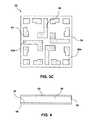
- FIGS. 3A-3Care side, top, and bottom views of an interposer according to the present invention.
- FIGS. 4-11are cross-sectional views illustrating methods for forming an interposer according to the present invention.
- FIG. 12is a cross-sectional view of a CSP embodiment wherein a semiconductor die is wire bonded to an interposer according to the present invention.
- FIGS. 13-16are cross-sectional views illustrating a method of forming the CSP of FIG. 12 .
- FIG. 17is a cross-sectional view of a CSP embodiment wherein a semiconductor die is flip-chip mounted to an interposer according to the present invention.
- FIGS. 18-20are cross-sectional views illustrating a method of forming the CSP of FIG. 17 .
- FIG. 21is a cross-sectional view of an MCM including an interposer according to the present invention.
- FIG. 22is a schematic diagram of a computer system incorporating an electronic device having an interposer according to the present invention.
- the present inventioncomprises an interposer for a semiconductor die package and materials and methods for forming such an interposer. While the following is described in terms of an interposer incorporated into a chip-scale package (CSP), it should be understood that the interposer may also be incorporated into other types of electronic device packages which are intended to be mounted to a carrier substrate.
- CSPchip-scale package
- interposer 26Central to interposer 26 is a substrate comprising a flexible core 28 formed of, for example, a conventional flexible circuit material such as a sheet of polyimide or a polyimide-based material.
- a flexible core 28formed of, for example, a conventional flexible circuit material such as a sheet of polyimide or a polyimide-based material.
- the term “flexible”means any material that allows at least one portion of flexible core 28 to be bent or positioned relative to another portion thereof without causing substantial damage to the elements of interposer 26 .
- a first side 30 of flexible core 28is formed with a plurality of discrete protrusions 32 extending in a substantially perpendicular direction outwardly therefrom, each tipped with a solder pad 34 .
- An opposing, second side 36 of flexible core 28is substantially planar and includes a conductive routing layer 38 .
- interposer 26further comprises conductive vias 40 extending through flexible core 28 from solder pads 34 to routing layer 38 .
- conductive vias 40extending through flexible core 28 from solder pads 34 to routing layer 38 .
- discrete protrusions 32 , the portions of vias 40 contained therein, and solder pads 34comprise flexible solder pad elements 42 .
- Both flexible solder pad elements 42 and routing layer 38may be used to attach interposer 26 to a carrier substrate or semiconductor die as described in further detail below.
- FIGS. 3B and 3Care, respectively, bottom and top views of interposer 26 showing the arrangement of flexible solder pad elements 42 and routing layer 38 .
- FIG. 3Bshows that flexible solder pad elements 42 are formed in an array pattern across first side 30 of flexible core 28 with discrete protrusions 32 topped by solder pads 34 overlying conductive vias 40 (not shown).
- routing layer 38 on second side 36 of flexible core 28is formed with a plurality of bond pads 44 in electrical communication with vias 40 (not shown in FIG. 3C ).
- Bond pads 44may be located directly above vias 40 in a pad-on-via configuration, as shown by bond pad 44 a, or may he displaced or offset to an alternate location, as shown by bond pad 44 b.
- solder pad elements 42 on first side 30 of flexible core 28may be rerouted into an alternate pattern for bond pads 44 on second side of flexible core 28 .
- arrangement of flexible solder pad elements 42 and routing layer 38 illustrated in FIGS. 3B and 3Cis only exemplary, as other patterns may be used depending on the desired location and number of solder pads 34 and bond pads 44 for interposer 26 .
- solder pads 34are depicted as having a circular shape and bond pads 44 are depicted as rectangular, any shape for either is possible within the scope of the present invention.
- flexible core 28is initially provided in the form of a substantially planar sheet of flexible circuit material having a first continuous layer of conductive material 46 overlying first side 30 and a second continuous layer of conductive material 48 overlying second side 36 .
- flexible core 28may be formed of polyimide or a polyimide-based material, commercially available examples of which include KAPTON® E polyimide film from DuPont High Performance Materials of Circleville, Ohio, APICAL® polyimide film from Kaneka High-Tech Materials, Inc. of Pasadena, Tex., and UPILEB®-S polyimide film from Ube Industries, Ltd. of Japan.
- the layers of conductive material 46 and 48may comprise, by way of example, sheets of a metal or metal alloy such as copper, which are laminated to flexible core 28 .
- FIG. 5shows that portions of the second layer of conductive material 48 are removed to form the pattern for routing layer 38 .
- Patterning of routing layer 38may be carried out using a conventional mask and etch process, wherein a photoresist (not shown) is applied over the layer of conductive material 48 and exposed to a source of radiant energy. Depending on the nature of the photoresist positive or negative), either the exposed or unexposed areas of the photoresist are then removed, and the uncovered portions of the underlying layer of conductive material 48 are subsequently removed by a chemical etchant.
- a suitable etching processmay comprise alkaline etching using ammonium hydroxide, Thereafter, the photoresist is stripped off, with the remaining portions of the layer of conductive material 48 providing routing layer 38 .
- FIG. 5shows that the portions of the layer of conductive material 48 overlying the locations where vias 40 (designated by broken lines) are to be formed are also removed in order to provide access to flexible core 28 through routing layer 38 .
- vias 40are then formed in flexible core 28 .
- FIG. 6shows that vias 40 pass through flexible core 28 and terminate at the first layer of conductive material 46 , which is left intact for the subsequent formation of solder pads 34 .
- One process that may be used to form vias 40 without removing the underlying layer of conductive material 46is by cutting through flexible core 28 with a beam of radiant energy, such as a laser. Based on the materials used for flexible core 28 and the layer of conductive material 46 , a laser wavelength may be selected that will be absorbed by and vaporize the portions of flexible core 28 in vias 40 while being substantially reflected by the layer of conductive material 46 , which is thereby left intact. In this manner, vias 40 may be formed with highly uniform and tightly controlled dimensions.
- vias 40may also be used, such as by way of a chemical etchant that selectively etches flexible core 28 without removing the underlying layer of conductive material 46 .
- the chemical etching processmay comprise a wet etch, where a fluid solution is applied to remove portions of flexible core 28 .
- flexible core 28comprises a polyimide, for example, a solution of potassium hydroxide (KOH) in an ethanol and water solvent would be suitable.
- the chemical etching processmay comprise a dry etch, using known reactive ion etching (RIE) methods.
- RIEreactive ion etching
- vias 40When the pitch is small, vias 40 will be closely spaced together and the high tolerances provided by individually forming each via 40 with a laser may be desirable. For larger pitches, chemical etching may be suitable and will enable vias 40 to be formed more rapidly than with a laser.
- FIGS. 7A-9Bshow exemplary processes for how vias 40 may be filled.
- a conductive liner 50 of a metal or metal alloy such as copperis formed onto the interior walls of vias 40 .
- Conductive liner 50comprises a seed layer deposited within vias 40 using a known electroless plating process, the thickness of which may be added to by a subsequent electroplating process once the seed layer has been formed.
- vias 40are completely plugged with a filler material 52 .
- filler material 52may comprise a conductive or nonconductive material that may be applied in a known fashion, for example, by stencil printing with a squeegee.
- suitable nonconductive materials for filling vias 40 by stencil printinginclude solder mask or epoxy plug materials hat are commercially available from vendors such as Taiyo America, Inc. of Carson City, Nev. (sold under the PSR product line).
- suitable conductive materialsinclude conductive pastes that are impregnated with copper, silver, lead, or other metal particles, commercially available examples of which include conductive copper paste (product no. AE3030) from Tatsuta Electric Wire & Cable Co. of Japan and silver via plugging material (product no. 1210) from Methode Development Co. of Chicago, Ill.
- FIGS. 9A and 9Bshow another exemplary process for filling vias 40 by using a conventional electroplating process.
- FIG. 9Ashows that electroplating material 54 in the form of a metal or metal alloy such as copper may be deposited within vias 40 by applying a voltage potential to the underlying layer of conductive material 46 and using the exposed portions of conductive material 46 within vias 40 to act as a cathode to attract electroplating material 54 .
- Additional electroplating material 54is deposited until vias 40 are filled up to the level of routing layer 38 as shown in FIG. 9B .
- FIG. 10shows that the layer of conductive material 46 may be patterned to form solder pads 34 .
- Solder pads 34may be formed by using a conventional mask and etch process to remove portions of the layer of conductive material 46 in the same manner as described above with respect to the patterning of routing layer 38 .
- a photoresist(not shown) is applied over the layer of conductive material 46 and exposed to a source of radiant energy projected with the desired pattern for solder pads 34 . The photoresist is then stripped off except for the areas overlying the selected locations for solder pads 34 , and the remaining uncovered portions of the layer of conductive material 46 are removed by an etching process, as previously discussed with relation to the formation of routing layer 38 .
- discrete protrusions 32are formed to complete interposer 26 .
- Discrete protrusions 32may be formed, by way of example, by applying an etchant to first side 30 of flexible core 28 that selectively etches the material forming flexible core 28 and does not remove the material forming solder pads 34 .
- the etching processmay comprise a wet etch, such as by applying a KOH solution as described above with respect to the formation of vias 40 , or may comprise a known dry etching process that uses plasma or laser energy to remove portions of flexible core 28 .
- solder pads 34act as a mask for the etching process, with the shape of solder pads 34 defining the resultant profile of discrete protrusions 32 .
- the etching processmay result in discrete protrusions 32 exhibiting a generally conical profile as depicted in FIG. 11 .
- Other profiles for discrete protrusions 32such as pyramids or columns, may be achieved by altering the shape of solder pads 34 and based on whether an isotropic or anisotropic etching process is used.
- the desired shape for discrete protrusions 32may depend on such factors as the required pitch for flexible solder pad elements 42 , the flexibility of the material used for flexible core 28 , and the layout of the circuitry to which solder pads 34 are to be connected.
- flexible solder pad elements 42may be formed without the inclusion of solder pads 34 .
- flexible core 28 illustrated in FIG. 4may be provided without the first layer of conductive material 46 , and vias 40 are then formed through flexible core 28 and plated or filled in the same manner as described with respect to FIGS. 7A-8 .
- flexible core 28may initially be provided with the first layer of conductive material 46 as shown in FIG. 4 and, after forming vias 40 , the first layer of conductive material may be completely removed by an etching process in the same manner as described with respect to FIG. 10 .
- discrete protrusions 32are formed as described above with respect to FIG. 11 , but with the ends of vias 40 exposed through flexible core 28 acting as a mask for the etching process.
- flexible solder pad elements 42are attached to a carrier substrate or semiconductor die by connection to the exposed ends of vias 40 on the tips of discrete protrusions 32 .
- interposer 26may be incorporated for use in electronic device packages such as CSPs.
- FIG. 12shows an embodiment of a CSP 56 wherein a semiconductor die 58 is electrically connected to interposer 26 using a wire bond interconnection method.
- semiconductor die 58is attached to second side 36 of interposer 26 such that solder pads 34 on flexible solder pad elements 42 are oriented for attachment to a carrier substrate 100 .
- CSP 56is attached to carrier substrate 100 by bonding solder pads 34 to corresponding solder pads 102 . Bonding may be effected in any conventional manner, for example, by using solder paste or a conductive or conductor filled adhesive to form a joint between solder pads 34 and solder pads 102 .
- flexible solder pad elements 42provide an interface between CSP 56 and carrier substrate 100 that overcomes the previously described problems associated with prior art LGA and BGA external electrode structures.
- the compliant nature of the material forming flexible core 28allows flexible solder pad elements 42 to absorb mismatches in expansion and contraction between carrier substrate 100 and the elements of CSP 56 without the occurrence of high internal stresses.
- flexible solder pad elements 42are also able to deform slightly in the vertical direction, thereby accommodating variations in distance between interposer 26 and carrier substrate 100 that may be caused by warped or uneven surfaces.
- flexible solder pad elementsare formed by etching the material of flexible core 28 , they do not require the additional processing involved with forming or attaching solder balls, and may be formed with pitches of 0.25 mm or below.
- FIGS. 13-16An exemplary method of forming CSP 56 is shown in FIGS. 13-16 .
- FIG. 13shows that a dielectric layer 60 is formed over second side 36 of interposer 26 in order to provide a semiconductor die mounting location that is electrically isolated from routing layer 38 .
- dielectric layer 60is sized to cover the central area of interposer 26 while leaving bond pads 44 of routing layer 38 exposed for subsequent wire bonding.
- Dielectric layer 60may be formed by deposition of a material such as one of the commercially available solder masks described above with respect to filler material 52 ; however, other materials may be used as long as they exhibit the desired dielectric isolation properties.
- FIG. 13shows that a dielectric layer 60 is formed over second side 36 of interposer 26 in order to provide a semiconductor die mounting location that is electrically isolated from routing layer 38 .
- dielectric layer 60is sized to cover the central area of interposer 26 while leaving bond pads 44 of routing layer 38 exposed for subsequent wire bonding.
- Dielectric layer 60may be formed by de
- FIG. 14shows that once dielectric layer 60 is formed, metal plating 62 such as sequential layers of nickel and gold may optionally be formed over bond pads 44 and solder pads 34 to improve wettability to solder, if desired or required. Application of metal plating 62 may be accomplished using an electrolytic or electroless plating process as known in the art.
- FIG. 15shows that semiconductor die 58 is mounted to dielectric layer 60 with a double-sided tape 64 coated with an adhesive on both sides such as KAPTON® tape, or other adhesive material, and wire bonds 66 are formed between bond pads 44 of routing layer 38 and bond pads 68 of semiconductor die 58 .
- FIG. 15shows that once dielectric layer 60 is formed, metal plating 62 such as sequential layers of nickel and gold may optionally be formed over bond pads 44 and solder pads 34 to improve wettability to solder, if desired or required. Application of metal plating 62 may be accomplished using an electrolytic or electroless plating process as known in the art.
- FIG. 15shows that semiconductor die 58 is mounted to dielectric layer
- FIG. 16shows an encapsulant 70 of, for example, a silicon-filled polymer-based molding compound applied using a conventional technique, such as transfer molding, over the second side 36 of interposer 26 to seal routing layer 38 , semiconductor die 58 , and wire bonds 66 from the surrounding environment.
- a conventional techniquesuch as transfer molding
- FIG. 17shows an embodiment of a CSP 72 wherein a semiconductor die 74 is electrically connected to interposer 26 using a flip-chip interconnection method.
- semiconductor die 74is attached to solder pads 34 on flexible solder pad elements 42 , and bond pads 44 of routing layer 38 are oriented for attachment to a carrier substrate 200 .
- CSP 74may be attached to carrier substrate 200 by bonding balls or bumps 76 formed on bond pads 44 to corresponding solder pads 202 .
- Balls or bumps 76may comprise solder or a conductive or conductor filled adhesive, and may be formed on or attached to bond pads 44 in any conventional manner.
- flexible solder pad elements 42provide an interface between semiconductor die 74 and interposer 26 .
- Such a configurationmay be desirable in situations where the coplanarity of semiconductor die 74 is an issue, or when stress caused by different expansion coefficients between semiconductor die 74 and interposer 26 is a concern.
- FIGS. 18-20An exemplary method of forming CSP 72 is shown in FIGS. 18-20 .
- metal plating 78such as sequential layers of nickel and gold, may be formed over bond pads 44 and solder pads 34 the same manner described with respect to CSP 56 if necessary or desirable to improve wettability.
- a solder mask 80 of the type described with respect to dielectric layer 60may also be applied to second side 36 of interposer 26 to protect and isolate routing layer 38 , with bond pads 44 being left exposed for subsequent attachment to carrier substrate 200 .
- semiconductor die 74is mounted to solder pads 34 by flip-chip attachment of semiconductor die bond pads 82 using a solder paste or other conductive or conductive filled adhesive material as known in the art.
- FIG. 18shows that metal plating 78 , such as sequential layers of nickel and gold, may be formed over bond pads 44 and solder pads 34 the same manner described with respect to CSP 56 if necessary or desirable to improve wettability.
- a solder mask 80 of the type described with respect to dielectric layer 60may also be
- underfill material 84may be accomplished, by way of example, using a conventional capillary-flow filling process.
- Underfill material 84may comprise any conventional nonconductive adhesive material.
- underfill material 84may comprise an anisotropic or “Z-axis” conductive material, in which case semiconductor die bond pads 82 may be electrically connected to solder pads 34 by underfill material 84 itself.
- an encapsulant 86such as the aforementioned polymer-based molding compound is then applied over the first side 30 of interposer 26 to seal flexible solder pad elements 42 and semiconductor die 74 from the surrounding environment, and balls or bumps 76 are formed on or attached to metal plating 78 and bond pads 44 .
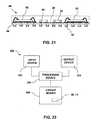
- FIG. 21shows one such electronic device package in the form of a multichip module (MCM) 88 .
- MCM 88includes an interposer 90 having a routing layer 38 and flexible solder pad elements 42 configured for electrically connecting multiple semiconductor dice 92 .
- FIG. 21also shows that electronic components 94 other than semiconductor dice, such as passive resistors, capacitors, or inductors, may also be included in MCM 88 by mounting to interposer 90 .
- FIG. 22depicted is a computer system 300 that includes an input device 302 and an output device 304 coupled to a processor device 306 , which, in turn, is coupled to a circuit board 308 incorporating at least one of the exemplary CSPs 56 and 72 , or various embodiments thereof, as illustrated in drawing FIGS. 12 and 17 .
- solder pads 34may be omitted and carrier substrate 100 or semiconductor die 74 may be directly bonded to exposed ends of vias 40 .
Landscapes
- Engineering & Computer Science (AREA)
- Microelectronics & Electronic Packaging (AREA)
- Power Engineering (AREA)
- Computer Hardware Design (AREA)
- Physics & Mathematics (AREA)
- General Physics & Mathematics (AREA)
- Theoretical Computer Science (AREA)
- Condensed Matter Physics & Semiconductors (AREA)
- Manufacturing & Machinery (AREA)
- General Engineering & Computer Science (AREA)
- Human Computer Interaction (AREA)
- Wire Bonding (AREA)
- Structures For Mounting Electric Components On Printed Circuit Boards (AREA)
Abstract
Description
- This application is a divisional of application Ser. No. 11/397,459, filed Apr. 4, 2006, pending, which is a divisional of Application Ser. No. 10/923,588, filed Aug. 19, 2004, now U.S. Pat. No. 7,105,918, issued Sep. 12, 2006. The disclosures of the previously referenced U.S. patent application and patent are hereby incorporated by reference in their entirety.
- 1. Field of the Invention
- The present invention relates generally to packaging of electronic devices in the form of semiconductor dice. More particularly, the present invention relates to embodiments of an interposer for mounting a semiconductor die, wherein the interposer includes flexible solder pad elements configured for attachment to a carrier substrate or to the semiconductor die. The present invention further relates to materials and methods for forming the interposer.
- 2. State of the Art
- An electronic device in the form of a semiconductor die or chip is conventionally manufactured of materials such as silicon, germanium, or gallium arsenide. Circuitry is formed on an active surface of the semiconductor die and may include further levels of circuitry within the die itself. Due to the materials used and the intricate nature of construction, semiconductor dice are highly susceptible to physical damage or contamination from environmental conditions including, for example, moisture. In order to protect a semiconductor die from environmental conditions, it is commonly enclosed within a package that provides hermetic sealing and prevents environmental elements from physically contacting the semiconductor die.
- In recent years, the demand for more compact electronic devices has increased, and this trend has led to the development of so called “chip-scale packages” (CSPs). One exemplary CSP design is typified by mounting a semiconductor die to a substrate, termed an interposer, having substantially the same dimensions as the semiconductor die. Bond pads of the semiconductor die are electrically connected to bond pads on a first surface of the interposer, and the semiconductor die is encased within an encapsulant material. Conductive pathways, which may comprise a combination of traces and vias, extend from the interposer bond pads to a second, opposing side of the interposer where they terminate in external electrodes to which further electrical connections are made. Typically, a CSP is then mounted to a carrier substrate, such as a circuit board having a number of other electronic devices attached thereto.
- Electrically connecting the bond pads of a semiconductor die to the bond pads of a CSP interposer generally involves using one of two types of interconnection methods, depending on the manner in which the semiconductor die is mounted. As shown by
FIG. 1 , aCSP 2 is configured with the first interconnection method by mounting a semiconductor die4 to aninterposer 6 withdie bond pads 8 in a face-up orientation, and electrically connectingdie bonds pads 8 to interposerbond pads 10 withbond wires 12. As shown byFIG. 2 ,CSP 2′ is configured with the second interconnection method by mounting semiconductor die4 withdie bond pads 8 in a face-down or flip-chip orientation, and electrically connectingdie bond pads 8 directly tointerposer bond pads 10 with conductive elements, such asbumps 14, formed of solder or a conductive adhesive material. Once the interconnection method used forCSP 2 orCSP 2′ is complete, semiconductor die4 is encased within anencapsulant material 15 such as a polymer-based molding compound. - Further,
FIGS. 1 and 2 show there are generally two types of external electrode structures used for mounting CSPs to acarrier substrate 16.CSP 2 ofFIG. 1 is configured as a land grid array (LGA) type package, wherein the external electrodes comprisesolder pads 18 that are intended to be directly attached tocorresponding solder pads 20 on acarrier substrate 16. InFIG. 2 ,CSP 2′ is configured as a ball grid array (BGA) type package, wherein the external electrodes comprisesolder ball pads 22 havingsolder balls 24 formed thereon, such thatsolder balls 24 will be attached to thesolder pads 20 oncarrier substrate 16. - Although CSPs of the type described above have provided a compact and economical approach to packaging of semiconductor dice, they still present certain disadvantages, especially in terms of the LGA or BGA electrode structures used for mounting CSPs to a caner substrate.
- During the operation of an electronic device configured as a CSP, for example, the functioning of the circuits within the semiconductor die and resistance in the circuit connections of the semiconductor die, interposer, and carrier substrate generate heat. This heating results in the expansion and contraction of all of these components as temperatures rise and fall. Because the semiconductor die, interposer, and carrier substrate are made of different materials exhibiting different coefficients of thermal expansion (CTE), they expand and contract at different rates during thermal cycling. This mismatch in thermal expansion rates places stress on the electrode structures joining the CSP interposer to the carrier substrate, and may eventually cause cracks in the electrode structures leading to the failure of electrical connections.
- This thermal stress may be especially problematic with a CSP configured as an LGA type package as in
FIG. 1 , because the stress is concentrated within the relatively small thickness H of thesolder pads 18 betweeninterposer 6 andcarrier substrate 16. With a CSP configured as a BGA type package as inFIG. 2 , the thermal stress may be more effectively absorbed by being spread across the increased thickness H′ provided by thesolder balls 24. However, because modern circuitry layouts tend to require increasing numbers of I/Os, the external electrodes on a CSP must be very densely spaced, and there are physical limits to the minimum spacing that may be attained when formingsolder balls 24. The conventional process of printing and reflowing solder paste onsolder ball pads 22 to formsolder balls 24, for example, requires thatsolder ball pads 22 must be spaced at a pitch of about 0.4 mm to ensure reliable formation without bridging. Furthermore, high I/O CSPs require the use of smaller diameter solder balls that may not provide a thickness H′ sufficient to overcome thermal induced stress failures. Forming a CSP as a BGA type package also includes the additional processing required to formsolder balls 24, which is undesirable in terms of mass-scale production. - Another problem associated with prior art package interposers is that the LGA or BGA type external electrode structures are typically formed entirely of metal or metal alloys and are, therefore, rigid. In many cases, one or both of the interposer and the carrier substrate to which it is to be mounted may have uneven surfaces or may become warped by thermal stresses during attachment of a CSP by solder reflow. When his occurs, the space between the interposer and the carrier substrate may vary, and the rigid construction of LGA or BGA type external electrodes in contact with the carrier substrate at narrower spaces may prevent contact by external electrodes at wider spaces.
- In view of the foregoing, what is needed is an interposer for a semiconductor die package such as a CSP that is simple and inexpensive to produce and overcomes the problems associated with the prior art external electrode structures used to mount the interposer to a carrier substrate.
- In accordance with the present invention, an improved interposer for electronic device packages is disclosed, as well as electronic device packages including such an interposer. The interposer is formed with flexible solder pad elements that overcome the drawbacks associated with prior art external electrode structures. Due to its flexible nature, the interposer of the present invention is more readily able to accommodate thermal induced stresses and is more easily conformed to carrier substrate or semiconductor die surfaces that are warped or uneven. Furthermore, by forming the flexible solder pad elements as a unitary part of core material of the interposer, the interposer manufacturing process is simplified over prior art interposer methods that require additional processing to form or attach conventional external electrode structures.
- In one embodiment of the present invention, the interposer comprises a substrate having a first side and an opposing, second side and comprising a flexible core material; at least one flexible solder pad element on the second side of the substrate, wherein the at least one flexible solder pad element comprises a discrete protrusion of the flexible core material extending in a substantially perpendicular direction outwardly from the first side of the substrate and a solder pad on a tip of the protrusion; a conductive via extending from the solder pad of the at least one flexible solder pad element to the second side of the substrate; and a conductive routing layer on the second side of the substrate having at least one bond pad electrically connected to the solder pad of the at least one flexible solder pad element by the conductive via.
- In further embodiments of the present invention, the interposer is incorporated into an electronic device package having at least one semiconductor die mounted to and electrically connected to the interposer. According to one embodiment of an electronic device package, the at least one semiconductor die is electrically connected to the interposer by at least one wire bond extending between at least one bond pad of the at least one semiconductor die and the at least one bond pad of the conductive routing layer of the interposer. Under this package embodiment, the at least one flexible solder pad element of the interposer may be attached to a carrier substrate such as a computer circuit board of a computer system. According to another embodiment of an electronic device package, the at least one semiconductor die is electrically connected to the interposer in a flip-chip configuration by a bond between at least one bond pad of the semiconductor die and the at least one bond pad of the interposer. Under this package embodiment, the at least one bond pad of the conductive routing layer of the interposer is attached to a carrier substrate. In another embodiment of the present invention, a plurality of semiconductor devices is mounted to, and electrically connected to, the interposer.
- The present invention also discloses methods for forming the interposer and the electronic device packages including the interposer. According to one method, the interposer is formed by providing a substrate comprising a flexible core material having a first side with a first layer of conductive material and a second side with a second layer of conductive material; patterning the second layer of conductive material to form a conductive routing layer having at least one bond pad; forming at least one conductive via extending through the flexible core material between the conductive routing layer and the first layer of conductive material; patterning the first layer of conductive material to form at least one solder pad overlying the at least one conductive via; and removing portions of the flexible core material from the first side of the substrate around the at least one solder pad to form at least one flexible solder pad element comprising a discrete protrusion of the flexible core material extending in a substantially perpendicular direction outwardly from the first side of the substrate.
- According to further methods of the present invention, electronic device packages are formed by mounting and electrically connecting at least one semiconductor die to the interposer. According to one method of forming an electronic device package, electrically connecting the at least one semiconductor die to the interposer comprises attaching a wire bond between at least one bond pad of the at least one semiconductor die and the at least one bond pad of the conductive routing layer of the interposer. According to another method of forming an electronic device package, electrically connecting the at least one semiconductor die to the interposer comprises bonding at least one bond pad of the semiconductor die to the at least one bond pad of the interposer in a flip-chip configuration.
- Other and further features and advantages will be apparent from the following detailed description of the invention taken in conjunction with the accompanying drawings. The following examples are provided for the purposes of illustration only, and are not intended to be limiting. It will be understood by one of ordinary skill in the art that numerous combinations and modifications are possible for the embodiments presented herein.
- In the drawings, which illustrate what is currently considered to be the best mode for carrying out the invention:
FIG. 1 is a cross-sectional side view of a prior art CSP having wire bond interconnections and LGA type external electrodes.- FIG;2 is cross-sectional side view of a prior art CSP having flip-chip interconnections and BGA type external electrodes.
FIGS. 3A-3C are side, top, and bottom views of an interposer according to the present invention.FIGS. 4-11 are cross-sectional views illustrating methods for forming an interposer according to the present invention.FIG. 12 is a cross-sectional view of a CSP embodiment wherein a semiconductor die is wire bonded to an interposer according to the present invention.FIGS. 13-16 are cross-sectional views illustrating a method of forming the CSP ofFIG. 12 .FIG. 17 is a cross-sectional view of a CSP embodiment wherein a semiconductor die is flip-chip mounted to an interposer according to the present invention.FIGS. 18-20 are cross-sectional views illustrating a method of forming the CSP ofFIG. 17 .FIG. 21 is a cross-sectional view of an MCM including an interposer according to the present invention.FIG. 22 is a schematic diagram of a computer system incorporating an electronic device having an interposer according to the present invention.- As described in further detail below, the present invention comprises an interposer for a semiconductor die package and materials and methods for forming such an interposer. While the following is described in terms of an interposer incorporated into a chip-scale package (CSP), it should be understood that the interposer may also be incorporated into other types of electronic device packages which are intended to be mounted to a carrier substrate.
- Embodiments of the present invention are described with reference to the accompanying drawings, which illustrate exemplary interposer and CSP structures and methods for their formation. To simplify the description of the present invention, common elements of the various embodiments illustrated by the drawings are designated with like reference numerals. It should be understood that the drawings are not illustrative of actual views of any particular portion of the actual embodiment structures, but are merely idealized schematic representations which are employed to more clearly and fully depict the invention.
- Turning to
FIGS. 3A-3C , the general structure of anexemplary interposer 26 according to the present invention is illustrated. Central to interposer26 is a substrate comprising aflexible core 28 formed of, for example, a conventional flexible circuit material such as a sheet of polyimide or a polyimide-based material. As used herein, the term “flexible” means any material that allows at least one portion offlexible core 28 to be bent or positioned relative to another portion thereof without causing substantial damage to the elements ofinterposer 26. Afirst side 30 offlexible core 28 is formed with a plurality ofdiscrete protrusions 32 extending in a substantially perpendicular direction outwardly therefrom, each tipped with asolder pad 34. An opposing,second side 36 offlexible core 28 is substantially planar and includes aconductive routing layer 38. As seen inFIG. 3A ,interposer 26 further comprisesconductive vias 40 extending throughflexible core 28 fromsolder pads 34 torouting layer 38. Together,discrete protrusions 32, the portions ofvias 40 contained therein, andsolder pads 34 comprise flexiblesolder pad elements 42. Both flexiblesolder pad elements 42 androuting layer 38 may be used to attachinterposer 26 to a carrier substrate or semiconductor die as described in further detail below. FIGS. 3B and 3C are, respectively, bottom and top views ofinterposer 26 showing the arrangement of flexiblesolder pad elements 42 androuting layer 38.FIG. 3B shows that flexiblesolder pad elements 42 are formed in an array pattern acrossfirst side 30 offlexible core 28 withdiscrete protrusions 32 topped bysolder pads 34 overlying conductive vias40 (not shown). As seen inFIG. 3C ,routing layer 38 onsecond side 36 offlexible core 28 is formed with a plurality ofbond pads 44 in electrical communication with vias40 (not shown inFIG. 3C ).Bond pads 44 may be located directly abovevias 40 in a pad-on-via configuration, as shown bybond pad 44a,or may he displaced or offset to an alternate location, as shown bybond pad 44b.In this manner the array pattern of flexiblesolder pad elements 42 onfirst side 30 offlexible core 28 may be rerouted into an alternate pattern forbond pads 44 on second side offlexible core 28. It should be understood that the arrangement of flexiblesolder pad elements 42 androuting layer 38 illustrated inFIGS. 3B and 3C is only exemplary, as other patterns may be used depending on the desired location and number ofsolder pads 34 andbond pads 44 forinterposer 26. Likewise, whilesolder pads 34 are depicted as having a circular shape andbond pads 44 are depicted as rectangular, any shape for either is possible within the scope of the present invention.- Exemplary methods of
manufacturing interposer 26 will now be described with reference toFIGS. 4-11 . As seen inFIG. 4 ,flexible core 28 is initially provided in the form of a substantially planar sheet of flexible circuit material having a first continuous layer ofconductive material 46 overlyingfirst side 30 and a second continuous layer ofconductive material 48 overlyingsecond side 36. As previously discussed above,flexible core 28 may be formed of polyimide or a polyimide-based material, commercially available examples of which include KAPTON® E polyimide film from DuPont High Performance Materials of Circleville, Ohio, APICAL® polyimide film from Kaneka High-Tech Materials, Inc. of Pasadena, Tex., and UPILEB®-S polyimide film from Ube Industries, Ltd. of Japan. The layers ofconductive material flexible core 28. FIG. 5 shows that portions of the second layer ofconductive material 48 are removed to form the pattern for routinglayer 38. Patterning ofrouting layer 38 may be carried out using a conventional mask and etch process, wherein a photoresist (not shown) is applied over the layer ofconductive material 48 and exposed to a source of radiant energy. Depending on the nature of the photoresist positive or negative), either the exposed or unexposed areas of the photoresist are then removed, and the uncovered portions of the underlying layer ofconductive material 48 are subsequently removed by a chemical etchant. If the layer of conductive material comprises copper, for example, a suitable etching process may comprise alkaline etching using ammonium hydroxide, Thereafter, the photoresist is stripped off, with the remaining portions of the layer ofconductive material 48 providingrouting layer 38. When routinglayer 38 is patterned,FIG. 5 shows that the portions of the layer ofconductive material 48 overlying the locations where vias40 (designated by broken lines) are to be formed are also removed in order to provide access toflexible core 28 throughrouting layer 38.- As seen in
FIG. 6 , vias40 are then formed inflexible core 28.FIG. 6 shows that vias40 pass throughflexible core 28 and terminate at the first layer ofconductive material 46, which is left intact for the subsequent formation ofsolder pads 34. One process that may be used to formvias 40 without removing the underlying layer ofconductive material 46 is by cutting throughflexible core 28 with a beam of radiant energy, such as a laser. Based on the materials used forflexible core 28 and the layer ofconductive material 46, a laser wavelength may be selected that will be absorbed by and vaporize the portions offlexible core 28 invias 40 while being substantially reflected by the layer ofconductive material 46, which is thereby left intact. In this manner, vias40 may be formed with highly uniform and tightly controlled dimensions. Other known processes for formingvias 40 may also be used, such as by way of a chemical etchant that selectively etchesflexible core 28 without removing the underlying layer ofconductive material 46. The chemical etching process may comprise a wet etch, where a fluid solution is applied to remove portions offlexible core 28. Ifflexible core 28 comprises a polyimide, for example, a solution of potassium hydroxide (KOH) in an ethanol and water solvent would be suitable. Alternatively, the chemical etching process may comprise a dry etch, using known reactive ion etching (RIE) methods. The process used for formingvias 40 may depend, in part, on the desired pitch of flexiblesolder pad elements 42 oninterposer 26. When the pitch is small, vias40 will be closely spaced together and the high tolerances provided by individually forming each via40 with a laser may be desirable. For larger pitches, chemical etching may be suitable and will enablevias 40 to be formed more rapidly than with a laser. - Once
vias 40 have been cut throughflexible core 28, they are filled to provide conductive pathways betweenrouting layer 38 and the portions of the layer ofconductive material 46 that will be formed intosolder pads 34.FIGS. 7A-9B show exemplary processes for how vias40 may be filled. In a first process shown inFIG. 7A-7B , aconductive liner 50 of a metal or metal alloy such as copper is formed onto the interior walls ofvias 40.Conductive liner 50 comprises a seed layer deposited withinvias 40 using a known electroless plating process, the thickness of which may be added to by a subsequent electroplating process once the seed layer has been formed. Thereafter, as seen inFIG. 7B , vias40 are completely plugged with afiller material 52. - Depending on the desired characteristics for
vias 40,filler material 52 may comprise a conductive or nonconductive material that may be applied in a known fashion, for example, by stencil printing with a squeegee. Examples of suitable nonconductive materials for fillingvias 40 by stencil printing include solder mask or epoxy plug materials hat are commercially available from vendors such as Taiyo America, Inc. of Carson City, Nev. (sold under the PSR product line). Examples of suitable conductive materials include conductive pastes that are impregnated with copper, silver, lead, or other metal particles, commercially available examples of which include conductive copper paste (product no. AE3030) from Tatsuta Electric Wire & Cable Co. of Japan and silver via plugging material (product no. 1210) from Methode Development Co. of Chicago, Ill. - When filling
vias 40 with the above-described conductive materials, it is also contemplated that the formation ofconductive liner 50 may be omitted. Instead, aconductive filler material 52 may simply be applied by stencil printing to entirely fill the interiors ofvias 40, as shown inFIG. 8 .FIGS. 9A and 9B show another exemplary process for fillingvias 40 by using a conventional electroplating process. Using this approach,FIG. 9A shows that electroplatingmaterial 54 in the form of a metal or metal alloy such as copper may be deposited withinvias 40 by applying a voltage potential to the underlying layer ofconductive material 46 and using the exposed portions ofconductive material 46 withinvias 40 to act as a cathode to attractelectroplating material 54.Additional electroplating material 54 is deposited untilvias 40 are filled up to the level ofrouting layer 38 as shown inFIG. 9B . - After vias40 have been filled,
FIG. 10 shows that the layer ofconductive material 46 may be patterned to formsolder pads 34.Solder pads 34 may be formed by using a conventional mask and etch process to remove portions of the layer ofconductive material 46 in the same manner as described above with respect to the patterning ofrouting layer 38. A photoresist (not shown) is applied over the layer ofconductive material 46 and exposed to a source of radiant energy projected with the desired pattern forsolder pads 34. The photoresist is then stripped off except for the areas overlying the selected locations forsolder pads 34, and the remaining uncovered portions of the layer ofconductive material 46 are removed by an etching process, as previously discussed with relation to the formation ofrouting layer 38. - Finally, as seen in
FIG. 11 ,discrete protrusions 32 are formed to completeinterposer 26.Discrete protrusions 32 may be formed, by way of example, by applying an etchant tofirst side 30 offlexible core 28 that selectively etches the material formingflexible core 28 and does not remove the material formingsolder pads 34. The etching process may comprise a wet etch, such as by applying a KOH solution as described above with respect to the formation ofvias 40, or may comprise a known dry etching process that uses plasma or laser energy to remove portions offlexible core 28. In this manner,solder pads 34 act as a mask for the etching process, with the shape ofsolder pads 34 defining the resultant profile ofdiscrete protrusions 32. With circular shapedsolder pads 34, for example, the etching process may result indiscrete protrusions 32 exhibiting a generally conical profile as depicted inFIG. 11 . Other profiles fordiscrete protrusions 32, such as pyramids or columns, may be achieved by altering the shape ofsolder pads 34 and based on whether an isotropic or anisotropic etching process is used. The desired shape fordiscrete protrusions 32 may depend on such factors as the required pitch for flexiblesolder pad elements 42, the flexibility of the material used forflexible core 28, and the layout of the circuitry to whichsolder pads 34 are to be connected. - As an alternative to the above-described structure of
interposer 26, it is also contemplated within the scope of the present invention that flexiblesolder pad elements 42 may be formed without the inclusion ofsolder pads 34. Under this embodiment,flexible core 28 illustrated inFIG. 4 may be provided without the first layer ofconductive material 46, and vias40 are then formed throughflexible core 28 and plated or filled in the same manner as described with respect toFIGS. 7A-8 . Alternatively,flexible core 28 may initially be provided with the first layer ofconductive material 46 as shown inFIG. 4 and, after formingvias 40, the first layer of conductive material may be completely removed by an etching process in the same manner as described with respect toFIG. 10 . Thereafter,discrete protrusions 32 are formed as described above with respect toFIG. 11 , but with the ends ofvias 40 exposed throughflexible core 28 acting as a mask for the etching process. With the structure ofinterposer 26 whereinsolder pads 34 have been omitted, flexiblesolder pad elements 42 are attached to a carrier substrate or semiconductor die by connection to the exposed ends ofvias 40 on the tips ofdiscrete protrusions 32. - Having described the basic structure of
interposer 26 and methods for its formation, it will now be shown howinterposer 26 may be incorporated for use in electronic device packages such as CSPs. FIG. 12 shows an embodiment of aCSP 56 wherein asemiconductor die 58 is electrically connected to interposer26 using a wire bond interconnection method. According to this embodiment, semiconductor die58 is attached tosecond side 36 ofinterposer 26 such thatsolder pads 34 on flexiblesolder pad elements 42 are oriented for attachment to acarrier substrate 100.CSP 56 is attached tocarrier substrate 100 by bondingsolder pads 34 tocorresponding solder pads 102. Bonding may be effected in any conventional manner, for example, by using solder paste or a conductive or conductor filled adhesive to form a joint betweensolder pads 34 andsolder pads 102.- With this package configuration, flexible
solder pad elements 42 provide an interface betweenCSP 56 andcarrier substrate 100 that overcomes the previously described problems associated with prior art LGA and BGA external electrode structures. The compliant nature of the material formingflexible core 28, for example, allows flexiblesolder pad elements 42 to absorb mismatches in expansion and contraction betweencarrier substrate 100 and the elements ofCSP 56 without the occurrence of high internal stresses. Unlike the rigid LGA and BGA electrode structures, flexiblesolder pad elements 42 are also able to deform slightly in the vertical direction, thereby accommodating variations in distance betweeninterposer 26 andcarrier substrate 100 that may be caused by warped or uneven surfaces. Furthermore, because flexible solder pad elements are formed by etching the material offlexible core 28, they do not require the additional processing involved with forming or attaching solder balls, and may be formed with pitches of 0.25 mm or below. - An exemplary method of forming
CSP 56 is shown inFIGS. 13-16 . First,FIG. 13 shows that adielectric layer 60 is formed oversecond side 36 ofinterposer 26 in order to provide a semiconductor die mounting location that is electrically isolated from routinglayer 38. As illustrated inFIG. 13 ,dielectric layer 60 is sized to cover the central area ofinterposer 26 while leavingbond pads 44 ofrouting layer 38 exposed for subsequent wire bonding.Dielectric layer 60 may be formed by deposition of a material such as one of the commercially available solder masks described above with respect tofiller material 52; however, other materials may be used as long as they exhibit the desired dielectric isolation properties.FIG. 14 shows that oncedielectric layer 60 is formed, metal plating62 such as sequential layers of nickel and gold may optionally be formed overbond pads 44 andsolder pads 34 to improve wettability to solder, if desired or required. Application of metal plating62 may be accomplished using an electrolytic or electroless plating process as known in the art. Thereafter,FIG. 15 shows that semiconductor die58 is mounted todielectric layer 60 with a double-sided tape 64 coated with an adhesive on both sides such as KAPTON® tape, or other adhesive material, andwire bonds 66 are formed betweenbond pads 44 ofrouting layer 38 andbond pads 68 of semiconductor die58. To completeCSP 56,FIG. 16 shows anencapsulant 70 of, for example, a silicon-filled polymer-based molding compound applied using a conventional technique, such as transfer molding, over thesecond side 36 ofinterposer 26 to sealrouting layer 38, semiconductor die58, andwire bonds 66 from the surrounding environment. FIG. 17 shows an embodiment of aCSP 72 wherein asemiconductor die 74 is electrically connected to interposer26 using a flip-chip interconnection method. According to this embodiment, semiconductor die74 is attached tosolder pads 34 on flexiblesolder pad elements 42, andbond pads 44 ofrouting layer 38 are oriented for attachment to acarrier substrate 200. As seen inFIG. 17 ,CSP 74 may be attached tocarrier substrate 200 by bonding balls or bumps76 formed onbond pads 44 tocorresponding solder pads 202. Balls or bumps76 may comprise solder or a conductive or conductor filled adhesive, and may be formed on or attached tobond pads 44 in any conventional manner. Using this package configuration, flexiblesolder pad elements 42 provide an interface between semiconductor die74 andinterposer 26. Such a configuration may be desirable in situations where the coplanarity of semiconductor die74 is an issue, or when stress caused by different expansion coefficients between semiconductor die74 andinterposer 26 is a concern.- An exemplary method of forming
CSP 72 is shown inFIGS. 18-20 . First,FIG. 18 shows that metal plating78, such as sequential layers of nickel and gold, may be formed overbond pads 44 andsolder pads 34 the same manner described with respect toCSP 56 if necessary or desirable to improve wettability. Asolder mask 80 of the type described with respect todielectric layer 60 may also be applied tosecond side 36 ofinterposer 26 to protect and isolaterouting layer 38, withbond pads 44 being left exposed for subsequent attachment tocarrier substrate 200. Thereafter, inFIG. 19 , semiconductor die74 is mounted tosolder pads 34 by flip-chip attachment of semiconductor diebond pads 82 using a solder paste or other conductive or conductive filled adhesive material as known in the art.FIG. 19 shows that the spaces between semiconductor die74 and flexiblesolder pad elements 42 may optionally be filled with anunderfill material 84 to seal the underside of semiconductor die74 and reinforce the attachment withinterposer 26. Application ofunderfill material 84 may be accomplished, by way of example, using a conventional capillary-flow filling process.Underfill material 84 may comprise any conventional nonconductive adhesive material. Alternatively,underfill material 84 may comprise an anisotropic or “Z-axis” conductive material, in which case semiconductor diebond pads 82 may be electrically connected tosolder pads 34 byunderfill material 84 itself. Once semiconductor die74 has been mounted,FIG. 20 shows that anencapsulant 86 such as the aforementioned polymer-based molding compound is then applied over thefirst side 30 ofinterposer 26 to seal flexiblesolder pad elements 42 and semiconductor die74 from the surrounding environment, and balls or bumps76 are formed on or attached to metal plating78 andbond pads 44. - While described in terms of being formed for incorporation into
individual CSPs FIG. 21 shows one such electronic device package in the form of a multichip module (MCM)88. As seen inFIG. 21 ,MCM 88 includes aninterposer 90 having arouting layer 38 and flexiblesolder pad elements 42 configured for electrically connectingmultiple semiconductor dice 92.FIG. 21 also shows thatelectronic components 94 other than semiconductor dice, such as passive resistors, capacitors, or inductors, may also be included inMCM 88 by mounting tointerposer 90. - Referring to
FIG. 22 , depicted is acomputer system 300 that includes aninput device 302 and anoutput device 304 coupled to aprocessor device 306, which, in turn, is coupled to acircuit board 308 incorporating at least one of theexemplary CSPs FIGS. 12 and 17 . - Although the present invention has been described with respect to the illustrated embodiments, various additions, deletions and modifications are contemplated as being within its scope. For instance, other materials aside from the above-described polyimide films may be used for
flexible core 28 within the scope of the present invention, as long as they exhibit the desired flexibility and have the capability to be etched or otherwise shaped to include flexiblesolder pad elements 42. Likewise, whileinterposer 26 has been illustrated as being configured for forming a single CSP, it is possible that an interposer according to the present invention could be configured to receive multiple semiconductor dice and then singulated for simultaneous formation of multiple CSPs. Furthermore, whileFIGS. 12 and 17 illustrateCSPs interposer 26 is attached to acarrier substrate 100 or semiconductor die74 by way ofsolder pads 34, as described above,solder pads 34 may be omitted andcarrier substrate 100 or semiconductor die74 may be directly bonded to exposed ends ofvias 40. The scope of the invention is, therefore, indicated by the appended claims rather than the foregoing description. Further, all changes which may fall within the meaning and range of equivalency of the claims and elements and features thereof are to be embraced within their scope,
Claims (1)
Priority Applications (1)
| Application Number | Priority Date | Filing Date | Title |
|---|---|---|---|
| US11/841,351US9412677B2 (en) | 2004-07-29 | 2007-08-20 | Computer systems having an interposer including a flexible material |
Applications Claiming Priority (6)
| Application Number | Priority Date | Filing Date | Title |
|---|---|---|---|
| SG2004043501ASG119238A1 (en) | 2004-07-29 | 2004-07-29 | Interposer with flexible solder pad elements and methods of manufacturing the same |
| SG200404350 | 2004-07-29 | ||
| SG200404350-1 | 2004-07-29 | ||
| US10/923,588US7105918B2 (en) | 2004-07-29 | 2004-08-19 | Interposer with flexible solder pad elements and methods of manufacturing the same |
| US11/397,459US7397129B2 (en) | 2004-07-29 | 2006-04-04 | Interposers with flexible solder pad elements |
| US11/841,351US9412677B2 (en) | 2004-07-29 | 2007-08-20 | Computer systems having an interposer including a flexible material |
Related Parent Applications (1)
| Application Number | Title | Priority Date | Filing Date |
|---|---|---|---|
| US11/397,459DivisionUS7397129B2 (en) | 2004-07-29 | 2006-04-04 | Interposers with flexible solder pad elements |
Publications (2)
| Publication Number | Publication Date |
|---|---|
| US20070285884A1true US20070285884A1 (en) | 2007-12-13 |
| US9412677B2 US9412677B2 (en) | 2016-08-09 |
Family
ID=56555123
Family Applications (4)
| Application Number | Title | Priority Date | Filing Date |
|---|---|---|---|
| US10/923,588Expired - Fee RelatedUS7105918B2 (en) | 2004-07-29 | 2004-08-19 | Interposer with flexible solder pad elements and methods of manufacturing the same |
| US11/301,807Expired - LifetimeUS7422978B2 (en) | 2004-07-29 | 2005-12-13 | Methods of manufacturing interposers with flexible solder pad elements |
| US11/397,459Expired - LifetimeUS7397129B2 (en) | 2004-07-29 | 2006-04-04 | Interposers with flexible solder pad elements |
| US11/841,351Active2027-07-01US9412677B2 (en) | 2004-07-29 | 2007-08-20 | Computer systems having an interposer including a flexible material |
Family Applications Before (3)
| Application Number | Title | Priority Date | Filing Date |
|---|---|---|---|
| US10/923,588Expired - Fee RelatedUS7105918B2 (en) | 2004-07-29 | 2004-08-19 | Interposer with flexible solder pad elements and methods of manufacturing the same |
| US11/301,807Expired - LifetimeUS7422978B2 (en) | 2004-07-29 | 2005-12-13 | Methods of manufacturing interposers with flexible solder pad elements |
| US11/397,459Expired - LifetimeUS7397129B2 (en) | 2004-07-29 | 2006-04-04 | Interposers with flexible solder pad elements |
Country Status (1)
| Country | Link |
|---|---|
| US (4) | US7105918B2 (en) |
Cited By (5)
| Publication number | Priority date | Publication date | Assignee | Title |
|---|---|---|---|---|
| US20080020601A1 (en)* | 2005-09-08 | 2008-01-24 | International Business Machines Corporation | Land grid array (lga) interposer utilizing metal-on-elastomer hemi-torus and other multiple points of contact geometries |
| US20110085314A1 (en)* | 2007-08-16 | 2011-04-14 | Michael Franz | Electrical circuit system and method for producing an electrical circuit system |
| US20150201497A1 (en)* | 2009-12-16 | 2015-07-16 | Intel Corporation | High-density inter-package connections for ultra-thin package-on-package structures, and processes of forming same |
| EP3432024A1 (en)* | 2017-07-18 | 2019-01-23 | Samsung Electronics Co., Ltd. | Bonding interposer and integrated circuit chip, and ultrasound probe using the same |
| KR20190009162A (en)* | 2017-07-18 | 2019-01-28 | 삼성전자주식회사 | Interposer, ultrasonic probe using the same, and method of manufacturing the interposer |
Families Citing this family (43)
| Publication number | Priority date | Publication date | Assignee | Title |
|---|---|---|---|---|
| US8330270B1 (en)* | 1998-06-10 | 2012-12-11 | Utac Hong Kong Limited | Integrated circuit package having a plurality of spaced apart pad portions |
| FR2861216B1 (en)* | 2003-10-21 | 2006-02-10 | St Microelectronics Sa | SEMICONDUCTOR PACKAGE WITH CHIP ON SUPPORT PLATE |
| JP2005340647A (en)* | 2004-05-28 | 2005-12-08 | Nec Compound Semiconductor Devices Ltd | Interposer substrate, semiconductor package, semiconductor device, and method for manufacturing them |
| US7290332B1 (en)* | 2004-08-31 | 2007-11-06 | Exatron, Inc. | Method of constructing an interposer |
| DE102004046227B3 (en)* | 2004-09-22 | 2006-04-20 | Infineon Technologies Ag | Method for producing a semiconductor component with through contacts through a plastic housing composition and corresponding semiconductor component |
| US7332801B2 (en)* | 2004-09-30 | 2008-02-19 | Intel Corporation | Electronic device |
| US7371676B2 (en)* | 2005-04-08 | 2008-05-13 | Micron Technology, Inc. | Method for fabricating semiconductor components with through wire interconnects |
| US7393770B2 (en)* | 2005-05-19 | 2008-07-01 | Micron Technology, Inc. | Backside method for fabricating semiconductor components with conductive interconnects |
| US8399291B2 (en)* | 2005-06-29 | 2013-03-19 | Intel Corporation | Underfill device and method |
| US7307348B2 (en)* | 2005-12-07 | 2007-12-11 | Micron Technology, Inc. | Semiconductor components having through wire interconnects (TWI) |
| TWI294677B (en)* | 2006-03-31 | 2008-03-11 | Ind Tech Res Inst | Interconnect structure with stress buffering ability and the manufacturing method thereof |
| US7659612B2 (en) | 2006-04-24 | 2010-02-09 | Micron Technology, Inc. | Semiconductor components having encapsulated through wire interconnects (TWI) |
| US7554198B2 (en) | 2006-06-29 | 2009-06-30 | Intel Corporation | Flexible joint methodology to attach a die on an organic substrate |
| JP4926692B2 (en)* | 2006-12-27 | 2012-05-09 | 新光電気工業株式会社 | WIRING BOARD, MANUFACTURING METHOD THEREOF, AND SEMICONDUCTOR DEVICE |
| US7538413B2 (en) | 2006-12-28 | 2009-05-26 | Micron Technology, Inc. | Semiconductor components having through interconnects |
| SG147400A1 (en)* | 2007-04-24 | 2008-11-28 | United Test & Assembly Ct Ltd | Bump on via-packaging and methodologies |
| US8049324B1 (en)* | 2007-05-03 | 2011-11-01 | Maxim Integrated Products, Inc. | Preventing access to stub traces on an integrated circuit package |
| JP5207659B2 (en)* | 2007-05-22 | 2013-06-12 | キヤノン株式会社 | Semiconductor device |
| US7892441B2 (en)* | 2007-06-01 | 2011-02-22 | General Dynamics Advanced Information Systems, Inc. | Method and apparatus to change solder pad size using a differential pad plating |
| TWI375999B (en)* | 2007-06-07 | 2012-11-01 | Advanced Semiconductor Eng | Substrate with bumps process and structure |
| US7982137B2 (en)* | 2007-06-27 | 2011-07-19 | Hamilton Sundstrand Corporation | Circuit board with an attached die and intermediate interposer |
| JP4809308B2 (en)* | 2007-09-21 | 2011-11-09 | 新光電気工業株式会社 | Substrate manufacturing method |
| US7851928B2 (en)* | 2008-06-10 | 2010-12-14 | Texas Instruments Incorporated | Semiconductor device having substrate with differentially plated copper and selective solder |
| US7888259B2 (en)* | 2008-08-19 | 2011-02-15 | Ati Technologies Ulc | Integrated circuit package employing predetermined three-dimensional solder pad surface and method for making same |
| US8115292B2 (en)* | 2008-10-23 | 2012-02-14 | United Test And Assembly Center Ltd. | Interposer for semiconductor package |
| KR101577439B1 (en)* | 2008-11-25 | 2015-12-14 | 엘지전자 주식회사 | Semiconductor package and method for manufactuing the same |
| US8421202B2 (en)* | 2009-03-06 | 2013-04-16 | Stats Chippac Ltd. | Integrated circuit packaging system with flex tape and method of manufacture thereof |
| US8039957B2 (en)* | 2009-03-11 | 2011-10-18 | Raytheon Company | System for improving flip chip performance |
| JP2010225943A (en)* | 2009-03-24 | 2010-10-07 | Toshiba Corp | Semiconductor device |
| US20100295168A1 (en)* | 2009-05-21 | 2010-11-25 | Chien-Te Feng | Semiconductor package using conductive plug to replace solder ball |
| US8698306B2 (en) | 2010-05-20 | 2014-04-15 | Taiwan Semiconductor Manufacturing Company, Ltd. | Substrate contact opening |
| CN104470209B (en)* | 2012-04-20 | 2018-11-27 | 乾坤科技股份有限公司 | Metal core printed circuit board and electronic packaging structure |
| US8664768B2 (en) | 2012-05-03 | 2014-03-04 | Taiwan Semiconductor Manufacturing Company, Ltd. | Interposer having a defined through via pattern |
| TWI497645B (en)* | 2012-08-03 | 2015-08-21 | 矽品精密工業股份有限公司 | Semiconductor package and method for forming the same |
| JP6197420B2 (en)* | 2013-07-11 | 2017-09-20 | 凸版印刷株式会社 | Wiring board |
| JP2015049985A (en)* | 2013-08-30 | 2015-03-16 | 富士通株式会社 | IC socket and connection terminal |
| KR20180057573A (en)* | 2015-04-13 | 2018-05-30 | 로욜 코포레이션 | Support and separation of flexible substrate |
| KR102213604B1 (en)* | 2017-02-15 | 2021-02-05 | 매그나칩 반도체 유한회사 | Semiconductor Package Device |
| US11217460B2 (en)* | 2018-05-09 | 2022-01-04 | Texas Instruments Incorporated | Multiple underfills for flip chip packages |
| US11502001B2 (en)* | 2018-10-31 | 2022-11-15 | Taiwan Semiconductor Manufacturing Company, Ltd. | Semiconductor device with self-aligned vias |
| CN111326503B (en)* | 2019-12-31 | 2021-03-12 | 诺思(天津)微系统有限责任公司 | Semiconductor structure with stacked units, manufacturing method and electronic equipment |
| CN114649221A (en)* | 2020-12-17 | 2022-06-21 | 意法半导体股份有限公司 | Method of manufacturing a semiconductor device and corresponding semiconductor device |
| CN114630494B (en)* | 2022-05-12 | 2022-08-09 | 之江实验室 | Interconnection structure of wafer integration system and top PCB and manufacturing method thereof |
Citations (37)
| Publication number | Priority date | Publication date | Assignee | Title |
|---|---|---|---|---|
| US4642889A (en)* | 1985-04-29 | 1987-02-17 | Amp Incorporated | Compliant interconnection and method therefor |
| US4648179A (en)* | 1983-06-30 | 1987-03-10 | International Business Machines Corporation | Process of making interconnection structure for semiconductor device |
| US4847146A (en)* | 1988-03-21 | 1989-07-11 | Hughes Aircraft Company | Process for fabricating compliant layer board with selectively isolated solder pads |
| US5086558A (en)* | 1990-09-13 | 1992-02-11 | International Business Machines Corporation | Direct attachment of semiconductor chips to a substrate with a substrate with a thermoplastic interposer |
| US5239448A (en)* | 1991-10-28 | 1993-08-24 | International Business Machines Corporation | Formulation of multichip modules |
| US5352926A (en)* | 1993-01-04 | 1994-10-04 | Motorola, Inc. | Flip chip package and method of making |
| US5371654A (en)* | 1992-10-19 | 1994-12-06 | International Business Machines Corporation | Three dimensional high performance interconnection package |
| US5386627A (en)* | 1992-09-29 | 1995-02-07 | International Business Machines Corporation | Method of fabricating a multi-layer integrated circuit chip interposer |
| US5438224A (en)* | 1992-04-23 | 1995-08-01 | Motorola, Inc. | Integrated circuit package having a face-to-face IC chip arrangement |
| US5468681A (en)* | 1989-08-28 | 1995-11-21 | Lsi Logic Corporation | Process for interconnecting conductive substrates using an interposer having conductive plastic filled vias |
| US5529504A (en)* | 1995-04-18 | 1996-06-25 | Hewlett-Packard Company | Electrically anisotropic elastomeric structure with mechanical compliance and scrub |
| US5631557A (en)* | 1996-02-16 | 1997-05-20 | Honeywell Inc. | Magnetic sensor with encapsulated magnetically sensitive component and magnet |
| US5938452A (en)* | 1996-12-23 | 1999-08-17 | General Electric Company | Flexible interface structures for electronic devices |
| US6031292A (en)* | 1995-07-18 | 2000-02-29 | Hitachi Cable, Ltd. | Semiconductor device, interposer for semiconductor device |
| US6050832A (en)* | 1998-08-07 | 2000-04-18 | Fujitsu Limited | Chip and board stress relief interposer |
| US6080936A (en)* | 1996-04-26 | 2000-06-27 | Ngk Spark Plug Co., Ltd. | Connecting board with oval-shaped protrusions |
| US6258627B1 (en)* | 1999-01-19 | 2001-07-10 | International Business Machines Corporation | Underfill preform interposer for joining chip to substrate |
| US6266874B1 (en)* | 1994-07-19 | 2001-07-31 | Tessera, Inc. | Methods of making microelectronic components having electrophoretically deposited layers |
| US20010019852A1 (en)* | 1996-10-17 | 2001-09-06 | Nobuaki Hashimoto | Semiconductor device, method of making the same, circuit board, flexible substrate, and method of making substrate |
| US6312614B1 (en)* | 1999-06-10 | 2001-11-06 | Sony Chemicals Corporation | Method for production of interposer for mounting semiconductor element |
| US6459150B1 (en)* | 2000-08-17 | 2002-10-01 | Industrial Technology Research Institute | Electronic substrate having an aperture position through a substrate, conductive pads, and an insulating layer |
| US6469592B2 (en)* | 1999-12-31 | 2002-10-22 | Hei, Inc. | High-frequency interconnection for circuits |
| US20020171143A1 (en)* | 2001-05-21 | 2002-11-21 | Kinsman Larry D. | Bumped die and wire bonded board-on-chip package |
| US6521530B2 (en)* | 1998-11-13 | 2003-02-18 | Fujitsu Limited | Composite interposer and method for producing a composite interposer |
| US6577013B1 (en)* | 2000-09-05 | 2003-06-10 | Amkor Technology, Inc. | Chip size semiconductor packages with stacked dies |
| US6586830B2 (en)* | 2000-05-19 | 2003-07-01 | Sony Corporation | Semiconductor device with an interposer |
| US6586845B1 (en)* | 1998-10-28 | 2003-07-01 | Shinko Electric Industries Co., Ltd. | Semiconductor device module and a part thereof |
| US20030146510A1 (en)* | 2002-02-07 | 2003-08-07 | Ray Chien | Elastomer interposer for grid array packages and method of manufacturing the same |
| US20030166312A1 (en)* | 2002-03-04 | 2003-09-04 | Lee Teck Kheng | Methods for assembly and packaging of flip chip configured dice with interposer |
| US6628527B2 (en)* | 1999-12-22 | 2003-09-30 | Shinko Electric Industries Company, Ltd. | Mounting structure for electronic parts and manufacturing method thereof |
| US20030228774A1 (en)* | 2001-05-11 | 2003-12-11 | Zaderej Victor J | Elastomeric electrical connector |
| US20030233134A1 (en)* | 2002-04-11 | 2003-12-18 | Greenberg Robert J. | Biocompatible bonding method and electronics package suitable for implantation |
| US20040110400A1 (en)* | 2002-12-10 | 2004-06-10 | Tyco Electronics Corporation | Conductive elastomeric contact system |
| US20040201396A1 (en)* | 2000-05-24 | 2004-10-14 | Pierson Mark Vincent | Floating interposer |
| US20050121768A1 (en)* | 2003-12-05 | 2005-06-09 | International Business Machines Corporation | Silicon chip carrier with conductive through-vias and method for fabricating same |
| US20050285246A1 (en)* | 2004-06-25 | 2005-12-29 | Tessera, Inc. | Microelectronic packages and methods therefor |
| US20060024861A1 (en)* | 2004-07-30 | 2006-02-02 | International Business Machines Corporation | Interposer structures and improved processes for use in probe technologies for semiconductor manufacturing |
Family Cites Families (2)
| Publication number | Priority date | Publication date | Assignee | Title |
|---|---|---|---|---|
| US4395165A (en) | 1980-12-19 | 1983-07-26 | International Business Machine Corp. | Chip shuttle track |
| JP3010670B2 (en) | 1990-02-22 | 2000-02-21 | 松下電器産業株式会社 | Wiring circuit board packaging, and method and apparatus for removing wiring circuit board from wiring circuit board packaging |
- 2004
- 2004-08-19USUS10/923,588patent/US7105918B2/ennot_activeExpired - Fee Related
- 2005
- 2005-12-13USUS11/301,807patent/US7422978B2/ennot_activeExpired - Lifetime
- 2006
- 2006-04-04USUS11/397,459patent/US7397129B2/ennot_activeExpired - Lifetime
- 2007
- 2007-08-20USUS11/841,351patent/US9412677B2/enactiveActive
Patent Citations (37)
| Publication number | Priority date | Publication date | Assignee | Title |
|---|---|---|---|---|
| US4648179A (en)* | 1983-06-30 | 1987-03-10 | International Business Machines Corporation | Process of making interconnection structure for semiconductor device |
| US4642889A (en)* | 1985-04-29 | 1987-02-17 | Amp Incorporated | Compliant interconnection and method therefor |
| US4847146A (en)* | 1988-03-21 | 1989-07-11 | Hughes Aircraft Company | Process for fabricating compliant layer board with selectively isolated solder pads |
| US5468681A (en)* | 1989-08-28 | 1995-11-21 | Lsi Logic Corporation | Process for interconnecting conductive substrates using an interposer having conductive plastic filled vias |
| US5086558A (en)* | 1990-09-13 | 1992-02-11 | International Business Machines Corporation | Direct attachment of semiconductor chips to a substrate with a substrate with a thermoplastic interposer |
| US5239448A (en)* | 1991-10-28 | 1993-08-24 | International Business Machines Corporation | Formulation of multichip modules |
| US5438224A (en)* | 1992-04-23 | 1995-08-01 | Motorola, Inc. | Integrated circuit package having a face-to-face IC chip arrangement |
| US5386627A (en)* | 1992-09-29 | 1995-02-07 | International Business Machines Corporation | Method of fabricating a multi-layer integrated circuit chip interposer |
| US5371654A (en)* | 1992-10-19 | 1994-12-06 | International Business Machines Corporation | Three dimensional high performance interconnection package |
| US5352926A (en)* | 1993-01-04 | 1994-10-04 | Motorola, Inc. | Flip chip package and method of making |
| US6266874B1 (en)* | 1994-07-19 | 2001-07-31 | Tessera, Inc. | Methods of making microelectronic components having electrophoretically deposited layers |
| US5529504A (en)* | 1995-04-18 | 1996-06-25 | Hewlett-Packard Company | Electrically anisotropic elastomeric structure with mechanical compliance and scrub |
| US6031292A (en)* | 1995-07-18 | 2000-02-29 | Hitachi Cable, Ltd. | Semiconductor device, interposer for semiconductor device |
| US5631557A (en)* | 1996-02-16 | 1997-05-20 | Honeywell Inc. | Magnetic sensor with encapsulated magnetically sensitive component and magnet |
| US6080936A (en)* | 1996-04-26 | 2000-06-27 | Ngk Spark Plug Co., Ltd. | Connecting board with oval-shaped protrusions |
| US20010019852A1 (en)* | 1996-10-17 | 2001-09-06 | Nobuaki Hashimoto | Semiconductor device, method of making the same, circuit board, flexible substrate, and method of making substrate |
| US5938452A (en)* | 1996-12-23 | 1999-08-17 | General Electric Company | Flexible interface structures for electronic devices |
| US6050832A (en)* | 1998-08-07 | 2000-04-18 | Fujitsu Limited | Chip and board stress relief interposer |
| US6586845B1 (en)* | 1998-10-28 | 2003-07-01 | Shinko Electric Industries Co., Ltd. | Semiconductor device module and a part thereof |
| US6521530B2 (en)* | 1998-11-13 | 2003-02-18 | Fujitsu Limited | Composite interposer and method for producing a composite interposer |
| US6258627B1 (en)* | 1999-01-19 | 2001-07-10 | International Business Machines Corporation | Underfill preform interposer for joining chip to substrate |
| US6312614B1 (en)* | 1999-06-10 | 2001-11-06 | Sony Chemicals Corporation | Method for production of interposer for mounting semiconductor element |
| US6628527B2 (en)* | 1999-12-22 | 2003-09-30 | Shinko Electric Industries Company, Ltd. | Mounting structure for electronic parts and manufacturing method thereof |
| US6469592B2 (en)* | 1999-12-31 | 2002-10-22 | Hei, Inc. | High-frequency interconnection for circuits |
| US6586830B2 (en)* | 2000-05-19 | 2003-07-01 | Sony Corporation | Semiconductor device with an interposer |
| US20040201396A1 (en)* | 2000-05-24 | 2004-10-14 | Pierson Mark Vincent | Floating interposer |
| US6459150B1 (en)* | 2000-08-17 | 2002-10-01 | Industrial Technology Research Institute | Electronic substrate having an aperture position through a substrate, conductive pads, and an insulating layer |
| US6577013B1 (en)* | 2000-09-05 | 2003-06-10 | Amkor Technology, Inc. | Chip size semiconductor packages with stacked dies |
| US20030228774A1 (en)* | 2001-05-11 | 2003-12-11 | Zaderej Victor J | Elastomeric electrical connector |
| US20020171143A1 (en)* | 2001-05-21 | 2002-11-21 | Kinsman Larry D. | Bumped die and wire bonded board-on-chip package |
| US20030146510A1 (en)* | 2002-02-07 | 2003-08-07 | Ray Chien | Elastomer interposer for grid array packages and method of manufacturing the same |
| US20030166312A1 (en)* | 2002-03-04 | 2003-09-04 | Lee Teck Kheng | Methods for assembly and packaging of flip chip configured dice with interposer |
| US20030233134A1 (en)* | 2002-04-11 | 2003-12-18 | Greenberg Robert J. | Biocompatible bonding method and electronics package suitable for implantation |
| US20040110400A1 (en)* | 2002-12-10 | 2004-06-10 | Tyco Electronics Corporation | Conductive elastomeric contact system |
| US20050121768A1 (en)* | 2003-12-05 | 2005-06-09 | International Business Machines Corporation | Silicon chip carrier with conductive through-vias and method for fabricating same |
| US20050285246A1 (en)* | 2004-06-25 | 2005-12-29 | Tessera, Inc. | Microelectronic packages and methods therefor |
| US20060024861A1 (en)* | 2004-07-30 | 2006-02-02 | International Business Machines Corporation | Interposer structures and improved processes for use in probe technologies for semiconductor manufacturing |
Cited By (11)
| Publication number | Priority date | Publication date | Assignee | Title |
|---|---|---|---|---|
| US20080020601A1 (en)* | 2005-09-08 | 2008-01-24 | International Business Machines Corporation | Land grid array (lga) interposer utilizing metal-on-elastomer hemi-torus and other multiple points of contact geometries |
| US7484966B2 (en)* | 2005-09-08 | 2009-02-03 | International Business Machines Corporation | Land grid array (LGA) interposer utilizing metal-on-elastomer hemi-torus and other multiple points of contact geometries |
| US20110085314A1 (en)* | 2007-08-16 | 2011-04-14 | Michael Franz | Electrical circuit system and method for producing an electrical circuit system |
| US20150201497A1 (en)* | 2009-12-16 | 2015-07-16 | Intel Corporation | High-density inter-package connections for ultra-thin package-on-package structures, and processes of forming same |
| EP3432024A1 (en)* | 2017-07-18 | 2019-01-23 | Samsung Electronics Co., Ltd. | Bonding interposer and integrated circuit chip, and ultrasound probe using the same |
| CN109259795A (en)* | 2017-07-18 | 2019-01-25 | 三星电子株式会社 | Engage the method for middleware and IC chip and the ultrasonic probe with the method |
| KR20190009163A (en)* | 2017-07-18 | 2019-01-28 | 삼성전자주식회사 | Method of bonding interposer and integrated chip, and ultrasonic probe using the method |
| KR20190009162A (en)* | 2017-07-18 | 2019-01-28 | 삼성전자주식회사 | Interposer, ultrasonic probe using the same, and method of manufacturing the interposer |
| KR102444289B1 (en) | 2017-07-18 | 2022-09-16 | 삼성전자주식회사 | Interposer, ultrasonic probe using the same, and method of manufacturing the interposer |
| KR102444290B1 (en) | 2017-07-18 | 2022-09-16 | 삼성전자주식회사 | Interposer and integrated circuit chip bonding method, and ultrasonic probe using same |
| US11631798B2 (en)* | 2017-07-18 | 2023-04-18 | Samsung Electronics Co., Ltd. | Bonding interposer and integrated circuit chip, and ultrasound probe using the same |
Also Published As
| Publication number | Publication date |
|---|---|
| US7422978B2 (en) | 2008-09-09 |
| US20060022328A1 (en) | 2006-02-02 |
| US7397129B2 (en) | 2008-07-08 |
| US9412677B2 (en) | 2016-08-09 |
| US7105918B2 (en) | 2006-09-12 |
| US20060094159A1 (en) | 2006-05-04 |
| US20060175699A1 (en) | 2006-08-10 |
Similar Documents
| Publication | Publication Date | Title |
|---|---|---|
| US7397129B2 (en) | Interposers with flexible solder pad elements | |
| US7034401B2 (en) | Packaging substrates for integrated circuits and soldering methods | |
| US6958537B2 (en) | Multiple chip semiconductor package | |
| US6165820A (en) | Package for electronic devices | |
| US5793105A (en) | Inverted chip bonded with high packaging efficiency | |
| US7915718B2 (en) | Apparatus for flip-chip packaging providing testing capability | |
| US7186586B2 (en) | Integrated circuits and packaging substrates with cavities, and attachment methods including insertion of protruding contact pads into cavities | |
| KR100268205B1 (en) | Attaching heat sinks directly to flip chips and ceramic chip carriers | |
| KR20070045929A (en) | Electronic component embedded board and its manufacturing method | |
| US6236112B1 (en) | Semiconductor device, connecting substrate therefor, and process of manufacturing connecting substrate | |
| US6441486B1 (en) | BGA substrate via structure | |
| WO1999065075A1 (en) | Semiconductor device and method for manufacturing the same | |
| US6256207B1 (en) | Chip-sized semiconductor device and process for making same | |
| JP4494249B2 (en) | Semiconductor device | |
| US20110061907A1 (en) | Printed circuit board and method of manufacturing the same | |
| JP2002231765A (en) | Semiconductor device | |
| JP3563170B2 (en) | Method for manufacturing semiconductor device | |
| US6809935B1 (en) | Thermally compliant PCB substrate for the application of chip scale packages | |
| TWI498982B (en) | Semiconductor device and method of confining conductive bump material during reflow with solder mask patch | |
| JP2001339001A (en) | Semiconductor chip mounting substrate, semiconductor device having the same, and methods of manufacturing the same | |
| KR20110016698A (en) | Lead frame for electronic device Package for electronic device using same and manufacturing method thereof |
Legal Events
| Date | Code | Title | Description |
|---|---|---|---|
| FEPP | Fee payment procedure | Free format text:PAYOR NUMBER ASSIGNED (ORIGINAL EVENT CODE: ASPN); ENTITY STATUS OF PATENT OWNER: LARGE ENTITY | |
| AS | Assignment | Owner name:U.S. BANK NATIONAL ASSOCIATION, AS COLLATERAL AGENT, CALIFORNIA Free format text:SECURITY INTEREST;ASSIGNOR:MICRON TECHNOLOGY, INC.;REEL/FRAME:038669/0001 Effective date:20160426 Owner name:U.S. BANK NATIONAL ASSOCIATION, AS COLLATERAL AGEN Free format text:SECURITY INTEREST;ASSIGNOR:MICRON TECHNOLOGY, INC.;REEL/FRAME:038669/0001 Effective date:20160426 | |
| AS | Assignment | Owner name:MORGAN STANLEY SENIOR FUNDING, INC., AS COLLATERAL AGENT, MARYLAND Free format text:PATENT SECURITY AGREEMENT;ASSIGNOR:MICRON TECHNOLOGY, INC.;REEL/FRAME:038954/0001 Effective date:20160426 Owner name:MORGAN STANLEY SENIOR FUNDING, INC., AS COLLATERAL Free format text:PATENT SECURITY AGREEMENT;ASSIGNOR:MICRON TECHNOLOGY, INC.;REEL/FRAME:038954/0001 Effective date:20160426 | |
| STCF | Information on status: patent grant | Free format text:PATENTED CASE | |
| CC | Certificate of correction | ||
| AS | Assignment | Owner name:U.S. BANK NATIONAL ASSOCIATION, AS COLLATERAL AGENT, CALIFORNIA Free format text:CORRECTIVE ASSIGNMENT TO CORRECT THE REPLACE ERRONEOUSLY FILED PATENT #7358718 WITH THE CORRECT PATENT #7358178 PREVIOUSLY RECORDED ON REEL 038669 FRAME 0001. ASSIGNOR(S) HEREBY CONFIRMS THE SECURITY INTEREST;ASSIGNOR:MICRON TECHNOLOGY, INC.;REEL/FRAME:043079/0001 Effective date:20160426 Owner name:U.S. BANK NATIONAL ASSOCIATION, AS COLLATERAL AGEN Free format text:CORRECTIVE ASSIGNMENT TO CORRECT THE REPLACE ERRONEOUSLY FILED PATENT #7358718 WITH THE CORRECT PATENT #7358178 PREVIOUSLY RECORDED ON REEL 038669 FRAME 0001. ASSIGNOR(S) HEREBY CONFIRMS THE SECURITY INTEREST;ASSIGNOR:MICRON TECHNOLOGY, INC.;REEL/FRAME:043079/0001 Effective date:20160426 | |
| AS | Assignment | Owner name:JPMORGAN CHASE BANK, N.A., AS COLLATERAL AGENT, ILLINOIS Free format text:SECURITY INTEREST;ASSIGNORS:MICRON TECHNOLOGY, INC.;MICRON SEMICONDUCTOR PRODUCTS, INC.;REEL/FRAME:047540/0001 Effective date:20180703 Owner name:JPMORGAN CHASE BANK, N.A., AS COLLATERAL AGENT, IL Free format text:SECURITY INTEREST;ASSIGNORS:MICRON TECHNOLOGY, INC.;MICRON SEMICONDUCTOR PRODUCTS, INC.;REEL/FRAME:047540/0001 Effective date:20180703 | |
| AS | Assignment | Owner name:MICRON TECHNOLOGY, INC., IDAHO Free format text:RELEASE BY SECURED PARTY;ASSIGNOR:U.S. BANK NATIONAL ASSOCIATION, AS COLLATERAL AGENT;REEL/FRAME:047243/0001 Effective date:20180629 | |
| AS | Assignment | Owner name:MICRON TECHNOLOGY, INC., IDAHO Free format text:RELEASE BY SECURED PARTY;ASSIGNOR:MORGAN STANLEY SENIOR FUNDING, INC., AS COLLATERAL AGENT;REEL/FRAME:050937/0001 Effective date:20190731 | |
| AS | Assignment | Owner name:MICRON TECHNOLOGY, INC., IDAHO Free format text:RELEASE BY SECURED PARTY;ASSIGNOR:JPMORGAN CHASE BANK, N.A., AS COLLATERAL AGENT;REEL/FRAME:051028/0001 Effective date:20190731 Owner name:MICRON SEMICONDUCTOR PRODUCTS, INC., IDAHO Free format text:RELEASE BY SECURED PARTY;ASSIGNOR:JPMORGAN CHASE BANK, N.A., AS COLLATERAL AGENT;REEL/FRAME:051028/0001 Effective date:20190731 | |
| MAFP | Maintenance fee payment | Free format text:PAYMENT OF MAINTENANCE FEE, 4TH YEAR, LARGE ENTITY (ORIGINAL EVENT CODE: M1551); ENTITY STATUS OF PATENT OWNER: LARGE ENTITY Year of fee payment:4 | |
| MAFP | Maintenance fee payment | Free format text:PAYMENT OF MAINTENANCE FEE, 8TH YEAR, LARGE ENTITY (ORIGINAL EVENT CODE: M1552); ENTITY STATUS OF PATENT OWNER: LARGE ENTITY Year of fee payment:8 |