US20070279977A1 - Semiconductor magnetic memory - Google Patents
Semiconductor magnetic memoryDownload PDFInfo
- Publication number
- US20070279977A1 US20070279977A1US11/447,709US44770906AUS2007279977A1US 20070279977 A1US20070279977 A1US 20070279977A1US 44770906 AUS44770906 AUS 44770906AUS 2007279977 A1US2007279977 A1US 2007279977A1
- Authority
- US
- United States
- Prior art keywords
- memory
- magnetic
- coupled
- layer
- response
- Prior art date
- Legal status (The legal status is an assumption and is not a legal conclusion. Google has not performed a legal analysis and makes no representation as to the accuracy of the status listed.)
- Granted
Links
- 230000015654memoryEffects0.000titleclaimsabstractdescription156
- 230000005291magnetic effectEffects0.000titleclaimsabstractdescription137
- 239000004065semiconductorSubstances0.000titleclaimsabstractdescription15
- 238000007667floatingMethods0.000claimsabstractdescription59
- 230000005641tunnelingEffects0.000claimsabstractdescription29
- 230000004044responseEffects0.000claimsdescription28
- 238000000034methodMethods0.000claimsdescription24
- 239000000463materialSubstances0.000claimsdescription21
- 229910021420polycrystalline siliconInorganic materials0.000claimsdescription20
- 229920005591polysiliconPolymers0.000claimsdescription20
- 239000012212insulatorSubstances0.000claimsdescription11
- 230000004888barrier functionEffects0.000claimsdescription8
- 150000004767nitridesChemical class0.000claimsdescription8
- 230000005415magnetizationEffects0.000claimsdescription4
- 239000003989dielectric materialSubstances0.000claimsdescription2
- 238000005530etchingMethods0.000claims2
- 238000004519manufacturing processMethods0.000description10
- 239000000758substrateSubstances0.000description8
- 238000005516engineering processMethods0.000description5
- XEEYBQQBJWHFJM-UHFFFAOYSA-NIronChemical compound[Fe]XEEYBQQBJWHFJM-UHFFFAOYSA-N0.000description4
- PXHVJJICTQNCMI-UHFFFAOYSA-NNickelChemical compound[Ni]PXHVJJICTQNCMI-UHFFFAOYSA-N0.000description4
- 238000013459approachMethods0.000description4
- 230000008021depositionEffects0.000description4
- 238000004891communicationMethods0.000description3
- 230000008878couplingEffects0.000description3
- 238000010168coupling processMethods0.000description3
- 238000005859coupling reactionMethods0.000description3
- 238000010586diagramMethods0.000description3
- 239000002784hot electronSubstances0.000description3
- 238000002347injectionMethods0.000description3
- 239000007924injectionSubstances0.000description3
- 239000000696magnetic materialSubstances0.000description3
- VYPSYNLAJGMNEJ-UHFFFAOYSA-NSilicium dioxideChemical compoundO=[Si]=OVYPSYNLAJGMNEJ-UHFFFAOYSA-N0.000description2
- 230000006978adaptationEffects0.000description2
- 230000005290antiferromagnetic effectEffects0.000description2
- 229910017052cobaltInorganic materials0.000description2
- 239000010941cobaltSubstances0.000description2
- GUTLYIVDDKVIGB-UHFFFAOYSA-Ncobalt atomChemical compound[Co]GUTLYIVDDKVIGB-UHFFFAOYSA-N0.000description2
- 230000005294ferromagnetic effectEffects0.000description2
- 230000004907fluxEffects0.000description2
- 230000006870functionEffects0.000description2
- AMWRITDGCCNYAT-UHFFFAOYSA-Lhydroxy(oxo)manganese;manganeseChemical compound[Mn].O[Mn]=O.O[Mn]=OAMWRITDGCCNYAT-UHFFFAOYSA-L0.000description2
- 238000011065in-situ storageMethods0.000description2
- 239000011810insulating materialSubstances0.000description2
- 229910052742ironInorganic materials0.000description2
- 230000007246mechanismEffects0.000description2
- 229910052759nickelInorganic materials0.000description2
- 238000000059patterningMethods0.000description2
- 230000035699permeabilityEffects0.000description2
- 125000006850spacer groupChemical group0.000description2
- 238000013519translationMethods0.000description2
- WQJQOUPTWCFRMM-UHFFFAOYSA-Ntungsten disilicideChemical compound[Si]#[W]#[Si]WQJQOUPTWCFRMM-UHFFFAOYSA-N0.000description2
- 229910021342tungsten silicideInorganic materials0.000description2
- ZOXJGFHDIHLPTG-UHFFFAOYSA-NBoronChemical compound[B]ZOXJGFHDIHLPTG-UHFFFAOYSA-N0.000description1
- VYZAMTAEIAYCRO-UHFFFAOYSA-NChromiumChemical compound[Cr]VYZAMTAEIAYCRO-UHFFFAOYSA-N0.000description1
- 230000005689Fowler Nordheim tunnelingEffects0.000description1
- PWHULOQIROXLJO-UHFFFAOYSA-NManganeseChemical compound[Mn]PWHULOQIROXLJO-UHFFFAOYSA-N0.000description1
- KJTLSVCANCCWHF-UHFFFAOYSA-NRutheniumChemical compound[Ru]KJTLSVCANCCWHF-UHFFFAOYSA-N0.000description1
- XUIMIQQOPSSXEZ-UHFFFAOYSA-NSiliconChemical compound[Si]XUIMIQQOPSSXEZ-UHFFFAOYSA-N0.000description1
- GWEVSGVZZGPLCZ-UHFFFAOYSA-NTitan oxideChemical compoundO=[Ti]=OGWEVSGVZZGPLCZ-UHFFFAOYSA-N0.000description1
- FHKNFXAIEAYRKQ-UHFFFAOYSA-N[Cu].[Ir]Chemical compound[Cu].[Ir]FHKNFXAIEAYRKQ-UHFFFAOYSA-N0.000description1
- VSJAOVNRSJPGBS-UHFFFAOYSA-N[Pt].[Mn].[Cr]Chemical compound[Pt].[Mn].[Cr]VSJAOVNRSJPGBS-UHFFFAOYSA-N0.000description1
- 229910045601alloyInorganic materials0.000description1
- 239000000956alloySubstances0.000description1
- 230000006399behaviorEffects0.000description1
- 230000008901benefitEffects0.000description1
- 229910052796boronInorganic materials0.000description1
- 239000003990capacitorSubstances0.000description1
- 230000001413cellular effectEffects0.000description1
- 230000008859changeEffects0.000description1
- 229910052804chromiumInorganic materials0.000description1
- 239000011651chromiumSubstances0.000description1
- FQMNUIZEFUVPNU-UHFFFAOYSA-Ncobalt ironChemical compound[Fe].[Co].[Co]FQMNUIZEFUVPNU-UHFFFAOYSA-N0.000description1
- 230000001419dependent effectEffects0.000description1
- 238000010790dilutionMethods0.000description1
- 239000012895dilutionSubstances0.000description1
- 230000000694effectsEffects0.000description1
- 239000010408filmSubstances0.000description1
- 229910052735hafniumInorganic materials0.000description1
- VBJZVLUMGGDVMO-UHFFFAOYSA-Nhafnium atomChemical compound[Hf]VBJZVLUMGGDVMO-UHFFFAOYSA-N0.000description1
- 229910000449hafnium oxideInorganic materials0.000description1
- WIHZLLGSGQNAGK-UHFFFAOYSA-Nhafnium(4+);oxygen(2-)Chemical compound[O-2].[O-2].[Hf+4]WIHZLLGSGQNAGK-UHFFFAOYSA-N0.000description1
- DALUDRGQOYMVLD-UHFFFAOYSA-Niron manganeseChemical compound[Mn].[Fe]DALUDRGQOYMVLD-UHFFFAOYSA-N0.000description1
- UGKDIUIOSMUOAW-UHFFFAOYSA-Niron nickelChemical compound[Fe].[Ni]UGKDIUIOSMUOAW-UHFFFAOYSA-N0.000description1
- 230000005381magnetic domainEffects0.000description1
- 229910052748manganeseInorganic materials0.000description1
- 239000011572manganeseSubstances0.000description1
- IGOJMROYPFZEOR-UHFFFAOYSA-Nmanganese platinumChemical compound[Mn].[Pt]IGOJMROYPFZEOR-UHFFFAOYSA-N0.000description1
- WPBNNNQJVZRUHP-UHFFFAOYSA-Lmanganese(2+);methyl n-[[2-(methoxycarbonylcarbamothioylamino)phenyl]carbamothioyl]carbamate;n-[2-(sulfidocarbothioylamino)ethyl]carbamodithioateChemical compound[Mn+2].[S-]C(=S)NCCNC([S-])=S.COC(=O)NC(=S)NC1=CC=CC=C1NC(=S)NC(=O)OCWPBNNNQJVZRUHP-UHFFFAOYSA-L0.000description1
- 229910052751metalInorganic materials0.000description1
- 239000002184metalSubstances0.000description1
- 239000007769metal materialSubstances0.000description1
- 230000005012migrationEffects0.000description1
- 238000013508migrationMethods0.000description1
- 239000002159nanocrystalSubstances0.000description1
- 229910052758niobiumInorganic materials0.000description1
- 239000010955niobiumSubstances0.000description1
- GUCVJGMIXFAOAE-UHFFFAOYSA-Nniobium atomChemical compound[Nb]GUCVJGMIXFAOAE-UHFFFAOYSA-N0.000description1
- 230000003534oscillatory effectEffects0.000description1
- TWNQGVIAIRXVLR-UHFFFAOYSA-Noxo(oxoalumanyloxy)alumaneChemical compoundO=[Al]O[Al]=OTWNQGVIAIRXVLR-UHFFFAOYSA-N0.000description1
- 229910052703rhodiumInorganic materials0.000description1
- 239000010948rhodiumSubstances0.000description1
- MHOVAHRLVXNVSD-UHFFFAOYSA-Nrhodium atomChemical compound[Rh]MHOVAHRLVXNVSD-UHFFFAOYSA-N0.000description1
- 229910052707rutheniumInorganic materials0.000description1
- 229910052594sapphireInorganic materials0.000description1
- 239000010980sapphireSubstances0.000description1
- 229910052710siliconInorganic materials0.000description1
- 239000010703siliconSubstances0.000description1
- 235000012239silicon dioxideNutrition0.000description1
- 239000000377silicon dioxideSubstances0.000description1
- 239000007787solidSubstances0.000description1
- 238000003860storageMethods0.000description1
- 239000000126substanceSubstances0.000description1
- 230000001360synchronised effectEffects0.000description1
- 239000010409thin filmSubstances0.000description1
- OGIDPMRJRNCKJF-UHFFFAOYSA-Ntitanium oxideInorganic materials[Ti]=OOGIDPMRJRNCKJF-UHFFFAOYSA-N0.000description1
Images


Classifications
- H—ELECTRICITY
- H10—SEMICONDUCTOR DEVICES; ELECTRIC SOLID-STATE DEVICES NOT OTHERWISE PROVIDED FOR
- H10B—ELECTRONIC MEMORY DEVICES
- H10B61/00—Magnetic memory devices, e.g. magnetoresistive RAM [MRAM] devices
- H10B61/20—Magnetic memory devices, e.g. magnetoresistive RAM [MRAM] devices comprising components having three or more electrodes, e.g. transistors
- H10B61/22—Magnetic memory devices, e.g. magnetoresistive RAM [MRAM] devices comprising components having three or more electrodes, e.g. transistors of the field-effect transistor [FET] type
- G—PHYSICS
- G11—INFORMATION STORAGE
- G11C—STATIC STORES
- G11C16/00—Erasable programmable read-only memories
- G11C16/02—Erasable programmable read-only memories electrically programmable
- G—PHYSICS
- G11—INFORMATION STORAGE
- G11C—STATIC STORES
- G11C11/00—Digital stores characterised by the use of particular electric or magnetic storage elements; Storage elements therefor
- G11C11/02—Digital stores characterised by the use of particular electric or magnetic storage elements; Storage elements therefor using magnetic elements
- G11C11/16—Digital stores characterised by the use of particular electric or magnetic storage elements; Storage elements therefor using magnetic elements using elements in which the storage effect is based on magnetic spin effect
- G11C11/161—Digital stores characterised by the use of particular electric or magnetic storage elements; Storage elements therefor using magnetic elements using elements in which the storage effect is based on magnetic spin effect details concerning the memory cell structure, e.g. the layers of the ferromagnetic memory cell
- G—PHYSICS
- G11—INFORMATION STORAGE
- G11C—STATIC STORES
- G11C11/00—Digital stores characterised by the use of particular electric or magnetic storage elements; Storage elements therefor
- G11C11/02—Digital stores characterised by the use of particular electric or magnetic storage elements; Storage elements therefor using magnetic elements
- G11C11/16—Digital stores characterised by the use of particular electric or magnetic storage elements; Storage elements therefor using magnetic elements using elements in which the storage effect is based on magnetic spin effect
- G11C11/165—Auxiliary circuits
- G11C11/1659—Cell access
- G—PHYSICS
- G11—INFORMATION STORAGE
- G11C—STATIC STORES
- G11C11/00—Digital stores characterised by the use of particular electric or magnetic storage elements; Storage elements therefor
- G11C11/02—Digital stores characterised by the use of particular electric or magnetic storage elements; Storage elements therefor using magnetic elements
- G11C11/16—Digital stores characterised by the use of particular electric or magnetic storage elements; Storage elements therefor using magnetic elements using elements in which the storage effect is based on magnetic spin effect
- G11C11/165—Auxiliary circuits
- G11C11/1675—Writing or programming circuits or methods
- G—PHYSICS
- G11—INFORMATION STORAGE
- G11C—STATIC STORES
- G11C16/00—Erasable programmable read-only memories
- G11C16/02—Erasable programmable read-only memories electrically programmable
- G11C16/04—Erasable programmable read-only memories electrically programmable using variable threshold transistors, e.g. FAMOS
- G11C16/0483—Erasable programmable read-only memories electrically programmable using variable threshold transistors, e.g. FAMOS comprising cells having several storage transistors connected in series
- H—ELECTRICITY
- H10—SEMICONDUCTOR DEVICES; ELECTRIC SOLID-STATE DEVICES NOT OTHERWISE PROVIDED FOR
- H10B—ELECTRONIC MEMORY DEVICES
- H10B41/00—Electrically erasable-and-programmable ROM [EEPROM] devices comprising floating gates
- H10B41/30—Electrically erasable-and-programmable ROM [EEPROM] devices comprising floating gates characterised by the memory core region
- H—ELECTRICITY
- H10—SEMICONDUCTOR DEVICES; ELECTRIC SOLID-STATE DEVICES NOT OTHERWISE PROVIDED FOR
- H10B—ELECTRONIC MEMORY DEVICES
- H10B61/00—Magnetic memory devices, e.g. magnetoresistive RAM [MRAM] devices
- H—ELECTRICITY
- H10—SEMICONDUCTOR DEVICES; ELECTRIC SOLID-STATE DEVICES NOT OTHERWISE PROVIDED FOR
- H10N—ELECTRIC SOLID-STATE DEVICES NOT OTHERWISE PROVIDED FOR
- H10N59/00—Integrated devices, or assemblies of multiple devices, comprising at least one galvanomagnetic or Hall-effect element covered by groups H10N50/00 - H10N52/00
Definitions
- the present inventionrelates generally to memory devices and in particular the present invention relates to semiconductor magnetic memory architecture.
- RAMrandom-access memory
- ROMread only memory
- DRAMdynamic random access memory
- SDRAMsynchronous dynamic random access memory
- flash memoryflash memory
- Flash memory deviceshave developed into a popular source of non-volatile memory for a wide range of electronic applications. Flash memory devices typically use a one-transistor memory cell that allows for high memory densities, high reliability, and low power consumption. Common uses for flash memory include personal computers, personal digital assistants (PDAs), digital cameras, and cellular telephones. Program code and system data such as a basic input/output system (BIOS) are typically stored in flash memory devices for use in personal computer systems.
- BIOSbasic input/output system
- flash memoryAs the performance and complexity of electronic systems increase, the speed of the system memory needs to increase as well.
- one of the disadvantages of flash memoryis the slow programming and erase speeds.
- Typical prior art programminguses either Fowler-Nordheim tunneling or hot electron injection to move a charge from a channel in the substrate onto the floating gate. The mechanism by which they tunnel through the oxide/insulator layer damages the layer. This limits the number of times that a flash memory device can be programmed reliably before the dielectric wears out and loses its insulating properties.
- the flash road maprequires a memory cell structure change due to the scaling limitations of the floating gate technology.
- the floating gate stackhas a problem with capacitive coupling to neighboring cells causing disturb problems. By lowering the stack height, the capacitance can be reduced.
- One approachis to eliminate the floating gate and use a SONOS approach to storing charge in the dielectric layer itself.
- a second approach that enhances the SONOS structureis to add nano-crystals under the word line poly.
- FIG. 1shows a cross-sectional view of one embodiment of a semiconductor magnetic memory device of the present invention.
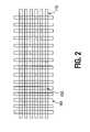
- FIG. 2shows a top plan view of one embodiment of the layout of the word lines/select lines of the present invention.
- FIG. 3shows a cross-sectional view of one embodiment of a fabrication step in accordance with the magnetic memory device of FIG. 1 .
- FIG. 4shows a cross-sectional view of one embodiment of another fabrication step in accordance with the magnetic memory device of FIG. 1 .
- FIG. 5shows a cross-sectional view of one embodiment of another fabrication step in accordance with the magnetic memory device of FIG. 1 .
- FIG. 6shows a cross-sectional view of one embodiment of another fabrication step in accordance with the magnetic memory device of FIG. 1 .
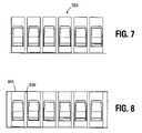
- FIG. 7shows a cross-sectional view of one embodiment of another fabrication step in accordance with the magnetic memory device of FIG. 1 .
- FIG. 8shows a cross-sectional view of one embodiment of another fabrication step in accordance with the magnetic memory device of FIG. 1 .
- FIG. 9shows a cross-sectional view of one embodiment of a programming operation of the present invention.
- FIG. 10shows a cross-sectional view of one embodiment of the programming operation of the present invention.
- FIG. 11shows a cross-sectional view of one embodiment of an erase method of the present invention.
- FIG. 12shows a cross-sectional view of one embodiment of the erase method of the present invention.
- FIG. 13shows a cross-sectional view of one embodiment of the magnetic memory cell in a NOR configuration.
- FIG. 14shows a top plan view of one embodiment of a NOR layout of control lines in accordance with the embodiment of FIG. 13 .
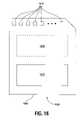
- FIG. 15shows a block diagram of an electronic memory system of the present invention.
- FIG. 16shows a block diagram of one embodiment of a memory module of the present invention.
- FIG. 17shows a plot of time versus write voltage V write including the refresh cycle for a DRAM embodiment of the present invention.
- SOSsilicon-on-sapphire
- SOIsilicon-on-insulator
- TFTthin film transistor
- doped and undoped semiconductorsepitaxial layers of a silicon supported by a base semiconductor structure, as well as other semiconductor structures well known to one skilled in the art.
- wafer or substratewhen reference is made to a wafer or substrate in the following description, previous process steps may have been utilized to form regions/junctions in the base semiconductor structure, and terms wafer or substrate include the underlying layers containing such regions/junctions.
- the semiconductor magnetic memory device of the present inventionis comprised of a memory array that incorporates floating gate memory cells with a magnetic tunnel junction (MTJ) layer.
- the MTJ layeruses the Giant Magneto Resistance Effect to turn on and off each cell, thus allowing access to the floating gate for storage of a charge.
- FIG. 1illustrates a cross-sectional view of one embodiment of the structure of the magnetic memory device of the present invention.
- the embodiment of FIG. 1is for a NAND architecture memory array. In the interest of clarity, only one cell structure will be described. However, each cell of the magnetic memory array of the present invention is constructed in substantially the same way.
- Each cell 100is comprised of a floating gate 120 that wraps around the control gate 101 , 102 .
- the floating gate 120is comprised of polysilicon. Alternate embodiments can use other materials.
- a tunnel insulator layer 123in one embodiment, is formed of an oxide material under the floating gate. Alternate embodiments can use other insulator materials.
- the control gate/word line 101 , 102is located within the floating gate 120 .
- the control gateis comprised of two layers 101 , 102 .
- the upper layerin one embodiment, is a tungsten silicide (WSi x ) layer 101 . Tungsten silicide may also be referred to in the art as polycide.
- the lower layer 102in one embodiment, is comprised of polysilicon. Alternate embodiments can use other materials for either of these layers.
- FIG. 1shows arrows coming out of the plane of the paper to indicate that the axis of the word lines extends into and out of the plane of the figure.
- An insulating layer of nitride 122is formed around the control gate 101 , 102 . This layer insulates the control gate 101 , 102 from the floating gate 120 .
- An oxide-nitride-oxide layer 121is formed at the bottom of the control gate 101 , 102 to further separate the control gate 101 , 102 and the floating gate 120 .
- the MTJcan be comprised of an antiferromagnetic layer separated from a ferromagnetic layer by a relatively thin dielectric material.
- the dielectricshould be thin enough to allow spin dependent electron tunneling while still forming a robust barrier to electrons that are not spin polarized. Also, it is desirable that the materials used for the barrier do not translate crystalline structure or contribute magnetic properties to the MTJ.
- the MTJ layeris formed over the floating gate 120 of each cell 100 .
- the pinning layer 103Immediately adjacent to the floating gate is the pinning layer 103 .
- This layer 103can be comprised of a synthetic antiferromagnet such as combinations of manganese and a metal. Combinations can include irridium manganese, platinum manganese, iron manganese, and chromium platinum manganese.
- the pinning layer 103is responsible for fixing the magnetic orientation of the lower magnetic layer 106 . Alternate embodiments can use other materials and/or material combinations for this layer 103 .
- the lower magnetic layer 106is therefore the fixed magnetic layer 106 while the upper magnetic layer 107 changes magnetic orientation in response to the current flow as described subsequently with reference to the programming and erasing methods of FIGS. 10-13 .
- Both the fixed magnetic layer 106 and the free magnetic layer 107can be comprised of high susceptibility magnetic material such as cobalt, iron, or nickel. Additionally, combinations of these materials can be used to enhance their magnetic properties such as nickel iron and cobalt iron. Niobium, hafnium, and boron may be used in varying combinations to prevent migration or dilution of the magnetic materials at the interface boundaries. Alternate embodiments can use other materials and/or material combinations for these layers.
- a tunneling barrier 105is formed between the fixed magnetic layer 106 and the free magnetic layer 107 .
- the tunneling barrier 105is a relatively thin dielectric film that separates the two magnetic layers 106 , 107 .
- the tunneling barrier 105is comprised of an oxide material such as aluminum oxide, titanium oxide, or manganese oxide. Additionally, materials such as silicon dioxide or hafnium oxide can be used. Alternate embodiments can use other materials for this layer 105 that do not introduce undesirable magnetic properties.
- An optional layer of relatively thin rutheniumcan be inserted between the antiferromagnetic layer and the ferromagnetic layer in order to enhance the magnetic coupling of the synthetic antiferromagnet.
- Other oscillatory exchange materialscan include chromium, rhodium, iridium copper and their alloys.
- the free magnetic layer 107makes contact with a top electrode 105 .
- the electrode 105provides contact between the MTJ stack 103 , 104 , 106 , 107 and the program/erase line 109 .
- the electrodeis comprised of a metal material. Alternate embodiments can use other materials.
- the program/erase line 109is a single line that is orthogonal to the word lines of the array and ties together the series string columns of the array.
- the cell select line 1 10is formed parallel to and above the program/erase line 109 .
- These lines 109 , 110are separated by an insulating material 111 such as an oxide material.
- the cell select line 110is responsible for switching the magnetization of the free magnetic layer 107 of the MTJ layer.
- the orthogonality of the cell select lines 110 with the word lines 101 , 102provides the necessary selectivity require to program and erase each individual cell.
- the operation of the program/erase line 109 and the cell select line 1 10is discussed further subsequently with reference to the program and erase embodiments of FIGS. 10-13 .
- Cross-talk between cells 100 , 160may be substantially reduced or eliminated by the addition of a thin layer of magnetic material that acts as a magnetic spacer 150 .
- the spacersenhance the ability to reduce both cell spacing and cell size.
- This strategyuses high permeability materials such as nickel, iron, cobalt, or combinations of these materials to confine the magnetic flux produced by the MTJ devices.
- High permeability “flux keepers”are often applied to both increase the switching efficiency of the MTJ as well as reduce unwanted stray magnetic fields that may affect the performance or readability of adjacent bits.
- FIG. 2illustrate a top plan view of one embodiment of the layout for the word lines and cell select/program erase lines of the present invention.
- the word lines 101are shown running in the “y” direction. These lines include both the upper polycide layer 101 of the word line and the lower polysilicon layer 102 .
- the cell select line 110is shown running perpendicular to the word lines 101 in the “x” direction. The cell select line 110 is over the program/erase line 109 . The intersection of each of the word lines and each of the select/program lines 101 , 110 is over a memory cell 100 as described previously and shown in FIG. 1 .
- FIG. 3illustrates a cross-sectional view of one embodiment of fabrication steps for the magnetic memory device of the present invention.
- a polysilicon layer 301is formed over a tunneling layer 310 .
- the tunneling layer 310is an oxide. Alternate embodiments can use other insulating materials.
- the floating gate cell structureis comprised of an oxide 320 layer formed over the polysilicon layer 301 .
- a nitride layer 321is formed over the oxide layer.
- a second oxide layer 322is formed over the nitride layer 321 .
- These three layer 320 - 322together form the ONO 320 insulator structure of the floating gate cell.
- the ONOcan be replaced by a high-K or a combination of high-K and ONO layers to increase coupling capacitance between the word line and the substrate thereby reducing the operational voltages of these
- a poly silicon layer 303is formed over the ONO layer 302 and a polycide (WSi x ) layer 305 is formed over the poly layer 303 . Together these layer 303 , 305 form the control gate/word line structure of the floating gate cell.
- FIG. 4illustrates a cross-sectional view of one embodiment of additional fabrication steps for the magnetic memory device of the present invention.
- a nitride spacer 400is formed over the structure of FIG. 3 .
- FIG. 5An in situ nitride and polysilicon etch is then performed in FIG. 5 . This step removes portions of the nitride layer 400 of FIG. 4 and portions of the poly silicon layer 301 between each floating gate structure 300 . This exposes the oxide layer 310 between each floating gate structure 300 .
- FIG. 7shows the results of an in situ polysilicon etch and tunnel oxide etch of the tunnel oxide layer 310 . This step forms the individual floating gates 700 that surround each cell structure. The tunnel oxide etch isolates each tunnel oxide layer for each individual cell.
- FIG. 8a structure insulator 800 is then formed between each of the floating gate structures. This may be a low-k insulator. Also in this step, a nitride barrier 801 may be formed over the structure to act as a chemical mechanical planarization (CMP) stop layer for future steps.
- CMPchemical mechanical planarization
- a magnetic tunnel junction deposition and patterningis then performed to form the MTJ junction over each floating gate cell structure.
- Electrode deposition and program/erase line deposition with patterningforms the individual electrodes and program/erase line over each cell.
- the cell select lineis then deposited over the oxide insulating layer and patterned, thus resulting in the structure illustrated in FIG. 1 .
- FIG. 9illustrates a schematic cross-sectional view of one embodiment of a programming operation of the magnetic memory device of the present invention.
- the programmingis performed by isolating a desired MTJ stack of the cell to be programmed. This is accomplished by passing currents through the specific cell select line 901 and word line 903 that are coupled to the cell to be programmed.
- the current through the cell select line 901is denoted as I 1 and the current through the word line is denoted as I 2 .
- I 1 and I 2each create magnetic fields in the directions as shown in FIG. 9 .
- the magnetic filed created by I 1causes the magnetic filed in the free magnetic layer 910 to orient in the direction of magnetization of the lower pinned layer 911 . This is referred to in the art as the “easy axis”. This axis is illustrated in FIG. 10 .
- Current I 2causes the magnetization of the free magnetic layer 910 to orient orthogonal to the direction of the pinned layer 911 .
- This axisis referred to as the “hard axis” as illustrated in FIG. 10 .
- V writeis then applied on the program/erase line 905 .
- Thiscauses electrons 1003 to pass to the floating gate 1005 as a stored charge.
- the charge, Qcan be determined by (V write /R MTJ )* ⁇ t where R MTJ is the resistance of the stack and ⁇ t is the time of the programming pulse.
- the programming timecan be measured in nanoseconds, depending on V write and the resistance of the MTJ.
- V writeis a programming pulse with an amplitude in the range of 3V-10V.
- the V write voltagesare substantially lower than what current flash memory parts use. This is a direct result of using an MTJ to program the cells instead of the power intensive Fowler-Nordheim approach or channel hot electron injection.
- V writecan start at a lower write voltage and increase incrementally by a step voltage for any subsequent programming pulses required to properly program the non-volatile cell.
- a variety of chargescan be stored into the magnetic memory device of the present invention.
- a plurality of threshold voltagescan be programmed into the cell simply by opening the MTJ for a predetermined time period. This allows the memory cells of the present invention to operate as either single level cells or multiple level cells.
- the tunnel oxideis not damaged during programming.
- the reliability of the tunnel oxideis increased over a typical flash memory device and the number of program cycles is infinite.
- FIGS. 11 and 12illustrate schematic cross-sectional views of one embodiment of a method for erasing the magnetic memory devices of the present invention.
- the erase operationis substantially similar to the program operation as previously described.
- One differenceis that the program/erase line 1101 is grounded or biased at a voltage level that is only slightly positive.
- the resistance of the MTJ 1102is reduced by the magnetic fields generated by currents I 1 through the cell select line 1100 and I 2 through the word line 1105 .
- the ground or slightly positive biasing of the program/erase line 1101attracts the electrons 1203 from the floating gate 1201 .
- Reading the memory cells of the present inventionis accomplished by a current flowing in the opposite direction than the program/erase operations. This “raises” the MTJ to its highest resistance state and prevents any leakage of charge. A stored charge on the floating gate of the memory cell causes a V t shift that, with the proper combination of voltage on the substrate, drain region, and source region, will cause it to be read as a logical “0” or a logical “1”. Similar techniques can be used to read the states of multiple level cells.
- the word lineis biased at 4.5V and the cell select line is biased at ground potential.
- the substrateis also at ground potential.
- the digit linewhich is also referred to as a bit line, is coupled to the drain regions and is biased at 0.1V.
- the program/erase lineis left floating.
- the above embodimentsillustrated a NAND architecture memory array.
- the magnetic memory cells of the present inventioncan also be incorporated into a NOR architecture memory array as illustrated in FIGS. 13 and 14 .
- FIG. 13illustrates a cross-sectional view of a NOR embodiment of the magnetic non-volatile memory cells of the present invention. This view is across the active areas.
- the cell structure 1300is substantially similar as that described previously.
- the cell select line 1310acts as a digit line. It is coupled to digit line contacts 1307 that couple the cell's drain regions 1305 to the select line 1310 . In this view, the digit line contact 1307 is formed behind the program/erase line 1309 .
- a common source line 1303is formed in the substrate between rows of memory cells.
- a low-k inter-level dielectric 1304is formed between cells and over the common source lines 1303 .
- the NOR embodiment of the semiconductor magnetic memorycan act as a DRAM memory array as well. This can be the case where the MTJs are sufficiently thin and allow charge to bleed through them via direct tunneling mechanisms. As a result, the memory cell loses charge from its floating gate. This then needs to be replenished with the help of a refresh cycle. Thus, the memory cell behaves as a volatile or non-volatile memory, depending on the MTJ “OFF” state leakage behavior.
- the idea of refreshis illustrated in FIG. 17 .
- FIG. 17illustrates a plot of time versus the write voltage, V write .
- V tis the threshold voltage dividing the logical “0” state from the logical “1” state.
- FIG. 14illustrates a top plan view of one embodiment of a layout of the NOR array of the present invention.
- the layoutis comprised of the drain regions 1305 and common source lines 1303 as illustrated in the embodiment of FIG. 13 .
- the program/erase lines 1309 and underlying digit lines 1310are shown.
- a memory cell 1400is formed at the intersection of each word line 1401 with the program/erase lines 1309 and digit lines 1310 .
- FIG. 15illustrates a functional block diagram of a memory system 1520 comprising a memory device 1500 coupled to a processor 1510 .
- the processor 1510may be a microprocessor or some other type of controlling circuitry. They memory system 1520 can be made up of separate integrated circuits or both the processor 1510 and memory device 1500 on the same integrated circuit.
- the memory device 1500has been simplified to focus on features of the memory that are helpful in understanding the present invention.
- the memory deviceincludes an array of memory cells 1530 incorporating the magnetic memory cells of the present invention.
- the memory array 1530can be a random access memory array (RAM) such as a dynamic random access memory array (DRAM), a flash memory array, or some other memory technology.
- RAMrandom access memory array
- DRAMdynamic random access memory array
- flash memory arrayor some other memory technology.
- the memory cellscan be non-volatile flash memory cells, volatile memory cells, or a combination of volatile and non-volatile cells.
- the memory array 1530is arranged in banks of rows and columns.
- the control gates of each row of memory cellsare coupled with a word line while the drain regions of the memory cells are coupled to bit lines.
- the source regions of the memory cellsare coupled to source lines.
- the connection of the cells to the bit lines and source linesdepends on whether the array is a NAND architecture, a NOR architecture, an AND architecture or some other memory array architecture.
- a CEL_SEL driver circuit 1556is coupled to the address circuitry to generate the currents required for the CEL_SEL lines of the memory array 1530 .
- the output of the CEL_SEL circuit 1556is coupled to the CEL_SEL lines that have been previously described.
- an address buffer circuit 1540is provided to latch address signals provided over I/O connections 1562 through the I/O circuitry 1560 . Address signals are received and decoded by a row decoder 1544 and a column decoder 1546 to access the memory array 1530 .
- the word line/row decoder 1544can be a current source as well as a voltage source. It will be appreciated by those skilled in the art that, with the benefit of the present description, the number of address input connections depends on the density and architecture of the memory array 1530 . That is, the number of addresses increases with both increased memory cell counts and increased bank and block counts.
- the memory integrated circuit 1500reads data in the memory array 1530 by sensing voltage or current changes in the memory array columns using sense/buffer circuitry 1550 .
- the sense/buffer circuitryin one embodiment, is coupled to read and latch a row of data from the memory array 1530 .
- Data input and output buffer circuitry 1560is included for bi-directional data communication over the I/O connections 1562 with the processor 1510 .
- Write circuitry 1555is provided to write data to the memory array.
- Control circuitry 1570decodes signals provided on control connections 1572 from the processor 1510 . These signals include chip enable signals, write enable signals, and address latch signals that are used to control the operations on the memory array 1530 , including data read, data write, and erase operations. In one embodiment, the control circuitry 1570 is responsible for executing the programming, erase, and read operations of the present invention.
- the control circuitry 1570may be a state machine, a sequencer, or some other type of controller.
- FIG. 15has been simplified to facilitate a basic understanding of the features of the memory. A more detailed understanding of internal circuitry and functions of flash memories are known to those skilled in the art.
- FIG. 16is an illustration of an exemplary memory module 1600 .
- Memory module 1600is illustrated as a memory card, although the concepts discussed with reference to memory module 1600 are applicable to other types of removable or portable memory, e.g., USB flash drives, and are intended to be within the scope of “memory module” as used herein.
- memory modulee.g., USB flash drives
- FIG. 16shows one example form factor, these concepts are applicable to other form factors as well.
- the memory module 1600includes a housing 1605 (as depicted) to enclose one or more memory devices 1610 , though such a housing is not essential to all devices or device applications. At least one memory device 1610 is a non-volatile memory [including or adapted to perform elements of the invention].
- the housing 1605includes one or more contacts 1615 for communication with a host device. Examples of host devices include digital cameras, digital recording and playback devices, PDAs, personal computers, memory card readers, interface hubs ad the like.
- the contacts 1615are in the form of a standardized interface. For example, with a USB flash drive, the contacts 1615 might be in the form of a USB Type-A male connector.
- the contacts 1615are in the form of a semi-proprietary interface, such as might be found on COMPACTFLASH memory cards licensed by SANDISK Corporation, MEMORYSTICK memory cards licensed by SONY Corporation, SD SECURE DIGITAL memory cards licensed by TOSHIBA Corporation and the like. In general, however, contacts 1615 provide an interface for passing control, address and/or data signals between the memory module 1600 and a host having compatible receptors for the contacts 1615 .
- the memory module 1600may optionally include additional circuitry 1620 that may be one or more integrated circuits and/or discrete components.
- the additional circuitry 1620may include a memory controller for controlling access across multiple memory devices 1610 and/or for providing a translation layer between an external host and a memory device 1610 .
- a memory controllercould selectively couple an I/O connection (not shown in FIG. 16 ) of a memory device 1610 to receive the appropriate signal at the appropriate I/O connection at the appropriate time or to provide the appropriate signal at the appropriate contact 1615 at the appropriate time.
- the communication protocol between a host and the memory module 1600may be different than what is required for access of a memory device 1610 .
- a memory controllercould then translate the command sequences received from a host into the appropriate command sequences to achieve the desired access to the memory device 1610 .
- Such translationmay further include changes in signal voltage levels in addition to command sequences.
- the additional circuitry 1620may further include functionality unrelated to control of a memory device 1610 such as a logic functions as might be performed by an ASIC (application specific integrated circuit). Also, the additional circuitry 1620 may include circuitry to restrict read or write access to the memory module 1600 , such as password protection, biometrics or the like. The additional circuitry 1620 may include circuitry to indicate a status of the memory module 1600 . For example, the additional circuitry 1620 may include functionality to determine whether power is being supplied to the memory module 1600 and whether the memory module 1600 is currently being accessed, and to display an indication of its status, such as a solid light while powered and a flashing light while being accessed. The additional circuitry 1620 may further include passive devices, such as decoupling capacitors to help regulate power requirements within the memory module 1600 .
- the embodiments of the present inventionprovide a semiconductor magnetic memory device incorporating a magnetic tunneling junction to control access to a memory cell structure.
- the memory celluses a floating gate that wraps around the control gate/word line to enable the floating gate to directly contact the lower layer of the MTJ.
Landscapes
- Engineering & Computer Science (AREA)
- Computer Hardware Design (AREA)
- Microelectronics & Electronic Packaging (AREA)
- Non-Volatile Memory (AREA)
- Read Only Memory (AREA)
- Mram Or Spin Memory Techniques (AREA)
- Semiconductor Memories (AREA)
Abstract
Description
- The present invention relates generally to memory devices and in particular the present invention relates to semiconductor magnetic memory architecture.
- Memory devices are typically provided as internal, semiconductor, integrated circuits in computers or other electronic devices. There are many different types of memory including random-access memory (RAM), read only memory (ROM), dynamic random access memory (DRAM), synchronous dynamic random access memory (SDRAM), and flash memory.
- Flash memory devices have developed into a popular source of non-volatile memory for a wide range of electronic applications. Flash memory devices typically use a one-transistor memory cell that allows for high memory densities, high reliability, and low power consumption. Common uses for flash memory include personal computers, personal digital assistants (PDAs), digital cameras, and cellular telephones. Program code and system data such as a basic input/output system (BIOS) are typically stored in flash memory devices for use in personal computer systems.
- As the performance and complexity of electronic systems increase, the speed of the system memory needs to increase as well. However, one of the disadvantages of flash memory is the slow programming and erase speeds. Typical prior art programming uses either Fowler-Nordheim tunneling or hot electron injection to move a charge from a channel in the substrate onto the floating gate. The mechanism by which they tunnel through the oxide/insulator layer damages the layer. This limits the number of times that a flash memory device can be programmed reliably before the dielectric wears out and loses its insulating properties.
- The flash road map requires a memory cell structure change due to the scaling limitations of the floating gate technology. The floating gate stack has a problem with capacitive coupling to neighboring cells causing disturb problems. By lowering the stack height, the capacitance can be reduced. One approach is to eliminate the floating gate and use a SONOS approach to storing charge in the dielectric layer itself. A second approach that enhances the SONOS structure is to add nano-crystals under the word line poly.
- For the reasons stated above, and for other reasons stated below which will become apparent to those skilled in the art upon reading and understanding the present specification, there is a need in the art for a memory device that operates faster and has a longer life.
FIG. 1 shows a cross-sectional view of one embodiment of a semiconductor magnetic memory device of the present invention.FIG. 2 shows a top plan view of one embodiment of the layout of the word lines/select lines of the present invention.FIG. 3 shows a cross-sectional view of one embodiment of a fabrication step in accordance with the magnetic memory device ofFIG. 1 .FIG. 4 shows a cross-sectional view of one embodiment of another fabrication step in accordance with the magnetic memory device ofFIG. 1 .FIG. 5 shows a cross-sectional view of one embodiment of another fabrication step in accordance with the magnetic memory device ofFIG. 1 .FIG. 6 shows a cross-sectional view of one embodiment of another fabrication step in accordance with the magnetic memory device ofFIG. 1 .FIG. 7 shows a cross-sectional view of one embodiment of another fabrication step in accordance with the magnetic memory device ofFIG. 1 .FIG. 8 shows a cross-sectional view of one embodiment of another fabrication step in accordance with the magnetic memory device ofFIG. 1 .FIG. 9 shows a cross-sectional view of one embodiment of a programming operation of the present invention.FIG. 10 shows a cross-sectional view of one embodiment of the programming operation of the present invention.FIG. 11 shows a cross-sectional view of one embodiment of an erase method of the present invention.FIG. 12 shows a cross-sectional view of one embodiment of the erase method of the present invention.FIG. 13 shows a cross-sectional view of one embodiment of the magnetic memory cell in a NOR configuration.FIG. 14 shows a top plan view of one embodiment of a NOR layout of control lines in accordance with the embodiment ofFIG. 13 .FIG. 15 shows a block diagram of an electronic memory system of the present invention.FIG. 16 shows a block diagram of one embodiment of a memory module of the present invention.FIG. 17 shows a plot of time versus write voltage Vwriteincluding the refresh cycle for a DRAM embodiment of the present invention.- In the following detailed description of the invention, reference is made to the accompanying drawings that form a part hereof and in which is shown, by way of illustration, specific embodiments in which the invention may be practiced. In the drawings, like numerals describe substantially similar components throughout the several views. These embodiments are described in sufficient detail to enable those skilled in the art to practice the invention. Other embodiments may be utilized and structural, logical, and electrical changes may be made without departing from the scope of the present invention. The following detailed description is, therefore, not to be taken in a limiting sense, and the scope of the present invention is defined only by the appended claims and equivalents thereof. The terms wafer or substrate used in the following description include any base semiconductor structure. Both are to be understood as including silicon-on-sapphire (SOS) technology, silicon-on-insulator (SOI) technology, thin film transistor (TFT) technology, doped and undoped semiconductors, epitaxial layers of a silicon supported by a base semiconductor structure, as well as other semiconductor structures well known to one skilled in the art. Furthermore, when reference is made to a wafer or substrate in the following description, previous process steps may have been utilized to form regions/junctions in the base semiconductor structure, and terms wafer or substrate include the underlying layers containing such regions/junctions.
- The semiconductor magnetic memory device of the present invention is comprised of a memory array that incorporates floating gate memory cells with a magnetic tunnel junction (MTJ) layer. The MTJ layer uses the Giant Magneto Resistance Effect to turn on and off each cell, thus allowing access to the floating gate for storage of a charge.
FIG. 1 illustrates a cross-sectional view of one embodiment of the structure of the magnetic memory device of the present invention. The embodiment ofFIG. 1 is for a NAND architecture memory array. In the interest of clarity, only one cell structure will be described. However, each cell of the magnetic memory array of the present invention is constructed in substantially the same way.- Each
cell 100 is comprised of afloating gate 120 that wraps around thecontrol gate floating gate 120 is comprised of polysilicon. Alternate embodiments can use other materials. - A
tunnel insulator layer 123, in one embodiment, is formed of an oxide material under the floating gate. Alternate embodiments can use other insulator materials. - The control gate/
word line floating gate 120. The control gate is comprised of twolayers layer 101. Tungsten silicide may also be referred to in the art as polycide. Thelower layer 102, in one embodiment, is comprised of polysilicon. Alternate embodiments can use other materials for either of these layers. - The control gates of each cell are coupled together by the word lines of the array.
FIG. 1 shows arrows coming out of the plane of the paper to indicate that the axis of the word lines extends into and out of the plane of the figure. - An insulating layer of
nitride 122 is formed around thecontrol gate control gate gate 120. An oxide-nitride-oxide layer 121 is formed at the bottom of thecontrol gate control gate gate 120. - The MTJ can be comprised of an antiferromagnetic layer separated from a ferromagnetic layer by a relatively thin dielectric material. The dielectric should be thin enough to allow spin dependent electron tunneling while still forming a robust barrier to electrons that are not spin polarized. Also, it is desirable that the materials used for the barrier do not translate crystalline structure or contribute magnetic properties to the MTJ.
- The MTJ layer is formed over the floating
gate 120 of eachcell 100. Immediately adjacent to the floating gate is the pinninglayer 103. Thislayer 103 can be comprised of a synthetic antiferromagnet such as combinations of manganese and a metal. Combinations can include irridium manganese, platinum manganese, iron manganese, and chromium platinum manganese. The pinninglayer 103 is responsible for fixing the magnetic orientation of the lower magnetic layer106. Alternate embodiments can use other materials and/or material combinations for thislayer 103. - The lower magnetic layer106 is therefore the fixed magnetic layer106 while the upper
magnetic layer 107 changes magnetic orientation in response to the current flow as described subsequently with reference to the programming and erasing methods ofFIGS. 10-13 . Both the fixed magnetic layer106 and the freemagnetic layer 107 can be comprised of high susceptibility magnetic material such as cobalt, iron, or nickel. Additionally, combinations of these materials can be used to enhance their magnetic properties such as nickel iron and cobalt iron. Niobium, hafnium, and boron may be used in varying combinations to prevent migration or dilution of the magnetic materials at the interface boundaries. Alternate embodiments can use other materials and/or material combinations for these layers. - A
tunneling barrier 105 is formed between the fixed magnetic layer106 and the freemagnetic layer 107. Thetunneling barrier 105 is a relatively thin dielectric film that separates the twomagnetic layers 106,107. In one embodiment, thetunneling barrier 105 is comprised of an oxide material such as aluminum oxide, titanium oxide, or manganese oxide. Additionally, materials such as silicon dioxide or hafnium oxide can be used. Alternate embodiments can use other materials for thislayer 105 that do not introduce undesirable magnetic properties. - An optional layer of relatively thin ruthenium can be inserted between the antiferromagnetic layer and the ferromagnetic layer in order to enhance the magnetic coupling of the synthetic antiferromagnet. Other oscillatory exchange materials can include chromium, rhodium, iridium copper and their alloys.
- The free
magnetic layer 107 makes contact with atop electrode 105. Theelectrode 105 provides contact between theMTJ stack line 109. In one embodiment, the electrode is comprised of a metal material. Alternate embodiments can use other materials. - The program/erase
line 109 is a single line that is orthogonal to the word lines of the array and ties together the series string columns of the array. The cellselect line 110 is formed parallel to and above the program/eraseline 109. Theselines material 111 such as an oxide material. - The cell
select line 110 is responsible for switching the magnetization of the freemagnetic layer 107 of the MTJ layer. The orthogonality of the cellselect lines 110 with the word lines101,102 provides the necessary selectivity require to program and erase each individual cell. The operation of the program/eraseline 109 and the cellselect line 110 is discussed further subsequently with reference to the program and erase embodiments ofFIGS. 10-13 . - Cross-talk between
cells magnetic spacer 150. The spacers enhance the ability to reduce both cell spacing and cell size. This strategy uses high permeability materials such as nickel, iron, cobalt, or combinations of these materials to confine the magnetic flux produced by the MTJ devices. High permeability “flux keepers” are often applied to both increase the switching efficiency of the MTJ as well as reduce unwanted stray magnetic fields that may affect the performance or readability of adjacent bits. FIG. 2 illustrate a top plan view of one embodiment of the layout for the word lines and cell select/program erase lines of the present invention. The word lines101 are shown running in the “y” direction. These lines include both theupper polycide layer 101 of the word line and thelower polysilicon layer 102. The cellselect line 110 is shown running perpendicular to the word lines101 in the “x” direction. The cellselect line 110 is over the program/eraseline 109. The intersection of each of the word lines and each of the select/program lines memory cell 100 as described previously and shown inFIG. 1 .- The following fabrication steps and materials for the magnetic memory device of the present invention are for purposes of illustration only. Alternate embodiments can use other materials than those disclosed and different fabrication steps in forming the structure of the present invention.
FIG. 3 illustrates a cross-sectional view of one embodiment of fabrication steps for the magnetic memory device of the present invention. Apolysilicon layer 301 is formed over atunneling layer 310. In one embodiment, thetunneling layer 310 is an oxide. Alternate embodiments can use other insulating materials.- The floating gate cell structure is comprised of an
oxide 320 layer formed over thepolysilicon layer 301. Anitride layer 321 is formed over the oxide layer. Asecond oxide layer 322 is formed over thenitride layer 321. These three layer320-322 together form theONO 320 insulator structure of the floating gate cell. The ONO can be replaced by a high-K or a combination of high-K and ONO layers to increase coupling capacitance between the word line and the substrate thereby reducing the operational voltages of these - A
poly silicon layer 303 is formed over the ONO layer302 and a polycide (WSix)layer 305 is formed over thepoly layer 303. Together theselayer FIG. 4 illustrates a cross-sectional view of one embodiment of additional fabrication steps for the magnetic memory device of the present invention. In this figure, anitride spacer 400 is formed over the structure ofFIG. 3 .- An in situ nitride and polysilicon etch is then performed in
FIG. 5 . This step removes portions of thenitride layer 400 ofFIG. 4 and portions of thepoly silicon layer 301 between each floatinggate structure 300. This exposes theoxide layer 310 between each floatinggate structure 300. - A
blanket polysilicon 600 deposition is then performed as shown inFIG. 6 .FIG. 7 shows the results of an in situ polysilicon etch and tunnel oxide etch of thetunnel oxide layer 310. This step forms the individual floatinggates 700 that surround each cell structure. The tunnel oxide etch isolates each tunnel oxide layer for each individual cell. FIG. 8 astructure insulator 800 is then formed between each of the floating gate structures. This may be a low-k insulator. Also in this step, anitride barrier 801 may be formed over the structure to act as a chemical mechanical planarization (CMP) stop layer for future steps.- A magnetic tunnel junction deposition and patterning is then performed to form the MTJ junction over each floating gate cell structure. Electrode deposition and program/erase line deposition with patterning forms the individual electrodes and program/erase line over each cell. The cell select line is then deposited over the oxide insulating layer and patterned, thus resulting in the structure illustrated in
FIG. 1 . FIG. 9 illustrates a schematic cross-sectional view of one embodiment of a programming operation of the magnetic memory device of the present invention. The programming is performed by isolating a desired MTJ stack of the cell to be programmed. This is accomplished by passing currents through the specific cellselect line 901 andword line 903 that are coupled to the cell to be programmed. The current through the cellselect line 901 is denoted as I1and the current through the word line is denoted as I2.- Currents I1and I2each create magnetic fields in the directions as shown in
FIG. 9 . The magnetic filed created by I1causes the magnetic filed in the freemagnetic layer 910 to orient in the direction of magnetization of the lower pinnedlayer 911. This is referred to in the art as the “easy axis”. This axis is illustrated inFIG. 10 . - Current I2causes the magnetization of the free
magnetic layer 910 to orient orthogonal to the direction of the pinnedlayer 911. This axis is referred to as the “hard axis” as illustrated inFIG. 10 . - This combination of easy and hard axis orientation of the magnetic domains in the
free layer 910 causes the resistance of the MTJ stack to drop at lower magnetic fields as compared to typical prior art stacks where the domains are oriented parallel/anti-parallel to each other. Additional information regarding orthogonal programming of easy and hard axes can be found in Tehrani et al., Proc. IEEE 91(5), (2003), pp. 703. - As shown in
FIG. 10 , a voltage Vwriteis then applied on the program/eraseline 905. This causeselectrons 1003 to pass to the floatinggate 1005 as a stored charge. The charge, Q, can be determined by (Vwrite/RMTJ)*Δt where RMTJis the resistance of the stack and Δt is the time of the programming pulse. In one embodiment, the programming time can be measured in nanoseconds, depending on Vwriteand the resistance of the MTJ. - In one embodiment, Vwriteis a programming pulse with an amplitude in the range of 3V-10V. The Vwritevoltages are substantially lower than what current flash memory parts use. This is a direct result of using an MTJ to program the cells instead of the power intensive Fowler-Nordheim approach or channel hot electron injection. Vwritecan start at a lower write voltage and increase incrementally by a step voltage for any subsequent programming pulses required to properly program the non-volatile cell.
- By modulating the time Δt, a variety of charges can be stored into the magnetic memory device of the present invention. Thus a plurality of threshold voltages can be programmed into the cell simply by opening the MTJ for a predetermined time period. This allows the memory cells of the present invention to operate as either single level cells or multiple level cells.
- Since neither Fowler-Nordheim nor hot electron injection is used for programming the cells of the present invention, the tunnel oxide is not damaged during programming. Thus, the reliability of the tunnel oxide is increased over a typical flash memory device and the number of program cycles is infinite.
FIGS. 11 and 12 illustrate schematic cross-sectional views of one embodiment of a method for erasing the magnetic memory devices of the present invention. The erase operation is substantially similar to the program operation as previously described. One difference is that the program/eraseline 1101 is grounded or biased at a voltage level that is only slightly positive.- In the same manner as programming, the resistance of the
MTJ 1102 is reduced by the magnetic fields generated by currents I1through the cellselect line 1100 and I2through theword line 1105. The ground or slightly positive biasing of the program/eraseline 1101 attracts theelectrons 1203 from the floatinggate 1201. - Reading the memory cells of the present invention is accomplished by a current flowing in the opposite direction than the program/erase operations. This “raises” the MTJ to its highest resistance state and prevents any leakage of charge. A stored charge on the floating gate of the memory cell causes a Vtshift that, with the proper combination of voltage on the substrate, drain region, and source region, will cause it to be read as a logical “0” or a logical “1”. Similar techniques can be used to read the states of multiple level cells.
- In one embodiment, to read a single level cell, the word line is biased at 4.5V and the cell select line is biased at ground potential. The substrate is also at ground potential. The digit line, which is also referred to as a bit line, is coupled to the drain regions and is biased at 0.1V. The program/erase line is left floating.
- The above embodiments illustrated a NAND architecture memory array. The magnetic memory cells of the present invention can also be incorporated into a NOR architecture memory array as illustrated in
FIGS. 13 and 14 . FIG. 13 illustrates a cross-sectional view of a NOR embodiment of the magnetic non-volatile memory cells of the present invention. This view is across the active areas. Thecell structure 1300 is substantially similar as that described previously.- In this embodiment, the cell
select line 1310 acts as a digit line. It is coupled todigit line contacts 1307 that couple the cell'sdrain regions 1305 to theselect line 1310. In this view, thedigit line contact 1307 is formed behind the program/eraseline 1309. - A
common source line 1303 is formed in the substrate between rows of memory cells. In this embodiment, a low-k inter-level dielectric 1304 is formed between cells and over thecommon source lines 1303. - With the help of refresh circuitry used in DRAMs and is well known in the art, the NOR embodiment of the semiconductor magnetic memory can act as a DRAM memory array as well. This can be the case where the MTJs are sufficiently thin and allow charge to bleed through them via direct tunneling mechanisms. As a result, the memory cell loses charge from its floating gate. This then needs to be replenished with the help of a refresh cycle. Thus, the memory cell behaves as a volatile or non-volatile memory, depending on the MTJ “OFF” state leakage behavior. The idea of refresh is illustrated in
FIG. 17 . FIG. 17 illustrates a plot of time versus the write voltage, Vwrite. Vtis the threshold voltage dividing the logical “0” state from the logical “1” state.FIG. 14 illustrates a top plan view of one embodiment of a layout of the NOR array of the present invention. The layout is comprised of thedrain regions 1305 andcommon source lines 1303 as illustrated in the embodiment ofFIG. 13 . Also, the program/eraselines 1309 andunderlying digit lines 1310 are shown. As in the NAND embodiment, amemory cell 1400 is formed at the intersection of eachword line 1401 with the program/eraselines 1309 anddigit lines 1310.FIG. 15 illustrates a functional block diagram of amemory system 1520 comprising amemory device 1500 coupled to aprocessor 1510. Theprocessor 1510 may be a microprocessor or some other type of controlling circuitry. Theymemory system 1520 can be made up of separate integrated circuits or both theprocessor 1510 andmemory device 1500 on the same integrated circuit. Thememory device 1500 has been simplified to focus on features of the memory that are helpful in understanding the present invention.- The memory device includes an array of
memory cells 1530 incorporating the magnetic memory cells of the present invention. Thememory array 1530 can be a random access memory array (RAM) such as a dynamic random access memory array (DRAM), a flash memory array, or some other memory technology. The memory cells can be non-volatile flash memory cells, volatile memory cells, or a combination of volatile and non-volatile cells. - The
memory array 1530 is arranged in banks of rows and columns. The control gates of each row of memory cells are coupled with a word line while the drain regions of the memory cells are coupled to bit lines. The source regions of the memory cells are coupled to source lines. As is well known in the art, the connection of the cells to the bit lines and source lines depends on whether the array is a NAND architecture, a NOR architecture, an AND architecture or some other memory array architecture. - A
CEL_SEL driver circuit 1556 is coupled to the address circuitry to generate the currents required for the CEL_SEL lines of thememory array 1530. The output of theCEL_SEL circuit 1556 is coupled to the CEL_SEL lines that have been previously described. - In a NAND array, an
address buffer circuit 1540 is provided to latch address signals provided over I/O connections 1562 through the I/O circuitry 1560. Address signals are received and decoded by arow decoder 1544 and acolumn decoder 1546 to access thememory array 1530. The word line/row decoder 1544 can be a current source as well as a voltage source. It will be appreciated by those skilled in the art that, with the benefit of the present description, the number of address input connections depends on the density and architecture of thememory array 1530. That is, the number of addresses increases with both increased memory cell counts and increased bank and block counts. - The memory integrated
circuit 1500 reads data in thememory array 1530 by sensing voltage or current changes in the memory array columns using sense/buffer circuitry 1550. The sense/buffer circuitry, in one embodiment, is coupled to read and latch a row of data from thememory array 1530. Data input andoutput buffer circuitry 1560 is included for bi-directional data communication over the I/O connections 1562 with theprocessor 1510.Write circuitry 1555 is provided to write data to the memory array. Control circuitry 1570 decodes signals provided oncontrol connections 1572 from theprocessor 1510. These signals include chip enable signals, write enable signals, and address latch signals that are used to control the operations on thememory array 1530, including data read, data write, and erase operations. In one embodiment, thecontrol circuitry 1570 is responsible for executing the programming, erase, and read operations of the present invention. Thecontrol circuitry 1570 may be a state machine, a sequencer, or some other type of controller.- The memory device illustrated in
FIG. 15 has been simplified to facilitate a basic understanding of the features of the memory. A more detailed understanding of internal circuitry and functions of flash memories are known to those skilled in the art. FIG. 16 is an illustration of anexemplary memory module 1600.Memory module 1600 is illustrated as a memory card, although the concepts discussed with reference tomemory module 1600 are applicable to other types of removable or portable memory, e.g., USB flash drives, and are intended to be within the scope of “memory module” as used herein. In addition, although one example form factor is depicted inFIG. 16 , these concepts are applicable to other form factors as well.- In some embodiments, the
memory module 1600 includes a housing1605 (as depicted) to enclose one ormore memory devices 1610, though such a housing is not essential to all devices or device applications. At least onememory device 1610 is a non-volatile memory [including or adapted to perform elements of the invention]. Where present, thehousing 1605 includes one ormore contacts 1615 for communication with a host device. Examples of host devices include digital cameras, digital recording and playback devices, PDAs, personal computers, memory card readers, interface hubs ad the like. For some embodiments, thecontacts 1615 are in the form of a standardized interface. For example, with a USB flash drive, thecontacts 1615 might be in the form of a USB Type-A male connector. For some embodiments, thecontacts 1615 are in the form of a semi-proprietary interface, such as might be found on COMPACTFLASH memory cards licensed by SANDISK Corporation, MEMORYSTICK memory cards licensed by SONY Corporation, SD SECURE DIGITAL memory cards licensed by TOSHIBA Corporation and the like. In general, however,contacts 1615 provide an interface for passing control, address and/or data signals between thememory module 1600 and a host having compatible receptors for thecontacts 1615. - The
memory module 1600 may optionally includeadditional circuitry 1620 that may be one or more integrated circuits and/or discrete components. For some embodiments, theadditional circuitry 1620 may include a memory controller for controlling access acrossmultiple memory devices 1610 and/or for providing a translation layer between an external host and amemory device 1610. For example, there may not be a one-to-one correspondence between the number ofcontacts 1615 and a number of I/O connections to the one ormore memory devices 1610. Thus, a memory controller could selectively couple an I/O connection (not shown inFIG. 16 ) of amemory device 1610 to receive the appropriate signal at the appropriate I/O connection at the appropriate time or to provide the appropriate signal at theappropriate contact 1615 at the appropriate time. Similarly, the communication protocol between a host and thememory module 1600 may be different than what is required for access of amemory device 1610. A memory controller could then translate the command sequences received from a host into the appropriate command sequences to achieve the desired access to thememory device 1610. Such translation may further include changes in signal voltage levels in addition to command sequences. - The
additional circuitry 1620 may further include functionality unrelated to control of amemory device 1610 such as a logic functions as might be performed by an ASIC (application specific integrated circuit). Also, theadditional circuitry 1620 may include circuitry to restrict read or write access to thememory module 1600, such as password protection, biometrics or the like. Theadditional circuitry 1620 may include circuitry to indicate a status of thememory module 1600. For example, theadditional circuitry 1620 may include functionality to determine whether power is being supplied to thememory module 1600 and whether thememory module 1600 is currently being accessed, and to display an indication of its status, such as a solid light while powered and a flashing light while being accessed. Theadditional circuitry 1620 may further include passive devices, such as decoupling capacitors to help regulate power requirements within thememory module 1600. - In summary, the embodiments of the present invention provide a semiconductor magnetic memory device incorporating a magnetic tunneling junction to control access to a memory cell structure. The memory cell uses a floating gate that wraps around the control gate/word line to enable the floating gate to directly contact the lower layer of the MTJ.
- Although specific embodiments have been illustrated and described herein, it will be appreciated by those of ordinary skill in the art that any arrangement that is calculated to achieve the same purpose may be substituted for the specific embodiments shown. Many adaptations of the invention will be apparent to those of ordinary skill in the art. Accordingly, this application is intended to cover any adaptations or variations of the invention. It is manifestly intended that this invention be limited only by the following claims and equivalents thereof.
Claims (41)
Priority Applications (9)
| Application Number | Priority Date | Filing Date | Title |
|---|---|---|---|
| US11/447,709US7486550B2 (en) | 2006-06-06 | 2006-06-06 | Semiconductor magnetic memory integrating a magnetic tunneling junction above a floating-gate memory cell |
| PCT/US2007/013349WO2007146011A2 (en) | 2006-06-06 | 2007-06-06 | Semiconductor magnetic memory |
| CN2007800207236ACN101461064B (en) | 2006-06-06 | 2007-06-06 | Semiconductor magnetic memory |
| KR1020117003034AKR20110015705A (en) | 2006-06-06 | 2007-06-06 | Semiconductor magnetic memory |
| KR1020087029867AKR101036363B1 (en) | 2006-06-06 | 2007-06-06 | Semiconductor magnetic memory |
| GB0821824AGB2453274B (en) | 2006-06-06 | 2007-06-06 | Semiconductor magnetic memory |
| US12/360,496US7852668B2 (en) | 2006-06-06 | 2009-01-27 | Semiconductor magnetic memory integrating a magnetic tunneling junction above a floating-gate memory cell |
| US12/966,430US7995402B2 (en) | 2006-06-06 | 2010-12-13 | Method for erasing a semiconductor magnetic memory integrating a magnetic tunneling junction above a floating-gate memory cell |
| US13/186,796US8374037B2 (en) | 2006-06-06 | 2011-07-20 | Method for programming a semiconductor magnetic memory integrating a magnetic tunneling junction above a floating-gate memory cell |
Applications Claiming Priority (1)
| Application Number | Priority Date | Filing Date | Title |
|---|---|---|---|
| US11/447,709US7486550B2 (en) | 2006-06-06 | 2006-06-06 | Semiconductor magnetic memory integrating a magnetic tunneling junction above a floating-gate memory cell |
Related Child Applications (1)
| Application Number | Title | Priority Date | Filing Date |
|---|---|---|---|
| US12/360,496DivisionUS7852668B2 (en) | 2006-06-06 | 2009-01-27 | Semiconductor magnetic memory integrating a magnetic tunneling junction above a floating-gate memory cell |
Publications (2)
| Publication Number | Publication Date |
|---|---|
| US20070279977A1true US20070279977A1 (en) | 2007-12-06 |
| US7486550B2 US7486550B2 (en) | 2009-02-03 |
Family
ID=38662855
Family Applications (4)
| Application Number | Title | Priority Date | Filing Date |
|---|---|---|---|
| US11/447,709Active2027-03-30US7486550B2 (en) | 2006-06-06 | 2006-06-06 | Semiconductor magnetic memory integrating a magnetic tunneling junction above a floating-gate memory cell |
| US12/360,496Active2026-08-21US7852668B2 (en) | 2006-06-06 | 2009-01-27 | Semiconductor magnetic memory integrating a magnetic tunneling junction above a floating-gate memory cell |
| US12/966,430ActiveUS7995402B2 (en) | 2006-06-06 | 2010-12-13 | Method for erasing a semiconductor magnetic memory integrating a magnetic tunneling junction above a floating-gate memory cell |
| US13/186,796Active2026-06-27US8374037B2 (en) | 2006-06-06 | 2011-07-20 | Method for programming a semiconductor magnetic memory integrating a magnetic tunneling junction above a floating-gate memory cell |
Family Applications After (3)
| Application Number | Title | Priority Date | Filing Date |
|---|---|---|---|
| US12/360,496Active2026-08-21US7852668B2 (en) | 2006-06-06 | 2009-01-27 | Semiconductor magnetic memory integrating a magnetic tunneling junction above a floating-gate memory cell |
| US12/966,430ActiveUS7995402B2 (en) | 2006-06-06 | 2010-12-13 | Method for erasing a semiconductor magnetic memory integrating a magnetic tunneling junction above a floating-gate memory cell |
| US13/186,796Active2026-06-27US8374037B2 (en) | 2006-06-06 | 2011-07-20 | Method for programming a semiconductor magnetic memory integrating a magnetic tunneling junction above a floating-gate memory cell |
Country Status (5)
| Country | Link |
|---|---|
| US (4) | US7486550B2 (en) |
| KR (2) | KR20110015705A (en) |
| CN (1) | CN101461064B (en) |
| GB (1) | GB2453274B (en) |
| WO (1) | WO2007146011A2 (en) |
Cited By (10)
| Publication number | Priority date | Publication date | Assignee | Title |
|---|---|---|---|---|
| US20080237693A1 (en)* | 2007-03-30 | 2008-10-02 | Samsung Electronics Co., Ltd. | Storage of non-volatile memory device and method of forming the same |
| US20100038735A1 (en)* | 2008-08-18 | 2010-02-18 | Seagate Technology Llc | Magnet-assisted transistor devices |
| US7961503B2 (en) | 2009-01-19 | 2011-06-14 | Seagate Technology Llc | Magnetic floating gate memory |
| US20110267897A1 (en)* | 2006-11-20 | 2011-11-03 | Taiwan Semiconductor Manufacturing Company Ltd. | Non-Volatile Memory Cells Formed in Back-End-of-Line Processes |
| EP2738769A1 (en)* | 2012-11-28 | 2014-06-04 | Crocus Technology S.A. | Magnetoresistive element having enhanced exchange bias and thermal stability for spintronic devices |
| CN106688041A (en)* | 2014-09-25 | 2017-05-17 | 英特尔公司 | Strain-assisted spin-torque flipped spin-transfer torque memory |
| US10014466B2 (en) | 2013-09-18 | 2018-07-03 | Micron Technology, Inc. | Semiconductor devices with magnetic and attracter materials and methods of fabrication |
| US10020446B2 (en) | 2013-09-13 | 2018-07-10 | Micron Technology, Inc. | Methods of forming magnetic memory cells and semiconductor devices |
| US10026889B2 (en) | 2014-04-09 | 2018-07-17 | Micron Technology, Inc. | Semiconductor structures and devices and methods of forming semiconductor structures and magnetic memory cells |
| US10347689B2 (en) | 2014-10-16 | 2019-07-09 | Micron Technology, Inc. | Magnetic devices with magnetic and getter regions and methods of formation |
Families Citing this family (17)
| Publication number | Priority date | Publication date | Assignee | Title |
|---|---|---|---|---|
| US7486550B2 (en)* | 2006-06-06 | 2009-02-03 | Micron Technology, Inc. | Semiconductor magnetic memory integrating a magnetic tunneling junction above a floating-gate memory cell |
| US20080265243A1 (en)* | 2007-04-30 | 2008-10-30 | Ahn Kie Y | Magnetic floating gate flash memory structures |
| DE102007049786A1 (en)* | 2007-10-17 | 2009-04-23 | Qimonda Ag | Integrated circuit has multiple resistance change memory cells, where each memory cell has top electrode, bottom electrode and resistance changing material provided between top electrode and bottom electrode |
| FR2925747B1 (en)* | 2007-12-21 | 2010-04-09 | Commissariat Energie Atomique | MAGNETIC MEMORY WITH THERMALLY ASSISTED WRITING |
| KR100997288B1 (en)* | 2008-07-07 | 2010-11-29 | 주식회사 하이닉스반도체 | Vertical Magnetic Nonvolatile Memory Device and Manufacturing Method Thereof |
| US9728240B2 (en)* | 2009-04-08 | 2017-08-08 | Avalanche Technology, Inc. | Pulse programming techniques for voltage-controlled magnetoresistive tunnel junction (MTJ) |
| US8962301B2 (en) | 2010-10-13 | 2015-02-24 | Intellectual Discovery Co., Ltd. | Biochip and method for manufacturing the same |
| US8730715B2 (en) | 2012-03-26 | 2014-05-20 | Honeywell International Inc. | Tamper-resistant MRAM utilizing chemical alteration |
| US9042164B2 (en) | 2012-03-26 | 2015-05-26 | Honeywell International Inc. | Anti-tampering devices and techniques for magnetoresistive random access memory |
| US8519450B1 (en) | 2012-08-17 | 2013-08-27 | International Business Machines Corporation | Graphene-based non-volatile memory |
| US9768377B2 (en) | 2014-12-02 | 2017-09-19 | Micron Technology, Inc. | Magnetic cell structures, and methods of fabrication |
| US10439131B2 (en) | 2015-01-15 | 2019-10-08 | Micron Technology, Inc. | Methods of forming semiconductor devices including tunnel barrier materials |
| CN106098093B (en)* | 2016-06-13 | 2019-06-04 | 中电海康集团有限公司 | It is a kind of to carry out the operating method that magnetic field assists reprograing to polymorphic magnetic storage |
| US10546621B2 (en) | 2018-06-20 | 2020-01-28 | Microsoft Technology Licensing, Llc | Magnetic josephson junction driven flux-biased superconductor memory cell and methods |
| KR102615012B1 (en) | 2018-11-12 | 2023-12-19 | 삼성전자주식회사 | Memory device and operation method thereof |
| US11545220B2 (en)* | 2020-12-29 | 2023-01-03 | Micron Technology, Inc. | Split-gate memory cells |
| CN114067875B (en)* | 2021-11-18 | 2024-11-05 | 青岛海存微电子有限公司 | A magnetic storage device and data erasing method thereof |
Citations (16)
| Publication number | Priority date | Publication date | Assignee | Title |
|---|---|---|---|---|
| US6034887A (en)* | 1998-08-05 | 2000-03-07 | International Business Machines Corporation | Non-volatile magnetic memory cell and devices |
| US6473336B2 (en)* | 1999-12-16 | 2002-10-29 | Kabushiki Kaisha Toshiba | Magnetic memory device |
| US6522573B2 (en)* | 2000-06-30 | 2003-02-18 | Kabushiki Kaisha Toshiba | Solid-state magnetic memory using ferromagnetic tunnel junctions |
| US6545900B2 (en)* | 2000-09-12 | 2003-04-08 | Infineon Technologies, Ag | MRAM module configuration |
| US6570787B1 (en)* | 2002-04-19 | 2003-05-27 | Advanced Micro Devices, Inc. | Programming with floating source for low power, low leakage and high density flash memory devices |
| US6573586B2 (en)* | 2001-06-12 | 2003-06-03 | Hitachi, Ltd. | Semiconductor device |
| US6597618B2 (en)* | 2001-12-04 | 2003-07-22 | Data Storage Institute | Magnetic tunnel junction magnetic random access memory |
| US20030214842A1 (en)* | 2002-05-17 | 2003-11-20 | Jeong Jong Bae | Word line decoder in nand type flash memory device |
| US20040100817A1 (en)* | 2002-11-26 | 2004-05-27 | Subramanian Chitra K. | Magnetoresistive random access memory (MRAM) cell having a diode with asymmetrical characteristics |
| US6754100B1 (en)* | 2002-11-28 | 2004-06-22 | Hitachi, Ltd. | High output nonvolatile magnetic memory |
| US6845038B1 (en)* | 2003-02-01 | 2005-01-18 | Alla Mikhailovna Shukh | Magnetic tunnel junction memory device |
| US6849464B2 (en)* | 2002-06-10 | 2005-02-01 | Micron Technology, Inc. | Method of fabricating a multilayer dielectric tunnel barrier structure |
| US6885582B2 (en)* | 2003-06-12 | 2005-04-26 | Hewlett-Packard Development Company, L.P. | Magnetic memory storage device |
| US6944049B2 (en)* | 2002-10-30 | 2005-09-13 | Infineon Technologies Ag | Magnetic tunnel junction memory cell architecture |
| US6992923B2 (en)* | 2001-10-18 | 2006-01-31 | Samsung Electronics Co., Ltd. | Single transistor type magnetic random access memory device and method of operating and manufacturing the same |
| US7020010B2 (en)* | 2002-02-08 | 2006-03-28 | Sony Corporation | Magnetic storage apparatus using ferromagnetic tunnel junction devices |
Family Cites Families (7)
| Publication number | Priority date | Publication date | Assignee | Title |
|---|---|---|---|---|
| US6979586B2 (en)* | 2000-10-06 | 2005-12-27 | Headway Technologies, Inc. | Magnetic random access memory array with coupled soft adjacent magnetic layer |
| JP5019681B2 (en)* | 2001-04-26 | 2012-09-05 | ルネサスエレクトロニクス株式会社 | Thin film magnetic memory device |
| JP3873055B2 (en)* | 2002-12-27 | 2007-01-24 | 株式会社東芝 | Semiconductor memory device |
| US6929957B2 (en)* | 2003-09-12 | 2005-08-16 | Headway Technologies, Inc. | Magnetic random access memory designs with patterned and stabilized magnetic shields |
| KR100606929B1 (en)* | 2004-05-27 | 2006-08-01 | 동부일렉트로닉스 주식회사 | How to Program / Erase Flash Memory Devices |
| US7486550B2 (en)* | 2006-06-06 | 2009-02-03 | Micron Technology, Inc. | Semiconductor magnetic memory integrating a magnetic tunneling junction above a floating-gate memory cell |
| US7961503B2 (en)* | 2009-01-19 | 2011-06-14 | Seagate Technology Llc | Magnetic floating gate memory |
- 2006
- 2006-06-06USUS11/447,709patent/US7486550B2/enactiveActive
- 2007
- 2007-06-06KRKR1020117003034Apatent/KR20110015705A/ennot_activeWithdrawn
- 2007-06-06KRKR1020087029867Apatent/KR101036363B1/enactiveActive
- 2007-06-06CNCN2007800207236Apatent/CN101461064B/enactiveActive
- 2007-06-06GBGB0821824Apatent/GB2453274B/ennot_activeExpired - Fee Related
- 2007-06-06WOPCT/US2007/013349patent/WO2007146011A2/enactiveApplication Filing
- 2009
- 2009-01-27USUS12/360,496patent/US7852668B2/enactiveActive
- 2010
- 2010-12-13USUS12/966,430patent/US7995402B2/enactiveActive
- 2011
- 2011-07-20USUS13/186,796patent/US8374037B2/enactiveActive
Patent Citations (18)
| Publication number | Priority date | Publication date | Assignee | Title |
|---|---|---|---|---|
| US6034887A (en)* | 1998-08-05 | 2000-03-07 | International Business Machines Corporation | Non-volatile magnetic memory cell and devices |
| US6473336B2 (en)* | 1999-12-16 | 2002-10-29 | Kabushiki Kaisha Toshiba | Magnetic memory device |
| US6522573B2 (en)* | 2000-06-30 | 2003-02-18 | Kabushiki Kaisha Toshiba | Solid-state magnetic memory using ferromagnetic tunnel junctions |
| US6545900B2 (en)* | 2000-09-12 | 2003-04-08 | Infineon Technologies, Ag | MRAM module configuration |
| US6573586B2 (en)* | 2001-06-12 | 2003-06-03 | Hitachi, Ltd. | Semiconductor device |
| US6992923B2 (en)* | 2001-10-18 | 2006-01-31 | Samsung Electronics Co., Ltd. | Single transistor type magnetic random access memory device and method of operating and manufacturing the same |
| US6597618B2 (en)* | 2001-12-04 | 2003-07-22 | Data Storage Institute | Magnetic tunnel junction magnetic random access memory |
| US7020010B2 (en)* | 2002-02-08 | 2006-03-28 | Sony Corporation | Magnetic storage apparatus using ferromagnetic tunnel junction devices |
| US6570787B1 (en)* | 2002-04-19 | 2003-05-27 | Advanced Micro Devices, Inc. | Programming with floating source for low power, low leakage and high density flash memory devices |
| US20030214842A1 (en)* | 2002-05-17 | 2003-11-20 | Jeong Jong Bae | Word line decoder in nand type flash memory device |
| US6849464B2 (en)* | 2002-06-10 | 2005-02-01 | Micron Technology, Inc. | Method of fabricating a multilayer dielectric tunnel barrier structure |
| US6944049B2 (en)* | 2002-10-30 | 2005-09-13 | Infineon Technologies Ag | Magnetic tunnel junction memory cell architecture |
| US20040100817A1 (en)* | 2002-11-26 | 2004-05-27 | Subramanian Chitra K. | Magnetoresistive random access memory (MRAM) cell having a diode with asymmetrical characteristics |
| US6842368B2 (en)* | 2002-11-28 | 2005-01-11 | Hitachi, Ltd. | High output nonvolatile magnetic memory |
| US6754100B1 (en)* | 2002-11-28 | 2004-06-22 | Hitachi, Ltd. | High output nonvolatile magnetic memory |
| US6845038B1 (en)* | 2003-02-01 | 2005-01-18 | Alla Mikhailovna Shukh | Magnetic tunnel junction memory device |
| US6885582B2 (en)* | 2003-06-12 | 2005-04-26 | Hewlett-Packard Development Company, L.P. | Magnetic memory storage device |
| US6977839B2 (en)* | 2003-06-12 | 2005-12-20 | Hewlett-Packard Development Company, L.P. | Magnetic memory storage device |
Cited By (26)
| Publication number | Priority date | Publication date | Assignee | Title |
|---|---|---|---|---|
| US20110267897A1 (en)* | 2006-11-20 | 2011-11-03 | Taiwan Semiconductor Manufacturing Company Ltd. | Non-Volatile Memory Cells Formed in Back-End-of-Line Processes |
| US8247293B2 (en)* | 2006-11-20 | 2012-08-21 | Taiwan Semiconductor Manufacturing Company, Ltd. | Non-volatile memory cells formed in back-end-of-line processes |
| US20080237693A1 (en)* | 2007-03-30 | 2008-10-02 | Samsung Electronics Co., Ltd. | Storage of non-volatile memory device and method of forming the same |
| US20100038735A1 (en)* | 2008-08-18 | 2010-02-18 | Seagate Technology Llc | Magnet-assisted transistor devices |
| US7948045B2 (en) | 2008-08-18 | 2011-05-24 | Seagate Technology Llc | Magnet-assisted transistor devices |
| US20110193148A1 (en)* | 2008-08-18 | 2011-08-11 | Seagate Technology Llc | Magnet-assisted transistor devices |
| US8476721B2 (en) | 2008-08-18 | 2013-07-02 | Seagate Technology Llc | Magnet-assisted transistor devices |
| US7961503B2 (en) | 2009-01-19 | 2011-06-14 | Seagate Technology Llc | Magnetic floating gate memory |
| US20110199832A1 (en)* | 2009-01-19 | 2011-08-18 | Seagate Technology Llc | Magnetic floating gate memory |
| US8223560B2 (en) | 2009-01-19 | 2012-07-17 | Seagate Technology Llc | Magnetic floating gate memory |
| US9431601B2 (en) | 2012-11-28 | 2016-08-30 | Crocus Technology Sa | Magnetoresistive element with oxygen getting layer having enhanced exchange bias and thermal stability for spintronic devices |
| EP2738769A1 (en)* | 2012-11-28 | 2014-06-04 | Crocus Technology S.A. | Magnetoresistive element having enhanced exchange bias and thermal stability for spintronic devices |
| WO2014082896A1 (en)* | 2012-11-28 | 2014-06-05 | Crocus Technology Sa | Magnetoresistive element having enhanced exchange bias and thermal stability for spintronic devices |
| US10290799B2 (en) | 2013-09-13 | 2019-05-14 | Micron Technology, Inc. | Magnetic memory cells and semiconductor devices |
| US11211554B2 (en) | 2013-09-13 | 2021-12-28 | Micron Technology, Inc. | Electronic systems including magnetic regions |
| US10020446B2 (en) | 2013-09-13 | 2018-07-10 | Micron Technology, Inc. | Methods of forming magnetic memory cells and semiconductor devices |
| US10014466B2 (en) | 2013-09-18 | 2018-07-03 | Micron Technology, Inc. | Semiconductor devices with magnetic and attracter materials and methods of fabrication |
| US10396278B2 (en) | 2013-09-18 | 2019-08-27 | Micron Technology, Inc. | Electronic devices with magnetic and attractor materials and methods of fabrication |
| US10026889B2 (en) | 2014-04-09 | 2018-07-17 | Micron Technology, Inc. | Semiconductor structures and devices and methods of forming semiconductor structures and magnetic memory cells |
| US10505104B2 (en) | 2014-04-09 | 2019-12-10 | Micron Technology, Inc. | Electronic devices including magnetic cell core structures |
| US11251363B2 (en) | 2014-04-09 | 2022-02-15 | Micron Technology, Inc. | Methods of forming electronic devices |
| US12052929B2 (en) | 2014-04-09 | 2024-07-30 | Micron Technology, Inc. | Methods of forming electronic devices |
| CN106688041A (en)* | 2014-09-25 | 2017-05-17 | 英特尔公司 | Strain-assisted spin-torque flipped spin-transfer torque memory |
| US10347689B2 (en) | 2014-10-16 | 2019-07-09 | Micron Technology, Inc. | Magnetic devices with magnetic and getter regions and methods of formation |
| US10355044B2 (en) | 2014-10-16 | 2019-07-16 | Micron Technology, Inc. | Magnetic memory cells, semiconductor devices, and methods of formation |
| US10680036B2 (en) | 2014-10-16 | 2020-06-09 | Micron Technology, Inc. | Magnetic devices with magnetic and getter regions |
Also Published As
| Publication number | Publication date |
|---|---|
| WO2007146011A3 (en) | 2008-04-03 |
| CN101461064B (en) | 2013-04-17 |
| KR20110015705A (en) | 2011-02-16 |
| US7852668B2 (en) | 2010-12-14 |
| US7995402B2 (en) | 2011-08-09 |
| US20090129167A1 (en) | 2009-05-21 |
| KR20090015958A (en) | 2009-02-12 |
| WO2007146011A2 (en) | 2007-12-21 |
| KR101036363B1 (en) | 2011-05-23 |
| GB0821824D0 (en) | 2009-01-07 |
| US20110080783A1 (en) | 2011-04-07 |
| US8374037B2 (en) | 2013-02-12 |
| GB2453274B (en) | 2011-04-27 |
| GB2453274A (en) | 2009-04-01 |
| US20110273929A1 (en) | 2011-11-10 |
| CN101461064A (en) | 2009-06-17 |
| US7486550B2 (en) | 2009-02-03 |
Similar Documents
| Publication | Publication Date | Title |
|---|---|---|
| US7486550B2 (en) | Semiconductor magnetic memory integrating a magnetic tunneling junction above a floating-gate memory cell | |
| US7002837B2 (en) | Non-volatile semiconductor memory device | |
| KR100776871B1 (en) | Semiconductor integrated circuit | |
| CN1610001B (en) | Semiconductor memory device with magnetoresistance elements and method of writing data into the same | |
| US8097875B2 (en) | Semiconductor memory device | |
| JP3452465B2 (en) | EEPROM and programming method thereof | |
| US9165628B2 (en) | Semiconductor memory device | |
| US9251860B2 (en) | Memory devices with local and global devices at substantially the same level above stacked tiers of memory cells and methods | |
| KR100442959B1 (en) | Magnetic random access memory and method for forming the same | |
| US8143667B2 (en) | Semiconductor device having non-volatile memory and method of fabricating the same | |
| US7741668B2 (en) | Nonvolatile ferroelectric memory device | |
| WO2001069602A2 (en) | Ferroelectric memory and method of operating same | |
| JP2009260364A (en) | Semiconductor memory device | |
| US20250029646A1 (en) | System on chip (soc) with processor and integrated ferroelectric memory | |
| TWI780658B (en) | Memory circuit and method of operating same | |
| US6532165B1 (en) | Nonvolatile semiconductor memory and driving method thereof | |
| US20070086231A1 (en) | Nonvolatile ferroelectric memory device | |
| KR20080009321A (en) | Nonvolatile Memory Cells Without Diffusion Junctions | |
| CN112309953B (en) | Isolation structures for integrated circuit devices | |
| US9613971B2 (en) | Select gates with central open areas | |
| US20040262665A1 (en) | Semiconductor storage device, method for operating thereof, semiconductor device and portable electronic equipment | |
| US20170025426A1 (en) | Select Gates with Conductive Strips on Sides | |
| CN115731965A (en) | Memory device including gate leaking transistor |
Legal Events
| Date | Code | Title | Description |
|---|---|---|---|
| AS | Assignment | Owner name:MICRON TECHNOLOGY, INC., IDAHO Free format text:ASSIGNMENT OF ASSIGNORS INTEREST;ASSIGNORS:BANERJEE, PARAG;GAFRON, TERRY;GONZALEZ, FERNANDO;REEL/FRAME:017958/0017 Effective date:20060515 | |
| FEPP | Fee payment procedure | Free format text:PAYOR NUMBER ASSIGNED (ORIGINAL EVENT CODE: ASPN); ENTITY STATUS OF PATENT OWNER: LARGE ENTITY | |
| STCF | Information on status: patent grant | Free format text:PATENTED CASE | |
| FPAY | Fee payment | Year of fee payment:4 | |
| AS | Assignment | Owner name:U.S. BANK NATIONAL ASSOCIATION, AS COLLATERAL AGENT, CALIFORNIA Free format text:SECURITY INTEREST;ASSIGNOR:MICRON TECHNOLOGY, INC.;REEL/FRAME:038669/0001 Effective date:20160426 Owner name:U.S. BANK NATIONAL ASSOCIATION, AS COLLATERAL AGEN Free format text:SECURITY INTEREST;ASSIGNOR:MICRON TECHNOLOGY, INC.;REEL/FRAME:038669/0001 Effective date:20160426 | |
| AS | Assignment | Owner name:MORGAN STANLEY SENIOR FUNDING, INC., AS COLLATERAL AGENT, MARYLAND Free format text:PATENT SECURITY AGREEMENT;ASSIGNOR:MICRON TECHNOLOGY, INC.;REEL/FRAME:038954/0001 Effective date:20160426 Owner name:MORGAN STANLEY SENIOR FUNDING, INC., AS COLLATERAL Free format text:PATENT SECURITY AGREEMENT;ASSIGNOR:MICRON TECHNOLOGY, INC.;REEL/FRAME:038954/0001 Effective date:20160426 | |
| FPAY | Fee payment | Year of fee payment:8 | |
| AS | Assignment | Owner name:U.S. BANK NATIONAL ASSOCIATION, AS COLLATERAL AGENT, CALIFORNIA Free format text:CORRECTIVE ASSIGNMENT TO CORRECT THE REPLACE ERRONEOUSLY FILED PATENT #7358718 WITH THE CORRECT PATENT #7358178 PREVIOUSLY RECORDED ON REEL 038669 FRAME 0001. ASSIGNOR(S) HEREBY CONFIRMS THE SECURITY INTEREST;ASSIGNOR:MICRON TECHNOLOGY, INC.;REEL/FRAME:043079/0001 Effective date:20160426 Owner name:U.S. BANK NATIONAL ASSOCIATION, AS COLLATERAL AGEN Free format text:CORRECTIVE ASSIGNMENT TO CORRECT THE REPLACE ERRONEOUSLY FILED PATENT #7358718 WITH THE CORRECT PATENT #7358178 PREVIOUSLY RECORDED ON REEL 038669 FRAME 0001. ASSIGNOR(S) HEREBY CONFIRMS THE SECURITY INTEREST;ASSIGNOR:MICRON TECHNOLOGY, INC.;REEL/FRAME:043079/0001 Effective date:20160426 | |
| AS | Assignment | Owner name:JPMORGAN CHASE BANK, N.A., AS COLLATERAL AGENT, ILLINOIS Free format text:SECURITY INTEREST;ASSIGNORS:MICRON TECHNOLOGY, INC.;MICRON SEMICONDUCTOR PRODUCTS, INC.;REEL/FRAME:047540/0001 Effective date:20180703 Owner name:JPMORGAN CHASE BANK, N.A., AS COLLATERAL AGENT, IL Free format text:SECURITY INTEREST;ASSIGNORS:MICRON TECHNOLOGY, INC.;MICRON SEMICONDUCTOR PRODUCTS, INC.;REEL/FRAME:047540/0001 Effective date:20180703 | |
| AS | Assignment | Owner name:MICRON TECHNOLOGY, INC., IDAHO Free format text:RELEASE BY SECURED PARTY;ASSIGNOR:U.S. BANK NATIONAL ASSOCIATION, AS COLLATERAL AGENT;REEL/FRAME:047243/0001 Effective date:20180629 | |
| AS | Assignment | Owner name:MICRON TECHNOLOGY, INC., IDAHO Free format text:RELEASE BY SECURED PARTY;ASSIGNOR:MORGAN STANLEY SENIOR FUNDING, INC., AS COLLATERAL AGENT;REEL/FRAME:050937/0001 Effective date:20190731 | |
| AS | Assignment | Owner name:MICRON SEMICONDUCTOR PRODUCTS, INC., IDAHO Free format text:RELEASE BY SECURED PARTY;ASSIGNOR:JPMORGAN CHASE BANK, N.A., AS COLLATERAL AGENT;REEL/FRAME:051028/0001 Effective date:20190731 Owner name:MICRON TECHNOLOGY, INC., IDAHO Free format text:RELEASE BY SECURED PARTY;ASSIGNOR:JPMORGAN CHASE BANK, N.A., AS COLLATERAL AGENT;REEL/FRAME:051028/0001 Effective date:20190731 | |
| MAFP | Maintenance fee payment | Free format text:PAYMENT OF MAINTENANCE FEE, 12TH YEAR, LARGE ENTITY (ORIGINAL EVENT CODE: M1553); ENTITY STATUS OF PATENT OWNER: LARGE ENTITY Year of fee payment:12 |