US20070272940A1 - Semiconductor device with a light emitting semiconductor die - Google Patents
Semiconductor device with a light emitting semiconductor dieDownload PDFInfo
- Publication number
- US20070272940A1 US20070272940A1US11/838,301US83830107AUS2007272940A1US 20070272940 A1US20070272940 A1US 20070272940A1US 83830107 AUS83830107 AUS 83830107AUS 2007272940 A1US2007272940 A1US 2007272940A1
- Authority
- US
- United States
- Prior art keywords
- electrically conductive
- pad
- electrically
- semiconductor die
- semiconductor device
- Prior art date
- Legal status (The legal status is an assumption and is not a legal conclusion. Google has not performed a legal analysis and makes no representation as to the accuracy of the status listed.)
- Granted
Links
- 239000004065semiconductorSubstances0.000titleclaimsabstractdescription260
- 239000000758substrateSubstances0.000claimsabstractdescription91
- 238000004806packaging method and processMethods0.000description84
- 238000000034methodMethods0.000description61
- 239000000463materialSubstances0.000description33
- 239000008393encapsulating agentSubstances0.000description17
- 238000001465metallisationMethods0.000description12
- JVPLOXQKFGYFMN-UHFFFAOYSA-Ngold tinChemical compound[Sn].[Au]JVPLOXQKFGYFMN-UHFFFAOYSA-N0.000description11
- 229910052751metalInorganic materials0.000description10
- 239000002184metalSubstances0.000description10
- 238000004519manufacturing processMethods0.000description9
- 230000005496eutecticsEffects0.000description8
- 239000004020conductorSubstances0.000description5
- 229910000679solderInorganic materials0.000description5
- 238000012360testing methodMethods0.000description5
- 239000004593EpoxySubstances0.000description4
- 239000000853adhesiveSubstances0.000description4
- 230000001070adhesive effectEffects0.000description4
- 238000010586diagramMethods0.000description4
- 238000005538encapsulationMethods0.000description4
- WFKWXMTUELFFGS-UHFFFAOYSA-NtungstenChemical compound[W]WFKWXMTUELFFGS-UHFFFAOYSA-N0.000description4
- 229910052721tungstenInorganic materials0.000description4
- 239000010937tungstenSubstances0.000description4
- 229910002601GaNInorganic materials0.000description3
- JMASRVWKEDWRBT-UHFFFAOYSA-NGallium nitrideChemical compound[Ga]#NJMASRVWKEDWRBT-UHFFFAOYSA-N0.000description3
- BQCADISMDOOEFD-UHFFFAOYSA-NSilverChemical compound[Ag]BQCADISMDOOEFD-UHFFFAOYSA-N0.000description3
- 229910052737goldInorganic materials0.000description3
- 239000010931goldSubstances0.000description3
- 238000012856packingMethods0.000description3
- 229910052709silverInorganic materials0.000description3
- 239000004332silverSubstances0.000description3
- LTPBRCUWZOMYOC-UHFFFAOYSA-NBeryllium oxideChemical compoundO=[Be]LTPBRCUWZOMYOC-UHFFFAOYSA-N0.000description2
- PXHVJJICTQNCMI-UHFFFAOYSA-NNickelChemical compound[Ni]PXHVJJICTQNCMI-UHFFFAOYSA-N0.000description2
- 229910001128Sn alloyInorganic materials0.000description2
- 239000000919ceramicSubstances0.000description2
- 238000007772electroless platingMethods0.000description2
- 229920006332epoxy adhesivePolymers0.000description2
- 239000011888foilSubstances0.000description2
- PCHJSUWPFVWCPO-UHFFFAOYSA-NgoldChemical compound[Au]PCHJSUWPFVWCPO-UHFFFAOYSA-N0.000description2
- 229910052738indiumInorganic materials0.000description2
- APFVFJFRJDLVQX-UHFFFAOYSA-Nindium atomChemical compound[In]APFVFJFRJDLVQX-UHFFFAOYSA-N0.000description2
- 229920001296polysiloxanePolymers0.000description2
- 229910052594sapphireInorganic materials0.000description2
- 239000010980sapphireSubstances0.000description2
- 238000007650screen-printingMethods0.000description2
- HBMJWWWQQXIZIP-UHFFFAOYSA-Nsilicon carbideChemical compound[Si+]#[C-]HBMJWWWQQXIZIP-UHFFFAOYSA-N0.000description2
- 229910010271silicon carbideInorganic materials0.000description2
- 238000005476solderingMethods0.000description2
- JBRZTFJDHDCESZ-UHFFFAOYSA-NAsGaChemical compound[As]#[Ga]JBRZTFJDHDCESZ-UHFFFAOYSA-N0.000description1
- 229910001218Gallium arsenideInorganic materials0.000description1
- 241000237858GastropodaSpecies0.000description1
- 229910045601alloyInorganic materials0.000description1
- 239000000956alloySubstances0.000description1
- 229910052782aluminiumInorganic materials0.000description1
- XAGFODPZIPBFFR-UHFFFAOYSA-NaluminiumChemical compound[Al]XAGFODPZIPBFFR-UHFFFAOYSA-N0.000description1
- PNEYBMLMFCGWSK-UHFFFAOYSA-Naluminium oxideInorganic materials[O-2].[O-2].[O-2].[Al+3].[Al+3]PNEYBMLMFCGWSK-UHFFFAOYSA-N0.000description1
- 230000015572biosynthetic processEffects0.000description1
- 238000005266castingMethods0.000description1
- 238000005253claddingMethods0.000description1
- 238000005553drillingMethods0.000description1
- 239000007772electrode materialSubstances0.000description1
- 238000009713electroplatingMethods0.000description1
- 238000005516engineering processMethods0.000description1
- 238000001746injection mouldingMethods0.000description1
- 239000011810insulating materialSubstances0.000description1
- 230000001788irregularEffects0.000description1
- 238000000608laser ablationMethods0.000description1
- 230000008018meltingEffects0.000description1
- 238000002844meltingMethods0.000description1
- 150000002739metalsChemical class0.000description1
- 238000012986modificationMethods0.000description1
- 230000004048modificationEffects0.000description1
- 229910052759nickelInorganic materials0.000description1
- 230000000737periodic effectEffects0.000description1
- 238000007747platingMethods0.000description1
- 238000012545processingMethods0.000description1
- 238000004080punchingMethods0.000description1
- 230000000717retained effectEffects0.000description1
- 229910052710siliconInorganic materials0.000description1
- 239000010703siliconSubstances0.000description1
- 229910052718tinInorganic materials0.000description1
- 238000001721transfer mouldingMethods0.000description1
Images


Classifications
- H—ELECTRICITY
- H10—SEMICONDUCTOR DEVICES; ELECTRIC SOLID-STATE DEVICES NOT OTHERWISE PROVIDED FOR
- H10H—INORGANIC LIGHT-EMITTING SEMICONDUCTOR DEVICES HAVING POTENTIAL BARRIERS
- H10H20/00—Individual inorganic light-emitting semiconductor devices having potential barriers, e.g. light-emitting diodes [LED]
- H10H20/80—Constructional details
- H10H20/85—Packages
- H10H20/8506—Containers
- H—ELECTRICITY
- H10—SEMICONDUCTOR DEVICES; ELECTRIC SOLID-STATE DEVICES NOT OTHERWISE PROVIDED FOR
- H10H—INORGANIC LIGHT-EMITTING SEMICONDUCTOR DEVICES HAVING POTENTIAL BARRIERS
- H10H20/00—Individual inorganic light-emitting semiconductor devices having potential barriers, e.g. light-emitting diodes [LED]
- H10H20/80—Constructional details
- H10H20/85—Packages
- H10H20/857—Interconnections, e.g. lead-frames, bond wires or solder balls
- H—ELECTRICITY
- H01—ELECTRIC ELEMENTS
- H01L—SEMICONDUCTOR DEVICES NOT COVERED BY CLASS H10
- H01L2224/00—Indexing scheme for arrangements for connecting or disconnecting semiconductor or solid-state bodies and methods related thereto as covered by H01L24/00
- H01L2224/01—Means for bonding being attached to, or being formed on, the surface to be connected, e.g. chip-to-package, die-attach, "first-level" interconnects; Manufacturing methods related thereto
- H01L2224/42—Wire connectors; Manufacturing methods related thereto
- H01L2224/47—Structure, shape, material or disposition of the wire connectors after the connecting process
- H01L2224/48—Structure, shape, material or disposition of the wire connectors after the connecting process of an individual wire connector
- H01L2224/481—Disposition
- H01L2224/48151—Connecting between a semiconductor or solid-state body and an item not being a semiconductor or solid-state body, e.g. chip-to-substrate, chip-to-passive
- H01L2224/48221—Connecting between a semiconductor or solid-state body and an item not being a semiconductor or solid-state body, e.g. chip-to-substrate, chip-to-passive the body and the item being stacked
- H01L2224/48225—Connecting between a semiconductor or solid-state body and an item not being a semiconductor or solid-state body, e.g. chip-to-substrate, chip-to-passive the body and the item being stacked the item being non-metallic, e.g. insulating substrate with or without metallisation
- H01L2224/48227—Connecting between a semiconductor or solid-state body and an item not being a semiconductor or solid-state body, e.g. chip-to-substrate, chip-to-passive the body and the item being stacked the item being non-metallic, e.g. insulating substrate with or without metallisation connecting the wire to a bond pad of the item
- H—ELECTRICITY
- H01—ELECTRIC ELEMENTS
- H01L—SEMICONDUCTOR DEVICES NOT COVERED BY CLASS H10
- H01L23/00—Details of semiconductor or other solid state devices
- H01L23/48—Arrangements for conducting electric current to or from the solid state body in operation, e.g. leads, terminal arrangements ; Selection of materials therefor
- H01L23/488—Arrangements for conducting electric current to or from the solid state body in operation, e.g. leads, terminal arrangements ; Selection of materials therefor consisting of soldered or bonded constructions
- H01L23/498—Leads, i.e. metallisations or lead-frames on insulating substrates, e.g. chip carriers
- H01L23/49838—Geometry or layout
- H01L23/49844—Geometry or layout for individual devices of subclass H10D
- H—ELECTRICITY
- H01—ELECTRIC ELEMENTS
- H01L—SEMICONDUCTOR DEVICES NOT COVERED BY CLASS H10
- H01L2924/00—Indexing scheme for arrangements or methods for connecting or disconnecting semiconductor or solid-state bodies as covered by H01L24/00
- H01L2924/013—Alloys
- H01L2924/0132—Binary Alloys
- H01L2924/01322—Eutectic Alloys, i.e. obtained by a liquid transforming into two solid phases
Definitions
- a metallization layer of aluminum located on the bottom surface of the semiconductor dieis bonded to a conductive surface that forms part of the lead frame to attach and electrically connect the die to the lead frame. Additionally, electrical connections are made between bonding pads on the top surface of the die and other leads of the lead frame to provide additional electrical connections to the die.
- the lead frame and semiconductor dieare then encapsulated to complete the semiconductor device.
- the packaging deviceprotects the semiconductor die and provides electrical and mechanical connections to the die that are compatible with conventional printed circuit board assembly processes.
- the bottom surface of the dieis typically bonded to the conductive surface of the lead frame using a silver epoxy adhesive that cures at a relatively low temperature, typically about 120° C.
- the curing temperature of the silver epoxy adhesiveis compatible with the other materials of the packaging device.
- the volume of the packaging device used in such conventional semiconductor devicesi.e., the lead frame and the encapsulant, is typically many times that of the semiconductor die. This makes such conventional semiconductor devices unsuitable for use in applications in which a high packing density is required. A high packing density allows miniaturization and other benefits. Therefore, what is needed is a semiconductor packaging device that is comparable in volume with the semiconductor die and that is compatible with conventional printed circuit board assembly processes.
- semiconductor die having a substrate surface metallization layer of a gold-tin alloy(80% Au:20% Sn approximately) have been introduced in light-emitting devices.
- Such semiconductor dietypically have a substrate of sapphire, silicon carbide or a Group ITT-V semiconductor material, such as gallium arsenide.
- Semiconductor devices having substrates of the first two substrate materialshave layers of Group ITT-V semiconductor materials, such as gallium nitride, deposited on their substrates.
- the die attach process for such semiconductor dieuses a gold-tin eutectic, which has a melting point of about 280° C. Temperatures as high as about 350° C. can be encountered in the die attach process for such die. Such high temperatures are incompatible with the materials of many conventional packaging devices. Thus, what is also needed is a packaging device for semiconductor die that use a high-temperature die attach process.
- a semiconductor deviceincludes a light emitting semiconductor die mounted on at least one of first and second electrically conductive bonding pads, which are located on a first major surface of a substrate of the device.
- the light emitting semiconductor diehas an anode and a cathode, which are electrically connected to the first and second electrically conductive bonding pads.
- the semiconductor devicefurther includes first and second electrically conductive connecting pads, which are located on a second major surface of the substrate. The first and second electrically conductive bonding pads are electrically connected to the first and second electrically conductive connecting pads via first and second electrically conductive interconnecting elements.
- a semiconductor device in accordance with an embodiment of the inventionincludes a substantially planar substrate, first and second electrically conductive bonding pads, a light emitting semiconductor die, first and second electrically conductive connecting pads, and first and second electrically conductive interconnecting elements.
- the substantially planar substratehas first and second major surfaces. The first and second major surfaces are opposed surfaces. The first and second electrically conductive bonding pads are located on the first major surface.
- the light emitting semiconductor diehas at least one of an anode and a cathode on a bottom major surface of the light emitting semiconductor die. The anode and the cathode of the light emitting semiconductor die are electrically connected to the first and second electrically conductive bonding pads.
- the semiconductor light emitting dieis mounted on at least the first electrically conductive bonding pad such that one of the anode and the cathode on the bottom major surface of the light emitting semiconductor die is electrically connected to the first electrically conductive bonding pad.
- the first and second electrically conductive connecting padsare located on the second major surface.
- the first electrically conductive interconnecting elementis electrically connected to the first electrically conductive bonding pad and the first electrically conductive connecting pad.
- the second electrically conductive interconnecting elementis electrically connected to the second electrically conductive bonding pad and the second electrically conductive connecting pad.
- at least one of the first and second electrically conductive interconnecting elementsis located on at least one sidewall of the substantially planar substrate.
- a semiconductor device in accordance with another embodiment of the inventionincludes a substantially planar substrate, first and second electrically conductive bonding pads, a light emitting semiconductor die, first and second electrically conductive connecting pads, and first and second electrically conductive interconnecting elements.
- the substantially planar substratehas first and second major surfaces. The first and second major surfaces are opposed surfaces. The first and second electrically conductive bonding pads are located on the first major surface.
- the light emitting semiconductor diehas an anode and a cathode on a bottom major surface of the light emitting semiconductor die.
- the semiconductor light emitting dieis mounted on the first and second electrically conductive bonding pads such that the anode of the light emitting semiconductor die is electrically connected to the first electrically conductive bonding pad and the cathode of the light emitting semiconductor die is electrically connected to the second electrically conductive bonding pad.
- the first and second electrically conductive connecting padsare located on the second major surface.
- the first electrically conductive interconnecting elementis electrically connected to the first electrically conductive bonding pad and the first electrically conductive connecting pad.
- the second electrically conductive interconnecting elementis electrically connected to the second electrically conductive bonding pad and the second electrically conductive connecting pad
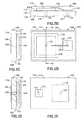
- FIGS. 1A, 1B , 1 C, 1 D, 1 E and 1 Fare respectively an isometric view, a side view, a front view, a top view, a bottom view and a cross-sectional view of a first embodiment of a packaging device in accordance with the invention.
- the cross-sectional view of FIG. 1Fis along the section line 1 F- 1 F in FIG. 1D .
- FIGS. 2A, 2B , 2 C, 2 D, 2 E and 2 Fare respectively an isometric view, a side view, a front view, a top view, a bottom view and a cross-sectional view of a first embodiment of a semiconductor device in accordance with the invention.
- the cross-sectional view of FIG. 2Fis along the section line 2 F- 2 F in FIG. 2D .
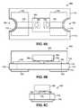
- FIGS. 3A, 3B , 3 C, 3 D, 3 E and 3 Fare respectively an isometric view, a side view, a front view, a top view, a bottom view and a cross-sectional view of a second embodiment of a packaging device in accordance with the invention.
- the cross-sectional view of FIG. 3Fis along the section line 3 F- 3 F in FIG. 3D .
- FIGS. 4A, 4B , 4 C, 4 D, 4 E and 4 Fare respectively an isometric view, a side view, a front view, a top view, a bottom view and a cross-sectional view of a second embodiment of a semiconductor device in accordance with the invention.
- the cross-sectional view of FIG. 4Fis along the section line 4 F- 4 F in FIG. 4D .
- FIGS. 5A-5Care side views illustrating a method in accordance with the invention for fabricating a packaging device for a semiconductor die.
- FIG. 5Dis a side view illustrating an optional additional process that may be included in the method illustrated in FIGS. 5A-5C .
- FIGS. 6A-6Dare side views illustrating a method in accordance with the invention for fabricating a semiconductor device.
- FIGS. 7A and 7Bare respectively a top view and a side view of a semiconductor device in accordance with another embodiment of the invention.
- FIGS. 8A, 8B and 8 Care respectively a top view and different side views of a semiconductor device in accordance with another embodiment of the invention.
- FIGS. 1A-1Fare schematic diagrams illustrating a first exemplary embodiment 100 of a packaging device for a semiconductor die in accordance with the invention.
- Packaging device 100is composed of a substrate 110 , interconnecting elements 120 and 122 , a mounting pad 130 , a bonding pad 132 and connecting pads 140 and 142 ( FIG. 1E ).
- Substrate 110is substantially planar, has opposed major surfaces 112 and 114 and defines through holes 116 and 118 that extend through the substrate between major surfaces 112 and 114 .
- Interconnecting element 120is electrically conductive and is located in through hole 116 .
- Interconnecting element 122is electrically conductive and is located in through hole 118 .
- Mounting pad 130 and bonding pad 132are electrically conductive, are separate from one another and are located on the portions of the major surface 112 of substrate 110 in which through holes 116 and 118 are respectively located.
- Connecting pads 140 and 142are electrically conductive, are separate from one another and are located on the portions of the major surface 114 of substrate 110 in which through holes 116 and 118 are respectively located.
- Mounting pad 130 and connecting pad 140are electrically connected to opposite ends of interconnecting element 120 .
- interconnecting element 120 extending through substrate 110 in through hole 116electrically connects mounting pad 130 to connecting pad 140 .
- Bonding pad 132 and connecting pad 142are electrically connected to opposite ends of interconnecting element 122 .
- interconnecting element 122 extending through substrate 110 in through hole 118electrically connects bonding pad 132 to connecting pad 142 .
- the material of substrate 110is a thermally-conductive ceramic such as alumina or beryllia.
- the material of the substratewas Kyocera.RTM. Type A440 ceramic sold by Kyocera Corp., of Kyoto, Japan. Typical dimensions of the substrate are in the range from about 0.5 mm square to about 2 mm square. Rectangular configurations are also possible.
- Alternative substrate materialsinclude semiconductors, such as silicon, and epoxy laminates, such as those used in printed-circuit boards. Other materials that have a high thermal conductivity and a low electrical conductivity can be used instead of those exemplified above.
- the coefficient of thermal expansion of the substrate material relative to that of the semiconductor die to be mounted on packaging device 100should also be considered in choosing the substrate material.
- substrate 110is part of a wafer (not shown) from which typically several hundred packaging devices 100 are fabricated by batch processing. After fabrication of the packaging devices, the wafer is singulated into individual packaging devices. Alternatively, the packaging devices may be left in wafer form after fabrication. In this case, singulation is not performed until after at least a die attach process has been performed to attach a semiconductor die to each mounting pad 130 on the wafer. In some embodiments, wafer-scale wire bonding, encapsulation and testing are also performed prior to singulation. Full electrical testing, including light output testing, may be performed on the wafer.
- interconnecting elements 120 , 122is metal or another electrically-conductive material.
- the material of the interconnecting elementsis tungsten, but any electrically-conductive material capable of forming a low-resistance electrical connection with the pads, i.e., mounting pad 130 , bonding pad 132 and connecting pads 140 , 142 , and capable of withstanding the temperature of the die-attach process may be used.
- packaging device 100may be subject to a temperature as high as about 350° C. when a gold-tin eutectic is used to attach a semiconductor die to the mounting pad 130 of the packaging device.
- Interconnecting elements 120 , 122may be located relative to mounting pad 130 and bonding pad 132 , respectively, elsewhere than the centers shown. Moreover, more than one interconnecting element may be located within either or both of the mounting pad and the bonding pad.
- the material of pads 130 , 132 , 140 , 142is metal or another electrically-conductive material. Important considerations in selecting the material of the pads are adhesion to substrate 110 , an ability to form a durable, low-resistance electrical connection with interconnecting elements 120 and 122 and an ability to withstand the temperature of the die attach process.
- the structure of the padsis a seed layer of tungsten covered with layer of nickel about 1.2 ⁇ m to about 8.9 ⁇ m thick that is in turn covered with a layer of gold about 0.75 ⁇ m thick. Other metals, alloys, conductive materials and multi-layer structures of such materials can be used.
- Packaging device 100is used to package a semiconductor die. A semiconductor device in which a semiconductor die is packaged using packaging device 100 described above will be described next.
- FIGS. 2A-2Fare schematic diagrams illustrating an exemplary embodiment 200 of a semiconductor device in accordance with the invention.
- Semiconductor device 200incorporates packaging device 100 in accordance with the invention. Elements of semiconductor device 200 that correspond to elements of packaging device 100 described above with reference to FIGS. 1A-1F are indicated using the same reference numerals and will not be described again in detail.
- Semiconductor device 200is composed of packaging device 100 described above with reference to FIGS. 1A-1F , a semiconductor die 250 , encapsulant 252 and a bonding wire 254 .
- semiconductor die 250embodies a light-emitting diode and has anode and cathode electrodes (not shown) covering at least parts of its opposed major surfaces.
- Semiconductor die 250is mounted on packaging device 100 with the metallization on its bottom major surface attached to mounting pad 130 .
- Encapsulant 252covers the semiconductor die and the part of the major surface 112 of substrate 100 where mounting pad 130 and bonding pad 132 are located.
- Bonding wire 254extends between a bonding pad located on the top major surface of semiconductor die 250 and bonding pad 132 .
- the bonding pad on the top major surface of semiconductor die 250is typically part of or connected to the anode electrode of the light-emitting diode.
- the metallization on the bottom major surface of semiconductor die 250typically constitutes the cathode electrode of the light-emitting diode.
- the anode electrode of semiconductor die 250is electrically connected to connecting pad 142 by bonding wire 254 , bonding pad 132 and interconnecting element 122 , and the cathode electrode of semiconductor die 250 is electrically connected to connecting pad 140 by mounting pad 130 and interconnecting element 120 .
- Encapsulant 252has a thickness greater than the maximum height of bonding wire 254 above major surface 112 .
- the encapsulantis transparent to enable semiconductor device 200 to emit the light generated by semiconductor die 250 .
- Semiconductor die 250is composed of one or more layers (not shown) of any semiconductor material composed of elements from Groups II, III, IV, V and VI of the periodic table in binary, ternary, quaternary or other form.
- Semiconductor die 250may additionally include a non-semiconductor substrate material, such as sapphire, metal electrode materials and dielectric insulating materials, as is known in the art.
- semiconductor die 250is composed of a substrate of silicon carbide that supports one or more layers of (indium) gallium nitride. Such a light-emitting diode generates light in a wavelength range extending from ultra-violet to green.
- the bottom major surface (not shown) of the substrate remote from the layers of (indium) gallium nitrideis coated with a metallization layer of a gold-tin alloy.
- a gold-tin eutecticattaches the semiconductor die to mounting pad 130 , as described above, to provide a mechanical and electrical connection between the semiconductor die and the mounting pad.
- the material of bonding wire 254is gold.
- a process known in the art as low-loop wire bondingis used to connect the bonding wire between the anode electrode of semiconductor die 250 and bonding pad 132 . Using low-loop wire bonding minimizes the maximum height of the bonding wire above substrate 110 , and, therefore, reduces the overall height of semiconductor device 200 .
- Other processes for providing an electrical connection between a bonding pad on a semiconductor die and a bonding pad on a packaging deviceare known in the art and may be used instead, especially in applications in which device height is a less important consideration.
- encapsulant 252is clear epoxy.
- Alternative encapsulant materialsinclude silicone.
- Embodiments of semiconductor device 200 that neither emit nor detect lightcan use an opaque encapsulant.
- semiconductor die 250is embodied as a light-emitting diode.
- Semiconductor die 250may alternatively embody another type of diode without modification to packaging device 100 .
- Versions of packaging device 100may be used to package semiconductor die other than those that embody such electrical components as diodes that have only two electrodes.
- Versions of packaging device 100may be used to package semiconductor die that embody such electronic circuit elements as transistors and integrated circuits that have more than two electrodes.
- Such versions of packaging device 100have a number of bonding pads, interconnecting elements and connecting pads corresponding to the number of bonding pads located on the top major surface of the semiconductor die.
- a version of packaging device 100 for packaging a semiconductor diethat embodies a transistor having collector, base and emitter electrodes, and in which the substrate metallization provides the collector electrode, has two bonding pads, two interconnecting elements and two connecting pads. Wire bonds connect the emitter bonding pad on the semiconductor die to one of the bonding pads on the packaging device and the base bonding pad on the semiconductor die to the other of the bonding pads on the packaging device.
- the connecting pads, e.g., connecting pads 140 and 142 , of embodiments of packaging device 100 having multiple connecting padsmay be arranged to conform with an industry standard pad layout to facilitate printed circuit layout.
- the interconnecting elementsmay be offset from the centers of the respective mounting pads, bonding pads and connecting pads to allow the connecting pad layout to conform with such a standard pad layout.
- one or more of the mounting pad, bonding pads and connecting padsmay have a shape that differs from the regular shapes illustrated. Some irregular shapes include two main regions electrically connected by a narrow track. For example, an irregularly-shaped bonding pad includes a region to which the bonding wire is attached, a region connected to the interconnecting element and a narrow track interconnecting the two regions.
- packaging devicemay accommodate two or more semiconductor die.
- mounting pad 130is sized large enough to accommodate the two or more semiconductor die.
- such versionsinclude sufficient bonding pads, interconnecting elements and connecting pads to make the required number of electrical connections to the semiconductor die.
- the packaging devicemay include two or more mounting pads. The mounting pads may be electrically connected to one another and thence to a common interconnecting element and connecting pad. Alternatively, each mounting pad may be electrically connected to a corresponding connecting pad by a respective interconnecting element.
- Semiconductor device 200is used by mounting it on a printed circuit board or other substrate using conventional surface-mount techniques or other techniques known in the art. Semiconductor device 200 is placed on a surface of the printed circuit board with connecting pads 140 and 142 aligned with respective pads on the printed circuit board. The printed circuit board is then passed across a solder wave to form a solder joint between connecting pads 140 and 142 and the respective pads on the printed circuit board.
- semiconductor device 200may be affixed to a printed circuit board by a process known as infra-red reflow soldering in which a pattern of solder is applied to the printed circuit board using a stencil, semiconductor device 200 and, optionally, other components are loaded onto the printed circuit board and the printed circuit board assembly is irradiated with infra-red light to heat and reflow the solder.
- infra-red reflow solderingin which a pattern of solder is applied to the printed circuit board using a stencil, semiconductor device 200 and, optionally, other components are loaded onto the printed circuit board and the printed circuit board assembly is irradiated with infra-red light to heat and reflow the solder.
- Other processes for attaching electronic components to printed circuit boardsare known in the art and may alternatively be used.
- Packaging device 100 and semiconductor device 200may additionally include adhesive regions on the major surface 114 of substrate 110 external to connecting pads 140 and 142 to hold the semiconductor device in place on the printed circuit board during soldering.
- packaging device 100 and encapsulant 252collectively have a volume that is only about 15 times the volume of semiconductor die 250 .
- packaging device 100is well suited for use in high packing density applications.
- packaging device 100is fabricated from materials capable of withstanding the high temperatures involved in a die attach process that uses a gold-tin eutectic. Accordingly, packaging device 100 is well suited for packaging semiconductor die, such as the die of certain light-emitting devices, that require a die attach process that uses a gold-tin eutectic.
- FIGS. 3A-3Fare schematic drawings showing a second embodiment 300 of a packaging device in accordance with the invention.
- Packaging device 300takes the form of a submount that enables semiconductor die that are mounted using a gold-tin eutectic or other high-temperature die attach process to be mounted in conventional semiconductor device packages that are incapable of withstanding such high temperatures.
- packaging device 300 with a semiconductor die mounted thereoncan be mounted in a conventional semiconductor device package as if it were a conventional semiconductor die. This allows conventional die attach, wire bond and encapsulation processes to be used to assemble the final semiconductor device that incorporates the submount.
- FIGS. 3A-3Fare schematic diagrams illustrating a second exemplary embodiment 300 of a packaging device for a semiconductor die in accordance with the invention.
- Packaging device 300takes the form of a submount for a semiconductor die.
- Packaging device 300is composed of a substrate 310 , an interconnecting element 320 , a mounting pad 330 and a connecting pad 340 ( FIG. 3E ).
- Substrate 310is substantially planar, has opposed major surfaces 312 and 314 and defines a through hole 316 that extends through the substrate between major surfaces 312 and 314 .
- Interconnecting element 320is electrically conductive and is located in through hole 316 .
- Mounting pad 330is electrically conductive and is located on a portion of the major surface 312 of substrate 310 in which through hole 316 is located. Alternatively, mounting pad 330 may cover major surface 312 .
- Connecting pad 340is electrically conductive and is located on a portion of the major surface 314 of the substrate in which through hole 316 is located. Alternatively, connecting pad 340 may cover major surface 314 .
- Mounting pad 330 and connecting pad 340are electrically connected to opposite ends of interconnecting element 320 .
- interconnecting element 320extending through the substrate in through hole 316 electrically connects mounting pad 330 to connecting pad 340 .
- substrate 310Materials and other details of substrate 310 , interconnecting element 320 , mounting pad 330 and connecting pad 340 are the same as those of substrate 110 , interconnecting element 120 , mounting pad 130 and connecting pad 140 , respectively, of packaging device 100 described above with reference to FIGS. 1A-1F and will therefore not be described again here.
- a semiconductor device in which a semiconductor die is packaged using packaging device 300 described abovewill be described next.
- FIGS. 4A-4Fare schematic diagrams illustrating an exemplary embodiment 400 of a semiconductor device in accordance with the invention.
- Semiconductor device 400incorporates packaging device 300 in accordance with the invention. Elements of semiconductor device 400 that correspond to elements of semiconductor device 200 described above with reference to FIGS. 2A-2F and of packaging device 300 described above with reference to FIGS. 3A-3F are indicated using the same reference numerals and will not be described again in detail.
- Semiconductor device 400is composed of a semiconductor die 250 mounted on packaging device 300 described above with reference to FIGS. 3A-3F .
- semiconductor die 250embodies a light-emitting diode and has anode and cathode electrodes (not shown) covering at least parts of its opposed major surfaces.
- semiconductor die 250is mounted on packaging device 300 with the metallization on its bottom major surface attached to mounting pad 330 .
- the metallization on the bottom major surface of semiconductor die 250typically constitutes the cathode electrode of the light-emitting diode.
- the cathode electrode of semiconductor die 250is electrically connected to connecting pad 340 by mounting pad 330 and interconnecting element 320 .
- the top major surface of semiconductor die 250typically includes a bonding pad that is typically part of or connected to the anode electrode of the light-emitting diode. This bonding pad remains exposed for later connection to the conventional semiconductor packaging device in which semiconductor device 400 will later be mounted.
- Semiconductor device 400is used by mounting it on a conventional semiconductor packaging device (not shown), such as the lead frame of a plastic package. Specifically, semiconductor device 400 is mounted on the lead frame with connecting pad 340 attached to a conductive mounting surface of the lead frame. Connecting pad 340 is attached to the mounting surface of the lead frame using a low-temperature die attach process, such as one that uses silver epoxy. Thus, semiconductor device 400 is compatible with conventional semiconductor device assembly processes. One or more bonding wires (not shown) are connected between bonding pads on the exposed major surface of semiconductor die 250 and the bonding pads of the lead frame. The lead frame with semiconductor device 400 mounted thereon is then encapsulated to complete the fabrication of the semiconductor device. Semiconductor device 400 may be mounted on or in conventional semiconductor packaging devices other that the lead frame based packaging device just exemplified.
- Semiconductor device 400is also suitable for attaching directly to a printed circuit board.
- a conventional die attach processcan be used to attach connecting pad 340 directly to a suitably-sized pad on the printed circuit board. Such a die attach process does not subject the printed circuit board to the high temperatures that were used to attach semiconductor die 250 to the mounting pad 330 of packaging device 300 .
- a substrateis provided.
- the substrateis substantially planar, has opposed major surfaces, and includes a through hole extending between the major surfaces.
- the through holeis filled with a conductive interconnecting element.
- a conductive mounting pad and a conductive connecting padare formed on different ones of the major surfaces in electrical contact with the conductive interconnecting element.
- FIGS. 5A-5Cshow a highly simplified example of the method in which two packaging devices similar to packaging device 100 described above with reference to FIGS. 1A-1F are fabricated in a wafer.
- hundreds of packaging devicesare typically fabricated simultaneously in a single wafer of substrate material.
- FIG. 5Ashows a wafer 510 of substrate material.
- a portion of the waferconstitutes the substrate of each of the packaging devices that will be fabricated in the wafer.
- Wafer 510has opposed major surfaces 512 and 514 . Portions of major surfaces 512 and 514 constitute the major surfaces of each of the packaging devices that will be fabricated in the wafer.
- the material of wafer 510is one of the substrate materials described above.
- wafer 510Defined in wafer 510 is at least one through hole for each of the packaging devices that will be fabricated in the wafer.
- a packaging device similar to packaging device 300 described above with reference to FIGS. 3A-3Fhas one through hole per packaging device.
- each packaging deviceis similar to packaging device 100 described above with reference to FIGS. 1A-1F and has two through holes per packaging device. Through holes 516 and 518 of one of the packaging devices and through holes 517 and 519 of the other of the packaging devices are shown.
- through holes 516 - 519are formed by punching.
- the through holesmay alternatively be formed by drilling or laser ablation. Many other ways suitable for forming holes having a diameter in a range from about 100 ⁇ m to about 2 mm are known in the art and may be used instead.
- FIG. 5Bshows interconnecting elements 520 - 523 being introduced into through holes 516 - 519 , respectively, to fill the through holes.
- Interconnecting elements 520 - 523are slugs of conductive material having a diameter smaller than the diameter of the through holes and a length larger than the thickness of wafer 510 .
- the material of the interconnecting elementsis tungsten.
- a squeezing processis used to fill the through holes with the interconnecting elements. The squeezing process introduces the interconnecting elements into the through holes and then reduces the length and increases the diameter of the interconnecting elements.
- the squeezing processleaves the ends of the interconnecting elements approximately flush with respective major surfaces 512 and 514 , and the interconnecting elements retained in the through holes by friction.
- An adhesivemay additionally or alternatively be used to retain the interconnecting elements in the through holes.
- the through holemay be filled with the interconnecting element in other ways.
- through-hole platingmay be used.
- screen printing or metal depositionare used.
- a through holewill be regarded as having been filled with an interconnecting element even when the interconnecting element occupies only part of the volume of the through hole.
- FIG. 5Cshows mounting pad 530 and connecting pad 540 formed on major surfaces 512 and 514 , respectively, of wafer 510 in electrical contact with the opposite ends of interconnecting element 520 .
- FIG. 5Cadditionally shows mounting pad 531 and connecting pad 541 formed on major surfaces 512 and 514 , respectively, in electrical contact with interconnecting element 521 , bonding pad 532 and connecting pad 542 formed on major surfaces 512 and 514 , respectively, in electrical contact with interconnecting element 522 , and bonding pad 533 and connecting pad 543 formed on major surfaces 512 and 514 , respectively, in electrical contact with interconnecting element 523 .
- Conductive pads 530 - 533 and 540 - 543are formed on wafer 510 by electro less plating using a screen printed mask.
- a photo maskmay alternatively be used. Examples of other selective processes that may be used to form pads 530 - 533 and 540 - 543 are electroplating, screen printing and metal deposition.
- major surfaces 512 and 514are each initially covered with a layer of metal using a cladding process.
- the layer of metalmay take the form a metal foil pressed into contact with the respective major surface to cause the foil to adhere to the wafer.
- An adhesivemay be used to increase adhesion. Portions of the layer of metal are then selectively removed to define pads 530 - 533 and 540 - 543 .
- a mask and etch processmay be used to perform the selective removal.
- Packaging devices in accordance with the inventionare typically supplied to users in the wafer state shown in FIG. 5C so that they can be used in wafer-scale assembly processes. However, the packaging devices can alternatively be supplied singly.
- FIG. 5Dshows an optional additional element of the above-described fabrication method in which wafer 510 is singulated into individual packaging devices 100 and 101 . Singulation may be performed by sawing, scribing and breaking or by another singulation process.
- through holes 516 - 519are formed in wafer 510 ( FIG. 5A ), the through holes are filled with interconnecting elements 520 - 523 ( FIG. 5B ) and regions of tungsten, each of which constitutes a seed layer for one of the conductive pads 530 - 533 and 540 - 543 , are screen printed on the wafer with the wafer in its “green”, i.e., unfired state. The wafer is then fired. After the wafer has been fired, an electroless plating process is performed to deposit one or more additional layers of metal to complete the formation of conductive pads 530 - 533 and 540 - 543 ( FIG. 5C ).
- a method in accordance with the invention for fabricating a semiconductor device using the wafer-scale device packages shown in FIG. 5Cwill now be described.
- the methodcan be used to fabricate the semiconductor devices described above with reference to FIGS. 2A-2F .
- Portions of the methodcan be used to fabricate the semiconductor devices illustrated in FIGS. 4A-4F .
- a semiconductor dieis mounted on the mounting pad of the packaging device, a bonding wire is connected between the semiconductor die and the bonding pad of the packaging device, and the semiconductor die and at least a portion of the major surface of the packaging device on which the mounting pad is located are encapsulated.
- FIGS. 6A-6Dshow a highly simplified example in which two semiconductor devices similar to semiconductor device 200 described above with reference to FIGS. 2A-2F are fabricated. As noted above, hundreds of semiconductor devices are typically fabricated simultaneously on a single wafer.
- FIG. 6Ashows a wafer-scale array 600 of packaging devices supplied in wafer-scale form on wafer 510 .
- Semiconductor device 250is mounted on mounting pad 530 and a semiconductor device 251 is mounted on mounting pad 531 .
- a semiconductor die having a gold-tin metallization on its bottom major surfaceis placed on each mounting pad 530 , 531 on wafer 510 .
- the waferis then heated to a temperature in the range from about 280° C. to about 350° C. for a time in the range from about one second to about 60 seconds.
- the gold-tin eutectic that formsattaches the semiconductor die to the respective mounting pad when the wafer is allowed to cool.
- die attach processesincluding die attach processes that require substantially lower peak temperatures, are known in the art and may be used instead of the die attach process just described. Not all die attach processes are suitable for use with all die metallizations, however.
- FIG. 6Bshows a bonding wire 254 connected between a bonding pad (not shown) on the exposed major surface of semiconductor die 250 and bonding pad 532 and a bonding wire 255 connected between a bonding pad (not shown) on the exposed major surface of semiconductor die 251 and bonding pad 533 .
- low loop wire bondingis used to connect bonding wires 254 , 255 between semiconductor die 250 , 251 and bonding pads 532 , 533 .
- Other ways to electrically connect a bonding pad located on the exposed surface of a semiconductor die to a bonding pad similar to bonding pads 532 , 533are known the art and can alternatively be used.
- FIG. 6Cshows semiconductor die 250 and a portion of major surface 512 on which mounting pad 530 is located encapsulated by encapsulation 252 , and semiconductor die 251 and a portion of major surface 512 on which mounting pad 531 is located encapsulated by encapsulation 253 .
- the encapsulantis clear epoxy. Silicone is another suitable encapsulant. Other encapsulants are known in the art and may be used where appropriate. In an embodiment, the encapsulant was applied by transfer molding. Other application processes are known in the art and may be used where appropriate. Examples of other suitable application processes include injection molding, casting and dam and fill.
- FIG. 6Dshows wafer 510 after it has been singulated into individual semiconductor devices 200 and 201 .
- Singulationmay be performed by sawing, scribing and breaking or by another suitable singulation process.
- the semiconductor devices fabricated on wafer 510may be electrically tested before the wafer is singulated. The ability to test the semiconductor devices at the wafer scale level substantially reduces the cost of testing.
- FIGS. 6B and 6Care omitted when the method illustrated in FIGS. 6A-6D is used to fabricate a submount semiconductor device similar to that described above with reference to FIGS. 4A-4F .
- FIGS. 7A and 7Ba semiconductor device 700 in accordance with another embodiment of the invention is shown.
- FIG. 7Ais a top view of the semiconductor device 700
- FIG. 7Bis a side view of the semiconductor device 700 .
- the semiconductor device 700is similar to the semiconductor device 200 .
- the semiconductor device 700does not use any bonding wire, such as the bonding wire 254 of the semiconductor device 200 .
- the semiconductor device 700includes a substrate 710 , interconnecting elements 720 and 722 , bonding pads 730 and 732 , connecting pads 740 and 742 , and a semiconductor die 750 .
- the substrate 710is identical to the substrate 110 of the semiconductor device 200 .
- the interconnecting elements 720 and 722are identical to the interconnecting elements 120 and 122 of the semiconductor device 200 .
- the interconnecting elements 720 and 722are located in through holes 716 and 718 of the substrate 710 .
- the interconnecting elements 720 and 722can be made of the same material as the interconnecting elements 120 and 122 of the semiconductor device 200 .
- the bonding pads 730 and 732are similar to the mounting pad 130 and the bonding pad 132 of the semiconductor device 200 .
- the bonding pads 730 and 732are located on an upper major surface 712 of the substrate 710 .
- the shapes of the bonding pads 730 and 732differ from those of the mounting pad 130 and the bonding pad 132 of the semiconductor device 200 .
- the bonding pads 730 and 732are rectangular in shape.
- the bonding pads 730 and 732may be configured in other shapes.
- the connecting pads 740 and 742are similar to the connecting pads 140 and 142 of the semiconductor device 200 .
- the connecting pad 740 and 742are located on a lower major surface 714 of the substrate 710 .
- the semiconductor die 750is a die with bond pads 760 and 762 on a lower major surface of the die, which is the surface that faces the substrate 710 when the die is mounted on the substrate.
- the semiconductor die 750is a light emitting diode (LED) die.
- the bond pads 760 and 762are connected to the anode and the cathode of the LED die, which are located on the bottom major surface of the LED die.
- the bond pads 760 and 762can be considered as the anode and cathode bond pads, respectively, or vice versa.
- the semiconductor die 750may be a different type of a light emitting semiconductor die, such as a laser diode.
- the semiconductor die 750is mounted on the substrate 710 using flip chip technology. Specifically, the semiconductor die 750 is mounted on the bonding pads 730 and 732 such that the bond pad 760 is attached to the bonding pad 730 and the bond pad 762 is attached to the bonding pad 732 . As an example, the bond pads 760 and 762 may be attached to the bonding pads 730 and 732 , respectively, using solder bumps or other electrically conductive and adhesive material.
- the bond pad 760 of the semiconductor die 750is electrically connected to the connecting pad 740 via the bonding pad 730 and the interconnecting element 720
- the bond pad 762 of the semiconductor die 750is electrically connected to the connecting pad 742 via the bonding pad 732 and the interconnecting element 722 .
- no bonding wireis used to electrically connect the semiconductor die 750 to any of the bonding pads 730 and 732 .
- the semiconductor die 750 of the semiconductor device 700may be encapsulated by an encapsulant 752 (only illustrated in FIG. 7B ), which can be identical to the encapsulant 152 of the semiconductor device 200 .
- FIGS. 8A, 8B and 8 Ca semiconductor device 800 in accordance with another embodiment of the invention is shown.
- FIG. 8Ais a top view of the semiconductor device 800
- FIGS. 8B and 8Care different side views of the semiconductor device 800 .
- the semiconductor device 800is similar to the semiconductor device 700 .
- the reference numbers of FIGS. 7A and 7Bwill be used in FIGS. 8A-8C to indicate similar elements.
- the semiconductor device 800includes the substrate 710 , the bonding pads 730 and 732 , the connecting pads 740 and 742 , and the semiconductor die 750 .
- the semiconductor device 800does not include the interconnecting elements 720 and 722 , which electrically connect the bonding pads 730 and 732 to the connecting pads 740 and 742 , respectively, through the substrate 710 via the through holes 716 and 718 .
- the bonding pads 730 and 732are electrically connected to the connecting pads 740 and 742 via edge interconnecting elements 770 and 772 , as illustrated in FIG. 8C , which is a side view of the semiconductor device 800 showing the edge interconnecting element 770 .
- the edge interconnecting elements 770 and 772are located on sidewalls of the substrate 710 . In the illustrated embodiment, the edge interconnecting elements 770 and 772 are located on opposed sidewalls of the substrate 710 . However, in other embodiments, the edge interconnecting elements 770 and 772 may be located on different sidewalls of the substrate 710 , or even on the same sidewall.
- the edge interconnecting elements 770 and 772can be made of the same material as the interconnecting elements 120 and 122 of the semiconductor device 200 .
- the edge interconnecting elements 770 and 772are attached to their respective sidewalls within partial cylindrical depressions 780 and 782 , respectively.
- the partial cylindrical depressions 780 and 782are created by forming circular holes through the substrate 710 connecting the upper and lower major surfaces 712 and 714 of the substrate 710 .
- the circular holesare then coated or filled with appropriate material for the edge interconnecting elements 770 and 772 .
- the semiconductor device 800is separated from other semiconductor devices on a wafer, these circular holes are cut in half, which forms the partial cylindrical depressions 780 and 782 on the sidewalls of the substrate 710 , as well as the edge interconnecting elements 770 and 772 within the partial cylindrical depressions 780 and 782 .
- the semiconductor device 800does not use interconnecting elements that extend through the substrate 710 to electrically connect the bonding pads 730 and 732 to the connecting pads 740 and 742 .
- the semiconductor die 750 of the semiconductor device 800may be encapsulated by an encapsulant 752 (only illustrated in FIG. 8 B), which can be identical to the encapsulant 152 of the semiconductor device 200 .
- Edge interconnecting elementssuch as the edge interconnecting elements 770 and 772 of the semiconductor device 800 , may also be used in other semiconductor devices to electrically connect pads on opposed substrate surfaces of the devices.
- edge interconnecting elementsmay be used in the semiconductor device 200 to electrically connect the mounting pad 130 and the bonding pad 132 to the connecting pads 140 and 142 , respectively.
- the interconnecting elements 120 and 122 located in the through holes 116 and 118 , respectively,will no longer be needed to electrically connect the mounting pad 130 and the bonding pad 132 to the connecting pads 140 and 142 , respectively.
Landscapes
- Led Device Packages (AREA)
Abstract
Description
- This application is a continuation-in-part of U.S. patent application Ser. No. 10/608,605, filed Jun. 27, 2003, which is related to U.S. patent application Ser. No. 10/608,606, filed Jun. 27, 2003. Both disclosures are specifically incorporated herein by reference.
- Many types of conventional semiconductor device are composed of a semiconductor die mounted in a packaging device. One type of packaging device widely used in the industry includes a metal lead frame. A metallization layer of aluminum located on the bottom surface of the semiconductor die is bonded to a conductive surface that forms part of the lead frame to attach and electrically connect the die to the lead frame. Additionally, electrical connections are made between bonding pads on the top surface of the die and other leads of the lead frame to provide additional electrical connections to the die. The lead frame and semiconductor die are then encapsulated to complete the semiconductor device. The packaging device protects the semiconductor die and provides electrical and mechanical connections to the die that are compatible with conventional printed circuit board assembly processes.
- In such conventional semiconductor devices, the bottom surface of the die is typically bonded to the conductive surface of the lead frame using a silver epoxy adhesive that cures at a relatively low temperature, typically about 120° C. The curing temperature of the silver epoxy adhesive is compatible with the other materials of the packaging device.
- The volume of the packaging device used in such conventional semiconductor devices, i.e., the lead frame and the encapsulant, is typically many times that of the semiconductor die. This makes such conventional semiconductor devices unsuitable for use in applications in which a high packing density is required. A high packing density allows miniaturization and other benefits. Therefore, what is needed is a semiconductor packaging device that is comparable in volume with the semiconductor die and that is compatible with conventional printed circuit board assembly processes.
- Recently, semiconductor die having a substrate surface metallization layer of a gold-tin alloy (80% Au:20% Sn approximately) have been introduced in light-emitting devices. Such semiconductor die typically have a substrate of sapphire, silicon carbide or a Group ITT-V semiconductor material, such as gallium arsenide. Semiconductor devices having substrates of the first two substrate materials have layers of Group ITT-V semiconductor materials, such as gallium nitride, deposited on their substrates. The die attach process for such semiconductor die uses a gold-tin eutectic, which has a melting point of about 280° C. Temperatures as high as about 350° C. can be encountered in the die attach process for such die. Such high temperatures are incompatible with the materials of many conventional packaging devices. Thus, what is also needed is a packaging device for semiconductor die that use a high-temperature die attach process.
- Many printed circuit assembly processes and assembly equipment require the use of standard semiconductor device packages. Modifying such processes to use a new semiconductor device package can be expensive and can interrupt production. Therefore, what is additionally needed is a way to mount a semiconductor die that requires a high-temperature die attach process in a conventional packaging device.
- A semiconductor device includes a light emitting semiconductor die mounted on at least one of first and second electrically conductive bonding pads, which are located on a first major surface of a substrate of the device. The light emitting semiconductor die has an anode and a cathode, which are electrically connected to the first and second electrically conductive bonding pads. The semiconductor device further includes first and second electrically conductive connecting pads, which are located on a second major surface of the substrate. The first and second electrically conductive bonding pads are electrically connected to the first and second electrically conductive connecting pads via first and second electrically conductive interconnecting elements.
- A semiconductor device in accordance with an embodiment of the invention includes a substantially planar substrate, first and second electrically conductive bonding pads, a light emitting semiconductor die, first and second electrically conductive connecting pads, and first and second electrically conductive interconnecting elements. The substantially planar substrate has first and second major surfaces. The first and second major surfaces are opposed surfaces. The first and second electrically conductive bonding pads are located on the first major surface. The light emitting semiconductor die has at least one of an anode and a cathode on a bottom major surface of the light emitting semiconductor die. The anode and the cathode of the light emitting semiconductor die are electrically connected to the first and second electrically conductive bonding pads. The semiconductor light emitting die is mounted on at least the first electrically conductive bonding pad such that one of the anode and the cathode on the bottom major surface of the light emitting semiconductor die is electrically connected to the first electrically conductive bonding pad. The first and second electrically conductive connecting pads are located on the second major surface. The first electrically conductive interconnecting element is electrically connected to the first electrically conductive bonding pad and the first electrically conductive connecting pad. The second electrically conductive interconnecting element is electrically connected to the second electrically conductive bonding pad and the second electrically conductive connecting pad. In an embodiment, at least one of the first and second electrically conductive interconnecting elements is located on at least one sidewall of the substantially planar substrate.
- A semiconductor device in accordance with another embodiment of the invention includes a substantially planar substrate, first and second electrically conductive bonding pads, a light emitting semiconductor die, first and second electrically conductive connecting pads, and first and second electrically conductive interconnecting elements. The substantially planar substrate has first and second major surfaces. The first and second major surfaces are opposed surfaces. The first and second electrically conductive bonding pads are located on the first major surface. The light emitting semiconductor die has an anode and a cathode on a bottom major surface of the light emitting semiconductor die. The semiconductor light emitting die is mounted on the first and second electrically conductive bonding pads such that the anode of the light emitting semiconductor die is electrically connected to the first electrically conductive bonding pad and the cathode of the light emitting semiconductor die is electrically connected to the second electrically conductive bonding pad. The first and second electrically conductive connecting pads are located on the second major surface. The first electrically conductive interconnecting element is electrically connected to the first electrically conductive bonding pad and the first electrically conductive connecting pad. The second electrically conductive interconnecting element is electrically connected to the second electrically conductive bonding pad and the second electrically conductive connecting pad
- Other aspects and advantages of the present invention will become apparent from the following detailed description, taken in conjunction with the accompanying drawings, illustrated by way of example of the principles of the invention.
FIGS. 1A, 1B ,1C,1D,1E and1F are respectively an isometric view, a side view, a front view, a top view, a bottom view and a cross-sectional view of a first embodiment of a packaging device in accordance with the invention. The cross-sectional view ofFIG. 1F is along thesection line 1F-1F inFIG. 1D .FIGS. 2A, 2B ,2C,2D,2E and2F are respectively an isometric view, a side view, a front view, a top view, a bottom view and a cross-sectional view of a first embodiment of a semiconductor device in accordance with the invention. The cross-sectional view ofFIG. 2F is along thesection line 2F-2F inFIG. 2D .FIGS. 3A, 3B ,3C,3D,3E and3F are respectively an isometric view, a side view, a front view, a top view, a bottom view and a cross-sectional view of a second embodiment of a packaging device in accordance with the invention. The cross-sectional view ofFIG. 3F is along thesection line 3F-3F inFIG. 3D .FIGS. 4A, 4B ,4C,4D,4E and4F are respectively an isometric view, a side view, a front view, a top view, a bottom view and a cross-sectional view of a second embodiment of a semiconductor device in accordance with the invention. The cross-sectional view ofFIG. 4F is along thesection line 4F-4F inFIG. 4D .FIGS. 5A-5C are side views illustrating a method in accordance with the invention for fabricating a packaging device for a semiconductor die.FIG. 5D is a side view illustrating an optional additional process that may be included in the method illustrated inFIGS. 5A-5C .FIGS. 6A-6D are side views illustrating a method in accordance with the invention for fabricating a semiconductor device.FIGS. 7A and 7B are respectively a top view and a side view of a semiconductor device in accordance with another embodiment of the invention.FIGS. 8A, 8B and8C are respectively a top view and different side views of a semiconductor device in accordance with another embodiment of the invention.FIGS. 1A-1F are schematic diagrams illustrating a firstexemplary embodiment 100 of a packaging device for a semiconductor die in accordance with the invention.Packaging device 100 is composed of asubstrate 110, interconnectingelements pad 130, abonding pad 132 and connectingpads 140 and142 (FIG. 1E ).Substrate 110 is substantially planar, has opposedmajor surfaces holes major surfaces element 120 is electrically conductive and is located in throughhole 116. Interconnectingelement 122 is electrically conductive and is located in throughhole 118. Mountingpad 130 andbonding pad 132 are electrically conductive, are separate from one another and are located on the portions of themajor surface 112 ofsubstrate 110 in which throughholes Connecting pads major surface 114 ofsubstrate 110 in which throughholes - Mounting
pad 130 and connectingpad 140 are electrically connected to opposite ends of interconnectingelement 120. Thus, interconnectingelement 120 extending throughsubstrate 110 in throughhole 116 electrically connects mountingpad 130 to connectingpad 140.Bonding pad 132 and connectingpad 142 are electrically connected to opposite ends of interconnectingelement 122. Thus, interconnectingelement 122 extending throughsubstrate 110 in throughhole 118 electrically connectsbonding pad 132 to connectingpad 142. - The material of
substrate 110 is a thermally-conductive ceramic such as alumina or beryllia. In an embodiment, the material of the substrate was Kyocera.RTM. Type A440 ceramic sold by Kyocera Corp., of Kyoto, Japan. Typical dimensions of the substrate are in the range from about 0.5 mm square to about 2 mm square. Rectangular configurations are also possible. Alternative substrate materials include semiconductors, such as silicon, and epoxy laminates, such as those used in printed-circuit boards. Other materials that have a high thermal conductivity and a low electrical conductivity can be used instead of those exemplified above. The coefficient of thermal expansion of the substrate material relative to that of the semiconductor die to be mounted onpackaging device 100 should also be considered in choosing the substrate material. - As will be described in more detail below,
substrate 110 is part of a wafer (not shown) from which typically several hundredpackaging devices 100 are fabricated by batch processing. After fabrication of the packaging devices, the wafer is singulated into individual packaging devices. Alternatively, the packaging devices may be left in wafer form after fabrication. In this case, singulation is not performed until after at least a die attach process has been performed to attach a semiconductor die to each mountingpad 130 on the wafer. In some embodiments, wafer-scale wire bonding, encapsulation and testing are also performed prior to singulation. Full electrical testing, including light output testing, may be performed on the wafer. - The material of interconnecting
elements pad 130,bonding pad 132 and connectingpads packaging device 100 may be subject to a temperature as high as about 350° C. when a gold-tin eutectic is used to attach a semiconductor die to themounting pad 130 of the packaging device. Interconnectingelements pad 130 andbonding pad 132, respectively, elsewhere than the centers shown. Moreover, more than one interconnecting element may be located within either or both of the mounting pad and the bonding pad. - The material of
pads substrate 110, an ability to form a durable, low-resistance electrical connection with interconnectingelements Packaging device 100 is used to package a semiconductor die. A semiconductor device in which a semiconductor die is packaged usingpackaging device 100 described above will be described next.FIGS. 2A-2F are schematic diagrams illustrating anexemplary embodiment 200 of a semiconductor device in accordance with the invention.Semiconductor device 200 incorporatespackaging device 100 in accordance with the invention. Elements ofsemiconductor device 200 that correspond to elements ofpackaging device 100 described above with reference toFIGS. 1A-1F are indicated using the same reference numerals and will not be described again in detail.Semiconductor device 200 is composed ofpackaging device 100 described above with reference toFIGS. 1A-1F , asemiconductor die 250,encapsulant 252 and abonding wire 254. In the example shown, semiconductor die250 embodies a light-emitting diode and has anode and cathode electrodes (not shown) covering at least parts of its opposed major surfaces. Semiconductor die250 is mounted onpackaging device 100 with the metallization on its bottom major surface attached to mountingpad 130.Encapsulant 252 covers the semiconductor die and the part of themajor surface 112 ofsubstrate 100 where mountingpad 130 andbonding pad 132 are located.Bonding wire 254 extends between a bonding pad located on the top major surface of semiconductor die250 andbonding pad 132.- The bonding pad on the top major surface of semiconductor die250 is typically part of or connected to the anode electrode of the light-emitting diode. The metallization on the bottom major surface of semiconductor die250 typically constitutes the cathode electrode of the light-emitting diode. Thus, the anode electrode of semiconductor die250 is electrically connected to connecting
pad 142 bybonding wire 254,bonding pad 132 and interconnectingelement 122, and the cathode electrode of semiconductor die250 is electrically connected to connectingpad 140 by mountingpad 130 and interconnectingelement 120. Encapsulant 252 has a thickness greater than the maximum height ofbonding wire 254 abovemajor surface 112. In the example shown, the encapsulant is transparent to enablesemiconductor device 200 to emit the light generated by semiconductor die250.- Semiconductor die250 is composed of one or more layers (not shown) of any semiconductor material composed of elements from Groups II, III, IV, V and VI of the periodic table in binary, ternary, quaternary or other form. Semiconductor die250 may additionally include a non-semiconductor substrate material, such as sapphire, metal electrode materials and dielectric insulating materials, as is known in the art.
- In an embodiment of the above-described example in which semiconductor die250 embodies a light-emitting diode, semiconductor die250 is composed of a substrate of silicon carbide that supports one or more layers of (indium) gallium nitride. Such a light-emitting diode generates light in a wavelength range extending from ultra-violet to green. The bottom major surface (not shown) of the substrate remote from the layers of (indium) gallium nitride is coated with a metallization layer of a gold-tin alloy. A gold-tin eutectic attaches the semiconductor die to mounting
pad 130, as described above, to provide a mechanical and electrical connection between the semiconductor die and the mounting pad. - The material of
bonding wire 254 is gold. A process known in the art as low-loop wire bonding is used to connect the bonding wire between the anode electrode of semiconductor die250 andbonding pad 132. Using low-loop wire bonding minimizes the maximum height of the bonding wire abovesubstrate 110, and, therefore, reduces the overall height ofsemiconductor device 200. Other processes for providing an electrical connection between a bonding pad on a semiconductor die and a bonding pad on a packaging device are known in the art and may be used instead, especially in applications in which device height is a less important consideration. - The material of
encapsulant 252 is clear epoxy. Alternative encapsulant materials include silicone. Embodiments ofsemiconductor device 200 that neither emit nor detect light can use an opaque encapsulant. - In the example of
semiconductor device 200 described above, semiconductor die250 is embodied as a light-emitting diode. Semiconductor die250 may alternatively embody another type of diode without modification topackaging device 100. Versions ofpackaging device 100 may be used to package semiconductor die other than those that embody such electrical components as diodes that have only two electrodes. Versions ofpackaging device 100 may be used to package semiconductor die that embody such electronic circuit elements as transistors and integrated circuits that have more than two electrodes. Such versions ofpackaging device 100 have a number of bonding pads, interconnecting elements and connecting pads corresponding to the number of bonding pads located on the top major surface of the semiconductor die. For example, a version ofpackaging device 100 for packaging a semiconductor die that embodies a transistor having collector, base and emitter electrodes, and in which the substrate metallization provides the collector electrode, has two bonding pads, two interconnecting elements and two connecting pads. Wire bonds connect the emitter bonding pad on the semiconductor die to one of the bonding pads on the packaging device and the base bonding pad on the semiconductor die to the other of the bonding pads on the packaging device. - The connecting pads, e.g., connecting
pads packaging device 100 having multiple connecting pads may be arranged to conform with an industry standard pad layout to facilitate printed circuit layout. In such embodiments, the interconnecting elements may be offset from the centers of the respective mounting pads, bonding pads and connecting pads to allow the connecting pad layout to conform with such a standard pad layout. In some embodiments, one or more of the mounting pad, bonding pads and connecting pads may have a shape that differs from the regular shapes illustrated. Some irregular shapes include two main regions electrically connected by a narrow track. For example, an irregularly-shaped bonding pad includes a region to which the bonding wire is attached, a region connected to the interconnecting element and a narrow track interconnecting the two regions. - Some versions of packaging device may accommodate two or more semiconductor die. In such versions, mounting
pad 130 is sized large enough to accommodate the two or more semiconductor die. Additionally, such versions include sufficient bonding pads, interconnecting elements and connecting pads to make the required number of electrical connections to the semiconductor die. Alternatively, the packaging device may include two or more mounting pads. The mounting pads may be electrically connected to one another and thence to a common interconnecting element and connecting pad. Alternatively, each mounting pad may be electrically connected to a corresponding connecting pad by a respective interconnecting element. Semiconductor device 200 is used by mounting it on a printed circuit board or other substrate using conventional surface-mount techniques or other techniques known in the art.Semiconductor device 200 is placed on a surface of the printed circuit board with connectingpads pads semiconductor device 200 may be affixed to a printed circuit board by a process known as infra-red reflow soldering in which a pattern of solder is applied to the printed circuit board using a stencil,semiconductor device 200 and, optionally, other components are loaded onto the printed circuit board and the printed circuit board assembly is irradiated with infra-red light to heat and reflow the solder. Other processes for attaching electronic components to printed circuit boards are known in the art and may alternatively be used.Packaging device 100 andsemiconductor device 200 may additionally include adhesive regions on themajor surface 114 ofsubstrate 110 external to connectingpads - In
semiconductor device 200,packaging device 100 andencapsulant 252 collectively have a volume that is only about15 times the volume of semiconductor die250. Thus,packaging device 100 is well suited for use in high packing density applications. Moreover,packaging device 100 is fabricated from materials capable of withstanding the high temperatures involved in a die attach process that uses a gold-tin eutectic. Accordingly,packaging device 100 is well suited for packaging semiconductor die, such as the die of certain light-emitting devices, that require a die attach process that uses a gold-tin eutectic. - As noted above, many printed circuit board assembly processes are designed to use standard device packages, but many standard device packages are incapable of withstanding the high temperatures involved in a die attach process that uses a gold-tin eutectic.
FIGS. 3A-3F are schematic drawings showing asecond embodiment 300 of a packaging device in accordance with the invention.Packaging device 300 takes the form of a submount that enables semiconductor die that are mounted using a gold-tin eutectic or other high-temperature die attach process to be mounted in conventional semiconductor device packages that are incapable of withstanding such high temperatures. Moreover,packaging device 300 with a semiconductor die mounted thereon can be mounted in a conventional semiconductor device package as if it were a conventional semiconductor die. This allows conventional die attach, wire bond and encapsulation processes to be used to assemble the final semiconductor device that incorporates the submount. FIGS. 3A-3F are schematic diagrams illustrating a secondexemplary embodiment 300 of a packaging device for a semiconductor die in accordance with the invention.Packaging device 300 takes the form of a submount for a semiconductor die.Packaging device 300 is composed of asubstrate 310, an interconnectingelement 320, a mountingpad 330 and a connecting pad340 (FIG. 3E ).Substrate 310 is substantially planar, has opposedmajor surfaces hole 316 that extends through the substrate betweenmajor surfaces element 320 is electrically conductive and is located in throughhole 316. Mountingpad 330 is electrically conductive and is located on a portion of themajor surface 312 ofsubstrate 310 in which throughhole 316 is located. Alternatively, mountingpad 330 may covermajor surface 312.Connecting pad 340 is electrically conductive and is located on a portion of themajor surface 314 of the substrate in which throughhole 316 is located. Alternatively, connectingpad 340 may covermajor surface 314.- Mounting
pad 330 and connectingpad 340 are electrically connected to opposite ends of interconnectingelement 320. Thus, interconnectingelement 320 extending through the substrate in throughhole 316 electrically connects mountingpad 330 to connectingpad 340. - Materials and other details of
substrate 310, interconnectingelement 320, mountingpad 330 and connectingpad 340 are the same as those ofsubstrate 110, interconnectingelement 120, mountingpad 130 and connectingpad 140, respectively, ofpackaging device 100 described above with reference toFIGS. 1A-1F and will therefore not be described again here. - A semiconductor device in which a semiconductor die is packaged using
packaging device 300 described above will be described next. FIGS. 4A-4F are schematic diagrams illustrating anexemplary embodiment 400 of a semiconductor device in accordance with the invention.Semiconductor device 400 incorporatespackaging device 300 in accordance with the invention. Elements ofsemiconductor device 400 that correspond to elements ofsemiconductor device 200 described above with reference toFIGS. 2A-2F and ofpackaging device 300 described above with reference toFIGS. 3A-3F are indicated using the same reference numerals and will not be described again in detail.Semiconductor device 400 is composed of asemiconductor die 250 mounted onpackaging device 300 described above with reference toFIGS. 3A-3F . In the example shown, semiconductor die250 embodies a light-emitting diode and has anode and cathode electrodes (not shown) covering at least parts of its opposed major surfaces. Specifically, semiconductor die250 is mounted onpackaging device 300 with the metallization on its bottom major surface attached to mountingpad 330. The metallization on the bottom major surface of semiconductor die250 typically constitutes the cathode electrode of the light-emitting diode. Thus, the cathode electrode of semiconductor die250 is electrically connected to connectingpad 340 by mountingpad 330 and interconnectingelement 320. The top major surface of semiconductor die250 typically includes a bonding pad that is typically part of or connected to the anode electrode of the light-emitting diode. This bonding pad remains exposed for later connection to the conventional semiconductor packaging device in whichsemiconductor device 400 will later be mounted.Semiconductor device 400 is used by mounting it on a conventional semiconductor packaging device (not shown), such as the lead frame of a plastic package. Specifically,semiconductor device 400 is mounted on the lead frame with connectingpad 340 attached to a conductive mounting surface of the lead frame.Connecting pad 340 is attached to the mounting surface of the lead frame using a low-temperature die attach process, such as one that uses silver epoxy. Thus,semiconductor device 400 is compatible with conventional semiconductor device assembly processes. One or more bonding wires (not shown) are connected between bonding pads on the exposed major surface of semiconductor die250 and the bonding pads of the lead frame. The lead frame withsemiconductor device 400 mounted thereon is then encapsulated to complete the fabrication of the semiconductor device.Semiconductor device 400 may be mounted on or in conventional semiconductor packaging devices other that the lead frame based packaging device just exemplified.Semiconductor device 400 is also suitable for attaching directly to a printed circuit board. A conventional die attach process can be used to attach connectingpad 340 directly to a suitably-sized pad on the printed circuit board. Such a die attach process does not subject the printed circuit board to the high temperatures that were used to attach semiconductor die250 to themounting pad 330 ofpackaging device 300.- A fabrication method in accordance with the invention will now be described. The fabrication method can be used to fabricate the packaging devices described above with reference to
FIGS. 1A-1F and3A-3F. In the method, a substrate is provided. The substrate is substantially planar, has opposed major surfaces, and includes a through hole extending between the major surfaces. The through hole is filled with a conductive interconnecting element. A conductive mounting pad and a conductive connecting pad are formed on different ones of the major surfaces in electrical contact with the conductive interconnecting element. - The fabrication method will now be described in further detail with reference to
FIGS. 5A-5C , which show a highly simplified example of the method in which two packaging devices similar topackaging device 100 described above with reference toFIGS. 1A-1F are fabricated in a wafer. As noted above, hundreds of packaging devices are typically fabricated simultaneously in a single wafer of substrate material. FIG. 5A shows awafer 510 of substrate material. A portion of the wafer constitutes the substrate of each of the packaging devices that will be fabricated in the wafer.Wafer 510 has opposedmajor surfaces major surfaces wafer 510 is one of the substrate materials described above.- Defined in
wafer 510 is at least one through hole for each of the packaging devices that will be fabricated in the wafer. A packaging device similar topackaging device 300 described above with reference toFIGS. 3A-3F has one through hole per packaging device. In the example shown inFIG. 5A , each packaging device is similar topackaging device 100 described above with reference toFIGS. 1A-1F and has two through holes per packaging device. Throughholes holes - In an embodiment, through holes516-519 are formed by punching. The through holes may alternatively be formed by drilling or laser ablation. Many other ways suitable for forming holes having a diameter in a range from about 100 μm to about 2 mm are known in the art and may be used instead.
FIG. 5B shows interconnecting elements520-523 being introduced into through holes516-519, respectively, to fill the through holes. Interconnecting elements520-523 are slugs of conductive material having a diameter smaller than the diameter of the through holes and a length larger than the thickness ofwafer 510. In an embodiment, the material of the interconnecting elements is tungsten. A squeezing process is used to fill the through holes with the interconnecting elements. The squeezing process introduces the interconnecting elements into the through holes and then reduces the length and increases the diameter of the interconnecting elements. The squeezing process leaves the ends of the interconnecting elements approximately flush with respectivemajor surfaces - The through hole may be filled with the interconnecting element in other ways. For example, through-hole plating may be used. In other alternatives, screen printing or metal deposition are used. A through hole will be regarded as having been filled with an interconnecting element even when the interconnecting element occupies only part of the volume of the through hole.
FIG. 5C shows mountingpad 530 and connectingpad 540 formed onmajor surfaces wafer 510 in electrical contact with the opposite ends of interconnectingelement 520.FIG. 5C additionally shows mountingpad 531 and connectingpad 541 formed onmajor surfaces element 521,bonding pad 532 and connectingpad 542 formed onmajor surfaces element 522, andbonding pad 533 and connectingpad 543 formed onmajor surfaces element 523.- Conductive pads530-533 and540-543 are formed on
wafer 510 by electro less plating using a screen printed mask. A photo mask may alternatively be used. Examples of other selective processes that may be used to form pads530-533 and540-543 are electroplating, screen printing and metal deposition. In another embodiment,major surfaces - Packaging devices in accordance with the invention are typically supplied to users in the wafer state shown in
FIG. 5C so that they can be used in wafer-scale assembly processes. However, the packaging devices can alternatively be supplied singly.FIG. 5D shows an optional additional element of the above-described fabrication method in whichwafer 510 is singulated intoindividual packaging devices - In a practical embodiment of the above-described method, through holes516-519 are formed in wafer510 (
FIG. 5A ), the through holes are filled with interconnecting elements520-523 (FIG. 5B ) and regions of tungsten, each of which constitutes a seed layer for one of the conductive pads530-533 and540-543, are screen printed on the wafer with the wafer in its “green”, i.e., unfired state. The wafer is then fired. After the wafer has been fired, an electroless plating process is performed to deposit one or more additional layers of metal to complete the formation of conductive pads530-533 and540-543 (FIG. 5C ). - A method in accordance with the invention for fabricating a semiconductor device using the wafer-scale device packages shown in
FIG. 5C will now be described. The method can be used to fabricate the semiconductor devices described above with reference toFIGS. 2A-2F . Portions of the method can be used to fabricate the semiconductor devices illustrated inFIGS. 4A-4F . In the method, a semiconductor die is mounted on the mounting pad of the packaging device, a bonding wire is connected between the semiconductor die and the bonding pad of the packaging device, and the semiconductor die and at least a portion of the major surface of the packaging device on which the mounting pad is located are encapsulated. - The fabrication method will now be described in further detail with reference
FIGS. 6A-6D , which show a highly simplified example in which two semiconductor devices similar tosemiconductor device 200 described above with reference toFIGS. 2A-2F are fabricated. As noted above, hundreds of semiconductor devices are typically fabricated simultaneously on a single wafer. FIG. 6A shows a wafer-scale array 600 of packaging devices supplied in wafer-scale form onwafer 510.Semiconductor device 250 is mounted on mountingpad 530 and asemiconductor device 251 is mounted on mountingpad 531. In an embodiment, a semiconductor die having a gold-tin metallization on its bottom major surface is placed on each mountingpad wafer 510. The wafer is then heated to a temperature in the range from about 280° C. to about 350° C. for a time in the range from about one second to about 60 seconds. The gold-tin eutectic that forms attaches the semiconductor die to the respective mounting pad when the wafer is allowed to cool.- Other die attach processes, including die attach processes that require substantially lower peak temperatures, are known in the art and may be used instead of the die attach process just described. Not all die attach processes are suitable for use with all die metallizations, however.
FIG. 6B shows abonding wire 254 connected between a bonding pad (not shown) on the exposed major surface of semiconductor die250 andbonding pad 532 and abonding wire 255 connected between a bonding pad (not shown) on the exposed major surface of semiconductor die251 andbonding pad 533.- In an embodiment, low loop wire bonding is used to connect
bonding wires bonding pads bonding pads FIG. 6C shows semiconductor die250 and a portion ofmajor surface 512 on which mountingpad 530 is located encapsulated byencapsulation 252, and semiconductor die251 and a portion ofmajor surface 512 on which mountingpad 531 is located encapsulated byencapsulation 253.- In an embodiment, the encapsulant is clear epoxy. Silicone is another suitable encapsulant. Other encapsulants are known in the art and may be used where appropriate. In an embodiment, the encapsulant was applied by transfer molding. Other application processes are known in the art and may be used where appropriate. Examples of other suitable application processes include injection molding, casting and dam and fill.
FIG. 6D showswafer 510 after it has been singulated intoindividual semiconductor devices wafer 510 may be electrically tested before the wafer is singulated. The ability to test the semiconductor devices at the wafer scale level substantially reduces the cost of testing.- The processes illustrated in
FIGS. 6B and 6C are omitted when the method illustrated inFIGS. 6A-6D is used to fabricate a submount semiconductor device similar to that described above with reference toFIGS. 4A-4F . - Turning now to
FIGS. 7A and 7B , asemiconductor device 700 in accordance with another embodiment of the invention is shown.FIG. 7A is a top view of thesemiconductor device 700, whileFIG. 7B is a side view of thesemiconductor device 700. Thesemiconductor device 700 is similar to thesemiconductor device 200. However, thesemiconductor device 700 does not use any bonding wire, such as thebonding wire 254 of thesemiconductor device 200. - As shown in
FIGS. 7A and 7B , thesemiconductor device 700 includes asubstrate 710, interconnectingelements bonding pads pads semiconductor die 750. Thesubstrate 710 is identical to thesubstrate 110 of thesemiconductor device 200. Also, the interconnectingelements elements semiconductor device 200. The interconnectingelements holes substrate 710. The interconnectingelements elements semiconductor device 200. - The
bonding pads mounting pad 130 and thebonding pad 132 of thesemiconductor device 200. Thebonding pads major surface 712 of thesubstrate 710. However, as illustrated inFIG. 7A , the shapes of thebonding pads pad 130 and thebonding pad 132 of thesemiconductor device 200. In particular, in the illustrated embodiment, thebonding pads bonding pads pads pads semiconductor device 200. The connectingpad major surface 714 of thesubstrate 710. These pads of thesemiconductor device 700 can be made of the same material as the pads of thesemiconductor device 200. - In this embodiment, the semiconductor die750 is a die with
bond pads substrate 710 when the die is mounted on the substrate. In an embodiment the semiconductor die750 is a light emitting diode (LED) die. In this embodiment, thebond pads bond pads - In the illustrated embodiment, the semiconductor die750 is mounted on the
substrate 710 using flip chip technology. Specifically, the semiconductor die750 is mounted on thebonding pads bond pad 760 is attached to thebonding pad 730 and thebond pad 762 is attached to thebonding pad 732. As an example, thebond pads bonding pads bond pad 760 of the semiconductor die750 is electrically connected to the connectingpad 740 via thebonding pad 730 and the interconnectingelement 720, and thebond pad 762 of the semiconductor die750 is electrically connected to the connectingpad 742 via thebonding pad 732 and the interconnectingelement 722. Thus, in this embodiment, no bonding wire is used to electrically connect the semiconductor die750 to any of thebonding pads - In some embodiments, the semiconductor die750 of the
semiconductor device 700 may be encapsulated by an encapsulant752 (only illustrated inFIG. 7B ), which can be identical to the encapsulant152 of thesemiconductor device 200. - Turning now to
FIGS. 8A, 8B and8C, asemiconductor device 800 in accordance with another embodiment of the invention is shown.FIG. 8A is a top view of thesemiconductor device 800, whileFIGS. 8B and 8C are different side views of thesemiconductor device 800. Thesemiconductor device 800 is similar to thesemiconductor device 700. Thus, the reference numbers ofFIGS. 7A and 7B will be used inFIGS. 8A-8C to indicate similar elements. - As shown in
FIGS. 8A-8C , thesemiconductor device 800 includes thesubstrate 710, thebonding pads pads semiconductor device 800 does not include the interconnectingelements bonding pads pads substrate 710 via the throughholes bonding pads pads edge interconnecting elements FIG. 8C , which is a side view of thesemiconductor device 800 showing theedge interconnecting element 770. Theedge interconnecting elements substrate 710. In the illustrated embodiment, theedge interconnecting elements substrate 710. However, in other embodiments, theedge interconnecting elements substrate 710, or even on the same sidewall. Theedge interconnecting elements elements semiconductor device 200. - In an embodiment, as illustrated in
FIG. 8A , theedge interconnecting elements cylindrical depressions cylindrical depressions substrate 710 connecting the upper and lowermajor surfaces substrate 710. The circular holes are then coated or filled with appropriate material for theedge interconnecting elements semiconductor device 800 is separated from other semiconductor devices on a wafer, these circular holes are cut in half, which forms the partialcylindrical depressions substrate 710, as well as theedge interconnecting elements cylindrical depressions semiconductor device 800 does not use interconnecting elements that extend through thesubstrate 710 to electrically connect thebonding pads pads - In some embodiments, the semiconductor die750 of the
semiconductor device 800 may be encapsulated by an encapsulant752 (only illustrated in FIG.8B), which can be identical to the encapsulant152 of thesemiconductor device 200. - Edge interconnecting elements, such as the
edge interconnecting elements semiconductor device 800, may also be used in other semiconductor devices to electrically connect pads on opposed substrate surfaces of the devices. As an example, edge interconnecting elements may be used in thesemiconductor device 200 to electrically connect themounting pad 130 and thebonding pad 132 to the connectingpads elements holes mounting pad 130 and thebonding pad 132 to the connectingpads - Although specific embodiments of the invention have been described and illustrated, the invention is not to be limited to the specific forms or arrangements of parts so described and illustrated. The scope of the invention is to be defined by the claims appended hereto and their equivalents.
Claims (20)
Priority Applications (3)
| Application Number | Priority Date | Filing Date | Title |
|---|---|---|---|
| US11/838,301US7919787B2 (en) | 2003-06-27 | 2007-08-14 | Semiconductor device with a light emitting semiconductor die |
| JP2008208566AJP2009049408A (en) | 2007-08-14 | 2008-08-13 | Semiconductor device with light emitting semiconductor die |
| US13/036,829US9123869B2 (en) | 2003-06-27 | 2011-02-28 | Semiconductor device with a light emitting semiconductor die |
Applications Claiming Priority (2)
| Application Number | Priority Date | Filing Date | Title |
|---|---|---|---|
| US10/608,605US7256486B2 (en) | 2003-06-27 | 2003-06-27 | Packaging device for semiconductor die, semiconductor device incorporating same and method of making same |
| US11/838,301US7919787B2 (en) | 2003-06-27 | 2007-08-14 | Semiconductor device with a light emitting semiconductor die |
Related Parent Applications (1)
| Application Number | Title | Priority Date | Filing Date |
|---|---|---|---|
| US10/608,605Continuation-In-PartUS7256486B2 (en) | 2003-06-27 | 2003-06-27 | Packaging device for semiconductor die, semiconductor device incorporating same and method of making same |
Related Child Applications (1)
| Application Number | Title | Priority Date | Filing Date |
|---|---|---|---|
| US13/036,829ContinuationUS9123869B2 (en) | 2003-06-27 | 2011-02-28 | Semiconductor device with a light emitting semiconductor die |
Publications (2)
| Publication Number | Publication Date |
|---|---|
| US20070272940A1true US20070272940A1 (en) | 2007-11-29 |
| US7919787B2 US7919787B2 (en) | 2011-04-05 |
Family
ID=40509985
Family Applications (2)
| Application Number | Title | Priority Date | Filing Date |
|---|---|---|---|
| US11/838,301Expired - Fee RelatedUS7919787B2 (en) | 2003-06-27 | 2007-08-14 | Semiconductor device with a light emitting semiconductor die |
| US13/036,829Expired - Fee RelatedUS9123869B2 (en) | 2003-06-27 | 2011-02-28 | Semiconductor device with a light emitting semiconductor die |
Family Applications After (1)
| Application Number | Title | Priority Date | Filing Date |
|---|---|---|---|
| US13/036,829Expired - Fee RelatedUS9123869B2 (en) | 2003-06-27 | 2011-02-28 | Semiconductor device with a light emitting semiconductor die |
Country Status (1)
| Country | Link |
|---|---|
| US (2) | US7919787B2 (en) |
Cited By (17)
| Publication number | Priority date | Publication date | Assignee | Title |
|---|---|---|---|---|
| US20100264423A1 (en)* | 2009-04-16 | 2010-10-21 | Wood Alan G | Thinned Semiconductor Components Having Lasered Features And Methods For Fabricating Semiconductor Components Using Back Side Laser Processing |
| US20100288541A1 (en)* | 2009-05-13 | 2010-11-18 | Advanced Semiconductor Engineering, Inc. | Substrate having single patterned metal layer, and package applied with the substrate , and methods of manufacturing of the substrate and package |
| US20100289132A1 (en)* | 2009-05-13 | 2010-11-18 | Shih-Fu Huang | Substrate having embedded single patterned metal layer, and package applied with the same, and methods of manufacturing of the substrate and package |
| US20100314744A1 (en)* | 2009-05-13 | 2010-12-16 | Shih-Fu Huang | Substrate having single patterned metal layer exposing patterned dielectric layer, chip package structure including the substrate, and manufacturing methods thereof |
| US20110057301A1 (en)* | 2009-09-08 | 2011-03-10 | Advanced Semiconductor Engineering, Inc. | Semiconductor package |
| WO2011039023A1 (en)* | 2009-09-30 | 2011-04-07 | Osram Opto Semiconductors Gmbh | Optoelectronic component |
| US20110084370A1 (en)* | 2009-10-14 | 2011-04-14 | Advanced Semiconductor Engineering, Inc. | Semiconductor package and process for fabricating same |
| US20120187431A1 (en)* | 2011-01-21 | 2012-07-26 | Michael John Bergmann | Light emitting diodes with low junction temperature and solid state backlight components including light emitting diodes with low junction temperature |
| US8569894B2 (en) | 2010-01-13 | 2013-10-29 | Advanced Semiconductor Engineering, Inc. | Semiconductor package with single sided substrate design and manufacturing methods thereof |
| CN103378079A (en)* | 2012-04-27 | 2013-10-30 | 广东金源照明科技有限公司 | Multiple-chip array type chip-on-board (COB) inversely-installed eutectic packaging structure and method |
| US9147809B1 (en)* | 2014-09-03 | 2015-09-29 | Advanced Optoelectronic Technology, Inc. | Flip chip light emitting diode packaging structure |
| US20150294910A1 (en)* | 2012-11-13 | 2015-10-15 | Delta Electronics, Inc. | Interconnection structure having a via structure and fabrication thereof |
| CN105280626A (en)* | 2014-06-25 | 2016-01-27 | 常州欧密格光电科技有限公司 | Ultra-small ultra-thin high-luminous-efficiency lateral-emission-type high-light white-light LED element |
| US20160029485A1 (en)* | 2014-07-22 | 2016-01-28 | Cree, Inc. | Solder pads, methods, and systems for circuitry components |
| US9349611B2 (en) | 2010-03-22 | 2016-05-24 | Advanced Semiconductor Engineering, Inc. | Stackable semiconductor package and manufacturing method thereof |
| US9443903B2 (en) | 2006-06-30 | 2016-09-13 | Cree, Inc. | Low temperature high strength metal stack for die attachment |
| US9564346B2 (en) | 2009-10-14 | 2017-02-07 | Advanced Semiconductor Engineering, Inc. | Package carrier, semiconductor package, and process for fabricating same |
Families Citing this family (9)
| Publication number | Priority date | Publication date | Assignee | Title |
|---|---|---|---|---|
| US7919787B2 (en)* | 2003-06-27 | 2011-04-05 | Avago Technologies Ecbu Ip (Singapore) Pte. Ltd. | Semiconductor device with a light emitting semiconductor die |
| USD658602S1 (en)* | 2010-06-15 | 2012-05-01 | Toshiba Lighting & Technology Corporation | Light emitting diode module |
| US9735198B2 (en) | 2012-03-30 | 2017-08-15 | Cree, Inc. | Substrate based light emitter devices, components, and related methods |
| JP2013239644A (en)* | 2012-05-16 | 2013-11-28 | Toshiba Corp | Semiconductor light emitting device |
| US20140253279A1 (en)* | 2013-03-08 | 2014-09-11 | Qualcomm Incorporated | Coupled discrete inductor with flux concentration using high permeable material |
| CN113130725B (en) | 2015-03-31 | 2024-09-24 | 科锐Led公司 | Light emitting diode with encapsulation and method |
| US12364074B2 (en) | 2015-03-31 | 2025-07-15 | Creeled, Inc. | Light emitting diodes and methods |
| US10041163B1 (en) | 2017-02-03 | 2018-08-07 | Ge-Hitachi Nuclear Energy Americas Llc | Plasma spray coating for sealing a defect area in a workpiece |
| US10672957B2 (en) | 2017-07-19 | 2020-06-02 | Cree, Inc. | LED apparatuses and methods for high lumen output density |
Citations (29)
| Publication number | Priority date | Publication date | Assignee | Title |
|---|---|---|---|---|
| US2907925A (en)* | 1955-09-29 | 1959-10-06 | Gertrude M Parsons | Printed circuit techniques |
| US4843280A (en)* | 1988-01-15 | 1989-06-27 | Siemens Corporate Research & Support, Inc. | A modular surface mount component for an electrical device or led's |
| US5006673A (en)* | 1989-12-07 | 1991-04-09 | Motorola, Inc. | Fabrication of pad array carriers from a universal interconnect structure |
| US5177593A (en)* | 1989-09-04 | 1993-01-05 | Sharp Kabushiki Kaisha | Display device with LEDs having a reduction of the thermal expansion coefficients among the associated components |
| US5298687A (en)* | 1990-12-27 | 1994-03-29 | Remtec, Inc. | High-density multilayer interconnection system on a ceramic substrate for high current applications and method of manufacture |
| US5440075A (en)* | 1992-09-22 | 1995-08-08 | Matsushita Electric Industrial Co., Ltd. | Two-sided printed circuit board a multi-layered printed circuit board |
| US5640048A (en)* | 1994-07-11 | 1997-06-17 | Sun Microsystems, Inc. | Ball grid array package for a integrated circuit |
| US5670797A (en)* | 1994-12-06 | 1997-09-23 | Sharp Kabushiki Kaisha | Compact light-emitting device with sealing member and light-transmitting resin seal |
| US5986885A (en)* | 1997-04-08 | 1999-11-16 | Integrated Device Technology, Inc. | Semiconductor package with internal heatsink and assembly method |
| US6084295A (en)* | 1997-09-08 | 2000-07-04 | Shinko Electric Industries Co., Ltd. | Semiconductor device and circuit board used therein |
| US6191477B1 (en)* | 1999-02-17 | 2001-02-20 | Conexant Systems, Inc. | Leadless chip carrier design and structure |
| US6242280B1 (en)* | 1999-06-30 | 2001-06-05 | Agilent Technologies, Inc. | Method of interconnecting an electronic device |
| US6262513B1 (en)* | 1995-06-30 | 2001-07-17 | Kabushiki Kaisha Toshiba | Electronic component and method of production thereof |
| US6268654B1 (en)* | 1997-04-18 | 2001-07-31 | Ankor Technology, Inc. | Integrated circuit package having adhesive bead supporting planar lid above planar substrate |
| US6362525B1 (en)* | 1999-11-09 | 2002-03-26 | Cypress Semiconductor Corp. | Circuit structure including a passive element formed within a grid array substrate and method for making the same |
| US6383835B1 (en)* | 1995-09-01 | 2002-05-07 | Canon Kabushiki Kaisha | IC package having a conductive material at least partially filling a recess |
| US6392294B1 (en)* | 1998-12-22 | 2002-05-21 | Rohm Co., Ltd. | Semiconductor device with stable protection coating |
| US20020139990A1 (en)* | 2001-03-28 | 2002-10-03 | Yoshinobu Suehiro | Light emitting diode and manufacturing method thereof |
| US20020179335A1 (en)* | 1999-08-26 | 2002-12-05 | International Business Machines Corporation | Method for filling high aspect ratio via holes in electronic substrates and the resulting holes |
| US20030017645A1 (en)* | 2001-07-17 | 2003-01-23 | Yoshiyuki Kabayashi | Method for manufacturing circuit device |
| US20030020126A1 (en)* | 2001-07-25 | 2003-01-30 | Sanyo Electric Co., Ltd. | Lighting device |
| US20030040138A1 (en)* | 2001-08-27 | 2003-02-27 | Yoshiyuki Kobayashi | Method of manufacturing circuit device |
| US20030168256A1 (en)* | 2002-03-06 | 2003-09-11 | Via Technologies, Inc. | Package module for an IC device and method of forming the same |
| US6620720B1 (en)* | 2000-04-10 | 2003-09-16 | Agere Systems Inc | Interconnections to copper IC's |
| US6707247B2 (en)* | 2001-06-11 | 2004-03-16 | Citizen Electronics Co., Ltd. | Light emitting device and manufacturing method thereof |
| US20040222433A1 (en)* | 2003-05-05 | 2004-11-11 | Lamina Ceramics | Light emitting diodes packaged for high temperature operation |
| US6828510B1 (en)* | 1999-06-02 | 2004-12-07 | Ibiden Co., Ltd. | Multilayer printed wiring board and method of manufacturing multilayer printed wiring board |
| US7098593B2 (en)* | 2004-08-24 | 2006-08-29 | Ming-Ching Teng | Stationary ion cold cathode fluorescent lighting system |
| US7256486B2 (en)* | 2003-06-27 | 2007-08-14 | Avago Technologies Ecbu Ip (Singapore) Pte. Ltd. | Packaging device for semiconductor die, semiconductor device incorporating same and method of making same |
Family Cites Families (7)
| Publication number | Priority date | Publication date | Assignee | Title |
|---|---|---|---|---|
| US6121638A (en)* | 1995-09-12 | 2000-09-19 | Kabushiki Kaisha Toshiba | Multi-layer structured nitride-based semiconductor devices |
| CN1134090C (en)* | 2001-01-05 | 2004-01-07 | 南京大学 | All-solid-state red and blue dual-color laser using superlattice as frequency conversion crystal |
| US6772646B1 (en) | 2001-07-11 | 2004-08-10 | Bei Sensors & Systems Company, Inc. | Differential capacitive torque sensor |
| DE602004027890D1 (en) | 2003-03-18 | 2010-08-12 | Sumitomo Electric Industries | HOUSING FOR LIGHT-EMITTING ELEMENT AND USE OF SEMI-FINISHED COMPONENT |
| US7919787B2 (en)* | 2003-06-27 | 2011-04-05 | Avago Technologies Ecbu Ip (Singapore) Pte. Ltd. | Semiconductor device with a light emitting semiconductor die |
| US20060131708A1 (en)* | 2004-12-16 | 2006-06-22 | Ng Kee Y | Packaged electronic devices, and method for making same |
| US7736945B2 (en)* | 2005-06-09 | 2010-06-15 | Philips Lumileds Lighting Company, Llc | LED assembly having maximum metal support for laser lift-off of growth substrate |
- 2007
- 2007-08-14USUS11/838,301patent/US7919787B2/ennot_activeExpired - Fee Related
- 2011
- 2011-02-28USUS13/036,829patent/US9123869B2/ennot_activeExpired - Fee Related
Patent Citations (29)
| Publication number | Priority date | Publication date | Assignee | Title |
|---|---|---|---|---|
| US2907925A (en)* | 1955-09-29 | 1959-10-06 | Gertrude M Parsons | Printed circuit techniques |
| US4843280A (en)* | 1988-01-15 | 1989-06-27 | Siemens Corporate Research & Support, Inc. | A modular surface mount component for an electrical device or led's |
| US5177593A (en)* | 1989-09-04 | 1993-01-05 | Sharp Kabushiki Kaisha | Display device with LEDs having a reduction of the thermal expansion coefficients among the associated components |
| US5006673A (en)* | 1989-12-07 | 1991-04-09 | Motorola, Inc. | Fabrication of pad array carriers from a universal interconnect structure |
| US5298687A (en)* | 1990-12-27 | 1994-03-29 | Remtec, Inc. | High-density multilayer interconnection system on a ceramic substrate for high current applications and method of manufacture |
| US5440075A (en)* | 1992-09-22 | 1995-08-08 | Matsushita Electric Industrial Co., Ltd. | Two-sided printed circuit board a multi-layered printed circuit board |
| US5640048A (en)* | 1994-07-11 | 1997-06-17 | Sun Microsystems, Inc. | Ball grid array package for a integrated circuit |
| US5670797A (en)* | 1994-12-06 | 1997-09-23 | Sharp Kabushiki Kaisha | Compact light-emitting device with sealing member and light-transmitting resin seal |
| US6262513B1 (en)* | 1995-06-30 | 2001-07-17 | Kabushiki Kaisha Toshiba | Electronic component and method of production thereof |
| US6383835B1 (en)* | 1995-09-01 | 2002-05-07 | Canon Kabushiki Kaisha | IC package having a conductive material at least partially filling a recess |
| US5986885A (en)* | 1997-04-08 | 1999-11-16 | Integrated Device Technology, Inc. | Semiconductor package with internal heatsink and assembly method |
| US6268654B1 (en)* | 1997-04-18 | 2001-07-31 | Ankor Technology, Inc. | Integrated circuit package having adhesive bead supporting planar lid above planar substrate |
| US6084295A (en)* | 1997-09-08 | 2000-07-04 | Shinko Electric Industries Co., Ltd. | Semiconductor device and circuit board used therein |
| US6392294B1 (en)* | 1998-12-22 | 2002-05-21 | Rohm Co., Ltd. | Semiconductor device with stable protection coating |
| US6191477B1 (en)* | 1999-02-17 | 2001-02-20 | Conexant Systems, Inc. | Leadless chip carrier design and structure |
| US6828510B1 (en)* | 1999-06-02 | 2004-12-07 | Ibiden Co., Ltd. | Multilayer printed wiring board and method of manufacturing multilayer printed wiring board |
| US6242280B1 (en)* | 1999-06-30 | 2001-06-05 | Agilent Technologies, Inc. | Method of interconnecting an electronic device |
| US20020179335A1 (en)* | 1999-08-26 | 2002-12-05 | International Business Machines Corporation | Method for filling high aspect ratio via holes in electronic substrates and the resulting holes |
| US6362525B1 (en)* | 1999-11-09 | 2002-03-26 | Cypress Semiconductor Corp. | Circuit structure including a passive element formed within a grid array substrate and method for making the same |
| US6620720B1 (en)* | 2000-04-10 | 2003-09-16 | Agere Systems Inc | Interconnections to copper IC's |
| US20020139990A1 (en)* | 2001-03-28 | 2002-10-03 | Yoshinobu Suehiro | Light emitting diode and manufacturing method thereof |
| US6707247B2 (en)* | 2001-06-11 | 2004-03-16 | Citizen Electronics Co., Ltd. | Light emitting device and manufacturing method thereof |
| US20030017645A1 (en)* | 2001-07-17 | 2003-01-23 | Yoshiyuki Kabayashi | Method for manufacturing circuit device |
| US20030020126A1 (en)* | 2001-07-25 | 2003-01-30 | Sanyo Electric Co., Ltd. | Lighting device |
| US20030040138A1 (en)* | 2001-08-27 | 2003-02-27 | Yoshiyuki Kobayashi | Method of manufacturing circuit device |
| US20030168256A1 (en)* | 2002-03-06 | 2003-09-11 | Via Technologies, Inc. | Package module for an IC device and method of forming the same |
| US20040222433A1 (en)* | 2003-05-05 | 2004-11-11 | Lamina Ceramics | Light emitting diodes packaged for high temperature operation |
| US7256486B2 (en)* | 2003-06-27 | 2007-08-14 | Avago Technologies Ecbu Ip (Singapore) Pte. Ltd. | Packaging device for semiconductor die, semiconductor device incorporating same and method of making same |
| US7098593B2 (en)* | 2004-08-24 | 2006-08-29 | Ming-Ching Teng | Stationary ion cold cathode fluorescent lighting system |
Cited By (33)
| Publication number | Priority date | Publication date | Assignee | Title |
|---|---|---|---|---|
| US9443903B2 (en) | 2006-06-30 | 2016-09-13 | Cree, Inc. | Low temperature high strength metal stack for die attachment |
| US20100264423A1 (en)* | 2009-04-16 | 2010-10-21 | Wood Alan G | Thinned Semiconductor Components Having Lasered Features And Methods For Fabricating Semiconductor Components Using Back Side Laser Processing |
| US8187983B2 (en)* | 2009-04-16 | 2012-05-29 | Micron Technology, Inc. | Methods for fabricating semiconductor components using thinning and back side laser processing |
| US8530895B2 (en) | 2009-04-16 | 2013-09-10 | Micron Technology, Inc. | Thinned semiconductor components having lasered features and method of fabrication |
| US8728921B2 (en) | 2009-04-16 | 2014-05-20 | Micron Technology, Inc. | Method for fabricating semiconductor components having lasered features containing dopants |
| US8367473B2 (en) | 2009-05-13 | 2013-02-05 | Advanced Semiconductor Engineering, Inc. | Substrate having single patterned metal layer exposing patterned dielectric layer, chip package structure including the substrate, and manufacturing methods thereof |
| US20100314744A1 (en)* | 2009-05-13 | 2010-12-16 | Shih-Fu Huang | Substrate having single patterned metal layer exposing patterned dielectric layer, chip package structure including the substrate, and manufacturing methods thereof |
| US20100289132A1 (en)* | 2009-05-13 | 2010-11-18 | Shih-Fu Huang | Substrate having embedded single patterned metal layer, and package applied with the same, and methods of manufacturing of the substrate and package |
| US20100288541A1 (en)* | 2009-05-13 | 2010-11-18 | Advanced Semiconductor Engineering, Inc. | Substrate having single patterned metal layer, and package applied with the substrate , and methods of manufacturing of the substrate and package |
| US8399776B2 (en) | 2009-05-13 | 2013-03-19 | Advanced Semiconductor Engineering, Inc. | Substrate having single patterned metal layer, and package applied with the substrate , and methods of manufacturing of the substrate and package |
| US20110057301A1 (en)* | 2009-09-08 | 2011-03-10 | Advanced Semiconductor Engineering, Inc. | Semiconductor package |
| US8330267B2 (en)* | 2009-09-08 | 2012-12-11 | Advanced Semiconductor Engineering, Inc. | Semiconductor package |
| WO2011039023A1 (en)* | 2009-09-30 | 2011-04-07 | Osram Opto Semiconductors Gmbh | Optoelectronic component |
| US8853732B2 (en) | 2009-09-30 | 2014-10-07 | Osram Opto Semiconductors Gmbh | Optoelectronic component |
| CN102576790A (en)* | 2009-09-30 | 2012-07-11 | 奥斯兰姆奥普托半导体有限责任公司 | Optoelectronic component |
| US9165900B2 (en) | 2009-10-14 | 2015-10-20 | Advanced Semiconductor Engineering, Inc. | Semiconductor package and process for fabricating same |
| US9564346B2 (en) | 2009-10-14 | 2017-02-07 | Advanced Semiconductor Engineering, Inc. | Package carrier, semiconductor package, and process for fabricating same |
| US8786062B2 (en) | 2009-10-14 | 2014-07-22 | Advanced Semiconductor Engineering, Inc. | Semiconductor package and process for fabricating same |
| US20110084370A1 (en)* | 2009-10-14 | 2011-04-14 | Advanced Semiconductor Engineering, Inc. | Semiconductor package and process for fabricating same |
| US9196597B2 (en) | 2010-01-13 | 2015-11-24 | Advanced Semiconductor Engineering, Inc. | Semiconductor package with single sided substrate design and manufacturing methods thereof |
| US8569894B2 (en) | 2010-01-13 | 2013-10-29 | Advanced Semiconductor Engineering, Inc. | Semiconductor package with single sided substrate design and manufacturing methods thereof |
| US8884424B2 (en) | 2010-01-13 | 2014-11-11 | Advanced Semiconductor Engineering, Inc. | Semiconductor package with single sided substrate design and manufacturing methods thereof |
| US9349611B2 (en) | 2010-03-22 | 2016-05-24 | Advanced Semiconductor Engineering, Inc. | Stackable semiconductor package and manufacturing method thereof |
| WO2012099791A3 (en)* | 2011-01-21 | 2012-11-08 | Cree, Inc. | Light emitting diodes with low junction temperature |
| US20120187431A1 (en)* | 2011-01-21 | 2012-07-26 | Michael John Bergmann | Light emitting diodes with low junction temperature and solid state backlight components including light emitting diodes with low junction temperature |
| US8698184B2 (en)* | 2011-01-21 | 2014-04-15 | Cree, Inc. | Light emitting diodes with low junction temperature and solid state backlight components including light emitting diodes with low junction temperature |
| CN103378079A (en)* | 2012-04-27 | 2013-10-30 | 广东金源照明科技有限公司 | Multiple-chip array type chip-on-board (COB) inversely-installed eutectic packaging structure and method |
| US20150294910A1 (en)* | 2012-11-13 | 2015-10-15 | Delta Electronics, Inc. | Interconnection structure having a via structure and fabrication thereof |
| US10424508B2 (en)* | 2012-11-13 | 2019-09-24 | Delta Electronics, Inc. | Interconnection structure having a via structure and fabrication thereof |
| CN105280626A (en)* | 2014-06-25 | 2016-01-27 | 常州欧密格光电科技有限公司 | Ultra-small ultra-thin high-luminous-efficiency lateral-emission-type high-light white-light LED element |
| US20160029485A1 (en)* | 2014-07-22 | 2016-01-28 | Cree, Inc. | Solder pads, methods, and systems for circuitry components |
| US9961770B2 (en)* | 2014-07-22 | 2018-05-01 | Cree, Inc. | Solder pads, methods, and systems for circuitry components |
| US9147809B1 (en)* | 2014-09-03 | 2015-09-29 | Advanced Optoelectronic Technology, Inc. | Flip chip light emitting diode packaging structure |
Also Published As
| Publication number | Publication date |
|---|---|
| US7919787B2 (en) | 2011-04-05 |
| US20110147788A1 (en) | 2011-06-23 |
| US9123869B2 (en) | 2015-09-01 |
Similar Documents
| Publication | Publication Date | Title |
|---|---|---|
| US7919787B2 (en) | Semiconductor device with a light emitting semiconductor die | |
| US6790710B2 (en) | Method of manufacturing an integrated circuit package | |
| US6730533B2 (en) | Plastic packaging of LED arrays | |
| US7364944B2 (en) | Method for fabricating thermally enhanced semiconductor package | |
| US6271060B1 (en) | Process of fabricating a chip scale surface mount package for semiconductor device | |
| US7911059B2 (en) | High thermal conductivity substrate for a semiconductor device | |
| US20120021541A1 (en) | Light emitting device and method of fabricating the same | |
| US20060223237A1 (en) | Method of manufacturing enhanced thermal dissipation integrated circuit package | |
| US20230386987A1 (en) | Double-sided cooling package for double-sided, bi-directional junction transistor | |
| US7256486B2 (en) | Packaging device for semiconductor die, semiconductor device incorporating same and method of making same | |
| CN106663732A (en) | Flip chip led package | |
| US7279355B2 (en) | Method for fabricating a packaging device for semiconductor die and semiconductor device incorporating same | |
| JP3685633B2 (en) | Chip-type light emitting device and manufacturing method thereof | |
| WO2023241304A1 (en) | Chip packaging methods and chip | |
| US20220392820A1 (en) | Integrated circuit optical package | |
| TW201438155A (en) | Semiconductor device package with slanting structures | |
| CN113785393A (en) | Fan-out package and manufacturing method thereof | |
| JP2006279080A (en) | Fixing method for light emitting element wafer | |
| TW202141718A (en) | Semiconductor module and manufacturing method of the same | |
| JPH0562980A (en) | Semiconductor device and manufacture thereof | |
| JP2005123657A (en) | Chip-type light emitting device and its manufacturing method | |
| KR101490799B1 (en) | Wafer level package structure, LED module using the same and method for manufacturing thereof | |
| JP2009049408A (en) | Semiconductor device with light emitting semiconductor die | |
| JPH07161866A (en) | Lsi chip carrier structure | |
| KR100388287B1 (en) | back grinding method of wafer and semiconductor package thereof and its manufacturing method |
Legal Events
| Date | Code | Title | Description |
|---|---|---|---|
| AS | Assignment | Owner name:AVAGO TECHNOLOGIES ECBU IP (SINGAPORE) PTE. LTD., Free format text:ASSIGNMENT OF ASSIGNORS INTEREST;ASSIGNORS:LEE, KONG WENG;NG, KEE YEAN;KUAN, YEW CHEONG;AND OTHERS;REEL/FRAME:020122/0341;SIGNING DATES FROM 20070806 TO 20070812 Owner name:AVAGO TECHNOLOGIES ECBU IP (SINGAPORE) PTE. LTD., Free format text:ASSIGNMENT OF ASSIGNORS INTEREST;ASSIGNORS:LEE, KONG WENG;NG, KEE YEAN;KUAN, YEW CHEONG;AND OTHERS;SIGNING DATES FROM 20070806 TO 20070812;REEL/FRAME:020122/0341 | |
| STCF | Information on status: patent grant | Free format text:PATENTED CASE | |
| FEPP | Fee payment procedure | Free format text:PAYOR NUMBER ASSIGNED (ORIGINAL EVENT CODE: ASPN); ENTITY STATUS OF PATENT OWNER: LARGE ENTITY | |
| AS | Assignment | Owner name:INTELLECTUAL DISCOVERY CO., LTD., KOREA, REPUBLIC Free format text:ASSIGNMENT OF ASSIGNORS INTEREST;ASSIGNORS:AVAGO TECHNOLOGIES GENERAL IP (SINGAPORE) PTE. LTD.;AVAGO TECHNOLOGIES ECBU IP (SINGAPORE) PTE. LTD.;AVAGO TECHNOLOGIES FIBER IP (SINGAPORE) PTE. LTD.;SIGNING DATES FROM 20120708 TO 20120709;REEL/FRAME:028972/0733 | |
| FEPP | Fee payment procedure | Free format text:PAT HOLDER CLAIMS SMALL ENTITY STATUS, ENTITY STATUS SET TO SMALL (ORIGINAL EVENT CODE: LTOS); ENTITY STATUS OF PATENT OWNER: LARGE ENTITY | |
| FEPP | Fee payment procedure | Free format text:PAT HOLDER NO LONGER CLAIMS SMALL ENTITY STATUS, ENTITY STATUS SET TO UNDISCOUNTED (ORIGINAL EVENT CODE: STOL); ENTITY STATUS OF PATENT OWNER: LARGE ENTITY | |
| FPAY | Fee payment | Year of fee payment:4 | |
| AS | Assignment | Owner name:DOCUMENT SECURITY SYSTEMS, INC., NEW YORK Free format text:ASSIGNMENT OF ASSIGNORS INTEREST;ASSIGNOR:INTELLECTUAL DISCOVERY CO. LTD.;REEL/FRAME:040744/0174 Effective date:20161110 | |
| FEPP | Fee payment procedure | Free format text:PAT HOLDER CLAIMS SMALL ENTITY STATUS, ENTITY STATUS SET TO SMALL (ORIGINAL EVENT CODE: LTOS); ENTITY STATUS OF PATENT OWNER: LARGE ENTITY | |
| FEPP | Fee payment procedure | Free format text:PAT HOLDER NO LONGER CLAIMS SMALL ENTITY STATUS, ENTITY STATUS SET TO UNDISCOUNTED (ORIGINAL EVENT CODE: STOL); ENTITY STATUS OF PATENT OWNER: LARGE ENTITY | |
| IPR | Aia trial proceeding filed before the patent and appeal board: inter partes review | Free format text:TRIAL NO: IPR2018-00965 Opponent name:NICHIA CORPORATION AND NICHIA AMERICA CORPORATION Effective date:20180510 | |
| IPR | Aia trial proceeding filed before the patent and appeal board: inter partes review | Free format text:TRIAL NO: IPR2018-01260 Opponent name:EVERLIGHT ELECTRONICS CO., LTD. AND EVERLIGHT AMER Effective date:20180615 | |
| FEPP | Fee payment procedure | Free format text:MAINTENANCE FEE REMINDER MAILED (ORIGINAL EVENT CODE: REM.); ENTITY STATUS OF PATENT OWNER: LARGE ENTITY | |
| FEPP | Fee payment procedure | Free format text:7.5 YR SURCHARGE - LATE PMT W/IN 6 MO, LARGE ENTITY (ORIGINAL EVENT CODE: M1555); ENTITY STATUS OF PATENT OWNER: LARGE ENTITY | |
| MAFP | Maintenance fee payment | Free format text:PAYMENT OF MAINTENANCE FEE, 8TH YEAR, LARGE ENTITY (ORIGINAL EVENT CODE: M1552); ENTITY STATUS OF PATENT OWNER: LARGE ENTITY Year of fee payment:8 | |
| IPRC | Trial and appeal board: inter partes review certificate | Kind code of ref document:K1 Free format text:INTER PARTES REVIEW CERTIFICATE; TRIAL NO. IPR2018-00965, MAY 10, 2018 INTER PARTES REVIEW CERTIFICATE FOR PATENT 7,919,787, ISSUED APR. 5, 2011, APPL. NO. 11/838,301, AUG. 14, 2007 INTER PARTES REVIEW CERTIFICATE ISSUED JUN. 23, 2021 Effective date:20210623 | |
| FEPP | Fee payment procedure | Free format text:MAINTENANCE FEE REMINDER MAILED (ORIGINAL EVENT CODE: REM.); ENTITY STATUS OF PATENT OWNER: LARGE ENTITY | |
| LAPS | Lapse for failure to pay maintenance fees | Free format text:PATENT EXPIRED FOR FAILURE TO PAY MAINTENANCE FEES (ORIGINAL EVENT CODE: EXP.); ENTITY STATUS OF PATENT OWNER: LARGE ENTITY | |
| STCH | Information on status: patent discontinuation | Free format text:PATENT EXPIRED DUE TO NONPAYMENT OF MAINTENANCE FEES UNDER 37 CFR 1.362 | |
| FP | Lapsed due to failure to pay maintenance fee | Effective date:20230405 |