US20070271540A1 - Structure and method for reducing susceptibility to charging damage in soi designs - Google Patents
Structure and method for reducing susceptibility to charging damage in soi designsDownload PDFInfo
- Publication number
- US20070271540A1 US20070271540A1US11/383,565US38356506AUS2007271540A1US 20070271540 A1US20070271540 A1US 20070271540A1US 38356506 AUS38356506 AUS 38356506AUS 2007271540 A1US2007271540 A1US 2007271540A1
- Authority
- US
- United States
- Prior art keywords
- charging damage
- fet device
- integrated circuit
- gate
- drain
- Prior art date
- Legal status (The legal status is an assumption and is not a legal conclusion. Google has not performed a legal analysis and makes no representation as to the accuracy of the status listed.)
- Abandoned
Links
Images


Classifications
- G—PHYSICS
- G06—COMPUTING OR CALCULATING; COUNTING
- G06F—ELECTRIC DIGITAL DATA PROCESSING
- G06F30/00—Computer-aided design [CAD]
- G06F30/30—Circuit design
- G06F30/36—Circuit design at the analogue level
- H—ELECTRICITY
- H10—SEMICONDUCTOR DEVICES; ELECTRIC SOLID-STATE DEVICES NOT OTHERWISE PROVIDED FOR
- H10D—INORGANIC ELECTRIC SEMICONDUCTOR DEVICES
- H10D89/00—Aspects of integrated devices not covered by groups H10D84/00 - H10D88/00
- H10D89/60—Integrated devices comprising arrangements for electrical or thermal protection, e.g. protection circuits against electrostatic discharge [ESD]
- H10D89/601—Integrated devices comprising arrangements for electrical or thermal protection, e.g. protection circuits against electrostatic discharge [ESD] for devices having insulated gate electrodes, e.g. for IGFETs or IGBTs
Definitions
- the present inventiongenerally relates to protection circuitry and, more particularly, to a method and structure that includes a local charge-eliminating element between the source/drain and gate of silicon-over-insulator (SOI) transistors which may develop a voltage differential between the source/drain and gate during wafer fabrication.
- SOIsilicon-over-insulator
- SOIsilicon-over-insulator
- connection between the source/drain and the gate nodesis too remote from the susceptible transistor, and the antennas connected to the source/drain and the gate of the transistor are too large, even a metallic shorting element may be not be of sufficiently low impedance to protect the transistor against damage.
- a protection circuit for an integrated circuit devicewherein said protection circuit includes: a first element connected to a gate of a first FET device; and a second element connected to a gate of a second FET device, wherein a drain/source of the first FET device and a drain/source of the second FET device are connected to a higher level connector and wherein the higher level connector eliminates a damaging current path between the first element and the second element.
- protection circuitfor an integrated circuit device, wherein said protection circuit includes: a first element connected to a gate of a first FET device; a second element connected to a gate of a second FET device; wherein a drain/source of the first FET device and a drain/source of the second FET device are connected together, and the second element is connected through a higher level connector and wherein the higher level connector eliminates a damaging current path between the first element and the second element.
- a method of preventing charging damage in an integrated circuitincluding: assigning a region to an integrated circuit design; identifying a pair of devices within the region as susceptible to charging damage; and modifying a structure of the region of the integrated circuit design, wherein the modification eliminates the potential for charging damage.
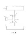
- FIG. 1is a schematic diagram of an exemplary SOI circuit device susceptible to charging damage
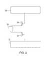
- FIG. 2is a schematic diagram of a circuit device with a charge-eliminating element, in accordance with an embodiment of the invention
- FIG. 3is a schematic diagram of a circuit device with an alternatively located charge-eliminating element
- FIG. 4is a flow diagram illustrating a method for reducing susceptibility to charging damage in SOI designs, in accordance with a further embodiment of the invention.
- SOIsilicon on insulator
- certain IC design structuressuch as SOI transistors, produce the possibility of charging damage.
- SOI transistorsFor example, it is possible to create a differential antenna by the arrangement of vias within the metal line. Vias placed in narrow metal lines have a larger aspect ratio than vias placed well within large metal plates, and may therefore charge to a different potential when exposed to a plasma. This occurs in either via-first or trough-first processes, although the specific sensitive process then varies. In generally, if the gate and source/drain of a FET have different via/metal configurations, then charging damage can occur.
- the chip designis segmented into multiple regions prior to tracing the electrical nets, and each FET is examined to ensure that any source/drain node of the FET is connected to only one transistor whose gate is connected to a large antenna.
- Multiple methods for eliminating the potential for charging damagemay be used.
- the connection to one of the large antennasmay be made at a higher wiring level to eliminate the potential for charging damage.
- the connection between the two FETsmay be made at a higher wiring level in the SOI circuit to eliminate the potential for charging damage.
- the circuit configurationis not complete, so at each level of wiring (M 1 , M 2 , etc.) the potential for charging damage is reassessed.
- the total number of nodes to be examinedreduces as higher levels of wiring are considered, until there is effectively only one single node at the final wiring level.
- the damagemay be observed to occur only on devices of a particular type, and in a particular configuration.
- “thick”(e.g., >2 nm) pFETs with high-aspect ratio vias on the gate nodemay be the only susceptible configuration, and all others may be safely ignored.
- the tracing processis performed assuming all metals and diffusions are conductive.
- different processesmay be implemented to determine whether a voltage differential exists across a series of two SOI transistors.
- One methodcompares the conductive shapes which are connected to the gate and source/drain to identify shapes with large charge accumulation properties (e.g., antenna). This can be accomplished using any conventional shapes processing program. For example, the method may obtain the length, width, height, etc., dimensions of the various conductors from the conventional shapes processing program and uses that data to perform the shapes comparison.
- a via embedded in a long thin metal wirewill have different antenna characteristics than a via within a wide plate. If the shapes are not balanced, the charge accumulation is likely to be unbalanced.
- FIG. 1illustrates a schematic diagram of an exemplary SOI circuit susceptible to charging damage.
- a first device 12is connected to a second device 13 , both of which are potentially susceptible to charging damage, as illustrated by a current 15 .
- Device 12may be, for example, a transistor, which has its gate connected to a large antenna 11 and its source/drain connected to the device 13 .
- device 13may be, for example, a transistor, which has its gate connected to a large antenna 10 and its source/drain connected to the device 12 .
- devices 12 and 13are identified as having the potential to be damaged because the charge accumulation on antenna 11 may be substantially different than the charge accumulation on antenna 10 .
- the physical separation of the two antennasmeans that each may possess a different potential, due to lateral nonuniformities.
- the devices 12 and 13may also be connected to a small antenna 14 .
- FIG. 2illustrates a schematic diagram of an exemplary circuit that has been designed to reduce eliminate the risk of charging damage, in accordance with an embodiment of the invention.
- a first device 22 and a second device 23are connected to each other through a higher level connection 26 .
- the higher level connection 26disrupts the potentially damaging current path that could lead to charging damage.
- Device 22may be, for example, a transistor, which has its gate connected to a large antenna 21 and its source/drain connected to the higher level connection 26 .
- device 23may be, for example, a transistor, which has its gate connected to a large antenna 10 and its source/drain connected to the higher level connection 26 .
- FIG. 3illustrates another schematic diagram of an exemplary circuit that has been designed to eliminate the risk of charging damage, in accordance with an alternative embodiment of the invention.
- a first device 32is connected to a second device 33 , which both may be connected to a small antenna 34 .
- Device 32may be, for example, a transistor, which has its gate connected to a large antenna 31 through the higher level connection 36 and its source/drain connected to the device 33 .
- the device 33may be, for example, a transistor, which has its gate connected to a large antenna 30 and its source/drain connected to the device 32 .
- FIG. 4illustrates a flow diagram of a method 50 for identifying susceptible devices and eliminating the risk of charging damage to the identified devices.
- the first step in the method 50is to assign one or more regions to the design under test (DUT), as shown at process block 52 .
- the next step in the method 50is to check for pairs of susceptible transistors in a diffusion node in the design, as shown at process block 54 . If a susceptible pair of transistors is found in a diffusion node the method may proceed to either process block 56 or 58 .
- the method 50breaks the connection between the two large antennas by inserting a higher level connection into the design (e.g., as shown in FIG. 3 ).
- the method 50breaks the connection between the transistor pair by making a higher level connection between the transistors (e.g., as shown in FIG. 2 ). If the method 50 does not find a susceptible pair of transistors in a diffusion node, the method returns to process block 54 and checks another diffusion node until all diffusion nodes have been checked. After all diffusion nodes have been checked, the method 50 terminates at process block 60 .
- the capabilities of the present inventioncan be implemented in software, firmware, hardware or some combination thereof.
- one or more aspects of the present inventioncan be included in an article of manufacture (e.g., one or more computer program products) having, for instance, computer usable media.
- the mediahas embodied therein, for instance, computer readable program code means for providing and facilitating the capabilities of the present invention.
- the article of manufacturecan be included as a part of a computer system or sold separately.
Landscapes
- Engineering & Computer Science (AREA)
- Computer Hardware Design (AREA)
- Physics & Mathematics (AREA)
- Theoretical Computer Science (AREA)
- Evolutionary Computation (AREA)
- Geometry (AREA)
- General Engineering & Computer Science (AREA)
- General Physics & Mathematics (AREA)
- Semiconductor Integrated Circuits (AREA)
- Metal-Oxide And Bipolar Metal-Oxide Semiconductor Integrated Circuits (AREA)
Abstract
Description
- 1. Field of the Invention
- The present invention generally relates to protection circuitry and, more particularly, to a method and structure that includes a local charge-eliminating element between the source/drain and gate of silicon-over-insulator (SOI) transistors which may develop a voltage differential between the source/drain and gate during wafer fabrication.
- 2. Description of Background
- One problem that exists when designing integrated circuits with silicon-over-insulator (SOI) transistors relates to the detection of which particular SOI transistors may be susceptible to charging damage, and to providing protection once such a susceptible device is identified. In SOI it is not possible to “tie down” a floating gate in the traditional sense, such as by adding a diode connection to the substrate or n-well. SOI technologies are inherently less susceptible to charging damage because both the source/drain and the gate tend to have similar antenna, so the potential of both nodes varies together. This is not, however, certain in all cases. The introduction of a charge-eliminating device or compensating antennas has been shown to reduce the propensity for damage; however, this approach is not always sufficient. If the connection between the source/drain and the gate nodes is too remote from the susceptible transistor, and the antennas connected to the source/drain and the gate of the transistor are too large, even a metallic shorting element may be not be of sufficiently low impedance to protect the transistor against damage.
- Disclosed is a protection circuit for an integrated circuit device, wherein said protection circuit includes: a first element connected to a gate of a first FET device; and a second element connected to a gate of a second FET device, wherein a drain/source of the first FET device and a drain/source of the second FET device are connected to a higher level connector and wherein the higher level connector eliminates a damaging current path between the first element and the second element.
- Also disclosed herein is a protection circuit for an integrated circuit device, wherein said protection circuit includes: a first element connected to a gate of a first FET device; a second element connected to a gate of a second FET device; wherein a drain/source of the first FET device and a drain/source of the second FET device are connected together, and the second element is connected through a higher level connector and wherein the higher level connector eliminates a damaging current path between the first element and the second element.
- Further disclosed herein is a method of preventing charging damage in an integrated circuit including: assigning a region to an integrated circuit design; identifying a pair of devices within the region as susceptible to charging damage; and modifying a structure of the region of the integrated circuit design, wherein the modification eliminates the potential for charging damage.
- These, and other, aspects and objects of the present invention will be better appreciated and understood when considered in conjunction with the following description and the accompanying drawings. It should be understood, however, that the following description, while indicating preferred embodiments of the present invention and numerous specific details thereof, is given by way of illustration and not of limitation. Many changes and modifications may be made within the scope of the present invention without departing from the spirit thereof, and the invention includes all such modifications.
- The invention will be better understood from the following detailed description with reference to the drawings, in which:
FIG. 1 is a schematic diagram of an exemplary SOI circuit device susceptible to charging damage;FIG. 2 is a schematic diagram of a circuit device with a charge-eliminating element, in accordance with an embodiment of the invention;FIG. 3 is a schematic diagram of a circuit device with an alternatively located charge-eliminating element; andFIG. 4 is a flow diagram illustrating a method for reducing susceptibility to charging damage in SOI designs, in accordance with a further embodiment of the invention.- The present invention and the various features and advantageous details thereof are explained more fully with reference to the non-limiting embodiments that are illustrated in the accompanying drawings and detailed in the following description. It should be noted that the features illustrated in the drawings are not necessarily drawn to scale. Descriptions of well-known components and processing techniques are omitted so as to not unnecessarily obscure the present invention in detail. The examples used herein are intended merely to facilitate an understanding of ways in which the invention may be practiced and to further enable those of skill in the art to practice the invention. Accordingly, the examples should not be construed as limiting the scope of the invention.
- To facilitate clarity, the invention will be described using a silicon on insulator (SOI) circuit example. In the foregoing example, certain IC design structures, such as SOI transistors, produce the possibility of charging damage. For example, it is possible to create a differential antenna by the arrangement of vias within the metal line. Vias placed in narrow metal lines have a larger aspect ratio than vias placed well within large metal plates, and may therefore charge to a different potential when exposed to a plasma. This occurs in either via-first or trough-first processes, although the specific sensitive process then varies. In generally, if the gate and source/drain of a FET have different via/metal configurations, then charging damage can occur. Elements connecting the source/drain node and the gate node together, either a metallic short, or a diode-connected FET, reduces the propensity of damage. However, in extreme cases this may not be sufficient if the protecting element is located too distant from the device to be protected.
- To address this problem, the chip design is segmented into multiple regions prior to tracing the electrical nets, and each FET is examined to ensure that any source/drain node of the FET is connected to only one transistor whose gate is connected to a large antenna. Multiple methods for eliminating the potential for charging damage may be used. In one example, the connection to one of the large antennas may be made at a higher wiring level to eliminate the potential for charging damage. In another example, the connection between the two FETs may be made at a higher wiring level in the SOI circuit to eliminate the potential for charging damage.
- During processing, the circuit configuration is not complete, so at each level of wiring (M1, M2, etc.) the potential for charging damage is reassessed. The total number of nodes to be examined reduces as higher levels of wiring are considered, until there is effectively only one single node at the final wiring level. Various degrees of refinement are possible, depending on the specifics of the particular technology. For example, the damage may be observed to occur only on devices of a particular type, and in a particular configuration. One such example is that “thick”(e.g., >2 nm) pFETs with high-aspect ratio vias on the gate node may be the only susceptible configuration, and all others may be safely ignored. In exemplary embodiments, the tracing process is performed assuming all metals and diffusions are conductive.
- In exemplary embodiments, different processes may be implemented to determine whether a voltage differential exists across a series of two SOI transistors. One method compares the conductive shapes which are connected to the gate and source/drain to identify shapes with large charge accumulation properties (e.g., antenna). This can be accomplished using any conventional shapes processing program. For example, the method may obtain the length, width, height, etc., dimensions of the various conductors from the conventional shapes processing program and uses that data to perform the shapes comparison. In one embodiment, a via embedded in a long thin metal wire will have different antenna characteristics than a via within a wide plate. If the shapes are not balanced, the charge accumulation is likely to be unbalanced.
FIG. 1 illustrates a schematic diagram of an exemplary SOI circuit susceptible to charging damage. Afirst device 12 is connected to asecond device 13, both of which are potentially susceptible to charging damage, as illustrated by a current15.Device 12 may be, for example, a transistor, which has its gate connected to alarge antenna 11 and its source/drain connected to thedevice 13. Likewise,device 13 may be, for example, a transistor, which has its gate connected to alarge antenna 10 and its source/drain connected to thedevice 12. As mentioned above,devices antenna 11 may be substantially different than the charge accumulation onantenna 10. The physical separation of the two antennas means that each may possess a different potential, due to lateral nonuniformities. In exemplary embodiments, thedevices small antenna 14.FIG. 2 illustrates a schematic diagram of an exemplary circuit that has been designed to reduce eliminate the risk of charging damage, in accordance with an embodiment of the invention. Afirst device 22 and asecond device 23 are connected to each other through ahigher level connection 26. Thehigher level connection 26 disrupts the potentially damaging current path that could lead to charging damage.Device 22 may be, for example, a transistor, which has its gate connected to alarge antenna 21 and its source/drain connected to thehigher level connection 26. Likewise,device 23 may be, for example, a transistor, which has its gate connected to alarge antenna 10 and its source/drain connected to thehigher level connection 26. By connecting thedevice higher level connection 26, the circuit design eliminates the damaging current path which made the circuit susceptible to charging damage.FIG. 3 illustrates another schematic diagram of an exemplary circuit that has been designed to eliminate the risk of charging damage, in accordance with an alternative embodiment of the invention. Afirst device 32 is connected to asecond device 33, which both may be connected to asmall antenna 34.Device 32 may be, for example, a transistor, which has its gate connected to alarge antenna 31 through thehigher level connection 36 and its source/drain connected to thedevice 33. Thedevice 33 may be, for example, a transistor, which has its gate connected to alarge antenna 30 and its source/drain connected to thedevice 32. By connecting thedevice 32 to thelarge antenna 31 through thehigher level connection 36, the circuit design eliminates the damaging current path between the twolarge antennas FIG. 4 illustrates a flow diagram of amethod 50 for identifying susceptible devices and eliminating the risk of charging damage to the identified devices. The first step in themethod 50 is to assign one or more regions to the design under test (DUT), as shown atprocess block 52. The next step in themethod 50 is to check for pairs of susceptible transistors in a diffusion node in the design, as shown atprocess block 54. If a susceptible pair of transistors is found in a diffusion node the method may proceed to eitherprocess block process block 56, themethod 50 breaks the connection between the two large antennas by inserting a higher level connection into the design (e.g., as shown inFIG. 3 ). Atprocess block 58, themethod 50 breaks the connection between the transistor pair by making a higher level connection between the transistors (e.g., as shown inFIG. 2 ). If themethod 50 does not find a susceptible pair of transistors in a diffusion node, the method returns to processblock 54 and checks another diffusion node until all diffusion nodes have been checked. After all diffusion nodes have been checked, themethod 50 terminates atprocess block 60.- The capabilities of the present invention can be implemented in software, firmware, hardware or some combination thereof.
- As one example, one or more aspects of the present invention can be included in an article of manufacture (e.g., one or more computer program products) having, for instance, computer usable media. The media has embodied therein, for instance, computer readable program code means for providing and facilitating the capabilities of the present invention. The article of manufacture can be included as a part of a computer system or sold separately.
- While the preferred embodiment to the invention has been described, it will be understood that those skilled in the art, both now and in the future, may make various improvements and enhancements which fall within the scope of the claims which follow. These claims should be construed to maintain the proper protection for the invention first described.
Claims (9)
1. A method of preventing charging damage in an integrated circuit comprising:
assigning a region to an integrated circuit design;
identifying a pair of devices within the region as susceptible to charging damage; and
modifying a structure of the region of the integrated circuit design, wherein the modification eliminates the potential for charging damage, wherein the pair of devices is a pair of transistors.
2. The method ofclaim 1 , wherein the pair of devices are series connected to a pair of antennas.
3. The method ofclaim 2 , wherein modifying a structure of the region of the integrated circuit design includes changing the electrical configuration of at least one of the antenna to eliminate potential charging damage.
4. The method ofclaim 2 , wherein modifying a structure of the region of the integrated circuit design includes changing the electrical connection placement of the two transistors to eliminate potential charging damage.
5. The method ofclaim 3 , wherein changing the electrical configuration of at least one of the antenna includes disconnecting one of the antenna from the pair of the devices.
6. The method ofclaim 4 , wherein changing the electrical connection placement of the two transistors includes moving the connection between the two transistors to a higher level.
7. The method ofclaim 2 , wherein modifying a structure of the region of the integrated circuit design includes changing the electrical connection placement of the two transistors to eliminate potential charging damage.
8. A protection circuit for an integrated circuit device, wherein said protection circuit comprises:
a first element connected to a gate of a first FET device; and
a second element connected to a gate of a second FET device the small antenna,
wherein a drain/source of the first FET device is connected to a drain/source of the second FET device and wherein the higher wiring level connector small antenna eliminates a damaging current path between the first element and the second element.
9. A protection circuit for an integrated circuit device, wherein said protection circuit comprises:
a first element connected to a gate of a first FET device; and
a second element connected to a gate of a second FET device,
wherein a drain/source of the first FET device and a drain/source of the second FET device are connected to a higher level connector, and
wherein the higher wiring level connector eliminates a damaging current path between the first element and the second element.
Priority Applications (1)
| Application Number | Priority Date | Filing Date | Title |
|---|---|---|---|
| US11/383,565US20070271540A1 (en) | 2006-05-16 | 2006-05-16 | Structure and method for reducing susceptibility to charging damage in soi designs |
Applications Claiming Priority (1)
| Application Number | Priority Date | Filing Date | Title |
|---|---|---|---|
| US11/383,565US20070271540A1 (en) | 2006-05-16 | 2006-05-16 | Structure and method for reducing susceptibility to charging damage in soi designs |
Publications (1)
| Publication Number | Publication Date |
|---|---|
| US20070271540A1true US20070271540A1 (en) | 2007-11-22 |
Family
ID=38713337
Family Applications (1)
| Application Number | Title | Priority Date | Filing Date |
|---|---|---|---|
| US11/383,565AbandonedUS20070271540A1 (en) | 2006-05-16 | 2006-05-16 | Structure and method for reducing susceptibility to charging damage in soi designs |
Country Status (1)
| Country | Link |
|---|---|
| US (1) | US20070271540A1 (en) |
Citations (13)
| Publication number | Priority date | Publication date | Assignee | Title |
|---|---|---|---|---|
| US5638006A (en)* | 1995-01-20 | 1997-06-10 | Vlsi Technology, Inc. | Method and apparatus for wafer level prediction of thin oxide reliability using differentially sized gate-like antennae |
| US5963412A (en)* | 1997-11-13 | 1999-10-05 | Advanced Micro Devices, Inc. | Process induced charging damage control device |
| US6005409A (en)* | 1996-06-04 | 1999-12-21 | Advanced Micro Devices, Inc. | Detection of process-induced damage on transistors in real time |
| US20020063298A1 (en)* | 2000-11-29 | 2002-05-30 | United Microelectronics Corp. | Semiconductor device for preventing process-induced charging damages |
| US6441397B2 (en)* | 2000-04-05 | 2002-08-27 | Matsushita Electronics Corporation | Evaluation of semiconductor chargeup damage and apparatus therefor |
| US6624480B2 (en)* | 2001-09-28 | 2003-09-23 | Intel Corporation | Arrangements to reduce charging damage in structures of integrated circuits |
| US6822840B2 (en)* | 2001-03-14 | 2004-11-23 | Taiwan Semiconductor Manufacturing Co., Ltd. | Method for protecting MOS components from antenna effect and the apparatus thereof |
| US20050098799A1 (en)* | 2003-11-04 | 2005-05-12 | Bonges Henry A.Iii | Method of assessing potential for charging damage in SOI designs and structures for eliminating potential for damage |
| US20060094164A1 (en)* | 2004-10-29 | 2006-05-04 | Nec Electronics Corporation | Semiconductor integrated device, design method thereof, designing apparatus thereof, program thereof, manufacturing method thereof, and manufacturing apparatus thereof |
| US20060115911A1 (en)* | 2004-11-12 | 2006-06-01 | Matsushita Electric Industrial Co., Ltd. | Layout verification method and method for designing semiconductor integrated circuit device using the same |
| US7160786B2 (en)* | 2001-10-29 | 2007-01-09 | Kawaski Microelectronics, Inc. | Silicon on insulator device and layout method of the same |
| US20070212799A1 (en)* | 2003-11-04 | 2007-09-13 | Hook Terence B | Method of Assessing Potential for Charging Damage in Integrated Circuit Designs and Structures for Preventing Charging Damage |
| US20070228479A1 (en)* | 2006-03-31 | 2007-10-04 | International Business Machines Corporation | Protection against charging damage in hybrid orientation transistors |
- 2006
- 2006-05-16USUS11/383,565patent/US20070271540A1/ennot_activeAbandoned
Patent Citations (17)
| Publication number | Priority date | Publication date | Assignee | Title |
|---|---|---|---|---|
| US5638006A (en)* | 1995-01-20 | 1997-06-10 | Vlsi Technology, Inc. | Method and apparatus for wafer level prediction of thin oxide reliability using differentially sized gate-like antennae |
| US6005409A (en)* | 1996-06-04 | 1999-12-21 | Advanced Micro Devices, Inc. | Detection of process-induced damage on transistors in real time |
| US5963412A (en)* | 1997-11-13 | 1999-10-05 | Advanced Micro Devices, Inc. | Process induced charging damage control device |
| US6441397B2 (en)* | 2000-04-05 | 2002-08-27 | Matsushita Electronics Corporation | Evaluation of semiconductor chargeup damage and apparatus therefor |
| US20020063298A1 (en)* | 2000-11-29 | 2002-05-30 | United Microelectronics Corp. | Semiconductor device for preventing process-induced charging damages |
| US6822840B2 (en)* | 2001-03-14 | 2004-11-23 | Taiwan Semiconductor Manufacturing Co., Ltd. | Method for protecting MOS components from antenna effect and the apparatus thereof |
| US6882014B2 (en)* | 2001-03-14 | 2005-04-19 | Taiwan Semiconductor Manufacturing Co., Ltd. | Protection circuit for MOS components |
| US6624480B2 (en)* | 2001-09-28 | 2003-09-23 | Intel Corporation | Arrangements to reduce charging damage in structures of integrated circuits |
| US7160786B2 (en)* | 2001-10-29 | 2007-01-09 | Kawaski Microelectronics, Inc. | Silicon on insulator device and layout method of the same |
| US20050098799A1 (en)* | 2003-11-04 | 2005-05-12 | Bonges Henry A.Iii | Method of assessing potential for charging damage in SOI designs and structures for eliminating potential for damage |
| US7067886B2 (en)* | 2003-11-04 | 2006-06-27 | International Business Machines Corporation | Method of assessing potential for charging damage in SOI designs and structures for eliminating potential for damage |
| US7132318B2 (en)* | 2003-11-04 | 2006-11-07 | International Business Machines Corporation | Method of assessing potential for charging damage in SOI designs and structures for eliminating potential for damage |
| US20070212799A1 (en)* | 2003-11-04 | 2007-09-13 | Hook Terence B | Method of Assessing Potential for Charging Damage in Integrated Circuit Designs and Structures for Preventing Charging Damage |
| US20060094164A1 (en)* | 2004-10-29 | 2006-05-04 | Nec Electronics Corporation | Semiconductor integrated device, design method thereof, designing apparatus thereof, program thereof, manufacturing method thereof, and manufacturing apparatus thereof |
| US20060115911A1 (en)* | 2004-11-12 | 2006-06-01 | Matsushita Electric Industrial Co., Ltd. | Layout verification method and method for designing semiconductor integrated circuit device using the same |
| US20070228479A1 (en)* | 2006-03-31 | 2007-10-04 | International Business Machines Corporation | Protection against charging damage in hybrid orientation transistors |
| US20080108186A1 (en)* | 2006-03-31 | 2008-05-08 | Hook Terence B | Method of providing protection against charging damage in hybrid orientation transistors |
Similar Documents
| Publication | Publication Date | Title |
|---|---|---|
| US7132318B2 (en) | Method of assessing potential for charging damage in SOI designs and structures for eliminating potential for damage | |
| US8564364B2 (en) | Countermeasure method and device for protecting against a fault injection attack by detection of a well voltage crossing a threshold | |
| US6493850B2 (en) | Integrated circuit design error detector for electrostatic discharge and latch-up applications | |
| US7560345B2 (en) | Method of assessing potential for charging damage in integrated circuit designs and structures for preventing charging damage | |
| US20140362482A1 (en) | Electrostatic discharge structure for enhancing robustness of charge device model and chip with the same | |
| US8054597B2 (en) | Electrostatic discharge structures and methods of manufacture | |
| US6624480B2 (en) | Arrangements to reduce charging damage in structures of integrated circuits | |
| US9741707B2 (en) | Immunity to inline charging damage in circuit designs | |
| US20200235571A1 (en) | Protection Circuit for Signal Processor | |
| US6566716B2 (en) | Arrangements to reduce charging damage in structures of integrated circuits using polysilicon or metal plate(s) | |
| US20080310059A1 (en) | Esd protection design method and related circuit thereof | |
| US9312691B2 (en) | ESD protection circuit and ESD protection method thereof | |
| US20070271540A1 (en) | Structure and method for reducing susceptibility to charging damage in soi designs | |
| EP3147945A1 (en) | Esd detection circuit | |
| Yousaf et al. | Rapid characterization of efficient system level ESD protection strategy using coupling transfer function | |
| KR100523504B1 (en) | Semiconductor integrated circuit device, mounting substrate apparatus and wire cutting method thereof | |
| US6414358B1 (en) | Arrangements to reduce charging damage in structures of integrated circuits | |
| US10147175B2 (en) | Detection of hardware trojan using light emissions with sacrificial mask | |
| CN116629197A (en) | Layout detection method | |
| TWI666755B (en) | Electrostatic discharge protection structure, integrated circuit, and method for protecting core circuit of integrated circuit from electrostatic discharge event received by conductive pad of the integrated circuit | |
| US7889468B2 (en) | Protection of integrated electronic circuits from electrostatic discharge | |
| US20230198250A1 (en) | Electrostatic discharge protection circuit | |
| US12218120B2 (en) | Device mismatch mitigation for medium range and beyond distances | |
| US20090094567A1 (en) | Immunity to charging damage in silicon-on-insulator devices | |
| Kang et al. | 87‐1: A Study on the Optimal Design of ESD Protection Circuit in OLED Panel Using Electromagnetic Simulation |
Legal Events
| Date | Code | Title | Description |
|---|---|---|---|
| AS | Assignment | Owner name:INTERNATIONAL BUSINESS MACHINES CORPORATION, NEW Y Free format text:ASSIGNMENT OF ASSIGNORS INTEREST;ASSIGNORS:ENG, CHUNG-PING;BONGES, III, HENRY A.;ZIMMERMAN, JEFFREY S.;AND OTHERS;REEL/FRAME:017628/0792;SIGNING DATES FROM 20060511 TO 20060517 | |
| STCB | Information on status: application discontinuation | Free format text:ABANDONED -- FAILURE TO RESPOND TO AN OFFICE ACTION | |
| AS | Assignment | Owner name:GLOBALFOUNDRIES U.S. 2 LLC, NEW YORK Free format text:ASSIGNMENT OF ASSIGNORS INTEREST;ASSIGNOR:INTERNATIONAL BUSINESS MACHINES CORPORATION;REEL/FRAME:036550/0001 Effective date:20150629 | |
| AS | Assignment | Owner name:GLOBALFOUNDRIES INC., CAYMAN ISLANDS Free format text:ASSIGNMENT OF ASSIGNORS INTEREST;ASSIGNORS:GLOBALFOUNDRIES U.S. 2 LLC;GLOBALFOUNDRIES U.S. INC.;REEL/FRAME:036779/0001 Effective date:20150910 |