US20070268761A1 - Integrated circuit having memory array including row redundancy, and method of programming, controlling and/or operating same - Google Patents
Integrated circuit having memory array including row redundancy, and method of programming, controlling and/or operating sameDownload PDFInfo
- Publication number
- US20070268761A1 US20070268761A1US11/804,098US80409807AUS2007268761A1US 20070268761 A1US20070268761 A1US 20070268761A1US 80409807 AUS80409807 AUS 80409807AUS 2007268761 A1US2007268761 A1US 2007268761A1
- Authority
- US
- United States
- Prior art keywords
- row address
- decoded
- memory
- redundant row
- redundancy
- Prior art date
- Legal status (The legal status is an assumption and is not a legal conclusion. Google has not performed a legal analysis and makes no representation as to the accuracy of the status listed.)
- Granted
Links
Images


Classifications
- G—PHYSICS
- G11—INFORMATION STORAGE
- G11C—STATIC STORES
- G11C8/00—Arrangements for selecting an address in a digital store
- G11C8/20—Address safety or protection circuits, i.e. arrangements for preventing unauthorized or accidental access
- G—PHYSICS
- G11—INFORMATION STORAGE
- G11C—STATIC STORES
- G11C11/00—Digital stores characterised by the use of particular electric or magnetic storage elements; Storage elements therefor
- G11C11/21—Digital stores characterised by the use of particular electric or magnetic storage elements; Storage elements therefor using electric elements
- G11C11/34—Digital stores characterised by the use of particular electric or magnetic storage elements; Storage elements therefor using electric elements using semiconductor devices
- G11C11/40—Digital stores characterised by the use of particular electric or magnetic storage elements; Storage elements therefor using electric elements using semiconductor devices using transistors
- G11C11/41—Digital stores characterised by the use of particular electric or magnetic storage elements; Storage elements therefor using electric elements using semiconductor devices using transistors forming static cells with positive feedback, i.e. cells not needing refreshing or charge regeneration, e.g. bistable multivibrator or Schmitt trigger
- G11C11/413—Auxiliary circuits, e.g. for addressing, decoding, driving, writing, sensing, timing or power reduction
- G—PHYSICS
- G11—INFORMATION STORAGE
- G11C—STATIC STORES
- G11C29/00—Checking stores for correct operation ; Subsequent repair; Testing stores during standby or offline operation
- G11C29/70—Masking faults in memories by using spares or by reconfiguring
- G11C29/78—Masking faults in memories by using spares or by reconfiguring using programmable devices
- G11C29/80—Masking faults in memories by using spares or by reconfiguring using programmable devices with improved layout
- G11C29/802—Masking faults in memories by using spares or by reconfiguring using programmable devices with improved layout by encoding redundancy signals
- G—PHYSICS
- G11—INFORMATION STORAGE
- G11C—STATIC STORES
- G11C29/00—Checking stores for correct operation ; Subsequent repair; Testing stores during standby or offline operation
- G11C29/70—Masking faults in memories by using spares or by reconfiguring
- G11C29/78—Masking faults in memories by using spares or by reconfiguring using programmable devices
Definitions
- the inventions described and illustrated hereinrelate to an integrated circuit device having a memory cell array including row redundancy, and techniques for programming, configuring, controlling and/or operating such device; and more particularly, in one aspect, to an integrated circuit having random access memory (“RAM”) array having a plurality of memory cells (for example, memory cells having an electrically floating body in which an electrical charge is stored) arranged in a matrix of rows and columns wherein the integrated circuit includes a row redundancy architecture including at least one redundant row to substitute or replace a row of memory cells having at least one defective memory cell.
- RAMrandom access memory
- memory cell array 10typically includes a plurality of memory cells 12 arranged in a matrix of rows 14 (each typically having a common word line 16 ) and columns 18 .
- a row address decoder 20enables one or more rows to be read by sensing circuitry 22 (for example, a plurality of sense amplifiers).
- sensing circuitry 22for example, a plurality of sense amplifiers.
- redundant rows 14 rare often incorporated into memory array 10 to logically “replace” one or more rows 14 having one or more defective memory cells 12 .
- row redundancyis implemented by including a redundant address decoder 20 r which is programmed or mapped to logically replace a defective row (i.e., a row of memory cells having one or more defective memory cells) with spare, replacement, redundant or another row 14 r of memory cells 12 r in memory array 10 (i.e., redundant row 14 r of memory cells 12 r ).
- the individual address comparators (not illustrated) of redundant row decoder 20 rare programmed to “enable” spare or redundant word line drivers 24 r when the “applied” address matches the address of the defective row (which is fixed/stored in redundant row address decoder 20 r ).
- the addresses of the defective word lines 16are programmed into address comparators of redundant row decoder 20 r during wafer testing.
- the redundant row address comparatorsenable a spare or redundant word line (which define the redundant row 14 r memory cells 12 ) to be active when a set of row address signals match the address of a defective row 14 (or word line 16 ) which is programmed into redundant row address decoder 20 r.
- redundant row decoder 20 ris programmed via configuring the state of a set of fuses 26 .
- spare or redundant rowsare programmed by selectively “blowing” fuses 26 within redundant row decoder 20 r to “match” or correspond to the address of the rows having defective memory cells.
- Such fusesare often programmed prior to packaging, during the wafer testing stage, or immediately after packaging, during the device testing stage. In this way, spare or redundant word line drivers 24 r are enabled when the address matches the address programmed into redundant row decoder 20 r.
- circuitry 28is implemented in memory array 10 to disable row 14 having the defective memory cells when the address matches the address programmed into redundant row decoder 20 r, and spare or redundant word line drivers 24 r are enabled.
- circuitry 28in response to a “match” between the applied or incoming row address and the address programmed in redundant row decoder 20 r, normal word line drivers 24 are disabled and redundant word line drivers 24 r are enabled.
- the present inventionsare directed to an integrated circuit device (for example, logic device or discrete memory device) comprising a memory cell array having a plurality of memory cells arranged in a matrix of rows and columns including (i) a plurality of normal rows of memory cells which are associated with and selectable via normal row addresses and (ii) a redundant row of memory cells which is associated with and selectable via a redundant row address.
- an integrated circuit devicefor example, logic device or discrete memory device
- a memory cell arrayhaving a plurality of memory cells arranged in a matrix of rows and columns including (i) a plurality of normal rows of memory cells which are associated with and selectable via normal row addresses and (ii) a redundant row of memory cells which is associated with and selectable via a redundant row address.
- the integrated circuit devicefurther includes address decoder circuitry to generate decoded row address data in response to an applied row address, normal word line drivers, coupled to the address decoder circuitry and the plurality of normal rows of memory cells, to responsively enable one or more normal rows of memory cells using the decoded row address data, and redundant word line drivers, coupled to the address decoder circuitry and the redundant row of memory cells, to responsively enable the redundant row of memory cells using the decoded row address data.
- the integrated circuit device of this aspectincludes redundancy address evaluation circuitry, coupled to the address decoder circuitry, the normal word line drivers and the redundant word line drivers, to (i) store decoded redundant row address data which corresponds to the redundant row address, and (ii) in operation, determine whether the decoded row address data corresponds to the decoded redundant row address data, and, in response thereto, to enable the redundant word line drivers.
- the redundancy address evaluation circuitrymay include a memory to temporarily store the decoded redundant row address data.
- the redundancy address evaluation circuitrymay also include a comparator logic circuitry to compare the decoded row address data and the decoded redundant row address data which is temporarily stored in the memory and, in response to a match, to enable the redundant word line drivers and disable the normal word line drivers.
- the memoryin response to a control signal, stores the decoded redundant row address data provided by the address decoder circuitry.
- the memoryin response to a control signal, stores the decoded redundant row address data generated by the address decoder circuitry.
- the memorymay permanently store the decoded redundant row address data.
- the redundancy address evaluation circuitrymay include a comparator logic circuitry to compare the decoded row address data and the decoded redundant row address data which is stored in the memory and, in response to a match, to enable the redundant word line drivers and disable the normal word line drivers.
- the memoryin response to a control signal, stores the decoded redundant row address data provided by the address decoder circuitry.
- the memoryin response to a control signal, stores the decoded redundant row address data generated by the address decoder circuitry.
- the integrated circuit devicemay also include controller circuitry, coupled to the address decoder circuitry and the redundancy address evaluation circuitry, to generate and/or determine (i) the redundant row address and (ii) the control signal, wherein in response thereto, the address decoder circuitry generates decoded redundant row address data and the redundancy address evaluation circuitry stores the decoded redundant row address data.
- controller circuitrycoupled to the address decoder circuitry and the redundancy address evaluation circuitry, to generate and/or determine (i) the redundant row address and (ii) the control signal, wherein in response thereto, the address decoder circuitry generates decoded redundant row address data and the redundancy address evaluation circuitry stores the decoded redundant row address data.
- the controller circuitrymay determine the redundant row address based on detecting one or more bit failures or anticipated bit failures of memory cells of a row of memory cells of the plurality of normal rows of memory cells. In one embodiment, the controller circuitry generates (i) the redundant row address and (ii) the control signal, wherein in response thereto, the address decoder circuitry generates decoded redundant row address data and the redundancy address evaluation circuitry stores the decoded redundant row address data.
- the present inventionsare directed to a method of programming a redundant row of memory cells into an integrated circuit device
- the integrated circuit deviceincludes (a) a memory cell array having a plurality of memory cells arranged in a matrix of rows and columns including (i) a plurality of normal rows of memory cells which are associated with and selectable via normal row addresses and (ii) a redundant row of memory cells which is associated with and selectable via a redundant row address, (b) address decoder circuitry to generate decoded row address data in response to an applied row address, and (c) a redundancy memory.
- the methodincludes determining the redundant row address based on detecting one or more bit failures or anticipated bit failures of memory cells of a row of memory cells of the plurality of normal rows of memory cells, generating a decoded redundant row address data which corresponds to the redundant row address via the address decoder, generating a redundancy program signal, and storing the decoded redundant row address data in the redundancy memory in response to a redundancy program signal.
- the methodmay further include temporarily or permanently storing the decoded redundant row address data in the redundancy memory in response to a redundancy program signal.
- the present inventionsare directed to a method of operating an integrated circuit device including (a) a memory cell array having a plurality of memory cells arranged in a matrix of rows and columns including (i) a plurality of normal rows of memory cells which are associated with and selectable via normal row addresses and (ii) a redundant row of memory cells which is associated with and selectable via a redundant row address, (b) address decoder circuitry to generate decoded row address data in response to an applied row address, (c) a redundancy memory to store decoded redundant row address data, (d) normal word line drivers and (e) redundant word line drivers.
- the methodcomprises generating decoded row address data in response to an applied row address, responsively enabling (i) at least one of the normal rows of memory cells or (ii) the redundant row of memory cells using the decoded row address data, and determining, during operation, whether the decoded row address data corresponds to the decoded redundant row address data stored in the redundancy memory, and, in response thereto, enabling the redundant word line drivers and disabling the normal word line drivers.
- the method of this aspect of the inventionsmay include generating decoded redundant row address data which corresponds to the redundant row address via the address decoder, and storing the decoded redundant row address data in the redundancy memory in response to a redundancy program signal.
- the methodmay also include determining the redundant row address based on detecting one or more bit failures or anticipated bit failures of memory cells of a row of memory cells of the plurality of normal rows of memory cells, generating a decoded redundant row address data which corresponds to the redundant row address via the address decoder, generating a redundancy program signal, and storing the decoded redundant row address data in the redundancy memory in response to a redundancy program signal.
- the methodmay further include generating a decoded redundant row address data which corresponds to the redundant row address via the address decoder, generating a redundancy program signal and storing the decoded redundant row address data in the redundancy memory in response to a redundancy program signal.
- the methodmay include generating a decoded redundant row address data which corresponds to the redundant row address via the address decoder, and storing the decoded redundant row address data in the redundancy memory.
- the methodmay include temporarily storing the decoded redundant row address data in the redundancy memory in response to a redundancy program signal.
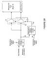
- FIG. 1Ais an exemplary schematic block diagram illustration of a conventional memory cell array having a plurality of memory cells arranged in an array of a plurality of rows and columns, in conjunction with row address decoders, word line drivers and data sense circuitry;
- FIG. 1Bis an exemplary schematic block diagram illustration of the conventional row redundancy architecture
- FIG. 1Cis an exemplary schematic block diagram illustration of the conventional circuitry to program the redundant row decoder circuitry which, in this example, includes a plurality of fuses;
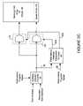
- FIGS. 2A-2Dare schematic block diagram illustrations of exemplary embodiments of the row redundancy architecture, in conjunction with memory cell array (having redundant rows), according to certain aspects of the present inventions;
- FIGS. 3A and 3Bare schematic block diagram illustrations of exemplary embodiments of the row address decoder circuitry, according to certain aspects of the present inventions.
- FIGS. 4A and 4Bare schematic block diagram illustrations of exemplary embodiments of the redundancy address evaluation circuitry, according to certain aspects of the present inventions.
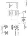
- FIGS. 5 and 6are schematic block diagram illustrations of exemplary embodiments of the row redundancy architecture, in conjunction with memory cell array (having redundant rows) and controller circuitry, according to certain aspects of the present inventions.
- FIGS. 7A-7Care schematic block diagram illustrations of an exemplary devices in which the row redundancy architecture may be implemented wherein FIG. 7A and 7C are logic devices (having logic circuitry and resident memory) and FIG. 7B is a memory device (having primarily of a memory array), according to certain aspects of the present inventions.
- the present inventionsare directed to row redundancy architectures and techniques, including row redundancy circuitry for a memory cell array having a plurality of memory cells, arranged in a matrix of rows and columns.
- the present inventionsare directed to methods of programming, configuring, controlling and/or operating such row redundancy circuitry.
- the memory cell array and redundancy circuitrymay comprise a portion of an integrated circuit device, for example, a logic device (such as, a microcontroller or microprocessor) or a portion of a memory device (such as, a discrete memory).
- redundancy architectures implemented according to the present inventionsmay make more efficient use of the pre-existing addressing circuitry (for example, the row pre-decoders and decoders). Moreover, the present inventions may provide a significant area and power savings because, among other things, the redundant row address decoder (as described above with reference to FIGS. 1A-1C ) may be eliminated. Such redundancy circuitry is quite large, often consuming as much area as the normal row decoders.
- the present inventionsmay be implemented in conjunction with any memory cell technology, whether now known or later developed.
- the memory cellsmay include one or more transistors having electrically floating body regions, one transistor-one capacitor architectures, electrically floating gate transistors, junction field effect transistors (often referred to as JFETs), or any other memory/transistor technology whether now known or later developed. All such memory technologies are intended to fall within the scope of the present inventions.
- the present inventionsmay be implemented in conjunction with any type of memory (including discrete or integrated with logic devices), whether now known or later developed.
- the memorymay be a DRAM, SRAM and/or Flash. All such memories are intended to fall within the scope of the present inventions.
- the memory cells of the memory cell arraymay include at least one transistor having an electrically floating body transistor which stores an electrical charge in the electrically floating body region thereof.
- the amount of charge stored in the in the electrically floating body regioncorrelates to the data state of the memory cell.
- One type of such memory cellis based on, among other things, a floating body effect of semiconductor on insulator (SOI) transistors.
- SOIsemiconductor on insulator
- Patent Application Publication No. 2007/0058427(“Memory Cell and Memory Cell Array Having an Electrically Floating Body Transistor, and Methods of Operating Same”), (4) U.S. Non-Provisional patent application Ser. No. 11/633,311, Okhonin, filed Dec. 4, 2006 and entitled “Electrically Floating Body Memory Cell and Array, and Method of Operating or Controlling Same”, and (5) U.S. Non-Provisional patent application Ser. No. 11/703,429, Okhonin et al., filed on Feb. 7, 2007 and entitled “Multi-Bit Memory Cell Having Electrically Floating Body Transistor, and Method of Programming and Reading Same”, all of which are incorporated by reference herein in its entirety).
- the memory cellmay consist of a partially depleted (PD) or a fully depleted (FD) SOI transistor or bulk transistor (transistor which formed in or on a bulk material/substrate) having a gate, which is disposed adjacent to the electrically floating body and separated therefrom by a gate dielectric.
- the body region of the transistoris electrically floating in view of the insulation or non-conductive region, for example, in bulk-type material/substrate, disposed beneath the body region.
- the state of memory cellmay be determined by the concentration or amount of charge contained or stored in the body region of the SOI or bulk transistor.
- the row redundancy architectureincludes redundancy address evaluation circuitry 50 electrically coupled to address decoder circuitry 52 to receive a set of input signals which are representative of the applied row address that is decoded by address decoder circuitry 52 .
- redundancy address evaluation circuitry 50includes comparator logic circuitry 56 and memory 58 . (See, for example, FIG. 4A ). The output(s) of redundancy address evaluation circuitry 50 is applied to word line drivers 24 and redundant word line drivers 24 r to responsively enable/disable drivers 24 and 24 r.
- the comparator logic circuitry 56includes circuitry that compares the decoded address with a decoded address which is stored in memory 58 .
- the comparator logic circuitry 56may be any type of circuitry, whether now known or later developed, that compares data (for example, discrete circuitry or logic, state machine, processor or the like, whether digital or analog circuitry, and/or whether hardwired or programmable); all such circuitry is intended to fall within the scope of the present inventions.
- comparator logic circuitry 56may be a plurality of EX-OR logic gates (see, for example, FIG.
- a plurality of AND logic gates or other logic circuitrywhich are interconnected to determine whether the decoded address data (here, the output of address decoder circuitry 52 which is representative of the decoded row address that is applied to address decoder circuitry 52 via decoded address signal lines 54 ) “matches” data which is representative of the decoded row address having one or more defective memory cells (i.e., a defective row of memory cells).
- the memory 58stores data which is representative of a decoded row address that corresponds to an address of a row of memory cells (for example, including one or more defective or inoperative memory cells) that is to be “replaced” by the redundant or spare row of memory cells.
- the memory 58may be any circuitry, whether now known or later developed, that stores data (here, the decoded row address which represents the row having the defective memory cells).
- memory 58may be one or more fuses or anti-fuses, or DRAM, SRAM, PROM, EPROM, EEPROM cells, and/or latch or register circuitry (for example, a plurality of latches or registers).
- latch or register circuitryfor example, a plurality of latches or registers.
- the decoded row address datamay be stored in memory 58 (for example, a latch or register) in response to a store control signal (or redundancy program signal) applied on redundancy program signal line 60 .
- row decoder 20decodes the row address of the row of memory cells to be substituted or replaced by the redundant or spare row of memory cells 14 r.
- the row addressin a decoded form, is provided to memory 58 via signal lines 54 .
- memory 58stores the decoded row address data in memory 58 .
- well known programming techniquesmay be employed to store the decoded row address data in the fuses or anti-fuses.
- row address decoder circuitry 52receives a row address and, in response, generates a decoded row address which corresponds to the applied row address.
- the decoded row addressis provided to, among other things, redundancy address evaluation circuitry 50 which determines whether the decoded row address data corresponds to or “matches” data stored in memory 58 .
- comparator logic circuitry 56determines a “match” between the decoded row address data and the data stored in memory 58 , comparator logic circuitry 56 generates a redundancy/spare row enable signal on signal line 62 .
- the redundancy/spare row enable signalenables redundant word line drivers 24 r and disables normal word line drivers 24 . In this way, memory cells 12 associated with redundant word line 16 r are accessed (for example, read from or written to) while the memory cells 12 associated with “replaced” word line 16 (and driven by an associated word line driver 24 ) are not accessed.
- word line drivers 24are employed to access an associated row 14 of memory cells and word line drivers 24 r are disabled. Under this circumstance, the applied row address does not correspond to a row of memory cells to be “replaced” or “substituted” by the redundant or spare row(s) of memory cells.
- memory 58stores data which is representative of one or more decoded row addresses that correspond to one or more row addresses of memory cells (for example, including one or more defective or inoperative memory cells) that is/are to be “replaced” or “substituted” by the redundant or spare row(s) of memory cells.
- the memory 58may be one time programmable (for example, programmed during test or at manufacture) or more than one time programmable (for example, during test, start-up/power-up, during an initialization sequence and/or during operation (in situ)).
- the data which is representative of the decoded row addressmay be “stored” in memory 58 , for example, at start-up/power-up and/or during an initialization sequence.
- the address(es) of the row(s) of memory cells to be “replaced” or “substituted” by the redundant or spare row(s) of memory cellsmay be provided and/or determined by external (i.e., off-chip—for example, resident on a common printed circuit board) or internal/integrated circuitry (i.e., on-chip).
- the decoded row address data(which correspond to one or more row addresses of memory cells including, for example, one or more defective or inoperative memory cells) may be provided by a controller at, for example, start-up/power-up, during an initialization sequence and/or during operation.
- controller circuitry 64for example, built-in self-test (BIST) circuitry
- BISTbuilt-in self-test
- controller circuitry 64In response to detecting one or more memory cells to be “replaced”, controller circuitry 64 applies the associated row address or addresses of such memory cells to row decoder circuitry 52 and, in addition, applies the store data signal (redundancy program signal) 60 to redundancy address evaluation circuitry 50 (and, in particular, to memory 58 ).
- the decoded row address datais provided to redundancy address evaluation circuitry 50 (via signal lines 54 ) and, in response to the store data signal (or redundancy program signal) 60 , data which is representative of the decoded row address (for example, a defective row) is stored in memory 58 (for example, stored in a latch).
- the programming of the redundancy circuitrymay be a one-time process, for example, during start-up/power-up and/or during an initialization sequence.
- the programmingmay also be in situ, for example, in response to detection of a bit failure or anticipated bit failure by controller circuitry 64 , for example, during operation of the memory cell array 10 .
- the controller circuitry 64may be any type of circuitry (for example, discrete circuitry or logic, state machine, processor or the like, whether digital or analog circuitry, and/or whether hardwired or programmable) that may detect one or more defective or inoperative memory cells.
- controller circuitry 64may be external (non-integrated) circuitry or internal (integrated) circuitry, such as, for example, BIST circuitry.
- BIST circuitrySee, for example, “A 30-ns 64-MB DRAM with Built-in Self-Test and Self-Repair Function”, Tanabe et al., IEEE Journal of Sold-Sate Circuits, Vol. 27, No. 11, November 1992, pp. 1525-1533).
- all forms or types of circuitry that are suitable to detect one or more defective or inoperative memory cells, whether now known or later developed,is intended to fall within the scope of the present inventions.
- address decoder circuitry 52receives “normal” row addresses and separate redundant row address(es).
- the “normal” row addressesare addresses that are applied during normal operation and the redundant row address(es) correspond to row(s) of memory cells that are to be “replaced” or “substituted” by redundant or spare row(s) 14 r.
- the “normal” row addressesmay be addresses which correspond to operative or inoperative/defective rows in memory cell array 10 .
- the redundant row address(es)are addresses that are applied to address decoder circuitry 52 during the programming or configuration of the redundancy circuitry (for example, programming of redundancy address evaluation circuitry 50 ).
- multiplexer circuitry 66provides the row addresses to row address decoder 20 .
- a store data signal(or redundancy program signal 60 ) is applied to multiplexer circuitry 66 (see FIG. 3B ) which instructs/causes multiplexer circuitry 66 to provide the address applied to the redundant row address inputs to row address decoder 20 .
- row address decoder 20decodes the address associated with a row(s) of memory cells that is/are to be “replaced” or “substituted” by the redundant or spare row(s) 14 r.
- the decoded row address data(which is representative of row 14 that is being “replaced” or “substituted” by the redundant or spare row(s) 14 r) is provided to redundancy address evaluation circuitry 50 .
- the memory 58in response to the redundancy program signal applied on signal line 60 , stores the decoded row address data.
- the embodiment of FIGS. 2B , 3 B and 4 Amay operate in the same manner as discussed above with respect to the embodiment of FIGS. 2A , 3 A and 4 A.
- the entire discussion above, relative to the embodiment of FIGS. 2A , 3 A and 4 A,is entirely applicable to the embodiment of FIGS. 2B , 3 B and 4 A. For the sake of brevity, those discussions will not be repeated in detail but are discussed briefly below.
- row address decoder circuitry 52receives a row address applied on the “normal” row address lines and, row decoder 20 responsively decodes the address.
- the decoded row addressis provided to, among other things, redundancy address evaluation circuitry 50 which determines whether the decoded row address data corresponds to or “matches” data stored in memory 58 .
- the comparator logic circuitry 56compares the decoded row address data to the data stored in memory 58 . Where the decoded row address data does not correspond to the data stored in memory 58 , word line drivers 24 are employed to access an associated row 14 of memory cells and redundant word line drivers 24 r are disabled.
- comparator logic circuitry 56determines a “match” between the decoded row address data and the data stored in memory 58 , comparator logic circuitry 56 generates a redundancy/spare row enable signal on signal line 62 .
- the redundancy/spare row enable signaldisables normal word line drivers 24 corresponding to the row address and enables redundant word line drivers 24 r. In this way, memory cells 12 associated with redundant word line 16 r are accessed (for example, read from or written to) while the memory cells 12 associated with “replaced” word line 16 (and driven by an associated word line driver 24 ) are not accessed.
- controller circuitry 64generates the redundant row address(es).
- controller circuitry 64(i) generates corresponding row addresses to be provided to addresses decoder circuitry 52 , and (ii) generates the store data signal or redundancy program signal on signal line 60 to enable memory 58 to store data which is representative of the decoded row address data (which correspond to one or more row addresses of memory cells, for example, including one or more defective or inoperative memory cells).
- controller circuitry 64(for example, BIST circuitry) may program the redundancy circuitry at, for example, start-up/power-up, during an initialization sequence and/or during operation.
- controller circuitry 64(i) detects one or more rows of memory cells to be “replaced” or “substituted” by one or more redundant or spare rows, (ii) generates corresponding row addresses to be provided to addresses decoder circuitry 52 , and (iii) generates the store data signal or redundancy program signal on signal line 60 to enable memory 58 to store data which is representative of the decoded row address data.
- controller circuitry 64(for example, BIST circuitry) may detect one or more defective or inoperative memory cells of memory cell array 10 .
- controller circuitry 64In response to detecting, for example, one or more defective memory cells, controller circuitry 64 applies the row address(es) associated with such memory cells to row decoder circuitry 52 (via signal lines 68 ). In addition, controller circuitry 64 may enable memory 58 (via signal line 60 ) to store the decoded address data. As mentioned above, the decoded row address data is provided to redundancy address evaluation circuitry 50 (via signal lines 54 ) and, in response to the store data signal (or redundancy program signal), the data which is representative of the decoded row address is stored in memory 58 (for example, stored in a latch or register).
- programming the redundancy circuitrymay be a one-time process, for example, during start-up/power-up and/or during an initialization sequence.
- the programmingmay also be in situ, for example, in response to detection of a bit failure or anticipated bit failure by controller circuitry 64 , for example, during operation of the memory cell array 10 .
- the present inventionsmay be implemented in a logic device having a memory portion and logic portion (see, for example, FIGS. 7A and 7C ), or an integrated circuit that is primarily a memory device (see, for example, FIG. 7B ).
- the logic devicemay be, for example, a processor, controller, field programmable gate array, state machine, and/or a device including same.
- the present inventionsmay be implemented in any device employing a memory array and redundancy architecture or technique.
- the present inventionsmay be employed in conjunction with any memory cell technology now known or later developed.
- the present inventionsmay be implemented in conjunction with a memory array, having a plurality of memory cells each including an electrically floating body transistor.
- a memory arrayhaving a plurality of memory cells each including an electrically floating body transistor.
- 2007/0058427(“Memory Cell and Memory Cell Array Having an Electrically Floating Body Transistor, and Methods of Operating Same”)
- the memory cellmay consist of a PD or a FD SOI transistor (or transistor formed on or in bulk material/substrate) having a gate, which is disposed adjacent to the electrically floating body and separated therefrom by a gate dielectric.
- the body region of the transistoris electrically floating in view of the insulation or non-conductive region (for example, in bulk-type material/substrate) disposed beneath the body region.
- the state of memory cellis determined by the concentration of charge within the body region of the SOI transistor.
- the memory cells of the memory cell arraymay be comprised of N-channel, P-channel and/or both types of transistors.
- circuitry that is peripheral to the memory arrayfor example, sense amplifiers or comparators, row and column address decoders, as well as line drivers (not illustrated in detail herein)
- N-channel type transistors or P-channel type transistorsare employed as memory cells 12 in the memory array(s) 10
- suitable write and read voltagesare well known to those skilled in the art (and in view of the U.S. Patents and U.S. patent applications incorporated herein by reference).
- integrated circuit devicefor example, memory or logic device
- integrated circuit devicemay include a plurality of memory cell arrays, each having a plurality of memory cells, wherein certain of the circuitry (for example, redundancy address evaluation circuitry 50 ) is dedicated to one or more arrays and controller circuitry 64 is shared among the arrays.
- the present inventionsmay be employed or implemented in conjunction with one or more of the inventions, memory cells, memory arrays, and techniques for programming, reading, controlling and/or operating a memory cell and array including, for example, (1) Okhonin et al., U.S. Patent Application Publication No. 2006/0131650 (“Bipolar Reading Technique for a Memory Cell Having an Electrically Floating Body Transistor”), (2) Okhonin et al., U.S. Patent Application Publication No. 2007/0058427 (“Memory Cell and Memory Cell Array Having an Electrically Floating Body Transistor, and Methods of Operating Same”), (3) U.S. Non-Provisional patent application Ser. No.
- the memory cellsmay be arranged, configured and/or controlled using any of the memory cell arrays, architectures and/or control/operation techniques.
- the memory cellsmay be arranged, configured and/or controlled using any of the memory cell arrays, architectures and/or control/operation techniques described and illustrated in the following U.S. patent applications:
- the present inventionsmay be fabricated using well known techniques and/or materials. Indeed, any fabrication technique and/or material, whether now known or later developed, may be employed to fabricate the memory cells, transistors and/or memory array(s).
- the present inventionsmay employ silicon (whether bulk-type or SOI), germanium, silicon/germanium, gallium arsenide or any other semiconductor material in which transistors may be formed.
- the electrically floating body transistors, memory cells, and/or memory array(s)may employ the techniques described and illustrated in non-provisional patent application entitled circuitry that is peripheral to the memory array (for example, data sense circuitry (for example, sense amplifiers or comparators), memory cell selection and control circuitry (for example, word line and/or source line drivers), as well as row and column address decoders) may include P-channel and/or N-channel type transistors.
- data sense circuitryfor example, sense amplifiers or comparators
- memory cell selection and control circuitryfor example, word line and/or source line drivers
- row and column address decodersmay include P-channel and/or N-channel type transistors.
- comparator logic circuitry 56may be any type of circuitry (whether hardwired or programmed), whether now known or later developed, that compares data; all such circuitry is intended to fall within the scope of the present inventions.
- comparator logic circuitry 56may include a plurality of EX-OR logic gates 70 , which determine whether the decoded address data (here, the output of address decoder circuitry 52 ) “matches” data which is stored in memory 58 .
- redundancy evaluation logic circuitry 72In response to a match, redundancy evaluation logic circuitry 72 generates the ‘enable’ and ‘disable’ signals for the redundant row and the normal row, respectively. When there is no match, the redundant word line drivers 24 r remain inactive.
- Integrated Circuit Deviceand Method of Fabricating Same
- Ser. No. 10/884,481U.S. Patent Application Publication US 2005/0017240
- Integrated Circuit Device Patent Applicationsincluding, for example, the inventions, features, attributes, architectures, configurations, materials, techniques and advantages described and illustrated therein, are hereby incorporated by reference herein.
- an integrated circuit deviceincludes memory section (having a plurality of memory cells, for example, PD or FD SOI memory transistors) and logic section (having, for example, high performance transistors, such as FinFET, multiple gate transistors, and/or non-high performance transistors (for example, single gate transistors that do not possess the performance characteristics of high performance transistors—not illustrated)).
- memory sectionhaving a plurality of memory cells, for example, PD or FD SOI memory transistors
- logic sectionhaving, for example, high performance transistors, such as FinFET, multiple gate transistors, and/or non-high performance transistors (for example, single gate transistors that do not possess the performance characteristics of high performance transistors—not illustrated)
- the memory cell and/or memory cell array, as well as the circuitry of the present inventionsmay be implemented in an integrated circuit device having a memory portion and a logic portion (see, for example, FIG. 7A ), or an integrated circuit device that is primarily a memory device (see, for example, FIG. 7B ).
- the memory arraymay include a plurality of memory cells arranged in a plurality of rows and columns wherein each memory cell includes a transistor (whether fabricated in a bulk-type material or SOI material), for example, an electrically floating body transistor.
- the memory arraysmay be comprised of N-channel, P-channel and/or both types of transistors. Indeed,
- redundancy evaluation logic circuitry 72may be a plurality of logic gates (for example, AND or NAND). For example, in one specific embodiment, redundancy evaluation logic circuitry 72 generates the ‘enable’ and ‘disable’ signals by logically ANDing the output of EX-OR logic gates 70 with one or more logic signals that are representative of a combination of “memory write” or “memory read” and a block select (signal that reflect the fact that the word lines of the particular memory cell array or portion of the memory cell array is being accessed).
- logic gatesfor example, AND or NAND
- redundancy evaluation logic circuitry 72generates the ‘enable’ and ‘disable’ signals by logically ANDing the output of EX-OR logic gates 70 with one or more logic signals that are representative of a combination of “memory write” or “memory read” and a block select (signal that reflect the fact that the word lines of the particular memory cell array or portion of the memory cell array is being accessed).
- word line drivers 24 and 24 rare generally illustrated as AND gate logic.
- the word line drivers 24 and 24 rmay be any type of circuitry and/or logic, whether now known or later developed; all such circuitry is intended to fall within the scope of the present inventions.
- circuitmay mean, among other things, a single component (for example, electrical/electronic and/or microelectromechanical) or a multiplicity of components (whether in integrated circuit form or otherwise), which are active and/or passive, and which are coupled together to provide or perform a desired function.
- circuitrymay mean, among other things, a circuit (whether integrated or otherwise), a group of such circuits, one or more processors, one or more state machines, one or more processors implementing software, or a combination of one or more circuits (whether integrated or otherwise), one or more state machines, one or more processors, and/or one or more processors implementing software.
- datamay mean, among other things, a current or voltage signal(s) whether in an analog or a digital form.
Landscapes
- Engineering & Computer Science (AREA)
- Microelectronics & Electronic Packaging (AREA)
- Computer Security & Cryptography (AREA)
- Computer Hardware Design (AREA)
- For Increasing The Reliability Of Semiconductor Memories (AREA)
- Techniques For Improving Reliability Of Storages (AREA)
Abstract
Description
- This application claims priority to U.S. Provisional Application Ser. No. 60/801,809, entitled “Integrated Circuit Having Memory Array Including Row Redundancy, and Method of Programming, Controlling and/or Operating Same”, filed May 19, 2006; the contents of this provisional application are incorporated by reference herein in their entirety.
- The inventions described and illustrated herein relate to an integrated circuit device having a memory cell array including row redundancy, and techniques for programming, configuring, controlling and/or operating such device; and more particularly, in one aspect, to an integrated circuit having random access memory (“RAM”) array having a plurality of memory cells (for example, memory cells having an electrically floating body in which an electrical charge is stored) arranged in a matrix of rows and columns wherein the integrated circuit includes a row redundancy architecture including at least one redundant row to substitute or replace a row of memory cells having at least one defective memory cell.
- Briefly, with reference to
FIG. 1A ,memory cell array 10 typically includes a plurality of memory cells12 arranged in a matrix of rows14 (each typically having a common word line16) and columns18. Arow address decoder 20 enables one or more rows to be read by sensing circuitry22 (for example, a plurality of sense amplifiers). In order to improve, enhance and/or maintain a predetermined manufacturing yield of amemory cell array 10 and/or device,redundant rows 14rare often incorporated intomemory array 10 to logically “replace” one ormore rows 14 having one or more defective memory cells12. - With reference to
FIG. 1B , in one conventional technique, row redundancy is implemented by including aredundant address decoder 20rwhich is programmed or mapped to logically replace a defective row (i.e., a row of memory cells having one or more defective memory cells) with spare, replacement, redundant or anotherrow 14rofmemory cells 12rin memory array10 (i.e.,redundant row 14rofmemory cells 12r). The individual address comparators (not illustrated) ofredundant row decoder 20rare programmed to “enable” spare or redundantword line drivers 24rwhen the “applied” address matches the address of the defective row (which is fixed/stored in redundantrow address decoder 20r). In regard, the addresses of the defective word lines16 (which definedefective row 14 of memory cells12) are programmed into address comparators ofredundant row decoder 20rduring wafer testing. In this way, the redundant row address comparators enable a spare or redundant word line (which define theredundant row 14rmemory cells12) to be active when a set of row address signals match the address of a defective row14 (or word line16) which is programmed into redundantrow address decoder 20r. - With reference to
FIG. 1C , in one conventional technique,redundant row decoder 20ris programmed via configuring the state of a set offuses 26. In this regard, spare or redundant rows are programmed by selectively “blowing” fuses26 withinredundant row decoder 20rto “match” or correspond to the address of the rows having defective memory cells. Such fuses are often programmed prior to packaging, during the wafer testing stage, or immediately after packaging, during the device testing stage. In this way, spare or redundantword line drivers 24rare enabled when the address matches the address programmed intoredundant row decoder 20r. - Notably,
circuitry 28 is implemented inmemory array 10 to disablerow 14 having the defective memory cells when the address matches the address programmed intoredundant row decoder 20r,and spare or redundantword line drivers 24rare enabled. As such, in response to a “match” between the applied or incoming row address and the address programmed inredundant row decoder 20r,normalword line drivers 24 are disabled and redundantword line drivers 24rare enabled. - There are many inventions described and illustrated herein. The present inventions are neither limited to any single aspect nor embodiment thereof, nor to any combinations and/or permutations of such aspects and/or embodiments. Moreover, each of the aspects of the present inventions, and/or embodiments thereof, may be employed alone or in combination with one or more of the other aspects of the present inventions and/or embodiments thereof. For the sake of brevity, many of those permutations and combinations will not be discussed separately herein.
- In a first principle aspect, the present inventions are directed to an integrated circuit device (for example, logic device or discrete memory device) comprising a memory cell array having a plurality of memory cells arranged in a matrix of rows and columns including (i) a plurality of normal rows of memory cells which are associated with and selectable via normal row addresses and (ii) a redundant row of memory cells which is associated with and selectable via a redundant row address. The integrated circuit device further includes address decoder circuitry to generate decoded row address data in response to an applied row address, normal word line drivers, coupled to the address decoder circuitry and the plurality of normal rows of memory cells, to responsively enable one or more normal rows of memory cells using the decoded row address data, and redundant word line drivers, coupled to the address decoder circuitry and the redundant row of memory cells, to responsively enable the redundant row of memory cells using the decoded row address data. In addition, the integrated circuit device of this aspect includes redundancy address evaluation circuitry, coupled to the address decoder circuitry, the normal word line drivers and the redundant word line drivers, to (i) store decoded redundant row address data which corresponds to the redundant row address, and (ii) in operation, determine whether the decoded row address data corresponds to the decoded redundant row address data, and, in response thereto, to enable the redundant word line drivers.
- The redundancy address evaluation circuitry may include a memory to temporarily store the decoded redundant row address data. In this embodiment, the redundancy address evaluation circuitry may also include a comparator logic circuitry to compare the decoded row address data and the decoded redundant row address data which is temporarily stored in the memory and, in response to a match, to enable the redundant word line drivers and disable the normal word line drivers. In one embodiment, the memory, in response to a control signal, stores the decoded redundant row address data provided by the address decoder circuitry. In another embodiment, the memory, in response to a control signal, stores the decoded redundant row address data generated by the address decoder circuitry.
- The memory may permanently store the decoded redundant row address data. In this embodiment, the redundancy address evaluation circuitry may include a comparator logic circuitry to compare the decoded row address data and the decoded redundant row address data which is stored in the memory and, in response to a match, to enable the redundant word line drivers and disable the normal word line drivers. In one embodiment, the memory, in response to a control signal, stores the decoded redundant row address data provided by the address decoder circuitry. In another embodiment, the memory, in response to a control signal, stores the decoded redundant row address data generated by the address decoder circuitry.
- The integrated circuit device may also include controller circuitry, coupled to the address decoder circuitry and the redundancy address evaluation circuitry, to generate and/or determine (i) the redundant row address and (ii) the control signal, wherein in response thereto, the address decoder circuitry generates decoded redundant row address data and the redundancy address evaluation circuitry stores the decoded redundant row address data.
- The controller circuitry may determine the redundant row address based on detecting one or more bit failures or anticipated bit failures of memory cells of a row of memory cells of the plurality of normal rows of memory cells. In one embodiment, the controller circuitry generates (i) the redundant row address and (ii) the control signal, wherein in response thereto, the address decoder circuitry generates decoded redundant row address data and the redundancy address evaluation circuitry stores the decoded redundant row address data.
- In another principle aspect, the present inventions are directed to a method of programming a redundant row of memory cells into an integrated circuit device, the integrated circuit device includes (a) a memory cell array having a plurality of memory cells arranged in a matrix of rows and columns including (i) a plurality of normal rows of memory cells which are associated with and selectable via normal row addresses and (ii) a redundant row of memory cells which is associated with and selectable via a redundant row address, (b) address decoder circuitry to generate decoded row address data in response to an applied row address, and (c) a redundancy memory. The method includes determining the redundant row address based on detecting one or more bit failures or anticipated bit failures of memory cells of a row of memory cells of the plurality of normal rows of memory cells, generating a decoded redundant row address data which corresponds to the redundant row address via the address decoder, generating a redundancy program signal, and storing the decoded redundant row address data in the redundancy memory in response to a redundancy program signal.
- The method may further include temporarily or permanently storing the decoded redundant row address data in the redundancy memory in response to a redundancy program signal.
- In another principle aspect, the present inventions are directed to a method of operating an integrated circuit device including (a) a memory cell array having a plurality of memory cells arranged in a matrix of rows and columns including (i) a plurality of normal rows of memory cells which are associated with and selectable via normal row addresses and (ii) a redundant row of memory cells which is associated with and selectable via a redundant row address, (b) address decoder circuitry to generate decoded row address data in response to an applied row address, (c) a redundancy memory to store decoded redundant row address data, (d) normal word line drivers and (e) redundant word line drivers. In this aspect, the method comprises generating decoded row address data in response to an applied row address, responsively enabling (i) at least one of the normal rows of memory cells or (ii) the redundant row of memory cells using the decoded row address data, and determining, during operation, whether the decoded row address data corresponds to the decoded redundant row address data stored in the redundancy memory, and, in response thereto, enabling the redundant word line drivers and disabling the normal word line drivers.
- The method of this aspect of the inventions may include generating decoded redundant row address data which corresponds to the redundant row address via the address decoder, and storing the decoded redundant row address data in the redundancy memory in response to a redundancy program signal. The method may also include determining the redundant row address based on detecting one or more bit failures or anticipated bit failures of memory cells of a row of memory cells of the plurality of normal rows of memory cells, generating a decoded redundant row address data which corresponds to the redundant row address via the address decoder, generating a redundancy program signal, and storing the decoded redundant row address data in the redundancy memory in response to a redundancy program signal.
- In addition, the method may further include generating a decoded redundant row address data which corresponds to the redundant row address via the address decoder, generating a redundancy program signal and storing the decoded redundant row address data in the redundancy memory in response to a redundancy program signal. In addition, the method may include generating a decoded redundant row address data which corresponds to the redundant row address via the address decoder, and storing the decoded redundant row address data in the redundancy memory. Indeed, the method may include temporarily storing the decoded redundant row address data in the redundancy memory in response to a redundancy program signal.
- Again, there are many inventions, and aspects of the inventions, described and illustrated herein. This Summary of the Inventions is not exhaustive of the scope of the present inventions. Moreover, this Summary of the Inventions is not intended to be limiting of the inventions or the claims (whether the currently presented claims or claims of a divisional/continuation application) and should not be interpreted in that manner. While certain embodiments have been described and/or outlined in this Summary of the Inventions, it should be understood that the present inventions are not limited to such embodiments, description and/or outline, nor are the claims limited in such a manner (which should also not be interpreted as being limited by the Summary of the Inventions).
- Indeed, many other aspects, inventions and embodiments, which may be different from and/or similar to, the aspects, inventions and embodiments presented in this Summary, will be apparent from the description, illustrations and claims, which follow. In addition, although various features, attributes and advantages have been described in this Summary of the Inventions and/or are apparent in light thereof, it should be understood that such features, attributes and advantages are not required whether in one, some or all of the embodiments of the present inventions and, indeed, need not be present in any of the embodiments of the present inventions.
- In the course of the detailed description to follow, reference will be made to the attached drawings. These drawings show different aspects of the present inventions and, where appropriate, reference numerals illustrating like structures, components, materials and/or elements in different figures are labeled similarly. It is understood that various combinations of the structures, components, materials and/or elements, other than those specifically shown, are contemplated and are within the scope of the present inventions.
- Moreover, there are many inventions described and illustrated herein. The present inventions are neither limited to any single aspect nor embodiment thereof, nor to any combinations and/or permutations of such aspects and/or embodiments. Moreover, each of the aspects of the present inventions, and/or embodiments thereof, may be employed alone or in combination with one or more of the other aspects of the present inventions and/or embodiments thereof. For the sake of brevity, many of those permutations and combinations will not be discussed separately herein.
FIG. 1A is an exemplary schematic block diagram illustration of a conventional memory cell array having a plurality of memory cells arranged in an array of a plurality of rows and columns, in conjunction with row address decoders, word line drivers and data sense circuitry;FIG. 1B is an exemplary schematic block diagram illustration of the conventional row redundancy architecture;FIG. 1C is an exemplary schematic block diagram illustration of the conventional circuitry to program the redundant row decoder circuitry which, in this example, includes a plurality of fuses;FIGS. 2A-2D are schematic block diagram illustrations of exemplary embodiments of the row redundancy architecture, in conjunction with memory cell array (having redundant rows), according to certain aspects of the present inventions;FIGS. 3A and 3B are schematic block diagram illustrations of exemplary embodiments of the row address decoder circuitry, according to certain aspects of the present inventions;FIGS. 4A and 4B are schematic block diagram illustrations of exemplary embodiments of the redundancy address evaluation circuitry, according to certain aspects of the present inventions;FIGS. 5 and 6 are schematic block diagram illustrations of exemplary embodiments of the row redundancy architecture, in conjunction with memory cell array (having redundant rows) and controller circuitry, according to certain aspects of the present inventions; andFIGS. 7A-7C are schematic block diagram illustrations of an exemplary devices in which the row redundancy architecture may be implemented whereinFIG. 7A and 7C are logic devices (having logic circuitry and resident memory) andFIG. 7B is a memory device (having primarily of a memory array), according to certain aspects of the present inventions.- There are many inventions described and illustrated herein. In one aspect, the present inventions are directed to row redundancy architectures and techniques, including row redundancy circuitry for a memory cell array having a plurality of memory cells, arranged in a matrix of rows and columns. In another aspect, the present inventions are directed to methods of programming, configuring, controlling and/or operating such row redundancy circuitry. The memory cell array and redundancy circuitry may comprise a portion of an integrated circuit device, for example, a logic device (such as, a microcontroller or microprocessor) or a portion of a memory device (such as, a discrete memory).
- In one aspect, redundancy architectures implemented according to the present inventions may make more efficient use of the pre-existing addressing circuitry (for example, the row pre-decoders and decoders). Moreover, the present inventions may provide a significant area and power savings because, among other things, the redundant row address decoder (as described above with reference to
FIGS. 1A-1C ) may be eliminated. Such redundancy circuitry is quite large, often consuming as much area as the normal row decoders. - Notably, the present inventions may be implemented in conjunction with any memory cell technology, whether now known or later developed. For example, the memory cells may include one or more transistors having electrically floating body regions, one transistor-one capacitor architectures, electrically floating gate transistors, junction field effect transistors (often referred to as JFETs), or any other memory/transistor technology whether now known or later developed. All such memory technologies are intended to fall within the scope of the present inventions.
- Moreover, the present inventions may be implemented in conjunction with any type of memory (including discrete or integrated with logic devices), whether now known or later developed. For example, the memory may be a DRAM, SRAM and/or Flash. All such memories are intended to fall within the scope of the present inventions.
- In one embodiment, the memory cells of the memory cell array may include at least one transistor having an electrically floating body transistor which stores an electrical charge in the electrically floating body region thereof. The amount of charge stored in the in the electrically floating body region correlates to the data state of the memory cell. One type of such memory cell is based on, among other things, a floating body effect of semiconductor on insulator (SOI) transistors. (See, for example, (1) Fazan et al., U.S. Pat. No. 6,969,662, (2) Okhonin et al., U.S. Patent Application Publication No. 2006/0131650 (“Bipolar Reading Technique for a Memory Cell Having an Electrically Floating Body Transistor”), (3) Okhonin et al., U.S. Patent Application Publication No. 2007/0058427 (“Memory Cell and Memory Cell Array Having an Electrically Floating Body Transistor, and Methods of Operating Same”), (4) U.S. Non-Provisional patent application Ser. No. 11/633,311, Okhonin, filed Dec. 4, 2006 and entitled “Electrically Floating Body Memory Cell and Array, and Method of Operating or Controlling Same”, and (5) U.S. Non-Provisional patent application Ser. No. 11/703,429, Okhonin et al., filed on Feb. 7, 2007 and entitled “Multi-Bit Memory Cell Having Electrically Floating Body Transistor, and Method of Programming and Reading Same”, all of which are incorporated by reference herein in its entirety). In this regard, the memory cell may consist of a partially depleted (PD) or a fully depleted (FD) SOI transistor or bulk transistor (transistor which formed in or on a bulk material/substrate) having a gate, which is disposed adjacent to the electrically floating body and separated therefrom by a gate dielectric. The body region of the transistor is electrically floating in view of the insulation or non-conductive region, for example, in bulk-type material/substrate, disposed beneath the body region. The state of memory cell may be determined by the concentration or amount of charge contained or stored in the body region of the SOI or bulk transistor.
- With reference to
FIGS. 2A ,3A and4A, the row redundancy architecture according to one exemplary embodiment of the present inventions includes redundancyaddress evaluation circuitry 50 electrically coupled to addressdecoder circuitry 52 to receive a set of input signals which are representative of the applied row address that is decoded byaddress decoder circuitry 52. In this embodiment, redundancyaddress evaluation circuitry 50 includescomparator logic circuitry 56 andmemory 58. (See, for example,FIG. 4A ). The output(s) of redundancyaddress evaluation circuitry 50 is applied toword line drivers 24 and redundantword line drivers 24rto responsively enable/disabledrivers - The
comparator logic circuitry 56 includes circuitry that compares the decoded address with a decoded address which is stored inmemory 58. Thecomparator logic circuitry 56 may be any type of circuitry, whether now known or later developed, that compares data (for example, discrete circuitry or logic, state machine, processor or the like, whether digital or analog circuitry, and/or whether hardwired or programmable); all such circuitry is intended to fall within the scope of the present inventions. For example,comparator logic circuitry 56 may be a plurality of EX-OR logic gates (see, for example,FIG. 4B ), a plurality of AND logic gates or other logic circuitry (for example, a processor that is suitably programmed) which are interconnected to determine whether the decoded address data (here, the output ofaddress decoder circuitry 52 which is representative of the decoded row address that is applied to addressdecoder circuitry 52 via decoded address signal lines54) “matches” data which is representative of the decoded row address having one or more defective memory cells (i.e., a defective row of memory cells). - The
memory 58 stores data which is representative of a decoded row address that corresponds to an address of a row of memory cells (for example, including one or more defective or inoperative memory cells) that is to be “replaced” by the redundant or spare row of memory cells. Thememory 58 may be any circuitry, whether now known or later developed, that stores data (here, the decoded row address which represents the row having the defective memory cells). For example,memory 58 may be one or more fuses or anti-fuses, or DRAM, SRAM, PROM, EPROM, EEPROM cells, and/or latch or register circuitry (for example, a plurality of latches or registers). Notably, all forms or types of memory, whether now known or later developed, are intended to fall within the scope of the present inventions. - In one exemplary embodiment, with reference to
FIGS. 2A and 4A , the decoded row address data may be stored in memory58 (for example, a latch or register) in response to a store control signal (or redundancy program signal) applied on redundancyprogram signal line 60. In this embodiment,row decoder 20 decodes the row address of the row of memory cells to be substituted or replaced by the redundant or spare row ofmemory cells 14r.The row address, in a decoded form, is provided tomemory 58 via signal lines54. In response to the store data signal applied onsignal line 60,memory 58 stores the decoded row address data inmemory 58. Notably, where, for example, fuses or anti-fuses are employed, well known programming techniques may be employed to store the decoded row address data in the fuses or anti-fuses. - In operation, row
address decoder circuitry 52 receives a row address and, in response, generates a decoded row address which corresponds to the applied row address. The decoded row address is provided to, among other things, redundancyaddress evaluation circuitry 50 which determines whether the decoded row address data corresponds to or “matches” data stored inmemory 58. - In the event that comparator
logic circuitry 56 determines a “match” between the decoded row address data and the data stored inmemory 58,comparator logic circuitry 56 generates a redundancy/spare row enable signal onsignal line 62. The redundancy/spare row enable signal enables redundantword line drivers 24rand disables normalword line drivers 24. In this way, memory cells12 associated withredundant word line 16r are accessed (for example, read from or written to) while the memory cells12 associated with “replaced” word line16 (and driven by an associated word line driver24) are not accessed. - Where the decoded row address data does not correspond to the data stored in
memory 58,word line drivers 24 are employed to access an associatedrow 14 of memory cells andword line drivers 24rare disabled. Under this circumstance, the applied row address does not correspond to a row of memory cells to be “replaced” or “substituted” by the redundant or spare row(s) of memory cells. - As mentioned above,
memory 58 stores data which is representative of one or more decoded row addresses that correspond to one or more row addresses of memory cells (for example, including one or more defective or inoperative memory cells) that is/are to be “replaced” or “substituted” by the redundant or spare row(s) of memory cells. Thememory 58 may be one time programmable (for example, programmed during test or at manufacture) or more than one time programmable (for example, during test, start-up/power-up, during an initialization sequence and/or during operation (in situ)). For example, in one embodiment, the data which is representative of the decoded row address may be “stored” inmemory 58, for example, at start-up/power-up and/or during an initialization sequence. The address(es) of the row(s) of memory cells to be “replaced” or “substituted” by the redundant or spare row(s) of memory cells may be provided and/or determined by external (i.e., off-chip—for example, resident on a common printed circuit board) or internal/integrated circuitry (i.e., on-chip). - Where the circuitry which detects one or more rows of memory cells to be “replaced” or “substituted” by one or more redundant or spare rows is internal/integrated on the same die as
memory array 10 and the redundancy circuitry, the decoded row address data (which correspond to one or more row addresses of memory cells including, for example, one or more defective or inoperative memory cells) may be provided by a controller at, for example, start-up/power-up, during an initialization sequence and/or during operation. With reference toFIG. 5 , in one embodiment, controller circuitry64 (for example, built-in self-test (BIST) circuitry) may be employed to detect one or more defective or inoperative memory cells ofmemory cell array 10. In response to detecting one or more memory cells to be “replaced”,controller circuitry 64 applies the associated row address or addresses of such memory cells to rowdecoder circuitry 52 and, in addition, applies the store data signal (redundancy program signal)60 to redundancy address evaluation circuitry50 (and, in particular, to memory58). As mentioned above, the decoded row address data is provided to redundancy address evaluation circuitry50 (via signal lines54) and, in response to the store data signal (or redundancy program signal)60, data which is representative of the decoded row address (for example, a defective row) is stored in memory58 (for example, stored in a latch). - Notably, the programming of the redundancy circuitry (for example, by controller circuitry64) may be a one-time process, for example, during start-up/power-up and/or during an initialization sequence. The programming may also be in situ, for example, in response to detection of a bit failure or anticipated bit failure by
controller circuitry 64, for example, during operation of thememory cell array 10. - The
controller circuitry 64 may be any type of circuitry (for example, discrete circuitry or logic, state machine, processor or the like, whether digital or analog circuitry, and/or whether hardwired or programmable) that may detect one or more defective or inoperative memory cells. For example,controller circuitry 64 may be external (non-integrated) circuitry or internal (integrated) circuitry, such as, for example, BIST circuitry. (See, for example, “A 30-ns 64-MB DRAM with Built-in Self-Test and Self-Repair Function”, Tanabe et al., IEEE Journal of Sold-Sate Circuits, Vol. 27, No. 11, November 1992, pp. 1525-1533). Notably, all forms or types of circuitry that are suitable to detect one or more defective or inoperative memory cells, whether now known or later developed, is intended to fall within the scope of the present inventions. - With reference to
FIGS. 2B ,3B and4A, in another exemplary embodiment,address decoder circuitry 52 receives “normal” row addresses and separate redundant row address(es). The “normal” row addresses are addresses that are applied during normal operation and the redundant row address(es) correspond to row(s) of memory cells that are to be “replaced” or “substituted” by redundant or spare row(s)14r.The “normal” row addresses may be addresses which correspond to operative or inoperative/defective rows inmemory cell array 10. In contrast, the redundant row address(es) are addresses that are applied to addressdecoder circuitry 52 during the programming or configuration of the redundancy circuitry (for example, programming of redundancy address evaluation circuitry50). - As such, during normal operation (for example, during performance of normal read and write operations),
multiplexer circuitry 66 provides the row addresses to rowaddress decoder 20. However, when the redundancy circuitry is being programmed, a store data signal (or redundancy program signal60) is applied to multiplexer circuitry66 (seeFIG. 3B ) which instructs/causesmultiplexer circuitry 66 to provide the address applied to the redundant row address inputs to rowaddress decoder 20. As such, under these conditions,row address decoder 20 decodes the address associated with a row(s) of memory cells that is/are to be “replaced” or “substituted” by the redundant or spare row(s)14r. - With continued reference to
FIGS. 2B ,3B and4A, the decoded row address data (which is representative ofrow 14 that is being “replaced” or “substituted” by the redundant or spare row(s)14r) is provided to redundancyaddress evaluation circuitry 50. Thememory 58, in response to the redundancy program signal applied onsignal line 60, stores the decoded row address data. Notably, after programming, the embodiment ofFIGS. 2B ,3B and4A may operate in the same manner as discussed above with respect to the embodiment ofFIGS. 2A ,3A and4A. The entire discussion above, relative to the embodiment ofFIGS. 2A ,3A and4A, is entirely applicable to the embodiment ofFIGS. 2B ,3B and4A. For the sake of brevity, those discussions will not be repeated in detail but are discussed briefly below. - Briefly, in normal operation (and after programming of the redundancy circuitry), row
address decoder circuitry 52 receives a row address applied on the “normal” row address lines and,row decoder 20 responsively decodes the address. The decoded row address is provided to, among other things, redundancyaddress evaluation circuitry 50 which determines whether the decoded row address data corresponds to or “matches” data stored inmemory 58. Thecomparator logic circuitry 56 compares the decoded row address data to the data stored inmemory 58. Where the decoded row address data does not correspond to the data stored inmemory 58,word line drivers 24 are employed to access an associatedrow 14 of memory cells and redundantword line drivers 24rare disabled. However, wherecomparator logic circuitry 56 determines a “match” between the decoded row address data and the data stored inmemory 58,comparator logic circuitry 56 generates a redundancy/spare row enable signal onsignal line 62. The redundancy/spare row enable signal disables normalword line drivers 24 corresponding to the row address and enables redundantword line drivers 24r.In this way, memory cells12 associated withredundant word line 16r are accessed (for example, read from or written to) while the memory cells12 associated with “replaced” word line16 (and driven by an associated word line driver24) are not accessed. - As discussed above, the circuitry which provides the redundant row address(es) during the programming of the redundancy circuitry may or may not be integrated with the redundancy circuitry. In one embodiment,
controller circuitry 64 generates the redundant row address(es). In this regard, with reference toFIG. 6 , in one exemplary embodiment, controller circuitry64 (i) generates corresponding row addresses to be provided toaddresses decoder circuitry 52, and (ii) generates the store data signal or redundancy program signal onsignal line 60 to enablememory 58 to store data which is representative of the decoded row address data (which correspond to one or more row addresses of memory cells, for example, including one or more defective or inoperative memory cells). As mentioned above, controller circuitry64 (for example, BIST circuitry) may program the redundancy circuitry at, for example, start-up/power-up, during an initialization sequence and/or during operation. - In another embodiment, controller circuitry64 (i) detects one or more rows of memory cells to be “replaced” or “substituted” by one or more redundant or spare rows, (ii) generates corresponding row addresses to be provided to
addresses decoder circuitry 52, and (iii) generates the store data signal or redundancy program signal onsignal line 60 to enablememory 58 to store data which is representative of the decoded row address data. In this embodiment, controller circuitry64 (for example, BIST circuitry) may detect one or more defective or inoperative memory cells ofmemory cell array 10. In response to detecting, for example, one or more defective memory cells,controller circuitry 64 applies the row address(es) associated with such memory cells to row decoder circuitry52 (via signal lines68). In addition,controller circuitry 64 may enable memory58 (via signal line60) to store the decoded address data. As mentioned above, the decoded row address data is provided to redundancy address evaluation circuitry50 (via signal lines54) and, in response to the store data signal (or redundancy program signal), the data which is representative of the decoded row address is stored in memory58 (for example, stored in a latch or register). - Notably, programming the redundancy circuitry (for example, by controller circuitry64) may be a one-time process, for example, during start-up/power-up and/or during an initialization sequence. The programming may also be in situ, for example, in response to detection of a bit failure or anticipated bit failure by
controller circuitry 64, for example, during operation of thememory cell array 10. - As mentioned above, the present inventions may be implemented in a logic device having a memory portion and logic portion (see, for example,
FIGS. 7A and 7C ), or an integrated circuit that is primarily a memory device (see, for example,FIG. 7B ). The logic device may be, for example, a processor, controller, field programmable gate array, state machine, and/or a device including same. Indeed, the present inventions may be implemented in any device employing a memory array and redundancy architecture or technique. - Further, as mentioned above, the present inventions may be employed in conjunction with any memory cell technology now known or later developed. For example, the present inventions may be implemented in conjunction with a memory array, having a plurality of memory cells each including an electrically floating body transistor. (See, for example, (1) U.S. Pat. No. 6,969,662, (2) Okhonin et al., U.S. Patent Application Publication No. 2006/0131650 (“Bipolar Reading Technique for a Memory Cell Having an Electrically Floating Body Transistor”), (3) Okhonin et al., U.S. Patent Application Publication No. 2007/0058427 (“Memory Cell and Memory Cell Array Having an Electrically Floating Body Transistor, and Methods of Operating Same”), (4) U.S. Non-Provisional patent application Ser. No. 11/633,311, Okhonin, filed Dec. 4, 2006 and entitled “Electrically Floating Body Memory Cell and Array, and Method of Operating or Controlling Same”, and (5) U.S. Non-Provisional patent application Ser. No. 11/703,429, Okhonin et al., filed on Feb. 7, 2007 and entitled “Multi-Bit Memory Cell Having Electrically Floating Body Transistor, and Method of Programming and Reading Same”). In this regard, the memory cell may consist of a PD or a FD SOI transistor (or transistor formed on or in bulk material/substrate) having a gate, which is disposed adjacent to the electrically floating body and separated therefrom by a gate dielectric. The body region of the transistor is electrically floating in view of the insulation or non-conductive region (for example, in bulk-type material/substrate) disposed beneath the body region. The state of memory cell is determined by the concentration of charge within the body region of the SOI transistor.
- The memory cells of the memory cell array may be comprised of N-channel, P-channel and/or both types of transistors. Indeed, circuitry that is peripheral to the memory array (for example, sense amplifiers or comparators, row and column address decoders, as well as line drivers (not illustrated in detail herein)) may include P-channel and/or N-channel type transistors. Where N-channel type transistors or P-channel type transistors are employed as memory cells12 in the memory array(s)10, suitable write and read voltages are well known to those skilled in the art (and in view of the U.S. Patents and U.S. patent applications incorporated herein by reference).
- Moreover, the present inventions may be implemented in conjunction with any memory cell array configuration and/or arrangement of
memory cell array 10. In this regard, integrated circuit device (for example, memory or logic device) may include a plurality of memory cell arrays, each having a plurality of memory cells, wherein certain of the circuitry (for example, redundancy address evaluation circuitry50) is dedicated to one or more arrays andcontroller circuitry 64 is shared among the arrays. - In addition, the present inventions may be employed or implemented in conjunction with one or more of the inventions, memory cells, memory arrays, and techniques for programming, reading, controlling and/or operating a memory cell and array including, for example, (1) Okhonin et al., U.S. Patent Application Publication No. 2006/0131650 (“Bipolar Reading Technique for a Memory Cell Having an Electrically Floating Body Transistor”), (2) Okhonin et al., U.S. Patent Application Publication No. 2007/0058427 (“Memory Cell and Memory Cell Array Having an Electrically Floating Body Transistor, and Methods of Operating Same”), (3) U.S. Non-Provisional patent application Ser. No. 11/633,311, Okhonin, filed Dec. 4, 2006 and entitled “Electrically Floating Body Memory Cell and Array, and Method of Operating or Controlling Same”, and (4) U.S. Non-Provisional patent application Ser. No. 11/703,429, Okhonin et al., filed on Feb. 7, 2007 and entitled “Multi-Bit Memory Cell Having Electrically Floating Body Transistor, and Method of Programming and Reading Same”. The entire contents of these U.S. patent applications, including, for example, the inventions, features, attributes, architectures, configurations, materials, techniques and advantages described and illustrated therein, are hereby incorporated by reference herein. For the sake of brevity, those discussions will not be repeated; rather those discussions (text and illustrations), including the discussions relating to the memory cell, architecture, layout, structure, are incorporated by reference herein in its entirety.
- In addition, the memory cells may be arranged, configured and/or controlled using any of the memory cell arrays, architectures and/or control/operation techniques. For example, the memory cells may be arranged, configured and/or controlled using any of the memory cell arrays, architectures and/or control/operation techniques described and illustrated in the following U.S. patent applications:
- (1) application Ser. No. 10/450,238, which was filed by Fazan et al. on Jun. 10, 2003 and entitled “Semiconductor Device” (now U.S. Pat. No. 6,969,662);
- (2) application Ser. No. 10/487,157, which was filed by Fazan et al. on Feb. 18, 2004 and entitled “Semiconductor Device” (now U.S. Pat. No. 7,061,050);
- (3) application Ser. No. 10/829,877, which was filed by Ferrant et al. on Apr. 22, 2004 and entitled “Semiconductor Memory Cell, Array, Architecture and Device, and Method of Operating Same” (now U.S. Pat. No. 7,085,153);
- (4) application Ser. No. 10/840,009, which was filed by Ferrant et al. on May 6, 2004 and entitled “Semiconductor Memory Device and Method of Operating Same” (U.S. Patent Application Publication No. US 2004/0228168); and
- (5) application Ser. No. 10/941,692, which was filed by Fazan et al. on Sep. 15, 2004 and entitled “Low Power Programming Technique for a One Transistor SOI Memory Device & Asymmetrical Electrically Floating Body Memory Device, and Method of Manufacturing Same” (now U.S. Pat. No. 7,184,298).
- The entire contents of these five (5) U.S. patent applications, including, for example, the inventions, features, attributes, architectures, configurations, materials, techniques and advantages described and illustrated therein, are hereby incorporated by reference herein. For the sake of brevity, those discussions will not be repeated; rather those discussions (text and illustrations), including the discussions relating to the memory cell, architecture, layout, structure, are incorporated by reference.
- Notably, the present inventions may be fabricated using well known techniques and/or materials. Indeed, any fabrication technique and/or material, whether now known or later developed, may be employed to fabricate the memory cells, transistors and/or memory array(s). For example, the present inventions may employ silicon (whether bulk-type or SOI), germanium, silicon/germanium, gallium arsenide or any other semiconductor material in which transistors may be formed. Indeed, the electrically floating body transistors, memory cells, and/or memory array(s) may employ the techniques described and illustrated in non-provisional patent application entitled circuitry that is peripheral to the memory array (for example, data sense circuitry (for example, sense amplifiers or comparators), memory cell selection and control circuitry (for example, word line and/or source line drivers), as well as row and column address decoders) may include P-channel and/or N-channel type transistors.
- There are many inventions described and illustrated herein. While certain embodiments, features, attributes and advantages of the inventions have been described and illustrated, it should be understood that many others, as well as different and/or similar embodiments, features, attributes and advantages of the present inventions, are apparent from the description and illustrations. As such, the embodiments, features, attributes and advantages of the inventions described and illustrated herein are not exhaustive and it should be understood that such other, similar, as well as different, embodiments, features, attributes and advantages of the present inventions are within the scope of the present inventions.
- For example,
comparator logic circuitry 56 may be any type of circuitry (whether hardwired or programmed), whether now known or later developed, that compares data; all such circuitry is intended to fall within the scope of the present inventions. For example, with reference toFIG. 4B ,comparator logic circuitry 56 may include a plurality ofEX-OR logic gates 70, which determine whether the decoded address data (here, the output of address decoder circuitry52) “matches” data which is stored inmemory 58. In response to a match, redundancyevaluation logic circuitry 72 generates the ‘enable’ and ‘disable’ signals for the redundant row and the normal row, respectively. When there is no match, the redundantword line drivers 24rremain inactive. “Integrated Circuit Device, and Method of Fabricating Same”, which was filed on Jul. 2, 2004, by Fazan, Ser. No. 10/884,481 (U.S. Patent Application Publication US 2005/0017240) and/or non-provisional patent application entitled “One Transistor Memory Cell having a Strained Electrically Floating Body Region, and Method of Operating Same”, which was filed on Oct. 12, 2006, and assigned Ser. No. 11/580,169, by Bassin (hereinafter collectively “Integrated Circuit Device Patent Applications”). The entire contents of the Integrated Circuit Device Patent Applications, including, for example, the inventions, features, attributes, architectures, configurations, materials, techniques and advantages described and illustrated therein, are hereby incorporated by reference herein. - Further, in one embodiment, an integrated circuit device includes memory section (having a plurality of memory cells, for example, PD or FD SOI memory transistors) and logic section (having, for example, high performance transistors, such as FinFET, multiple gate transistors, and/or non-high performance transistors (for example, single gate transistors that do not possess the performance characteristics of high performance transistors—not illustrated)). Moreover, as noted above, the memory cell and/or memory cell array, as well as the circuitry of the present inventions may be implemented in an integrated circuit device having a memory portion and a logic portion (see, for example,
FIG. 7A ), or an integrated circuit device that is primarily a memory device (see, for example,FIG. 7B ). The memory array may include a plurality of memory cells arranged in a plurality of rows and columns wherein each memory cell includes a transistor (whether fabricated in a bulk-type material or SOI material), for example, an electrically floating body transistor. The memory arrays may be comprised of N-channel, P-channel and/or both types of transistors. Indeed, - In one embodiment, redundancy
evaluation logic circuitry 72 may be a plurality of logic gates (for example, AND or NAND). For example, in one specific embodiment, redundancyevaluation logic circuitry 72 generates the ‘enable’ and ‘disable’ signals by logically ANDing the output ofEX-OR logic gates 70 with one or more logic signals that are representative of a combination of “memory write” or “memory read” and a block select (signal that reflect the fact that the word lines of the particular memory cell array or portion of the memory cell array is being accessed). - Notably, in certain illustrations,
word line drivers word line drivers - The above embodiments of the inventions are merely exemplary. They are not intended to be exhaustive or to limit the inventions to the precise forms, techniques, materials and/or configurations disclosed. Many modifications and variations are possible in light of this disclosure. It is to be understood that other embodiments may be utilized and operational changes may be made without departing from the scope of the present inventions. As such, the scope of the inventions is not limited solely to the description above because the description of the above embodiments has been presented for the purposes of illustration and description.
- It should be further noted that the term “circuit” may mean, among other things, a single component (for example, electrical/electronic and/or microelectromechanical) or a multiplicity of components (whether in integrated circuit form or otherwise), which are active and/or passive, and which are coupled together to provide or perform a desired function. The term “circuitry” may mean, among other things, a circuit (whether integrated or otherwise), a group of such circuits, one or more processors, one or more state machines, one or more processors implementing software, or a combination of one or more circuits (whether integrated or otherwise), one or more state machines, one or more processors, and/or one or more processors implementing software. The term “data” may mean, among other things, a current or voltage signal(s) whether in an analog or a digital form.
Claims (21)
Priority Applications (2)
| Application Number | Priority Date | Filing Date | Title |
|---|---|---|---|
| US11/804,098US7499352B2 (en) | 2006-05-19 | 2007-05-17 | Integrated circuit having memory array including row redundancy, and method of programming, controlling and/or operating same |
| PCT/US2007/012026WO2007136812A2 (en) | 2006-05-19 | 2007-05-18 | Memory array having row redundancy and method |
Applications Claiming Priority (2)
| Application Number | Priority Date | Filing Date | Title |
|---|---|---|---|
| US80180906P | 2006-05-19 | 2006-05-19 | |
| US11/804,098US7499352B2 (en) | 2006-05-19 | 2007-05-17 | Integrated circuit having memory array including row redundancy, and method of programming, controlling and/or operating same |
Publications (2)
| Publication Number | Publication Date |
|---|---|
| US20070268761A1true US20070268761A1 (en) | 2007-11-22 |
| US7499352B2 US7499352B2 (en) | 2009-03-03 |
Family
ID=38711829
Family Applications (1)
| Application Number | Title | Priority Date | Filing Date |
|---|---|---|---|
| US11/804,098ActiveUS7499352B2 (en) | 2006-05-19 | 2007-05-17 | Integrated circuit having memory array including row redundancy, and method of programming, controlling and/or operating same |
Country Status (2)
| Country | Link |
|---|---|
| US (1) | US7499352B2 (en) |
| WO (1) | WO2007136812A2 (en) |
Cited By (5)
| Publication number | Priority date | Publication date | Assignee | Title |
|---|---|---|---|---|
| US20100290297A1 (en)* | 2009-05-13 | 2010-11-18 | Ki-Myung Kyung | Semiconductor Memory Device |
| US20130223159A1 (en)* | 2012-02-23 | 2013-08-29 | Michael R. Seningen | Memory with variable strength sense amplifier |
| US20160111136A1 (en)* | 2014-10-16 | 2016-04-21 | SK Hynix Inc. | Address decoding circuit and semiconductor apparatus including the same |
| CN110875067A (en)* | 2018-08-29 | 2020-03-10 | 三星电子株式会社 | Method and system for performing decoding in a FinFET-based memory |
| US11438574B2 (en) | 2020-10-26 | 2022-09-06 | Semiconductor Components Industries, Llc | Stitched integrated circuit dies |
Families Citing this family (225)
| Publication number | Priority date | Publication date | Assignee | Title |
|---|---|---|---|---|
| US7436706B2 (en)* | 2005-10-31 | 2008-10-14 | Gregory Allan Popoff | Method and apparatus for varying the programming duration and/or voltage of an electrically floating body transistor, and memory cell array implementing same |
| US8373439B2 (en) | 2009-04-14 | 2013-02-12 | Monolithic 3D Inc. | 3D semiconductor device |
| US8754533B2 (en) | 2009-04-14 | 2014-06-17 | Monolithic 3D Inc. | Monolithic three-dimensional semiconductor device and structure |
| US20110031997A1 (en)* | 2009-04-14 | 2011-02-10 | NuPGA Corporation | Method for fabrication of a semiconductor device and structure |
| US7986042B2 (en) | 2009-04-14 | 2011-07-26 | Monolithic 3D Inc. | Method for fabrication of a semiconductor device and structure |
| US8384426B2 (en) | 2009-04-14 | 2013-02-26 | Monolithic 3D Inc. | Semiconductor device and structure |
| US8405420B2 (en) | 2009-04-14 | 2013-03-26 | Monolithic 3D Inc. | System comprising a semiconductor device and structure |
| US8362482B2 (en) | 2009-04-14 | 2013-01-29 | Monolithic 3D Inc. | Semiconductor device and structure |
| US8669778B1 (en) | 2009-04-14 | 2014-03-11 | Monolithic 3D Inc. | Method for design and manufacturing of a 3D semiconductor device |
| US8395191B2 (en) | 2009-10-12 | 2013-03-12 | Monolithic 3D Inc. | Semiconductor device and structure |
| US8058137B1 (en) | 2009-04-14 | 2011-11-15 | Monolithic 3D Inc. | Method for fabrication of a semiconductor device and structure |
| US8362800B2 (en) | 2010-10-13 | 2013-01-29 | Monolithic 3D Inc. | 3D semiconductor device including field repairable logics |
| US8258810B2 (en) | 2010-09-30 | 2012-09-04 | Monolithic 3D Inc. | 3D semiconductor device |
| US8427200B2 (en) | 2009-04-14 | 2013-04-23 | Monolithic 3D Inc. | 3D semiconductor device |
| US9577642B2 (en) | 2009-04-14 | 2017-02-21 | Monolithic 3D Inc. | Method to form a 3D semiconductor device |
| US9509313B2 (en) | 2009-04-14 | 2016-11-29 | Monolithic 3D Inc. | 3D semiconductor device |
| US8378715B2 (en) | 2009-04-14 | 2013-02-19 | Monolithic 3D Inc. | Method to construct systems |
| US9711407B2 (en) | 2009-04-14 | 2017-07-18 | Monolithic 3D Inc. | Method of manufacturing a three dimensional integrated circuit by transfer of a mono-crystalline layer |
| US10354995B2 (en) | 2009-10-12 | 2019-07-16 | Monolithic 3D Inc. | Semiconductor memory device and structure |
| US8450804B2 (en) | 2011-03-06 | 2013-05-28 | Monolithic 3D Inc. | Semiconductor device and structure for heat removal |
| US12027518B1 (en) | 2009-10-12 | 2024-07-02 | Monolithic 3D Inc. | 3D semiconductor devices and structures with metal layers |
| US11374118B2 (en) | 2009-10-12 | 2022-06-28 | Monolithic 3D Inc. | Method to form a 3D integrated circuit |
| US8742476B1 (en) | 2012-11-27 | 2014-06-03 | Monolithic 3D Inc. | Semiconductor device and structure |
| US8476145B2 (en) | 2010-10-13 | 2013-07-02 | Monolithic 3D Inc. | Method of fabricating a semiconductor device and structure |
| US10043781B2 (en) | 2009-10-12 | 2018-08-07 | Monolithic 3D Inc. | 3D semiconductor device and structure |
| US8536023B2 (en) | 2010-11-22 | 2013-09-17 | Monolithic 3D Inc. | Method of manufacturing a semiconductor device and structure |
| US11018133B2 (en) | 2009-10-12 | 2021-05-25 | Monolithic 3D Inc. | 3D integrated circuit |
| US8581349B1 (en) | 2011-05-02 | 2013-11-12 | Monolithic 3D Inc. | 3D memory semiconductor device and structure |
| US10910364B2 (en) | 2009-10-12 | 2021-02-02 | Monolitaic 3D Inc. | 3D semiconductor device |
| US10388863B2 (en) | 2009-10-12 | 2019-08-20 | Monolithic 3D Inc. | 3D memory device and structure |
| US11984445B2 (en) | 2009-10-12 | 2024-05-14 | Monolithic 3D Inc. | 3D semiconductor devices and structures with metal layers |
| US8148728B2 (en) | 2009-10-12 | 2012-04-03 | Monolithic 3D, Inc. | Method for fabrication of a semiconductor device and structure |
| US10366970B2 (en) | 2009-10-12 | 2019-07-30 | Monolithic 3D Inc. | 3D semiconductor device and structure |
| US10157909B2 (en) | 2009-10-12 | 2018-12-18 | Monolithic 3D Inc. | 3D semiconductor device and structure |
| US9099424B1 (en) | 2012-08-10 | 2015-08-04 | Monolithic 3D Inc. | Semiconductor system, device and structure with heat removal |
| US8541819B1 (en) | 2010-12-09 | 2013-09-24 | Monolithic 3D Inc. | Semiconductor device and structure |
| US8461035B1 (en) | 2010-09-30 | 2013-06-11 | Monolithic 3D Inc. | Method for fabrication of a semiconductor device and structure |
| US8492886B2 (en) | 2010-02-16 | 2013-07-23 | Monolithic 3D Inc | 3D integrated circuit with logic |
| US9099526B2 (en) | 2010-02-16 | 2015-08-04 | Monolithic 3D Inc. | Integrated circuit device and structure |
| US8298875B1 (en) | 2011-03-06 | 2012-10-30 | Monolithic 3D Inc. | Method for fabrication of a semiconductor device and structure |
| US8373230B1 (en) | 2010-10-13 | 2013-02-12 | Monolithic 3D Inc. | Method for fabrication of a semiconductor device and structure |
| US8026521B1 (en) | 2010-10-11 | 2011-09-27 | Monolithic 3D Inc. | Semiconductor device and structure |
| US9953925B2 (en) | 2011-06-28 | 2018-04-24 | Monolithic 3D Inc. | Semiconductor system and device |
| US10217667B2 (en) | 2011-06-28 | 2019-02-26 | Monolithic 3D Inc. | 3D semiconductor device, fabrication method and system |
| US8642416B2 (en) | 2010-07-30 | 2014-02-04 | Monolithic 3D Inc. | Method of forming three dimensional integrated circuit devices using layer transfer technique |
| US8901613B2 (en) | 2011-03-06 | 2014-12-02 | Monolithic 3D Inc. | Semiconductor device and structure for heat removal |
| US9219005B2 (en) | 2011-06-28 | 2015-12-22 | Monolithic 3D Inc. | Semiconductor system and device |
| US10497713B2 (en) | 2010-11-18 | 2019-12-03 | Monolithic 3D Inc. | 3D semiconductor memory device and structure |
| US11482440B2 (en) | 2010-12-16 | 2022-10-25 | Monolithic 3D Inc. | 3D semiconductor device and structure with a built-in test circuit for repairing faulty circuits |
| US12362219B2 (en) | 2010-11-18 | 2025-07-15 | Monolithic 3D Inc. | 3D semiconductor memory device and structure |
| US8273610B2 (en) | 2010-11-18 | 2012-09-25 | Monolithic 3D Inc. | Method of constructing a semiconductor device and structure |
| US8163581B1 (en) | 2010-10-13 | 2012-04-24 | Monolith IC 3D | Semiconductor and optoelectronic devices |
| US11600667B1 (en) | 2010-10-11 | 2023-03-07 | Monolithic 3D Inc. | Method to produce 3D semiconductor devices and structures with memory |
| US10290682B2 (en) | 2010-10-11 | 2019-05-14 | Monolithic 3D Inc. | 3D IC semiconductor device and structure with stacked memory |
| US11024673B1 (en) | 2010-10-11 | 2021-06-01 | Monolithic 3D Inc. | 3D semiconductor device and structure |
| US11315980B1 (en) | 2010-10-11 | 2022-04-26 | Monolithic 3D Inc. | 3D semiconductor device and structure with transistors |
| US10896931B1 (en) | 2010-10-11 | 2021-01-19 | Monolithic 3D Inc. | 3D semiconductor device and structure |
| US11018191B1 (en) | 2010-10-11 | 2021-05-25 | Monolithic 3D Inc. | 3D semiconductor device and structure |
| US11469271B2 (en) | 2010-10-11 | 2022-10-11 | Monolithic 3D Inc. | Method to produce 3D semiconductor devices and structures with memory |
| US8114757B1 (en) | 2010-10-11 | 2012-02-14 | Monolithic 3D Inc. | Semiconductor device and structure |
| US11158674B2 (en) | 2010-10-11 | 2021-10-26 | Monolithic 3D Inc. | Method to produce a 3D semiconductor device and structure |
| US11257867B1 (en) | 2010-10-11 | 2022-02-22 | Monolithic 3D Inc. | 3D semiconductor device and structure with oxide bonds |
| US11227897B2 (en) | 2010-10-11 | 2022-01-18 | Monolithic 3D Inc. | Method for producing a 3D semiconductor memory device and structure |
| US12094892B2 (en) | 2010-10-13 | 2024-09-17 | Monolithic 3D Inc. | 3D micro display device and structure |
| US11929372B2 (en) | 2010-10-13 | 2024-03-12 | Monolithic 3D Inc. | Multilevel semiconductor device and structure with image sensors and wafer bonding |
| US11855114B2 (en) | 2010-10-13 | 2023-12-26 | Monolithic 3D Inc. | Multilevel semiconductor device and structure with image sensors and wafer bonding |
| US11404466B2 (en) | 2010-10-13 | 2022-08-02 | Monolithic 3D Inc. | Multilevel semiconductor device and structure with image sensors |
| US9197804B1 (en) | 2011-10-14 | 2015-11-24 | Monolithic 3D Inc. | Semiconductor and optoelectronic devices |
| US11063071B1 (en) | 2010-10-13 | 2021-07-13 | Monolithic 3D Inc. | Multilevel semiconductor device and structure with waveguides |
| US11164898B2 (en) | 2010-10-13 | 2021-11-02 | Monolithic 3D Inc. | Multilevel semiconductor device and structure |
| US11133344B2 (en) | 2010-10-13 | 2021-09-28 | Monolithic 3D Inc. | Multilevel semiconductor device and structure with image sensors |
| US11694922B2 (en) | 2010-10-13 | 2023-07-04 | Monolithic 3D Inc. | Multilevel semiconductor device and structure with oxide bonding |
| US11043523B1 (en) | 2010-10-13 | 2021-06-22 | Monolithic 3D Inc. | Multilevel semiconductor device and structure with image sensors |
| US11163112B2 (en) | 2010-10-13 | 2021-11-02 | Monolithic 3D Inc. | Multilevel semiconductor device and structure with electromagnetic modulators |
| US11984438B2 (en) | 2010-10-13 | 2024-05-14 | Monolithic 3D Inc. | Multilevel semiconductor device and structure with oxide bonding |
| US11869915B2 (en) | 2010-10-13 | 2024-01-09 | Monolithic 3D Inc. | Multilevel semiconductor device and structure with image sensors and wafer bonding |
| US12080743B2 (en) | 2010-10-13 | 2024-09-03 | Monolithic 3D Inc. | Multilevel semiconductor device and structure with image sensors and wafer bonding |
| US8283215B2 (en) | 2010-10-13 | 2012-10-09 | Monolithic 3D Inc. | Semiconductor and optoelectronic devices |
| US11327227B2 (en) | 2010-10-13 | 2022-05-10 | Monolithic 3D Inc. | Multilevel semiconductor device and structure with electromagnetic modulators |
| US12360310B2 (en) | 2010-10-13 | 2025-07-15 | Monolithic 3D Inc. | Multilevel semiconductor device and structure with oxide bonding |
| US8379458B1 (en) | 2010-10-13 | 2013-02-19 | Monolithic 3D Inc. | Semiconductor device and structure |
| US10833108B2 (en) | 2010-10-13 | 2020-11-10 | Monolithic 3D Inc. | 3D microdisplay device and structure |
| US10943934B2 (en) | 2010-10-13 | 2021-03-09 | Monolithic 3D Inc. | Multilevel semiconductor device and structure |
| US10978501B1 (en) | 2010-10-13 | 2021-04-13 | Monolithic 3D Inc. | Multilevel semiconductor device and structure with waveguides |
| US10998374B1 (en) | 2010-10-13 | 2021-05-04 | Monolithic 3D Inc. | Multilevel semiconductor device and structure |
| US11605663B2 (en) | 2010-10-13 | 2023-03-14 | Monolithic 3D Inc. | Multilevel semiconductor device and structure with image sensors and wafer bonding |
| US10679977B2 (en) | 2010-10-13 | 2020-06-09 | Monolithic 3D Inc. | 3D microdisplay device and structure |
| US11437368B2 (en) | 2010-10-13 | 2022-09-06 | Monolithic 3D Inc. | Multilevel semiconductor device and structure with oxide bonding |
| US11855100B2 (en) | 2010-10-13 | 2023-12-26 | Monolithic 3D Inc. | Multilevel semiconductor device and structure with oxide bonding |
| US11443971B2 (en) | 2010-11-18 | 2022-09-13 | Monolithic 3D Inc. | 3D semiconductor device and structure with memory |
| US11508605B2 (en) | 2010-11-18 | 2022-11-22 | Monolithic 3D Inc. | 3D semiconductor memory device and structure |
| US11355380B2 (en) | 2010-11-18 | 2022-06-07 | Monolithic 3D Inc. | Methods for producing 3D semiconductor memory device and structure utilizing alignment marks |
| US11495484B2 (en) | 2010-11-18 | 2022-11-08 | Monolithic 3D Inc. | 3D semiconductor devices and structures with at least two single-crystal layers |
| US12144190B2 (en) | 2010-11-18 | 2024-11-12 | Monolithic 3D Inc. | 3D semiconductor device and structure with bonding and memory cells preliminary class |
| US11004719B1 (en) | 2010-11-18 | 2021-05-11 | Monolithic 3D Inc. | Methods for producing a 3D semiconductor memory device and structure |
| US11784082B2 (en) | 2010-11-18 | 2023-10-10 | Monolithic 3D Inc. | 3D semiconductor device and structure with bonding |
| US11901210B2 (en) | 2010-11-18 | 2024-02-13 | Monolithic 3D Inc. | 3D semiconductor device and structure with memory |
| US11121021B2 (en) | 2010-11-18 | 2021-09-14 | Monolithic 3D Inc. | 3D semiconductor device and structure |
| US11923230B1 (en) | 2010-11-18 | 2024-03-05 | Monolithic 3D Inc. | 3D semiconductor device and structure with bonding |
| US11107721B2 (en) | 2010-11-18 | 2021-08-31 | Monolithic 3D Inc. | 3D semiconductor device and structure with NAND logic |
| US11735462B2 (en) | 2010-11-18 | 2023-08-22 | Monolithic 3D Inc. | 3D semiconductor device and structure with single-crystal layers |
| US11482439B2 (en) | 2010-11-18 | 2022-10-25 | Monolithic 3D Inc. | Methods for producing a 3D semiconductor memory device comprising charge trap junction-less transistors |
| US11482438B2 (en) | 2010-11-18 | 2022-10-25 | Monolithic 3D Inc. | Methods for producing a 3D semiconductor memory device and structure |
| US12272586B2 (en) | 2010-11-18 | 2025-04-08 | Monolithic 3D Inc. | 3D semiconductor memory device and structure with memory and metal layers |
| US11610802B2 (en) | 2010-11-18 | 2023-03-21 | Monolithic 3D Inc. | Method for producing a 3D semiconductor device and structure with single crystal transistors and metal gate electrodes |
| US11094576B1 (en) | 2010-11-18 | 2021-08-17 | Monolithic 3D Inc. | Methods for producing a 3D semiconductor memory device and structure |
| US11211279B2 (en) | 2010-11-18 | 2021-12-28 | Monolithic 3D Inc. | Method for processing a 3D integrated circuit and structure |
| US11355381B2 (en) | 2010-11-18 | 2022-06-07 | Monolithic 3D Inc. | 3D semiconductor memory device and structure |
| US11031275B2 (en) | 2010-11-18 | 2021-06-08 | Monolithic 3D Inc. | 3D semiconductor device and structure with memory |
| US11521888B2 (en) | 2010-11-18 | 2022-12-06 | Monolithic 3D Inc. | 3D semiconductor device and structure with high-k metal gate transistors |
| US12033884B2 (en) | 2010-11-18 | 2024-07-09 | Monolithic 3D Inc. | Methods for producing a 3D semiconductor device and structure with memory cells and multiple metal layers |
| US11615977B2 (en) | 2010-11-18 | 2023-03-28 | Monolithic 3D Inc. | 3D semiconductor memory device and structure |
| US12125737B1 (en) | 2010-11-18 | 2024-10-22 | Monolithic 3D Inc. | 3D semiconductor device and structure with metal layers and memory cells |
| US11569117B2 (en) | 2010-11-18 | 2023-01-31 | Monolithic 3D Inc. | 3D semiconductor device and structure with single-crystal layers |
| US12068187B2 (en) | 2010-11-18 | 2024-08-20 | Monolithic 3D Inc. | 3D semiconductor device and structure with bonding and DRAM memory cells |
| US11862503B2 (en) | 2010-11-18 | 2024-01-02 | Monolithic 3D Inc. | Method for producing a 3D semiconductor device and structure with memory cells and multiple metal layers |
| US11804396B2 (en) | 2010-11-18 | 2023-10-31 | Monolithic 3D Inc. | Methods for producing a 3D semiconductor device and structure with memory cells and multiple metal layers |
| US12100611B2 (en) | 2010-11-18 | 2024-09-24 | Monolithic 3D Inc. | Methods for producing a 3D semiconductor device and structure with memory cells and multiple metal layers |
| US12243765B2 (en) | 2010-11-18 | 2025-03-04 | Monolithic 3D Inc. | 3D semiconductor device and structure with metal layers and memory cells |
| US11018042B1 (en) | 2010-11-18 | 2021-05-25 | Monolithic 3D Inc. | 3D semiconductor memory device and structure |
| US12136562B2 (en) | 2010-11-18 | 2024-11-05 | Monolithic 3D Inc. | 3D semiconductor device and structure with single-crystal layers |
| US12154817B1 (en) | 2010-11-18 | 2024-11-26 | Monolithic 3D Inc. | Methods for producing a 3D semiconductor memory device and structure |
| US11854857B1 (en) | 2010-11-18 | 2023-12-26 | Monolithic 3D Inc. | Methods for producing a 3D semiconductor device and structure with memory cells and multiple metal layers |
| US11164770B1 (en) | 2010-11-18 | 2021-11-02 | Monolithic 3D Inc. | Method for producing a 3D semiconductor memory device and structure |
| US8975670B2 (en) | 2011-03-06 | 2015-03-10 | Monolithic 3D Inc. | Semiconductor device and structure for heat removal |
| US10388568B2 (en) | 2011-06-28 | 2019-08-20 | Monolithic 3D Inc. | 3D semiconductor device and system |
| US8687399B2 (en) | 2011-10-02 | 2014-04-01 | Monolithic 3D Inc. | Semiconductor device and structure |
| US9029173B2 (en) | 2011-10-18 | 2015-05-12 | Monolithic 3D Inc. | Method for fabrication of a semiconductor device and structure |
| US9000557B2 (en) | 2012-03-17 | 2015-04-07 | Zvi Or-Bach | Semiconductor device and structure |
| US11616004B1 (en) | 2012-04-09 | 2023-03-28 | Monolithic 3D Inc. | 3D semiconductor device and structure with metal layers and a connective path |
| US11881443B2 (en) | 2012-04-09 | 2024-01-23 | Monolithic 3D Inc. | 3D semiconductor device and structure with metal layers and a connective path |
| US11694944B1 (en) | 2012-04-09 | 2023-07-04 | Monolithic 3D Inc. | 3D semiconductor device and structure with metal layers and a connective path |
| US10600888B2 (en) | 2012-04-09 | 2020-03-24 | Monolithic 3D Inc. | 3D semiconductor device |
| US11410912B2 (en) | 2012-04-09 | 2022-08-09 | Monolithic 3D Inc. | 3D semiconductor device with vias and isolation layers |
| US8557632B1 (en) | 2012-04-09 | 2013-10-15 | Monolithic 3D Inc. | Method for fabrication of a semiconductor device and structure |
| US11088050B2 (en) | 2012-04-09 | 2021-08-10 | Monolithic 3D Inc. | 3D semiconductor device with isolation layers |
| US11164811B2 (en) | 2012-04-09 | 2021-11-02 | Monolithic 3D Inc. | 3D semiconductor device with isolation layers and oxide-to-oxide bonding |
| US11594473B2 (en) | 2012-04-09 | 2023-02-28 | Monolithic 3D Inc. | 3D semiconductor device and structure with metal layers and a connective path |
| US11735501B1 (en) | 2012-04-09 | 2023-08-22 | Monolithic 3D Inc. | 3D semiconductor device and structure with metal layers and a connective path |
| US11476181B1 (en) | 2012-04-09 | 2022-10-18 | Monolithic 3D Inc. | 3D semiconductor device and structure with metal layers |
| US8686428B1 (en) | 2012-11-16 | 2014-04-01 | Monolithic 3D Inc. | Semiconductor device and structure |
| US8574929B1 (en) | 2012-11-16 | 2013-11-05 | Monolithic 3D Inc. | Method to form a 3D semiconductor device and structure |
| US11063024B1 (en) | 2012-12-22 | 2021-07-13 | Monlithic 3D Inc. | Method to form a 3D semiconductor device and structure |
| US8674470B1 (en) | 2012-12-22 | 2014-03-18 | Monolithic 3D Inc. | Semiconductor device and structure |
| US11018116B2 (en) | 2012-12-22 | 2021-05-25 | Monolithic 3D Inc. | Method to form a 3D semiconductor device and structure |
| US11217565B2 (en) | 2012-12-22 | 2022-01-04 | Monolithic 3D Inc. | Method to form a 3D semiconductor device and structure |
| US12051674B2 (en) | 2012-12-22 | 2024-07-30 | Monolithic 3D Inc. | 3D semiconductor device and structure with metal layers |
| US11961827B1 (en) | 2012-12-22 | 2024-04-16 | Monolithic 3D Inc. | 3D semiconductor device and structure with metal layers |
| US11309292B2 (en) | 2012-12-22 | 2022-04-19 | Monolithic 3D Inc. | 3D semiconductor device and structure with metal layers |
| US11967583B2 (en) | 2012-12-22 | 2024-04-23 | Monolithic 3D Inc. | 3D semiconductor device and structure with metal layers |
| US11784169B2 (en) | 2012-12-22 | 2023-10-10 | Monolithic 3D Inc. | 3D semiconductor device and structure with metal layers |
| US11916045B2 (en) | 2012-12-22 | 2024-02-27 | Monolithic 3D Inc. | 3D semiconductor device and structure with metal layers |
| US11177140B2 (en) | 2012-12-29 | 2021-11-16 | Monolithic 3D Inc. | 3D semiconductor device and structure |
| US9385058B1 (en) | 2012-12-29 | 2016-07-05 | Monolithic 3D Inc. | Semiconductor device and structure |
| US12249538B2 (en) | 2012-12-29 | 2025-03-11 | Monolithic 3D Inc. | 3D semiconductor device and structure including power distribution grids |
| US11430668B2 (en) | 2012-12-29 | 2022-08-30 | Monolithic 3D Inc. | 3D semiconductor device and structure with bonding |
| US9871034B1 (en) | 2012-12-29 | 2018-01-16 | Monolithic 3D Inc. | Semiconductor device and structure |
| US10115663B2 (en) | 2012-12-29 | 2018-10-30 | Monolithic 3D Inc. | 3D semiconductor device and structure |
| US10600657B2 (en) | 2012-12-29 | 2020-03-24 | Monolithic 3D Inc | 3D semiconductor device and structure |
| US11430667B2 (en) | 2012-12-29 | 2022-08-30 | Monolithic 3D Inc. | 3D semiconductor device and structure with bonding |
| US10903089B1 (en) | 2012-12-29 | 2021-01-26 | Monolithic 3D Inc. | 3D semiconductor device and structure |
| US10892169B2 (en) | 2012-12-29 | 2021-01-12 | Monolithic 3D Inc. | 3D semiconductor device and structure |
| US11004694B1 (en) | 2012-12-29 | 2021-05-11 | Monolithic 3D Inc. | 3D semiconductor device and structure |
| US11087995B1 (en) | 2012-12-29 | 2021-08-10 | Monolithic 3D Inc. | 3D semiconductor device and structure |
| US10651054B2 (en) | 2012-12-29 | 2020-05-12 | Monolithic 3D Inc. | 3D semiconductor device and structure |
| US11869965B2 (en) | 2013-03-11 | 2024-01-09 | Monolithic 3D Inc. | 3D semiconductor device and structure with metal layers and memory cells |
| US8902663B1 (en) | 2013-03-11 | 2014-12-02 | Monolithic 3D Inc. | Method of maintaining a memory state |
| US12094965B2 (en) | 2013-03-11 | 2024-09-17 | Monolithic 3D Inc. | 3D semiconductor device and structure with metal layers and memory cells |
| US11935949B1 (en) | 2013-03-11 | 2024-03-19 | Monolithic 3D Inc. | 3D semiconductor device and structure with metal layers and memory cells |
| US10325651B2 (en) | 2013-03-11 | 2019-06-18 | Monolithic 3D Inc. | 3D semiconductor device with stacked memory |
| US8994404B1 (en) | 2013-03-12 | 2015-03-31 | Monolithic 3D Inc. | Semiconductor device and structure |
| US11398569B2 (en) | 2013-03-12 | 2022-07-26 | Monolithic 3D Inc. | 3D semiconductor device and structure |
| US12100646B2 (en) | 2013-03-12 | 2024-09-24 | Monolithic 3D Inc. | 3D semiconductor device and structure with metal layers |
| US11088130B2 (en) | 2014-01-28 | 2021-08-10 | Monolithic 3D Inc. | 3D semiconductor device and structure |
| US10840239B2 (en) | 2014-08-26 | 2020-11-17 | Monolithic 3D Inc. | 3D semiconductor device and structure |
| US11923374B2 (en) | 2013-03-12 | 2024-03-05 | Monolithic 3D Inc. | 3D semiconductor device and structure with metal layers |
| US10224279B2 (en) | 2013-03-15 | 2019-03-05 | Monolithic 3D Inc. | Semiconductor device and structure |
| US9117749B1 (en) | 2013-03-15 | 2015-08-25 | Monolithic 3D Inc. | Semiconductor device and structure |
| US11341309B1 (en) | 2013-04-15 | 2022-05-24 | Monolithic 3D Inc. | Automation for monolithic 3D devices |
| US11720736B2 (en) | 2013-04-15 | 2023-08-08 | Monolithic 3D Inc. | Automation methods for 3D integrated circuits and devices |
| US11574109B1 (en) | 2013-04-15 | 2023-02-07 | Monolithic 3D Inc | Automation methods for 3D integrated circuits and devices |
| US11030371B2 (en) | 2013-04-15 | 2021-06-08 | Monolithic 3D Inc. | Automation for monolithic 3D devices |
| US11270055B1 (en) | 2013-04-15 | 2022-03-08 | Monolithic 3D Inc. | Automation for monolithic 3D devices |
| US11487928B2 (en) | 2013-04-15 | 2022-11-01 | Monolithic 3D Inc. | Automation for monolithic 3D devices |
| US9021414B1 (en) | 2013-04-15 | 2015-04-28 | Monolithic 3D Inc. | Automation for monolithic 3D devices |
| US12094829B2 (en) | 2014-01-28 | 2024-09-17 | Monolithic 3D Inc. | 3D semiconductor device and structure |
| US11031394B1 (en) | 2014-01-28 | 2021-06-08 | Monolithic 3D Inc. | 3D semiconductor device and structure |
| US10297586B2 (en) | 2015-03-09 | 2019-05-21 | Monolithic 3D Inc. | Methods for processing a 3D semiconductor device |
| US11107808B1 (en) | 2014-01-28 | 2021-08-31 | Monolithic 3D Inc. | 3D semiconductor device and structure |
| KR102116920B1 (en)* | 2014-03-26 | 2020-06-01 | 에스케이하이닉스 주식회사 | Semiconductor memory device and semiconductor memory system having the same |
| US10825779B2 (en) | 2015-04-19 | 2020-11-03 | Monolithic 3D Inc. | 3D semiconductor device and structure |
| US11011507B1 (en) | 2015-04-19 | 2021-05-18 | Monolithic 3D Inc. | 3D semiconductor device and structure |
| US10381328B2 (en) | 2015-04-19 | 2019-08-13 | Monolithic 3D Inc. | Semiconductor device and structure |
| US11056468B1 (en) | 2015-04-19 | 2021-07-06 | Monolithic 3D Inc. | 3D semiconductor device and structure |
| US11956952B2 (en) | 2015-08-23 | 2024-04-09 | Monolithic 3D Inc. | Semiconductor memory device and structure |
| US11114427B2 (en) | 2015-11-07 | 2021-09-07 | Monolithic 3D Inc. | 3D semiconductor processor and memory device and structure |
| US11937422B2 (en) | 2015-11-07 | 2024-03-19 | Monolithic 3D Inc. | Semiconductor memory device and structure |
| US11978731B2 (en) | 2015-09-21 | 2024-05-07 | Monolithic 3D Inc. | Method to produce a multi-level semiconductor memory device and structure |
| CN108401468A (en) | 2015-09-21 | 2018-08-14 | 莫诺利特斯3D有限公司 | 3D semiconductor devices and structures |
| US12250830B2 (en) | 2015-09-21 | 2025-03-11 | Monolithic 3D Inc. | 3D semiconductor memory devices and structures |
| US12100658B2 (en) | 2015-09-21 | 2024-09-24 | Monolithic 3D Inc. | Method to produce a 3D multilayer semiconductor device and structure |
| US12178055B2 (en) | 2015-09-21 | 2024-12-24 | Monolithic 3D Inc. | 3D semiconductor memory devices and structures |
| US10522225B1 (en) | 2015-10-02 | 2019-12-31 | Monolithic 3D Inc. | Semiconductor device with non-volatile memory |
| US11114464B2 (en) | 2015-10-24 | 2021-09-07 | Monolithic 3D Inc. | 3D semiconductor device and structure |
| US10847540B2 (en) | 2015-10-24 | 2020-11-24 | Monolithic 3D Inc. | 3D semiconductor memory device and structure |
| US12219769B2 (en) | 2015-10-24 | 2025-02-04 | Monolithic 3D Inc. | 3D semiconductor device and structure with logic and memory |
| US12120880B1 (en) | 2015-10-24 | 2024-10-15 | Monolithic 3D Inc. | 3D semiconductor device and structure with logic and memory |
| US12016181B2 (en) | 2015-10-24 | 2024-06-18 | Monolithic 3D Inc. | 3D semiconductor device and structure with logic and memory |
| US11296115B1 (en) | 2015-10-24 | 2022-04-05 | Monolithic 3D Inc. | 3D semiconductor device and structure |
| US11991884B1 (en) | 2015-10-24 | 2024-05-21 | Monolithic 3D Inc. | 3D semiconductor device and structure with logic and memory |
| US10418369B2 (en) | 2015-10-24 | 2019-09-17 | Monolithic 3D Inc. | Multi-level semiconductor memory device and structure |
| US12035531B2 (en) | 2015-10-24 | 2024-07-09 | Monolithic 3D Inc. | 3D semiconductor device and structure with logic and memory |
| US12225704B2 (en) | 2016-10-10 | 2025-02-11 | Monolithic 3D Inc. | 3D memory devices and structures with memory arrays and metal layers |
| US11812620B2 (en) | 2016-10-10 | 2023-11-07 | Monolithic 3D Inc. | 3D DRAM memory devices and structures with control circuits |
| US11329059B1 (en) | 2016-10-10 | 2022-05-10 | Monolithic 3D Inc. | 3D memory devices and structures with thinned single crystal substrates |
| US11930648B1 (en) | 2016-10-10 | 2024-03-12 | Monolithic 3D Inc. | 3D memory devices and structures with metal layers |
| US11869591B2 (en) | 2016-10-10 | 2024-01-09 | Monolithic 3D Inc. | 3D memory devices and structures with control circuits |
| US11711928B2 (en) | 2016-10-10 | 2023-07-25 | Monolithic 3D Inc. | 3D memory devices and structures with control circuits |
| US11251149B2 (en) | 2016-10-10 | 2022-02-15 | Monolithic 3D Inc. | 3D memory device and structure |
| US11763864B2 (en) | 2019-04-08 | 2023-09-19 | Monolithic 3D Inc. | 3D memory semiconductor devices and structures with bit-line pillars |
| US11158652B1 (en) | 2019-04-08 | 2021-10-26 | Monolithic 3D Inc. | 3D memory semiconductor devices and structures |
| US11018156B2 (en) | 2019-04-08 | 2021-05-25 | Monolithic 3D Inc. | 3D memory semiconductor devices and structures |
| US10892016B1 (en) | 2019-04-08 | 2021-01-12 | Monolithic 3D Inc. | 3D memory semiconductor devices and structures |
| US11296106B2 (en) | 2019-04-08 | 2022-04-05 | Monolithic 3D Inc. | 3D memory semiconductor devices and structures |
| US11908521B2 (en) | 2022-02-01 | 2024-02-20 | Western Digital Technologies, Inc. | Non-volatile memory with redundant control line driver |
Citations (28)
| Publication number | Priority date | Publication date | Assignee | Title |
|---|---|---|---|---|
| US5276360A (en)* | 1991-07-08 | 1994-01-04 | Nec Corporation | Redundant control circuit incorporated in semiconductor integrated circuit device for producing control signal indicative of replacement with redundant unit |
| US5295114A (en)* | 1990-11-16 | 1994-03-15 | Nec Corporation | Semiconductor memory device with redundant circuit for rescuing from rejection due to large current consumption |
| US5349556A (en)* | 1992-07-13 | 1994-09-20 | Samsung Electronics Co., Ltd. | Row redundancy circuit sharing a fuse box |
| US5465234A (en)* | 1993-11-26 | 1995-11-07 | Nec Corporation | Semiconductor memory device having shifting circuit connected between data bus lines and data buffer circuits for changing connections therebetween |
| US5515383A (en)* | 1991-05-28 | 1996-05-07 | The Boeing Company | Built-in self-test system and method for self test of an integrated circuit |
| US5544106A (en)* | 1994-02-15 | 1996-08-06 | Nec Corporation | Semiconductor memory device with redundant decoder available for test sequence on redundant memory cells |
| US5742556A (en)* | 1996-12-26 | 1998-04-21 | Micro Magic, Inc. | Redundancy scheme for semiconductor RAMS |
| US5959906A (en)* | 1996-12-05 | 1999-09-28 | Samsung Electronics, Co., Ltd | Semiconductor memory device with a fully accessible redundant memory cell array |
| US6058053A (en)* | 1998-05-28 | 2000-05-02 | Mitsubishi Denki Kabushiki Kaisha | Semiconductor memory device capable of high speed operation and including redundant cells |
| US6084887A (en)* | 1997-09-10 | 2000-07-04 | Alcatel Usa Sourcing. L.P. | Signaling protocol conversion system |
| US6262935B1 (en)* | 2000-06-17 | 2001-07-17 | United Memories, Inc. | Shift redundancy scheme for wordlines in memory circuits |
| US6411556B1 (en)* | 1999-09-30 | 2002-06-25 | Mitsubishi Denki Kabushiki Kaisha | Semiconductor memory device with improved layout and redundancy determining circuits |
| US6498756B2 (en)* | 2000-06-28 | 2002-12-24 | Hynix Semiconductor Inc. | Semiconductor memory device having row repair circuitry |
| US6707734B2 (en)* | 2000-07-07 | 2004-03-16 | Mosaid Technologies Incorporated | Method and circuit for accelerating redundant address matching |
| US20050063224A1 (en)* | 2003-09-24 | 2005-03-24 | Pierre Fazan | Low power programming technique for a floating body memory transistor, memory cell, and memory array |
| US6912150B2 (en)* | 2003-05-13 | 2005-06-28 | Lionel Portman | Reference current generator, and method of programming, adjusting and/or operating same |
| US6969662B2 (en)* | 2001-06-18 | 2005-11-29 | Pierre Fazan | Semiconductor device |
| US20060126374A1 (en)* | 2004-12-13 | 2006-06-15 | Waller William K | Sense amplifier circuitry and architecture to write data into and/or read from memory cells |
| US20060131650A1 (en)* | 2004-12-22 | 2006-06-22 | Serguei Okhonin | Bipolar reading technique for a memory cell having an electrically floating body transistor |
| US7085156B2 (en)* | 2003-05-13 | 2006-08-01 | Innovative Silicon S.A. | Semiconductor memory device and method of operating same |
| US7085153B2 (en)* | 2003-05-13 | 2006-08-01 | Innovative Silicon S.A. | Semiconductor memory cell, array, architecture and device, and method of operating same |
| US20070023833A1 (en)* | 2005-07-28 | 2007-02-01 | Serguei Okhonin | Method for reading a memory cell having an electrically floating body transistor, and memory cell and array implementing same |
| US20070058427A1 (en)* | 2005-09-07 | 2007-03-15 | Serguei Okhonin | Memory cell and memory cell array having an electrically floating body transistor, and methods of operating same |
| US20070064489A1 (en)* | 2005-09-19 | 2007-03-22 | Philippe Bauser | Method and circuitry to generate a reference current for reading a memory cell, and device implementing same |
| US20070085140A1 (en)* | 2005-10-19 | 2007-04-19 | Cedric Bassin | One transistor memory cell having strained electrically floating body region, and method of operating same |
| US20070097751A1 (en)* | 2005-10-31 | 2007-05-03 | Popoff Gregory A | Method and apparatus for varying the programming duration and/or voltage of an electrically floating body transistor, and memory cell array implementing same |
| US20070138530A1 (en)* | 2005-12-19 | 2007-06-21 | Serguei Okhonin | Electrically floating body memory cell and array, and method of operating or controlling same |
| US7359242B2 (en)* | 2004-07-13 | 2008-04-15 | Samsung Electronics Co., Ltd. | Semiconductor memory device with small number of repair signal transmission lines |
- 2007
- 2007-05-17USUS11/804,098patent/US7499352B2/enactiveActive
- 2007-05-18WOPCT/US2007/012026patent/WO2007136812A2/enactiveApplication Filing
Patent Citations (28)
| Publication number | Priority date | Publication date | Assignee | Title |
|---|---|---|---|---|
| US5295114A (en)* | 1990-11-16 | 1994-03-15 | Nec Corporation | Semiconductor memory device with redundant circuit for rescuing from rejection due to large current consumption |
| US5515383A (en)* | 1991-05-28 | 1996-05-07 | The Boeing Company | Built-in self-test system and method for self test of an integrated circuit |
| US5276360A (en)* | 1991-07-08 | 1994-01-04 | Nec Corporation | Redundant control circuit incorporated in semiconductor integrated circuit device for producing control signal indicative of replacement with redundant unit |
| US5349556A (en)* | 1992-07-13 | 1994-09-20 | Samsung Electronics Co., Ltd. | Row redundancy circuit sharing a fuse box |
| US5465234A (en)* | 1993-11-26 | 1995-11-07 | Nec Corporation | Semiconductor memory device having shifting circuit connected between data bus lines and data buffer circuits for changing connections therebetween |
| US5544106A (en)* | 1994-02-15 | 1996-08-06 | Nec Corporation | Semiconductor memory device with redundant decoder available for test sequence on redundant memory cells |
| US5959906A (en)* | 1996-12-05 | 1999-09-28 | Samsung Electronics, Co., Ltd | Semiconductor memory device with a fully accessible redundant memory cell array |
| US5742556A (en)* | 1996-12-26 | 1998-04-21 | Micro Magic, Inc. | Redundancy scheme for semiconductor RAMS |
| US6084887A (en)* | 1997-09-10 | 2000-07-04 | Alcatel Usa Sourcing. L.P. | Signaling protocol conversion system |
| US6058053A (en)* | 1998-05-28 | 2000-05-02 | Mitsubishi Denki Kabushiki Kaisha | Semiconductor memory device capable of high speed operation and including redundant cells |
| US6411556B1 (en)* | 1999-09-30 | 2002-06-25 | Mitsubishi Denki Kabushiki Kaisha | Semiconductor memory device with improved layout and redundancy determining circuits |
| US6262935B1 (en)* | 2000-06-17 | 2001-07-17 | United Memories, Inc. | Shift redundancy scheme for wordlines in memory circuits |
| US6498756B2 (en)* | 2000-06-28 | 2002-12-24 | Hynix Semiconductor Inc. | Semiconductor memory device having row repair circuitry |
| US6707734B2 (en)* | 2000-07-07 | 2004-03-16 | Mosaid Technologies Incorporated | Method and circuit for accelerating redundant address matching |
| US6969662B2 (en)* | 2001-06-18 | 2005-11-29 | Pierre Fazan | Semiconductor device |
| US7085156B2 (en)* | 2003-05-13 | 2006-08-01 | Innovative Silicon S.A. | Semiconductor memory device and method of operating same |
| US6912150B2 (en)* | 2003-05-13 | 2005-06-28 | Lionel Portman | Reference current generator, and method of programming, adjusting and/or operating same |
| US7085153B2 (en)* | 2003-05-13 | 2006-08-01 | Innovative Silicon S.A. | Semiconductor memory cell, array, architecture and device, and method of operating same |
| US20050063224A1 (en)* | 2003-09-24 | 2005-03-24 | Pierre Fazan | Low power programming technique for a floating body memory transistor, memory cell, and memory array |
| US7359242B2 (en)* | 2004-07-13 | 2008-04-15 | Samsung Electronics Co., Ltd. | Semiconductor memory device with small number of repair signal transmission lines |
| US20060126374A1 (en)* | 2004-12-13 | 2006-06-15 | Waller William K | Sense amplifier circuitry and architecture to write data into and/or read from memory cells |
| US20060131650A1 (en)* | 2004-12-22 | 2006-06-22 | Serguei Okhonin | Bipolar reading technique for a memory cell having an electrically floating body transistor |
| US20070023833A1 (en)* | 2005-07-28 | 2007-02-01 | Serguei Okhonin | Method for reading a memory cell having an electrically floating body transistor, and memory cell and array implementing same |
| US20070058427A1 (en)* | 2005-09-07 | 2007-03-15 | Serguei Okhonin | Memory cell and memory cell array having an electrically floating body transistor, and methods of operating same |
| US20070064489A1 (en)* | 2005-09-19 | 2007-03-22 | Philippe Bauser | Method and circuitry to generate a reference current for reading a memory cell, and device implementing same |
| US20070085140A1 (en)* | 2005-10-19 | 2007-04-19 | Cedric Bassin | One transistor memory cell having strained electrically floating body region, and method of operating same |
| US20070097751A1 (en)* | 2005-10-31 | 2007-05-03 | Popoff Gregory A | Method and apparatus for varying the programming duration and/or voltage of an electrically floating body transistor, and memory cell array implementing same |
| US20070138530A1 (en)* | 2005-12-19 | 2007-06-21 | Serguei Okhonin | Electrically floating body memory cell and array, and method of operating or controlling same |
Cited By (8)
| Publication number | Priority date | Publication date | Assignee | Title |
|---|---|---|---|---|
| US20100290297A1 (en)* | 2009-05-13 | 2010-11-18 | Ki-Myung Kyung | Semiconductor Memory Device |
| US8054704B2 (en)* | 2009-05-13 | 2011-11-08 | Hynix Semiconductor Inc. | Semiconductor memory device having a redundancy memory cell array |
| US20130223159A1 (en)* | 2012-02-23 | 2013-08-29 | Michael R. Seningen | Memory with variable strength sense amplifier |
| US8953395B2 (en)* | 2012-02-23 | 2015-02-10 | Apple Inc. | Memory with variable strength sense amplifier |
| US20160111136A1 (en)* | 2014-10-16 | 2016-04-21 | SK Hynix Inc. | Address decoding circuit and semiconductor apparatus including the same |
| CN110875067A (en)* | 2018-08-29 | 2020-03-10 | 三星电子株式会社 | Method and system for performing decoding in a FinFET-based memory |
| US11438574B2 (en) | 2020-10-26 | 2022-09-06 | Semiconductor Components Industries, Llc | Stitched integrated circuit dies |
| US11876954B2 (en) | 2020-10-26 | 2024-01-16 | Semiconductor Components Industries, Llc | Stitched integrated circuit dies |
Also Published As
| Publication number | Publication date |
|---|---|
| WO2007136812A3 (en) | 2008-07-17 |
| WO2007136812A2 (en) | 2007-11-29 |
| US7499352B2 (en) | 2009-03-03 |
Similar Documents
| Publication | Publication Date | Title |
|---|---|---|
| US7499352B2 (en) | Integrated circuit having memory array including row redundancy, and method of programming, controlling and/or operating same | |
| US8069377B2 (en) | Integrated circuit having memory array including ECC and column redundancy and method of operating the same | |
| US5764577A (en) | Fusleless memory repair system and method of operation | |
| KR100789517B1 (en) | Semiconductor devices | |
| KR100497164B1 (en) | Circuit for semiconductor memory device and a method for operating the same | |
| US7613062B2 (en) | Semiconductor memory device in which data is stored in nonvolatile state, by using semiconductor elements of metal oxide semiconductor (MOS) structure | |
| KR100817343B1 (en) | Semiconductor integrated circuit device | |
| US6281739B1 (en) | Fuse circuit and redundant decoder | |
| US8634263B2 (en) | Integrated circuit having memory repair information storage and method therefor | |
| JP5937888B2 (en) | Semiconductor memory device | |
| JP2010225259A (en) | Semiconductor device | |
| US6445625B1 (en) | Memory device redundancy selection having test inputs | |
| US6026038A (en) | Wafer burn-in test circuit and method for testing a semiconductor memory | |
| KR950014097B1 (en) | Dynamic memory device | |
| US6504768B1 (en) | Redundancy selection in memory devices with concurrent read and write | |
| EP1290559B1 (en) | Dual-ported cams for a simultaneous operation flash memory | |
| US20120307578A1 (en) | Semiconductor device having redundant select line to replace regular select line | |
| CN107767916A (en) | Memory device and the system for including it | |
| JP3821697B2 (en) | Method for verifying semiconductor integrated circuit device and semiconductor integrated circuit device | |
| US5886940A (en) | Self-protected circuit for non-selected programmable elements during programming | |
| US20080237587A1 (en) | Method and circuit for stressing upper level interconnects in semiconductor devices | |
| US20040057294A1 (en) | Redundancy scheme for a memory array | |
| Prince | Quality memory blocks-balancing the trade-offs |
Legal Events
| Date | Code | Title | Description |
|---|---|---|---|
| AS | Assignment | Owner name:INNOVATIVE SILICON S.A., SWITZERLAND Free format text:ASSIGNMENT OF ASSIGNORS INTEREST;ASSIGNOR:SINGH, ANANT PRATAP;REEL/FRAME:019693/0672 Effective date:20070809 | |
| AS | Assignment | Owner name:INNOVATIVE SILICON ISI SA, SWITZERLAND Free format text:CORRECTIVE ASSIGNMENT TO CORRECT THE NAME OF THE RECEIVING PARTY PREVIOUSLY RECORDED ON REEL 019693 FRAME 0672;ASSIGNOR:SINGH, ANANT PRATAP;REEL/FRAME:021866/0268 Effective date:20080925 | |
| STCF | Information on status: patent grant | Free format text:PATENTED CASE | |
| AS | Assignment | Owner name:MICRON TECHNOLOGY, INC., IDAHO Free format text:ASSIGNMENT OF ASSIGNORS INTEREST;ASSIGNOR:INNOVATIVE SILICON ISI S.A.;REEL/FRAME:025850/0798 Effective date:20101209 | |
| FPAY | Fee payment | Year of fee payment:4 | |
| AS | Assignment | Owner name:U.S. BANK NATIONAL ASSOCIATION, AS COLLATERAL AGENT, CALIFORNIA Free format text:SECURITY INTEREST;ASSIGNOR:MICRON TECHNOLOGY, INC.;REEL/FRAME:038669/0001 Effective date:20160426 Owner name:U.S. BANK NATIONAL ASSOCIATION, AS COLLATERAL AGEN Free format text:SECURITY INTEREST;ASSIGNOR:MICRON TECHNOLOGY, INC.;REEL/FRAME:038669/0001 Effective date:20160426 | |
| AS | Assignment | Owner name:MORGAN STANLEY SENIOR FUNDING, INC., AS COLLATERAL AGENT, MARYLAND Free format text:PATENT SECURITY AGREEMENT;ASSIGNOR:MICRON TECHNOLOGY, INC.;REEL/FRAME:038954/0001 Effective date:20160426 Owner name:MORGAN STANLEY SENIOR FUNDING, INC., AS COLLATERAL Free format text:PATENT SECURITY AGREEMENT;ASSIGNOR:MICRON TECHNOLOGY, INC.;REEL/FRAME:038954/0001 Effective date:20160426 | |
| FPAY | Fee payment | Year of fee payment:8 | |
| AS | Assignment | Owner name:U.S. BANK NATIONAL ASSOCIATION, AS COLLATERAL AGENT, CALIFORNIA Free format text:CORRECTIVE ASSIGNMENT TO CORRECT THE REPLACE ERRONEOUSLY FILED PATENT #7358718 WITH THE CORRECT PATENT #7358178 PREVIOUSLY RECORDED ON REEL 038669 FRAME 0001. ASSIGNOR(S) HEREBY CONFIRMS THE SECURITY INTEREST;ASSIGNOR:MICRON TECHNOLOGY, INC.;REEL/FRAME:043079/0001 Effective date:20160426 Owner name:U.S. BANK NATIONAL ASSOCIATION, AS COLLATERAL AGEN Free format text:CORRECTIVE ASSIGNMENT TO CORRECT THE REPLACE ERRONEOUSLY FILED PATENT #7358718 WITH THE CORRECT PATENT #7358178 PREVIOUSLY RECORDED ON REEL 038669 FRAME 0001. ASSIGNOR(S) HEREBY CONFIRMS THE SECURITY INTEREST;ASSIGNOR:MICRON TECHNOLOGY, INC.;REEL/FRAME:043079/0001 Effective date:20160426 | |
| AS | Assignment | Owner name:JPMORGAN CHASE BANK, N.A., AS COLLATERAL AGENT, ILLINOIS Free format text:SECURITY INTEREST;ASSIGNORS:MICRON TECHNOLOGY, INC.;MICRON SEMICONDUCTOR PRODUCTS, INC.;REEL/FRAME:047540/0001 Effective date:20180703 Owner name:JPMORGAN CHASE BANK, N.A., AS COLLATERAL AGENT, IL Free format text:SECURITY INTEREST;ASSIGNORS:MICRON TECHNOLOGY, INC.;MICRON SEMICONDUCTOR PRODUCTS, INC.;REEL/FRAME:047540/0001 Effective date:20180703 | |
| AS | Assignment | Owner name:MICRON TECHNOLOGY, INC., IDAHO Free format text:RELEASE BY SECURED PARTY;ASSIGNOR:U.S. BANK NATIONAL ASSOCIATION, AS COLLATERAL AGENT;REEL/FRAME:047243/0001 Effective date:20180629 | |
| AS | Assignment | Owner name:MICRON TECHNOLOGY, INC., IDAHO Free format text:RELEASE BY SECURED PARTY;ASSIGNOR:MORGAN STANLEY SENIOR FUNDING, INC., AS COLLATERAL AGENT;REEL/FRAME:050937/0001 Effective date:20190731 | |
| AS | Assignment | Owner name:MICRON TECHNOLOGY, INC., IDAHO Free format text:RELEASE BY SECURED PARTY;ASSIGNOR:JPMORGAN CHASE BANK, N.A., AS COLLATERAL AGENT;REEL/FRAME:051028/0001 Effective date:20190731 Owner name:MICRON SEMICONDUCTOR PRODUCTS, INC., IDAHO Free format text:RELEASE BY SECURED PARTY;ASSIGNOR:JPMORGAN CHASE BANK, N.A., AS COLLATERAL AGENT;REEL/FRAME:051028/0001 Effective date:20190731 | |
| MAFP | Maintenance fee payment | Free format text:PAYMENT OF MAINTENANCE FEE, 12TH YEAR, LARGE ENTITY (ORIGINAL EVENT CODE: M1553); ENTITY STATUS OF PATENT OWNER: LARGE ENTITY Year of fee payment:12 |