US20070267138A1 - Methods for Fabricating Three-Dimensional All Organic Interconnect Structures - Google Patents
Methods for Fabricating Three-Dimensional All Organic Interconnect StructuresDownload PDFInfo
- Publication number
- US20070267138A1 US20070267138A1US11/833,626US83362607AUS2007267138A1US 20070267138 A1US20070267138 A1US 20070267138A1US 83362607 AUS83362607 AUS 83362607AUS 2007267138 A1US2007267138 A1US 2007267138A1
- Authority
- US
- United States
- Prior art keywords
- layer
- organic
- organic layer
- circuit
- circuitized
- Prior art date
- Legal status (The legal status is an assumption and is not a legal conclusion. Google has not performed a legal analysis and makes no representation as to the accuracy of the status listed.)
- Granted
Links
Images


Classifications
- B—PERFORMING OPERATIONS; TRANSPORTING
- B32—LAYERED PRODUCTS
- B32B—LAYERED PRODUCTS, i.e. PRODUCTS BUILT-UP OF STRATA OF FLAT OR NON-FLAT, e.g. CELLULAR OR HONEYCOMB, FORM
- B32B37/00—Methods or apparatus for laminating, e.g. by curing or by ultrasonic bonding
- H—ELECTRICITY
- H01—ELECTRIC ELEMENTS
- H01L—SEMICONDUCTOR DEVICES NOT COVERED BY CLASS H10
- H01L23/00—Details of semiconductor or other solid state devices
- H01L23/48—Arrangements for conducting electric current to or from the solid state body in operation, e.g. leads, terminal arrangements ; Selection of materials therefor
- H01L23/488—Arrangements for conducting electric current to or from the solid state body in operation, e.g. leads, terminal arrangements ; Selection of materials therefor consisting of soldered or bonded constructions
- H01L23/498—Leads, i.e. metallisations or lead-frames on insulating substrates, e.g. chip carriers
- H—ELECTRICITY
- H01—ELECTRIC ELEMENTS
- H01F—MAGNETS; INDUCTANCES; TRANSFORMERS; SELECTION OF MATERIALS FOR THEIR MAGNETIC PROPERTIES
- H01F41/00—Apparatus or processes specially adapted for manufacturing or assembling magnets, inductances or transformers; Apparatus or processes specially adapted for manufacturing materials characterised by their magnetic properties
- H01F41/02—Apparatus or processes specially adapted for manufacturing or assembling magnets, inductances or transformers; Apparatus or processes specially adapted for manufacturing materials characterised by their magnetic properties for manufacturing cores, coils, or magnets
- H01F41/04—Apparatus or processes specially adapted for manufacturing or assembling magnets, inductances or transformers; Apparatus or processes specially adapted for manufacturing materials characterised by their magnetic properties for manufacturing cores, coils, or magnets for manufacturing coils
- H01F41/041—Printed circuit coils
- H—ELECTRICITY
- H01—ELECTRIC ELEMENTS
- H01L—SEMICONDUCTOR DEVICES NOT COVERED BY CLASS H10
- H01L21/00—Processes or apparatus adapted for the manufacture or treatment of semiconductor or solid state devices or of parts thereof
- H01L21/02—Manufacture or treatment of semiconductor devices or of parts thereof
- H01L21/04—Manufacture or treatment of semiconductor devices or of parts thereof the devices having potential barriers, e.g. a PN junction, depletion layer or carrier concentration layer
- H01L21/48—Manufacture or treatment of parts, e.g. containers, prior to assembly of the devices, using processes not provided for in a single one of the groups H01L21/18 - H01L21/326 or H10D48/04 - H10D48/07
- H01L21/4814—Conductive parts
- H01L21/4846—Leads on or in insulating or insulated substrates, e.g. metallisation
- H01L21/4857—Multilayer substrates
- H—ELECTRICITY
- H01—ELECTRIC ELEMENTS
- H01L—SEMICONDUCTOR DEVICES NOT COVERED BY CLASS H10
- H01L25/00—Assemblies consisting of a plurality of semiconductor or other solid state devices
- H01L25/03—Assemblies consisting of a plurality of semiconductor or other solid state devices all the devices being of a type provided for in a single subclass of subclasses H10B, H10D, H10F, H10H, H10K or H10N, e.g. assemblies of rectifier diodes
- H01L25/04—Assemblies consisting of a plurality of semiconductor or other solid state devices all the devices being of a type provided for in a single subclass of subclasses H10B, H10D, H10F, H10H, H10K or H10N, e.g. assemblies of rectifier diodes the devices not having separate containers
- H01L25/065—Assemblies consisting of a plurality of semiconductor or other solid state devices all the devices being of a type provided for in a single subclass of subclasses H10B, H10D, H10F, H10H, H10K or H10N, e.g. assemblies of rectifier diodes the devices not having separate containers the devices being of a type provided for in group H10D89/00
- H01L25/0652—Assemblies consisting of a plurality of semiconductor or other solid state devices all the devices being of a type provided for in a single subclass of subclasses H10B, H10D, H10F, H10H, H10K or H10N, e.g. assemblies of rectifier diodes the devices not having separate containers the devices being of a type provided for in group H10D89/00 the devices being arranged next and on each other, i.e. mixed assemblies
- H—ELECTRICITY
- H05—ELECTRIC TECHNIQUES NOT OTHERWISE PROVIDED FOR
- H05K—PRINTED CIRCUITS; CASINGS OR CONSTRUCTIONAL DETAILS OF ELECTRIC APPARATUS; MANUFACTURE OF ASSEMBLAGES OF ELECTRICAL COMPONENTS
- H05K1/00—Printed circuits
- H—ELECTRICITY
- H05—ELECTRIC TECHNIQUES NOT OTHERWISE PROVIDED FOR
- H05K—PRINTED CIRCUITS; CASINGS OR CONSTRUCTIONAL DETAILS OF ELECTRIC APPARATUS; MANUFACTURE OF ASSEMBLAGES OF ELECTRICAL COMPONENTS
- H05K1/00—Printed circuits
- H05K1/02—Details
- H—ELECTRICITY
- H05—ELECTRIC TECHNIQUES NOT OTHERWISE PROVIDED FOR
- H05K—PRINTED CIRCUITS; CASINGS OR CONSTRUCTIONAL DETAILS OF ELECTRIC APPARATUS; MANUFACTURE OF ASSEMBLAGES OF ELECTRICAL COMPONENTS
- H05K3/00—Apparatus or processes for manufacturing printed circuits
- H05K3/46—Manufacturing multilayer circuits
- H05K3/4611—Manufacturing multilayer circuits by laminating two or more circuit boards
- H05K3/4614—Manufacturing multilayer circuits by laminating two or more circuit boards the electrical connections between the circuit boards being made during lamination
- H05K3/4617—Manufacturing multilayer circuits by laminating two or more circuit boards the electrical connections between the circuit boards being made during lamination characterized by laminating only or mainly similar single-sided circuit boards
- H—ELECTRICITY
- H05—ELECTRIC TECHNIQUES NOT OTHERWISE PROVIDED FOR
- H05K—PRINTED CIRCUITS; CASINGS OR CONSTRUCTIONAL DETAILS OF ELECTRIC APPARATUS; MANUFACTURE OF ASSEMBLAGES OF ELECTRICAL COMPONENTS
- H05K3/00—Apparatus or processes for manufacturing printed circuits
- H05K3/46—Manufacturing multilayer circuits
- H05K3/4611—Manufacturing multilayer circuits by laminating two or more circuit boards
- H05K3/4626—Manufacturing multilayer circuits by laminating two or more circuit boards characterised by the insulating layers or materials
- H05K3/4632—Manufacturing multilayer circuits by laminating two or more circuit boards characterised by the insulating layers or materials laminating thermoplastic or uncured resin sheets comprising printed circuits without added adhesive materials between the sheets
- H—ELECTRICITY
- H10—SEMICONDUCTOR DEVICES; ELECTRIC SOLID-STATE DEVICES NOT OTHERWISE PROVIDED FOR
- H10D—INORGANIC ELECTRIC SEMICONDUCTOR DEVICES
- H10D84/00—Integrated devices formed in or on semiconductor substrates that comprise only semiconducting layers, e.g. on Si wafers or on GaAs-on-Si wafers
- H—ELECTRICITY
- H01—ELECTRIC ELEMENTS
- H01F—MAGNETS; INDUCTANCES; TRANSFORMERS; SELECTION OF MATERIALS FOR THEIR MAGNETIC PROPERTIES
- H01F17/00—Fixed inductances of the signal type
- H01F17/0006—Printed inductances
- H01F17/0033—Printed inductances with the coil helically wound around a magnetic core
- H—ELECTRICITY
- H01—ELECTRIC ELEMENTS
- H01L—SEMICONDUCTOR DEVICES NOT COVERED BY CLASS H10
- H01L2224/00—Indexing scheme for arrangements for connecting or disconnecting semiconductor or solid-state bodies and methods related thereto as covered by H01L24/00
- H01L2224/01—Means for bonding being attached to, or being formed on, the surface to be connected, e.g. chip-to-package, die-attach, "first-level" interconnects; Manufacturing methods related thereto
- H01L2224/10—Bump connectors; Manufacturing methods related thereto
- H01L2224/15—Structure, shape, material or disposition of the bump connectors after the connecting process
- H01L2224/16—Structure, shape, material or disposition of the bump connectors after the connecting process of an individual bump connector
- H01L2224/161—Disposition
- H01L2224/16151—Disposition the bump connector connecting between a semiconductor or solid-state body and an item not being a semiconductor or solid-state body, e.g. chip-to-substrate, chip-to-passive
- H01L2224/16221—Disposition the bump connector connecting between a semiconductor or solid-state body and an item not being a semiconductor or solid-state body, e.g. chip-to-substrate, chip-to-passive the body and the item being stacked
- H01L2224/16225—Disposition the bump connector connecting between a semiconductor or solid-state body and an item not being a semiconductor or solid-state body, e.g. chip-to-substrate, chip-to-passive the body and the item being stacked the item being non-metallic, e.g. insulating substrate with or without metallisation
- H01L2224/16235—Disposition the bump connector connecting between a semiconductor or solid-state body and an item not being a semiconductor or solid-state body, e.g. chip-to-substrate, chip-to-passive the body and the item being stacked the item being non-metallic, e.g. insulating substrate with or without metallisation the bump connector connecting to a via metallisation of the item
- H—ELECTRICITY
- H01—ELECTRIC ELEMENTS
- H01L—SEMICONDUCTOR DEVICES NOT COVERED BY CLASS H10
- H01L2224/00—Indexing scheme for arrangements for connecting or disconnecting semiconductor or solid-state bodies and methods related thereto as covered by H01L24/00
- H01L2224/01—Means for bonding being attached to, or being formed on, the surface to be connected, e.g. chip-to-package, die-attach, "first-level" interconnects; Manufacturing methods related thereto
- H01L2224/42—Wire connectors; Manufacturing methods related thereto
- H01L2224/47—Structure, shape, material or disposition of the wire connectors after the connecting process
- H01L2224/48—Structure, shape, material or disposition of the wire connectors after the connecting process of an individual wire connector
- H01L2224/481—Disposition
- H01L2224/48151—Connecting between a semiconductor or solid-state body and an item not being a semiconductor or solid-state body, e.g. chip-to-substrate, chip-to-passive
- H01L2224/48221—Connecting between a semiconductor or solid-state body and an item not being a semiconductor or solid-state body, e.g. chip-to-substrate, chip-to-passive the body and the item being stacked
- H01L2224/48225—Connecting between a semiconductor or solid-state body and an item not being a semiconductor or solid-state body, e.g. chip-to-substrate, chip-to-passive the body and the item being stacked the item being non-metallic, e.g. insulating substrate with or without metallisation
- H01L2224/48235—Connecting between a semiconductor or solid-state body and an item not being a semiconductor or solid-state body, e.g. chip-to-substrate, chip-to-passive the body and the item being stacked the item being non-metallic, e.g. insulating substrate with or without metallisation connecting the wire to a via metallisation of the item
- H—ELECTRICITY
- H01—ELECTRIC ELEMENTS
- H01L—SEMICONDUCTOR DEVICES NOT COVERED BY CLASS H10
- H01L2924/00—Indexing scheme for arrangements or methods for connecting or disconnecting semiconductor or solid-state bodies as covered by H01L24/00
- H01L2924/0001—Technical content checked by a classifier
- H01L2924/00014—Technical content checked by a classifier the subject-matter covered by the group, the symbol of which is combined with the symbol of this group, being disclosed without further technical details
- H—ELECTRICITY
- H01—ELECTRIC ELEMENTS
- H01L—SEMICONDUCTOR DEVICES NOT COVERED BY CLASS H10
- H01L2924/00—Indexing scheme for arrangements or methods for connecting or disconnecting semiconductor or solid-state bodies as covered by H01L24/00
- H01L2924/01—Chemical elements
- H01L2924/01012—Magnesium [Mg]
- H—ELECTRICITY
- H01—ELECTRIC ELEMENTS
- H01L—SEMICONDUCTOR DEVICES NOT COVERED BY CLASS H10
- H01L2924/00—Indexing scheme for arrangements or methods for connecting or disconnecting semiconductor or solid-state bodies as covered by H01L24/00
- H01L2924/01—Chemical elements
- H01L2924/01019—Potassium [K]
- H—ELECTRICITY
- H01—ELECTRIC ELEMENTS
- H01L—SEMICONDUCTOR DEVICES NOT COVERED BY CLASS H10
- H01L2924/00—Indexing scheme for arrangements or methods for connecting or disconnecting semiconductor or solid-state bodies as covered by H01L24/00
- H01L2924/01—Chemical elements
- H01L2924/01046—Palladium [Pd]
- H—ELECTRICITY
- H01—ELECTRIC ELEMENTS
- H01L—SEMICONDUCTOR DEVICES NOT COVERED BY CLASS H10
- H01L2924/00—Indexing scheme for arrangements or methods for connecting or disconnecting semiconductor or solid-state bodies as covered by H01L24/00
- H01L2924/01—Chemical elements
- H01L2924/01078—Platinum [Pt]
- H—ELECTRICITY
- H01—ELECTRIC ELEMENTS
- H01L—SEMICONDUCTOR DEVICES NOT COVERED BY CLASS H10
- H01L2924/00—Indexing scheme for arrangements or methods for connecting or disconnecting semiconductor or solid-state bodies as covered by H01L24/00
- H01L2924/01—Chemical elements
- H01L2924/01079—Gold [Au]
- H—ELECTRICITY
- H01—ELECTRIC ELEMENTS
- H01L—SEMICONDUCTOR DEVICES NOT COVERED BY CLASS H10
- H01L2924/00—Indexing scheme for arrangements or methods for connecting or disconnecting semiconductor or solid-state bodies as covered by H01L24/00
- H01L2924/15—Details of package parts other than the semiconductor or other solid state devices to be connected
- H01L2924/151—Die mounting substrate
- H01L2924/153—Connection portion
- H01L2924/1531—Connection portion the connection portion being formed only on the surface of the substrate opposite to the die mounting surface
- H01L2924/15311—Connection portion the connection portion being formed only on the surface of the substrate opposite to the die mounting surface being a ball array, e.g. BGA
- H—ELECTRICITY
- H01—ELECTRIC ELEMENTS
- H01L—SEMICONDUCTOR DEVICES NOT COVERED BY CLASS H10
- H01L2924/00—Indexing scheme for arrangements or methods for connecting or disconnecting semiconductor or solid-state bodies as covered by H01L24/00
- H01L2924/19—Details of hybrid assemblies other than the semiconductor or other solid state devices to be connected
- H01L2924/1901—Structure
- H01L2924/1904—Component type
- H01L2924/19041—Component type being a capacitor
- H—ELECTRICITY
- H01—ELECTRIC ELEMENTS
- H01L—SEMICONDUCTOR DEVICES NOT COVERED BY CLASS H10
- H01L2924/00—Indexing scheme for arrangements or methods for connecting or disconnecting semiconductor or solid-state bodies as covered by H01L24/00
- H01L2924/19—Details of hybrid assemblies other than the semiconductor or other solid state devices to be connected
- H01L2924/191—Disposition
- H01L2924/19101—Disposition of discrete passive components
- H01L2924/19105—Disposition of discrete passive components in a side-by-side arrangement on a common die mounting substrate
- H—ELECTRICITY
- H01—ELECTRIC ELEMENTS
- H01L—SEMICONDUCTOR DEVICES NOT COVERED BY CLASS H10
- H01L2924/00—Indexing scheme for arrangements or methods for connecting or disconnecting semiconductor or solid-state bodies as covered by H01L24/00
- H01L2924/30—Technical effects
- H01L2924/301—Electrical effects
- H01L2924/3011—Impedance
- H—ELECTRICITY
- H01—ELECTRIC ELEMENTS
- H01L—SEMICONDUCTOR DEVICES NOT COVERED BY CLASS H10
- H01L2924/00—Indexing scheme for arrangements or methods for connecting or disconnecting semiconductor or solid-state bodies as covered by H01L24/00
- H01L2924/30—Technical effects
- H01L2924/301—Electrical effects
- H01L2924/3025—Electromagnetic shielding
- H—ELECTRICITY
- H05—ELECTRIC TECHNIQUES NOT OTHERWISE PROVIDED FOR
- H05K—PRINTED CIRCUITS; CASINGS OR CONSTRUCTIONAL DETAILS OF ELECTRIC APPARATUS; MANUFACTURE OF ASSEMBLAGES OF ELECTRICAL COMPONENTS
- H05K1/00—Printed circuits
- H05K1/16—Printed circuits incorporating printed electric components, e.g. printed resistor, capacitor, inductor
- H05K1/162—Printed circuits incorporating printed electric components, e.g. printed resistor, capacitor, inductor incorporating printed capacitors
- H—ELECTRICITY
- H05—ELECTRIC TECHNIQUES NOT OTHERWISE PROVIDED FOR
- H05K—PRINTED CIRCUITS; CASINGS OR CONSTRUCTIONAL DETAILS OF ELECTRIC APPARATUS; MANUFACTURE OF ASSEMBLAGES OF ELECTRICAL COMPONENTS
- H05K1/00—Printed circuits
- H05K1/16—Printed circuits incorporating printed electric components, e.g. printed resistor, capacitor, inductor
- H05K1/167—Printed circuits incorporating printed electric components, e.g. printed resistor, capacitor, inductor incorporating printed resistors
- H—ELECTRICITY
- H05—ELECTRIC TECHNIQUES NOT OTHERWISE PROVIDED FOR
- H05K—PRINTED CIRCUITS; CASINGS OR CONSTRUCTIONAL DETAILS OF ELECTRIC APPARATUS; MANUFACTURE OF ASSEMBLAGES OF ELECTRICAL COMPONENTS
- H05K2201/00—Indexing scheme relating to printed circuits covered by H05K1/00
- H05K2201/01—Dielectrics
- H05K2201/0104—Properties and characteristics in general
- H05K2201/0129—Thermoplastic polymer, e.g. auto-adhesive layer; Shaping of thermoplastic polymer
- H—ELECTRICITY
- H05—ELECTRIC TECHNIQUES NOT OTHERWISE PROVIDED FOR
- H05K—PRINTED CIRCUITS; CASINGS OR CONSTRUCTIONAL DETAILS OF ELECTRIC APPARATUS; MANUFACTURE OF ASSEMBLAGES OF ELECTRICAL COMPONENTS
- H05K2201/00—Indexing scheme relating to printed circuits covered by H05K1/00
- H05K2201/01—Dielectrics
- H05K2201/0137—Materials
- H05K2201/0141—Liquid crystal polymer [LCP]
- H—ELECTRICITY
- H05—ELECTRIC TECHNIQUES NOT OTHERWISE PROVIDED FOR
- H05K—PRINTED CIRCUITS; CASINGS OR CONSTRUCTIONAL DETAILS OF ELECTRIC APPARATUS; MANUFACTURE OF ASSEMBLAGES OF ELECTRICAL COMPONENTS
- H05K2201/00—Indexing scheme relating to printed circuits covered by H05K1/00
- H05K2201/02—Fillers; Particles; Fibers; Reinforcement materials
- H05K2201/0203—Fillers and particles
- H05K2201/0206—Materials
- H05K2201/0209—Inorganic, non-metallic particles
- H—ELECTRICITY
- H05—ELECTRIC TECHNIQUES NOT OTHERWISE PROVIDED FOR
- H05K—PRINTED CIRCUITS; CASINGS OR CONSTRUCTIONAL DETAILS OF ELECTRIC APPARATUS; MANUFACTURE OF ASSEMBLAGES OF ELECTRICAL COMPONENTS
- H05K3/00—Apparatus or processes for manufacturing printed circuits
- H05K3/46—Manufacturing multilayer circuits
- H05K3/4688—Composite multilayer circuits, i.e. comprising insulating layers having different properties
- Y—GENERAL TAGGING OF NEW TECHNOLOGICAL DEVELOPMENTS; GENERAL TAGGING OF CROSS-SECTIONAL TECHNOLOGIES SPANNING OVER SEVERAL SECTIONS OF THE IPC; TECHNICAL SUBJECTS COVERED BY FORMER USPC CROSS-REFERENCE ART COLLECTIONS [XRACs] AND DIGESTS
- Y10—TECHNICAL SUBJECTS COVERED BY FORMER USPC
- Y10T—TECHNICAL SUBJECTS COVERED BY FORMER US CLASSIFICATION
- Y10T29/00—Metal working
- Y10T29/49—Method of mechanical manufacture
- Y10T29/49002—Electrical device making
- Y10T29/49117—Conductor or circuit manufacturing
- Y10T29/49124—On flat or curved insulated base, e.g., printed circuit, etc.
- Y10T29/49126—Assembling bases
- Y—GENERAL TAGGING OF NEW TECHNOLOGICAL DEVELOPMENTS; GENERAL TAGGING OF CROSS-SECTIONAL TECHNOLOGIES SPANNING OVER SEVERAL SECTIONS OF THE IPC; TECHNICAL SUBJECTS COVERED BY FORMER USPC CROSS-REFERENCE ART COLLECTIONS [XRACs] AND DIGESTS
- Y10—TECHNICAL SUBJECTS COVERED BY FORMER USPC
- Y10T—TECHNICAL SUBJECTS COVERED BY FORMER US CLASSIFICATION
- Y10T29/00—Metal working
- Y10T29/49—Method of mechanical manufacture
- Y10T29/49002—Electrical device making
- Y10T29/49117—Conductor or circuit manufacturing
- Y10T29/49124—On flat or curved insulated base, e.g., printed circuit, etc.
- Y10T29/49147—Assembling terminal to base
- Y10T29/49149—Assembling terminal to base by metal fusion bonding
- Y—GENERAL TAGGING OF NEW TECHNOLOGICAL DEVELOPMENTS; GENERAL TAGGING OF CROSS-SECTIONAL TECHNOLOGIES SPANNING OVER SEVERAL SECTIONS OF THE IPC; TECHNICAL SUBJECTS COVERED BY FORMER USPC CROSS-REFERENCE ART COLLECTIONS [XRACs] AND DIGESTS
- Y10—TECHNICAL SUBJECTS COVERED BY FORMER USPC
- Y10T—TECHNICAL SUBJECTS COVERED BY FORMER US CLASSIFICATION
- Y10T29/00—Metal working
- Y10T29/49—Method of mechanical manufacture
- Y10T29/49002—Electrical device making
- Y10T29/49117—Conductor or circuit manufacturing
- Y10T29/49124—On flat or curved insulated base, e.g., printed circuit, etc.
- Y10T29/49155—Manufacturing circuit on or in base
- Y10T29/49158—Manufacturing circuit on or in base with molding of insulated base
Definitions
- the present inventiongenerally relates to three-dimensional all organic structures, and more particularly to three-dimensional organic interconnect structures for use in radio frequency and mixed signal module substrates and multilayer high-speed printed circuit boards.
- Multilayer organic circuits incorporating thin film technologiesare typically fabricated by parallel processing using diclad or monoclad layers that are sandwiched between bond ply materials to form a multilayer circuit construction.
- the number of metal layerscan be as few as two and as many as sixty or more.
- the requirements for multilayer circuits in high density, high performance applicationsare becoming ever more demanding for high frequency applications.
- the present inventioncomprises three-dimensional (3-D) multilayer circuit structures and methods of fabricating same wherein the circuit structures comprise uncladded high and low temperature organic material, such as liquid crystalline polymers (LCPs), teflon or polyphenyl ether (PPE) based materials, that have equivalent electrical and mechanical properties but differing melt temperatures, which enable a uniform homogeneous electrical circuit that can support high frequency and high bandwidth applications.
- LCPsliquid crystalline polymers
- PPEpolyphenyl ether
- the two different melt pointsallow for the stacking and lamination of individual circuitized layers to form multilayer construction, which when combined with a higher temperature metallic alloy provides for a reliable metal to metal joining that occurs at a temperature slightly above that at which the fusion bonding of the dielectric to dielectric and dielectric to metal occurs.
- the incorporation or deposition of the resistive materials into or on the organic layersprovides for the ability to form single resistor elements and arrays when combined with a standardized lithographical process for circuit formation.
- the incorporation of high dielectric constant materials or deposition of the same having dielectric constants from 8 to 20,000provides for single capacitor elements and arrays when combined with standardized lithographical processes for circuit formation. This enables the fabrication of parallel plate capacitors, inter-digitated (comb) capacitors and distributed capacitance layers with capacitance densities well beyond 1 nf/cm 2 .
- uncladded high temperature and low temperature organic layersallow for the fabrication of fine line geometries down to five micron lines and spaces using build up processes that involve depositing a thin metal conductive layer by electroless plating or vacuum deposition, which could be any one of copper, Ni, Au, Pd, Pt.
- a photoresistis then deposited, lithographically exposed and then developed.
- a conductor metal layeris then electroplating through the patterned resist, wherein the conductor metal could be any one of Cu, Ni, Au, Pd, or Pt. While the resist is still in place, an adhesive metal is plated on the previous conductor metal layer.
- the adhesive metalmay be any one of a number of high temperature alloys that will bond at temperatures exceeding the softening point of the organic layers. Such alloys may include, AuSn, PdSn, NiSn.
- the various layerscan be selectively interconnected by small via (also referred to herein as z-axis interconnects or studs) formed in the organic layers at the dimensions down to ten micron using laser or reactive ion etch techniques.
- small viaalso referred to herein as z-axis interconnects or studs
- Single side copper formation on the underside of the LCP layerserves as a stop during via formation using a laser or mechanical drill.
- the underside copperalso serves as a cathode or bus layer to provide for the formation of the z-axis interconnect or metallic stud to form a 3-D interconnect structure.
- the studs or z-axis interconnectsare formed by electroplating either copper, nickel, gold, silver or similar conductive metal. The use of electroplating allows for solid via stud formation for improved conductivity.
- the top of the studis capped with high melting point metallic alloy that bonds to copper (or other metallic conductor material used) to form 3-D interconnection upon lamination of high temperature and low temperature metallized organic layer, such as an LCP or similar organic material layer.
- FIGS. 1A-1Eare schematic representations of the incremental steps in the fabrication of a multilayer structure in accordance with an embodiment of the present invention.
- FIG. 2is a schematic representation of multiple circuitized layers stacked in an alternating sequence of high and low temperature dielectrics.
- FIG. 3is a schematic representation of a multilayer circuitized structure including an expansion matched rigidizer embodiment of the present invention.
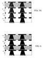
- FIGS. 4A and 4Bare schematic representations of a multilayer circuitized structure including high k ceramic particles incorporated into an organic layer, or deposited as a film, in accordance with an embodiment of the present invention.
- FIGS. 5A and 5Bare schematic representations of a multilayer circuitized structure including resistive particles incorporated into an organic layer, or deposited as a resistive film, in accordance with an embodiment of the present invention.
- FIG. 6is a schematic representation of a metalized circuitized structure including high k ceramic particles incorporated into the organic layer or deposited as a film on the organic layer, and a second organic layer including resistive particles incorporated into the second organic layer or deposited as a film on the second organic layer in accordance with an embodiment of the present invention.
- FIG. 7is a schematic representation of a multilayer circuitized structure including layers filled with high k ceramic and resistive particles and/or films deposited with high k ceramic and resistive particles, and a rigidizer layer in accordance with an embodiment of the present invention.
- FIG. 8is a schematic representation of a multilayer circuitized structure illustrating various packaging formats compatible with the present invention.
- the present inventioncomprises three-dimensional (3-D) multilayer structures having at least one low temperature organic layer and at least one high temperature organic layer that are processed in a parallel fashion that provides for individual layers to be independently fabricated and tested prior to lamination into a multilayer 3-D circuit.
- Metal to metal bondingis formed by incorporating a high temperature alloy that melts at a temperature slightly above the fusion point of the low temperature organic layer, but lower in temperature than the high melt point organic layer.
- the organic layer or materialmay comprise any low cost, high performance organic material, such as polyphenyl ether (PPE) based materials, such as LD621 from Polyclad and N6000 series from Park/Nelco Corporation, Teflon organic from Rogers Corporation, or liquid crystalline polymer (LCP), such as LCP from Rogers Corporation or W.L. Gore & Associates, Inc.
- PPEpolyphenyl ether
- LCPliquid crystalline polymer
- the construction of the circuits of the present inventiondoes not require an adhesive or lower melting point dielectric to form the 3-D interconnect.
- adhesiveswhich are typically epoxies or polyimides
- the multilayer 3-D circuits of the present inventionare homogeneous (e.g., where the two organic materials have the same thickness, dielectric constant, loss tangent, volume resistivity, matching coefficient of thermal expansion (CTE), and modulus) which is highly desirable for improved performance and design ease in high speed digital and high frequency RF/wireless applications both from an electrical standpoint and mechanical standpoint (e.g., to minimize warpage).
- the homogeneous constructionprovides smoother transitions and signal propagation in the z-axis direction, and facilitates the design of matched impedance networks since the dielectric constant and loss are the same, layer to layer.
- the present inventionincludes the incorporation of high k and resistive particles in the organic layers and/or the deposition of high k and resistive films, which represents additional advantages in design flexibility in realizing RE circuits that require RC, LC, and RLC networks.
- filters, couplers, duplexers, baluns, mixers, etc.can be integrally fabricated.
- Such structuresare possible because the host matrix material (e.g., filled LCP) is the same as the insulating low temperature and high temperature dielectrics.
- the low and/or high temperature LCP layereither can be filled with high k dielectric particles or incorporate a high k deposited thin film, which then can be incorporated into the circuit to form embedded decoupling, bandpass filters, low pass filters, baluns, couplers, etc., and baseband circuits such as capacitors, blocking filters, etc.
- Incorporation of the high k particlesmay be achieved by introducing a surfactant onto high k particles, such as Barium titinate, lead magnesium nitrate or titatium dioxide to minimize particle clustering, followed by drying and then subsequent introduction in the organic melt prior to drawing and pressing the cladded organic layer into finished sheets.
- the resultant high k layers sandwiched between copper sheets or planescan serve as embedded decoupling layers that can be processed in the multilayer stack for noise suppression and other benefits.
- the amount of high k particle incorporated into the organic layerwill determine the resultant dielectric constant values and mechanical integrity. Typical volume fraction will vary from 10% to 50%.
- high k organic layers that are either deposited or filledenable passive components and arrays that can support applications beyond 6 GHz, and are process compatible for the 3-D multilayer build up described herein. This is achieved, at least in part, by lithographically defining the top and bottom conductor layers to form a parallel plate construction. The filled organic as well as the non-filled organic is sandwich between the lithographically defined top and bottom conductor layers.
- the present inventionalso provides for the incorporation of resistive particles in the organic laminates or the deposition of resistive thin films on organic laminates, which enables passive components and arrays that provide for the formation of RC, and RLC networks.
- the resistive particlesmay include, for example, carbon, silicon carbide, rhuthenium oxide, copper, silver, or combinations thereof, that can be incorporated into the organic melt up to 50% volume, while resistive thin films could include NiP, TaN, NiCr, NiWP, ZnO, etc.
- a resistive circuitis completed upon deposition and circuitization of metal contacts to form terminals, thereby forming planar and annular resistors and resistor networks.
- resistor networksare formed by plating, sputtering, evaporating or chemical vapor deposition of metals and/or metallic alloys on finished organic laminates to form low and high value resistors and resistor networks upon circuitization of metallic terminals to form planar and annular resistors and resistor networks.
- the resistor devices or elementscan also be fabricated by laminating, electroplating, vacuum deposition, or printing of resistive films on the organic laminates. Upon putting down the resistive film, a metallic layer is deposited on the resistive film and the resistor and/or resistor networks are defined via a print and etch technique.
- the filled organic layersare metallized either by plating, lamination or vacuum deposition. The conductors can then be lithographically defined to form the metallic terminals of the resistors.
- the thin film of high k or resistive materialcan be fabricated on an organic layer using known techniques. For example, a layer of high k material can be deposited by CVD or sputtering and then lithographically defined into a desired design. Likewise, a layer of resistive material can be deposited by evaporation, CVS or sputtering and then lithographically defined. In either case, the thickness of the thin film will vary based upon the desired performance characteristics sought.
- a 3-D multilayer circuit in accordance with the present inventioncan be fabricated in either sequential mode or reel to reel.
- a sequential modea high temperature uncladded or single sided organic laminate from 1-10 mils in thickness is initially obtained.
- one sideis metallized by, for example, sputtering or chemical-electro deposition of a thin conductive film, such as copper, nickel or gold.
- the other sideis then drilled to form a via that terminates at the polymer-metal interface.
- the viais then metallized by electroless plating and capped with an adhesive metal, such as gold-tin.
- the bottom layerwhich served as the conductive layer or bus layer, is then circuitized to form a single metal layer circuit.
- other layerse.g., alternating layers of high and low melting point material
- the layersare stacked in a lamination press, whose temperature and pressure conditions will vary due to a number of known factors, such as the number of layers and the adhesive metal composition.
- the layersmay be laminated together in a press applying 75-500 psi at 270-280° C. for 5-20 minutes. Within this stack could be one or more high k dielectric layers and resistive layers.
- the stackis taken up in temperature and pressure and laminated to fuse the low temperature dielectric to the high temperature dielectric, the low temperature dielectric to the metal, and the metal alloy to the trace metal on the organic layer.
- the 3-D) metal layer circuitcan also be processed onto an expansion matched CTE (coefficient of thermal expansion) core or substrate.
- the core material and the dielectric materialcan be tailored to have the same thermal expansivity, which provides for little to no warpage for improved reliability.
- the CTE match of core and dielectriccan be tailored to that of silicon devices, which can be subsequently joined to the 3-D interconnect in the absence of underfill.
- FIG. 1Ais a schematic representation of an uncladded high temperature or low temperature LCP dielectric film 12 , in accordance with an embodiment of the present invention.
- the high and low temperature LCP filmhas a CTE between 2 and 20 ppm/° C.
- a metalized layer 14has been fabricated on the high temperature or low temperature LCP dielectric film 12 , in accordance with an embodiment of the present invention.
- Metallization of the LCP film 12can be accomplished by electroless and electroplating, sputtering, evaporation, or chemical vapor deposition.
- Metallizationcan be an adhesive metal such as copper, chromium, titanium, or platinum, followed by deposition of either copper, nickel, gold, or palladium.
- the thicknessis preferably between 0.5 microns to 200 microns.
- the high temperature or low temperature LCP dielectric film 12that has been drilled either by laser, mechanical, punch, etch, reactive ion etch to form vias 16 down to the underside of the metallization.
- Suitable lasersinclude UV, CO2, excinor, or YAG, and the drilling can be accomplished using computer numeric control (CNC) or using a patterned mask for image transfer.
- the metallized vias 16have been plated, sputtered, or filled with conductive paste or evaporated, to form a conductive via stud 18 within the via 16 , followed by the fabrication of an adhesive capping layer 20 , which comprises a high melting point alloy that forms metal to metal joining.
- the solid via studs 18form the z-axis interconnect between the layer of the stack up, while the adhesive caps 20 serve to form the reliable metal to interconnect bond.
- the capis preferably a metallic solder of a binary alloy that melts at a temperature above that of the fusion point of the high temperature and low temperature LCP layers.
- the metalized layer 14 fabricatede.g., printed and etched to form a single sided circuit layer
- the metalized layer 14 fabricatede.g., printed and etched to form a single sided circuit layer
- the metalized layer 14 fabricatede.g., printed and etched to form a single sided circuit layer
- circuitizede.g., etched
- Circuitization of the LCP sheetscan also be accomplished in an additive or semi additive method, where the defined circuit layer is formed by plating through a patterned photoresist.
- stripping of the resistand removal of the conductive bus layer used for the electroplating.
- FIG. 2is a schematic representation of multiple circuitized layers that have been stacked in an alternating sequences of aligned high temperature circuitized dielectric layers 24 and low temperature circuitized dielectric layers 26 , which are fusion bonded at temperatures and pressures sufficient enough to form a multilayer flex circuit construction, in accordance with an embodiment of the present invention.
- FIG. 3is a schematic representation of circuitized layers that have been stacked in alternating sequences of high temperature circuitized dielectric layers 24 and low temperature circuitized dielectric layers 26 with a matched coefficient of thermal expansion (CTE) rigidizer 30 , which can be either metallic or other inorganic, and which is fusion bonded to form a multilayer rigid circuit construction.
- the rigidizercan be disposed above or below the circuitized layers, as shown, or alternatively, the rigidizer can be aligned and placed between circuitized layers, where the circuit layers are stacked on either side of the rigidizer, followed by lamination of the entire stack up to form a multilayer rigidized circuit construction.
- the rigidizercan also serve as a heat sink, ground or power plane, or EMI shielding. Examples of suitable materials include copper-invar-copper (CIC) or aluminum silicon carbide.
- FIG. 4Ais a schematic representation of circuitized layers that have been stacked in alternating sequences of high temperature circuitized dielectric layers 24 and low temperature circuitized dielectric layers 26 with an LCP layer 40 filled with high k ceramic particles.
- a high k film 40 ′can be deposited on LCP layer, as shown in FIG. 4B .
- the LCP layer 40is fusion bonded in the multilayer stackup and circuitized to form a multilayer flex circuit construction with embedded inductors and capacitors in accordance with an embodiment of the present invention.
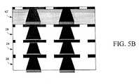
- FIG. 5Ais a schematic representation of circuitized layers that have been stacked in alternating sequences of high temperature circuitized dielectric layers 24 and low temperature circuitized dielectric layers 26 with an LCP film 42 filled with resistive particles.
- a resistive films 42 ′such as NiCr, TaN, NiP, or NiWP
- the LCP layeris fusion bonded to form a multilayer flex circuit construction with embedded resistors (R), inductors (L) and capacitors (C).
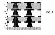
- FIG. 6is a schematic representation of circuitized layers that have been stacked in alternating sequences of high temperature circuitized dielectric layers 24 and low temperature circuitized dielectric layers 26 that includes a layer 44 that includes a deposited high k dielectric film or is LCP filled with high k ceramic particles, and in a separate discrete level of the stack, a layer 46 that includes a deposited resistive film 46 or is filled LCP with resistive particles, wherein the stack is fusion bonded to form a multilayer flex circuit construction with embedded R, L and C's.
- FIG. 7is a schematic representation of a rigid multilayer circuit of FIG. 6 with a metallic, inorganic or organic rigidizer 50 .
- the rigidizer 50can be located on either side of the multilayer circuit stackup or within the multilayer stack up to form a rigid multilayer circuit construction with embedded components such as R, L, and C's. Through vias that arc filled with plated copper or conductor paste can be used to connect circuit layers on opposite sides of the rigidizer.
- the multilayer substrate or modulecan be used for interconnecting a vast array of active and passive components either through direct attached methods or surface mount technologies.
- the multilayer 3D interconnect structure described hereincan support the packaging and interconnection of various active and passive components in addition to the passive components embedded in the structure to form functional modules or system boards for digital, RF/wireless, or mixed signal modules.
- the ability to tailor the expansion of the multilayer circuit, described above,enables the packaging of different active chips such as silicon CMOS, Sol, SiGe, GaAs, and surface mount passive components in a highly reliable platform.
- FIG. 8is a schematic representation of a multilayer circuitized structure including various illustrative packaging formats supported by the present invention. Suitable packaging formats include, but are not limited to, flip-chip, wafer level packages (WLP), chip scale packages (CSP), ball grid array (BGA), wire bonded devices and various surface mount devices (SMD or SMT).
- the formats illustrated in FIG. 8include cavity flip chip or wirebond 70 , flip chip wafer level packaging 72 , BGA/CSP 74 , SMD/SMT 76 and wire bond 78 .
- the chips and/or package components 80can be attached on a top surface of the multilayer circuit or within cavities formed inside the multilayer circuit using routing, punching, laser machining or other standard processes known to those skilled in the art. These cavities can be single level or multilevel and can be interconnected to other circuit layers using microvias or plated through holes.
- the packaged components 80 on the top side of the module or in cavitiescan be interconnected to each other, to the embedded passive layers that include capacitors, inductors, resistors, etc., or to the BGA pads 80 on the bottom side of the module.
- the side walls of the module substratecan be covered with conductor like Cu, Ni, Au or other absorbing materials to provide shielding from EMI and other external radiation. This shielding can be formed with electroless and electroplating, vacuum deposition, lamination or other deposition methods known to those skilled in the art.
- the assembled multilayer module substratecan form a system board for a system or can be terminated with ball grid array on the bottom side or wirebonded from the top side for further interconnection to other components on a system board.
Landscapes
- Engineering & Computer Science (AREA)
- Microelectronics & Electronic Packaging (AREA)
- Power Engineering (AREA)
- Manufacturing & Machinery (AREA)
- Physics & Mathematics (AREA)
- Condensed Matter Physics & Semiconductors (AREA)
- General Physics & Mathematics (AREA)
- Computer Hardware Design (AREA)
- Ceramic Engineering (AREA)
- Production Of Multi-Layered Print Wiring Board (AREA)
- Parts Printed On Printed Circuit Boards (AREA)
- Laminated Bodies (AREA)
Abstract
Description
- This application is a continuation of U.S. application Ser. No. 10/402,315, filed Mar. 28, 2003. In addition, this application is related to the following commonly assigned U.S. applications: “Integrated Passive Devices Fabricated Utilizing Multilayer, Organic Laminates” filed Mar. 28, 2003, and accorded application Ser. No. 10/402,313, which issued on May 31, 2005 as U.S. Pat. No. 6,900,708; “Stand-Alone Organic-Based Passive Devices” filed Mar. 28, 2003, and accorded application Ser. No. 10/405,024, which issued on Jan. 17, 2006 as U.S. Pat. No. 6,987,307; and “Integrated Passive Devices Fabricated Utilizing Multilayer, Organic Laminates,” filed May 27, 2005, and accorded application Ser. No. 11/140,630, which issued on Jun. 27, 2006 as U.S. Pat. No. 7,068,124.
- I. Field of the Invention
- The present invention generally relates to three-dimensional all organic structures, and more particularly to three-dimensional organic interconnect structures for use in radio frequency and mixed signal module substrates and multilayer high-speed printed circuit boards.
- II. Description of Related Art
- Multilayer circuits typically comprise at least one conductive circuit layer bonded or laminated to a dielectric layer. The conductive circuit layer is generally a conductive metal such as copper, and the dielectric layer generally comprises a polymer resin such as epoxy. Depending on the selection of the dielectric layer and its thickness, the circuit can be either stiff or flexible.
- Multilayer organic circuits incorporating thin film technologies are typically fabricated by parallel processing using diclad or monoclad layers that are sandwiched between bond ply materials to form a multilayer circuit construction. The number of metal layers can be as few as two and as many as sixty or more. The requirements for multilayer circuits in high density, high performance applications are becoming ever more demanding for high frequency applications. As a result there exists an unresolved need for a low cost multilayer process that can support both high frequency and high density (e.g., fine line and spaces, small via sizes) multilayer circuit constructions.
- The present invention comprises three-dimensional (3-D) multilayer circuit structures and methods of fabricating same wherein the circuit structures comprise uncladded high and low temperature organic material, such as liquid crystalline polymers (LCPs), teflon or polyphenyl ether (PPE) based materials, that have equivalent electrical and mechanical properties but differing melt temperatures, which enable a uniform homogeneous electrical circuit that can support high frequency and high bandwidth applications. The two different melt points allow for the stacking and lamination of individual circuitized layers to form multilayer construction, which when combined with a higher temperature metallic alloy provides for a reliable metal to metal joining that occurs at a temperature slightly above that at which the fusion bonding of the dielectric to dielectric and dielectric to metal occurs. Incorporation of resistive and high k particles or deposition resistive and high k films into or onto the high melt point and/or low melt point organic layers allows for the ability to integrate buried passives structures, (e.g., bias, decoupling and filter elements) in a 3-D multilayer construction.
- The incorporation or deposition of the resistive materials into or on the organic layers provides for the ability to form single resistor elements and arrays when combined with a standardized lithographical process for circuit formation. Similarly, the incorporation of high dielectric constant materials or deposition of the same having dielectric constants from 8 to 20,000 provides for single capacitor elements and arrays when combined with standardized lithographical processes for circuit formation. This enables the fabrication of parallel plate capacitors, inter-digitated (comb) capacitors and distributed capacitance layers with capacitance densities well beyond 1 nf/cm2.
- The use of uncladded high temperature and low temperature organic layers allow for the fabrication of fine line geometries down to five micron lines and spaces using build up processes that involve depositing a thin metal conductive layer by electroless plating or vacuum deposition, which could be any one of copper, Ni, Au, Pd, Pt. A photoresist is then deposited, lithographically exposed and then developed. A conductor metal layer is then electroplating through the patterned resist, wherein the conductor metal could be any one of Cu, Ni, Au, Pd, or Pt. While the resist is still in place, an adhesive metal is plated on the previous conductor metal layer. The adhesive metal may be any one of a number of high temperature alloys that will bond at temperatures exceeding the softening point of the organic layers. Such alloys may include, AuSn, PdSn, NiSn.
- The various layers can be selectively interconnected by small via (also referred to herein as z-axis interconnects or studs) formed in the organic layers at the dimensions down to ten micron using laser or reactive ion etch techniques. Single side copper formation on the underside of the LCP layer serves as a stop during via formation using a laser or mechanical drill. The underside copper also serves as a cathode or bus layer to provide for the formation of the z-axis interconnect or metallic stud to form a 3-D interconnect structure. The studs or z-axis interconnects are formed by electroplating either copper, nickel, gold, silver or similar conductive metal. The use of electroplating allows for solid via stud formation for improved conductivity.
- After fabrication of the conductive metal stud within an organic layer, the top of the stud is capped with high melting point metallic alloy that bonds to copper (or other metallic conductor material used) to form 3-D interconnection upon lamination of high temperature and low temperature metallized organic layer, such as an LCP or similar organic material layer.
- Having thus described the invention in general terms, reference will now be made to the accompanying drawings, which are not necessarily drawn to scale, and wherein:
FIGS. 1A-1E are schematic representations of the incremental steps in the fabrication of a multilayer structure in accordance with an embodiment of the present invention.FIG. 2 is a schematic representation of multiple circuitized layers stacked in an alternating sequence of high and low temperature dielectrics.FIG. 3 is a schematic representation of a multilayer circuitized structure including an expansion matched rigidizer embodiment of the present invention.FIGS. 4A and 4B are schematic representations of a multilayer circuitized structure including high k ceramic particles incorporated into an organic layer, or deposited as a film, in accordance with an embodiment of the present invention.FIGS. 5A and 5B are schematic representations of a multilayer circuitized structure including resistive particles incorporated into an organic layer, or deposited as a resistive film, in accordance with an embodiment of the present invention.FIG. 6 is a schematic representation of a metalized circuitized structure including high k ceramic particles incorporated into the organic layer or deposited as a film on the organic layer, and a second organic layer including resistive particles incorporated into the second organic layer or deposited as a film on the second organic layer in accordance with an embodiment of the present invention.FIG. 7 is a schematic representation of a multilayer circuitized structure including layers filled with high k ceramic and resistive particles and/or films deposited with high k ceramic and resistive particles, and a rigidizer layer in accordance with an embodiment of the present invention.FIG. 8 is a schematic representation of a multilayer circuitized structure illustrating various packaging formats compatible with the present invention.- The present inventions now will be described more fully hereinafter with reference to the accompanying drawings, in which some, but not all embodiments of the invention are shown. Indeed, these inventions may be embodied in many different forms and should not be construed as limited to the embodiments set forth herein; rather, these embodiments are provided so that this disclosure will satisfy applicable legal requirements. Like numbers refer to like elements throughout.
- The present invention comprises three-dimensional (3-D) multilayer structures having at least one low temperature organic layer and at least one high temperature organic layer that are processed in a parallel fashion that provides for individual layers to be independently fabricated and tested prior to lamination into a multilayer 3-D circuit. Metal to metal bonding is formed by incorporating a high temperature alloy that melts at a temperature slightly above the fusion point of the low temperature organic layer, but lower in temperature than the high melt point organic layer.
- For purposes of the present invention, the organic layer or material may comprise any low cost, high performance organic material, such as polyphenyl ether (PPE) based materials, such as LD621 from Polyclad and N6000 series from Park/Nelco Corporation, Teflon organic from Rogers Corporation, or liquid crystalline polymer (LCP), such as LCP from Rogers Corporation or W.L. Gore & Associates, Inc. These materials provide excellent hermicity and temperature independence, which emulates the performance of ceramic substrates used to construct multilayer ceramic structures.
- Advantageously, the construction of the circuits of the present invention does not require an adhesive or lower melting point dielectric to form the 3-D interconnect. As is known to those skilled in the art, adhesives (which are typically epoxies or polyimides) have dissimilar electrical and mechanical properties that are susceptible to moisture uptake, which degrades performance. In addition, the multilayer 3-D circuits of the present invention are homogeneous (e.g., where the two organic materials have the same thickness, dielectric constant, loss tangent, volume resistivity, matching coefficient of thermal expansion (CTE), and modulus) which is highly desirable for improved performance and design ease in high speed digital and high frequency RF/wireless applications both from an electrical standpoint and mechanical standpoint (e.g., to minimize warpage). From an electrical standpoint, the homogeneous construction provides smoother transitions and signal propagation in the z-axis direction, and facilitates the design of matched impedance networks since the dielectric constant and loss are the same, layer to layer.
- The present invention includes the incorporation of high k and resistive particles in the organic layers and/or the deposition of high k and resistive films, which represents additional advantages in design flexibility in realizing RE circuits that require RC, LC, and RLC networks. Thus, filters, couplers, duplexers, baluns, mixers, etc. can be integrally fabricated. Such structures are possible because the host matrix material (e.g., filled LCP) is the same as the insulating low temperature and high temperature dielectrics. The low and/or high temperature LCP layer either can be filled with high k dielectric particles or incorporate a high k deposited thin film, which then can be incorporated into the circuit to form embedded decoupling, bandpass filters, low pass filters, baluns, couplers, etc., and baseband circuits such as capacitors, blocking filters, etc. Incorporation of the high k particles may be achieved by introducing a surfactant onto high k particles, such as Barium titinate, lead magnesium nitrate or titatium dioxide to minimize particle clustering, followed by drying and then subsequent introduction in the organic melt prior to drawing and pressing the cladded organic layer into finished sheets. The resultant high k layers sandwiched between copper sheets or planes can serve as embedded decoupling layers that can be processed in the multilayer stack for noise suppression and other benefits. The amount of high k particle incorporated into the organic layer will determine the resultant dielectric constant values and mechanical integrity. Typical volume fraction will vary from 10% to 50%. Additionally, high k organic layers that are either deposited or filled enable passive components and arrays that can support applications beyond 6 GHz, and are process compatible for the 3-D multilayer build up described herein. This is achieved, at least in part, by lithographically defining the top and bottom conductor layers to form a parallel plate construction. The filled organic as well as the non-filled organic is sandwich between the lithographically defined top and bottom conductor layers.
- The present invention also provides for the incorporation of resistive particles in the organic laminates or the deposition of resistive thin films on organic laminates, which enables passive components and arrays that provide for the formation of RC, and RLC networks. The resistive particles may include, for example, carbon, silicon carbide, rhuthenium oxide, copper, silver, or combinations thereof, that can be incorporated into the organic melt up to 50% volume, while resistive thin films could include NiP, TaN, NiCr, NiWP, ZnO, etc. A resistive circuit is completed upon deposition and circuitization of metal contacts to form terminals, thereby forming planar and annular resistors and resistor networks. In addition, resistor networks are formed by plating, sputtering, evaporating or chemical vapor deposition of metals and/or metallic alloys on finished organic laminates to form low and high value resistors and resistor networks upon circuitization of metallic terminals to form planar and annular resistors and resistor networks. The resistor devices or elements can also be fabricated by laminating, electroplating, vacuum deposition, or printing of resistive films on the organic laminates. Upon putting down the resistive film, a metallic layer is deposited on the resistive film and the resistor and/or resistor networks are defined via a print and etch technique. In defining resistors or resistive networks using filled resistive organic layers, the filled organic layers are metallized either by plating, lamination or vacuum deposition. The conductors can then be lithographically defined to form the metallic terminals of the resistors.
- The thin film of high k or resistive material can be fabricated on an organic layer using known techniques. For example, a layer of high k material can be deposited by CVD or sputtering and then lithographically defined into a desired design. Likewise, a layer of resistive material can be deposited by evaporation, CVS or sputtering and then lithographically defined. In either case, the thickness of the thin film will vary based upon the desired performance characteristics sought.
- A 3-D multilayer circuit in accordance with the present invention can be fabricated in either sequential mode or reel to reel. In a sequential mode, a high temperature uncladded or single sided organic laminate from 1-10 mils in thickness is initially obtained. For the uncladded example, one side is metallized by, for example, sputtering or chemical-electro deposition of a thin conductive film, such as copper, nickel or gold. The other side is then drilled to form a via that terminates at the polymer-metal interface. Upon appropriate surface treatment (e.g., by plasma or chemical etching), the via is then metallized by electroless plating and capped with an adhesive metal, such as gold-tin. The bottom layer, which served as the conductive layer or bus layer, is then circuitized to form a single metal layer circuit. Upon completion of the circuit, other layers (e.g., alternating layers of high and low melting point material) are combined so that 3-D connections are formed by the vias h/l stackup. The layers are stacked in a lamination press, whose temperature and pressure conditions will vary due to a number of known factors, such as the number of layers and the adhesive metal composition. As an example, the layers may be laminated together in a press applying 75-500 psi at 270-280° C. for 5-20 minutes. Within this stack could be one or more high k dielectric layers and resistive layers. The stack is taken up in temperature and pressure and laminated to fuse the low temperature dielectric to the high temperature dielectric, the low temperature dielectric to the metal, and the metal alloy to the trace metal on the organic layer.
- The 3-D) metal layer circuit can also be processed onto an expansion matched CTE (coefficient of thermal expansion) core or substrate. The core material and the dielectric material can be tailored to have the same thermal expansivity, which provides for little to no warpage for improved reliability. In addition, the CTE match of core and dielectric can be tailored to that of silicon devices, which can be subsequently joined to the 3-D interconnect in the absence of underfill.
- Illustrative Embodiments
- The following is an illustrative embodiment of a method of fabricating a multilaver organic structure according to the present invention utilizing LCP as the organic material, followed by several alternative embodiments.
FIG. 1A is a schematic representation of an uncladded high temperature or low temperatureLCP dielectric film 12, in accordance with an embodiment of the present invention. In a preferred embodiment, the high and low temperature LCP film has a CTE between 2 and 20 ppm/° C.- Next, as illustrated in
FIG. 1B , ametalized layer 14 has been fabricated on the high temperature or low temperatureLCP dielectric film 12, in accordance with an embodiment of the present invention. Metallization of theLCP film 12 can be accomplished by electroless and electroplating, sputtering, evaporation, or chemical vapor deposition. Metallization can be an adhesive metal such as copper, chromium, titanium, or platinum, followed by deposition of either copper, nickel, gold, or palladium. The thickness is preferably between 0.5 microns to 200 microns. - Next, as illustrated in
FIG. 1C , the high temperature or low temperatureLCP dielectric film 12 that has been drilled either by laser, mechanical, punch, etch, reactive ion etch to formvias 16 down to the underside of the metallization. Suitable lasers include UV, CO2, excinor, or YAG, and the drilling can be accomplished using computer numeric control (CNC) or using a patterned mask for image transfer. - As illustrated in
FIG. 1D , the metallizedvias 16 have been plated, sputtered, or filled with conductive paste or evaporated, to form a conductive viastud 18 within the via16, followed by the fabrication of anadhesive capping layer 20, which comprises a high melting point alloy that forms metal to metal joining. The solid viastuds 18 form the z-axis interconnect between the layer of the stack up, while theadhesive caps 20 serve to form the reliable metal to interconnect bond. The cap is preferably a metallic solder of a binary alloy that melts at a temperature above that of the fusion point of the high temperature and low temperature LCP layers. - Next, as illustrated in
FIG. 1E , the metalizedlayer 14 fabricated (e.g., printed and etched to form a single sided circuit layer) on either a high temperature or low temperatureLCP dielectric film 12 is circuitized (e.g., etched). Circuitization of the LCP sheets can also be accomplished in an additive or semi additive method, where the defined circuit layer is formed by plating through a patterned photoresist. Followed by stripping of the resist and removal of the conductive bus layer used for the electroplating. FIG. 2 is a schematic representation of multiple circuitized layers that have been stacked in an alternating sequences of aligned high temperature circuitized dielectric layers24 and low temperature circuitized dielectric layers26, which are fusion bonded at temperatures and pressures sufficient enough to form a multilayer flex circuit construction, in accordance with an embodiment of the present invention.FIG. 3 is a schematic representation of circuitized layers that have been stacked in alternating sequences of high temperature circuitized dielectric layers24 and low temperature circuitized dielectric layers26 with a matched coefficient of thermal expansion (CTE) rigidizer30, which can be either metallic or other inorganic, and which is fusion bonded to form a multilayer rigid circuit construction. The rigidizer can be disposed above or below the circuitized layers, as shown, or alternatively, the rigidizer can be aligned and placed between circuitized layers, where the circuit layers are stacked on either side of the rigidizer, followed by lamination of the entire stack up to form a multilayer rigidized circuit construction. Depending on the material comprising the rigidizer, it can also serve as a heat sink, ground or power plane, or EMI shielding. Examples of suitable materials include copper-invar-copper (CIC) or aluminum silicon carbide.FIG. 4A is a schematic representation of circuitized layers that have been stacked in alternating sequences of high temperature circuitized dielectric layers24 and low temperature circuitized dielectric layers26 with anLCP layer 40 filled with high k ceramic particles. Alternatively, ahigh k film 40′ can be deposited on LCP layer, as shown inFIG. 4B . TheLCP layer 40 is fusion bonded in the multilayer stackup and circuitized to form a multilayer flex circuit construction with embedded inductors and capacitors in accordance with an embodiment of the present invention.FIG. 5A is a schematic representation of circuitized layers that have been stacked in alternating sequences of high temperature circuitized dielectric layers24 and low temperature circuitized dielectric layers26 with anLCP film 42 filled with resistive particles. Alternatively, aresistive films 42′ (such as NiCr, TaN, NiP, or NiWP) can be deposited on the LCP layer as illustrated inFIG. 5B . The LCP layer is fusion bonded to form a multilayer flex circuit construction with embedded resistors (R), inductors (L) and capacitors (C).FIG. 6 is a schematic representation of circuitized layers that have been stacked in alternating sequences of high temperature circuitized dielectric layers24 and low temperature circuitized dielectric layers26 that includes alayer 44 that includes a deposited high k dielectric film or is LCP filled with high k ceramic particles, and in a separate discrete level of the stack, alayer 46 that includes a depositedresistive film 46 or is filled LCP with resistive particles, wherein the stack is fusion bonded to form a multilayer flex circuit construction with embedded R, L and C's.FIG. 7 is a schematic representation of a rigid multilayer circuit ofFIG. 6 with a metallic, inorganic ororganic rigidizer 50. Therigidizer 50 can be located on either side of the multilayer circuit stackup or within the multilayer stack up to form a rigid multilayer circuit construction with embedded components such as R, L, and C's. Through vias that arc filled with plated copper or conductor paste can be used to connect circuit layers on opposite sides of the rigidizer. The multilayer substrate or module can be used for interconnecting a vast array of active and passive components either through direct attached methods or surface mount technologies.- The multilayer 3D interconnect structure described herein can support the packaging and interconnection of various active and passive components in addition to the passive components embedded in the structure to form functional modules or system boards for digital, RF/wireless, or mixed signal modules. The ability to tailor the expansion of the multilayer circuit, described above, enables the packaging of different active chips such as silicon CMOS, Sol, SiGe, GaAs, and surface mount passive components in a highly reliable platform. For example,
FIG. 8 is a schematic representation of a multilayer circuitized structure including various illustrative packaging formats supported by the present invention. Suitable packaging formats include, but are not limited to, flip-chip, wafer level packages (WLP), chip scale packages (CSP), ball grid array (BGA), wire bonded devices and various surface mount devices (SMD or SMT). - The formats illustrated in
FIG. 8 include cavity flip chip orwirebond 70, flip chipwafer level packaging 72, BGA/CSP 74, SMD/SMT 76 andwire bond 78. The chips and/orpackage components 80 can be attached on a top surface of the multilayer circuit or within cavities formed inside the multilayer circuit using routing, punching, laser machining or other standard processes known to those skilled in the art. These cavities can be single level or multilevel and can be interconnected to other circuit layers using microvias or plated through holes. Usingmicrovias 82 and plated throughholes 84, the packagedcomponents 80 on the top side of the module or in cavities can be interconnected to each other, to the embedded passive layers that include capacitors, inductors, resistors, etc., or to theBGA pads 80 on the bottom side of the module. The side walls of the module substrate can be covered with conductor like Cu, Ni, Au or other absorbing materials to provide shielding from EMI and other external radiation. This shielding can be formed with electroless and electroplating, vacuum deposition, lamination or other deposition methods known to those skilled in the art. The assembled multilayer module substrate can form a system board for a system or can be terminated with ball grid array on the bottom side or wirebonded from the top side for further interconnection to other components on a system board. - Many modifications and other embodiments of the inventions set forth herein will come to mind to one skilled in the art to which these inventions pertain having the benefit of the teachings presented in the foregoing descriptions and the associated drawings. Therefore, it is to be understood that the inventions are not to be limited to the specific embodiments disclosed and that modifications and other embodiments are intended to be included within the scope of the appended claims. Although specific terms are employed herein, they are used in a generic and descriptive sense only and not for purposes of limitation.
Claims (20)
1. A method of fabricating 3-D multi layer interconnect structures, comprising:
providing a first organic layer of a first melting point having a first single sided circuitized conductive layer;
providing a second organic layer of a second melting point having a second single sided circuitized conductive layer and including at least one metal filled z-axis via connection stud, wherein the first and second melting points are different; and
bonding the first organic layer to the second organic layer,
wherein the first organic layer having the first single-sided circuitized conductive layer and the second organic layer having the second single-sided circuitized layer are provided prior to the step of bonding,
wherein the first organic layer forms a fusion bond with the second organic layer, and the z-axis stud of the second organic layer forms a metal to metal bond with the first conductive layer, and wherein the first and second organic layers remain substantially the same prior to and subsequent to the step of bonding.
2. The method ofclaim 1 , wherein the first or second conductive layer comprises at least one of copper, aluminum, gold, nickel, iron, silver, zinc, chromium and a combination thereof.
3. The method ofclaim 1 , wherein at least one conductive layer on one of the first and second organic layers serves as a bus layer prior to the z-axis via stud formation.
4. The method ofclaim 1 , wherein the first melting point is less than the second melting point.
5. The method ofclaim 1 , wherein the first melting point is greater than the second melting point.
6. The method ofclaim 1 , wherein the first conductive layer has a thickness from approximately 0.5 microns to 200 microns.
7. The method ofclaim 1 , wherein the first and second organic layers are laminated together in a stack to form a three-dimensional (3-D) circuit.
8. The method ofclaim 7 , wherein the 3-D circuit is a flexible circuit.
9. The method ofclaim 7 , wherein the 3-D circuit is a rigid circuit.
10. The method ofclaim 7 , wherein the coefficient of thermal expansion of the completed 3-D circuit in the x and y directions are substantially matched.
11. The method ofclaim 7 , wherein the coefficient of thermal expansion of the first and second organic layers is between 2 and 20 ppm° C.
12. The method ofclaim 1 , wherein the second organic layer is sufficiently filled with high k dielectric constant particles to achieve a suitable high k film for high value capacitors and resonator structures.
13. The method ofclaim 1 , wherein the second organic layer includes a thin film of high k dielectric constant material.
14. The method ofclaim 1 , wherein the second organic layer is sufficiently filled with resistive particles and circuitized to form a resistor or a resistor network.
15. The method ofclaim 1 , wherein the second organic layer includes a thin film of resistive material.
16. The method ofclaim 1 , further comprising an expansion matched core that is bonded to one of the first or second organic layers to provide expansion matching to one of an organic, ceramic, or metal substrate.
17. The method ofclaim 16 , wherein the expansion matched core is metallic, and performs thermal and electrical functions.
18. The method ofclaim 1 , wherein the first and second organic layers are homogenous in electrical and mechanical properties, excluding melting points.
19. The method ofclaim 1 , wherein the z-axis stud comprises a cap at an end of the z-axis stud, wherein the cap of the z-axis stud forms the metal to metal bond with the first conductive layer.
20. The method ofclaim 19 , wherein the cap is a metallic solder of a binary alloy that melts above a fusion point of the first and second organic layers.
Priority Applications (1)
| Application Number | Priority Date | Filing Date | Title |
|---|---|---|---|
| US11/833,626US7805834B2 (en) | 2003-03-28 | 2007-08-03 | Method for fabricating three-dimensional all organic interconnect structures |
Applications Claiming Priority (2)
| Application Number | Priority Date | Filing Date | Title |
|---|---|---|---|
| US10/402,315US7260890B2 (en) | 2002-06-26 | 2003-03-28 | Methods for fabricating three-dimensional all organic interconnect structures |
| US11/833,626US7805834B2 (en) | 2003-03-28 | 2007-08-03 | Method for fabricating three-dimensional all organic interconnect structures |
Related Parent Applications (1)
| Application Number | Title | Priority Date | Filing Date |
|---|---|---|---|
| US10/402,315ContinuationUS7260890B2 (en) | 2002-06-26 | 2003-03-28 | Methods for fabricating three-dimensional all organic interconnect structures |
Publications (2)
| Publication Number | Publication Date |
|---|---|
| US20070267138A1true US20070267138A1 (en) | 2007-11-22 |
| US7805834B2 US7805834B2 (en) | 2010-10-05 |
Family
ID=33130442
Family Applications (2)
| Application Number | Title | Priority Date | Filing Date |
|---|---|---|---|
| US10/402,315Expired - LifetimeUS7260890B2 (en) | 2002-06-26 | 2003-03-28 | Methods for fabricating three-dimensional all organic interconnect structures |
| US11/833,626Expired - LifetimeUS7805834B2 (en) | 2003-03-28 | 2007-08-03 | Method for fabricating three-dimensional all organic interconnect structures |
Family Applications Before (1)
| Application Number | Title | Priority Date | Filing Date |
|---|---|---|---|
| US10/402,315Expired - LifetimeUS7260890B2 (en) | 2002-06-26 | 2003-03-28 | Methods for fabricating three-dimensional all organic interconnect structures |
Country Status (5)
| Country | Link |
|---|---|
| US (2) | US7260890B2 (en) |
| EP (1) | EP1611611B1 (en) |
| JP (1) | JP4568718B2 (en) |
| KR (1) | KR101076061B1 (en) |
| WO (1) | WO2004088731A2 (en) |
Cited By (66)
| Publication number | Priority date | Publication date | Assignee | Title |
|---|---|---|---|---|
| US20020120854A1 (en)* | 2000-09-22 | 2002-08-29 | Levine Richard B. | Systems and methods for preventing unauthorized use of digital content |
| US20070199074A1 (en)* | 2000-09-22 | 2007-08-23 | Ecd Systems | Systems and methods for preventing unauthorized use of digital content |
| US7531453B2 (en) | 2004-06-29 | 2009-05-12 | Micron Technology, Inc. | Microelectronic devices and methods for forming interconnects in microelectronic devices |
| US20090151990A1 (en)* | 2007-06-14 | 2009-06-18 | Hitachi Cable, Ltd. | Multilayer wiring board and method of making the same |
| US7622377B2 (en) | 2005-09-01 | 2009-11-24 | Micron Technology, Inc. | Microfeature workpiece substrates having through-substrate vias, and associated methods of formation |
| US7629249B2 (en) | 2006-08-28 | 2009-12-08 | Micron Technology, Inc. | Microfeature workpieces having conductive interconnect structures formed by chemically reactive processes, and associated systems and methods |
| US20100059897A1 (en)* | 2008-09-11 | 2010-03-11 | Micron Technology, Inc. | Interconnect structures for stacked dies, including penetrating structures for through-silicon vias, and associated systems and methods |
| US7683458B2 (en) | 2004-09-02 | 2010-03-23 | Micron Technology, Inc. | Through-wafer interconnects for photoimager and memory wafers |
| US20100096759A1 (en)* | 2008-10-16 | 2010-04-22 | Micron Technology, Inc. | Semiconductor substrates with unitary vias and via terminals, and associated systems and methods |
| US7749899B2 (en) | 2006-06-01 | 2010-07-06 | Micron Technology, Inc. | Microelectronic workpieces and methods and systems for forming interconnects in microelectronic workpieces |
| US7759800B2 (en) | 2003-11-13 | 2010-07-20 | Micron Technology, Inc. | Microelectronics devices, having vias, and packaged microelectronic devices having vias |
| US7795134B2 (en) | 2005-06-28 | 2010-09-14 | Micron Technology, Inc. | Conductive interconnect structures and formation methods using supercritical fluids |
| US7830018B2 (en) | 2007-08-31 | 2010-11-09 | Micron Technology, Inc. | Partitioned through-layer via and associated systems and methods |
| US7863187B2 (en) | 2005-09-01 | 2011-01-04 | Micron Technology, Inc. | Microfeature workpieces and methods for forming interconnects in microfeature workpieces |
| US7884015B2 (en) | 2007-12-06 | 2011-02-08 | Micron Technology, Inc. | Methods for forming interconnects in microelectronic workpieces and microelectronic workpieces formed using such methods |
| US7902643B2 (en) | 2006-08-31 | 2011-03-08 | Micron Technology, Inc. | Microfeature workpieces having interconnects and conductive backplanes, and associated systems and methods |
| US7915736B2 (en) | 2005-09-01 | 2011-03-29 | Micron Technology, Inc. | Microfeature workpieces and methods for forming interconnects in microfeature workpieces |
| WO2011084216A3 (en)* | 2009-12-17 | 2011-09-09 | Intel Corporation | Substrate for integrated circuit devices including multi-layer glass core and methods of making the same |
| US20110247871A1 (en)* | 2010-04-12 | 2011-10-13 | Samsung Electronics Co., Ltd. | Multi-layer printed circuit board comprising film and method for fabricating the same |
| US8084866B2 (en) | 2003-12-10 | 2011-12-27 | Micron Technology, Inc. | Microelectronic devices and methods for filling vias in microelectronic devices |
| US8117667B2 (en) | 2001-05-09 | 2012-02-14 | Sca Ipla Holdings Inc. | Systems and methods for the prevention of unauthorized use and manipulation of digital content |
| US8322031B2 (en) | 2004-08-27 | 2012-12-04 | Micron Technology, Inc. | Method of manufacturing an interposer |
| US8536485B2 (en) | 2004-05-05 | 2013-09-17 | Micron Technology, Inc. | Systems and methods for forming apertures in microfeature workpieces |
| US8907447B2 (en) | 2010-02-19 | 2014-12-09 | Mingliang Wang | Power inductors in silicon |
| WO2015006393A1 (en) | 2013-07-11 | 2015-01-15 | Hsio Technologies, Llc | Fusion bonded liquid crystal polymer circuit structure |
| US8955215B2 (en) | 2009-05-28 | 2015-02-17 | Hsio Technologies, Llc | High performance surface mount electrical interconnect |
| US8970031B2 (en) | 2009-06-16 | 2015-03-03 | Hsio Technologies, Llc | Semiconductor die terminal |
| US8981809B2 (en) | 2009-06-29 | 2015-03-17 | Hsio Technologies, Llc | Compliant printed circuit semiconductor tester interface |
| US8984748B2 (en) | 2009-06-29 | 2015-03-24 | Hsio Technologies, Llc | Singulated semiconductor device separable electrical interconnect |
| US8988093B2 (en) | 2009-06-02 | 2015-03-24 | Hsio Technologies, Llc | Bumped semiconductor wafer or die level electrical interconnect |
| US9001520B2 (en) | 2012-09-24 | 2015-04-07 | Intel Corporation | Microelectronic structures having laminated or embedded glass routing structures for high density packaging |
| US9054097B2 (en) | 2009-06-02 | 2015-06-09 | Hsio Technologies, Llc | Compliant printed circuit area array semiconductor device package |
| US9076884B2 (en) | 2009-06-02 | 2015-07-07 | Hsio Technologies, Llc | Compliant printed circuit semiconductor package |
| US9093767B2 (en) | 2009-06-02 | 2015-07-28 | Hsio Technologies, Llc | High performance surface mount electrical interconnect |
| US9136196B2 (en) | 2009-06-02 | 2015-09-15 | Hsio Technologies, Llc | Compliant printed circuit wafer level semiconductor package |
| US9184527B2 (en) | 2009-06-02 | 2015-11-10 | Hsio Technologies, Llc | Electrical connector insulator housing |
| US9184145B2 (en) | 2009-06-02 | 2015-11-10 | Hsio Technologies, Llc | Semiconductor device package adapter |
| US9196980B2 (en) | 2009-06-02 | 2015-11-24 | Hsio Technologies, Llc | High performance surface mount electrical interconnect with external biased normal force loading |
| US9214391B2 (en) | 2004-12-30 | 2015-12-15 | Micron Technology, Inc. | Methods for forming interconnects in microelectronic workpieces and microelectronic workpieces formed using such methods |
| US9231328B2 (en) | 2009-06-02 | 2016-01-05 | Hsio Technologies, Llc | Resilient conductive electrical interconnect |
| US9232654B2 (en) | 2009-06-02 | 2016-01-05 | Hsio Technologies, Llc | High performance electrical circuit structure |
| US20160014908A1 (en)* | 2010-06-03 | 2016-01-14 | Hsio Technologies, Llc | Fusion bonded liquid crystal polymer circuit structure |
| US9276336B2 (en) | 2009-05-28 | 2016-03-01 | Hsio Technologies, Llc | Metalized pad to electrical contact interface |
| US9276339B2 (en) | 2009-06-02 | 2016-03-01 | Hsio Technologies, Llc | Electrical interconnect IC device socket |
| US9277654B2 (en) | 2009-06-02 | 2016-03-01 | Hsio Technologies, Llc | Composite polymer-metal electrical contacts |
| US9320133B2 (en) | 2009-06-02 | 2016-04-19 | Hsio Technologies, Llc | Electrical interconnect IC device socket |
| US9318862B2 (en) | 2009-06-02 | 2016-04-19 | Hsio Technologies, Llc | Method of making an electronic interconnect |
| US9320144B2 (en) | 2009-06-17 | 2016-04-19 | Hsio Technologies, Llc | Method of forming a semiconductor socket |
| US9350093B2 (en) | 2010-06-03 | 2016-05-24 | Hsio Technologies, Llc | Selective metalization of electrical connector or socket housing |
| US9414500B2 (en) | 2009-06-02 | 2016-08-09 | Hsio Technologies, Llc | Compliant printed flexible circuit |
| US9445496B2 (en) | 2012-03-07 | 2016-09-13 | Intel Corporation | Glass clad microelectronic substrate |
| US9536815B2 (en) | 2009-05-28 | 2017-01-03 | Hsio Technologies, Llc | Semiconductor socket with direct selective metalization |
| US9559447B2 (en) | 2015-03-18 | 2017-01-31 | Hsio Technologies, Llc | Mechanical contact retention within an electrical connector |
| US9603249B2 (en) | 2009-06-02 | 2017-03-21 | Hsio Technologies, Llc | Direct metalization of electrical circuit structures |
| US9613841B2 (en) | 2009-06-02 | 2017-04-04 | Hsio Technologies, Llc | Area array semiconductor device package interconnect structure with optional package-to-package or flexible circuit to package connection |
| US9686861B2 (en) | 2009-12-17 | 2017-06-20 | Intel Corporation | Glass core substrate for integrated circuit devices and methods of making the same |
| US9689897B2 (en) | 2010-06-03 | 2017-06-27 | Hsio Technologies, Llc | Performance enhanced semiconductor socket |
| US9699906B2 (en) | 2009-06-02 | 2017-07-04 | Hsio Technologies, Llc | Hybrid printed circuit assembly with low density main core and embedded high density circuit regions |
| US9761520B2 (en) | 2012-07-10 | 2017-09-12 | Hsio Technologies, Llc | Method of making an electrical connector having electrodeposited terminals |
| US9930775B2 (en) | 2009-06-02 | 2018-03-27 | Hsio Technologies, Llc | Copper pillar full metal via electrical circuit structure |
| US10506722B2 (en) | 2013-07-11 | 2019-12-10 | Hsio Technologies, Llc | Fusion bonded liquid crystal polymer electrical circuit structure |
| CN111029326A (en)* | 2018-10-09 | 2020-04-17 | 西安邮电大学 | Bump Interconnect Structure Based on LCP Process |
| US10667410B2 (en) | 2013-07-11 | 2020-05-26 | Hsio Technologies, Llc | Method of making a fusion bonded circuit structure |
| CN111918481A (en)* | 2020-06-05 | 2020-11-10 | 江西一诺新材料有限公司 | A process method for realizing conduction of any layer of LCP multilayer board |
| CN113939115A (en)* | 2021-12-15 | 2022-01-14 | 深圳市信维通信股份有限公司 | Processing method of multilayer LCP substrate |
| JP2023143623A (en)* | 2022-03-24 | 2023-10-06 | 佳勝科技股▲ふん▼有限公司 | Multilayer substrate |
Families Citing this family (84)
| Publication number | Priority date | Publication date | Assignee | Title |
|---|---|---|---|---|
| US9919472B1 (en)* | 2002-05-07 | 2018-03-20 | Microfabrica Inc. | Stacking and bonding methods for forming multi-layer, three-dimensional, millimeter scale and microscale structures |
| US7260890B2 (en)* | 2002-06-26 | 2007-08-28 | Georgia Tech Research Corporation | Methods for fabricating three-dimensional all organic interconnect structures |
| US6897761B2 (en)* | 2002-12-04 | 2005-05-24 | Cts Corporation | Ball grid array resistor network |
| DE10300956B3 (en)* | 2003-01-13 | 2004-07-15 | Epcos Ag | Device with high frequency connections in a substrate |
| US7489914B2 (en)* | 2003-03-28 | 2009-02-10 | Georgia Tech Research Corporation | Multi-band RF transceiver with passive reuse in organic substrates |
| US7119431B1 (en)* | 2003-09-18 | 2006-10-10 | National Semiconductor Corporation | Apparatus and method for forming heat sinks on silicon on insulator wafers |
| US20050018495A1 (en)* | 2004-01-29 | 2005-01-27 | Netlist, Inc. | Arrangement of integrated circuits in a memory module |
| ATE373945T1 (en)* | 2004-02-23 | 2007-10-15 | Georgia Tech Res Inst | LIQUID CRYSTAL POLYMER AND MULTI-LAYER POLYMER BASED PASSIVE SIGNAL PROCESSING COMPONENTS FOR RF/WIRELESS MULTI-BAND APPLICATIONS |
| JP2006019441A (en)* | 2004-06-30 | 2006-01-19 | Shinko Electric Ind Co Ltd | Method of manufacturing substrate with built-in electronic substrate |
| US8345433B2 (en)* | 2004-07-08 | 2013-01-01 | Avx Corporation | Heterogeneous organic laminate stack ups for high frequency applications |
| KR100598274B1 (en)* | 2004-09-01 | 2006-07-07 | 삼성전기주식회사 | Resistor-embedded printed circuit board and manufacturing method thereof |
| JP2006108211A (en)* | 2004-10-01 | 2006-04-20 | North:Kk | Wiring board, multilayered wiring circuit board using the board, and method of manufacturing the multilayered wiring circuit board |
| KR100716824B1 (en)* | 2005-04-28 | 2007-05-09 | 삼성전기주식회사 | Capacitor embedded printed circuit board using hybrid material and manufacturing method thereof |
| US7759582B2 (en) | 2005-07-07 | 2010-07-20 | Ibiden Co., Ltd. | Multilayer printed wiring board |
| US7834273B2 (en) | 2005-07-07 | 2010-11-16 | Ibiden Co., Ltd. | Multilayer printed wiring board |
| US8101868B2 (en) | 2005-10-14 | 2012-01-24 | Ibiden Co., Ltd. | Multilayered printed circuit board and method for manufacturing the same |
| EP1962569A1 (en) | 2005-12-16 | 2008-08-27 | Ibiden Co., Ltd. | Multilayer printed wiring plate, and method for fabricating the same |
| JP2007258697A (en)* | 2006-02-27 | 2007-10-04 | Nippon Steel Chem Co Ltd | Manufacturing method of multilayer printed wiring board |
| TWM298226U (en)* | 2006-04-14 | 2006-09-21 | Lite On Semiconductor Corp | Encapsulation structure of optically movement detection |
| US7523545B2 (en) | 2006-04-19 | 2009-04-28 | Dynamic Details, Inc. | Methods of manufacturing printed circuit boards with stacked micro vias |
| US7808434B2 (en)* | 2006-08-09 | 2010-10-05 | Avx Corporation | Systems and methods for integrated antennae structures in multilayer organic-based printed circuit devices |
| US7989895B2 (en) | 2006-11-15 | 2011-08-02 | Avx Corporation | Integration using package stacking with multi-layer organic substrates |
| KR100862162B1 (en)* | 2006-12-13 | 2008-10-09 | 서수정 | Buried electrically resistive thin film and deposition method thereof |
| US7608538B2 (en) | 2007-01-05 | 2009-10-27 | International Business Machines Corporation | Formation of vertical devices by electroplating |
| US8161633B2 (en)* | 2007-04-03 | 2012-04-24 | Harris Corporation | Method of fabricating non-planar circuit board |
| US7869225B2 (en)* | 2007-04-30 | 2011-01-11 | Freescale Semiconductor, Inc. | Shielding structures for signal paths in electronic devices |
| KR100907508B1 (en)* | 2007-07-31 | 2009-07-14 | (주)웨이브닉스이에스피 | Package board and its manufacturing method |
| US8778124B2 (en)* | 2008-01-17 | 2014-07-15 | Harris Corporation | Method for making three-dimensional liquid crystal polymer multilayer circuit boards |
| US9117602B2 (en)* | 2008-01-17 | 2015-08-25 | Harris Corporation | Three-dimensional liquid crystal polymer multilayer circuit board including membrane switch and related methods |
| US20090186169A1 (en)* | 2008-01-17 | 2009-07-23 | Harris Corporation | Three-dimensional liquid crystal polymer multilayer circuit board including battery and related methods |
| US20090236647A1 (en)* | 2008-03-18 | 2009-09-24 | Infineon Technologies Ag | Semiconductor device with capacitor |
| US20090243012A1 (en)* | 2008-03-28 | 2009-10-01 | Micron Technology, Inc. | Electromagnetic interference shield structures for semiconductor components |
| KR100968278B1 (en) | 2008-03-28 | 2010-07-06 | 삼성전기주식회사 | Insulation sheet, its manufacturing method and printed circuit board and its manufacturing method |
| FR2940879B1 (en)* | 2009-01-06 | 2012-12-21 | Thales Sa | METHOD OF MAKING A PRINTED BOARD AND CORRESPONDING PRINTED BOARD |
| JP5578797B2 (en)* | 2009-03-13 | 2014-08-27 | ルネサスエレクトロニクス株式会社 | Semiconductor device |
| US20100300734A1 (en)* | 2009-05-27 | 2010-12-02 | Raytheon Company | Method and Apparatus for Building Multilayer Circuits |
| US8020292B1 (en) | 2010-04-30 | 2011-09-20 | Ddi Global Corp. | Methods of manufacturing printed circuit boards |
| US8299371B2 (en)* | 2010-12-20 | 2012-10-30 | Endicott Interconnect Technologies, Inc. | Circuitized substrate with dielectric interposer assembly and method |
| US8867219B2 (en)* | 2011-01-14 | 2014-10-21 | Harris Corporation | Method of transferring and electrically joining a high density multilevel thin film to a circuitized and flexible organic substrate and associated devices |
| US8493173B2 (en) | 2011-04-08 | 2013-07-23 | Endicott Interconnect Technologies, Inc. | Method of cavity forming on a buried resistor layer using a fusion bonding process |
| TWI441585B (en)* | 2012-02-29 | 2014-06-11 | Line laminating circuit structure | |
| US9947609B2 (en) | 2012-03-09 | 2018-04-17 | Honeywell International Inc. | Integrated circuit stack |
| US8901730B2 (en) | 2012-05-03 | 2014-12-02 | Taiwan Semiconductor Manufacturing Company, Ltd. | Methods and apparatus for package on package devices |
| CN204994110U (en)* | 2012-12-07 | 2016-01-20 | 株式会社村田制作所 | High frequency module |
| KR101998455B1 (en) | 2012-12-11 | 2019-07-09 | 유니버시티 오브 써던 캘리포니아 | Passive leakage cancellation networks for duplexers and coexisting wireless communication systems |
| CN103400772B (en)* | 2013-08-06 | 2016-08-17 | 江阴芯智联电子科技有限公司 | First it is honored as a queen and loses chip formal dress three-dimensional systematic metallic circuit plate structure and process |
| US9521754B1 (en) | 2013-08-19 | 2016-12-13 | Multek Technologies Limited | Embedded components in a substrate |
| US9053405B1 (en) | 2013-08-27 | 2015-06-09 | Flextronics Ap, Llc | Printed RFID circuit |
| US9801277B1 (en) | 2013-08-27 | 2017-10-24 | Flextronics Ap, Llc | Bellows interconnect |
| US9565748B2 (en)* | 2013-10-28 | 2017-02-07 | Flextronics Ap, Llc | Nano-copper solder for filling thermal vias |
| WO2015089091A1 (en) | 2013-12-10 | 2015-06-18 | University Of Southern California | Enhancing isolation and impedance matching in hybrid-based cancellation networks and duplexers |
| US9659478B1 (en)* | 2013-12-16 | 2017-05-23 | Multek Technologies, Ltd. | Wearable electronic stress and strain indicator |
| US10615949B2 (en) | 2014-02-14 | 2020-04-07 | University Of Southern California | Hybrid-based cancellation in presence of antenna mismatch |
| US9843302B2 (en) | 2014-02-14 | 2017-12-12 | University Of Southern California | Reflection and hybrid reflection filters |
| WO2015127097A1 (en)* | 2014-02-19 | 2015-08-27 | University Of Southern California | Miniature acoustic resonator-based filters and duplexers |
| JP6682741B2 (en)* | 2014-06-23 | 2020-04-15 | サムソン エレクトロ−メカニックス カンパニーリミテッド. | Circuit board and circuit board assembly |
| US10522850B2 (en) | 2014-09-30 | 2019-12-31 | The Government Of The United States Of America, As Represented By The Secretary Of The Navy | Three-dimensionally printed bipolar plate for a proton exchange membrane fuel cell |
| JP6252425B2 (en)* | 2014-10-03 | 2017-12-27 | 株式会社村田製作所 | Electronic components |
| US9548277B2 (en) | 2015-04-21 | 2017-01-17 | Honeywell International Inc. | Integrated circuit stack including a patterned array of electrically conductive pillars |
| US10455708B2 (en)* | 2015-06-29 | 2019-10-22 | Samsung Electro-Mechanics Co., Ltd. | Multilayered substrate and method for manufacturing the same |
| US9762416B2 (en) | 2015-09-08 | 2017-09-12 | Abtum Inc. | Reflection coefficient reader |
| US10581650B2 (en) | 2015-09-08 | 2020-03-03 | Qorvo Us, Inc. | Enhancing isolation in radio frequency multiplexers |
| US9866201B2 (en) | 2015-09-08 | 2018-01-09 | Abtum Inc. | All-acoustic duplexers using directional couplers |
| US9912326B2 (en) | 2015-09-08 | 2018-03-06 | Abtum Inc. | Method for tuning feed-forward canceller |
| US9755668B2 (en) | 2015-09-30 | 2017-09-05 | Abtum Inc. | Radio frequency complex reflection coefficient reader |
| US10038458B2 (en) | 2015-10-06 | 2018-07-31 | Abtum Inc. | Reflection-based radio-frequency multiplexers |
| CN108352915B (en) | 2015-10-12 | 2020-06-30 | Qorvo美国公司 | Radio frequency multiplexer based on hybrid coupler |
| US10009992B2 (en) | 2015-12-02 | 2018-06-26 | Multek Technologies Limited | PCB hybrid redistribution layer |
| JP2018032659A (en)* | 2016-08-22 | 2018-03-01 | イビデン株式会社 | Printed wiring board and method for manufacturing the same |
| WO2018057725A1 (en) | 2016-09-21 | 2018-03-29 | Abtum Inc. | Enhancing isolation in hybrid-based radio frequency duplexers and multiplexers |
| US10431511B2 (en) | 2017-05-01 | 2019-10-01 | Qualcomm Incorporated | Power amplifier with RF structure |
| CN212463677U (en) | 2017-05-26 | 2021-02-02 | 株式会社村田制作所 | Multilayer wiring board and electronic device |
| JP7124874B2 (en)* | 2018-08-31 | 2022-08-24 | 株式会社村田製作所 | module |
| US10504826B1 (en) | 2018-10-08 | 2019-12-10 | General Electric Company | Device almost last embedded device structure and method of manufacturing thereof |
| US10692737B2 (en)* | 2018-10-08 | 2020-06-23 | General Electric Company | Multilayer interconnect structure with buried conductive via connections and method of manufacturing thereof |
| CN109699132A (en)* | 2018-12-28 | 2019-04-30 | 广州市香港科大霍英东研究院 | Multilayer LCP low temperature compression method and the product of preparation |
| US11022580B1 (en) | 2019-01-31 | 2021-06-01 | Flex Ltd. | Low impedance structure for PCB based electrodes |
| JP2020126921A (en)* | 2019-02-04 | 2020-08-20 | 株式会社村田製作所 | High-frequency module and communication device |
| EP3716395A1 (en) | 2019-03-26 | 2020-09-30 | Nokia Solutions and Networks Oy | Apparatus for radio frequency signals and method of manufacturing such apparatus |
| US11668686B1 (en) | 2019-06-17 | 2023-06-06 | Flex Ltd. | Batteryless architecture for color detection in smart labels |
| CN110323061B (en) | 2019-07-10 | 2024-05-31 | 南方科技大学 | Three-dimensional module with multiple firing modes |
| CN111933531B (en)* | 2020-08-11 | 2023-06-20 | 中国电子科技集团公司第三十八研究所 | Three-dimensional circuit lamination manufacturing method based on laser bonding |
| CN112349690B (en)* | 2020-09-28 | 2023-06-16 | 中国电子科技集团公司第二十九研究所 | A six-layer wiring arbitrary layer interconnection LCP package substrate, manufacturing method and multi-chip system-in-package structure |
| CN112349688B (en)* | 2020-09-28 | 2022-04-19 | 中国电子科技集团公司第二十九研究所 | Six-layer wiring LCP packaging substrate, manufacturing method and multi-chip system-in-package structure |
Citations (51)
| Publication number | Priority date | Publication date | Assignee | Title |
|---|---|---|---|---|
| US4745215A (en)* | 1987-04-03 | 1988-05-17 | International Business Machines Corporation | Fluorine containing dicyanate resins |
| US4824381A (en)* | 1985-12-23 | 1989-04-25 | Perstorp Ab | Circuit board containing a metal net |
| US5106461A (en)* | 1989-04-04 | 1992-04-21 | Massachusetts Institute Of Technology | High-density, multi-level interconnects, flex circuits, and tape for tab |
| US5162257A (en)* | 1991-09-13 | 1992-11-10 | Mcnc | Solder bump fabrication method |
| US5247377A (en)* | 1988-07-23 | 1993-09-21 | Rohm Gmbh Chemische Fabrik | Process for producing anisotropic liquid crystal layers on a substrate |
| US5270493A (en)* | 1990-11-26 | 1993-12-14 | Matsushita Electric Industrial Co., Ltd. | Printed circuit board having electromagnetic wave shield layer and self-contained printed resistor |
| US5323128A (en)* | 1991-04-24 | 1994-06-21 | Matsushita Electric Industrial Co., Ltd. | Dielectric filter having inter-resonator coupling including both magnetic and electric coupling |
| US5329695A (en)* | 1992-09-01 | 1994-07-19 | Rogers Corporation | Method of manufacturing a multilayer circuit board |
| US5349314A (en)* | 1992-04-30 | 1994-09-20 | Ngk Spark Plug Co., Ltd. | Stripline filter device having a coupling dielectric layer between two stripline resonators |
| US5373271A (en)* | 1991-03-29 | 1994-12-13 | Ngk Insulators, Ltd. | Dielectric filter having coupling electrodes for connecting resonator electrodes, and method of adjusting frequency characteristic of the filter |
| US5384434A (en)* | 1992-03-02 | 1995-01-24 | Murata Manufacturing Co., Ltd. | Multilayer ceramic circuit board |
| US5401913A (en)* | 1993-06-08 | 1995-03-28 | Minnesota Mining And Manufacturing Company | Electrical interconnections between adjacent circuit board layers of a multi-layer circuit board |
| US5416454A (en)* | 1994-03-31 | 1995-05-16 | Motorola, Inc. | Stripline filter with a high side transmission zero |
| US5450290A (en)* | 1993-02-01 | 1995-09-12 | International Business Machines Corporation | Printed circuit board with aligned connections and method of making same |
| US5497337A (en)* | 1994-10-21 | 1996-03-05 | International Business Machines Corporation | Method for designing high-Q inductors in silicon technology without expensive metalization |
| US5517751A (en)* | 1992-04-03 | 1996-05-21 | International Business Machines Corporation | Multilayer microelectronic wiring module and method for forming the same |
| US5521564A (en)* | 1993-08-25 | 1996-05-28 | Murata Manufacturing Co., Ltd. | Resonator and chip-type filter using it |
| US5532667A (en)* | 1992-07-31 | 1996-07-02 | Hughes Aircraft Company | Low-temperature-cofired-ceramic (LTCC) tape structures including cofired ferromagnetic elements, drop-in components and multi-layer transformer |
| US5545916A (en)* | 1994-12-06 | 1996-08-13 | At&T Corp. | High Q integrated inductor |
| US5559360A (en)* | 1994-12-19 | 1996-09-24 | Lucent Technologies Inc. | Inductor for high frequency circuits |
| US5610433A (en)* | 1995-03-13 | 1997-03-11 | National Semiconductor Corporation | Multi-turn, multi-level IC inductor with crossovers |
| US5635892A (en)* | 1994-12-06 | 1997-06-03 | Lucent Technologies Inc. | High Q integrated inductor |
| US5654681A (en)* | 1993-03-25 | 1997-08-05 | Matsushita Electric Industrial Co., Ltd. | Laminated dielectric resonator and dielectric filter |
| US5668511A (en)* | 1994-03-29 | 1997-09-16 | Murata Manufacturing Co., Ltd. | Low-pass filter |
| US5679414A (en)* | 1992-11-18 | 1997-10-21 | Fuji Xerox Co., Ltd. | Liquid crystal-polymer composite film, electro-optical element using the same, and process for producing electro-optical element |
| US5703544A (en)* | 1996-03-13 | 1997-12-30 | Ericsson Inc. | RF printed circuit module and method of making same |
| US5716663A (en)* | 1990-02-09 | 1998-02-10 | Toranaga Technologies | Multilayer printed circuit |
| US5719354A (en)* | 1994-09-16 | 1998-02-17 | Hoechst Celanese Corp. | Monolithic LCP polymer microelectronic wiring modules |
| US5719539A (en)* | 1993-08-24 | 1998-02-17 | Matsushita Electric Industrial Co., Ltd. | Dielectric filter with multiple resonators |
| US5720898A (en)* | 1987-12-18 | 1998-02-24 | Canon Kabushiki Kaisha | Mesomorphic compound, liquid crystal composition and liquid crystal device |
| US5739193A (en)* | 1996-05-07 | 1998-04-14 | Hoechst Celanese Corp. | Polymeric compositions having a temperature-stable dielectric constant |
| US5770986A (en)* | 1994-06-14 | 1998-06-23 | Murata Manufacturing Co., Ltd. | Stripline filter with a stripline-formed parallel capacitor |
| US5801100A (en)* | 1997-03-07 | 1998-09-01 | Industrial Technology Research Institute | Electroless copper plating method for forming integrated circuit structures |
| US5818313A (en)* | 1997-01-31 | 1998-10-06 | Motorola Inc. | Multilayer lowpass filter with single point ground plane configuration |
| US5844299A (en)* | 1997-01-31 | 1998-12-01 | National Semiconductor Corporation | Integrated inductor |
| US5955931A (en)* | 1995-01-09 | 1999-09-21 | Murata Manufacturing Co., Ltd. | Chip type filter with electromagnetically coupled resonators |
| US5999243A (en)* | 1997-10-29 | 1999-12-07 | Nitto Denko Corporation | Liquid crystal element comprising oriented liquid crystal polymer with an average in-plane haze of 10% or higher |
| US6005197A (en)* | 1997-08-25 | 1999-12-21 | Lucent Technologies Inc. | Embedded thin film passive components |
| US6008102A (en)* | 1998-04-09 | 1999-12-28 | Motorola, Inc. | Method of forming a three-dimensional integrated inductor |
| US6021050A (en)* | 1998-12-02 | 2000-02-01 | Bourns, Inc. | Printed circuit boards with integrated passive components and method for making same |
| US6026286A (en)* | 1995-08-24 | 2000-02-15 | Nortel Networks Corporation | RF amplifier, RF mixer and RF receiver |
| US6031727A (en)* | 1998-10-26 | 2000-02-29 | Micron Technology, Inc. | Printed circuit board with integrated heat sink |
| US6040226A (en)* | 1997-05-27 | 2000-03-21 | General Electric Company | Method for fabricating a thin film inductor |
| US6051289A (en)* | 1993-02-12 | 2000-04-18 | Nippon Petrochemicals, Co., Ltd | Liquid crystalline polymer film, laminate sheet for optical element using same, and optical element using the laminate |
| US6079100A (en)* | 1998-05-12 | 2000-06-27 | International Business Machines Corporation | Method of making a printed circuit board having filled holes and fill member for use therewith |
| US6093599A (en)* | 1997-12-27 | 2000-07-25 | Electronics And Telecomunications Research Institute | Method of manufacturing inductor device on a silicon substrate thereof |
| US6114925A (en)* | 1998-06-18 | 2000-09-05 | Industrial Technology Research Institute | Miniaturized multilayer ceramic filter with high impedance lines connected to parallel coupled lines |
| US6127905A (en)* | 1997-10-30 | 2000-10-03 | U.S. Philips Corporation | Dielectric filter and method for adjusting bandpass characteristics of same |
| US20050132566A1 (en)* | 2003-12-17 | 2005-06-23 | Roseen E. C.Jr. | Circuits, multilayer circuits, and method of manufacture thereof |
| US7260890B2 (en)* | 2002-06-26 | 2007-08-28 | Georgia Tech Research Corporation | Methods for fabricating three-dimensional all organic interconnect structures |
| US7393580B2 (en)* | 2005-07-07 | 2008-07-01 | Fujitsu Limited | Layered board and electronic apparatus having the layered board |
Family Cites Families (55)
| Publication number | Priority date | Publication date | Assignee | Title |
|---|---|---|---|---|
| JPH036892A (en)* | 1989-05-29 | 1991-01-14 | General Electric Co <Ge> | Multilayer printed wiring board |
| US5046238A (en)* | 1990-03-15 | 1991-09-10 | Rogers Corporation | Method of manufacturing a multilayer circuit board |
| US5440805A (en)* | 1992-03-09 | 1995-08-15 | Rogers Corporation | Method of manufacturing a multilayer circuit |
| JPH0832029A (en)* | 1994-07-18 | 1996-02-02 | Fujitsu Ltd | Manufacturing method of hybrid integrated circuit |
| JPH08148828A (en)* | 1994-11-18 | 1996-06-07 | Hitachi Ltd | Thin film multilayer circuit board and method for manufacturing the same |
| JPH08279684A (en)* | 1995-04-05 | 1996-10-22 | Mitsui Toatsu Chem Inc | Metal-based multilayer wiring board |
| JPH09130103A (en) | 1995-10-31 | 1997-05-16 | Nippon Cement Co Ltd | Band pass filter provided with multi-layered substrate-incorporated trap |
| JP3299679B2 (en)* | 1996-12-27 | 2002-07-08 | 新光電気工業株式会社 | Multilayer wiring board and method of manufacturing the same |
| WO1998031066A1 (en)* | 1997-01-07 | 1998-07-16 | Matsushita Electric Industrial Co., Ltd. | Multilayer filter |
| US5798563A (en)* | 1997-01-28 | 1998-08-25 | International Business Machines Corporation | Polytetrafluoroethylene thin film chip carrier |
| EP1009204B1 (en)* | 1997-06-06 | 2008-08-13 | Ibiden Co., Ltd. | Multilayer printed wiring board and method for manufacturing the same |
| JPH1168319A (en)* | 1997-08-11 | 1999-03-09 | Shinko Electric Ind Co Ltd | Multi-layer circuit board and manufacture therefor |
| SE510487C2 (en)* | 1997-09-17 | 1999-05-31 | Ericsson Telefon Ab L M | Multilayer PCB |
| US6261872B1 (en)* | 1997-09-18 | 2001-07-17 | Trw Inc. | Method of producing an advanced RF electronic package |
| US6038133A (en)* | 1997-11-25 | 2000-03-14 | Matsushita Electric Industrial Co., Ltd. | Circuit component built-in module and method for producing the same |
| JP3322199B2 (en)* | 1998-01-06 | 2002-09-09 | 株式会社村田製作所 | Multilayer ceramic substrate and method of manufacturing the same |
| JPH11205006A (en)* | 1998-01-20 | 1999-07-30 | Matsushita Electric Ind Co Ltd | Multilayer filter |
| US6099677A (en)* | 1998-02-13 | 2000-08-08 | Merrimac Industries, Inc. | Method of making microwave, multifunction modules using fluoropolymer composite substrates |
| JPH11340036A (en)* | 1998-05-26 | 1999-12-10 | Alps Electric Co Ltd | Soft magnetic film, thin film magnetic head using the same, planar magnetic element, and filter |
| SE513875C2 (en)* | 1998-06-15 | 2000-11-20 | Ericsson Telefon Ab L M | Electrical component and a multilayer circuit board |
| TW396594B (en)* | 1998-07-13 | 2000-07-01 | Winbond Electronics Corp | High quality inductor device and its manufacturing method |
| JP2000036518A (en)* | 1998-07-16 | 2000-02-02 | Nitto Denko Corp | Wafer scale package structure and circuit board used therefor |
| US6259148B1 (en)* | 1998-08-13 | 2001-07-10 | International Business Machines Corporation | Modular high frequency integrated circuit structure |
| US6287931B1 (en)* | 1998-12-04 | 2001-09-11 | Winbond Electronics Corp. | Method of fabricating on-chip inductor |
| US6303423B1 (en)* | 1998-12-21 | 2001-10-16 | Megic Corporation | Method for forming high performance system-on-chip using post passivation process |
| SG93278A1 (en)* | 1998-12-21 | 2002-12-17 | Mou Shiung Lin | Top layers of metal for high performance ics |
| EP1028475A1 (en)* | 1999-02-09 | 2000-08-16 | Sony International (Europe) GmbH | Electronic device comprising a columnar discotic phase |
| US6191666B1 (en)* | 1999-03-25 | 2001-02-20 | Industrial Technology Research Institute | Miniaturized multi-layer ceramic lowpass filter |
| US6380608B1 (en)* | 1999-06-01 | 2002-04-30 | Alcatel Usa Sourcing L.P. | Multiple level spiral inductors used to form a filter in a printed circuit board |
| US6255714B1 (en)* | 1999-06-22 | 2001-07-03 | Agere Systems Guardian Corporation | Integrated circuit having a micromagnetic device including a ferromagnetic core and method of manufacture therefor |
| EP1067618B1 (en)* | 1999-07-08 | 2007-12-12 | Matsushita Electric Industrial Co., Ltd. | Laminated filter, duplexer, and mobile communication apparatus using the same |
| JP2001060802A (en)* | 1999-08-19 | 2001-03-06 | Sony Corp | Circuit element substrate, semiconductor device and its manufacture |
| US6356455B1 (en)* | 1999-09-23 | 2002-03-12 | Morton International, Inc. | Thin integral resistor/capacitor/inductor package, method of manufacture |
| JP2001156419A (en)* | 1999-11-30 | 2001-06-08 | Mitsubishi Electric Corp | Printed wiring board and method of manufacturing the same |
| WO2001045478A1 (en)* | 1999-12-14 | 2001-06-21 | Matsushita Electric Industrial Co. Ltd. | Multilayered printed wiring board and production method therefor |
| JP2001177306A (en)* | 1999-12-20 | 2001-06-29 | Ngk Insulators Ltd | Layered type dielectric filter |
| US6529096B2 (en)* | 2000-05-30 | 2003-03-04 | Matsushita Electric Industrial Co., Ltd. | Dielectric filter, antenna duplexer, and communications appliance |
| JP2001345212A (en)* | 2000-05-31 | 2001-12-14 | Tdk Corp | Laminated electronic part |
| SE520151C2 (en) | 2000-06-07 | 2003-06-03 | Shaofang Gong | Module for radio communication |
| WO2001095683A1 (en)* | 2000-06-08 | 2001-12-13 | World Properties Inc. | Method of manufacturing circuit laminates |
| KR20030014374A (en) | 2000-06-15 | 2003-02-17 | 아지노모토 가부시키가이샤 | Adhesive film and method for manufacturing multilayer printed wiring board comprising the same |
| US6538211B2 (en)* | 2000-08-15 | 2003-03-25 | World Properties, Inc. | Multi-layer circuits and methods of manufacture thereof |
| US20020064701A1 (en)* | 2000-09-11 | 2002-05-30 | Hand Doris I. | Conductive liquid crystalline polymer film and method of manufacture thereof |
| JP4529262B2 (en)* | 2000-09-14 | 2010-08-25 | ソニー株式会社 | High frequency module device and manufacturing method thereof |
| WO2002049404A2 (en)* | 2000-12-14 | 2002-06-20 | World Properties Inc. | Liquid crystalline polymer bond plies and circuits formed therefrom |
| US20020158305A1 (en)* | 2001-01-05 | 2002-10-31 | Sidharth Dalmia | Organic substrate having integrated passive components |
| JP2002217059A (en)* | 2001-01-12 | 2002-08-02 | Murata Mfg Co Ltd | Laminated lc filter |
| IL141118A0 (en)* | 2001-01-25 | 2002-02-10 | Cerel Ceramics Technologies Lt | A method for the implementation of electronic components in via-holes of a multi-layer multi-chip module |
| JP2002324729A (en) | 2001-02-22 | 2002-11-08 | Tdk Corp | Electronic component and its manufacturing method |
| US6663946B2 (en)* | 2001-02-28 | 2003-12-16 | Kyocera Corporation | Multi-layer wiring substrate |
| US6759600B2 (en)* | 2001-04-27 | 2004-07-06 | Shinko Electric Industries Co., Ltd. | Multilayer wiring board and method of fabrication thereof |
| JP2002329966A (en)* | 2001-04-27 | 2002-11-15 | Sumitomo Bakelite Co Ltd | Wiring board for manufacturing multilayer wiring board, and multilayer wiring board |
| CN1630946A (en) | 2001-07-12 | 2005-06-22 | 株式会社日立制作所 | electronic circuit components |
| JP2003046242A (en)* | 2001-07-26 | 2003-02-14 | Kyocera Corp | Multilayer wiring board |
| JP4318417B2 (en)* | 2001-10-05 | 2009-08-26 | ソニー株式会社 | High frequency module board device |
- 2003
- 2003-03-28USUS10/402,315patent/US7260890B2/ennot_activeExpired - Lifetime
- 2004
- 2004-03-29JPJP2006509398Apatent/JP4568718B2/ennot_activeExpired - Lifetime
- 2004-03-29EPEP04749479.4Apatent/EP1611611B1/ennot_activeExpired - Lifetime
- 2004-03-29WOPCT/US2004/009458patent/WO2004088731A2/enactiveSearch and Examination
- 2004-03-29KRKR1020057018389Apatent/KR101076061B1/ennot_activeExpired - Fee Related
- 2007
- 2007-08-03USUS11/833,626patent/US7805834B2/ennot_activeExpired - Lifetime
Patent Citations (53)
| Publication number | Priority date | Publication date | Assignee | Title |
|---|---|---|---|---|
| US4824381A (en)* | 1985-12-23 | 1989-04-25 | Perstorp Ab | Circuit board containing a metal net |
| US4745215A (en)* | 1987-04-03 | 1988-05-17 | International Business Machines Corporation | Fluorine containing dicyanate resins |
| US5720898A (en)* | 1987-12-18 | 1998-02-24 | Canon Kabushiki Kaisha | Mesomorphic compound, liquid crystal composition and liquid crystal device |
| US5247377A (en)* | 1988-07-23 | 1993-09-21 | Rohm Gmbh Chemische Fabrik | Process for producing anisotropic liquid crystal layers on a substrate |
| US5106461A (en)* | 1989-04-04 | 1992-04-21 | Massachusetts Institute Of Technology | High-density, multi-level interconnects, flex circuits, and tape for tab |
| US5716663A (en)* | 1990-02-09 | 1998-02-10 | Toranaga Technologies | Multilayer printed circuit |
| US5270493A (en)* | 1990-11-26 | 1993-12-14 | Matsushita Electric Industrial Co., Ltd. | Printed circuit board having electromagnetic wave shield layer and self-contained printed resistor |
| US5373271A (en)* | 1991-03-29 | 1994-12-13 | Ngk Insulators, Ltd. | Dielectric filter having coupling electrodes for connecting resonator electrodes, and method of adjusting frequency characteristic of the filter |
| US5323128A (en)* | 1991-04-24 | 1994-06-21 | Matsushita Electric Industrial Co., Ltd. | Dielectric filter having inter-resonator coupling including both magnetic and electric coupling |
| US5396201A (en)* | 1991-04-24 | 1995-03-07 | Matsushita Electric Industrial Co., Ltd. | Dielectric filter having inter-resonator coupling including both magnetic and electric coupling |
| US5162257A (en)* | 1991-09-13 | 1992-11-10 | Mcnc | Solder bump fabrication method |
| US5384434A (en)* | 1992-03-02 | 1995-01-24 | Murata Manufacturing Co., Ltd. | Multilayer ceramic circuit board |
| US5517751A (en)* | 1992-04-03 | 1996-05-21 | International Business Machines Corporation | Multilayer microelectronic wiring module and method for forming the same |
| US5349314A (en)* | 1992-04-30 | 1994-09-20 | Ngk Spark Plug Co., Ltd. | Stripline filter device having a coupling dielectric layer between two stripline resonators |
| US5532667A (en)* | 1992-07-31 | 1996-07-02 | Hughes Aircraft Company | Low-temperature-cofired-ceramic (LTCC) tape structures including cofired ferromagnetic elements, drop-in components and multi-layer transformer |
| US5329695A (en)* | 1992-09-01 | 1994-07-19 | Rogers Corporation | Method of manufacturing a multilayer circuit board |
| US5679414A (en)* | 1992-11-18 | 1997-10-21 | Fuji Xerox Co., Ltd. | Liquid crystal-polymer composite film, electro-optical element using the same, and process for producing electro-optical element |
| US5450290A (en)* | 1993-02-01 | 1995-09-12 | International Business Machines Corporation | Printed circuit board with aligned connections and method of making same |
| US6051289A (en)* | 1993-02-12 | 2000-04-18 | Nippon Petrochemicals, Co., Ltd | Liquid crystalline polymer film, laminate sheet for optical element using same, and optical element using the laminate |
| US5654681A (en)* | 1993-03-25 | 1997-08-05 | Matsushita Electric Industrial Co., Ltd. | Laminated dielectric resonator and dielectric filter |
| US5401913A (en)* | 1993-06-08 | 1995-03-28 | Minnesota Mining And Manufacturing Company | Electrical interconnections between adjacent circuit board layers of a multi-layer circuit board |
| US5719539A (en)* | 1993-08-24 | 1998-02-17 | Matsushita Electric Industrial Co., Ltd. | Dielectric filter with multiple resonators |
| US5521564A (en)* | 1993-08-25 | 1996-05-28 | Murata Manufacturing Co., Ltd. | Resonator and chip-type filter using it |
| US5668511A (en)* | 1994-03-29 | 1997-09-16 | Murata Manufacturing Co., Ltd. | Low-pass filter |
| US5416454A (en)* | 1994-03-31 | 1995-05-16 | Motorola, Inc. | Stripline filter with a high side transmission zero |
| US5770986A (en)* | 1994-06-14 | 1998-06-23 | Murata Manufacturing Co., Ltd. | Stripline filter with a stripline-formed parallel capacitor |
| US5719354A (en)* | 1994-09-16 | 1998-02-17 | Hoechst Celanese Corp. | Monolithic LCP polymer microelectronic wiring modules |
| US5497337A (en)* | 1994-10-21 | 1996-03-05 | International Business Machines Corporation | Method for designing high-Q inductors in silicon technology without expensive metalization |
| US5635892A (en)* | 1994-12-06 | 1997-06-03 | Lucent Technologies Inc. | High Q integrated inductor |
| US5545916A (en)* | 1994-12-06 | 1996-08-13 | At&T Corp. | High Q integrated inductor |
| US5559360A (en)* | 1994-12-19 | 1996-09-24 | Lucent Technologies Inc. | Inductor for high frequency circuits |
| US5955931A (en)* | 1995-01-09 | 1999-09-21 | Murata Manufacturing Co., Ltd. | Chip type filter with electromagnetically coupled resonators |
| US5610433A (en)* | 1995-03-13 | 1997-03-11 | National Semiconductor Corporation | Multi-turn, multi-level IC inductor with crossovers |
| US6026286A (en)* | 1995-08-24 | 2000-02-15 | Nortel Networks Corporation | RF amplifier, RF mixer and RF receiver |
| US5703544A (en)* | 1996-03-13 | 1997-12-30 | Ericsson Inc. | RF printed circuit module and method of making same |
| US5739193A (en)* | 1996-05-07 | 1998-04-14 | Hoechst Celanese Corp. | Polymeric compositions having a temperature-stable dielectric constant |
| US5844299A (en)* | 1997-01-31 | 1998-12-01 | National Semiconductor Corporation | Integrated inductor |
| US5818313A (en)* | 1997-01-31 | 1998-10-06 | Motorola Inc. | Multilayer lowpass filter with single point ground plane configuration |
| US5917244A (en)* | 1997-03-07 | 1999-06-29 | Industrial Technology Research Institute | Integrated circuit inductor structure formed employing copper containing conductor winding layer clad with nickel containing conductor layer |
| US5801100A (en)* | 1997-03-07 | 1998-09-01 | Industrial Technology Research Institute | Electroless copper plating method for forming integrated circuit structures |
| US6040226A (en)* | 1997-05-27 | 2000-03-21 | General Electric Company | Method for fabricating a thin film inductor |
| US6005197A (en)* | 1997-08-25 | 1999-12-21 | Lucent Technologies Inc. | Embedded thin film passive components |
| US5999243A (en)* | 1997-10-29 | 1999-12-07 | Nitto Denko Corporation | Liquid crystal element comprising oriented liquid crystal polymer with an average in-plane haze of 10% or higher |
| US6127905A (en)* | 1997-10-30 | 2000-10-03 | U.S. Philips Corporation | Dielectric filter and method for adjusting bandpass characteristics of same |
| US6093599A (en)* | 1997-12-27 | 2000-07-25 | Electronics And Telecomunications Research Institute | Method of manufacturing inductor device on a silicon substrate thereof |
| US6008102A (en)* | 1998-04-09 | 1999-12-28 | Motorola, Inc. | Method of forming a three-dimensional integrated inductor |
| US6079100A (en)* | 1998-05-12 | 2000-06-27 | International Business Machines Corporation | Method of making a printed circuit board having filled holes and fill member for use therewith |
| US6114925A (en)* | 1998-06-18 | 2000-09-05 | Industrial Technology Research Institute | Miniaturized multilayer ceramic filter with high impedance lines connected to parallel coupled lines |
| US6031727A (en)* | 1998-10-26 | 2000-02-29 | Micron Technology, Inc. | Printed circuit board with integrated heat sink |
| US6021050A (en)* | 1998-12-02 | 2000-02-01 | Bourns, Inc. | Printed circuit boards with integrated passive components and method for making same |
| US7260890B2 (en)* | 2002-06-26 | 2007-08-28 | Georgia Tech Research Corporation | Methods for fabricating three-dimensional all organic interconnect structures |
| US20050132566A1 (en)* | 2003-12-17 | 2005-06-23 | Roseen E. C.Jr. | Circuits, multilayer circuits, and method of manufacture thereof |
| US7393580B2 (en)* | 2005-07-07 | 2008-07-01 | Fujitsu Limited | Layered board and electronic apparatus having the layered board |
Cited By (118)
| Publication number | Priority date | Publication date | Assignee | Title |
|---|---|---|---|---|
| US20070199074A1 (en)* | 2000-09-22 | 2007-08-23 | Ecd Systems | Systems and methods for preventing unauthorized use of digital content |
| US20020120854A1 (en)* | 2000-09-22 | 2002-08-29 | Levine Richard B. | Systems and methods for preventing unauthorized use of digital content |
| US7565697B2 (en)* | 2000-09-22 | 2009-07-21 | Ecd Systems, Inc. | Systems and methods for preventing unauthorized use of digital content |
| US8261359B2 (en) | 2000-09-22 | 2012-09-04 | Sca Ipla Holdings Inc. | Systems and methods for preventing unauthorized use of digital content |
| US8844048B2 (en) | 2001-05-09 | 2014-09-23 | Sca Ipla Holdings Inc. | Systems and methods for the prevention of unauthorized use and manipulation of digital content |
| US8117667B2 (en) | 2001-05-09 | 2012-02-14 | Sca Ipla Holdings Inc. | Systems and methods for the prevention of unauthorized use and manipulation of digital content |
| US7759800B2 (en) | 2003-11-13 | 2010-07-20 | Micron Technology, Inc. | Microelectronics devices, having vias, and packaged microelectronic devices having vias |
| US9653420B2 (en) | 2003-11-13 | 2017-05-16 | Micron Technology, Inc. | Microelectronic devices and methods for filling vias in microelectronic devices |
| US8748311B2 (en) | 2003-12-10 | 2014-06-10 | Micron Technology, Inc. | Microelectronic devices and methods for filing vias in microelectronic devices |
| US8084866B2 (en) | 2003-12-10 | 2011-12-27 | Micron Technology, Inc. | Microelectronic devices and methods for filling vias in microelectronic devices |
| US11177175B2 (en) | 2003-12-10 | 2021-11-16 | Micron Technology, Inc. | Microelectronic devices and methods for filling vias in microelectronic devices |
| US10010977B2 (en) | 2004-05-05 | 2018-07-03 | Micron Technology, Inc. | Systems and methods for forming apertures in microfeature workpieces |
| US9452492B2 (en) | 2004-05-05 | 2016-09-27 | Micron Technology, Inc. | Systems and methods for forming apertures in microfeature workpieces |
| US8686313B2 (en) | 2004-05-05 | 2014-04-01 | Micron Technology, Inc. | System and methods for forming apertures in microfeature workpieces |
| US8664562B2 (en) | 2004-05-05 | 2014-03-04 | Micron Technology, Inc. | Systems and methods for forming apertures in microfeature workpieces |
| US8536485B2 (en) | 2004-05-05 | 2013-09-17 | Micron Technology, Inc. | Systems and methods for forming apertures in microfeature workpieces |
| US7829976B2 (en) | 2004-06-29 | 2010-11-09 | Micron Technology, Inc. | Microelectronic devices and methods for forming interconnects in microelectronic devices |
| US7531453B2 (en) | 2004-06-29 | 2009-05-12 | Micron Technology, Inc. | Microelectronic devices and methods for forming interconnects in microelectronic devices |
| US8322031B2 (en) | 2004-08-27 | 2012-12-04 | Micron Technology, Inc. | Method of manufacturing an interposer |
| US7683458B2 (en) | 2004-09-02 | 2010-03-23 | Micron Technology, Inc. | Through-wafer interconnects for photoimager and memory wafers |
| US8669179B2 (en) | 2004-09-02 | 2014-03-11 | Micron Technology, Inc. | Through-wafer interconnects for photoimager and memory wafers |
| US8502353B2 (en) | 2004-09-02 | 2013-08-06 | Micron Technology, Inc. | Through-wafer interconnects for photoimager and memory wafers |
| US7956443B2 (en) | 2004-09-02 | 2011-06-07 | Micron Technology, Inc. | Through-wafer interconnects for photoimager and memory wafers |
| US9214391B2 (en) | 2004-12-30 | 2015-12-15 | Micron Technology, Inc. | Methods for forming interconnects in microelectronic workpieces and microelectronic workpieces formed using such methods |
| US8008192B2 (en) | 2005-06-28 | 2011-08-30 | Micron Technology, Inc. | Conductive interconnect structures and formation methods using supercritical fluids |
| US9293367B2 (en) | 2005-06-28 | 2016-03-22 | Micron Technology, Inc. | Conductive interconnect structures and formation methods using supercritical fluids |
| US7795134B2 (en) | 2005-06-28 | 2010-09-14 | Micron Technology, Inc. | Conductive interconnect structures and formation methods using supercritical fluids |
| US11476160B2 (en) | 2005-09-01 | 2022-10-18 | Micron Technology, Inc. | Microfeature workpieces and methods for forming interconnects in microfeature workpieces |
| US12014958B2 (en) | 2005-09-01 | 2024-06-18 | Micron Technology, Inc. | Microfeature workpieces and methods for forming interconnects in microfeature workpieces |
| US7863187B2 (en) | 2005-09-01 | 2011-01-04 | Micron Technology, Inc. | Microfeature workpieces and methods for forming interconnects in microfeature workpieces |
| US7622377B2 (en) | 2005-09-01 | 2009-11-24 | Micron Technology, Inc. | Microfeature workpiece substrates having through-substrate vias, and associated methods of formation |
| US7915736B2 (en) | 2005-09-01 | 2011-03-29 | Micron Technology, Inc. | Microfeature workpieces and methods for forming interconnects in microfeature workpieces |
| US7749899B2 (en) | 2006-06-01 | 2010-07-06 | Micron Technology, Inc. | Microelectronic workpieces and methods and systems for forming interconnects in microelectronic workpieces |
| US7629249B2 (en) | 2006-08-28 | 2009-12-08 | Micron Technology, Inc. | Microfeature workpieces having conductive interconnect structures formed by chemically reactive processes, and associated systems and methods |
| US8610279B2 (en) | 2006-08-28 | 2013-12-17 | Micron Technologies, Inc. | Microfeature workpieces having conductive interconnect structures formed by chemically reactive processes, and associated systems and methods |
| US7973411B2 (en) | 2006-08-28 | 2011-07-05 | Micron Technology, Inc. | Microfeature workpieces having conductive interconnect structures formed by chemically reactive processes, and associated systems and methods |
| US9570350B2 (en) | 2006-08-31 | 2017-02-14 | Micron Technology, Inc. | Microfeature workpieces having interconnects and conductive backplanes, and associated systems and methods |
| US7902643B2 (en) | 2006-08-31 | 2011-03-08 | Micron Technology, Inc. | Microfeature workpieces having interconnects and conductive backplanes, and associated systems and methods |
| US9099539B2 (en) | 2006-08-31 | 2015-08-04 | Micron Technology, Inc. | Microfeature workpieces having interconnects and conductive backplanes, and associated systems and methods |
| US20090151990A1 (en)* | 2007-06-14 | 2009-06-18 | Hitachi Cable, Ltd. | Multilayer wiring board and method of making the same |
| US8536046B2 (en) | 2007-08-31 | 2013-09-17 | Micron Technology | Partitioned through-layer via and associated systems and methods |
| US8367538B2 (en) | 2007-08-31 | 2013-02-05 | Micron Technology, Inc. | Partitioned through-layer via and associated systems and methods |
| US7830018B2 (en) | 2007-08-31 | 2010-11-09 | Micron Technology, Inc. | Partitioned through-layer via and associated systems and methods |
| US9281241B2 (en) | 2007-12-06 | 2016-03-08 | Micron Technology, Inc. | Methods for forming interconnects in microelectronic workpieces and microelectronic workpieces formed using such methods |
| US8247907B2 (en) | 2007-12-06 | 2012-08-21 | Micron Technology, Inc. | Methods for forming interconnects in microelectronic workpieces and microelectronic workpieces formed using such methods |
| US7884015B2 (en) | 2007-12-06 | 2011-02-08 | Micron Technology, Inc. | Methods for forming interconnects in microelectronic workpieces and microelectronic workpieces formed using such methods |
| US7872332B2 (en) | 2008-09-11 | 2011-01-18 | Micron Technology, Inc. | Interconnect structures for stacked dies, including penetrating structures for through-silicon vias, and associated systems and methods |
| US20110111561A1 (en)* | 2008-09-11 | 2011-05-12 | Micron Technology, Inc. | Interconnect structures for stacked dies, including penetrating structures for through-silicon vias, and associated systems and methods |
| US9165888B2 (en) | 2008-09-11 | 2015-10-20 | Micron Technology, Inc. | Interconnect structures for stacked dies, including penetrating structures for through-silicon vias, and associated systems and methods |
| US20100059897A1 (en)* | 2008-09-11 | 2010-03-11 | Micron Technology, Inc. | Interconnect structures for stacked dies, including penetrating structures for through-silicon vias, and associated systems and methods |
| US8435836B2 (en) | 2008-09-11 | 2013-05-07 | Micron Technology, Inc. | Interconnect structures for stacked dies, including penetrating structures for through-silicon vias, and associated systems and methods |
| US8680654B2 (en) | 2008-09-11 | 2014-03-25 | Micron Technology, Inc. | Interconnect structures for stacked dies, including penetrating structures for through-silicon vias, and associated systems and methods |
| US8030780B2 (en) | 2008-10-16 | 2011-10-04 | Micron Technology, Inc. | Semiconductor substrates with unitary vias and via terminals, and associated systems and methods |
| US9508628B2 (en) | 2008-10-16 | 2016-11-29 | Micron Technology, Inc. | Semiconductor substrates with unitary vias and via terminals, and associated systems and methods |
| US8629057B2 (en) | 2008-10-16 | 2014-01-14 | Micron Technology, Inc. | Semiconductor substrates with unitary vias and via terminals, and associated systems and methods |
| US9935085B2 (en) | 2008-10-16 | 2018-04-03 | Micron Technology, Inc. | Semiconductor substrates with unitary vias and via terminals, and associated systems and methods |
| US20100096759A1 (en)* | 2008-10-16 | 2010-04-22 | Micron Technology, Inc. | Semiconductor substrates with unitary vias and via terminals, and associated systems and methods |
| US9536815B2 (en) | 2009-05-28 | 2017-01-03 | Hsio Technologies, Llc | Semiconductor socket with direct selective metalization |
| US8955215B2 (en) | 2009-05-28 | 2015-02-17 | Hsio Technologies, Llc | High performance surface mount electrical interconnect |
| US9276336B2 (en) | 2009-05-28 | 2016-03-01 | Hsio Technologies, Llc | Metalized pad to electrical contact interface |
| US9660368B2 (en) | 2009-05-28 | 2017-05-23 | Hsio Technologies, Llc | High performance surface mount electrical interconnect |
| US9093767B2 (en) | 2009-06-02 | 2015-07-28 | Hsio Technologies, Llc | High performance surface mount electrical interconnect |
| US9414500B2 (en) | 2009-06-02 | 2016-08-09 | Hsio Technologies, Llc | Compliant printed flexible circuit |
| US9196980B2 (en) | 2009-06-02 | 2015-11-24 | Hsio Technologies, Llc | High performance surface mount electrical interconnect with external biased normal force loading |
| US9184527B2 (en) | 2009-06-02 | 2015-11-10 | Hsio Technologies, Llc | Electrical connector insulator housing |
| US9231328B2 (en) | 2009-06-02 | 2016-01-05 | Hsio Technologies, Llc | Resilient conductive electrical interconnect |
| US9232654B2 (en) | 2009-06-02 | 2016-01-05 | Hsio Technologies, Llc | High performance electrical circuit structure |
| US9699906B2 (en) | 2009-06-02 | 2017-07-04 | Hsio Technologies, Llc | Hybrid printed circuit assembly with low density main core and embedded high density circuit regions |
| US9136196B2 (en) | 2009-06-02 | 2015-09-15 | Hsio Technologies, Llc | Compliant printed circuit wafer level semiconductor package |
| US9276339B2 (en) | 2009-06-02 | 2016-03-01 | Hsio Technologies, Llc | Electrical interconnect IC device socket |
| US9277654B2 (en) | 2009-06-02 | 2016-03-01 | Hsio Technologies, Llc | Composite polymer-metal electrical contacts |
| US9076884B2 (en) | 2009-06-02 | 2015-07-07 | Hsio Technologies, Llc | Compliant printed circuit semiconductor package |
| US9054097B2 (en) | 2009-06-02 | 2015-06-09 | Hsio Technologies, Llc | Compliant printed circuit area array semiconductor device package |
| US9320133B2 (en) | 2009-06-02 | 2016-04-19 | Hsio Technologies, Llc | Electrical interconnect IC device socket |
| US9318862B2 (en) | 2009-06-02 | 2016-04-19 | Hsio Technologies, Llc | Method of making an electronic interconnect |
| US9930775B2 (en) | 2009-06-02 | 2018-03-27 | Hsio Technologies, Llc | Copper pillar full metal via electrical circuit structure |
| US9184145B2 (en) | 2009-06-02 | 2015-11-10 | Hsio Technologies, Llc | Semiconductor device package adapter |
| US9613841B2 (en) | 2009-06-02 | 2017-04-04 | Hsio Technologies, Llc | Area array semiconductor device package interconnect structure with optional package-to-package or flexible circuit to package connection |
| US9603249B2 (en) | 2009-06-02 | 2017-03-21 | Hsio Technologies, Llc | Direct metalization of electrical circuit structures |
| US8988093B2 (en) | 2009-06-02 | 2015-03-24 | Hsio Technologies, Llc | Bumped semiconductor wafer or die level electrical interconnect |
| US10609819B2 (en) | 2009-06-02 | 2020-03-31 | Hsio Technologies, Llc | Hybrid printed circuit assembly with low density main core and embedded high density circuit regions |
| US8970031B2 (en) | 2009-06-16 | 2015-03-03 | Hsio Technologies, Llc | Semiconductor die terminal |
| US9320144B2 (en) | 2009-06-17 | 2016-04-19 | Hsio Technologies, Llc | Method of forming a semiconductor socket |
| US8984748B2 (en) | 2009-06-29 | 2015-03-24 | Hsio Technologies, Llc | Singulated semiconductor device separable electrical interconnect |
| US8981809B2 (en) | 2009-06-29 | 2015-03-17 | Hsio Technologies, Llc | Compliant printed circuit semiconductor tester interface |
| US9420707B2 (en) | 2009-12-17 | 2016-08-16 | Intel Corporation | Substrate for integrated circuit devices including multi-layer glass core and methods of making the same |
| US10070524B2 (en)* | 2009-12-17 | 2018-09-04 | Intel Corporation | Method of making glass core substrate for integrated circuit devices |
| US9761514B2 (en) | 2009-12-17 | 2017-09-12 | Intel Corporation | Substrate for integrated circuit devices including multi-layer glass core and methods of making the same |
| WO2011084216A3 (en)* | 2009-12-17 | 2011-09-09 | Intel Corporation | Substrate for integrated circuit devices including multi-layer glass core and methods of making the same |
| GB2488265B (en)* | 2009-12-17 | 2014-04-30 | Intel Corp | Substrate for integrated circuit devices including multi-layer glass core and methods of making the same |
| GB2488265A (en)* | 2009-12-17 | 2012-08-22 | Intel Corp | Substrate for integrated circuit devices including multi-layer glass core and methods of making the same |
| US9686861B2 (en) | 2009-12-17 | 2017-06-20 | Intel Corporation | Glass core substrate for integrated circuit devices and methods of making the same |
| US8907447B2 (en) | 2010-02-19 | 2014-12-09 | Mingliang Wang | Power inductors in silicon |
| US20110247871A1 (en)* | 2010-04-12 | 2011-10-13 | Samsung Electronics Co., Ltd. | Multi-layer printed circuit board comprising film and method for fabricating the same |
| US9350093B2 (en) | 2010-06-03 | 2016-05-24 | Hsio Technologies, Llc | Selective metalization of electrical connector or socket housing |
| US10159154B2 (en)* | 2010-06-03 | 2018-12-18 | Hsio Technologies, Llc | Fusion bonded liquid crystal polymer circuit structure |
| US20160014908A1 (en)* | 2010-06-03 | 2016-01-14 | Hsio Technologies, Llc | Fusion bonded liquid crystal polymer circuit structure |
| US9689897B2 (en) | 2010-06-03 | 2017-06-27 | Hsio Technologies, Llc | Performance enhanced semiconductor socket |
| US9350124B2 (en) | 2010-12-01 | 2016-05-24 | Hsio Technologies, Llc | High speed circuit assembly with integral terminal and mating bias loading electrical connector assembly |
| US9793201B2 (en) | 2012-03-07 | 2017-10-17 | Intel Corporation | Glass clad microelectronic substrate |
| US9445496B2 (en) | 2012-03-07 | 2016-09-13 | Intel Corporation | Glass clad microelectronic substrate |
| US9761520B2 (en) | 2012-07-10 | 2017-09-12 | Hsio Technologies, Llc | Method of making an electrical connector having electrodeposited terminals |
| US10453789B2 (en) | 2012-07-10 | 2019-10-22 | Hsio Technologies, Llc | Electrodeposited contact terminal for use as an electrical connector or semiconductor packaging substrate |
| US10008452B2 (en) | 2012-09-24 | 2018-06-26 | Intel Corporation | Microelectronic structures having laminated or embedded glass routing structures for high density packaging |
| US9001520B2 (en) | 2012-09-24 | 2015-04-07 | Intel Corporation | Microelectronic structures having laminated or embedded glass routing structures for high density packaging |
| US9642248B2 (en) | 2012-09-24 | 2017-05-02 | Intel Corporation | Microelectronic structures having laminated or embedded glass routing structures for high density packaging |
| WO2015006393A1 (en) | 2013-07-11 | 2015-01-15 | Hsio Technologies, Llc | Fusion bonded liquid crystal polymer circuit structure |
| US10506722B2 (en) | 2013-07-11 | 2019-12-10 | Hsio Technologies, Llc | Fusion bonded liquid crystal polymer electrical circuit structure |
| US10667410B2 (en) | 2013-07-11 | 2020-05-26 | Hsio Technologies, Llc | Method of making a fusion bonded circuit structure |
| US9559447B2 (en) | 2015-03-18 | 2017-01-31 | Hsio Technologies, Llc | Mechanical contact retention within an electrical connector |
| US9755335B2 (en) | 2015-03-18 | 2017-09-05 | Hsio Technologies, Llc | Low profile electrical interconnect with fusion bonded contact retention and solder wick reduction |
| CN111029326A (en)* | 2018-10-09 | 2020-04-17 | 西安邮电大学 | Bump Interconnect Structure Based on LCP Process |
| CN111918481A (en)* | 2020-06-05 | 2020-11-10 | 江西一诺新材料有限公司 | A process method for realizing conduction of any layer of LCP multilayer board |
| CN113939115A (en)* | 2021-12-15 | 2022-01-14 | 深圳市信维通信股份有限公司 | Processing method of multilayer LCP substrate |
| JP2023143623A (en)* | 2022-03-24 | 2023-10-06 | 佳勝科技股▲ふん▼有限公司 | Multilayer substrate |
| JP7507502B2 (en) | 2022-03-24 | 2024-06-28 | 佳勝科技股▲ふん▼有限公司 | Multilayer Board |
| US12058811B2 (en)* | 2022-03-24 | 2024-08-06 | Azotek Co., Ltd. | Multilayer board and manufacturing method thereof |
| US12295098B2 (en) | 2022-03-24 | 2025-05-06 | Azotek Co., Ltd. | Multilayer board and manufacturing method thereof |
Also Published As
| Publication number | Publication date |
|---|---|
| KR20060018818A (en) | 2006-03-02 |
| EP1611611A2 (en) | 2006-01-04 |
| KR101076061B1 (en) | 2011-10-21 |
| WO2004088731A3 (en) | 2004-12-02 |
| US7260890B2 (en) | 2007-08-28 |
| JP2006521708A (en) | 2006-09-21 |
| EP1611611B1 (en) | 2013-08-14 |
| JP4568718B2 (en) | 2010-10-27 |
| US7805834B2 (en) | 2010-10-05 |
| WO2004088731A2 (en) | 2004-10-14 |
| US20040000425A1 (en) | 2004-01-01 |
Similar Documents
| Publication | Publication Date | Title |
|---|---|---|
| US7805834B2 (en) | Method for fabricating three-dimensional all organic interconnect structures | |
| US7198996B2 (en) | Component built-in module and method for producing the same | |
| US7314780B2 (en) | Semiconductor package, method of production of same, and semiconductor device | |
| US7102085B2 (en) | Wiring substrate | |
| US6099677A (en) | Method of making microwave, multifunction modules using fluoropolymer composite substrates | |
| EP1250033B1 (en) | Printed circuit board and electronic component | |
| US6627992B2 (en) | Millimeter wave (MMW) transceiver module with transmitter, receiver and local oscillator frequency multiplier surface mounted chip set | |
| US7025607B1 (en) | Capacitor material with metal component for use in circuitized substrates, circuitized substrate utilizing same, method of making said circuitized substrate, and information handling system utilizing said circuitized substrate | |
| US20030116843A1 (en) | Semiconductor device package and method of production and semiconductor device of same | |
| US20060017152A1 (en) | Heterogeneous organic laminate stack ups for high frequency applications | |
| CN113013125B (en) | Component carrier with inserts laterally interposed between conductive structures of a stack | |
| EP1069811B1 (en) | Multi-layer wiring board and method for manufacturing the same | |
| JPH1145955A (en) | Element built-in multilayer wiring board and method of manufacturing the same | |
| KR20160023585A (en) | Electrical interconnect structure for an embedded semiconductor device package and method of manufacturing thereof | |
| US7384856B2 (en) | Method of making an internal capacitive substrate for use in a circuitized substrate and method of making said circuitized substrate | |
| JP2007116177A (en) | Power core device and its manufacturing method | |
| JP2003229661A (en) | Wiring board and its manufacturing method | |
| KR100649683B1 (en) | Wireless high frequency printed circuit board and its manufacturing method | |
| JPH0697658A (en) | Multi-layer circuit board | |
| JP3765743B2 (en) | Wiring board manufacturing method | |
| Ikuina et al. | 10 Glass-ceramic packages | |
| JP2003298231A (en) | Method of manufacturing wiring board | |
| JP2003046252A (en) | Method for manufacturing wiring board |
Legal Events
| Date | Code | Title | Description |
|---|---|---|---|
| STCF | Information on status: patent grant | Free format text:PATENTED CASE | |
| FEPP | Fee payment procedure | Free format text:PAYOR NUMBER ASSIGNED (ORIGINAL EVENT CODE: ASPN); ENTITY STATUS OF PATENT OWNER: LARGE ENTITY | |
| FPAY | Fee payment | Year of fee payment:4 | |
| MAFP | Maintenance fee payment | Free format text:PAYMENT OF MAINTENANCE FEE, 8TH YEAR, LARGE ENTITY (ORIGINAL EVENT CODE: M1552) Year of fee payment:8 | |
| MAFP | Maintenance fee payment | Free format text:PAYMENT OF MAINTENANCE FEE, 12TH YEAR, LARGE ENTITY (ORIGINAL EVENT CODE: M1553); ENTITY STATUS OF PATENT OWNER: LARGE ENTITY Year of fee payment:12 |