US20070263462A1 - NAND architecture memory devices and operation - Google Patents
NAND architecture memory devices and operationDownload PDFInfo
- Publication number
- US20070263462A1 US20070263462A1US11/432,135US43213506AUS2007263462A1US 20070263462 A1US20070263462 A1US 20070263462A1US 43213506 AUS43213506 AUS 43213506AUS 2007263462 A1US2007263462 A1US 2007263462A1
- Authority
- US
- United States
- Prior art keywords
- bit line
- memory cells
- coupled
- string
- volatile memory
- Prior art date
- Legal status (The legal status is an assumption and is not a legal conclusion. Google has not performed a legal analysis and makes no representation as to the accuracy of the status listed.)
- Granted
Links
- 238000000034methodMethods0.000claimsabstractdescription50
- 230000008878couplingEffects0.000claimsdescription20
- 238000010168coupling processMethods0.000claimsdescription20
- 238000005859coupling reactionMethods0.000claimsdescription20
- 230000004044responseEffects0.000claimsdescription17
- 230000008859changeEffects0.000claimsdescription8
- 230000005669field effectEffects0.000claimsdescription7
- 230000003213activating effectEffects0.000claimsdescription4
- 238000004519manufacturing processMethods0.000abstractdescription2
- 238000003491arrayMethods0.000description7
- 238000007667floatingMethods0.000description5
- 230000000717retained effectEffects0.000description5
- 230000007423decreaseEffects0.000description4
- 238000002955isolationMethods0.000description4
- 238000010586diagramMethods0.000description3
- 230000006978adaptationEffects0.000description2
- 230000001413cellular effectEffects0.000description2
- 238000004891communicationMethods0.000description2
- 230000008569processEffects0.000description2
- 239000004065semiconductorSubstances0.000description2
- 239000000758substrateSubstances0.000description2
- 238000013519translationMethods0.000description2
- 239000003990capacitorSubstances0.000description1
- 230000000295complement effectEffects0.000description1
- 238000010276constructionMethods0.000description1
- 238000005516engineering processMethods0.000description1
- 230000006870functionEffects0.000description1
- 239000013642negative controlSubstances0.000description1
- 230000007935neutral effectEffects0.000description1
- 238000012545processingMethods0.000description1
- 239000007787solidSubstances0.000description1
- 230000001360synchronised effectEffects0.000description1
- 238000012546transferMethods0.000description1
Images


Classifications
- G—PHYSICS
- G11—INFORMATION STORAGE
- G11C—STATIC STORES
- G11C16/00—Erasable programmable read-only memories
- G11C16/02—Erasable programmable read-only memories electrically programmable
- G11C16/04—Erasable programmable read-only memories electrically programmable using variable threshold transistors, e.g. FAMOS
- G11C16/0483—Erasable programmable read-only memories electrically programmable using variable threshold transistors, e.g. FAMOS comprising cells having several storage transistors connected in series
- G—PHYSICS
- G11—INFORMATION STORAGE
- G11C—STATIC STORES
- G11C16/00—Erasable programmable read-only memories
- G11C16/02—Erasable programmable read-only memories electrically programmable
- G11C16/06—Auxiliary circuits, e.g. for writing into memory
- G11C16/24—Bit-line control circuits
- G—PHYSICS
- G11—INFORMATION STORAGE
- G11C—STATIC STORES
- G11C16/00—Erasable programmable read-only memories
- G11C16/02—Erasable programmable read-only memories electrically programmable
- G11C16/06—Auxiliary circuits, e.g. for writing into memory
- G11C16/26—Sensing or reading circuits; Data output circuits
- G—PHYSICS
- G11—INFORMATION STORAGE
- G11C—STATIC STORES
- G11C5/00—Details of stores covered by group G11C11/00
- G11C5/06—Arrangements for interconnecting storage elements electrically, e.g. by wiring
- G—PHYSICS
- G11—INFORMATION STORAGE
- G11C—STATIC STORES
- G11C7/00—Arrangements for writing information into, or reading information out from, a digital store
- G11C7/18—Bit line organisation; Bit line lay-out
Definitions
- the present inventionrelates generally to semiconductor memory devices, and in particular, the present invention relates to NAND architecture memory devices and their operation and use.
- RAMrandom-access memory
- ROMread only memory
- DRAMdynamic random access memory
- SDRAMsynchronous dynamic random access memory
- flash memoryflash memory
- Flash memory deviceshave developed into a popular source of non-volatile memory for a wide range of electronic applications. Flash memory devices typically use a one-transistor memory cell that allows for high memory densities, high reliability, and low power consumption. Changes in threshold voltage of the cells, through programming of charge storage or trapping layers or other physical phenomena, determine the data value of each cell. Common uses for flash memory include personal computers, personal digital assistants (PDAs), digital cameras, digital media players, digital recorders, games, appliances, vehicles, wireless devices, cellular telephones, and removable memory modules, and the uses for flash memory continue to expand.
- PDAspersonal digital assistants
- flash memoryinclude personal computers, personal digital assistants (PDAs), digital cameras, digital media players, digital recorders, games, appliances, vehicles, wireless devices, cellular telephones, and removable memory modules, and the uses for flash memory continue to expand.
- Flash memorytypically utilizes one of two basic architectures known as NOR flash and NAND flash. The designation is derived from the logic used to read the devices.
- NOR flash architecturea column of memory cells are coupled in parallel with each memory cell coupled to a bit line.
- NAND flash architecturea column of memory cells are coupled in series with only the first memory cell of the column coupled to a bit line.
- flash memory device performanceshould also increase.
- a performance increaseincludes reducing power consumption, increasing speed, and increasing the memory density.
- FIG. 1is a functional block diagram of an electronic system having at least one memory device in accordance with an embodiment of the invention.
- FIG. 2is a schematic of a portion of an example NAND memory array of the prior art.
- FIG. 3Ais a schematic of a portion of a NAND memory array in accordance with an embodiment of the invention.
- FIG. 3Bis a schematic of a portion of a NAND memory array in accordance with another embodiment of the invention.
- FIG. 4is a flow chart of a method of reading memory cells in accordance with an embodiment of the invention.
- FIG. 5is a functional block diagram of a memory module having at least one memory device in accordance with an embodiment of the invention.
- Non-volatile memory devicesare described utilizing a modified NAND architecture where ends of the NAND string of memory cells are selectively coupled to different bit lines. Programming and erasing of the memory cells can be accomplished in the same manner as a traditional NAND memory array. However, reading of the memory cells in accordance with embodiments of the invention is accomplished using charge sharing techniques similar to read operations in a DRAM device.
- the NAND architectures of the various embodimentsinclude strings of two or more series-coupled field-effect transistor non-volatile memory cells whose data values are determined by their threshold voltages.
- a first of the series-coupled memory cells of a stringis selectively coupled to a first bit line through a first select gate.
- a last of the series-coupled memory cells of the stringis selectively coupled to a second bit line through a second select gate.
- the second or adjacent bit lineserves as a storage node for a charge that is indicative of the data value of the target memory cell.
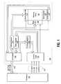
- FIG. 1is a simplified block diagram of a NAND flash memory device 100 coupled to a processor 130 as part of an electronic system, according to an embodiment of the invention.
- electronic systemsinclude personal computers, personal digital assistants (PDAs), digital cameras, digital media players, digital recorders, games, appliances, vehicles, wireless devices, cellular telephones and the like.
- the processor 130may be a memory controller or other external processor.
- Memory device 100includes an array of memory cells 104 arranged in rows and columns and having an architecture in accordance with an embodiment of the invention.
- a row decoder 108 and a column decoder 110are provided to decode address signals. Address signals are received and decoded to access memory array 104 .
- Memory device 100also includes input/output (I/O) control circuitry 112 to manage input of commands, addresses and data to the memory device 100 as well as output of data and status information from the memory device 100 .
- I/O control circuitry 112to manage input of commands, addresses and data to the memory device 100 as well as output of data and status information from the memory device 100 .
- An address register 114is coupled between I/O control circuitry 112 and row decoder 108 and column decoder 110 to latch the address signals prior to decoding.
- a command register 124is coupled between I/O control circuitry 112 and control logic 116 to latch incoming commands.
- Control logic 116controls access to the memory array 104 in response to the commands and generates status information for the external processor 130 .
- the control logic 116is coupled to row decoder 108 and column decoder 110 to control the row decoder 108 and column decoder 110 in response to the addresses.
- Control logic 116is also coupled to a cache register 118 .
- Cache register 118latches data, either incoming or outgoing, as directed by control logic 116 to temporarily store data while the memory array 104 is busy writing or reading, respectively, other data.
- datais passed from the cache register 118 to data register 120 for transfer to the memory array 104 ; then new data is latched in the cache register 118 from the I/O control circuitry 112 .
- During a read operationdata is passed from the cache register 118 to the I/O control circuitry 112 for output to the external processor 130 ; then new data is passed from the data register 120 to the cache register 118 .
- a status register 122is coupled between I/O control circuitry 112 and control logic 116 to latch the status information for output to the processor 130 .
- Memory device 100receives control signals at control logic 116 from processor 130 over a control link 132 .
- the control signalsmay include a chip enable CE#, a command latch enable CLE, an address latch enable ALE, and a write enable WE# in accordance with the present invention.
- Memory device 100receives command signals (or commands), address signals (or addresses), and data signals (or data) from processor 130 over a multiplexed input/output (I/O) bus 134 and outputs data to processor 130 over I/O bus 134 .
- I/Oinput/output
- the commandsare received over input/output (I/O) pins [ 0 : 7 ] of I/O bus 134 at I/O control circuitry 112 and are written into command register 124 .
- the addressesare received over input/output (I/O) pins [ 0 : 7 ] of bus 134 at I/O control circuitry 112 and are written into address register 114 .
- the dataare received over input/output (I/O) pins [ 0 : 7 ] for an 8-bit device or input/output (I/O) pins [ 0 : 15 ] for a 16-bit device at I/O control circuitry 112 and are written into cache register 118 .
- the dataare subsequently written into data register 120 for programming memory array 104 .
- cache register 118may be omitted, and the data are written directly into data register 120 .
- Dataare also output over input/output (I/O) pins [ 0 : 7 ] for an 8-bit device or input/output (I/O) pins [ 0 : 15 ] for a 16-bit device.
- I/Oinput/output
- additional circuitry and control signalscan be provided, and that the memory device of FIG. 1 has been simplified to help focus on the invention.
- specific I/O pinsare described in accordance with popular conventions for receipt and output of the various signals, it is noted that other combinations or numbers of I/O pins may be used in the various embodiments.
- FIG. 2is a schematic of a portion of an example NAND memory array 200 of the prior art included for comparison.
- the memory array 200includes word lines 202 1 to 202 N and intersecting bit lines 204 1 to 204 M .
- the number of word lines 202 and the number of bit lines 204are generally each some power of two.
- Memory array 200includes NAND strings 206 1 to 206 M .
- Each NAND stringincludes transistors 208 1 to 208 N , each located at an intersection of a word line 202 and a bit line 204 .
- the transistors 208depicted as floating-gate transistors in FIG. 2 , represent non-volatile memory cells for storage of data.
- the floating-gate transistors 208 of each NAND string 206are connected in series source to drain between a source select gate 210 , e.g., a field-effect transistor (FET), and a drain select gate 212 , e.g., a FET.
- Each source select gate 210is located at an intersection of a bit line 204 and a source select line 214
- each drain select gate 212is located at an intersection of a bit line 204 and a drain select line 215 .
- a source of each source select gate 210is connected to a common source line 216 .
- the drain of each source select gate 210is connected to the source of the first floating-gate transistor 208 of the corresponding NAND string 206 .
- the drain of source select gate 210 1is connected to the source of floating-gate transistor 208 1 of the corresponding NAND string 206 1 .
- each drain select gate 212is connected to a bit line 204 for the corresponding NAND string.
- the drain of drain select gate 212 1is connected to the bit line 204 1 for the corresponding NAND string 206 1 .
- the source of each drain select gate 212is connected to the drain of the last floating-gate transistor 208 of the corresponding NAND string 206 .
- the source of drain select gate 212 1is connected to the drain of floating-gate transistor 208 N of the corresponding NAND string 206 1 .
- Typical construction of floating-gate transistors 208includes a source 230 and a drain 232 , a floating gate 234 , and a control gate 236 , as shown in FIG. 2 .
- Floating-gate transistors 208have their control gates 236 coupled to a word line 202 .
- a column of the floating-gate transistors 208are those NAND strings 206 coupled to a given bit line 204 .
- a row of the floating-gate transistors 208are those transistors commonly coupled to a given word line 202 .
- unselected word lines of a block of memory cellsare typically operated as pass gates while a selected word line receives a different control potential to allow its data state to determine the conductance of its associated strings of memory cells.
- a word line associated with a selected row of memory cellsis driven at a selected read level voltage Vread, which is typically a low voltage (such as 0V or ground).
- Vreadtypically a low voltage (such as 0V or ground).
- Vpasssuch as 4.5V
- FIG. 3Ais a schematic of a portion of a NAND memory array 300 A in accordance with an embodiment of the invention.
- the memory array 300 Aincludes word lines 302 0 to 302 N and intersecting bit lines 304 0 to 304 M using a layout similar to that of NAND memory array 200 .
- the number of word lines 302 and the number of bit lines 304are generally each some power of two.
- Memory array 300 Aincludes NAND strings 306 0 and 306 1 . It is noted that typical memory arrays may contain millions of such strings 306 selectively coupled to bit lines 304 in a many to one relationship.
- Each NAND string 306includes field-effect transistors 308 0 to 308 N , each located at an intersection of a word line 302 and a bit line 304 .
- the transistors 308depicted as floating-gate transistors in FIG. 3A , represent non-volatile memory cells for storage of data.
- the memory array 300 Ais depicted as an array of floating-gate transistors, other non-volatile memory technologies capable of defining a data value by a change in threshold voltage may also be used, such as NROM, floating-node, ferroelectric, magnetic and the like. Each data value typically corresponds to mutually exclusive ranges of threshold voltages.
- the floating-gate transistors 308 of each NAND string 306are connected in series, sharing source/drain regions with adjacent memory cells, between a first select gate 312 , e.g., a FET, and a second select gate 313 , e.g., a FET.
- Each first select gate 312is located at an intersection of a bit line 304 and first select lines 315 1-1 / 315 1-2
- each second select gate 313is located at an intersection of a bit line 304 and a second select line 315 2 .
- the NAND memory array 300 Ain accordance with an embodiment of the invention has no select gate coupled to a source line.
- the NAND memory array 300 Ahas both select gates 312 and 313 of a NAND string 306 coupled to a bit line 304 .
- the NAND strings 306are coupled to use a bit line 304 as a charge storage node for charge sharing during a read operation. For example, presume that NAND string 306 1 is sensed using bit line 304 1 . That is, bit line 304 1 is selectively coupled to a sensing device 320 , such as by a multiplexer 317 , when determining a data value of a target memory cell 308 in NAND string 306 1 . The multiplexer 317 selectively couples one bit line 304 to sensing device 320 while decoupling remaining bit lines 304 .
- bit lines 304are depicted coupled to multiplexer 317 , additional levels of multiplexing may be used such that a sensing device 320 could be selectively coupled to one of many bit lines 304 .
- NAND string 306 1will then use a second bit line, such as adjacent bit line 304 0 , as a charge storage node.
- adjacent bit line 304 0is sensed using bit line 304 0 , it could use adjacent bit line 304 1 as its charge storage node.
- the NAND memory array 300 Ais depicted with a pair of NAND strings 306 0 / 306 1 sharing the same pair of bit lines 304 0 / 304 1 , such is not a requirement.
- NAND string 306 1could use a bit line to its right, i.e., bit line 304 2 , in a manner similar to the coupling of NAND string 306 0 to bit line 304 1 .
- the bit line used as a charge storage nodeneed only be decoupled from its sensing device when being used as a charge storage node for the bit line being sensed.
- a first source/drain region of each first select gate 312is connected to a bit line 304 .
- a second source/drain region of each first select gate 312is connected to a first source/drain region of the first floating-gate transistor 308 of the corresponding NAND string 306 .
- the first source/drain region of the first select gate 312 0is connected to bit line 304 1 and the second source/drain region of the first select gate 312 0 is connected to the first source/drain region of floating-gate transistor 308 0 of the corresponding NAND string 306 0 .
- a second source/drain region of each second select gate 313is connected to a different bit line 304 than its corresponding first source select gate 312 while a first source/drain region of each select gate 313 is connected to a second source/drain region of the last floating-gate transistor 308 of the corresponding NAND string 306 .
- the first source/drain region of source select gate 313 0is connected to second source/drain region of floating-gate transistor 308 N of the corresponding NAND string 306 0 and the second source/drain region of the source select gate 313 0 is connected to the bit line 304 0 .
- FIG. 3Adepicts just one example of how this can be accomplished.
- the first select gate 312 0 associated with NAND string 306 0may receive a first control signal via first select line 315 1-1 while first select gate 312 1 associated with NAND string 306 1 may receive a second control signal via first select line 315 1-2 .
- NAND string 306 0could be coupled to bit line 304 1 while NAND string 306 1 is decoupled from bit line 304 0 or vice versa.
- similar treatmentcould be applied to the second select gates 313 to selectively decouple one NAND string 306 from both bit lines 304 0 and 304 1 while the other NAND string 306 is coupled to both.
- FIG. 3Bis a schematic of a portion of a NAND memory array 300 B in accordance with an embodiment of the invention.
- the memory array 300 Bhas the substantially same basic layout as memory array 300 A of FIG. 3A , but uses a different technique to selectively decouple one NAND string 306 from both bit lines 304 0 and 304 1 while the other NAND string 306 is coupled to both.
- two rows of first select gates 312are used, with each row of select gates 312 receiving the same control signal through a first select line 315 1 .
- first select gates 312 of each rowalternate between enhancement mode devices, i.e., in a normally deactivated state, and depletion mode devices, i.e., in a normally activated state.
- the differing device modesmay be created by modifying doping levels in alternating devices.
- first select gate 312 0-1may be an enhancement mode device while the first select gate 312 1-1 is a depletion mode device.
- a supply potential Vcc applied to select line 315 1-1would activate both first select gates 312 0-1 and 312 1-1 while a ground potential Vss applied to select line 315 1-1 would deactivate first select gate 312 0-1 and activate first select gate 312 1-1 .
- first select gate 312 0-2would be a depletion mode device while first select gate 312 1-2 would be an enhancement mode device.
- even select gates of a first row of select gates 312 and odd select gates of a second row of select gates 312would be enhancement mode devices while odd select gates of the first row of select gates 312 and even select gates of the second row of select gates 312 would be depletion mode devices.
- a supply potential Vcc applied to select line 315 1-2would activate both first select gates 312 0-2 and 312 1-2 while a ground potential Vss applied to select line 315 1-2 would deactivate first select gate 312 0-2 and activate first select gate 312 1-2 .
- applying the supply potential Vcc to the select line 315 1-1 and the ground potential Vss to select line 315 1-2would couple NAND string 306 0 to bit line 304 1 and isolate NAND string 306 1 from bit line 304 0 .
- first select gates 312act in a coordinated manner, a pair of enhancement mode and depletion mode devices associated with a single NAND string 306 , e.g., first select gates 312 0-1 and 312 0-2 , may be referred to collectively as a first select gate 312 , e.g., first select gate 312 0 , for purposes of this disclosure.
- first select gate 312e.g., first select gate 312 0
- the same treatmentcould be applied to the other end of the NAND strings 306 to achieve additional levels of isolation.
- each NAND string 306It may be desirable or necessary to provide for isolation at both ends of each NAND string 306 from the bit lines 304 .
- Vssground potential
- select line 315 1-1 and 315 1-2or applying a negative control voltage to either select line 315 1-1 or 315 1-2 , at least one first select gate 312 would be deactivated for each NAND string 306 . While various examples were described to facilitate use of bit lines 304 as charge storage nodes, other methods could be used to produce the same or substantially similar results.
- a column of the transistors or memory cells 308are those NAND strings 306 coupled to a given bit line 304 .
- a row of the transistors or memory cells 308are those transistors commonly coupled to a given word line 302 .
- Other forms of transistors 308may also be utilized with embodiments of the invention, such as NROM, magnetic or ferroelectric transistors and other transistors capable of being programmed to assume one of two or more threshold voltages indicative of data states.
- memory arrays in accordance with embodiments of the inventioncan be fabricated using less die area and fewer processing steps, thus facilitating increased yield and higher memory densities.
- traditional NAND memory arrays 200rely on conductance of its NAND strings 206 for read operations, larger string lengths are discouraged due to the increases in resistance which tend to increase read times and make it more difficult to distinguish between different data values.
- string lengthhas only nominal impact on the read performance.
- Programming and erasing memory cells 308 of the NAND arrays 300can be performed similar to programming and erasing memory cells 208 of the prior-art NAND array 200 .
- the word line 302 1 containing the target memory cell 308 1may receive a programming voltage that is some positive potential capable of programming a memory cell in conjunction with the remaining node voltages.
- the programming voltagemay be about 20V.
- Unselected word lines 302i.e., word lines 302 0 and 302 2 - 302 N not associated with the target memory cell 308 1 , receive some positive potential capable of causing memory cells on the unselected word lines to act as pass gates during the programming of the selected word line.
- the pass voltage during programmingmay be about 10V.
- the selected bit line 304i.e., the bit line 304 0 associated with the target memory cell 308 1 , might receive the ground potential Vss while unselected bit lines 304 , e.g., bit lines 304 1 - 304 M not associated with the target memory cell 308 1 , might receive a higher potential, such as the supply potential Vcc. Note that while this example describes programming only one target memory cell 308 , there may be more than one selected bit line 304 as more than one target memory cell 308 on a given word line 302 can be programmed concurrently.
- One set of select gatessuch as first select gates 312 or isolation gates 314 , if used, might receive the same potential as the selected bit lines 304 , such as ground potential Vss, on their gates.
- An opposing set of select gates, such as second select gates 313might receive some positive potential, such as the supply potential Vcc, on their gates sufficient to activate those select gates coupled to selected bit lines.
- the bulk substrate in which the memory cells 308 are formedmight be held at the ground potential Vss.
- Erasing of memory cells 308would generally be performed concurrently to a block of memory cells.
- all word lines 302might receive the ground potential Vss
- all bit lines 304may be electrically floating
- the select linesmay be electrically floating while the bulk substrate in which the memory cells 308 are formed is boosted to some erase voltage, such as 20V.
- the foregoingrepresents just one set of techniques for programming and erasing memory cells of a NAND memory array 300 of the type depicted in FIGS. 3A and 3B . It is noted that because typical programming and erase operations do not make use of the source connection of a traditional NAND memory array, many techniques for programming and erasing a traditional NAND memory array 200 can also be applied to NAND memory arrays 300 A/ 300 B in accordance with embodiments of the invention. However, because the NAND strings 306 in accordance with embodiments of the invention eliminate the need for a source connection, typical read operations relying on conductance of a string of memory cells are unsuitable for use with embodiments of the invention.
- various embodiments of the inventionrely on capacitance of a bit line during a read operation.
- a chargeis placed on a bit line not containing the target memory cell and then selectively released or increased depending upon the data value stored in the target memory cell.
- the target memory cell or cellsare then read using charge sharing techniques to raise or lower a voltage on their associated bit lines. If the charge on the bit line not containing the target memory cell is greater than the bit line associated with the target memory cell, the associated bit line receives the charge and increases its voltage level. If the charge is less, the associated bit line loses charge to the storage node bit line and decreases its voltage level.
- the time expected for precharging the strings of memory cells, selectively releasing or increasing the charge and reading the data value using charge sharing techniquesis expected to be on the order of several hundred nanoseconds versus several microseconds used for traditional conductance read operations.
- FIG. 4is a flow chart of a method of reading memory cells in accordance with an embodiment of the invention.
- a first bit linei.e., the bit line being used as a storage node
- a read operationwould read memory cells 308 coupled to a selected word line 302 across a number of bit lines 304 .
- a read operationmay be performed on every other bit line of a block of memory cells.
- the remaining bit linescould be used as storage nodes and thus each could be precharged using the first predetermined voltage.
- the target memory cellis in NAND string 306 0
- the bit line 304 1could be precharged using the first predetermined voltage.
- the bit line 304 1could be driven to the first predetermined voltage, such as the supply potential Vcc or the ground potential Vss, while the bit line 304 1 is isolated from the NAND strings 306 0 and 306 1 . After precharging, the bit line 304 1 would be isolated, thus retaining its charge. Note that the stored charge may be a positive, negative or neutral charge depending upon the chosen voltage.
- charge stored on the first bit linesis selectively removed or added based on the data values of the target memory cells.
- the NAND string 306 containing the target memoryis made conductive if the target memory cell has a first data value and non-conductive if it has a second data value and the first select gate 312 between the bit line 304 and the NAND string 306 is activated.
- Chargecan then be selectively removed or added through the NAND string 306 depending upon the data value of the target memory cell.
- the following exampledescribes how charge can be selectively removed where the bit line acting as a charge storage node has been precharged using a positive voltage, such as Vcc.
- the selected word line 302 1 coupled to the target memory cell 308 1may receive a potential to activate the memory cell if it has a first data value, e.g., “1” or erased, and to deactivate the memory cell if it has a second data value, e.g., “0” or programmed.
- a first data valuee.g., “1” or erased
- a second data valuee.g., “0” or programmed.
- an erased memory cellgenerally has a threshold voltage of less than 0V while a programmed memory cell might have a threshold voltage of around 1V or higher.
- Remaining word lines 302would receive a potential to activate their memory cells regardless of their data values, and first select gate 312 0 and second select gate 313 0 would receive a potential to activate these select gates.
- the bit line 304 0By dropping the bit line 304 0 to the ground potential Vss, while the select gate 313 0 is activated, the select gate 312 0 is activated and the unselected word lines are acting as pass gates, the bit line 304 1 would lose its charge to the bit line 304 0 if the memory cell 308 1 were activated. However, if the memory cell 308 1 were deactivated, charge would be retained in the bit line 304 1 .
- a similar processcould be used in this example to selectively add charge to the charge storage node.
- the bit line 304 1could be precharged using the ground potential Vss.
- Vssground potential
- chargewould be added to the bit line 304 1 if the target memory cell 308 1 were activated and charge would be retained if the memory cell 3081 were deactivated.
- the second bit lines 304 to be read or sensedare precharged to a second predetermined voltage.
- the prechargingmay occur with the NAND strings 306 isolated from the second bit lines 304 , such as by deactivating both select gates 312 and 313 .
- the prechargingmay occur with the NAND strings 306 coupled to the second bit lines 304 being sensed provided that the bit lines 304 acting as storage nodes are isolated from the NAND strings 306 .
- the second predetermined voltageis an intermediate value between the first predetermined voltage and the bit line voltage used when selectively removing or adding charge from the first bit lines acting as storage nodes. In this manner, if a stored charge is retained, charge sharing will tend to drive the bit line being sensed in one direction from the second predetermined voltage, and if the stored charge is removed or added, charge sharing will tend to drive the bit line being sensed in an opposite direction from the second predetermined voltage. For example, if the bit line 304 1 was charged to the supply potential Vcc, and the resulting stored charge were retained, sharing the stored charge from the bit line 304 1 would tend to increase the potential of a bit line 304 0 if it were precharged to a second predetermined voltage of less than Vcc.
- the second predetermined voltagewould then be chosen to be some value greater than approximately Vss and less than approximately Vcc.
- a second predetermined voltage of approximately Vcc/2might be used in this scenario.
- the second predetermined voltagemay further have a value equal to the bit line voltage used when selectively removing charge from the NAND strings.
- the second predetermined voltagemay further have a value equal to the first predetermined voltage.
- the data value of the memory cellwould be indicated by no change in the second bit line voltage upon equalization with the first bit line.
- charge sharingoccurs between the first bit lines and the second bit lines by equalizing the two.
- charge sharingmight be accomplished by driving all word lines 302 to the pass voltage Vpass to act as pass gates while activating both of the select gates 312 and 313 .
- the data values of the target memory cells 308are determined based on the resulting voltage changes of their associated bit lines 304 . Sensing of data values in this manner is well understood and is commonly utilized in DRAM devices. As one example, a differential sensing technique could be utilized. In this technique, during the precharging of the bit line at 444 , a reference bit line could also be precharged and equalized to the bit line being sensed. The reference bit line would be isolated from the second bit line being sensed before performing the charge sharing at 446 .
- a single-ended sensing devicehas a single input coupled to a target bit line and often contains an inverter providing an output signal indicative of the potential level of the target bit line and, thus, the data value of the target memory cell.
- the inverterwould generally have a threshold point close to the precharge potential.
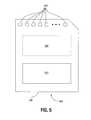
- FIG. 5is an illustration of an exemplary memory module 500 .
- Memory module 500is illustrated as a memory card, although the concepts discussed with reference to memory module 500 are applicable to other types of removable or portable memory, e.g., USB flash drives, and are intended to be within the scope of “memory module” as used herein.
- memory modulee.g., USB flash drives
- FIG. 5shows one example form factor, these concepts are applicable to other form factors as well.
- memory module 500will include a housing 505 (as depicted) to enclose one or more memory devices 510 , though such a housing is not essential to all devices or device applications.
- At least one memory device 510is a non-volatile memory having a NAND architecture in accordance with an embodiment of the invention.
- the housing 505includes one or more contacts 515 for communication with a host device. Examples of host devices include digital cameras, digital recording and playback devices, PDAs, personal computers, memory card readers, interface hubs and the like.
- the contacts 515are in the form of a standardized interface. For example, with a USB flash drive, the contacts 515 might be in the form of a USB Type-A male connector.
- the contacts 515are in the form of a semi-proprietary interface, such as might be found on CompactFlashTM memory cards licensed by SanDisk Corporation, Memory StickTM memory cards licensed by Sony Corporation, SD Secure DigitalTM memory cards licensed by Toshiba Corporation and the like. In general, however, contacts 515 provide an interface for passing control, address and/or data signals between the memory module 500 and a host having compatible receptors for the contacts 515 .
- the memory module 500may optionally include additional circuitry 520 which may be one or more integrated circuits and/or discrete components.
- the additional circuitry 520may include a memory controller for controlling access across multiple memory devices 510 and/or for providing a translation layer between an external host and a memory device 510 .
- a memory controllercould selectively couple an I/O connection (not shown in FIG. 5 ) of a memory device 510 to receive the appropriate signal at the appropriate I/O connection at the appropriate time or to provide the appropriate signal at the appropriate contact 515 at the appropriate time.
- the communication protocol between a host and the memory module 500may be different than what is required for access of a memory device 510 .
- a memory controllercould then translate the command sequences received from a host into the appropriate command sequences to achieve the desired access to the memory device 510 .
- Such translationmay further include changes in signal voltage levels in addition to command sequences.
- the additional circuitry 520may further include functionality unrelated to control of a memory device 510 such as logic functions as might be performed by an ASIC (application specific integrated circuit). Also, the additional circuitry 520 may include circuitry to restrict read or write access to the memory module 500 , such as password protection, biometrics or the like. The additional circuitry 520 may include circuitry to indicate a status of the memory module 500 . For example, the additional circuitry 520 may include functionality to determine whether power is being supplied to the memory module 500 and whether the memory module 500 is currently being accessed, and to display an indication of its status, such as a solid light while powered and a flashing light while being accessed. The additional circuitry 520 may further include passive devices, such as decoupling capacitors to help regulate power requirements within the memory module 500 .
- NAND memory array architectureshaving series-coupled strings of non-volatile memory cells where ends of the string are selectively coupled to different bit lines, and methods of reading a NAND memory array using charge sharing techniques, have been described. Such methods and apparatus facilitate increased memory densities, reduced fabrication steps and faster read operations when compared to traditional NAND memory array architectures.
Landscapes
- Engineering & Computer Science (AREA)
- Microelectronics & Electronic Packaging (AREA)
- Read Only Memory (AREA)
- Semiconductor Memories (AREA)
- Non-Volatile Memory (AREA)
Abstract
Description
- The present invention relates generally to semiconductor memory devices, and in particular, the present invention relates to NAND architecture memory devices and their operation and use.
- Memory devices are typically provided as internal, semiconductor, integrated circuits in computers or other electronic devices. There are many different types of memory including random-access memory (RAM), read only memory (ROM), dynamic random access memory (DRAM), synchronous dynamic random access memory (SDRAM), and flash memory.
- Flash memory devices have developed into a popular source of non-volatile memory for a wide range of electronic applications. Flash memory devices typically use a one-transistor memory cell that allows for high memory densities, high reliability, and low power consumption. Changes in threshold voltage of the cells, through programming of charge storage or trapping layers or other physical phenomena, determine the data value of each cell. Common uses for flash memory include personal computers, personal digital assistants (PDAs), digital cameras, digital media players, digital recorders, games, appliances, vehicles, wireless devices, cellular telephones, and removable memory modules, and the uses for flash memory continue to expand.
- Flash memory typically utilizes one of two basic architectures known as NOR flash and NAND flash. The designation is derived from the logic used to read the devices. In NOR flash architecture, a column of memory cells are coupled in parallel with each memory cell coupled to a bit line. In NAND flash architecture, a column of memory cells are coupled in series with only the first memory cell of the column coupled to a bit line.
- As the performance of electronic systems employing flash memory devices increases, flash memory device performance should also increase. A performance increase includes reducing power consumption, increasing speed, and increasing the memory density.
- For the reasons stated above, and for other reasons stated below which will become apparent to those skilled in the art upon reading and understanding the present specification, there is a need in the art for alternative NAND memory architectures and their operation.
FIG. 1 is a functional block diagram of an electronic system having at least one memory device in accordance with an embodiment of the invention.FIG. 2 is a schematic of a portion of an example NAND memory array of the prior art.FIG. 3A is a schematic of a portion of a NAND memory array in accordance with an embodiment of the invention.FIG. 3B is a schematic of a portion of a NAND memory array in accordance with another embodiment of the invention.FIG. 4 is a flow chart of a method of reading memory cells in accordance with an embodiment of the invention.FIG. 5 is a functional block diagram of a memory module having at least one memory device in accordance with an embodiment of the invention.- In the following detailed description of the present embodiments, reference is made to the accompanying drawings that form a part hereof, and in which is shown by way of illustration specific embodiments in which the inventions may be practiced. These embodiments are described in sufficient detail to enable those skilled in the art to practice the invention, and it is to be understood that other embodiments may be utilized and that process, electrical or mechanical changes may be made without departing from the scope of the present invention. The following detailed description is, therefore, not to be taken in a limiting sense, and the scope of the present invention is defined only by the appended claims and equivalents thereof.
- Non-volatile memory devices are described utilizing a modified NAND architecture where ends of the NAND string of memory cells are selectively coupled to different bit lines. Programming and erasing of the memory cells can be accomplished in the same manner as a traditional NAND memory array. However, reading of the memory cells in accordance with embodiments of the invention is accomplished using charge sharing techniques similar to read operations in a DRAM device.
- The NAND architectures of the various embodiments include strings of two or more series-coupled field-effect transistor non-volatile memory cells whose data values are determined by their threshold voltages. A first of the series-coupled memory cells of a string is selectively coupled to a first bit line through a first select gate. A last of the series-coupled memory cells of the string is selectively coupled to a second bit line through a second select gate. During a read operation of a target memory cell of string, the second or adjacent bit line serves as a storage node for a charge that is indicative of the data value of the target memory cell.
FIG. 1 is a simplified block diagram of a NANDflash memory device 100 coupled to aprocessor 130 as part of an electronic system, according to an embodiment of the invention. Some examples of electronic systems include personal computers, personal digital assistants (PDAs), digital cameras, digital media players, digital recorders, games, appliances, vehicles, wireless devices, cellular telephones and the like. Theprocessor 130 may be a memory controller or other external processor.Memory device 100 includes an array ofmemory cells 104 arranged in rows and columns and having an architecture in accordance with an embodiment of the invention. Arow decoder 108 and acolumn decoder 110 are provided to decode address signals. Address signals are received and decoded to accessmemory array 104.Memory device 100 also includes input/output (I/O)control circuitry 112 to manage input of commands, addresses and data to thememory device 100 as well as output of data and status information from thememory device 100. Anaddress register 114 is coupled between I/O control circuitry 112 androw decoder 108 andcolumn decoder 110 to latch the address signals prior to decoding. Acommand register 124 is coupled between I/O control circuitry 112 andcontrol logic 116 to latch incoming commands.Control logic 116 controls access to thememory array 104 in response to the commands and generates status information for theexternal processor 130. Thecontrol logic 116 is coupled torow decoder 108 andcolumn decoder 110 to control therow decoder 108 andcolumn decoder 110 in response to the addresses.Control logic 116 is also coupled to acache register 118. Cache register118 latches data, either incoming or outgoing, as directed bycontrol logic 116 to temporarily store data while thememory array 104 is busy writing or reading, respectively, other data. During a write operation, data is passed from thecache register 118 todata register 120 for transfer to thememory array 104; then new data is latched in thecache register 118 from the I/O control circuitry 112. During a read operation, data is passed from thecache register 118 to the I/O control circuitry 112 for output to theexternal processor 130; then new data is passed from thedata register 120 to thecache register 118. A status register122 is coupled between I/O control circuitry 112 andcontrol logic 116 to latch the status information for output to theprocessor 130.Memory device 100 receives control signals atcontrol logic 116 fromprocessor 130 over acontrol link 132. The control signals may include a chip enable CE#, a command latch enable CLE, an address latch enable ALE, and a write enable WE# in accordance with the present invention.Memory device 100 receives command signals (or commands), address signals (or addresses), and data signals (or data) fromprocessor 130 over a multiplexed input/output (I/O)bus 134 and outputs data toprocessor 130 over I/O bus 134.- Specifically, the commands are received over input/output (I/O) pins [0:7] of I/
O bus 134 at I/O control circuitry 112 and are written intocommand register 124. The addresses are received over input/output (I/O) pins [0:7] ofbus 134 at I/O control circuitry 112 and are written intoaddress register 114. The data are received over input/output (I/O) pins [0:7] for an 8-bit device or input/output (I/O) pins [0:15] for a 16-bit device at I/O control circuitry 112 and are written intocache register 118. The data are subsequently written intodata register 120 forprogramming memory array 104. For another embodiment,cache register 118 may be omitted, and the data are written directly intodata register 120. Data are also output over input/output (I/O) pins [0:7] for an 8-bit device or input/output (I/O) pins [0:15] for a 16-bit device. It will be appreciated by those skilled in the art that additional circuitry and control signals can be provided, and that the memory device ofFIG. 1 has been simplified to help focus on the invention. Additionally, while specific I/O pins are described in accordance with popular conventions for receipt and output of the various signals, it is noted that other combinations or numbers of I/O pins may be used in the various embodiments. FIG. 2 is a schematic of a portion of an exampleNAND memory array 200 of the prior art included for comparison. As shown inFIG. 2 , thememory array 200 includes word lines2021to202Nand intersecting bit lines2041to204M. For ease of addressing in the digital environment, the number of word lines202 and the number of bit lines204 are generally each some power of two.Memory array 200 includes NAND strings2061to206M. Each NAND string includes transistors2081to208N, each located at an intersection of a word line202 and a bit line204. The transistors208, depicted as floating-gate transistors inFIG. 2 , represent non-volatile memory cells for storage of data. The floating-gate transistors208 of each NAND string206 are connected in series source to drain between a source select gate210, e.g., a field-effect transistor (FET), and a drain select gate212, e.g., a FET. Each source select gate210 is located at an intersection of a bit line204 and a sourceselect line 214, while each drain select gate212 is located at an intersection of a bit line204 and a drainselect line 215.- A source of each source select gate210 is connected to a
common source line 216. The drain of each source select gate210 is connected to the source of the first floating-gate transistor208 of the corresponding NAND string206. For example, the drain of source select gate2101is connected to the source of floating-gate transistor2081of the corresponding NAND string2061. - The drain of each drain select gate212 is connected to a bit line204 for the corresponding NAND string. For example, the drain of drain select gate2121is connected to the bit line2041for the corresponding NAND string2061. The source of each drain select gate212 is connected to the drain of the last floating-gate transistor208 of the corresponding NAND string206. For example, the source of drain select gate2121is connected to the drain of floating-gate transistor208Nof the corresponding NAND string2061.
- Typical construction of floating-gate transistors208 includes a
source 230 and adrain 232, a floatinggate 234, and acontrol gate 236, as shown inFIG. 2 . Floating-gate transistors208 have theircontrol gates 236 coupled to a word line202. A column of the floating-gate transistors208 are those NAND strings206 coupled to a given bit line204. A row of the floating-gate transistors208 are those transistors commonly coupled to a given word line202. - To read memory cells in the prior art NAND architecture memory array of
FIG. 2 , unselected word lines of a block of memory cells are typically operated as pass gates while a selected word line receives a different control potential to allow its data state to determine the conductance of its associated strings of memory cells. In general, a word line associated with a selected row of memory cells is driven at a selected read level voltage Vread, which is typically a low voltage (such as 0V or ground). In addition, the word lines connected to the gates the unselected memory cells of each string are driven by a pass voltage Vpass (such as 4.5V) to operate the unselected memory cells of each string as pass gates. This allows them to pass current in a manner that is unrestricted by their stored data values. In a read operation, current then flows from the source line to the column bit line through each series-connected string, restricted only by the memory cell selected to be read in each string. The data value of a selected memory cell of a string is then determined by sensing a level of current flow through its associated string. FIG. 3A is a schematic of a portion of aNAND memory array 300A in accordance with an embodiment of the invention. As shown inFIG. 3A , thememory array 300A includesword lines 3020to302Nand intersecting bit lines3040to304Musing a layout similar to that ofNAND memory array 200. For ease of addressing in the digital environment, the number ofword lines 302 and the number of bit lines304 are generally each some power of two.Memory array 300A includes NAND strings3060and3061. It is noted that typical memory arrays may contain millions of such strings306 selectively coupled to bit lines304 in a many to one relationship. Each NAND string306 includes field-effect transistors3080to308N, each located at an intersection of aword line 302 and a bit line304. The transistors308, depicted as floating-gate transistors inFIG. 3A , represent non-volatile memory cells for storage of data. Although thememory array 300A is depicted as an array of floating-gate transistors, other non-volatile memory technologies capable of defining a data value by a change in threshold voltage may also be used, such as NROM, floating-node, ferroelectric, magnetic and the like. Each data value typically corresponds to mutually exclusive ranges of threshold voltages. The floating-gate transistors308 of each NAND string306 are connected in series, sharing source/drain regions with adjacent memory cells, between a first select gate312, e.g., a FET, and a second select gate313, e.g., a FET. Each first select gate312 is located at an intersection of a bit line304 and first select lines3151-1/3151-2, while each second select gate313 is located at an intersection of a bit line304 and a second select line3152. Unlike the traditionalNAND memory array 200 ofFIG. 2 , theNAND memory array 300A in accordance with an embodiment of the invention has no select gate coupled to a source line. In contrast, theNAND memory array 300A has both select gates312 and313 of a NAND string306 coupled to a bit line304.- The NAND strings306 are coupled to use a bit line304 as a charge storage node for charge sharing during a read operation. For example, presume that NAND string3061is sensed using bit line3041. That is, bit line3041is selectively coupled to a
sensing device 320, such as by amultiplexer 317, when determining a data value of a target memory cell308 in NAND string3061. Themultiplexer 317 selectively couples one bit line304 tosensing device 320 while decoupling remaining bit lines304. Although only two bit lines304 are depicted coupled tomultiplexer 317, additional levels of multiplexing may be used such that asensing device 320 could be selectively coupled to one of many bit lines304. NAND string3061will then use a second bit line, such as adjacent bit line3040, as a charge storage node. Similarly, if NAND string3060is sensed using bit line3040, it could use adjacent bit line3041as its charge storage node. While theNAND memory array 300A is depicted with a pair of NAND strings3060/3061sharing the same pair of bit lines3040/3041, such is not a requirement. For example, NAND string3061could use a bit line to its right, i.e., bit line3042, in a manner similar to the coupling of NAND string3060to bit line3041. The bit line used as a charge storage node need only be decoupled from its sensing device when being used as a charge storage node for the bit line being sensed. - A first source/drain region of each first select gate312 is connected to a bit line304. A second source/drain region of each first select gate312 is connected to a first source/drain region of the first floating-gate transistor308 of the corresponding NAND string306. For example, the first source/drain region of the first select gate3120is connected to bit line3041and the second source/drain region of the first select gate3120is connected to the first source/drain region of floating-gate transistor3080of the corresponding NAND string3060. At the opposing end of the string, a second source/drain region of each second select gate313 is connected to a different bit line304 than its corresponding first source select gate312 while a first source/drain region of each select gate313 is connected to a second source/drain region of the last floating-gate transistor308 of the corresponding NAND string306. For example, the first source/drain region of source select gate3130is connected to second source/drain region of floating-gate transistor308Nof the corresponding NAND string3060and the second source/drain region of the source select gate3130is connected to the bit line3040.
- In order to utilize a bit line304 as a charge storage node, it must be isolated from the bit line being sensed except through the NAND string306 containing the target memory cell308.
FIG. 3A depicts just one example of how this can be accomplished. For example, the first select gate3120associated with NAND string3060may receive a first control signal via first select line3151-1while first select gate3121associated with NAND string3061may receive a second control signal via first select line3151-2. By applying complementary signals to the first select lines3151-1and3151-1, NAND string3060could be coupled to bit line3041while NAND string3061is decoupled from bit line3040or vice versa. For increased isolation, similar treatment could be applied to the second select gates313 to selectively decouple one NAND string306 from both bit lines3040and3041while the other NAND string306 is coupled to both. FIG. 3B is a schematic of a portion of aNAND memory array 300B in accordance with an embodiment of the invention. Thememory array 300B has the substantially same basic layout asmemory array 300A ofFIG. 3A , but uses a different technique to selectively decouple one NAND string306 from both bit lines3040and3041while the other NAND string306 is coupled to both. For the embodiment ofFIG. 3B , two rows of first select gates312 are used, with each row of select gates312 receiving the same control signal through a first select line3151. However, the first select gates312 of each row alternate between enhancement mode devices, i.e., in a normally deactivated state, and depletion mode devices, i.e., in a normally activated state. The differing device modes may be created by modifying doping levels in alternating devices. For example, as depicted inFIG. 3B , first select gate3120-1may be an enhancement mode device while the first select gate3121-1is a depletion mode device. Thus, a supply potential Vcc applied to select line3151-1would activate both first select gates3120-1and3121-1while a ground potential Vss applied to select line3151-1would deactivate first select gate3120-1and activate first select gate3121-1. To allow for selective coupling of either bit line304 in this example, the second row of first select gates312 would alternate between enhancement mode and depletion mode devices, but use an opposite pattern from the first row. To continue with this example, first select gate3120-2would be a depletion mode device while first select gate3121-2would be an enhancement mode device. Stated alternately, even select gates of a first row of select gates312 and odd select gates of a second row of select gates312 would be enhancement mode devices while odd select gates of the first row of select gates312 and even select gates of the second row of select gates312 would be depletion mode devices. Thus, in the example embodiment, a supply potential Vcc applied to select line3151-2would activate both first select gates3120-2and3121-2while a ground potential Vss applied to select line3151-2would deactivate first select gate3120-2and activate first select gate3121-2. In this manner, applying the supply potential Vcc to the select line3151-1and the ground potential Vss to select line3151-2would couple NAND string3060to bit line3041and isolate NAND string3061from bit line3040. Conversely, applying the ground potential Vss to the select line3151-1and the supply potential Vcc to select line3151-2would couple NAND string3061to bit line3040and isolate NAND string3060from bit line3041. Because the first select gates312 act in a coordinated manner, a pair of enhancement mode and depletion mode devices associated with a single NAND string306, e.g., first select gates3120-1and3120-2, may be referred to collectively as a first select gate312, e.g., first select gate3120, for purposes of this disclosure. As noted with the embodiment ofFIG. 3A , the same treatment could be applied to the other end of the NAND strings306 to achieve additional levels of isolation.- It may be desirable or necessary to provide for isolation at both ends of each NAND string306 from the bit lines304. By applying the ground potential Vss to both select lines3151-1and3151-2, or applying a negative control voltage to either select line3151-1or3151-2, at least one first select gate312 would be deactivated for each NAND string306. While various examples were described to facilitate use of bit lines304 as charge storage nodes, other methods could be used to produce the same or substantially similar results.
- For
FIGS. 3A and 3B , a column of the transistors or memory cells308 are those NAND strings306 coupled to a given bit line304. A row of the transistors or memory cells308 are those transistors commonly coupled to a givenword line 302. Other forms of transistors308 may also be utilized with embodiments of the invention, such as NROM, magnetic or ferroelectric transistors and other transistors capable of being programmed to assume one of two or more threshold voltages indicative of data states. - By eliminating the need for a source and source connection, memory arrays in accordance with embodiments of the invention can be fabricated using less die area and fewer processing steps, thus facilitating increased yield and higher memory densities. In addition, because traditional
NAND memory arrays 200 rely on conductance of its NAND strings206 for read operations, larger string lengths are discouraged due to the increases in resistance which tend to increase read times and make it more difficult to distinguish between different data values. However, as will be explained in more detail below, because NAND memory arrays in accordance with embodiments of the invention rely on capacitance of bit lines304 for read operations rather than conductance, string length has only nominal impact on the read performance. - Programming and erasing memory cells308 of the NAND arrays300 can be performed similar to programming and erasing memory cells208 of the prior-
art NAND array 200. For example, to program a target floating-gate memory cell3081, i.e., to increase its threshold voltage by adding charge to its floating gate, theword line 3021containing the target memory cell3081may receive a programming voltage that is some positive potential capable of programming a memory cell in conjunction with the remaining node voltages. For example, the programming voltage may be about 20V. Unselected word lines302, i.e.,word lines 3020and3022-302Nnot associated with the target memory cell3081, receive some positive potential capable of causing memory cells on the unselected word lines to act as pass gates during the programming of the selected word line. The pass voltage during programming may be about 10V. The selected bit line304, i.e., the bit line3040associated with the target memory cell3081, might receive the ground potential Vss while unselected bit lines304, e.g., bit lines3041-304Mnot associated with the target memory cell3081, might receive a higher potential, such as the supply potential Vcc. Note that while this example describes programming only one target memory cell308, there may be more than one selected bit line304 as more than one target memory cell308 on a givenword line 302 can be programmed concurrently. - One set of select gates, such as first select gates312 or isolation gates314, if used, might receive the same potential as the selected bit lines304, such as ground potential Vss, on their gates. An opposing set of select gates, such as second select gates313 might receive some positive potential, such as the supply potential Vcc, on their gates sufficient to activate those select gates coupled to selected bit lines. The bulk substrate in which the memory cells308 are formed might be held at the ground potential Vss.
- Erasing of memory cells308 would generally be performed concurrently to a block of memory cells. For example, to erase the floating-gate memory cell308, i.e., to decrease their threshold voltages by removing charge from their floating gates, all
word lines 302 might receive the ground potential Vss, all bit lines304 may be electrically floating, and the select lines may be electrically floating while the bulk substrate in which the memory cells308 are formed is boosted to some erase voltage, such as 20V. - The foregoing represents just one set of techniques for programming and erasing memory cells of a NAND memory array300 of the type depicted in
FIGS. 3A and 3B . It is noted that because typical programming and erase operations do not make use of the source connection of a traditional NAND memory array, many techniques for programming and erasing a traditionalNAND memory array 200 can also be applied toNAND memory arrays 300A/300B in accordance with embodiments of the invention. However, because the NAND strings306 in accordance with embodiments of the invention eliminate the need for a source connection, typical read operations relying on conductance of a string of memory cells are unsuitable for use with embodiments of the invention. - In contrast to traditional read operations of NAND memory arrays, various embodiments of the invention rely on capacitance of a bit line during a read operation. A charge is placed on a bit line not containing the target memory cell and then selectively released or increased depending upon the data value stored in the target memory cell. The target memory cell or cells are then read using charge sharing techniques to raise or lower a voltage on their associated bit lines. If the charge on the bit line not containing the target memory cell is greater than the bit line associated with the target memory cell, the associated bit line receives the charge and increases its voltage level. If the charge is less, the associated bit line loses charge to the storage node bit line and decreases its voltage level. Because no DC current flows through the NAND strings306 for the read operation, significant power savings can be facilitated over traditional read operations based on current flow. Additionally, the time expected for precharging the strings of memory cells, selectively releasing or increasing the charge and reading the data value using charge sharing techniques is expected to be on the order of several hundred nanoseconds versus several microseconds used for traditional conductance read operations.
FIG. 4 is a flow chart of a method of reading memory cells in accordance with an embodiment of the invention. At440, a first bit line, i.e., the bit line being used as a storage node, is precharged using a first predetermined voltage. Typically, a read operation would read memory cells308 coupled to a selectedword line 302 across a number of bit lines304. For example, a read operation may be performed on every other bit line of a block of memory cells. In such a case, the remaining bit lines could be used as storage nodes and thus each could be precharged using the first predetermined voltage. For example, if the target memory cell is in NAND string3060, the bit line3041could be precharged using the first predetermined voltage.- In the foregoing example, the bit line3041could be driven to the first predetermined voltage, such as the supply potential Vcc or the ground potential Vss, while the bit line3041is isolated from the NAND strings3060and3061. After precharging, the bit line3041would be isolated, thus retaining its charge. Note that the stored charge may be a positive, negative or neutral charge depending upon the chosen voltage.
- At442, charge stored on the first bit lines is selectively removed or added based on the data values of the target memory cells. To selectively remove charge from, or add charge to, a bit line304 acting as a charge storage node, the NAND string306 containing the target memory is made conductive if the target memory cell has a first data value and non-conductive if it has a second data value and the first select gate312 between the bit line304 and the NAND string306 is activated. Charge can then be selectively removed or added through the NAND string306 depending upon the data value of the target memory cell. The following example describes how charge can be selectively removed where the bit line acting as a charge storage node has been precharged using a positive voltage, such as Vcc. For this example, the selected
word line 3021coupled to the target memory cell3081may receive a potential to activate the memory cell if it has a first data value, e.g., “1” or erased, and to deactivate the memory cell if it has a second data value, e.g., “0” or programmed. For example, in floating-gate memory cells, an erased memory cell generally has a threshold voltage of less than 0V while a programmed memory cell might have a threshold voltage of around 1V or higher. Thus, by applying the ground potential Vss to the selectedword line 3021, the target memory cell3081will be activated if it has the first data value and deactivated if it has the second data value. Remainingword lines 302 would receive a potential to activate their memory cells regardless of their data values, and first select gate3120and second select gate3130would receive a potential to activate these select gates. By dropping the bit line3040to the ground potential Vss, while the select gate3130is activated, the select gate3120is activated and the unselected word lines are acting as pass gates, the bit line3041would lose its charge to the bit line3040if the memory cell3081were activated. However, if the memory cell3081were deactivated, charge would be retained in the bit line3041. A similar process could be used in this example to selectively add charge to the charge storage node. For example, the bit line3041could be precharged using the ground potential Vss. By placing the supply potential Vcc on the bit line3040and selectively coupling the bit line3040to the bit line3041based on the data value of the memory cell3081, charge would be added to the bit line3041if the target memory cell3081were activated and charge would be retained if thememory cell 3081 were deactivated. - At444, the second bit lines304 to be read or sensed are precharged to a second predetermined voltage. The precharging may occur with the NAND strings306 isolated from the second bit lines304, such as by deactivating both select gates312 and313. Alternatively, the precharging may occur with the NAND strings306 coupled to the second bit lines304 being sensed provided that the bit lines304 acting as storage nodes are isolated from the NAND strings306.
- For one embodiment, the second predetermined voltage is an intermediate value between the first predetermined voltage and the bit line voltage used when selectively removing or adding charge from the first bit lines acting as storage nodes. In this manner, if a stored charge is retained, charge sharing will tend to drive the bit line being sensed in one direction from the second predetermined voltage, and if the stored charge is removed or added, charge sharing will tend to drive the bit line being sensed in an opposite direction from the second predetermined voltage. For example, if the bit line3041was charged to the supply potential Vcc, and the resulting stored charge were retained, sharing the stored charge from the bit line3041would tend to increase the potential of a bit line3040if it were precharged to a second predetermined voltage of less than Vcc. Similarly, if the bit line3041was discharged to the ground potential Vss, charge sharing with the bit line3040would tend to decrease the potential of the bit line3040if it were precharged to a second predetermined voltage of greater than Vss. In this example, the second predetermined voltage would then be chosen to be some value greater than approximately Vss and less than approximately Vcc. For example, a second predetermined voltage of approximately Vcc/2 might be used in this scenario. For some embodiments, the second predetermined voltage may further have a value equal to the bit line voltage used when selectively removing charge from the NAND strings. However, in this scenario, if the charge is removed at442, the data value of the memory cell would be indicated by no change in the second bit line voltage upon equalization with the first bit line. Similarly, for some embodiments, the second predetermined voltage may further have a value equal to the first predetermined voltage. However, in this scenario, if the charge is retained at442, the data value of the memory cell would be indicated by no change in the second bit line voltage upon equalization with the first bit line.
- At446, charge sharing occurs between the first bit lines and the second bit lines by equalizing the two. As one example, charge sharing might be accomplished by driving all
word lines 302 to the pass voltage Vpass to act as pass gates while activating both of the select gates312 and313. - At448, the data values of the target memory cells308 are determined based on the resulting voltage changes of their associated bit lines304. Sensing of data values in this manner is well understood and is commonly utilized in DRAM devices. As one example, a differential sensing technique could be utilized. In this technique, during the precharging of the bit line at444, a reference bit line could also be precharged and equalized to the bit line being sensed. The reference bit line would be isolated from the second bit line being sensed before performing the charge sharing at446. By coupling the reference bit line and the second bit line being sensed to a differential sense amplifier, after sharing charge with the first bit line, it can be determined whether the second bit line being sensed has experienced a voltage increase or a voltage decrease relative to the reference bit line. This change is indicative of the data value of the target memory cell. Alternatively, single-ended sensing techniques may also be used. A single-ended sensing device has a single input coupled to a target bit line and often contains an inverter providing an output signal indicative of the potential level of the target bit line and, thus, the data value of the target memory cell. The inverter would generally have a threshold point close to the precharge potential.
FIG. 5 is an illustration of anexemplary memory module 500.Memory module 500 is illustrated as a memory card, although the concepts discussed with reference tomemory module 500 are applicable to other types of removable or portable memory, e.g., USB flash drives, and are intended to be within the scope of “memory module” as used herein. In addition, although one example form factor is depicted inFIG. 5 , these concepts are applicable to other form factors as well.- In some embodiments,
memory module 500 will include a housing505 (as depicted) to enclose one ormore memory devices 510, though such a housing is not essential to all devices or device applications. At least onememory device 510 is a non-volatile memory having a NAND architecture in accordance with an embodiment of the invention. Where present, thehousing 505 includes one ormore contacts 515 for communication with a host device. Examples of host devices include digital cameras, digital recording and playback devices, PDAs, personal computers, memory card readers, interface hubs and the like. For some embodiments, thecontacts 515 are in the form of a standardized interface. For example, with a USB flash drive, thecontacts 515 might be in the form of a USB Type-A male connector. For some embodiments, thecontacts 515 are in the form of a semi-proprietary interface, such as might be found on CompactFlash™ memory cards licensed by SanDisk Corporation, Memory Stick™ memory cards licensed by Sony Corporation, SD Secure Digital™ memory cards licensed by Toshiba Corporation and the like. In general, however,contacts 515 provide an interface for passing control, address and/or data signals between thememory module 500 and a host having compatible receptors for thecontacts 515. - The
memory module 500 may optionally includeadditional circuitry 520 which may be one or more integrated circuits and/or discrete components. For some embodiments, theadditional circuitry 520 may include a memory controller for controlling access acrossmultiple memory devices 510 and/or for providing a translation layer between an external host and amemory device 510. For example, there may not be a one-to-one correspondence between the number ofcontacts 515 and a number of I/O connections to the one ormore memory devices 510. Thus, a memory controller could selectively couple an I/O connection (not shown inFIG. 5 ) of amemory device 510 to receive the appropriate signal at the appropriate I/O connection at the appropriate time or to provide the appropriate signal at theappropriate contact 515 at the appropriate time. Similarly, the communication protocol between a host and thememory module 500 may be different than what is required for access of amemory device 510. A memory controller could then translate the command sequences received from a host into the appropriate command sequences to achieve the desired access to thememory device 510. Such translation may further include changes in signal voltage levels in addition to command sequences. - The
additional circuitry 520 may further include functionality unrelated to control of amemory device 510 such as logic functions as might be performed by an ASIC (application specific integrated circuit). Also, theadditional circuitry 520 may include circuitry to restrict read or write access to thememory module 500, such as password protection, biometrics or the like. Theadditional circuitry 520 may include circuitry to indicate a status of thememory module 500. For example, theadditional circuitry 520 may include functionality to determine whether power is being supplied to thememory module 500 and whether thememory module 500 is currently being accessed, and to display an indication of its status, such as a solid light while powered and a flashing light while being accessed. Theadditional circuitry 520 may further include passive devices, such as decoupling capacitors to help regulate power requirements within thememory module 500. - NAND memory array architectures having series-coupled strings of non-volatile memory cells where ends of the string are selectively coupled to different bit lines, and methods of reading a NAND memory array using charge sharing techniques, have been described. Such methods and apparatus facilitate increased memory densities, reduced fabrication steps and faster read operations when compared to traditional NAND memory array architectures.
- Although specific embodiments have been illustrated and described herein, it will be appreciated by those of ordinary skill in the art that any arrangement that is calculated to achieve the same purpose may be substituted for the specific embodiments shown. Many adaptations of the invention will be apparent to those of ordinary skill in the art. Accordingly, this application is intended to cover any adaptations or variations of the invention. It is manifestly intended that this invention be limited only by the following claims and equivalents thereof.
Claims (54)
Priority Applications (4)
| Application Number | Priority Date | Filing Date | Title |
|---|---|---|---|
| US11/432,135US7450422B2 (en) | 2006-05-11 | 2006-05-11 | NAND architecture memory devices and operation |
| KR1020087030161AKR101014046B1 (en) | 2006-05-11 | 2007-05-10 | NAD Architecture Memory Devices and Operation |
| CN2007800204685ACN101461011B (en) | 2006-05-11 | 2007-05-10 | Nand architecture memory devices and operation |
| PCT/US2007/011324WO2007133645A2 (en) | 2006-05-11 | 2007-05-10 | Nand architecture memory devices and operation |
Applications Claiming Priority (1)
| Application Number | Priority Date | Filing Date | Title |
|---|---|---|---|
| US11/432,135US7450422B2 (en) | 2006-05-11 | 2006-05-11 | NAND architecture memory devices and operation |
Publications (2)
| Publication Number | Publication Date |
|---|---|
| US20070263462A1true US20070263462A1 (en) | 2007-11-15 |
| US7450422B2 US7450422B2 (en) | 2008-11-11 |
Family
ID=38684947
Family Applications (1)
| Application Number | Title | Priority Date | Filing Date |
|---|---|---|---|
| US11/432,135Expired - Fee RelatedUS7450422B2 (en) | 2006-05-11 | 2006-05-11 | NAND architecture memory devices and operation |
Country Status (4)
| Country | Link |
|---|---|
| US (1) | US7450422B2 (en) |
| KR (1) | KR101014046B1 (en) |
| CN (1) | CN101461011B (en) |
| WO (1) | WO2007133645A2 (en) |
Cited By (23)
| Publication number | Priority date | Publication date | Assignee | Title |
|---|---|---|---|---|
| US20100110789A1 (en)* | 2008-11-06 | 2010-05-06 | Micron Technology, Inc. | Memory device biasing method and apparatus |
| US8634247B1 (en)* | 2012-11-09 | 2014-01-21 | Sandisk Technologies Inc. | NAND flash based content addressable memory |
| US8634248B1 (en)* | 2012-11-09 | 2014-01-21 | Sandisk Technologies Inc. | On-device data analytics using NAND flash based intelligent memory |
| US20140043909A1 (en)* | 2012-08-09 | 2014-02-13 | Kabushiki Kaisha Toshiba | Writing method of nonvolatile semiconductor memory device |
| US20140136762A1 (en)* | 2012-11-09 | 2014-05-15 | Sandisk Technologies Inc. | Data search using bloom filters and nand based content addressable memory |
| US8773909B2 (en)* | 2012-11-09 | 2014-07-08 | Sandisk Technologies Inc. | CAM NAND with or function and full chip search capability |
| US8780635B2 (en)* | 2012-11-09 | 2014-07-15 | Sandisk Technologies Inc. | Use of bloom filter and improved program algorithm for increased data protection in CAM NAND memory |
| US8780632B2 (en)* | 2012-11-09 | 2014-07-15 | Sandisk Technologies Inc. | De-duplication techniques using NAND flash based content addressable memory |
| US8780634B2 (en)* | 2012-11-09 | 2014-07-15 | Sandisk Technologies Inc. | CAM NAND with OR function and full chip search capability |
| US8780633B2 (en)* | 2012-11-09 | 2014-07-15 | SanDisk Technologies, Inc. | De-duplication system using NAND flash based content addressable memory |
| US8792279B2 (en)* | 2012-11-09 | 2014-07-29 | Sandisk Technologies Inc. | Architectures for data analytics using computational NAND memory |
| US8811085B2 (en)* | 2012-11-09 | 2014-08-19 | Sandisk Technologies Inc. | On-device data analytics using NAND flash based intelligent memory |
| US9075424B2 (en) | 2013-03-06 | 2015-07-07 | Sandisk Technologies Inc. | Compensation scheme to improve the stability of the operational amplifiers |
| WO2016064579A1 (en) | 2014-10-20 | 2016-04-28 | Micron Technology, Inc. | Apparatuses and methods for segmented sgs lines |
| US20160172041A1 (en)* | 2014-12-11 | 2016-06-16 | Micron Technology, Inc. | Sequential write and sequential write verify in memory device |
| US20170110167A1 (en)* | 2014-12-08 | 2017-04-20 | Semiconductor Manufacturing International (Shanghai) Corporation | Memory device, related method, and related electronic device |
| US10134478B2 (en) | 2014-10-20 | 2018-11-20 | Micron Technology, Inc. | Apparatuses and methods for reducing read disturb |
| US10950316B2 (en)* | 2018-12-28 | 2021-03-16 | Micron Technology, Inc. | Apparatus for determining a pass voltage of a read operation |
| US11074982B2 (en)* | 2012-02-23 | 2021-07-27 | Micron Technology, Inc. | Memory configured to perform logic operations on values representative of sensed characteristics of data lines and a threshold data value |
| US11211126B2 (en)* | 2011-08-15 | 2021-12-28 | Micron Technology, Inc. | Apparatus and methods including source gates |
| US20220382487A1 (en)* | 2019-12-31 | 2022-12-01 | Micron Technology, Inc. | Mobile storage random read performance estimation enhancements |
| US11626162B2 (en) | 2012-08-01 | 2023-04-11 | Micron Technology, Inc. | Partial block memory operations |
| US12119051B2 (en) | 2017-08-28 | 2024-10-15 | Micron Technology, Inc. | Memory array reset read operation |
Families Citing this family (24)
| Publication number | Priority date | Publication date | Assignee | Title |
|---|---|---|---|---|
| KR100632953B1 (en)* | 2005-03-07 | 2006-10-12 | 삼성전자주식회사 | A memory device, a memory array for the memory device, and a method of driving the memory array |
| US8102710B2 (en) | 2007-10-17 | 2012-01-24 | Micron Technology, Inc. | System and method for setting access and modification for synchronous serial interface NAND |
| US8482975B2 (en) | 2009-09-14 | 2013-07-09 | Micron Technology, Inc. | Memory kink checking |
| US8279674B2 (en)* | 2010-06-28 | 2012-10-02 | Spansion Llc | High read speed memory with gate isolation |
| US8750040B2 (en) | 2011-01-21 | 2014-06-10 | Micron Technology, Inc. | Memory devices having source lines directly coupled to body regions and methods |
| US8547750B2 (en) | 2011-04-07 | 2013-10-01 | Micron Technology, Inc. | Methods and devices for memory reads with precharged data lines |
| CN102543189A (en)* | 2012-02-28 | 2012-07-04 | 北京忆恒创源科技有限公司 | Semiconductor memory, interface circuit and access method thereof |
| US9927891B2 (en)* | 2012-03-29 | 2018-03-27 | Synaptics Incorporated | System and method for reducing transmitter power consumption |
| US8995188B2 (en)* | 2013-04-17 | 2015-03-31 | Micron Technology, Inc. | Sharing support circuitry in a memory |
| US9070470B1 (en) | 2013-12-11 | 2015-06-30 | Micron Technology, Inc. | Sensing memory cells coupled to different access lines in different blocks of memory cells |
| US9514820B2 (en)* | 2014-11-19 | 2016-12-06 | Stmicroelectronics (Rousset) Sas | EEPROM architecture wherein each bit is formed by two serially connected cells |
| US10014061B1 (en) | 2017-04-11 | 2018-07-03 | Micron Technology, Inc. | Methods and apparatus having multiple select gates of different ranges of threshold voltages connected in series with memory cells |
| US10074422B1 (en)* | 2017-06-13 | 2018-09-11 | Cypress Semiconductor Corporation | 2T1C ferro-electric random access memory cell |
| WO2019041082A1 (en)* | 2017-08-28 | 2019-03-07 | Micron Technology, Inc. | Memory architecture and operation |
| US10553289B1 (en)* | 2018-10-16 | 2020-02-04 | Micron Technology, Inc. | Apparatus and methods for determining an expected data age of memory cells |
| US10885987B2 (en)* | 2018-12-20 | 2021-01-05 | Micron Technology, Inc. | Reading even data lines or odd data lines coupled to memory cell strings |
| CN113053438B (en)* | 2019-12-27 | 2024-01-30 | 美光科技公司 | Apparatus and method for determining capacitive and resistive characteristics of access lines |
| US11355200B2 (en)* | 2020-08-18 | 2022-06-07 | Micron Technology, Inc. | Hybrid routine for a memory device |
| US11670379B2 (en) | 2020-12-04 | 2023-06-06 | Micron Technology, Inc. | Sense line structures in capacitive sense NAND memory |
| US11386966B2 (en) | 2020-12-04 | 2022-07-12 | Micron Technology, Inc. | Access operations in capacitive sense NAND memory |
| US11227869B1 (en) | 2020-12-04 | 2022-01-18 | Micron Technology, Inc. | Memory array structures for capacitive sense NAND memory |
| US11437106B2 (en) | 2020-12-04 | 2022-09-06 | Micron Technology, Inc. | Capacitive sense NAND memory |
| WO2023019495A1 (en)* | 2021-08-19 | 2023-02-23 | Yangtze Advanced Memory Industrial Innovation Center Co., Ltd | Memory device and controlling method thereof |
| US12112805B2 (en) | 2021-08-31 | 2024-10-08 | Micron Technology, Inc. | Apparatus containing memory array structures having multiple sub-blocks |
Citations (17)
| Publication number | Priority date | Publication date | Assignee | Title |
|---|---|---|---|---|
| US5392238A (en)* | 1993-04-12 | 1995-02-21 | Kabushiki Kaisha Toshiba | Nonvolatile semiconductor memory device |
| US5568421A (en)* | 1994-03-14 | 1996-10-22 | Kabushiki Kaisha Toshiba | Semiconductor memory device on which selective transistors are connected to a plurality of respective memory cell units |
| US5680347A (en)* | 1994-06-29 | 1997-10-21 | Kabushiki Kaisha Toshiba | Nonvolatile semiconductor memory device |
| US5754482A (en)* | 1996-08-23 | 1998-05-19 | Motorola, Inc. | Memory using undecoded precharge for high speed data sensing |
| US5781478A (en)* | 1995-11-13 | 1998-07-14 | Kabushiki Kaisha Toshiba | Nonvolatile semiconductor memory device |
| US6028788A (en)* | 1996-08-30 | 2000-02-22 | Samsung Electronics, Co., Ltd. | Flash memory device |
| US6147910A (en)* | 1999-08-31 | 2000-11-14 | Macronix International Co., Ltd. | Parallel read and verify for floating gate memory device |
| US20030032243A1 (en)* | 2001-08-13 | 2003-02-13 | Seiki Ogura | Twin NAND device structure, array operations and fabrication method |
| US20040174748A1 (en)* | 2003-03-05 | 2004-09-09 | Lutze Jeffrey W. | Self boosting technique |
| US20040190338A1 (en)* | 2003-03-28 | 2004-09-30 | Hynix Semiconductor Inc. | Structure for testing NAND flash memory and method of testing NAND flash memory |
| US20050036395A1 (en)* | 2003-07-29 | 2005-02-17 | Kabushiki Kaisha Toshiba | Non-volatile semiconductor memory device and electric device with the same |
| US6870770B2 (en)* | 2001-12-12 | 2005-03-22 | Micron Technology, Inc. | Method and architecture to calibrate read operations in synchronous flash memory |
| US20050185466A1 (en)* | 2004-02-24 | 2005-08-25 | Micron Technology, Inc. | Multi-state memory cell with asymmetric charge trapping |
| US6985904B1 (en)* | 2002-02-28 | 2006-01-10 | Oracle International Corporation | Systems and methods for sharing of execution plans for similar database statements |
| US20060039197A1 (en)* | 2004-05-20 | 2006-02-23 | Stmicroelectronics S.R.I. | Page buffer for a programmable memory device |
| US7006378B1 (en)* | 2002-12-23 | 2006-02-28 | Halo Lsi, Inc. | Array architecture and operation methods for a nonvolatile memory |
| US7203092B2 (en)* | 2005-05-12 | 2007-04-10 | Micron Technology, Inc. | Flash memory array using adjacent bit line as source |
Family Cites Families (3)
| Publication number | Priority date | Publication date | Assignee | Title |
|---|---|---|---|---|
| CN100437829C (en)* | 2003-04-03 | 2008-11-26 | 旺宏电子股份有限公司 | Method for operating non-volatile memory cell array |
| JP4322686B2 (en) | 2004-01-07 | 2009-09-02 | 株式会社東芝 | Nonvolatile semiconductor memory device |
| US7106625B2 (en) | 2004-07-06 | 2006-09-12 | Macronix International Co, Td | Charge trapping non-volatile memory with two trapping locations per gate, and method for operating same |
- 2006
- 2006-05-11USUS11/432,135patent/US7450422B2/ennot_activeExpired - Fee Related
- 2007
- 2007-05-10KRKR1020087030161Apatent/KR101014046B1/enactiveActive
- 2007-05-10WOPCT/US2007/011324patent/WO2007133645A2/enactiveApplication Filing
- 2007-05-10CNCN2007800204685Apatent/CN101461011B/ennot_activeExpired - Fee Related
Patent Citations (18)
| Publication number | Priority date | Publication date | Assignee | Title |
|---|---|---|---|---|
| US5392238A (en)* | 1993-04-12 | 1995-02-21 | Kabushiki Kaisha Toshiba | Nonvolatile semiconductor memory device |
| US5568421A (en)* | 1994-03-14 | 1996-10-22 | Kabushiki Kaisha Toshiba | Semiconductor memory device on which selective transistors are connected to a plurality of respective memory cell units |
| US5680347A (en)* | 1994-06-29 | 1997-10-21 | Kabushiki Kaisha Toshiba | Nonvolatile semiconductor memory device |
| US5781478A (en)* | 1995-11-13 | 1998-07-14 | Kabushiki Kaisha Toshiba | Nonvolatile semiconductor memory device |
| US5754482A (en)* | 1996-08-23 | 1998-05-19 | Motorola, Inc. | Memory using undecoded precharge for high speed data sensing |
| US6028788A (en)* | 1996-08-30 | 2000-02-22 | Samsung Electronics, Co., Ltd. | Flash memory device |
| US6147910A (en)* | 1999-08-31 | 2000-11-14 | Macronix International Co., Ltd. | Parallel read and verify for floating gate memory device |
| US20030032243A1 (en)* | 2001-08-13 | 2003-02-13 | Seiki Ogura | Twin NAND device structure, array operations and fabrication method |
| US6870770B2 (en)* | 2001-12-12 | 2005-03-22 | Micron Technology, Inc. | Method and architecture to calibrate read operations in synchronous flash memory |
| US6985904B1 (en)* | 2002-02-28 | 2006-01-10 | Oracle International Corporation | Systems and methods for sharing of execution plans for similar database statements |
| US7006378B1 (en)* | 2002-12-23 | 2006-02-28 | Halo Lsi, Inc. | Array architecture and operation methods for a nonvolatile memory |
| US6859397B2 (en)* | 2003-03-05 | 2005-02-22 | Sandisk Corporation | Source side self boosting technique for non-volatile memory |
| US20040174748A1 (en)* | 2003-03-05 | 2004-09-09 | Lutze Jeffrey W. | Self boosting technique |
| US20040190338A1 (en)* | 2003-03-28 | 2004-09-30 | Hynix Semiconductor Inc. | Structure for testing NAND flash memory and method of testing NAND flash memory |
| US20050036395A1 (en)* | 2003-07-29 | 2005-02-17 | Kabushiki Kaisha Toshiba | Non-volatile semiconductor memory device and electric device with the same |
| US20050185466A1 (en)* | 2004-02-24 | 2005-08-25 | Micron Technology, Inc. | Multi-state memory cell with asymmetric charge trapping |
| US20060039197A1 (en)* | 2004-05-20 | 2006-02-23 | Stmicroelectronics S.R.I. | Page buffer for a programmable memory device |
| US7203092B2 (en)* | 2005-05-12 | 2007-04-10 | Micron Technology, Inc. | Flash memory array using adjacent bit line as source |
Cited By (49)
| Publication number | Priority date | Publication date | Assignee | Title |
|---|---|---|---|---|
| US8897071B2 (en) | 2008-11-06 | 2014-11-25 | Micron Technology, Inc. | Memory device biasing method and apparatus |
| US8134868B2 (en)* | 2008-11-06 | 2012-03-13 | Micron Technology, Inc. | Memory device biasing method and apparatus |
| US20100110789A1 (en)* | 2008-11-06 | 2010-05-06 | Micron Technology, Inc. | Memory device biasing method and apparatus |
| US9406389B2 (en) | 2008-11-06 | 2016-08-02 | Micron Technology, Inc. | Electronically coupling a data line to a source for biasing regardless of states of memory cells coupled to the data line |
| US11211126B2 (en)* | 2011-08-15 | 2021-12-28 | Micron Technology, Inc. | Apparatus and methods including source gates |
| US12148474B2 (en) | 2011-08-15 | 2024-11-19 | Micron Technology, Inc. | Apparatus and methods including source gates |
| US11074982B2 (en)* | 2012-02-23 | 2021-07-27 | Micron Technology, Inc. | Memory configured to perform logic operations on values representative of sensed characteristics of data lines and a threshold data value |
| US11626162B2 (en) | 2012-08-01 | 2023-04-11 | Micron Technology, Inc. | Partial block memory operations |
| US20140043909A1 (en)* | 2012-08-09 | 2014-02-13 | Kabushiki Kaisha Toshiba | Writing method of nonvolatile semiconductor memory device |
| US8755228B2 (en)* | 2012-08-09 | 2014-06-17 | Kabushiki Kaisha Toshiba | Writing method of nonvolatile semiconductor memory device |
| US8780633B2 (en)* | 2012-11-09 | 2014-07-15 | SanDisk Technologies, Inc. | De-duplication system using NAND flash based content addressable memory |
| US9104551B2 (en)* | 2012-11-09 | 2015-08-11 | Sandisk Technologies Inc. | NAND flash based content addressable memory |
| US10127150B2 (en) | 2012-11-09 | 2018-11-13 | Sandisk Technologies Llc | Key value addressed storage drive using NAND flash based content addressable memory |
| US8792279B2 (en)* | 2012-11-09 | 2014-07-29 | Sandisk Technologies Inc. | Architectures for data analytics using computational NAND memory |
| US8811085B2 (en)* | 2012-11-09 | 2014-08-19 | Sandisk Technologies Inc. | On-device data analytics using NAND flash based intelligent memory |
| US8817541B2 (en)* | 2012-11-09 | 2014-08-26 | Sandisk Technologies Inc. | Data search using bloom filters and NAND based content addressable memory |
| US8780632B2 (en)* | 2012-11-09 | 2014-07-15 | Sandisk Technologies Inc. | De-duplication techniques using NAND flash based content addressable memory |
| US8634247B1 (en)* | 2012-11-09 | 2014-01-21 | Sandisk Technologies Inc. | NAND flash based content addressable memory |
| US9098403B2 (en) | 2012-11-09 | 2015-08-04 | Sandisk Technologies Inc. | NAND flash based content addressable memory |
| US8780634B2 (en)* | 2012-11-09 | 2014-07-15 | Sandisk Technologies Inc. | CAM NAND with OR function and full chip search capability |
| US9116796B2 (en) | 2012-11-09 | 2015-08-25 | Sandisk Technologies Inc. | Key-value addressed storage drive using NAND flash based content addressable memory |
| US8780635B2 (en)* | 2012-11-09 | 2014-07-15 | Sandisk Technologies Inc. | Use of bloom filter and improved program algorithm for increased data protection in CAM NAND memory |
| US8773909B2 (en)* | 2012-11-09 | 2014-07-08 | Sandisk Technologies Inc. | CAM NAND with or function and full chip search capability |
| US20140136762A1 (en)* | 2012-11-09 | 2014-05-15 | Sandisk Technologies Inc. | Data search using bloom filters and nand based content addressable memory |
| US20140136756A1 (en)* | 2012-11-09 | 2014-05-15 | Sandisk Technologies Inc. | NAND Flash Based Content Addressable Memory |
| US8634248B1 (en)* | 2012-11-09 | 2014-01-21 | Sandisk Technologies Inc. | On-device data analytics using NAND flash based intelligent memory |
| US9075424B2 (en) | 2013-03-06 | 2015-07-07 | Sandisk Technologies Inc. | Compensation scheme to improve the stability of the operational amplifiers |
| US10854301B2 (en) | 2014-10-20 | 2020-12-01 | Micron Technology, Inc. | Apparatuses and methods for reducing read disturb |
| EP3210209A4 (en)* | 2014-10-20 | 2018-05-16 | Micron Technology, INC. | Apparatuses and methods for segmented sgs lines |
| WO2016064579A1 (en) | 2014-10-20 | 2016-04-28 | Micron Technology, Inc. | Apparatuses and methods for segmented sgs lines |
| US10134478B2 (en) | 2014-10-20 | 2018-11-20 | Micron Technology, Inc. | Apparatuses and methods for reducing read disturb |
| US10381080B2 (en) | 2014-10-20 | 2019-08-13 | Micron Technology, Inc. | Apparatuses and methods for segmented SGS lines |
| KR102029874B1 (en) | 2014-10-20 | 2019-10-08 | 마이크론 테크놀로지, 인크. | Apparatuses and methods for segmented sgs lines |
| US10803945B2 (en) | 2014-10-20 | 2020-10-13 | Micron Technology, Inc. | Apparatuses and methods for segmented SGS lines |
| KR20170070206A (en)* | 2014-10-20 | 2017-06-21 | 마이크론 테크놀로지, 인크. | Apparatuses and methods for segmented sgs lines |
| US9953689B2 (en)* | 2014-12-08 | 2018-04-24 | Semiconductor Manufacturing International (Shanghai) Corporation | Memory device, related method, and related electronic device |
| US20170110167A1 (en)* | 2014-12-08 | 2017-04-20 | Semiconductor Manufacturing International (Shanghai) Corporation | Memory device, related method, and related electronic device |
| US11017859B2 (en) | 2014-12-11 | 2021-05-25 | Micron Technology, Inc. | Sequential write and sequential write verify in memory device |
| US9881674B2 (en)* | 2014-12-11 | 2018-01-30 | Micron Technology, Inc. | Sequential write and sequential write verify in memory device |
| US20210280253A1 (en)* | 2014-12-11 | 2021-09-09 | Micron Technolgy, Inc. | Sequential write and sequential write verify in memory device |
| US10360980B2 (en) | 2014-12-11 | 2019-07-23 | Micron Technology, Inc. | Sequential write and sequential write verify in memory device |
| US20160172041A1 (en)* | 2014-12-11 | 2016-06-16 | Micron Technology, Inc. | Sequential write and sequential write verify in memory device |
| US11631460B2 (en)* | 2014-12-11 | 2023-04-18 | Micron Technology, Inc. | Sequential write and sequential write verify in memory device |
| US10090052B2 (en)* | 2014-12-11 | 2018-10-02 | Micron Technology, Inc. | Sequential write and sequential write verify in memory device |
| US12119051B2 (en) | 2017-08-28 | 2024-10-15 | Micron Technology, Inc. | Memory array reset read operation |
| US10950316B2 (en)* | 2018-12-28 | 2021-03-16 | Micron Technology, Inc. | Apparatus for determining a pass voltage of a read operation |
| US11309039B2 (en) | 2018-12-28 | 2022-04-19 | Micron Technology, Inc. | Apparatus for determining a pass voltage of a read operation |
| US20220382487A1 (en)* | 2019-12-31 | 2022-12-01 | Micron Technology, Inc. | Mobile storage random read performance estimation enhancements |
| US11989456B2 (en)* | 2019-12-31 | 2024-05-21 | Micron Technology, Inc. | Mobile storage random read performance estimation enhancements |
Also Published As
| Publication number | Publication date |
|---|---|
| KR20090017587A (en) | 2009-02-18 |
| WO2007133645A2 (en) | 2007-11-22 |
| CN101461011B (en) | 2012-09-05 |
| WO2007133645A3 (en) | 2008-04-17 |
| US7450422B2 (en) | 2008-11-11 |
| KR101014046B1 (en) | 2011-02-14 |
| CN101461011A (en) | 2009-06-17 |
Similar Documents
| Publication | Publication Date | Title |
|---|---|---|
| US7450422B2 (en) | NAND architecture memory devices and operation | |
| US7746700B2 (en) | NAND architecture memory devices and operation | |
| US7551467B2 (en) | Memory device architectures and operation | |
| US8493790B2 (en) | NAND with back biased operation | |
| US7606075B2 (en) | Read operation for NAND memory | |
| US7626866B2 (en) | NAND flash memory programming | |
| US7688635B2 (en) | Current sensing for Flash | |
| US20100008165A1 (en) | Memory cell sensing using negative voltage | |
| US9099189B2 (en) | Methods and devices for memory reads with precharged data lines | |
| CN112908393B (en) | Apparatus and method for a seeding operation concurrent with a data line set operation | |
| US9330762B2 (en) | Semiconductor memory device | |
| CN114694721A (en) | Memory device with dynamic program verify level | |
| US7508708B2 (en) | NAND string with a redundant memory cell |
Legal Events
| Date | Code | Title | Description |
|---|---|---|---|
| AS | Assignment | Owner name:MICRON TECHNOLOGY, INC., IDAHO Free format text:ASSIGNMENT OF ASSIGNORS INTEREST;ASSIGNOR:ROOHPARVAR, FRANKIE F.;REEL/FRAME:017864/0377 Effective date:20060428 | |
| FEPP | Fee payment procedure | Free format text:PAYOR NUMBER ASSIGNED (ORIGINAL EVENT CODE: ASPN); ENTITY STATUS OF PATENT OWNER: LARGE ENTITY | |
| STCF | Information on status: patent grant | Free format text:PATENTED CASE | |
| CC | Certificate of correction | ||
| FPAY | Fee payment | Year of fee payment:4 | |
| FPAY | Fee payment | Year of fee payment:8 | |
| AS | Assignment | Owner name:U.S. BANK NATIONAL ASSOCIATION, AS COLLATERAL AGENT, CALIFORNIA Free format text:SECURITY INTEREST;ASSIGNOR:MICRON TECHNOLOGY, INC.;REEL/FRAME:038669/0001 Effective date:20160426 Owner name:U.S. BANK NATIONAL ASSOCIATION, AS COLLATERAL AGEN Free format text:SECURITY INTEREST;ASSIGNOR:MICRON TECHNOLOGY, INC.;REEL/FRAME:038669/0001 Effective date:20160426 | |
| AS | Assignment | Owner name:MORGAN STANLEY SENIOR FUNDING, INC., AS COLLATERAL AGENT, MARYLAND Free format text:PATENT SECURITY AGREEMENT;ASSIGNOR:MICRON TECHNOLOGY, INC.;REEL/FRAME:038954/0001 Effective date:20160426 Owner name:MORGAN STANLEY SENIOR FUNDING, INC., AS COLLATERAL Free format text:PATENT SECURITY AGREEMENT;ASSIGNOR:MICRON TECHNOLOGY, INC.;REEL/FRAME:038954/0001 Effective date:20160426 | |
| AS | Assignment | Owner name:U.S. BANK NATIONAL ASSOCIATION, AS COLLATERAL AGENT, CALIFORNIA Free format text:CORRECTIVE ASSIGNMENT TO CORRECT THE REPLACE ERRONEOUSLY FILED PATENT #7358718 WITH THE CORRECT PATENT #7358178 PREVIOUSLY RECORDED ON REEL 038669 FRAME 0001. ASSIGNOR(S) HEREBY CONFIRMS THE SECURITY INTEREST;ASSIGNOR:MICRON TECHNOLOGY, INC.;REEL/FRAME:043079/0001 Effective date:20160426 Owner name:U.S. BANK NATIONAL ASSOCIATION, AS COLLATERAL AGEN Free format text:CORRECTIVE ASSIGNMENT TO CORRECT THE REPLACE ERRONEOUSLY FILED PATENT #7358718 WITH THE CORRECT PATENT #7358178 PREVIOUSLY RECORDED ON REEL 038669 FRAME 0001. ASSIGNOR(S) HEREBY CONFIRMS THE SECURITY INTEREST;ASSIGNOR:MICRON TECHNOLOGY, INC.;REEL/FRAME:043079/0001 Effective date:20160426 | |
| AS | Assignment | Owner name:JPMORGAN CHASE BANK, N.A., AS COLLATERAL AGENT, ILLINOIS Free format text:SECURITY INTEREST;ASSIGNORS:MICRON TECHNOLOGY, INC.;MICRON SEMICONDUCTOR PRODUCTS, INC.;REEL/FRAME:047540/0001 Effective date:20180703 Owner name:JPMORGAN CHASE BANK, N.A., AS COLLATERAL AGENT, IL Free format text:SECURITY INTEREST;ASSIGNORS:MICRON TECHNOLOGY, INC.;MICRON SEMICONDUCTOR PRODUCTS, INC.;REEL/FRAME:047540/0001 Effective date:20180703 | |
| AS | Assignment | Owner name:MICRON TECHNOLOGY, INC., IDAHO Free format text:RELEASE BY SECURED PARTY;ASSIGNOR:U.S. BANK NATIONAL ASSOCIATION, AS COLLATERAL AGENT;REEL/FRAME:047243/0001 Effective date:20180629 | |
| AS | Assignment | Owner name:MICRON TECHNOLOGY, INC., IDAHO Free format text:RELEASE BY SECURED PARTY;ASSIGNOR:MORGAN STANLEY SENIOR FUNDING, INC., AS COLLATERAL AGENT;REEL/FRAME:050937/0001 Effective date:20190731 | |
| AS | Assignment | Owner name:MICRON SEMICONDUCTOR PRODUCTS, INC., IDAHO Free format text:RELEASE BY SECURED PARTY;ASSIGNOR:JPMORGAN CHASE BANK, N.A., AS COLLATERAL AGENT;REEL/FRAME:051028/0001 Effective date:20190731 Owner name:MICRON TECHNOLOGY, INC., IDAHO Free format text:RELEASE BY SECURED PARTY;ASSIGNOR:JPMORGAN CHASE BANK, N.A., AS COLLATERAL AGENT;REEL/FRAME:051028/0001 Effective date:20190731 | |
| FEPP | Fee payment procedure | Free format text:MAINTENANCE FEE REMINDER MAILED (ORIGINAL EVENT CODE: REM.); ENTITY STATUS OF PATENT OWNER: LARGE ENTITY | |
| LAPS | Lapse for failure to pay maintenance fees | Free format text:PATENT EXPIRED FOR FAILURE TO PAY MAINTENANCE FEES (ORIGINAL EVENT CODE: EXP.); ENTITY STATUS OF PATENT OWNER: LARGE ENTITY | |
| STCH | Information on status: patent discontinuation | Free format text:PATENT EXPIRED DUE TO NONPAYMENT OF MAINTENANCE FEES UNDER 37 CFR 1.362 | |
| FP | Lapsed due to failure to pay maintenance fee | Effective date:20201111 |