US20070263133A1 - Display device - Google Patents
Display deviceDownload PDFInfo
- Publication number
- US20070263133A1 US20070263133A1US11/648,571US64857107AUS2007263133A1US 20070263133 A1US20070263133 A1US 20070263133A1US 64857107 AUS64857107 AUS 64857107AUS 2007263133 A1US2007263133 A1US 2007263133A1
- Authority
- US
- United States
- Prior art keywords
- display device
- insulating film
- contact hole
- formed over
- electrode
- Prior art date
- Legal status (The legal status is an assumption and is not a legal conclusion. Google has not performed a legal analysis and makes no representation as to the accuracy of the status listed.)
- Granted
Links
- 239000004973liquid crystal related substanceSubstances0.000claimsabstractdescription24
- 239000011347resinSubstances0.000claimsabstractdescription10
- 229920005989resinPolymers0.000claimsabstractdescription10
- 239000010408filmSubstances0.000claimsdescription85
- 239000010409thin filmSubstances0.000claimsdescription21
- 239000000758substrateSubstances0.000claimsdescription15
- RTAQQCXQSZGOHL-UHFFFAOYSA-NTitaniumChemical compound[Ti]RTAQQCXQSZGOHL-UHFFFAOYSA-N0.000claimsdescription11
- 229910052719titaniumInorganic materials0.000claimsdescription11
- 239000010936titaniumSubstances0.000claimsdescription11
- VYPSYNLAJGMNEJ-UHFFFAOYSA-NSilicium dioxideChemical compoundO=[Si]=OVYPSYNLAJGMNEJ-UHFFFAOYSA-N0.000claimsdescription8
- OKTJSMMVPCPJKN-UHFFFAOYSA-NCarbonChemical compound[C]OKTJSMMVPCPJKN-UHFFFAOYSA-N0.000claimsdescription7
- 229910052799carbonInorganic materials0.000claimsdescription7
- 229910052581Si3N4Inorganic materials0.000claimsdescription5
- XAGFODPZIPBFFR-UHFFFAOYSA-NaluminiumChemical compound[Al]XAGFODPZIPBFFR-UHFFFAOYSA-N0.000claimsdescription5
- 229910052782aluminiumInorganic materials0.000claimsdescription5
- 229920001721polyimidePolymers0.000claimsdescription5
- HQVNEWCFYHHQES-UHFFFAOYSA-Nsilicon nitrideChemical compoundN12[Si]34N5[Si]62N3[Si]51N64HQVNEWCFYHHQES-UHFFFAOYSA-N0.000claimsdescription5
- 229910052814silicon oxideInorganic materials0.000claimsdescription5
- 230000010365information processingEffects0.000claimsdescription4
- 239000004642PolyimideSubstances0.000claimsdescription3
- -1polyimideamidePolymers0.000claimsdescription3
- 239000004593EpoxySubstances0.000claimsdescription2
- 239000004952PolyamideSubstances0.000claimsdescription2
- 229920002647polyamidePolymers0.000claimsdescription2
- 239000011229interlayerSubstances0.000abstractdescription10
- 239000010410layerSubstances0.000abstractdescription5
- 230000002093peripheral effectEffects0.000description17
- 239000011159matrix materialSubstances0.000description14
- 239000000463materialSubstances0.000description5
- 239000011521glassSubstances0.000description4
- 230000020169heat generationEffects0.000description4
- 239000010453quartzSubstances0.000description3
- 238000001237Raman spectrumMethods0.000description2
- 210000003128headAnatomy0.000description2
- 230000010354integrationEffects0.000description2
- 239000009719polyimide resinSubstances0.000description2
- 150000001408amidesChemical class0.000description1
- 229910003481amorphous carbonInorganic materials0.000description1
- 229910003460diamondInorganic materials0.000description1
- 239000010432diamondSubstances0.000description1
- 238000003384imaging methodMethods0.000description1
- 229910021421monocrystalline siliconInorganic materials0.000description1
- 230000003287optical effectEffects0.000description1
Images

Classifications
- G—PHYSICS
- G02—OPTICS
- G02F—OPTICAL DEVICES OR ARRANGEMENTS FOR THE CONTROL OF LIGHT BY MODIFICATION OF THE OPTICAL PROPERTIES OF THE MEDIA OF THE ELEMENTS INVOLVED THEREIN; NON-LINEAR OPTICS; FREQUENCY-CHANGING OF LIGHT; OPTICAL LOGIC ELEMENTS; OPTICAL ANALOGUE/DIGITAL CONVERTERS
- G02F1/00—Devices or arrangements for the control of the intensity, colour, phase, polarisation or direction of light arriving from an independent light source, e.g. switching, gating or modulating; Non-linear optics
- G02F1/01—Devices or arrangements for the control of the intensity, colour, phase, polarisation or direction of light arriving from an independent light source, e.g. switching, gating or modulating; Non-linear optics for the control of the intensity, phase, polarisation or colour
- G02F1/13—Devices or arrangements for the control of the intensity, colour, phase, polarisation or direction of light arriving from an independent light source, e.g. switching, gating or modulating; Non-linear optics for the control of the intensity, phase, polarisation or colour based on liquid crystals, e.g. single liquid crystal display cells
- G02F1/133—Constructional arrangements; Operation of liquid crystal cells; Circuit arrangements
- G02F1/1333—Constructional arrangements; Manufacturing methods
- G02F1/133382—Heating or cooling of liquid crystal cells other than for activation, e.g. circuits or arrangements for temperature control, stabilisation or uniform distribution over the cell
- G02F1/133385—Heating or cooling of liquid crystal cells other than for activation, e.g. circuits or arrangements for temperature control, stabilisation or uniform distribution over the cell with cooling means, e.g. fans
- G—PHYSICS
- G02—OPTICS
- G02F—OPTICAL DEVICES OR ARRANGEMENTS FOR THE CONTROL OF LIGHT BY MODIFICATION OF THE OPTICAL PROPERTIES OF THE MEDIA OF THE ELEMENTS INVOLVED THEREIN; NON-LINEAR OPTICS; FREQUENCY-CHANGING OF LIGHT; OPTICAL LOGIC ELEMENTS; OPTICAL ANALOGUE/DIGITAL CONVERTERS
- G02F1/00—Devices or arrangements for the control of the intensity, colour, phase, polarisation or direction of light arriving from an independent light source, e.g. switching, gating or modulating; Non-linear optics
- G02F1/01—Devices or arrangements for the control of the intensity, colour, phase, polarisation or direction of light arriving from an independent light source, e.g. switching, gating or modulating; Non-linear optics for the control of the intensity, phase, polarisation or colour
- G02F1/13—Devices or arrangements for the control of the intensity, colour, phase, polarisation or direction of light arriving from an independent light source, e.g. switching, gating or modulating; Non-linear optics for the control of the intensity, phase, polarisation or colour based on liquid crystals, e.g. single liquid crystal display cells
- G02F1/133—Constructional arrangements; Operation of liquid crystal cells; Circuit arrangements
- G02F1/136—Liquid crystal cells structurally associated with a semi-conducting layer or substrate, e.g. cells forming part of an integrated circuit
- G02F1/1362—Active matrix addressed cells
- G—PHYSICS
- G02—OPTICS
- G02F—OPTICAL DEVICES OR ARRANGEMENTS FOR THE CONTROL OF LIGHT BY MODIFICATION OF THE OPTICAL PROPERTIES OF THE MEDIA OF THE ELEMENTS INVOLVED THEREIN; NON-LINEAR OPTICS; FREQUENCY-CHANGING OF LIGHT; OPTICAL LOGIC ELEMENTS; OPTICAL ANALOGUE/DIGITAL CONVERTERS
- G02F1/00—Devices or arrangements for the control of the intensity, colour, phase, polarisation or direction of light arriving from an independent light source, e.g. switching, gating or modulating; Non-linear optics
- G02F1/01—Devices or arrangements for the control of the intensity, colour, phase, polarisation or direction of light arriving from an independent light source, e.g. switching, gating or modulating; Non-linear optics for the control of the intensity, phase, polarisation or colour
- G02F1/13—Devices or arrangements for the control of the intensity, colour, phase, polarisation or direction of light arriving from an independent light source, e.g. switching, gating or modulating; Non-linear optics for the control of the intensity, phase, polarisation or colour based on liquid crystals, e.g. single liquid crystal display cells
- G02F1/133—Constructional arrangements; Operation of liquid crystal cells; Circuit arrangements
- G02F1/1333—Constructional arrangements; Manufacturing methods
- G02F1/133308—Support structures for LCD panels, e.g. frames or bezels
- G02F1/133334—Electromagnetic shields
Definitions
- the present inventionrelates to the structure of a reflection type liquid crystal display device.
- a reflection type liquid crystal panelhas been known. Also, in an active matrix type liquid crystal panel, there is known a structure in which a peripheral driving circuit is integrated on the same substrate as an active matrix circuit. This structure is known as a peripheral driving circuit integration type.
- a peripheral driving circuit integration type liquid crystal panelAs a result that high picture quality is pursued, a peripheral driving circuit is required to operate at such a high speed as several tens MHz or more.
- a reflection type liquid crystal display panelis easy to secure a required aperture factor even if it is miniaturized. Accordingly, it has been considered to use the display panel for a projection type display.
- the peripheral driving circuithas such problems that the device characteristic is changed or deteriorated, or the device itself is broken by the heat generated by the circuit itself.
- An object of the present inventionis therefore to provide a structure of a display device capable of solving this sort of problem.
- a display deviceis comprised of a pixel matrix portion; a peripheral driving circuit portion disposed on the same substrate as the pixel matrix portion; a thin film transistor disposed in each of the pixel matrix portion and the peripheral driving circuit portion; an interlayer insulating film made of resin material and disposed over the thin film transistor; and a carbon film disposed on the interlayer insulating film.
- a display deviceis comprised of a pixel matrix portion; a peripheral driving circuit portion disposed on the same substrate as the pixel matrix portion; a thin film transistor disposed in each of the pixel matrix portion and the peripheral driving circuit portion, an interlayer insulating film made of resin material and disposed over the thin film transistor; and a carbon film as a heat releasing layer disposed on the interlayer insulating film.
- the DLC filmis a carbon film comprising amorphous carbon having SP 3 bonds.
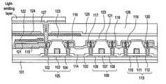
- FIG. 1is a view showing a cross section of a liquid crystal panel
- FIG. 2is a view showing the Raman spectrum of a DLC film
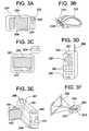
- FIGS. 3A to 3 Fare views schematically showing devices using the present invention.
- a DLC film 125is provided on an interlayer insulating film 123 and a shielding titanium film 124 .
- the DLC filmeffectively releases heat generated by a pixel TFT 105 , and TFTs 109 , 113 constituting a peripheral driving circuit.
- FIG. 1schematically shows a cross section of a reflection type liquid crystal panel using the present invention.
- reference numeral 101denotes a glass substrate.
- a quartz substratemay be used instead of the glass substrate.
- An NTFT 105N-channel thin film transistor, also called a pixel TFT
- a PTFT 109 and an NTFT 113 constituting a peripheral driving circuitare disposed on the glass substrate 101 .
- a drain region 102 , a channel region 103 , and a source region 104are formed in the NTFT 105 .
- a source region 106 , a channel region 107 , and a drain region 108are formed in the PTFT 109 .
- a source region 112 , a channel region 111 , and a drain region 110are formed in the NTFT 113 .
- the thickness of an active layer of the respective TFTsis made 50 nm.
- a silicon oxide film with a thickness of 100 nm as a common gate insulating filmis provided in the respective TFTs.
- the respective TFTsare covered with a silicon oxide film 114 with a thickness of 700 ⁇ m as an interlayer insulating film.
- a source electrode 117 brought into contact with the source region 106 of the PTFT 109 constituting the peripheral driving circuit, and a drain electrode 118 brought into contact with the drain region 108 of the PTFT 109are disposed.
- a source electrode 120 brought into contact with the source region 112 of the NTFT 113 constituting the peripheral driving circuit, a drain electrode 119 brought into contact with the drain region 110 of the NTFT 113are disposed.
- a titanium film with a thickness of 100 nmis formed over and under the electrodes and wiring lines designated by 115 , 116 , 117 , 118 , 119 , and 120 . This film is necessary so as to have an excellent contact.
- a silicon nitride film 121 with a thickness of 50 nmis formed to cover the electrodes and wiring lines designated by 115 , 116 , 117 , 118 , 119 , and 120 .
- a pattern 122 made of a titanium filmis formed.
- a capacitanceis formed by the pattern 122 made of the titanium film and the drain electrode 115 through the silicon nitride film 121 .
- Reference numeral 123denotes a polyimide resin film with a thickness of 800 nm. This resin film is provided to absorb roughness formed by the existence of the TFTs, the electrodes, and the wiring lines so that a flattened surface is produced.
- Resin materialsuch as polyimide amide, polyamide, acryl, and epoxy may be used other than polyimide.
- An electromagnetic shielding pattern 124 made of a titanium film with a thickness of 100 nmis disposed on the interlayer insulating film 123 .
- This electromagnetic shielding patternis disposed so that a reflecting pixel electrode 127 does not interfere with the source wiring line and the TFT.
- a DLC (Diamond-like Carbon) 125 with a thickness of 1000 nmis formed.
- the DLC filmit is preferable to use a film which exhibits the Raman spectrum as shown in FIG. 2 .
- the DLC filmcan be easily formed on the resin material, and has high heat conductivity, the DLC film effectively functions as a heat sink especially for diffusing heat generated by the TFTs of the peripheral driving circuit.
- an AlN film and a diamond film other than the DLC filmmay be exemplified as a thin film that can be used as a heat sink, the DLC film can be most easily formed on a resin material.
- a polyimide resin film 126 with an average thickness of 1 ⁇ m as an interlayer insulating filmis formed on the DLC film, and further the reflecting pixel electrode 127 having a thickness of 400 nm and made of aluminum, is provided.
- a top-gate type TFTis shown, a bottom-gate type TFT may be adopted.
- FIG. 3Ashows a portable information processing terminal, which has a communication function using telephone lines.
- This deviceincludes an integrated circuit 2006 in the inside of a main body 2001 . Further, this device includes a reflection type active matrix liquid crystal panel 2005 in which TFTs as switching elements are disposed, a camera portion 2002 for incorporating a picture image, and an operation switch 2004 .
- FIG. 3Bshows an electric device called a head mount display.
- This devicehas a function to display a false picture image in front of eyes when a main body 2101 is mounted on a head through a band 2103 .
- the picture imageis formed by active matrix type liquid crystal panels 2102 corresponding to right and left eyes.
- FIG. 3Cshows an electric device having a function to display map information and various kinds of information based on signals from an artificial satellite.
- Information from an artificial satelliteis received by an antenna 2204 , and is processed by an electric circuit provided in the inside of a main body 2201 , and necessary information is displayed on an active matrix type reflection type liquid crystal panel 2202 .
- the operation of the deviceis carried out by an operation switch 2203 . Even in such a device, a circuit using TFTs is used.
- FIG. 3Dshows a portable telephone.
- This electric deviceincludes a main body 2301 , an antenna 2306 , an audio output portion 2302 , a liquid crystal panel 2304 , an operation switch 2305 , and an audio input portion 2303 .
- FIG. 3Eshows a portable imaging device called a video camera.
- This deviceincludes a reflection type liquid crystal panel 2402 attached to a close-open member of a main body 2401 , and an operation switch 2404 attached to the close-open member.
- the main body 2401is provided with an image receiving portion 2406 , an integrated circuit 2407 , an audio input portion 2403 , an operation switch 2404 , and a battery 2405 .
- FIG. 3Fshows a projection type liquid crystal display device.
- This deviceincludes a main body 2501 provided with a light source 2502 , a reflection type liquid crystal panel 2503 , and an optical system 2504 , and has a function to project a picture image onto a screen 2505 .
- the present inventioncan also be used for a flat panel display other than the case of using a liquid crystal.
- a liquid crystalFor example, in an EL display, the present invention can be used when an under layer of a light emitting layer is flattened.
- the present inventioncan also be used for an EC display and the like.
- the present inventioncan be used for realizing the structure in which a surface over a pixel region is desired to be flat.
Landscapes
- Physics & Mathematics (AREA)
- Nonlinear Science (AREA)
- Mathematical Physics (AREA)
- Chemical & Material Sciences (AREA)
- Crystallography & Structural Chemistry (AREA)
- General Physics & Mathematics (AREA)
- Optics & Photonics (AREA)
- Engineering & Computer Science (AREA)
- Microelectronics & Electronic Packaging (AREA)
- Liquid Crystal (AREA)
- Devices For Indicating Variable Information By Combining Individual Elements (AREA)
- Thin Film Transistor (AREA)
Abstract
Description
- 1. Field of the Invention
- The present invention relates to the structure of a reflection type liquid crystal display device.
- 2. Description of the Related Art
- A reflection type liquid crystal panel has been known. Also, in an active matrix type liquid crystal panel, there is known a structure in which a peripheral driving circuit is integrated on the same substrate as an active matrix circuit. This structure is known as a peripheral driving circuit integration type.
- In a peripheral driving circuit integration type liquid crystal panel, as a result that high picture quality is pursued, a peripheral driving circuit is required to operate at such a high speed as several tens MHz or more.
- However, high speed operation causes a problem of heat generation from a device. Especially, since a liquid crystal panel uses a glass substrate or a quartz substrate, the panel has a problem that there is no escape for heat generated by a device (the thermal conductivity of quartz is 1/100 or less than that of single crystal silicon).
- Also, a reflection type liquid crystal display panel is easy to secure a required aperture factor even if it is miniaturized. Accordingly, it has been considered to use the display panel for a projection type display.
- However, since a liquid crystal panel for a projector is miniaturized (about 3 inches or less in diagonal), the above described problem of heat generation (heat generation from a peripheral driving circuit) especially becomes important.
- Specifically, the peripheral driving circuit has such problems that the device characteristic is changed or deteriorated, or the device itself is broken by the heat generated by the circuit itself.
- An object of the present invention is therefore to provide a structure of a display device capable of solving this sort of problem.
- According to one aspect of the present invention, a display device is comprised of a pixel matrix portion; a peripheral driving circuit portion disposed on the same substrate as the pixel matrix portion; a thin film transistor disposed in each of the pixel matrix portion and the peripheral driving circuit portion; an interlayer insulating film made of resin material and disposed over the thin film transistor; and a carbon film disposed on the interlayer insulating film.
- According to another aspect of the present invention, a display device is comprised of a pixel matrix portion; a peripheral driving circuit portion disposed on the same substrate as the pixel matrix portion; a thin film transistor disposed in each of the pixel matrix portion and the peripheral driving circuit portion, an interlayer insulating film made of resin material and disposed over the thin film transistor; and a carbon film as a heat releasing layer disposed on the interlayer insulating film.
- It is preferable to use a DLC (Diamond-like Carbon) film as the carbon film. The DLC film is a carbon film comprising amorphous carbon having SP3bonds.
- In the accompanying drawings:
FIG. 1 is a view showing a cross section of a liquid crystal panel;FIG. 2 is a view showing the Raman spectrum of a DLC film; andFIGS. 3A to3F are views schematically showing devices using the present invention.- According to the present invention, as shown in
FIG. 1 , aDLC film 125 is provided on an interlayerinsulating film 123 and ashielding titanium film 124. The DLC film effectively releases heat generated by apixel TFT 105, andTFTs FIG. 1 schematically shows a cross section of a reflection type liquid crystal panel using the present invention. In the drawing,reference numeral 101 denotes a glass substrate. A quartz substrate may be used instead of the glass substrate.- An NTFT105 (N-channel thin film transistor, also called a pixel TFT) disposed in an active matrix circuit, and a
PTFT 109 and an NTFT113 constituting a peripheral driving circuit are disposed on theglass substrate 101. - A
drain region 102, achannel region 103, and asource region 104 are formed in the NTFT105. - A
source region 106, achannel region 107, and adrain region 108 are formed in the PTFT109. - A
source region 112, achannel region 111, and adrain region 110 are formed in the NTFT113. - The thickness of an active layer of the respective TFTs is made 50 nm. A silicon oxide film with a thickness of 100 nm as a common gate insulating film is provided in the respective TFTs.
- The respective TFTs are covered with a
silicon oxide film 114 with a thickness of 700 μm as an interlayer insulating film. - A
source wiring line 116 brought into contact with thesource region 104 of the NTFT105, and adrain electrode 115 brought into contact with the drain region of the NTFT105, each made of an aluminum film with a thickness of 500 nm, are disposed on theinterlayer insulating film 114. - Also, a
source electrode 117 brought into contact with thesource region 106 of the PTFT109 constituting the peripheral driving circuit, and adrain electrode 118 brought into contact with thedrain region 108 of thePTFT 109 are disposed. - Also, a
source electrode 120 brought into contact with thesource region 112 of the NTFT113 constituting the peripheral driving circuit, adrain electrode 119 brought into contact with thedrain region 110 of the NTFT113 are disposed. - A titanium film with a thickness of 100 nm is formed over and under the electrodes and wiring lines designated by115,116,117,118,119, and120. This film is necessary so as to have an excellent contact.
- A
silicon nitride film 121 with a thickness of 50 nm is formed to cover the electrodes and wiring lines designated by115,116,117,118,119, and120. - Further, a
pattern 122 made of a titanium film is formed. A capacitance is formed by thepattern 122 made of the titanium film and thedrain electrode 115 through thesilicon nitride film 121. Reference numeral 123 denotes a polyimide resin film with a thickness of 800 nm. This resin film is provided to absorb roughness formed by the existence of the TFTs, the electrodes, and the wiring lines so that a flattened surface is produced.- Resin material such as polyimide amide, polyamide, acryl, and epoxy may be used other than polyimide.
- An
electromagnetic shielding pattern 124 made of a titanium film with a thickness of 100 nm is disposed on the interlayerinsulating film 123. This electromagnetic shielding pattern is disposed so that a reflectingpixel electrode 127 does not interfere with the source wiring line and the TFT. - A DLC (Diamond-like Carbon)125 with a thickness of 1000 nm is formed.
- As the DLC film, it is preferable to use a film which exhibits the Raman spectrum as shown in
FIG. 2 . - Since the DLC film can be easily formed on the resin material, and has high heat conductivity, the DLC film effectively functions as a heat sink especially for diffusing heat generated by the TFTs of the peripheral driving circuit.
- In a reflection type liquid crystal panel, there is no problem even if the DLC film extends to a pixel matrix portion. The adoption of such a structure enables the film to deal with heat generation from not only the peripheral driving circuit but also the pixel matrix portion.
- Incidentally, although an AlN film and a diamond film other than the DLC film may be exemplified as a thin film that can be used as a heat sink, the DLC film can be most easily formed on a resin material.
- A
polyimide resin film 126 with an average thickness of 1 μm as an interlayer insulating film is formed on the DLC film, and further the reflectingpixel electrode 127 having a thickness of 400 nm and made of aluminum, is provided. - In this embodiment, although a top-gate type TFT is shown, a bottom-gate type TFT may be adopted.
- In this embodiment, examples of display devices using the reflection type liquid crystal panel obtained by using the present invention will be described.
FIG. 3A shows a portable information processing terminal, which has a communication function using telephone lines.- This device includes an
integrated circuit 2006 in the inside of amain body 2001. Further, this device includes a reflection type active matrixliquid crystal panel 2005 in which TFTs as switching elements are disposed, acamera portion 2002 for incorporating a picture image, and anoperation switch 2004. FIG. 3B shows an electric device called a head mount display. This device has a function to display a false picture image in front of eyes when amain body 2101 is mounted on a head through aband 2103. The picture image is formed by active matrix typeliquid crystal panels 2102 corresponding to right and left eyes.FIG. 3C shows an electric device having a function to display map information and various kinds of information based on signals from an artificial satellite. Information from an artificial satellite is received by anantenna 2204, and is processed by an electric circuit provided in the inside of amain body 2201, and necessary information is displayed on an active matrix type reflection typeliquid crystal panel 2202.- The operation of the device is carried out by an
operation switch 2203. Even in such a device, a circuit using TFTs is used. FIG. 3D shows a portable telephone. This electric device includes amain body 2301, anantenna 2306, anaudio output portion 2302, aliquid crystal panel 2304, anoperation switch 2305, and anaudio input portion 2303.FIG. 3E shows a portable imaging device called a video camera. This device includes a reflection typeliquid crystal panel 2402 attached to a close-open member of amain body 2401, and anoperation switch 2404 attached to the close-open member.- Further, the
main body 2401 is provided with animage receiving portion 2406, anintegrated circuit 2407, anaudio input portion 2403, anoperation switch 2404, and abattery 2405. FIG. 3F shows a projection type liquid crystal display device. This device includes amain body 2501 provided with alight source 2502, a reflection typeliquid crystal panel 2503, and anoptical system 2504, and has a function to project a picture image onto ascreen 2505.- It should be noted that the present invention can also be used for a flat panel display other than the case of using a liquid crystal. For example, in an EL display, the present invention can be used when an under layer of a light emitting layer is flattened. The present invention can also be used for an EC display and the like.
- That is, the present invention can be used for realizing the structure in which a surface over a pixel region is desired to be flat.
- As described above, by using the present invention, it is possible to provide a structure in which heat generated by a peripheral driving circuit can be effectively radiated. Also it is possible to provide a structure in which heat generated in the inside of a liquid crystal panel can be effectively radiated.
Claims (29)
1. A display device comprising:
a substrate;
a thin film transistor formed over the substrate;
a first insulating film formed over the thin film transistor, the first insulating film having a first contact hole;
an electrode formed over the first insulating film, the electrode being in contact with one of a source region or a drain region of the thin film transistor through the first contact hole;
a second insulating film formed over the electrode, the second insulating film comprising silicon nitride and having a second contact hole; and
a pixel electrode formed over the second insulating film, the pixel electrode being in contact with the electrode through the second contact hole,
wherein the second contact hole is overlapped with the first contact hole.
2. A display device comprising:
a substrate;
a thin film transistor formed over the substrate;
a first insulating film formed over the thin film transistor, the first insulating film having a first contact hole;
an electrode formed over the first insulating film, the electrode being in contact with one of a source region or a drain region of the thin film transistor through the first contact hole;
a second insulating film formed over the electrode, the second insulating film comprising silicon nitride and having a second contact hole;
a third insulating film formed over the second insulating film, the third insulating film comprising an organic resin and having a third contact hole; and
a pixel electrode formed over the third insulating film, the pixel electrode being in contact with the electrode through the second contact hole and the third contact hole,
wherein the second contact hole and the third contact hole are overlapped with the first contact hole.
3. A display device comprising:
a substrate;
a thin film transistor formed over the substrate;
a first insulating film formed over the thin film transistor, the first insulating film having a first contact hole;
an electrode formed over the first insulating film, the electrode being in contact with one of a source region or a drain region of the thin film transistor through the first contact hole;
a second insulating film formed over the electrode, the second insulating film comprising silicon nitride and having a second contact hole;
a third insulating film formed over the second insulating film, the third insulating film having a third contact hole; and
a pixel electrode formed over the third insulating film, the pixel electrode being in contact with the electrode through the second contact hole and the third contact hole,
wherein the second contact hole and the third contact hole are overlapped with the first contact hole, and
wherein size of the third contact hole is larger than that of the second contact hole.
4. The display device according toclaim 1 , wherein the thin film transistor is a top-gate type thin film transistor.
5. The display device according toclaim 2 , wherein the thin film transistor is a top-gate type thin film transistor.
6. The display device according toclaim 3 , wherein the thin film transistor is a top-gate type thin film transistor.
7. The display device according toclaim 1 , wherein the electrode comprises a titanium film, an aluminum film and a titanium film.
8. The display device according toclaim 2 , wherein the electrode comprises a titanium film, an aluminum film and a titanium film.
9. The display device according toclaim 3 , wherein the electrode comprises a titanium film, an aluminum film and a titanium film.
10. The display device according toclaim 1 , wherein the first insulating film comprises silicon oxide film.
11. The display device according toclaim 2 , wherein the first insulating film comprises silicon oxide film.
12. The display device according toclaim 3 , wherein the first insulating film comprises silicon oxide film.
13. The display device according toclaim 1 , wherein the pixel electrode is a reflecting pixel electrode.
14. The display device according toclaim 2 , wherein the pixel electrode is a reflecting pixel electrode.
15. The display device according toclaim 3 , wherein the pixel electrode is a reflecting pixel electrode.
16. The display device according toclaim 1 , wherein the display device is a liquid crystal panel.
17. The display device according toclaim 2 , wherein the display device is a liquid crystal panel.
18. The display device according toclaim 3 , wherein the display device is a liquid crystal panel.
19. An electric device having the display device according toclaim 1 , wherein the electric device is one selected from the group consisting of a portable information processing terminal, a head mount display, a portable telephone, a video camera and a projector.
20. An electric device having the display device according toclaim 2 , wherein the electric device is one selected from the group consisting of a portable information processing terminal, a head mount display, a portable telephone, a video camera and a projector.
21. An electric device having the display device according toclaim 3 , wherein the electric device is one selected from the group consisting of a portable information processing terminal, a head mount display, a portable telephone, a video camera and a projector.
22. The display device according toclaim 1 , further comprising:
a light emitting layer formed over the pixel electrode.
23. The display device according toclaim 2 , further comprising:
a light emitting layer formed over the pixel electrode.
24. The display device according toclaim 3 , further comprising:
a light emitting layer formed over the pixel electrode.
25. The display device according toclaim 22 , wherein the display device is an EL display.
26. The display device according toclaim 23 , wherein the display device is an EL display.
27. The display device according toclaim 24 , wherein the display device is an EL display.
28. The display device according toclaim 2 , wherein the organic resin is one selected from the group consisting of polyimide, polyimideamide, polyamide, acryl and epoxy.
29. The display device according toclaim 3 , wherein the third insulating film comprises a diamond-like carbon film.
Priority Applications (1)
| Application Number | Priority Date | Filing Date | Title |
|---|---|---|---|
| US11/648,571US7436463B2 (en) | 1997-03-26 | 2007-01-03 | Display device |
Applications Claiming Priority (7)
| Application Number | Priority Date | Filing Date | Title |
|---|---|---|---|
| JP9-092935 | 1997-03-26 | ||
| JP9092935AJPH10268360A (en) | 1997-03-26 | 1997-03-26 | Display device |
| US09/045,697US6115090A (en) | 1997-03-26 | 1998-03-23 | Display device |
| US09/295,397US6593990B1 (en) | 1997-03-26 | 1999-04-21 | Display device |
| US09/748,166US6927826B2 (en) | 1997-03-26 | 2000-12-27 | Display device |
| US11/187,809US7190428B2 (en) | 1997-03-26 | 2005-07-25 | Display device |
| US11/648,571US7436463B2 (en) | 1997-03-26 | 2007-01-03 | Display device |
Related Parent Applications (1)
| Application Number | Title | Priority Date | Filing Date |
|---|---|---|---|
| US11/187,809DivisionUS7190428B2 (en) | 1997-03-26 | 2005-07-25 | Display device |
Publications (2)
| Publication Number | Publication Date |
|---|---|
| US20070263133A1true US20070263133A1 (en) | 2007-11-15 |
| US7436463B2 US7436463B2 (en) | 2008-10-14 |
Family
ID=26434295
Family Applications (3)
| Application Number | Title | Priority Date | Filing Date |
|---|---|---|---|
| US09/748,166Expired - Fee RelatedUS6927826B2 (en) | 1997-03-26 | 2000-12-27 | Display device |
| US11/187,809Expired - Fee RelatedUS7190428B2 (en) | 1997-03-26 | 2005-07-25 | Display device |
| US11/648,571Expired - Fee RelatedUS7436463B2 (en) | 1997-03-26 | 2007-01-03 | Display device |
Family Applications Before (2)
| Application Number | Title | Priority Date | Filing Date |
|---|---|---|---|
| US09/748,166Expired - Fee RelatedUS6927826B2 (en) | 1997-03-26 | 2000-12-27 | Display device |
| US11/187,809Expired - Fee RelatedUS7190428B2 (en) | 1997-03-26 | 2005-07-25 | Display device |
Country Status (1)
| Country | Link |
|---|---|
| US (3) | US6927826B2 (en) |
Cited By (3)
| Publication number | Priority date | Publication date | Assignee | Title |
|---|---|---|---|---|
| US20040178726A1 (en)* | 2001-02-19 | 2004-09-16 | Semiconductor Energy Laboratory Co., Ltd. | Light emitting device and manufacturing method thereof |
| US7633085B2 (en) | 1999-03-29 | 2009-12-15 | Semiconductor Energy Laboratory Co., Ltd. | Semiconductor device and manufacturing method thereof |
| US20130087800A1 (en)* | 2011-10-07 | 2013-04-11 | Pil Soon HONG | Thin film transistor array panel and manufacturing method thereof |
Families Citing this family (28)
| Publication number | Priority date | Publication date | Assignee | Title |
|---|---|---|---|---|
| US6294799B1 (en)* | 1995-11-27 | 2001-09-25 | Semiconductor Energy Laboratory Co., Ltd. | Semiconductor device and method of fabricating same |
| US5940732A (en) | 1995-11-27 | 1999-08-17 | Semiconductor Energy Laboratory Co., | Method of fabricating semiconductor device |
| US6927826B2 (en)* | 1997-03-26 | 2005-08-09 | Semiconductor Energy Labaratory Co., Ltd. | Display device |
| JPH11307782A (en)* | 1998-04-24 | 1999-11-05 | Semiconductor Energy Lab Co Ltd | Semiconductor device and manufacturing method thereof |
| US7288420B1 (en) | 1999-06-04 | 2007-10-30 | Semiconductor Energy Laboratory Co., Ltd. | Method for manufacturing an electro-optical device |
| TWI232595B (en) | 1999-06-04 | 2005-05-11 | Semiconductor Energy Lab | Electroluminescence display device and electronic device |
| US6563482B1 (en) | 1999-07-21 | 2003-05-13 | Semiconductor Energy Laboratory Co., Ltd. | Display device |
| US6587086B1 (en) | 1999-10-26 | 2003-07-01 | Semiconductor Energy Laboratory Co., Ltd. | Electro-optical device |
| JP3823016B2 (en)* | 2000-07-21 | 2006-09-20 | 株式会社日立製作所 | Liquid crystal display |
| US6734924B2 (en) | 2000-09-08 | 2004-05-11 | Semiconductor Energy Laboratory Co., Ltd. | Liquid crystal display device |
| US7462372B2 (en)* | 2000-09-08 | 2008-12-09 | Semiconductor Energy Laboratory Co., Ltd. | Light emitting device, method of manufacturing the same, and thin film forming apparatus |
| DE10046411A1 (en)* | 2000-09-18 | 2002-03-28 | Philips Corp Intellectual Pty | Projection device with liquid crystal light modulator |
| US6664732B2 (en)* | 2000-10-26 | 2003-12-16 | Semiconductor Energy Laboratory Co., Ltd. | Light emitting device and manufacturing method thereof |
| TW522577B (en)* | 2000-11-10 | 2003-03-01 | Semiconductor Energy Lab | Light emitting device |
| US6980272B1 (en) | 2000-11-21 | 2005-12-27 | Sarnoff Corporation | Electrode structure which supports self alignment of liquid deposition of materials |
| TW588570B (en)* | 2001-06-18 | 2004-05-21 | Semiconductor Energy Lab | Light emitting device and method of fabricating the same |
| CN100380673C (en)* | 2001-11-09 | 2008-04-09 | 株式会社半导体能源研究所 | Light emitting device and manufacturing method thereof |
| US7042024B2 (en)* | 2001-11-09 | 2006-05-09 | Semiconductor Energy Laboratory Co., Ltd. | Light emitting apparatus and method for manufacturing the same |
| US6822264B2 (en)* | 2001-11-16 | 2004-11-23 | Semiconductor Energy Laboratory Co., Ltd. | Light emitting device |
| JP4199501B2 (en)* | 2002-09-13 | 2008-12-17 | Nec液晶テクノロジー株式会社 | Manufacturing method of liquid crystal display device |
| US20040124421A1 (en)* | 2002-09-20 | 2004-07-01 | Semiconductor Energy Laboratory Co., Ltd. | Light-emitting device and manufacturing method thereof |
| JP4095518B2 (en)* | 2002-10-31 | 2008-06-04 | セイコーエプソン株式会社 | Electro-optical device and electronic apparatus |
| KR101759639B1 (en)* | 2010-12-29 | 2017-07-21 | 삼성디스플레이 주식회사 | Organic electroluminescence display module |
| JP2012243935A (en)* | 2011-05-19 | 2012-12-10 | Sony Corp | Device and display apparatus |
| KR20150053314A (en) | 2013-11-07 | 2015-05-18 | 삼성디스플레이 주식회사 | Thin film transistor and display device having the same |
| US9105615B1 (en) | 2014-06-12 | 2015-08-11 | Amazon Technologies, Inc. | Substrate vias for a display device |
| JP2018120123A (en)* | 2017-01-26 | 2018-08-02 | 株式会社ジャパンディスプレイ | Display device and inter-substrate conduction structure |
| KR102405404B1 (en)* | 2017-06-13 | 2022-06-07 | 삼성디스플레이 주식회사 | Display device and methed of manufacturing the display device |
Citations (71)
| Publication number | Priority date | Publication date | Assignee | Title |
|---|---|---|---|---|
| US4254426A (en)* | 1979-05-09 | 1981-03-03 | Rca Corporation | Method and structure for passivating semiconductor material |
| US4448491A (en)* | 1979-08-08 | 1984-05-15 | Canon Kabushiki Kaisha | Image display apparatus |
| US4650922A (en)* | 1985-03-11 | 1987-03-17 | Texas Instruments Incorporated | Thermally matched mounting substrate |
| US4705358A (en)* | 1985-06-10 | 1987-11-10 | Seiko Instruments & Electronics Ltd. | Substrate for active matrix display |
| US4722913A (en)* | 1986-10-17 | 1988-02-02 | Thomson Components-Mostek Corporation | Doped semiconductor vias to contacts |
| US4804490A (en)* | 1987-10-13 | 1989-02-14 | Energy Conversion Devices, Inc. | Method of fabricating stabilized threshold switching material |
| US4845533A (en)* | 1986-08-22 | 1989-07-04 | Energy Conversion Devices, Inc. | Thin film electrical devices with amorphous carbon electrodes and method of making same |
| US4869755A (en)* | 1987-07-30 | 1989-09-26 | Nukem Gmbh | Encapsulation of a photovoltaic element |
| US4972250A (en)* | 1987-03-02 | 1990-11-20 | Microwave Technology, Inc. | Protective coating useful as passivation layer for semiconductor devices |
| US5101288A (en)* | 1989-04-06 | 1992-03-31 | Ricoh Company, Ltd. | LCD having obliquely split or interdigitated pixels connected to MIM elements having a diamond-like insulator |
| US5117299A (en)* | 1989-05-20 | 1992-05-26 | Ricoh Company, Ltd. | Liquid crystal display with a light blocking film of hard carbon |
| US5176791A (en)* | 1988-08-11 | 1993-01-05 | Semiconductor Energy Laboratory Co., Ltd. | Method for forming carbonaceous films |
| US5196954A (en)* | 1985-08-08 | 1993-03-23 | Semiconductor Energy Laboratory Co., Ltd. | Liquid crystal display |
| US5250451A (en)* | 1991-04-23 | 1993-10-05 | France Telecom Etablissement Autonome De Droit Public | Process for the production of thin film transistors |
| US5330616A (en)* | 1988-02-01 | 1994-07-19 | Semiconductor Energy Laboratory Co., Ltd. | Electric device provided with carbon pattern structure and manufacturing method for the same |
| US5392143A (en)* | 1989-11-30 | 1995-02-21 | Kabushiki Kaisha Toshiba | Liquid crystal display having drain and pixel electrodes linkable to a wiring line having a potential |
| US5422658A (en)* | 1990-02-09 | 1995-06-06 | Sharp Kabushiki Kaisha | Driving method and a driving device for a display device |
| US5432527A (en)* | 1990-05-07 | 1995-07-11 | Fujitsu Limited | High quality active matrix-type display device |
| US5461501A (en)* | 1992-10-08 | 1995-10-24 | Hitachi, Ltd. | Liquid crystal substrate having 3 metal layers with slits offset to block light from reaching the substrate |
| US5536950A (en)* | 1994-10-28 | 1996-07-16 | Honeywell Inc. | High resolution active matrix LCD cell design |
| US5550066A (en)* | 1994-12-14 | 1996-08-27 | Eastman Kodak Company | Method of fabricating a TFT-EL pixel |
| US5572046A (en)* | 1993-06-30 | 1996-11-05 | Semiconductor Energy Laboratory Co., Ltd. | Semiconductor device having at least two thin film transistors |
| US5583369A (en)* | 1992-07-06 | 1996-12-10 | Semiconductor Energy Laboratory Co., Ltd. | Semiconductor device and method for forming the same |
| US5585951A (en)* | 1992-12-25 | 1996-12-17 | Sony Corporation | Active-matrix substrate |
| US5621556A (en)* | 1994-04-28 | 1997-04-15 | Xerox Corporation | Method of manufacturing active matrix LCD using five masks |
| US5652029A (en)* | 1994-03-25 | 1997-07-29 | Semiconductor Energy Laboratory Co., Ltd. | Plasma processing apparatus and plasma processing method |
| US5686328A (en)* | 1993-07-14 | 1997-11-11 | Semiconductor Energy Laboratory Co., Ltd. | Semiconductor device and process for fabricating the same |
| US5686980A (en)* | 1995-04-03 | 1997-11-11 | Kabushiki Kaisha Toshiba | Light-shielding film, useable in an LCD, in which fine particles of a metal or semi-metal are dispersed in and throughout an inorganic insulating film |
| US5696386A (en)* | 1993-02-10 | 1997-12-09 | Semiconductor Energy Laboratory Co. Ltd. | Semiconductor device |
| US5706067A (en)* | 1995-04-28 | 1998-01-06 | International Business Machines Corporation | Reflective spatial light modulator array |
| US5712495A (en)* | 1994-06-13 | 1998-01-27 | Semiconductor Energy Laboratory Co., Ltd. | Semiconductor device including active matrix circuit |
| US5717224A (en)* | 1994-04-29 | 1998-02-10 | Semiconductor Energy Laboratory Co., Ltd. | Semiconductor device having an insulated gate field effect thin film transistor |
| US5724107A (en)* | 1994-09-30 | 1998-03-03 | Sanyo Electric Co., Ltd. | Liquid crystal display with transparent storage capacitors for holding electric charges |
| US5739549A (en)* | 1994-06-14 | 1998-04-14 | Semiconductor Energy Laboratory Co., Ltd. | Thin film transistor having offset region |
| US5747830A (en)* | 1995-09-14 | 1998-05-05 | Canon Kabushiki Kaisha | Semiconductor display device with a hydrogen supply and hydrogen diffusion barrier layers |
| US5748165A (en)* | 1993-12-24 | 1998-05-05 | Sharp Kabushiki Kaisha | Image display device with plural data driving circuits for driving the display at different voltage magnitudes and polarity |
| US5777701A (en)* | 1995-05-08 | 1998-07-07 | Semiconductor Energy Laboratory Co., Ltd. | Display device |
| US5784201A (en)* | 1995-03-17 | 1998-07-21 | Lg Electronics Inc. | Reflection-preventing layer for a display device |
| US5808315A (en)* | 1992-07-21 | 1998-09-15 | Semiconductor Energy Laboratory Co., Ltd. | Thin film transistor having transparent conductive film |
| US5815231A (en)* | 1995-12-19 | 1998-09-29 | Semiconductor Energy Laboratory Co., Ltd. | Liquid crystal display and method of manufacturing the same |
| US5818550A (en)* | 1994-10-19 | 1998-10-06 | Sony Corporation | Color display device |
| US5820947A (en)* | 1994-05-17 | 1998-10-13 | Semicondutor Energy Laboratory Co., Ltd. | Plasma processing method and apparatus |
| US5847410A (en)* | 1995-11-24 | 1998-12-08 | Semiconductor Energy Laboratory Co. | Semiconductor electro-optical device |
| US5851862A (en)* | 1994-03-11 | 1998-12-22 | Semiconductor Energy Laboratory Co., Ltd. | Method of crystallizing a silicon film |
| US5871847A (en)* | 1988-03-07 | 1999-02-16 | Semiconductor Energy Laboratory Co., Ltd. | Electrostatic-erasing abrasion-proof coating and method for forming the same |
| US5879741A (en)* | 1993-03-24 | 1999-03-09 | Semiconductor Energy Laboratory Co., Ltd. | Apparatus and method for forming film |
| US5926242A (en)* | 1996-07-15 | 1999-07-20 | Sony Corporation | Active matrix reflective guest-host LCD with pixel electrodes patterned on quarter wave plate |
| US5952708A (en)* | 1995-11-17 | 1999-09-14 | Semiconductor Energy Laboratory Co., Ltd. | Display device |
| US5963278A (en)* | 1991-03-26 | 1999-10-05 | Semiconductor Energy Laboratory Co., Ltd. | Electro-optical device and method for driving the same |
| US5989672A (en)* | 1992-11-19 | 1999-11-23 | Semiconductor Energy Laboratory Co., Ltd. | Magnetic recording medium |
| US5990542A (en)* | 1995-12-14 | 1999-11-23 | Semiconductor Energy Laboratory Co., Ltd. | Semiconductor device |
| US5995189A (en)* | 1995-12-21 | 1999-11-30 | Semiconductor Energy Laboratory Co., Ltd. | Liquid-crystal display device |
| US6001431A (en)* | 1992-12-28 | 1999-12-14 | Semiconductor Energy Laboratory Co., Ltd. | Process for fabricating a magnetic recording medium |
| US6005648A (en)* | 1996-06-25 | 1999-12-21 | Semiconductor Energy Laboratory Co., Ltd. | Display device |
| US6055034A (en)* | 1996-06-25 | 2000-04-25 | Semiconductor Energy Laboratory Co., Ltd. | Liquid crystal display panel |
| US6097459A (en)* | 1994-10-03 | 2000-08-01 | Sharp Kabushiki Kaisha | Method for producing a reflection type liquid crystal display |
| US6110542A (en)* | 1990-09-25 | 2000-08-29 | Semiconductor Energy Laboratory Co., Ltd. | Method for forming a film |
| US6115090A (en)* | 1997-03-26 | 2000-09-05 | Semiconductor Energy Laboratory Co., Ltd. | Display device |
| US6114715A (en)* | 1996-11-29 | 2000-09-05 | Sanyo Electric Co., Ltd. | Display apparatus using electroluminescence elements |
| US6133073A (en)* | 1996-02-23 | 2000-10-17 | Semiconductor Energy Laboratory Co., Ltd. | Thin film semiconductor and method for manufacturing the same, semiconductor device and method for manufacturing the same |
| US6163055A (en)* | 1997-03-24 | 2000-12-19 | Semiconductor Energy Laboratory Co., Ltd | Semiconductor device and manufacturing method thereof |
| US6171674B1 (en)* | 1993-07-20 | 2001-01-09 | Semiconductor Energy Laboratory Co., Ltd. | Hard carbon coating for magnetic recording medium |
| US6217661B1 (en)* | 1987-04-27 | 2001-04-17 | Semiconductor Energy Laboratory Co., Ltd. | Plasma processing apparatus and method |
| US6224952B1 (en)* | 1988-03-07 | 2001-05-01 | Semiconductor Energy Laboratory Co., Ltd. | Electrostatic-erasing abrasion-proof coating and method for forming the same |
| US6249330B1 (en)* | 1997-09-30 | 2001-06-19 | Sanyo Electric Co., Ltd. | Display device and manufacturing method |
| US6252297B1 (en)* | 1997-03-07 | 2001-06-26 | Kabushiki Kaisha Toshiba | Array substrate, liquid crystal display device and their manufacturing method |
| US6323918B1 (en)* | 1996-12-10 | 2001-11-27 | Fujitsu Limited | Liquid crystal display device and process for production thereof |
| US6596990B2 (en)* | 2000-06-10 | 2003-07-22 | Bruker Daltonik Gmbh | Internal detection of ions in quadrupole ion traps |
| US6621535B1 (en)* | 1998-04-24 | 2003-09-16 | Semiconductor Energy Laboratory Co., Ltd. | Semiconductor device and method of manufacturing the same |
| US6927826B2 (en)* | 1997-03-26 | 2005-08-09 | Semiconductor Energy Labaratory Co., Ltd. | Display device |
| US6982768B2 (en)* | 1996-02-20 | 2006-01-03 | Semiconductor Energy Laboratory Co., Ltd. | Liquid crystal display device |
Family Cites Families (21)
| Publication number | Priority date | Publication date | Assignee | Title |
|---|---|---|---|---|
| US18097A (en)* | 1857-09-01 | Hub fob carriage-wheels | ||
| JPS55107270A (en) | 1979-02-09 | 1980-08-16 | Nec Corp | Manufacture of field-effect transistor |
| JPS58145134A (en) | 1982-02-23 | 1983-08-29 | Seiko Epson Corp | semiconductor equipment |
| JPS60145375A (en) | 1984-01-09 | 1985-07-31 | Nippon Telegr & Teleph Corp <Ntt> | Method for passivating surface of nb film |
| JPS61204933A (en) | 1985-03-08 | 1986-09-11 | Fujitsu Ltd | Manufacture of semiconductor device |
| JPH0666471B2 (en) | 1985-04-20 | 1994-08-24 | 沖電気工業株式会社 | Thin film transistor |
| EP0221531A3 (en) | 1985-11-06 | 1992-02-19 | Kanegafuchi Kagaku Kogyo Kabushiki Kaisha | High heat conductive insulated substrate and method of manufacturing the same |
| JPS6315461A (en) | 1986-07-08 | 1988-01-22 | Seiko Epson Corp | Solid-state image sensing device |
| GB2236452B (en) | 1989-07-14 | 1993-12-08 | Tektronix Inc | Coefficient reduction in a low ratio sampling rate converter |
| JPH03185425A (en) | 1989-12-15 | 1991-08-13 | Ricoh Co Ltd | Liquid crystal display device |
| JP2952960B2 (en) | 1990-05-21 | 1999-09-27 | ヤマハ発動機株式会社 | Ladder device for small boats |
| JPH0427691A (en) | 1990-05-24 | 1992-01-30 | Nkk Corp | Prefabricated construction method for ship quarters |
| JPH04177873A (en) | 1990-11-13 | 1992-06-25 | Fujitsu Ltd | Complimentary mis semiconductor device |
| JPH052187A (en) | 1991-01-31 | 1993-01-08 | Semiconductor Energy Lab Co Ltd | Liquid crystal electrooptical device |
| JPH05235350A (en) | 1992-02-26 | 1993-09-10 | Fujitsu Ltd | Semiconductor device |
| JPH05241201A (en) | 1992-03-02 | 1993-09-21 | Sony Corp | Vertical driving circuit |
| JP2903838B2 (en) | 1992-03-13 | 1999-06-14 | 日本電気株式会社 | Clocked inverter circuit |
| JP3383047B2 (en) | 1992-12-25 | 2003-03-04 | ソニー株式会社 | Active matrix substrate |
| JP3214202B2 (en) | 1993-11-24 | 2001-10-02 | ソニー株式会社 | Semiconductor device for display element substrate |
| JPH09311342A (en)* | 1996-05-16 | 1997-12-02 | Semiconductor Energy Lab Co Ltd | Display device |
| JPH1152A (en) | 1997-06-13 | 1999-01-06 | Norio Iwase | Supporting matter for bending branch |
- 2000
- 2000-12-27USUS09/748,166patent/US6927826B2/ennot_activeExpired - Fee Related
- 2005
- 2005-07-25USUS11/187,809patent/US7190428B2/ennot_activeExpired - Fee Related
- 2007
- 2007-01-03USUS11/648,571patent/US7436463B2/ennot_activeExpired - Fee Related
Patent Citations (89)
| Publication number | Priority date | Publication date | Assignee | Title |
|---|---|---|---|---|
| US4254426A (en)* | 1979-05-09 | 1981-03-03 | Rca Corporation | Method and structure for passivating semiconductor material |
| US4448491A (en)* | 1979-08-08 | 1984-05-15 | Canon Kabushiki Kaisha | Image display apparatus |
| US4650922A (en)* | 1985-03-11 | 1987-03-17 | Texas Instruments Incorporated | Thermally matched mounting substrate |
| US4705358A (en)* | 1985-06-10 | 1987-11-10 | Seiko Instruments & Electronics Ltd. | Substrate for active matrix display |
| US5196954A (en)* | 1985-08-08 | 1993-03-23 | Semiconductor Energy Laboratory Co., Ltd. | Liquid crystal display |
| US4845533A (en)* | 1986-08-22 | 1989-07-04 | Energy Conversion Devices, Inc. | Thin film electrical devices with amorphous carbon electrodes and method of making same |
| US4722913A (en)* | 1986-10-17 | 1988-02-02 | Thomson Components-Mostek Corporation | Doped semiconductor vias to contacts |
| US4972250A (en)* | 1987-03-02 | 1990-11-20 | Microwave Technology, Inc. | Protective coating useful as passivation layer for semiconductor devices |
| US6217661B1 (en)* | 1987-04-27 | 2001-04-17 | Semiconductor Energy Laboratory Co., Ltd. | Plasma processing apparatus and method |
| US6423383B1 (en)* | 1987-04-27 | 2002-07-23 | Semiconductor Energy Laboratory Co., Ltd. | Plasma processing apparatus and method |
| US4869755A (en)* | 1987-07-30 | 1989-09-26 | Nukem Gmbh | Encapsulation of a photovoltaic element |
| US4804490A (en)* | 1987-10-13 | 1989-02-14 | Energy Conversion Devices, Inc. | Method of fabricating stabilized threshold switching material |
| US5330616A (en)* | 1988-02-01 | 1994-07-19 | Semiconductor Energy Laboratory Co., Ltd. | Electric device provided with carbon pattern structure and manufacturing method for the same |
| US20010018097A1 (en)* | 1988-03-07 | 2001-08-30 | Kenji Itoh | Electrostatic-erasing abrasion-proof coating and method for forming the same |
| US6265070B1 (en)* | 1988-03-07 | 2001-07-24 | Semiconductor Energy Laboratory Co., Ltd. | Electrostatic-erasing abrasion-proof coating and method for forming the same |
| US6224952B1 (en)* | 1988-03-07 | 2001-05-01 | Semiconductor Energy Laboratory Co., Ltd. | Electrostatic-erasing abrasion-proof coating and method for forming the same |
| US5871847A (en)* | 1988-03-07 | 1999-02-16 | Semiconductor Energy Laboratory Co., Ltd. | Electrostatic-erasing abrasion-proof coating and method for forming the same |
| US6207281B1 (en)* | 1988-03-07 | 2001-03-27 | Semiconductor Energy Laboratory Co., Ltd. | Electrostatic-erasing abrasion-proof coating and method for forming the same |
| US5176791A (en)* | 1988-08-11 | 1993-01-05 | Semiconductor Energy Laboratory Co., Ltd. | Method for forming carbonaceous films |
| US5101288A (en)* | 1989-04-06 | 1992-03-31 | Ricoh Company, Ltd. | LCD having obliquely split or interdigitated pixels connected to MIM elements having a diamond-like insulator |
| US5117299A (en)* | 1989-05-20 | 1992-05-26 | Ricoh Company, Ltd. | Liquid crystal display with a light blocking film of hard carbon |
| US5392143A (en)* | 1989-11-30 | 1995-02-21 | Kabushiki Kaisha Toshiba | Liquid crystal display having drain and pixel electrodes linkable to a wiring line having a potential |
| US5422658A (en)* | 1990-02-09 | 1995-06-06 | Sharp Kabushiki Kaisha | Driving method and a driving device for a display device |
| US5432527A (en)* | 1990-05-07 | 1995-07-11 | Fujitsu Limited | High quality active matrix-type display device |
| US6110542A (en)* | 1990-09-25 | 2000-08-29 | Semiconductor Energy Laboratory Co., Ltd. | Method for forming a film |
| US5963278A (en)* | 1991-03-26 | 1999-10-05 | Semiconductor Energy Laboratory Co., Ltd. | Electro-optical device and method for driving the same |
| US5250451A (en)* | 1991-04-23 | 1993-10-05 | France Telecom Etablissement Autonome De Droit Public | Process for the production of thin film transistors |
| US5583369A (en)* | 1992-07-06 | 1996-12-10 | Semiconductor Energy Laboratory Co., Ltd. | Semiconductor device and method for forming the same |
| US5808315A (en)* | 1992-07-21 | 1998-09-15 | Semiconductor Energy Laboratory Co., Ltd. | Thin film transistor having transparent conductive film |
| US5461501A (en)* | 1992-10-08 | 1995-10-24 | Hitachi, Ltd. | Liquid crystal substrate having 3 metal layers with slits offset to block light from reaching the substrate |
| US6194047B1 (en)* | 1992-11-19 | 2001-02-27 | Semiconductor Energy Laboratory Co., Ltd. | Magnetic recording medium |
| US6258434B1 (en)* | 1992-11-19 | 2001-07-10 | Semiconductor Energy Laboratory Co., Ltd. | Magnetic recording medium |
| US6165582A (en)* | 1992-11-19 | 2000-12-26 | Semiconductor Energy Laboratory Co., Ltd. | Magnetic recording medium |
| US5989672A (en)* | 1992-11-19 | 1999-11-23 | Semiconductor Energy Laboratory Co., Ltd. | Magnetic recording medium |
| US5585951A (en)* | 1992-12-25 | 1996-12-17 | Sony Corporation | Active-matrix substrate |
| US6001431A (en)* | 1992-12-28 | 1999-12-14 | Semiconductor Energy Laboratory Co., Ltd. | Process for fabricating a magnetic recording medium |
| US5696386A (en)* | 1993-02-10 | 1997-12-09 | Semiconductor Energy Laboratory Co. Ltd. | Semiconductor device |
| US6261634B1 (en)* | 1993-03-24 | 2001-07-17 | Semiconductor Energy Laboratory Co., Ltd. | Apparatus and method for forming film |
| US5879741A (en)* | 1993-03-24 | 1999-03-09 | Semiconductor Energy Laboratory Co., Ltd. | Apparatus and method for forming film |
| US5572046A (en)* | 1993-06-30 | 1996-11-05 | Semiconductor Energy Laboratory Co., Ltd. | Semiconductor device having at least two thin film transistors |
| US5686328A (en)* | 1993-07-14 | 1997-11-11 | Semiconductor Energy Laboratory Co., Ltd. | Semiconductor device and process for fabricating the same |
| US6183816B1 (en)* | 1993-07-20 | 2001-02-06 | Semiconductor Energy Laboratory Co., Ltd. | Method of fabricating the coating |
| US6171674B1 (en)* | 1993-07-20 | 2001-01-09 | Semiconductor Energy Laboratory Co., Ltd. | Hard carbon coating for magnetic recording medium |
| US6468617B1 (en)* | 1993-07-20 | 2002-10-22 | Semiconductor Energy Laboratory Co., Ltd. | Apparatus for fabricating coating and method of fabricating the coating |
| US5748165A (en)* | 1993-12-24 | 1998-05-05 | Sharp Kabushiki Kaisha | Image display device with plural data driving circuits for driving the display at different voltage magnitudes and polarity |
| US5851862A (en)* | 1994-03-11 | 1998-12-22 | Semiconductor Energy Laboratory Co., Ltd. | Method of crystallizing a silicon film |
| US5652029A (en)* | 1994-03-25 | 1997-07-29 | Semiconductor Energy Laboratory Co., Ltd. | Plasma processing apparatus and plasma processing method |
| US5766696A (en)* | 1994-03-25 | 1998-06-16 | Semiconductor Energy Laboratory Co., Ltd. | Plasma processing method |
| US5621556A (en)* | 1994-04-28 | 1997-04-15 | Xerox Corporation | Method of manufacturing active matrix LCD using five masks |
| US5717224A (en)* | 1994-04-29 | 1998-02-10 | Semiconductor Energy Laboratory Co., Ltd. | Semiconductor device having an insulated gate field effect thin film transistor |
| US5990491A (en)* | 1994-04-29 | 1999-11-23 | Semiconductor Energy Laboratory Co., Ltd. | Active matrix device utilizing light shielding means for thin film transistors |
| US5820947A (en)* | 1994-05-17 | 1998-10-13 | Semicondutor Energy Laboratory Co., Ltd. | Plasma processing method and apparatus |
| US5712495A (en)* | 1994-06-13 | 1998-01-27 | Semiconductor Energy Laboratory Co., Ltd. | Semiconductor device including active matrix circuit |
| US5856689A (en)* | 1994-06-13 | 1999-01-05 | Semiconductor Energy Laboratory Co., Ltd. | Semiconductor device including active matrix circuit |
| US5739549A (en)* | 1994-06-14 | 1998-04-14 | Semiconductor Energy Laboratory Co., Ltd. | Thin film transistor having offset region |
| US5724107A (en)* | 1994-09-30 | 1998-03-03 | Sanyo Electric Co., Ltd. | Liquid crystal display with transparent storage capacitors for holding electric charges |
| US6097459A (en)* | 1994-10-03 | 2000-08-01 | Sharp Kabushiki Kaisha | Method for producing a reflection type liquid crystal display |
| US5818550A (en)* | 1994-10-19 | 1998-10-06 | Sony Corporation | Color display device |
| US5536950A (en)* | 1994-10-28 | 1996-07-16 | Honeywell Inc. | High resolution active matrix LCD cell design |
| US5550066A (en)* | 1994-12-14 | 1996-08-27 | Eastman Kodak Company | Method of fabricating a TFT-EL pixel |
| US5784201A (en)* | 1995-03-17 | 1998-07-21 | Lg Electronics Inc. | Reflection-preventing layer for a display device |
| US5686980A (en)* | 1995-04-03 | 1997-11-11 | Kabushiki Kaisha Toshiba | Light-shielding film, useable in an LCD, in which fine particles of a metal or semi-metal are dispersed in and throughout an inorganic insulating film |
| US5706067A (en)* | 1995-04-28 | 1998-01-06 | International Business Machines Corporation | Reflective spatial light modulator array |
| US5777701A (en)* | 1995-05-08 | 1998-07-07 | Semiconductor Energy Laboratory Co., Ltd. | Display device |
| US5747830A (en)* | 1995-09-14 | 1998-05-05 | Canon Kabushiki Kaisha | Semiconductor display device with a hydrogen supply and hydrogen diffusion barrier layers |
| US6239470B1 (en)* | 1995-11-17 | 2001-05-29 | Semiconductor Energy Laboratory Co., Ltd. | Active matrix electro-luminescent display thin film transistor |
| US6169293B1 (en)* | 1995-11-17 | 2001-01-02 | Semiconductor Energy Labs | Display device |
| US5952708A (en)* | 1995-11-17 | 1999-09-14 | Semiconductor Energy Laboratory Co., Ltd. | Display device |
| US5847410A (en)* | 1995-11-24 | 1998-12-08 | Semiconductor Energy Laboratory Co. | Semiconductor electro-optical device |
| US5990542A (en)* | 1995-12-14 | 1999-11-23 | Semiconductor Energy Laboratory Co., Ltd. | Semiconductor device |
| US6445059B1 (en)* | 1995-12-14 | 2002-09-03 | Semiconductor Energy Laboratory Co., Ltd. | Semiconductor device |
| US6441468B1 (en)* | 1995-12-14 | 2002-08-27 | Semiconductor Energy Laboratory Co., Ltd. | Semiconductor device |
| US5815231A (en)* | 1995-12-19 | 1998-09-29 | Semiconductor Energy Laboratory Co., Ltd. | Liquid crystal display and method of manufacturing the same |
| US5995189A (en)* | 1995-12-21 | 1999-11-30 | Semiconductor Energy Laboratory Co., Ltd. | Liquid-crystal display device |
| US6982768B2 (en)* | 1996-02-20 | 2006-01-03 | Semiconductor Energy Laboratory Co., Ltd. | Liquid crystal display device |
| US6133073A (en)* | 1996-02-23 | 2000-10-17 | Semiconductor Energy Laboratory Co., Ltd. | Thin film semiconductor and method for manufacturing the same, semiconductor device and method for manufacturing the same |
| US6249333B1 (en)* | 1996-06-25 | 2001-06-19 | Semiconductor Energy Laboratory Co., Ltd. | Liquid crystal display panel |
| US6055034A (en)* | 1996-06-25 | 2000-04-25 | Semiconductor Energy Laboratory Co., Ltd. | Liquid crystal display panel |
| US6005648A (en)* | 1996-06-25 | 1999-12-21 | Semiconductor Energy Laboratory Co., Ltd. | Display device |
| US5926242A (en)* | 1996-07-15 | 1999-07-20 | Sony Corporation | Active matrix reflective guest-host LCD with pixel electrodes patterned on quarter wave plate |
| US6114715A (en)* | 1996-11-29 | 2000-09-05 | Sanyo Electric Co., Ltd. | Display apparatus using electroluminescence elements |
| US6323918B1 (en)* | 1996-12-10 | 2001-11-27 | Fujitsu Limited | Liquid crystal display device and process for production thereof |
| US6252297B1 (en)* | 1997-03-07 | 2001-06-26 | Kabushiki Kaisha Toshiba | Array substrate, liquid crystal display device and their manufacturing method |
| US6163055A (en)* | 1997-03-24 | 2000-12-19 | Semiconductor Energy Laboratory Co., Ltd | Semiconductor device and manufacturing method thereof |
| US6115090A (en)* | 1997-03-26 | 2000-09-05 | Semiconductor Energy Laboratory Co., Ltd. | Display device |
| US6927826B2 (en)* | 1997-03-26 | 2005-08-09 | Semiconductor Energy Labaratory Co., Ltd. | Display device |
| US6249330B1 (en)* | 1997-09-30 | 2001-06-19 | Sanyo Electric Co., Ltd. | Display device and manufacturing method |
| US6621535B1 (en)* | 1998-04-24 | 2003-09-16 | Semiconductor Energy Laboratory Co., Ltd. | Semiconductor device and method of manufacturing the same |
| US6596990B2 (en)* | 2000-06-10 | 2003-07-22 | Bruker Daltonik Gmbh | Internal detection of ions in quadrupole ion traps |
Cited By (9)
| Publication number | Priority date | Publication date | Assignee | Title |
|---|---|---|---|---|
| US7633085B2 (en) | 1999-03-29 | 2009-12-15 | Semiconductor Energy Laboratory Co., Ltd. | Semiconductor device and manufacturing method thereof |
| US8093591B2 (en) | 1999-03-29 | 2012-01-10 | Semiconductor Energy Laboratory Co., Ltd. | Semiconductor device and manufacturing method thereof |
| US20040178726A1 (en)* | 2001-02-19 | 2004-09-16 | Semiconductor Energy Laboratory Co., Ltd. | Light emitting device and manufacturing method thereof |
| US7423293B2 (en) | 2001-02-19 | 2008-09-09 | Semiconductor Energy Laboratory Co., Ltd. | Light emitting device |
| US20130087800A1 (en)* | 2011-10-07 | 2013-04-11 | Pil Soon HONG | Thin film transistor array panel and manufacturing method thereof |
| KR20130037963A (en)* | 2011-10-07 | 2013-04-17 | 삼성디스플레이 주식회사 | Thin film transistor array panel and manufacturing method thereof |
| US8653530B2 (en)* | 2011-10-07 | 2014-02-18 | Samsung Display Co., Ltd. | Thin film transistor array panel |
| US9041001B2 (en) | 2011-10-07 | 2015-05-26 | Samsung Display Co., Ltd. | Thin film transistor array panel and manufacturing method thereof |
| KR101903671B1 (en) | 2011-10-07 | 2018-10-04 | 삼성디스플레이 주식회사 | Thin film transistor array panel and manufacturing method thereof |
Also Published As
| Publication number | Publication date |
|---|---|
| US6927826B2 (en) | 2005-08-09 |
| US7436463B2 (en) | 2008-10-14 |
| US20010002144A1 (en) | 2001-05-31 |
| US20050264740A1 (en) | 2005-12-01 |
| US7190428B2 (en) | 2007-03-13 |
Similar Documents
| Publication | Publication Date | Title |
|---|---|---|
| US7436463B2 (en) | Display device | |
| US6115090A (en) | Display device | |
| US6249333B1 (en) | Liquid crystal display panel | |
| US8576348B2 (en) | Reflective liquid crystal display panel and device using same | |
| TWI397732B (en) | Display module, and cellular phone and electronic device provided with display module | |
| JP5764728B2 (en) | Liquid crystal display | |
| US7365821B2 (en) | Liquid crystal display having dummy bump connected to dummy lead for heat reduction | |
| US8334964B2 (en) | Liquid crystal display panel | |
| US8115381B2 (en) | Top-emission active matrix electroluminecient device | |
| US20230036292A1 (en) | Display apparatus | |
| US7986384B2 (en) | LCD panel with light-shielding structure and image display system using same | |
| US7656494B2 (en) | Display device |
Legal Events
| Date | Code | Title | Description |
|---|---|---|---|
| STCF | Information on status: patent grant | Free format text:PATENTED CASE | |
| FEPP | Fee payment procedure | Free format text:PAYOR NUMBER ASSIGNED (ORIGINAL EVENT CODE: ASPN); ENTITY STATUS OF PATENT OWNER: LARGE ENTITY | |
| FPAY | Fee payment | Year of fee payment:4 | |
| FPAY | Fee payment | Year of fee payment:8 | |
| FEPP | Fee payment procedure | Free format text:MAINTENANCE FEE REMINDER MAILED (ORIGINAL EVENT CODE: REM.); ENTITY STATUS OF PATENT OWNER: LARGE ENTITY | |
| LAPS | Lapse for failure to pay maintenance fees | Free format text:PATENT EXPIRED FOR FAILURE TO PAY MAINTENANCE FEES (ORIGINAL EVENT CODE: EXP.); ENTITY STATUS OF PATENT OWNER: LARGE ENTITY | |
| STCH | Information on status: patent discontinuation | Free format text:PATENT EXPIRED DUE TO NONPAYMENT OF MAINTENANCE FEES UNDER 37 CFR 1.362 | |
| FP | Lapsed due to failure to pay maintenance fee | Effective date:20201014 |