US20070259467A1 - Fabrication of vertical sidewalls on (110) silicon substrates for use in si/sige photodetectors - Google Patents
Fabrication of vertical sidewalls on (110) silicon substrates for use in si/sige photodetectorsDownload PDFInfo
- Publication number
- US20070259467A1 US20070259467A1US11/416,985US41698506AUS2007259467A1US 20070259467 A1US20070259467 A1US 20070259467A1US 41698506 AUS41698506 AUS 41698506AUS 2007259467 A1US2007259467 A1US 2007259467A1
- Authority
- US
- United States
- Prior art keywords
- silicon
- layer
- etching
- preparing
- sige
- Prior art date
- Legal status (The legal status is an assumption and is not a legal conclusion. Google has not performed a legal analysis and makes no representation as to the accuracy of the status listed.)
- Granted
Links
- XUIMIQQOPSSXEZ-UHFFFAOYSA-NSiliconChemical compound[Si]XUIMIQQOPSSXEZ-UHFFFAOYSA-N0.000titleclaimsabstractdescription272
- 229910052710siliconInorganic materials0.000titleclaimsabstractdescription145
- 239000010703siliconSubstances0.000titleclaimsabstractdescription145
- 239000000758substrateSubstances0.000titleclaimsabstractdescription37
- 238000004519manufacturing processMethods0.000titleclaimsabstractdescription11
- 238000005530etchingMethods0.000claimsabstractdescription24
- 230000000873masking effectEffects0.000claimsabstractdescription17
- 229910000577Silicon-germaniumInorganic materials0.000claimsabstract8
- 238000000034methodMethods0.000claimsdescription36
- 229920002120photoresistant polymerPolymers0.000claimsdescription6
- 238000000059patterningMethods0.000claims3
- 229910006990Si1-xGexInorganic materials0.000description37
- 229910007020Si1−xGexInorganic materials0.000description37
- 235000012431wafersNutrition0.000description15
- 238000001020plasma etchingMethods0.000description11
- WGTYBPLFGIVFAS-UHFFFAOYSA-Mtetramethylammonium hydroxideChemical compound[OH-].C[N+](C)(C)CWGTYBPLFGIVFAS-UHFFFAOYSA-M0.000description10
- 230000003287optical effectEffects0.000description9
- 238000010521absorption reactionMethods0.000description4
- 239000013078crystalSubstances0.000description4
- 230000007547defectEffects0.000description4
- 229910052732germaniumInorganic materials0.000description4
- GNPVGFCGXDBREM-UHFFFAOYSA-Ngermanium atomChemical compound[Ge]GNPVGFCGXDBREM-UHFFFAOYSA-N0.000description4
- 229910045601alloyInorganic materials0.000description3
- 239000000956alloySubstances0.000description3
- 238000001514detection methodMethods0.000description3
- 238000005516engineering processMethods0.000description3
- 238000000407epitaxyMethods0.000description3
- VYPSYNLAJGMNEJ-UHFFFAOYSA-NSilicium dioxideChemical compoundO=[Si]=OVYPSYNLAJGMNEJ-UHFFFAOYSA-N0.000description2
- 238000003486chemical etchingMethods0.000description2
- 239000012212insulatorSubstances0.000description2
- 238000002360preparation methodMethods0.000description2
- 229910005926GexSi1-xInorganic materials0.000description1
- 238000000137annealingMethods0.000description1
- 229910052681coesiteInorganic materials0.000description1
- 238000004891communicationMethods0.000description1
- 150000001875compoundsChemical class0.000description1
- 229910052906cristobaliteInorganic materials0.000description1
- 229910021419crystalline siliconInorganic materials0.000description1
- 238000000151depositionMethods0.000description1
- 230000008021depositionEffects0.000description1
- 238000010586diagramMethods0.000description1
- 230000005669field effectEffects0.000description1
- 238000005286illuminationMethods0.000description1
- 238000003384imaging methodMethods0.000description1
- 230000010354integrationEffects0.000description1
- 150000002500ionsChemical class0.000description1
- 230000031700light absorptionEffects0.000description1
- 239000000463materialSubstances0.000description1
- 238000012986modificationMethods0.000description1
- 230000004048modificationEffects0.000description1
- 230000004297night visionEffects0.000description1
- 150000004767nitridesChemical class0.000description1
- 230000006911nucleationEffects0.000description1
- 238000010899nucleationMethods0.000description1
- 230000005693optoelectronicsEffects0.000description1
- 238000000623plasma-assisted chemical vapour depositionMethods0.000description1
- 239000004065semiconductorSubstances0.000description1
- 230000035945sensitivityEffects0.000description1
- 150000003376siliconChemical class0.000description1
- 239000000377silicon dioxideSubstances0.000description1
- 239000002210silicon-based materialSubstances0.000description1
- 238000004611spectroscopical analysisMethods0.000description1
- 238000001228spectrumMethods0.000description1
- 229910052682stishoviteInorganic materials0.000description1
- 229910052905tridymiteInorganic materials0.000description1
Images


Classifications
- H—ELECTRICITY
- H10—SEMICONDUCTOR DEVICES; ELECTRIC SOLID-STATE DEVICES NOT OTHERWISE PROVIDED FOR
- H10F—INORGANIC SEMICONDUCTOR DEVICES SENSITIVE TO INFRARED RADIATION, LIGHT, ELECTROMAGNETIC RADIATION OF SHORTER WAVELENGTH OR CORPUSCULAR RADIATION
- H10F71/00—Manufacture or treatment of devices covered by this subclass
- H10F71/121—The active layers comprising only Group IV materials
- H10F71/1215—The active layers comprising only Group IV materials comprising at least two Group IV elements, e.g. SiGe
- Y—GENERAL TAGGING OF NEW TECHNOLOGICAL DEVELOPMENTS; GENERAL TAGGING OF CROSS-SECTIONAL TECHNOLOGIES SPANNING OVER SEVERAL SECTIONS OF THE IPC; TECHNICAL SUBJECTS COVERED BY FORMER USPC CROSS-REFERENCE ART COLLECTIONS [XRACs] AND DIGESTS
- Y02—TECHNOLOGIES OR APPLICATIONS FOR MITIGATION OR ADAPTATION AGAINST CLIMATE CHANGE
- Y02E—REDUCTION OF GREENHOUSE GAS [GHG] EMISSIONS, RELATED TO ENERGY GENERATION, TRANSMISSION OR DISTRIBUTION
- Y02E10/00—Energy generation through renewable energy sources
- Y02E10/50—Photovoltaic [PV] energy
Definitions
- This inventionrelates to photodetectors, and particularly to near-infrared photodetectors integrated on silicon substrates.
- Photo detecting in the near infrared regimei.e., having a wavelength of between 0.7 ⁇ m to 2 ⁇ m
- III-V compound semiconductorsprovide superior optical performance over their silicon-based counterparts
- the compatibility of silicon based materials with current silicon-IC technologyprovides the possibility of making cheap, small and highly integrated optical systems.
- Silicon photodiodesare widely used as photodetectors for visible light due to their low dark current and compatibility with silicon IC technologies.
- the use of Si 1-x Ge x (SiGe) alloys in silicon processingpermits photo detection operating in the 0.8 ⁇ m to 1.6 ⁇ m wavelength regime.
- SiGe alloyshave larger lattice constants than pure silicon, thus, the epitaxial growth of SiGe on silicon has a critical thickness, above which the film begins to relax by the nucleation of dislocations.
- the critical thickness of SiGedepends on the germanium concentration and device process temperature. Houghton, Strain relaxation kinetics in Si 1-x Ge x /Si heterostructures, J. Appl. Phys. Vol. 780, No. 4, 1991.
- a high germanium concentration and high device process temperatureresult in a smaller critical thickness.
- the SiGe critical thicknessis in the range of few hundred angstroms to a maximum of a couple thousand angstroms.
- Quantum efficiencyis the number of electron-hole pairs generated per incident photon and is a parameter for photo detector sensitivity.
- SiGe based photo detectorsOne of the key factors that determines the quantum efficiency is the absorption coefficient, ⁇ . Silicon has a cutoff wavelength of about 1.1 ⁇ m and is transparent to wavelengths beyond ⁇ 1.2 ⁇ m. The SiGe absorption edge shifts to the red with increasing germanium mole fraction and is shown in FIG. 1 . The absorption coefficient of SiGe alloy is small and the critical thickness limits the absorbing layer thickness. The major aim of SiGe based photo detectors is to achieve high quantum efficiency and integration with existing silicon electronics.
- One way to increase the optical path and improve the quantum efficiencyis to illuminate the edge of the photo detector with light so that the light propagates parallel to the heterojunction (SiGe/Si) interfaces.
- Thisdoes not allow the device to be used in image detection.
- Growing strained, defect-free SiGe films or SiGe/Si multilayer structures on the sidewalls of etched silicon structureshas been disclosed by Lee et al., Surface-Normal Optical Path Structure for Infrared Photodetection, U.S. Patent Publication No. 2005/0136637-A1, published Jun. 23, 2005; and Tweet et al., Vertical Optical Path Structure for Infrared Photodetection, U.S. Patent Publication No.
- RIEreactive ion-etching
- silicon substrates having a ( 001 ) plane parallel to the wafer surfaceare most commonly used.
- Etching of a trench in this substraterenders the sidewalls parallel to the ( 110 ) planes or ( 100 ) planes, depending on the azimuthal rotation of the wafer. Making these sidewalls more vertical requires a selective etch, which etches the ( 110 ) or ( 100 ) planes, respectively, more slowly than other planes.
- etch processis not known in the prior art. Instead, there are well-known selective etches which etch the ( 111 ) plane much more slowly than other planes.
- the substrateis changed to one with the silicon ( 110 ) plane parallel to the wafer surface, Liu et al., Multi-Fin Double-Gate MOSFET Fabricated by using ( 110 )-Oriented SOI wafers and Orientation-Dependent Etching, Electrochemical Society Proceedings, vol. 2003-06, 566 (2003).
- the sidewall planemay be silicon ( 111 ) or any other related, equivalent orthogonal plane.
- Liu et al.used a 2.38% tetramethylammonium hydroxide (TMAH) solution to etch vertical sidewalls and form a silicon fin structure with rectangular cross-section on silicon-on-insulator wafers.
- TMAHtetramethylammonium hydroxide
- a method of fabricating vertical sidewalls on silicon ( 110 ) substrates for use in Si/SiGe photodetectorsincludes preparing a silicon ( 110 ) layer wherein the silicon ( 110 ) plane is parallel to an underlying silicon wafer surface. Masking the silicon ( 110 ) layer with mask sidewalls parallel to a silicon ( 111 ) layer plane and etching the silicon ( 110 ) layer to remove an un-masked portion thereof, leaving a patterned silicon ( 110 ) layer. Finally, the mask is removed, and SiGe-containing layers are grown on the patterned silicon ( 110 ) layer. The photodetector is then completed.
- Another object of the inventionis to provide a method for using silicon ( 110 ) substrates and selective chemical etching to fabricate vertical sidewalls on which to grow strained SiGe and/or SiGe/Si multilayer structures for use in photodetectors, such as near-IR photodetectors.
- FIG. 1represents normalized photocurrent spectra for various SiGe sample.
- FIG. 2is a schematic profile of RIE-etched silicon structures.
- FIG. 3is a block diagram of the method of the invention.
- FIG. 4depicts use of a bulk silicon ( 110 ) substrate.
- FIG. 5depicts use of a SOI ( 110 ) substrate.
- FIG. 6depicts bulk silicon ( 110 ) substrate following direct use of selective wet etch.
- FIG. 7depicts SOI ( 110 ) substrate following selective wet etch.
- FIG. 8depicts bulk silicon ( 110 ) substrate following anisotropic RIE etch.
- FIG. 9depicts SOI ( 110 ) substrate following anisotropic RIE etch.
- FIG. 10depicts bulk silicon ( 110 ) substrate following anisotropic RIE etch and selective wet etch.
- FIG. 11depicts SOI ( 110 ) substrate following anisotropic RIE etch and selective wet etch.
- the objective of this inventionis to improve the quantum efficiency of photodetectors, e.g., near-IR photodetectors, integrated on silicon substrates. This is done by providing silicon structures with nearly vertical sidewalls and low crystalline defects to enable the growth of low-defect strained, epitaxial SiGe and/or SiGe/Si multilayers on the sidewalls. By so doing, the optical path length for absorption of light is be determined by the height of the sidewalls, and not by the SiGe film thickness. In this way the quantum efficiency of the photodetector is improved.
- photodetectorse.g., near-IR photodetectors
- RIEreactive ion-etching
- the present inventionuses silicon ( 110 ) substrates and selective chemical etching to fabricate vertical sidewalls on which to grow strained SiGe and/or SiGe/Si multilayer structures for use in photodetectors, such as near-IR photodetectors.
- the method of the inventionincludes preparation of a substrate, usually in the form of a silicon wafer, 16 .
- the starting substratehas a silicon ( 110 ) plane parallel to the wafer surface.
- the substratemay be a bulk silicon ( 110 ) wafer 18 , or it may be a silicon-on-insulator (SOI) wafer in which the top silicon has the ( 110 ) plane parallel to the wafer surface, referred to herein as a SOI( 110 ) wafer 20 .
- SOIsilicon-on-insulator
- the top siliconneeds to be sufficiently thick, e.g., 0.1 micron to 1.0 micron, or more, so as to result in a longer optical path length of the deposited SiGe film than can be achieved by the usual deposition on a planar substrate, i.e., the critical thickness.
- the top siliconit is only necessary for the top silicon to have the ( 110 ) plane parallel to the wafer surface. If a wafer-bonding technique, such as SmartCut® or Eltran®, is used, the silicon substrate beneath the buried-oxide (BOX) may have the usual ( 100 ) orientation. This procedure is likely less expensive than using a substrate of silicon ( 110 ).
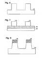
- a photoresist, or hardmask, such as CVD deposited SiO 2 , patternis fabricated, by any state-of-the art method, 22 . It is important that the sidewalls of the photoresist or hardmask are parallel to the silicon ( 111 ) or equivalent plane, as shown in FIG. 4 , wherein a silicon ( 110 ) substrate 24 has a mask 26 thereon. The mask sidewalls are parallel to the silicon ( 111 ) plane.
- FIG. 5depicts a SOI ( 110 ) wafer 28 , having a silicon substrate 30 , a BOX layer 32 thereon, and a top silicon ( 110 ) layer 34 . Mask elements 26 are formed on top silicon layer 24 , again so that the mask sidewalls are parallel to the silicon ( 111 ). Vertical silicon surfaces with silicon ( 111 ) sidewalls can then be fabricated by one of two methods:
- a selective chemistrysuch as a 2.38% tetramethylammonium hydroxide (TMAH) solution, is used to etch the ( 110 ) planes while barely etching the ( 111 ) planes, 36 , to remove a portion of the un-masked silicon ( 110 ) layer. The mask is then removed.
- This solutionetches silicon ( 110 ) about 23-25 times faster than it does silicon ( 111 ), which results in a sidewall slope of ⁇ 4% from vertical, or a 86° sidewall, as shown in FIGS. 6 and 7 .
- the height of the sidewallis determined by the etch time for the bulk silicon ( 110 ) wafer, FIG. 6 .
- SOISOI
- the advantage of this methodis that there is little or no damage to the crystal lattice along the sidewall surface.
- the disadvantageis that the sidewall angle is directly limited by etch selectivity, i.e., the higher the selectivity, the more vertical the sidewall.
- RIEmay be used to anisotropically etch 38 most of the un-masked silicon ( 110 ) layer, FIGS. 8 and 9 . Then, with the photoresist or hardmask pattern still intact, a short selective wet etch may be used to etch ( 110 ) while barely etching ( 111 ), as shown in FIGS. 10 and 11 . The mask is then removed.
- the advantage of this methodis that a more vertical sidewall results, i.e., closer to 90°.
- the disadvantageis that crystal damage near the sidewall needs to be removed. This may be done by several techniques, such as growing a thin thermal oxide and removing it with an HF etch, and/or annealing the etched silicon substrate to recrystallize the damaged region.
- the height of the resulting sidewallmay be adjusted to meet the needs of the application.
- sidewalls with heights of 0.1 micron to 1.0 micron, or morecan be fabricated.
- Strained SiGe films or strained SiGe/Si multilayer structures having a germanium content from 5% to 100%can then be epitaxially grown, 40 , on these patterned, remaining silicon ( 110 ) structures and used in photodetector fabrication, 42 , as described in by Lee et al., supra, for non-selective epitaxy, and by Tweet et al., supra, for selective epitaxy, i.e., epitaxial growth on silicon but not on oxide or nitride.
Landscapes
- Light Receiving Elements (AREA)
Abstract
Description
- This invention relates to photodetectors, and particularly to near-infrared photodetectors integrated on silicon substrates.
- Photo detecting in the near infrared regime, i.e., having a wavelength of between 0.7 μm to 2 μm, has many applications, such as in fiber-optic communication, security applications, machine vision and night vision imaging. Although III-V compound semiconductors provide superior optical performance over their silicon-based counterparts, the compatibility of silicon based materials with current silicon-IC technology provides the possibility of making cheap, small and highly integrated optical systems. The following references provide additional background for the invention: Maiti et al., Strained Silicon Heterostructures: Materials and Devices, Chapter 10: Si/SiGe Optoelectronics, The Institution of Electrical Engineer, 2001; Murtaza et al., Room Temperature Electroabsorption in GexSi1-xPIN Photodiode, IEEE Trans. on Electron Devices, 2297-2300, Vol. 41, No. 12, 1994; Tashiro et al., A Selective Epitaxial SiGe/Si Planar Photodetector for Si-Based OEICs, IEEE Trans. on Electron Devices, 545-550, Vol. 44, No. 4, 1997; Vonsovici et al., Room Temperature Photocurrent Spectroscopy of SiGe/Si p-i-n Photodiodes Grown by Selective Epitaxy, IEEE Trans. on Electron Devices, 538-542, Vol. 45, No. 2, 1998; and Jones et al., Fabrication and Modeling of Gigahertz Photodetectors in Heteroepitaxial Ge-on-Si using Graded Buffer Layer Deposited by Low Energy Plasma Enhanced CVD, IEDM, 2002.
- Silicon photodiodes are widely used as photodetectors for visible light due to their low dark current and compatibility with silicon IC technologies. The use of Si1-xGex(SiGe) alloys in silicon processing permits photo detection operating in the 0.8 μm to 1.6 μm wavelength regime.
- SiGe alloys have larger lattice constants than pure silicon, thus, the epitaxial growth of SiGe on silicon has a critical thickness, above which the film begins to relax by the nucleation of dislocations. The critical thickness of SiGe depends on the germanium concentration and device process temperature. Houghton, Strain relaxation kinetics in Si1-xGex/Si heterostructures, J. Appl. Phys. Vol. 780, No. 4, 1991.
- A high germanium concentration and high device process temperature result in a smaller critical thickness. In common practice, the SiGe critical thickness is in the range of few hundred angstroms to a maximum of a couple thousand angstroms. Once the SiGe thickness is grown above its critical thickness, lattice defects in SiGe are inevitable. An IR photo detector built on SiGe containing lattice defects will have a high dark current and produce electronic noise.
- Quantum efficiency is the number of electron-hole pairs generated per incident photon and is a parameter for photo detector sensitivity. The quantum efficiency is defined as:
η=(Ip/q)/(Popt/hν) (1)
where Ip is the photo-generated current by the absorption of incident optical power Poptat the light frequency ν, where q is the electron charge, and h is Planck's constant. - One of the key factors that determines the quantum efficiency is the absorption coefficient, α. Silicon has a cutoff wavelength of about 1.1 μm and is transparent to wavelengths beyond ˜1.2 μm. The SiGe absorption edge shifts to the red with increasing germanium mole fraction and is shown in
FIG. 1 . The absorption coefficient of SiGe alloy is small and the critical thickness limits the absorbing layer thickness. The major aim of SiGe based photo detectors is to achieve high quantum efficiency and integration with existing silicon electronics. - One way to increase the optical path and improve the quantum efficiency is to illuminate the edge of the photo detector with light so that the light propagates parallel to the heterojunction (SiGe/Si) interfaces. However, this does not allow the device to be used in image detection. Growing strained, defect-free SiGe films or SiGe/Si multilayer structures on the sidewalls of etched silicon structures has been disclosed by Lee et al., Surface-Normal Optical Path Structure for Infrared Photodetection, U.S. Patent Publication No. 2005/0136637-A1, published Jun. 23, 2005; and Tweet et al., Vertical Optical Path Structure for Infrared Photodetection, U.S. Patent Publication No. 2005/0153474-A1, published Jul. 14, 2005. In devices incorporating the technology described in the two preceding references, illumination of the device is normal to the silicon substrate, however, light travels parallel to the heterojunction interface to increase the optical path length. Therefore, two-dimensional IR image detection may be achieved within thin SiGe or SiGe/Si film thicknesses.
- Fabrication of high quality, defect-free strained SiGe films requires SiGe growth on a defect-free silicon surface. However, referring to
FIG. 2 , reactive ion-etching (RIE) of silicon usually results in a sloped sidewall, shown generally at10, and in poor crystal quality near the sidewall surface, as shown generally at12, where a damaged area of silicon is formed near an RIE-etched sidewall. Also, the surface is often rather rough. Ideally, these defects may be cured by use of a selective etch, which etches the desired sidewall crystal plane more slowly than it does other planes. For various kinds of silicon device fabrication, silicon substrates having a (001) plane parallel to the wafer surface are most commonly used. Etching of a trench in this substrate renders the sidewalls parallel to the (110) planes or (100) planes, depending on the azimuthal rotation of the wafer. Making these sidewalls more vertical requires a selective etch, which etches the (110) or (100) planes, respectively, more slowly than other planes. However, such an etch process is not known in the prior art. Instead, there are well-known selective etches which etch the (111) plane much more slowly than other planes. - One way around this problem is to change the substrate to one with the silicon (110) plane parallel to the wafer surface, Liu et al., Multi-Fin Double-Gate MOSFET Fabricated by using (110)-Oriented SOI wafers and Orientation-Dependent Etching, Electrochemical Society Proceedings, vol. 2003-06, 566 (2003). Then, the sidewall plane may be silicon (111) or any other related, equivalent orthogonal plane. Liu et al. used a 2.38% tetramethylammonium hydroxide (TMAH) solution to etch vertical sidewalls and form a silicon fin structure with rectangular cross-section on silicon-on-insulator wafers. These were then used to fabricate silicon-FINFET (FIN Field-Effect Transistor) devices. Liu et al. report that TMAH etches (110) planes 23-25 times faster than silicon (111) planes. In addition, the use of a selective wet etch instead of RIE results in undamaged crystalline silicon at the sidewall surfaces.
- A method of fabricating vertical sidewalls on silicon (110) substrates for use in Si/SiGe photodetectors includes preparing a silicon (110) layer wherein the silicon (110) plane is parallel to an underlying silicon wafer surface. Masking the silicon (110) layer with mask sidewalls parallel to a silicon (111) layer plane and etching the silicon (110) layer to remove an un-masked portion thereof, leaving a patterned silicon (110) layer. Finally, the mask is removed, and SiGe-containing layers are grown on the patterned silicon (110) layer. The photodetector is then completed.
- It is an object of the invention to improve the quantum efficiency of photodetectors, e.g., near-IR photodetectors, integrated on silicon substrates.
- Another object of the invention is to provide a method for using silicon (110) substrates and selective chemical etching to fabricate vertical sidewalls on which to grow strained SiGe and/or SiGe/Si multilayer structures for use in photodetectors, such as near-IR photodetectors.
- This summary and objectives of the invention are provided to enable quick comprehension of the nature of the invention. A more thorough understanding of the invention may be obtained by reference to the following detailed description of the preferred embodiment of the invention in connection with the drawings.
FIG. 1 represents normalized photocurrent spectra for various SiGe sample.FIG. 2 is a schematic profile of RIE-etched silicon structures.FIG. 3 is a block diagram of the method of the invention.FIG. 4 depicts use of a bulk silicon (110) substrate.FIG. 5 depicts use of a SOI (110) substrate.FIG. 6 depicts bulk silicon (110) substrate following direct use of selective wet etch.FIG. 7 depicts SOI (110) substrate following selective wet etch.FIG. 8 depicts bulk silicon (110) substrate following anisotropic RIE etch.FIG. 9 depicts SOI (110) substrate following anisotropic RIE etch.FIG. 10 depicts bulk silicon (110) substrate following anisotropic RIE etch and selective wet etch.FIG. 11 depicts SOI (110) substrate following anisotropic RIE etch and selective wet etch.- The objective of this invention is to improve the quantum efficiency of photodetectors, e.g., near-IR photodetectors, integrated on silicon substrates. This is done by providing silicon structures with nearly vertical sidewalls and low crystalline defects to enable the growth of low-defect strained, epitaxial SiGe and/or SiGe/Si multilayers on the sidewalls. By so doing, the optical path length for absorption of light is be determined by the height of the sidewalls, and not by the SiGe film thickness. In this way the quantum efficiency of the photodetector is improved.
- As previously noted, the use of reactive ion-etching (RIE) to etch silicon structures results in rough, damaged sidewalls with unacceptably large slopes. The readily available selective etch processes do not improve this situation on silicon (001) substrates. The present invention uses silicon (110) substrates and selective chemical etching to fabricate vertical sidewalls on which to grow strained SiGe and/or SiGe/Si multilayer structures for use in photodetectors, such as near-IR photodetectors.
- Referring now to
FIG. 3 , the method of the invention is depicted generally at14, includes preparation of a substrate, usually in the form of a silicon wafer,16. The starting substrate has a silicon (110) plane parallel to the wafer surface. The substrate may be a bulk silicon (110)wafer 18, or it may be a silicon-on-insulator (SOI) wafer in which the top silicon has the (110) plane parallel to the wafer surface, referred to herein as a SOI(110)wafer 20. In the latter case, the top silicon needs to be sufficiently thick, e.g., 0.1 micron to 1.0 micron, or more, so as to result in a longer optical path length of the deposited SiGe film than can be achieved by the usual deposition on a planar substrate, i.e., the critical thickness. Note that it is only necessary for the top silicon to have the (110) plane parallel to the wafer surface. If a wafer-bonding technique, such as SmartCut® or Eltran®, is used, the silicon substrate beneath the buried-oxide (BOX) may have the usual (100) orientation. This procedure is likely less expensive than using a substrate of silicon (110). - In preparation for forming the vertical silicon surfaces, a photoresist, or hardmask, such as CVD deposited SiO2, pattern is fabricated, by any state-of-the art method,22. It is important that the sidewalls of the photoresist or hardmask are parallel to the silicon (111) or equivalent plane, as shown in
FIG. 4 , wherein a silicon (110)substrate 24 has amask 26 thereon. The mask sidewalls are parallel to the silicon (111) plane.FIG. 5 depicts a SOI (110)wafer 28, having asilicon substrate 30, aBOX layer 32 thereon, and a top silicon (110)layer 34.Mask elements 26 are formed ontop silicon layer 24, again so that the mask sidewalls are parallel to the silicon (111). Vertical silicon surfaces with silicon (111) sidewalls can then be fabricated by one of two methods: - Wet Etch Only
- A selective chemistry, such as a 2.38% tetramethylammonium hydroxide (TMAH) solution, is used to etch the (110) planes while barely etching the (111) planes,36, to remove a portion of the un-masked silicon (110) layer. The mask is then removed. This solution etches silicon (110) about 23-25 times faster than it does silicon (111), which results in a sidewall slope of ˜4% from vertical, or a 86° sidewall, as shown in
FIGS. 6 and 7 . The height of the sidewall is determined by the etch time for the bulk silicon (110) wafer,FIG. 6 . In the case of SOI (110),FIG. 7 , the etch stops at the BOX, so the sidewall height is determined by the thickness of the top silicon. The advantage of this method is that there is little or no damage to the crystal lattice along the sidewall surface. The disadvantage is that the sidewall angle is directly limited by etch selectivity, i.e., the higher the selectivity, the more vertical the sidewall. - Reactive Ion Etch (RIE) Followed by Selective Wet Etch
- RIE may be used to
anisotropically etch 38 most of the un-masked silicon (110) layer,FIGS. 8 and 9 . Then, with the photoresist or hardmask pattern still intact, a short selective wet etch may be used to etch (110) while barely etching (111), as shown inFIGS. 10 and 11 . The mask is then removed. The advantage of this method is that a more vertical sidewall results, i.e., closer to 90°. The disadvantage is that crystal damage near the sidewall needs to be removed. This may be done by several techniques, such as growing a thin thermal oxide and removing it with an HF etch, and/or annealing the etched silicon substrate to recrystallize the damaged region. - In either case, the height of the resulting sidewall may be adjusted to meet the needs of the application. In general, sidewalls with heights of 0.1 micron to 1.0 micron, or more, can be fabricated. Strained SiGe films or strained SiGe/Si multilayer structures having a germanium content from 5% to 100% can then be epitaxially grown,40, on these patterned, remaining silicon (110) structures and used in photodetector fabrication,42, as described in by Lee et al., supra, for non-selective epitaxy, and by Tweet et al., supra, for selective epitaxy, i.e., epitaxial growth on silicon but not on oxide or nitride.
- Thus, a method for fabrication of vertical sidewalls on (110) silicon substrates for use in Si/SiGe photodetectors has been disclosed. It will be appreciated that further variations and modifications thereof may be made within the scope of the invention as defined in the appended claims.
Claims (15)
Priority Applications (2)
| Application Number | Priority Date | Filing Date | Title |
|---|---|---|---|
| US11/416,985US7297564B1 (en) | 2006-05-02 | 2006-05-02 | Fabrication of vertical sidewalls on (110) silicon substrates for use in Si/SiGe photodetectors |
| JP2007111008AJP2007300095A (en) | 2006-05-02 | 2007-04-19 | Method for manufacturing vertical sidewalls on a (110) silicon substrate for Si / SiGe photodetectors |
Applications Claiming Priority (1)
| Application Number | Priority Date | Filing Date | Title |
|---|---|---|---|
| US11/416,985US7297564B1 (en) | 2006-05-02 | 2006-05-02 | Fabrication of vertical sidewalls on (110) silicon substrates for use in Si/SiGe photodetectors |
Publications (2)
| Publication Number | Publication Date |
|---|---|
| US20070259467A1true US20070259467A1 (en) | 2007-11-08 |
| US7297564B1 US7297564B1 (en) | 2007-11-20 |
Family
ID=38661684
Family Applications (1)
| Application Number | Title | Priority Date | Filing Date |
|---|---|---|---|
| US11/416,985ActiveUS7297564B1 (en) | 2006-05-02 | 2006-05-02 | Fabrication of vertical sidewalls on (110) silicon substrates for use in Si/SiGe photodetectors |
Country Status (2)
| Country | Link |
|---|---|
| US (1) | US7297564B1 (en) |
| JP (1) | JP2007300095A (en) |
Cited By (133)
| Publication number | Priority date | Publication date | Assignee | Title |
|---|---|---|---|---|
| US20100229929A1 (en)* | 2009-03-16 | 2010-09-16 | Acorn Technologies, Inc. | Strained-Enhanced Silicon Photon-To-Electron Conversion Devices |
| CN102376813A (en)* | 2010-08-24 | 2012-03-14 | 中国科学院微电子研究所 | Uncooled infrared detector and manufacturing method thereof |
| US9064808B2 (en) | 2011-07-25 | 2015-06-23 | Synopsys, Inc. | Integrated circuit devices having features with reduced edge curvature and methods for manufacturing the same |
| US20150214337A1 (en)* | 2014-01-27 | 2015-07-30 | Applied Materials, Inc. | Method of fin patterning |
| US20150249112A1 (en)* | 2014-03-03 | 2015-09-03 | Sandisk 3D Llc | Vertical Thin Film Transistors In Non-Volatile Storage Systems |
| US9152750B2 (en) | 2011-09-08 | 2015-10-06 | Synopsys, Inc. | Methods for manufacturing integrated circuit devices having features with reduced edge curvature |
| US9299538B2 (en) | 2014-03-20 | 2016-03-29 | Applied Materials, Inc. | Radial waveguide systems and methods for post-match control of microwaves |
| US9299537B2 (en) | 2014-03-20 | 2016-03-29 | Applied Materials, Inc. | Radial waveguide systems and methods for post-match control of microwaves |
| US9343272B1 (en) | 2015-01-08 | 2016-05-17 | Applied Materials, Inc. | Self-aligned process |
| US9349605B1 (en) | 2015-08-07 | 2016-05-24 | Applied Materials, Inc. | Oxide etch selectivity systems and methods |
| US9355922B2 (en) | 2014-10-14 | 2016-05-31 | Applied Materials, Inc. | Systems and methods for internal surface conditioning in plasma processing equipment |
| US9355863B2 (en) | 2012-12-18 | 2016-05-31 | Applied Materials, Inc. | Non-local plasma oxide etch |
| US9355862B2 (en) | 2014-09-24 | 2016-05-31 | Applied Materials, Inc. | Fluorine-based hardmask removal |
| US9355856B2 (en) | 2014-09-12 | 2016-05-31 | Applied Materials, Inc. | V trench dry etch |
| US9362130B2 (en) | 2013-03-01 | 2016-06-07 | Applied Materials, Inc. | Enhanced etching processes using remote plasma sources |
| US9368364B2 (en) | 2014-09-24 | 2016-06-14 | Applied Materials, Inc. | Silicon etch process with tunable selectivity to SiO2 and other materials |
| US9373517B2 (en) | 2012-08-02 | 2016-06-21 | Applied Materials, Inc. | Semiconductor processing with DC assisted RF power for improved control |
| US9373522B1 (en) | 2015-01-22 | 2016-06-21 | Applied Mateials, Inc. | Titanium nitride removal |
| US9378978B2 (en) | 2014-07-31 | 2016-06-28 | Applied Materials, Inc. | Integrated oxide recess and floating gate fin trimming |
| US9378969B2 (en) | 2014-06-19 | 2016-06-28 | Applied Materials, Inc. | Low temperature gas-phase carbon removal |
| US9384997B2 (en) | 2012-11-20 | 2016-07-05 | Applied Materials, Inc. | Dry-etch selectivity |
| US9385028B2 (en) | 2014-02-03 | 2016-07-05 | Applied Materials, Inc. | Air gap process |
| US9390937B2 (en) | 2012-09-20 | 2016-07-12 | Applied Materials, Inc. | Silicon-carbon-nitride selective etch |
| US9396989B2 (en) | 2014-01-27 | 2016-07-19 | Applied Materials, Inc. | Air gaps between copper lines |
| US9406523B2 (en) | 2014-06-19 | 2016-08-02 | Applied Materials, Inc. | Highly selective doped oxide removal method |
| US9412608B2 (en) | 2012-11-30 | 2016-08-09 | Applied Materials, Inc. | Dry-etch for selective tungsten removal |
| US9418858B2 (en) | 2011-10-07 | 2016-08-16 | Applied Materials, Inc. | Selective etch of silicon by way of metastable hydrogen termination |
| US9425058B2 (en) | 2014-07-24 | 2016-08-23 | Applied Materials, Inc. | Simplified litho-etch-litho-etch process |
| US9437451B2 (en) | 2012-09-18 | 2016-09-06 | Applied Materials, Inc. | Radical-component oxide etch |
| US9449846B2 (en) | 2015-01-28 | 2016-09-20 | Applied Materials, Inc. | Vertical gate separation |
| US9449845B2 (en) | 2012-12-21 | 2016-09-20 | Applied Materials, Inc. | Selective titanium nitride etching |
| US9472412B2 (en) | 2013-12-02 | 2016-10-18 | Applied Materials, Inc. | Procedure for etch rate consistency |
| US9478432B2 (en) | 2014-09-25 | 2016-10-25 | Applied Materials, Inc. | Silicon oxide selective removal |
| US9496167B2 (en) | 2014-07-31 | 2016-11-15 | Applied Materials, Inc. | Integrated bit-line airgap formation and gate stack post clean |
| US9493879B2 (en) | 2013-07-12 | 2016-11-15 | Applied Materials, Inc. | Selective sputtering for pattern transfer |
| US9499898B2 (en) | 2014-03-03 | 2016-11-22 | Applied Materials, Inc. | Layered thin film heater and method of fabrication |
| US9502258B2 (en) | 2014-12-23 | 2016-11-22 | Applied Materials, Inc. | Anisotropic gap etch |
| US9520303B2 (en) | 2013-11-12 | 2016-12-13 | Applied Materials, Inc. | Aluminum selective etch |
| US9553102B2 (en) | 2014-08-19 | 2017-01-24 | Applied Materials, Inc. | Tungsten separation |
| US9576809B2 (en) | 2013-11-04 | 2017-02-21 | Applied Materials, Inc. | Etch suppression with germanium |
| US9607856B2 (en) | 2013-03-05 | 2017-03-28 | Applied Materials, Inc. | Selective titanium nitride removal |
| US9659792B2 (en) | 2013-03-15 | 2017-05-23 | Applied Materials, Inc. | Processing systems and methods for halide scavenging |
| US9659753B2 (en) | 2014-08-07 | 2017-05-23 | Applied Materials, Inc. | Grooved insulator to reduce leakage current |
| US9691645B2 (en) | 2015-08-06 | 2017-06-27 | Applied Materials, Inc. | Bolted wafer chuck thermal management systems and methods for wafer processing systems |
| US9721789B1 (en) | 2016-10-04 | 2017-08-01 | Applied Materials, Inc. | Saving ion-damaged spacers |
| US9728437B2 (en) | 2015-02-03 | 2017-08-08 | Applied Materials, Inc. | High temperature chuck for plasma processing systems |
| US9741593B2 (en) | 2015-08-06 | 2017-08-22 | Applied Materials, Inc. | Thermal management systems and methods for wafer processing systems |
| US9754800B2 (en) | 2010-05-27 | 2017-09-05 | Applied Materials, Inc. | Selective etch for silicon films |
| US9768034B1 (en) | 2016-11-11 | 2017-09-19 | Applied Materials, Inc. | Removal methods for high aspect ratio structures |
| US9773648B2 (en) | 2013-08-30 | 2017-09-26 | Applied Materials, Inc. | Dual discharge modes operation for remote plasma |
| US9842744B2 (en) | 2011-03-14 | 2017-12-12 | Applied Materials, Inc. | Methods for etch of SiN films |
| US9865484B1 (en) | 2016-06-29 | 2018-01-09 | Applied Materials, Inc. | Selective etch using material modification and RF pulsing |
| US9881805B2 (en) | 2015-03-02 | 2018-01-30 | Applied Materials, Inc. | Silicon selective removal |
| US9885117B2 (en) | 2014-03-31 | 2018-02-06 | Applied Materials, Inc. | Conditioned semiconductor system parts |
| US9887096B2 (en) | 2012-09-17 | 2018-02-06 | Applied Materials, Inc. | Differential silicon oxide etch |
| US9934942B1 (en) | 2016-10-04 | 2018-04-03 | Applied Materials, Inc. | Chamber with flow-through source |
| US9947549B1 (en) | 2016-10-10 | 2018-04-17 | Applied Materials, Inc. | Cobalt-containing material removal |
| US9966240B2 (en) | 2014-10-14 | 2018-05-08 | Applied Materials, Inc. | Systems and methods for internal surface conditioning assessment in plasma processing equipment |
| US9978564B2 (en) | 2012-09-21 | 2018-05-22 | Applied Materials, Inc. | Chemical control features in wafer process equipment |
| US10026621B2 (en) | 2016-11-14 | 2018-07-17 | Applied Materials, Inc. | SiN spacer profile patterning |
| US10043684B1 (en) | 2017-02-06 | 2018-08-07 | Applied Materials, Inc. | Self-limiting atomic thermal etching systems and methods |
| US10043674B1 (en) | 2017-08-04 | 2018-08-07 | Applied Materials, Inc. | Germanium etching systems and methods |
| US10049891B1 (en) | 2017-05-31 | 2018-08-14 | Applied Materials, Inc. | Selective in situ cobalt residue removal |
| US20180240713A1 (en)* | 2017-02-17 | 2018-08-23 | International Business Machines Corporation | Dual channel finfets having uniform fin heights |
| US10062585B2 (en) | 2016-10-04 | 2018-08-28 | Applied Materials, Inc. | Oxygen compatible plasma source |
| US10062579B2 (en) | 2016-10-07 | 2018-08-28 | Applied Materials, Inc. | Selective SiN lateral recess |
| US10062587B2 (en) | 2012-07-18 | 2018-08-28 | Applied Materials, Inc. | Pedestal with multi-zone temperature control and multiple purge capabilities |
| US10062575B2 (en) | 2016-09-09 | 2018-08-28 | Applied Materials, Inc. | Poly directional etch by oxidation |
| US10062578B2 (en) | 2011-03-14 | 2018-08-28 | Applied Materials, Inc. | Methods for etch of metal and metal-oxide films |
| US10128086B1 (en) | 2017-10-24 | 2018-11-13 | Applied Materials, Inc. | Silicon pretreatment for nitride removal |
| US10163696B2 (en) | 2016-11-11 | 2018-12-25 | Applied Materials, Inc. | Selective cobalt removal for bottom up gapfill |
| US10170336B1 (en) | 2017-08-04 | 2019-01-01 | Applied Materials, Inc. | Methods for anisotropic control of selective silicon removal |
| US10224210B2 (en) | 2014-12-09 | 2019-03-05 | Applied Materials, Inc. | Plasma processing system with direct outlet toroidal plasma source |
| US10242908B2 (en) | 2016-11-14 | 2019-03-26 | Applied Materials, Inc. | Airgap formation with damage-free copper |
| US10256079B2 (en) | 2013-02-08 | 2019-04-09 | Applied Materials, Inc. | Semiconductor processing systems having multiple plasma configurations |
| US10256112B1 (en) | 2017-12-08 | 2019-04-09 | Applied Materials, Inc. | Selective tungsten removal |
| US10283324B1 (en) | 2017-10-24 | 2019-05-07 | Applied Materials, Inc. | Oxygen treatment for nitride etching |
| US10283321B2 (en) | 2011-01-18 | 2019-05-07 | Applied Materials, Inc. | Semiconductor processing system and methods using capacitively coupled plasma |
| US10297458B2 (en) | 2017-08-07 | 2019-05-21 | Applied Materials, Inc. | Process window widening using coated parts in plasma etch processes |
| US10319600B1 (en) | 2018-03-12 | 2019-06-11 | Applied Materials, Inc. | Thermal silicon etch |
| US10319649B2 (en) | 2017-04-11 | 2019-06-11 | Applied Materials, Inc. | Optical emission spectroscopy (OES) for remote plasma monitoring |
| US10319739B2 (en) | 2017-02-08 | 2019-06-11 | Applied Materials, Inc. | Accommodating imperfectly aligned memory holes |
| US10354889B2 (en) | 2017-07-17 | 2019-07-16 | Applied Materials, Inc. | Non-halogen etching of silicon-containing materials |
| US10403507B2 (en) | 2017-02-03 | 2019-09-03 | Applied Materials, Inc. | Shaped etch profile with oxidation |
| US10431429B2 (en) | 2017-02-03 | 2019-10-01 | Applied Materials, Inc. | Systems and methods for radial and azimuthal control of plasma uniformity |
| US10468267B2 (en) | 2017-05-31 | 2019-11-05 | Applied Materials, Inc. | Water-free etching methods |
| US10465294B2 (en) | 2014-05-28 | 2019-11-05 | Applied Materials, Inc. | Oxide and metal removal |
| US10481404B1 (en)* | 2018-05-14 | 2019-11-19 | Palo Alto Research Center Incorporated | Rectangular cavity optical beam shaper and method of manufacturing the same |
| US10490406B2 (en) | 2018-04-10 | 2019-11-26 | Appled Materials, Inc. | Systems and methods for material breakthrough |
| US10497573B2 (en) | 2018-03-13 | 2019-12-03 | Applied Materials, Inc. | Selective atomic layer etching of semiconductor materials |
| US10504700B2 (en) | 2015-08-27 | 2019-12-10 | Applied Materials, Inc. | Plasma etching systems and methods with secondary plasma injection |
| US10504754B2 (en) | 2016-05-19 | 2019-12-10 | Applied Materials, Inc. | Systems and methods for improved semiconductor etching and component protection |
| US10522371B2 (en) | 2016-05-19 | 2019-12-31 | Applied Materials, Inc. | Systems and methods for improved semiconductor etching and component protection |
| US10541246B2 (en) | 2017-06-26 | 2020-01-21 | Applied Materials, Inc. | 3D flash memory cells which discourage cross-cell electrical tunneling |
| US10541184B2 (en) | 2017-07-11 | 2020-01-21 | Applied Materials, Inc. | Optical emission spectroscopic techniques for monitoring etching |
| US10546729B2 (en) | 2016-10-04 | 2020-01-28 | Applied Materials, Inc. | Dual-channel showerhead with improved profile |
| US10566206B2 (en) | 2016-12-27 | 2020-02-18 | Applied Materials, Inc. | Systems and methods for anisotropic material breakthrough |
| US10573496B2 (en) | 2014-12-09 | 2020-02-25 | Applied Materials, Inc. | Direct outlet toroidal plasma source |
| US10573527B2 (en) | 2018-04-06 | 2020-02-25 | Applied Materials, Inc. | Gas-phase selective etching systems and methods |
| US10593560B2 (en) | 2018-03-01 | 2020-03-17 | Applied Materials, Inc. | Magnetic induction plasma source for semiconductor processes and equipment |
| US10615047B2 (en) | 2018-02-28 | 2020-04-07 | Applied Materials, Inc. | Systems and methods to form airgaps |
| US10629473B2 (en) | 2016-09-09 | 2020-04-21 | Applied Materials, Inc. | Footing removal for nitride spacer |
| US10672642B2 (en) | 2018-07-24 | 2020-06-02 | Applied Materials, Inc. | Systems and methods for pedestal configuration |
| US10679870B2 (en) | 2018-02-15 | 2020-06-09 | Applied Materials, Inc. | Semiconductor processing chamber multistage mixing apparatus |
| US10699879B2 (en) | 2018-04-17 | 2020-06-30 | Applied Materials, Inc. | Two piece electrode assembly with gap for plasma control |
| US10727080B2 (en) | 2017-07-07 | 2020-07-28 | Applied Materials, Inc. | Tantalum-containing material removal |
| US10755941B2 (en) | 2018-07-06 | 2020-08-25 | Applied Materials, Inc. | Self-limiting selective etching systems and methods |
| US10854426B2 (en) | 2018-01-08 | 2020-12-01 | Applied Materials, Inc. | Metal recess for semiconductor structures |
| US10872778B2 (en) | 2018-07-06 | 2020-12-22 | Applied Materials, Inc. | Systems and methods utilizing solid-phase etchants |
| US10886137B2 (en) | 2018-04-30 | 2021-01-05 | Applied Materials, Inc. | Selective nitride removal |
| US10892198B2 (en) | 2018-09-14 | 2021-01-12 | Applied Materials, Inc. | Systems and methods for improved performance in semiconductor processing |
| US10903054B2 (en) | 2017-12-19 | 2021-01-26 | Applied Materials, Inc. | Multi-zone gas distribution systems and methods |
| US10920320B2 (en) | 2017-06-16 | 2021-02-16 | Applied Materials, Inc. | Plasma health determination in semiconductor substrate processing reactors |
| US10920319B2 (en) | 2019-01-11 | 2021-02-16 | Applied Materials, Inc. | Ceramic showerheads with conductive electrodes |
| US10943834B2 (en) | 2017-03-13 | 2021-03-09 | Applied Materials, Inc. | Replacement contact process |
| US10964512B2 (en) | 2018-02-15 | 2021-03-30 | Applied Materials, Inc. | Semiconductor processing chamber multistage mixing apparatus and methods |
| US11049755B2 (en) | 2018-09-14 | 2021-06-29 | Applied Materials, Inc. | Semiconductor substrate supports with embedded RF shield |
| US11062887B2 (en) | 2018-09-17 | 2021-07-13 | Applied Materials, Inc. | High temperature RF heater pedestals |
| US11121002B2 (en) | 2018-10-24 | 2021-09-14 | Applied Materials, Inc. | Systems and methods for etching metals and metal derivatives |
| US11139402B2 (en) | 2018-05-14 | 2021-10-05 | Synopsys, Inc. | Crystal orientation engineering to achieve consistent nanowire shapes |
| US11239061B2 (en) | 2014-11-26 | 2022-02-01 | Applied Materials, Inc. | Methods and systems to enhance process uniformity |
| US11257693B2 (en) | 2015-01-09 | 2022-02-22 | Applied Materials, Inc. | Methods and systems to improve pedestal temperature control |
| US11264458B2 (en) | 2019-05-20 | 2022-03-01 | Synopsys, Inc. | Crystal orientation engineering to achieve consistent nanowire shapes |
| US11276559B2 (en) | 2017-05-17 | 2022-03-15 | Applied Materials, Inc. | Semiconductor processing chamber for multiple precursor flow |
| US11276590B2 (en) | 2017-05-17 | 2022-03-15 | Applied Materials, Inc. | Multi-zone semiconductor substrate supports |
| US11328909B2 (en) | 2017-12-22 | 2022-05-10 | Applied Materials, Inc. | Chamber conditioning and removal processes |
| US11417534B2 (en) | 2018-09-21 | 2022-08-16 | Applied Materials, Inc. | Selective material removal |
| US11437242B2 (en) | 2018-11-27 | 2022-09-06 | Applied Materials, Inc. | Selective removal of silicon-containing materials |
| US11594428B2 (en) | 2015-02-03 | 2023-02-28 | Applied Materials, Inc. | Low temperature chuck for plasma processing systems |
| US11682560B2 (en) | 2018-10-11 | 2023-06-20 | Applied Materials, Inc. | Systems and methods for hafnium-containing film removal |
| US11721527B2 (en) | 2019-01-07 | 2023-08-08 | Applied Materials, Inc. | Processing chamber mixing systems |
| US11728624B2 (en) | 2011-08-12 | 2023-08-15 | Acorn Semi, Llc | Tensile strained semiconductor photon emission and detection devices and integrated photonics system |
| US12340979B2 (en) | 2017-05-17 | 2025-06-24 | Applied Materials, Inc. | Semiconductor processing chamber for improved precursor flow |
Families Citing this family (2)
| Publication number | Priority date | Publication date | Assignee | Title |
|---|---|---|---|---|
| JP6378928B2 (en)* | 2014-05-15 | 2018-08-22 | 富士通株式会社 | Ge-based semiconductor device, manufacturing method thereof, and optical interconnect system |
| US11677041B2 (en)* | 2014-06-23 | 2023-06-13 | Rensselaer Polytechnic Institute | Radiation-detecting structures and fabrication methods thereof |
Citations (5)
| Publication number | Priority date | Publication date | Assignee | Title |
|---|---|---|---|---|
| US5994724A (en)* | 1996-12-03 | 1999-11-30 | Nec Corporation | Photodetector |
| US6639249B2 (en)* | 2001-08-06 | 2003-10-28 | Motorola, Inc. | Structure and method for fabrication for a solid-state lighting device |
| US20050127275A1 (en)* | 2003-12-16 | 2005-06-16 | Min Yang | Photodetector with hetero-structure using lateral growth |
| US20050136637A1 (en)* | 2003-12-18 | 2005-06-23 | Sharp Laboratories Of America, Inc. | Indium oxide conductive film structures |
| US20050153474A1 (en)* | 2003-12-23 | 2005-07-14 | Sharp Laboratories Of America, Inc. | Vertical optical path structure for infrared photodetection |
- 2006
- 2006-05-02USUS11/416,985patent/US7297564B1/enactiveActive
- 2007
- 2007-04-19JPJP2007111008Apatent/JP2007300095A/enactivePending
Patent Citations (5)
| Publication number | Priority date | Publication date | Assignee | Title |
|---|---|---|---|---|
| US5994724A (en)* | 1996-12-03 | 1999-11-30 | Nec Corporation | Photodetector |
| US6639249B2 (en)* | 2001-08-06 | 2003-10-28 | Motorola, Inc. | Structure and method for fabrication for a solid-state lighting device |
| US20050127275A1 (en)* | 2003-12-16 | 2005-06-16 | Min Yang | Photodetector with hetero-structure using lateral growth |
| US20050136637A1 (en)* | 2003-12-18 | 2005-06-23 | Sharp Laboratories Of America, Inc. | Indium oxide conductive film structures |
| US20050153474A1 (en)* | 2003-12-23 | 2005-07-14 | Sharp Laboratories Of America, Inc. | Vertical optical path structure for infrared photodetection |
Cited By (194)
| Publication number | Priority date | Publication date | Assignee | Title |
|---|---|---|---|---|
| US20100229929A1 (en)* | 2009-03-16 | 2010-09-16 | Acorn Technologies, Inc. | Strained-Enhanced Silicon Photon-To-Electron Conversion Devices |
| WO2010107578A1 (en)* | 2009-03-16 | 2010-09-23 | Acorn Technologies, Inc. | Strain-enhanced silicon photon-to-electron conversion devices |
| US8450133B2 (en) | 2009-03-16 | 2013-05-28 | Acorn Technologies, Inc. | Strained-enhanced silicon photon-to-electron conversion devices |
| US9029686B2 (en)* | 2009-03-16 | 2015-05-12 | Acorn Technologies, Inc. | Strain-enhanced silicon photon-to-electron conversion devices |
| US9754800B2 (en) | 2010-05-27 | 2017-09-05 | Applied Materials, Inc. | Selective etch for silicon films |
| CN102376813A (en)* | 2010-08-24 | 2012-03-14 | 中国科学院微电子研究所 | Uncooled infrared detector and manufacturing method thereof |
| US10283321B2 (en) | 2011-01-18 | 2019-05-07 | Applied Materials, Inc. | Semiconductor processing system and methods using capacitively coupled plasma |
| US9842744B2 (en) | 2011-03-14 | 2017-12-12 | Applied Materials, Inc. | Methods for etch of SiN films |
| US10062578B2 (en) | 2011-03-14 | 2018-08-28 | Applied Materials, Inc. | Methods for etch of metal and metal-oxide films |
| US9064808B2 (en) | 2011-07-25 | 2015-06-23 | Synopsys, Inc. | Integrated circuit devices having features with reduced edge curvature and methods for manufacturing the same |
| US9786734B2 (en) | 2011-07-25 | 2017-10-10 | Synopsys, Inc. | Integrated circuit devices having features with reduced edge curvature and methods for manufacturing the same |
| US10256293B2 (en) | 2011-07-25 | 2019-04-09 | Synopsys, Inc. | Integrated circuit devices having features with reduced edge curvature and methods for manufacturing the same |
| US11728624B2 (en) | 2011-08-12 | 2023-08-15 | Acorn Semi, Llc | Tensile strained semiconductor photon emission and detection devices and integrated photonics system |
| US9152750B2 (en) | 2011-09-08 | 2015-10-06 | Synopsys, Inc. | Methods for manufacturing integrated circuit devices having features with reduced edge curvature |
| US10032859B2 (en) | 2011-09-08 | 2018-07-24 | Synopsys, Inc. | Methods for manufacturing integrated circuit devices having features with reduced edge curvature |
| US9379183B2 (en) | 2011-09-08 | 2016-06-28 | Synopsys, Inc. | Methods for manufacturing integrated circuit devices having features with reduced edge curvature |
| US9418858B2 (en) | 2011-10-07 | 2016-08-16 | Applied Materials, Inc. | Selective etch of silicon by way of metastable hydrogen termination |
| US10062587B2 (en) | 2012-07-18 | 2018-08-28 | Applied Materials, Inc. | Pedestal with multi-zone temperature control and multiple purge capabilities |
| US10032606B2 (en) | 2012-08-02 | 2018-07-24 | Applied Materials, Inc. | Semiconductor processing with DC assisted RF power for improved control |
| US9373517B2 (en) | 2012-08-02 | 2016-06-21 | Applied Materials, Inc. | Semiconductor processing with DC assisted RF power for improved control |
| US9887096B2 (en) | 2012-09-17 | 2018-02-06 | Applied Materials, Inc. | Differential silicon oxide etch |
| US9437451B2 (en) | 2012-09-18 | 2016-09-06 | Applied Materials, Inc. | Radical-component oxide etch |
| US9390937B2 (en) | 2012-09-20 | 2016-07-12 | Applied Materials, Inc. | Silicon-carbon-nitride selective etch |
| US11264213B2 (en) | 2012-09-21 | 2022-03-01 | Applied Materials, Inc. | Chemical control features in wafer process equipment |
| US10354843B2 (en) | 2012-09-21 | 2019-07-16 | Applied Materials, Inc. | Chemical control features in wafer process equipment |
| US9978564B2 (en) | 2012-09-21 | 2018-05-22 | Applied Materials, Inc. | Chemical control features in wafer process equipment |
| US9384997B2 (en) | 2012-11-20 | 2016-07-05 | Applied Materials, Inc. | Dry-etch selectivity |
| US9412608B2 (en) | 2012-11-30 | 2016-08-09 | Applied Materials, Inc. | Dry-etch for selective tungsten removal |
| US9355863B2 (en) | 2012-12-18 | 2016-05-31 | Applied Materials, Inc. | Non-local plasma oxide etch |
| US9449845B2 (en) | 2012-12-21 | 2016-09-20 | Applied Materials, Inc. | Selective titanium nitride etching |
| US11024486B2 (en) | 2013-02-08 | 2021-06-01 | Applied Materials, Inc. | Semiconductor processing systems having multiple plasma configurations |
| US10256079B2 (en) | 2013-02-08 | 2019-04-09 | Applied Materials, Inc. | Semiconductor processing systems having multiple plasma configurations |
| US10424485B2 (en) | 2013-03-01 | 2019-09-24 | Applied Materials, Inc. | Enhanced etching processes using remote plasma sources |
| US9362130B2 (en) | 2013-03-01 | 2016-06-07 | Applied Materials, Inc. | Enhanced etching processes using remote plasma sources |
| US9607856B2 (en) | 2013-03-05 | 2017-03-28 | Applied Materials, Inc. | Selective titanium nitride removal |
| US9704723B2 (en) | 2013-03-15 | 2017-07-11 | Applied Materials, Inc. | Processing systems and methods for halide scavenging |
| US9659792B2 (en) | 2013-03-15 | 2017-05-23 | Applied Materials, Inc. | Processing systems and methods for halide scavenging |
| US9493879B2 (en) | 2013-07-12 | 2016-11-15 | Applied Materials, Inc. | Selective sputtering for pattern transfer |
| US9773648B2 (en) | 2013-08-30 | 2017-09-26 | Applied Materials, Inc. | Dual discharge modes operation for remote plasma |
| US9576809B2 (en) | 2013-11-04 | 2017-02-21 | Applied Materials, Inc. | Etch suppression with germanium |
| US9711366B2 (en) | 2013-11-12 | 2017-07-18 | Applied Materials, Inc. | Selective etch for metal-containing materials |
| US9520303B2 (en) | 2013-11-12 | 2016-12-13 | Applied Materials, Inc. | Aluminum selective etch |
| US9472412B2 (en) | 2013-12-02 | 2016-10-18 | Applied Materials, Inc. | Procedure for etch rate consistency |
| US20150214337A1 (en)* | 2014-01-27 | 2015-07-30 | Applied Materials, Inc. | Method of fin patterning |
| US9293568B2 (en)* | 2014-01-27 | 2016-03-22 | Applied Materials, Inc. | Method of fin patterning |
| US9396989B2 (en) | 2014-01-27 | 2016-07-19 | Applied Materials, Inc. | Air gaps between copper lines |
| US9385028B2 (en) | 2014-02-03 | 2016-07-05 | Applied Materials, Inc. | Air gap process |
| US9818798B2 (en) | 2014-03-03 | 2017-11-14 | Sandisk Technologies Llc | Vertical thin film transistors in non-volatile storage systems |
| US9499898B2 (en) | 2014-03-03 | 2016-11-22 | Applied Materials, Inc. | Layered thin film heater and method of fabrication |
| US20150249112A1 (en)* | 2014-03-03 | 2015-09-03 | Sandisk 3D Llc | Vertical Thin Film Transistors In Non-Volatile Storage Systems |
| US9362338B2 (en)* | 2014-03-03 | 2016-06-07 | Sandisk Technologies Inc. | Vertical thin film transistors in non-volatile storage systems |
| US9299538B2 (en) | 2014-03-20 | 2016-03-29 | Applied Materials, Inc. | Radial waveguide systems and methods for post-match control of microwaves |
| US9564296B2 (en) | 2014-03-20 | 2017-02-07 | Applied Materials, Inc. | Radial waveguide systems and methods for post-match control of microwaves |
| US9837249B2 (en) | 2014-03-20 | 2017-12-05 | Applied Materials, Inc. | Radial waveguide systems and methods for post-match control of microwaves |
| US9299537B2 (en) | 2014-03-20 | 2016-03-29 | Applied Materials, Inc. | Radial waveguide systems and methods for post-match control of microwaves |
| US9903020B2 (en) | 2014-03-31 | 2018-02-27 | Applied Materials, Inc. | Generation of compact alumina passivation layers on aluminum plasma equipment components |
| US9885117B2 (en) | 2014-03-31 | 2018-02-06 | Applied Materials, Inc. | Conditioned semiconductor system parts |
| US10465294B2 (en) | 2014-05-28 | 2019-11-05 | Applied Materials, Inc. | Oxide and metal removal |
| US9378969B2 (en) | 2014-06-19 | 2016-06-28 | Applied Materials, Inc. | Low temperature gas-phase carbon removal |
| US9406523B2 (en) | 2014-06-19 | 2016-08-02 | Applied Materials, Inc. | Highly selective doped oxide removal method |
| US9425058B2 (en) | 2014-07-24 | 2016-08-23 | Applied Materials, Inc. | Simplified litho-etch-litho-etch process |
| US9496167B2 (en) | 2014-07-31 | 2016-11-15 | Applied Materials, Inc. | Integrated bit-line airgap formation and gate stack post clean |
| US9773695B2 (en) | 2014-07-31 | 2017-09-26 | Applied Materials, Inc. | Integrated bit-line airgap formation and gate stack post clean |
| US9378978B2 (en) | 2014-07-31 | 2016-06-28 | Applied Materials, Inc. | Integrated oxide recess and floating gate fin trimming |
| US9659753B2 (en) | 2014-08-07 | 2017-05-23 | Applied Materials, Inc. | Grooved insulator to reduce leakage current |
| US9553102B2 (en) | 2014-08-19 | 2017-01-24 | Applied Materials, Inc. | Tungsten separation |
| US9355856B2 (en) | 2014-09-12 | 2016-05-31 | Applied Materials, Inc. | V trench dry etch |
| US9355862B2 (en) | 2014-09-24 | 2016-05-31 | Applied Materials, Inc. | Fluorine-based hardmask removal |
| US9478434B2 (en) | 2014-09-24 | 2016-10-25 | Applied Materials, Inc. | Chlorine-based hardmask removal |
| US9368364B2 (en) | 2014-09-24 | 2016-06-14 | Applied Materials, Inc. | Silicon etch process with tunable selectivity to SiO2 and other materials |
| US9613822B2 (en) | 2014-09-25 | 2017-04-04 | Applied Materials, Inc. | Oxide etch selectivity enhancement |
| US9478432B2 (en) | 2014-09-25 | 2016-10-25 | Applied Materials, Inc. | Silicon oxide selective removal |
| US9837284B2 (en) | 2014-09-25 | 2017-12-05 | Applied Materials, Inc. | Oxide etch selectivity enhancement |
| US10796922B2 (en) | 2014-10-14 | 2020-10-06 | Applied Materials, Inc. | Systems and methods for internal surface conditioning assessment in plasma processing equipment |
| US10593523B2 (en) | 2014-10-14 | 2020-03-17 | Applied Materials, Inc. | Systems and methods for internal surface conditioning in plasma processing equipment |
| US9355922B2 (en) | 2014-10-14 | 2016-05-31 | Applied Materials, Inc. | Systems and methods for internal surface conditioning in plasma processing equipment |
| US10490418B2 (en) | 2014-10-14 | 2019-11-26 | Applied Materials, Inc. | Systems and methods for internal surface conditioning assessment in plasma processing equipment |
| US9966240B2 (en) | 2014-10-14 | 2018-05-08 | Applied Materials, Inc. | Systems and methods for internal surface conditioning assessment in plasma processing equipment |
| US10707061B2 (en) | 2014-10-14 | 2020-07-07 | Applied Materials, Inc. | Systems and methods for internal surface conditioning in plasma processing equipment |
| US11239061B2 (en) | 2014-11-26 | 2022-02-01 | Applied Materials, Inc. | Methods and systems to enhance process uniformity |
| US11637002B2 (en) | 2014-11-26 | 2023-04-25 | Applied Materials, Inc. | Methods and systems to enhance process uniformity |
| US10573496B2 (en) | 2014-12-09 | 2020-02-25 | Applied Materials, Inc. | Direct outlet toroidal plasma source |
| US10224210B2 (en) | 2014-12-09 | 2019-03-05 | Applied Materials, Inc. | Plasma processing system with direct outlet toroidal plasma source |
| US9502258B2 (en) | 2014-12-23 | 2016-11-22 | Applied Materials, Inc. | Anisotropic gap etch |
| US9343272B1 (en) | 2015-01-08 | 2016-05-17 | Applied Materials, Inc. | Self-aligned process |
| US11257693B2 (en) | 2015-01-09 | 2022-02-22 | Applied Materials, Inc. | Methods and systems to improve pedestal temperature control |
| US9373522B1 (en) | 2015-01-22 | 2016-06-21 | Applied Mateials, Inc. | Titanium nitride removal |
| US9449846B2 (en) | 2015-01-28 | 2016-09-20 | Applied Materials, Inc. | Vertical gate separation |
| US12009228B2 (en) | 2015-02-03 | 2024-06-11 | Applied Materials, Inc. | Low temperature chuck for plasma processing systems |
| US10468285B2 (en) | 2015-02-03 | 2019-11-05 | Applied Materials, Inc. | High temperature chuck for plasma processing systems |
| US9728437B2 (en) | 2015-02-03 | 2017-08-08 | Applied Materials, Inc. | High temperature chuck for plasma processing systems |
| US11594428B2 (en) | 2015-02-03 | 2023-02-28 | Applied Materials, Inc. | Low temperature chuck for plasma processing systems |
| US9881805B2 (en) | 2015-03-02 | 2018-01-30 | Applied Materials, Inc. | Silicon selective removal |
| US10468276B2 (en) | 2015-08-06 | 2019-11-05 | Applied Materials, Inc. | Thermal management systems and methods for wafer processing systems |
| US10607867B2 (en) | 2015-08-06 | 2020-03-31 | Applied Materials, Inc. | Bolted wafer chuck thermal management systems and methods for wafer processing systems |
| US9691645B2 (en) | 2015-08-06 | 2017-06-27 | Applied Materials, Inc. | Bolted wafer chuck thermal management systems and methods for wafer processing systems |
| US9741593B2 (en) | 2015-08-06 | 2017-08-22 | Applied Materials, Inc. | Thermal management systems and methods for wafer processing systems |
| US10147620B2 (en) | 2015-08-06 | 2018-12-04 | Applied Materials, Inc. | Bolted wafer chuck thermal management systems and methods for wafer processing systems |
| US11158527B2 (en) | 2015-08-06 | 2021-10-26 | Applied Materials, Inc. | Thermal management systems and methods for wafer processing systems |
| US10424464B2 (en) | 2015-08-07 | 2019-09-24 | Applied Materials, Inc. | Oxide etch selectivity systems and methods |
| US9349605B1 (en) | 2015-08-07 | 2016-05-24 | Applied Materials, Inc. | Oxide etch selectivity systems and methods |
| US10424463B2 (en) | 2015-08-07 | 2019-09-24 | Applied Materials, Inc. | Oxide etch selectivity systems and methods |
| US10504700B2 (en) | 2015-08-27 | 2019-12-10 | Applied Materials, Inc. | Plasma etching systems and methods with secondary plasma injection |
| US11476093B2 (en) | 2015-08-27 | 2022-10-18 | Applied Materials, Inc. | Plasma etching systems and methods with secondary plasma injection |
| US10504754B2 (en) | 2016-05-19 | 2019-12-10 | Applied Materials, Inc. | Systems and methods for improved semiconductor etching and component protection |
| US10522371B2 (en) | 2016-05-19 | 2019-12-31 | Applied Materials, Inc. | Systems and methods for improved semiconductor etching and component protection |
| US11735441B2 (en) | 2016-05-19 | 2023-08-22 | Applied Materials, Inc. | Systems and methods for improved semiconductor etching and component protection |
| US9865484B1 (en) | 2016-06-29 | 2018-01-09 | Applied Materials, Inc. | Selective etch using material modification and RF pulsing |
| US12057329B2 (en) | 2016-06-29 | 2024-08-06 | Applied Materials, Inc. | Selective etch using material modification and RF pulsing |
| US10629473B2 (en) | 2016-09-09 | 2020-04-21 | Applied Materials, Inc. | Footing removal for nitride spacer |
| US10062575B2 (en) | 2016-09-09 | 2018-08-28 | Applied Materials, Inc. | Poly directional etch by oxidation |
| US10224180B2 (en) | 2016-10-04 | 2019-03-05 | Applied Materials, Inc. | Chamber with flow-through source |
| US9934942B1 (en) | 2016-10-04 | 2018-04-03 | Applied Materials, Inc. | Chamber with flow-through source |
| US10546729B2 (en) | 2016-10-04 | 2020-01-28 | Applied Materials, Inc. | Dual-channel showerhead with improved profile |
| US11049698B2 (en) | 2016-10-04 | 2021-06-29 | Applied Materials, Inc. | Dual-channel showerhead with improved profile |
| US10541113B2 (en) | 2016-10-04 | 2020-01-21 | Applied Materials, Inc. | Chamber with flow-through source |
| US9721789B1 (en) | 2016-10-04 | 2017-08-01 | Applied Materials, Inc. | Saving ion-damaged spacers |
| US10062585B2 (en) | 2016-10-04 | 2018-08-28 | Applied Materials, Inc. | Oxygen compatible plasma source |
| US10062579B2 (en) | 2016-10-07 | 2018-08-28 | Applied Materials, Inc. | Selective SiN lateral recess |
| US10319603B2 (en) | 2016-10-07 | 2019-06-11 | Applied Materials, Inc. | Selective SiN lateral recess |
| US9947549B1 (en) | 2016-10-10 | 2018-04-17 | Applied Materials, Inc. | Cobalt-containing material removal |
| US10163696B2 (en) | 2016-11-11 | 2018-12-25 | Applied Materials, Inc. | Selective cobalt removal for bottom up gapfill |
| US10770346B2 (en) | 2016-11-11 | 2020-09-08 | Applied Materials, Inc. | Selective cobalt removal for bottom up gapfill |
| US10186428B2 (en) | 2016-11-11 | 2019-01-22 | Applied Materials, Inc. | Removal methods for high aspect ratio structures |
| US9768034B1 (en) | 2016-11-11 | 2017-09-19 | Applied Materials, Inc. | Removal methods for high aspect ratio structures |
| US10026621B2 (en) | 2016-11-14 | 2018-07-17 | Applied Materials, Inc. | SiN spacer profile patterning |
| US10600639B2 (en) | 2016-11-14 | 2020-03-24 | Applied Materials, Inc. | SiN spacer profile patterning |
| US10242908B2 (en) | 2016-11-14 | 2019-03-26 | Applied Materials, Inc. | Airgap formation with damage-free copper |
| US10566206B2 (en) | 2016-12-27 | 2020-02-18 | Applied Materials, Inc. | Systems and methods for anisotropic material breakthrough |
| US10903052B2 (en) | 2017-02-03 | 2021-01-26 | Applied Materials, Inc. | Systems and methods for radial and azimuthal control of plasma uniformity |
| US10431429B2 (en) | 2017-02-03 | 2019-10-01 | Applied Materials, Inc. | Systems and methods for radial and azimuthal control of plasma uniformity |
| US10403507B2 (en) | 2017-02-03 | 2019-09-03 | Applied Materials, Inc. | Shaped etch profile with oxidation |
| US10043684B1 (en) | 2017-02-06 | 2018-08-07 | Applied Materials, Inc. | Self-limiting atomic thermal etching systems and methods |
| US10529737B2 (en) | 2017-02-08 | 2020-01-07 | Applied Materials, Inc. | Accommodating imperfectly aligned memory holes |
| US10325923B2 (en) | 2017-02-08 | 2019-06-18 | Applied Materials, Inc. | Accommodating imperfectly aligned memory holes |
| US10319739B2 (en) | 2017-02-08 | 2019-06-11 | Applied Materials, Inc. | Accommodating imperfectly aligned memory holes |
| US20180240713A1 (en)* | 2017-02-17 | 2018-08-23 | International Business Machines Corporation | Dual channel finfets having uniform fin heights |
| US10546788B2 (en) | 2017-02-17 | 2020-01-28 | International Business Machines Corporation | Dual channel FinFETs having uniform fin heights |
| US10438855B2 (en)* | 2017-02-17 | 2019-10-08 | International Business Machines Corporation | Dual channel FinFETs having uniform fin heights |
| US10943834B2 (en) | 2017-03-13 | 2021-03-09 | Applied Materials, Inc. | Replacement contact process |
| US10319649B2 (en) | 2017-04-11 | 2019-06-11 | Applied Materials, Inc. | Optical emission spectroscopy (OES) for remote plasma monitoring |
| US12340979B2 (en) | 2017-05-17 | 2025-06-24 | Applied Materials, Inc. | Semiconductor processing chamber for improved precursor flow |
| US11276559B2 (en) | 2017-05-17 | 2022-03-15 | Applied Materials, Inc. | Semiconductor processing chamber for multiple precursor flow |
| US11361939B2 (en) | 2017-05-17 | 2022-06-14 | Applied Materials, Inc. | Semiconductor processing chamber for multiple precursor flow |
| US11276590B2 (en) | 2017-05-17 | 2022-03-15 | Applied Materials, Inc. | Multi-zone semiconductor substrate supports |
| US11915950B2 (en) | 2017-05-17 | 2024-02-27 | Applied Materials, Inc. | Multi-zone semiconductor substrate supports |
| US10497579B2 (en) | 2017-05-31 | 2019-12-03 | Applied Materials, Inc. | Water-free etching methods |
| US10049891B1 (en) | 2017-05-31 | 2018-08-14 | Applied Materials, Inc. | Selective in situ cobalt residue removal |
| US10468267B2 (en) | 2017-05-31 | 2019-11-05 | Applied Materials, Inc. | Water-free etching methods |
| US10920320B2 (en) | 2017-06-16 | 2021-02-16 | Applied Materials, Inc. | Plasma health determination in semiconductor substrate processing reactors |
| US10541246B2 (en) | 2017-06-26 | 2020-01-21 | Applied Materials, Inc. | 3D flash memory cells which discourage cross-cell electrical tunneling |
| US10727080B2 (en) | 2017-07-07 | 2020-07-28 | Applied Materials, Inc. | Tantalum-containing material removal |
| US10541184B2 (en) | 2017-07-11 | 2020-01-21 | Applied Materials, Inc. | Optical emission spectroscopic techniques for monitoring etching |
| US10354889B2 (en) | 2017-07-17 | 2019-07-16 | Applied Materials, Inc. | Non-halogen etching of silicon-containing materials |
| US10170336B1 (en) | 2017-08-04 | 2019-01-01 | Applied Materials, Inc. | Methods for anisotropic control of selective silicon removal |
| US10043674B1 (en) | 2017-08-04 | 2018-08-07 | Applied Materials, Inc. | Germanium etching systems and methods |
| US10593553B2 (en) | 2017-08-04 | 2020-03-17 | Applied Materials, Inc. | Germanium etching systems and methods |
| US10297458B2 (en) | 2017-08-07 | 2019-05-21 | Applied Materials, Inc. | Process window widening using coated parts in plasma etch processes |
| US11101136B2 (en) | 2017-08-07 | 2021-08-24 | Applied Materials, Inc. | Process window widening using coated parts in plasma etch processes |
| US10283324B1 (en) | 2017-10-24 | 2019-05-07 | Applied Materials, Inc. | Oxygen treatment for nitride etching |
| US10128086B1 (en) | 2017-10-24 | 2018-11-13 | Applied Materials, Inc. | Silicon pretreatment for nitride removal |
| US10256112B1 (en) | 2017-12-08 | 2019-04-09 | Applied Materials, Inc. | Selective tungsten removal |
| US12148597B2 (en) | 2017-12-19 | 2024-11-19 | Applied Materials, Inc. | Multi-zone gas distribution systems and methods |
| US10903054B2 (en) | 2017-12-19 | 2021-01-26 | Applied Materials, Inc. | Multi-zone gas distribution systems and methods |
| US11328909B2 (en) | 2017-12-22 | 2022-05-10 | Applied Materials, Inc. | Chamber conditioning and removal processes |
| US10861676B2 (en) | 2018-01-08 | 2020-12-08 | Applied Materials, Inc. | Metal recess for semiconductor structures |
| US10854426B2 (en) | 2018-01-08 | 2020-12-01 | Applied Materials, Inc. | Metal recess for semiconductor structures |
| US10964512B2 (en) | 2018-02-15 | 2021-03-30 | Applied Materials, Inc. | Semiconductor processing chamber multistage mixing apparatus and methods |
| US10679870B2 (en) | 2018-02-15 | 2020-06-09 | Applied Materials, Inc. | Semiconductor processing chamber multistage mixing apparatus |
| US10699921B2 (en) | 2018-02-15 | 2020-06-30 | Applied Materials, Inc. | Semiconductor processing chamber multistage mixing apparatus |
| US10615047B2 (en) | 2018-02-28 | 2020-04-07 | Applied Materials, Inc. | Systems and methods to form airgaps |
| US10593560B2 (en) | 2018-03-01 | 2020-03-17 | Applied Materials, Inc. | Magnetic induction plasma source for semiconductor processes and equipment |
| US11004689B2 (en) | 2018-03-12 | 2021-05-11 | Applied Materials, Inc. | Thermal silicon etch |
| US10319600B1 (en) | 2018-03-12 | 2019-06-11 | Applied Materials, Inc. | Thermal silicon etch |
| US10497573B2 (en) | 2018-03-13 | 2019-12-03 | Applied Materials, Inc. | Selective atomic layer etching of semiconductor materials |
| US10573527B2 (en) | 2018-04-06 | 2020-02-25 | Applied Materials, Inc. | Gas-phase selective etching systems and methods |
| US10490406B2 (en) | 2018-04-10 | 2019-11-26 | Appled Materials, Inc. | Systems and methods for material breakthrough |
| US10699879B2 (en) | 2018-04-17 | 2020-06-30 | Applied Materials, Inc. | Two piece electrode assembly with gap for plasma control |
| US10886137B2 (en) | 2018-04-30 | 2021-01-05 | Applied Materials, Inc. | Selective nitride removal |
| US11139402B2 (en) | 2018-05-14 | 2021-10-05 | Synopsys, Inc. | Crystal orientation engineering to achieve consistent nanowire shapes |
| US10481404B1 (en)* | 2018-05-14 | 2019-11-19 | Palo Alto Research Center Incorporated | Rectangular cavity optical beam shaper and method of manufacturing the same |
| US10755941B2 (en) | 2018-07-06 | 2020-08-25 | Applied Materials, Inc. | Self-limiting selective etching systems and methods |
| US10872778B2 (en) | 2018-07-06 | 2020-12-22 | Applied Materials, Inc. | Systems and methods utilizing solid-phase etchants |
| US10672642B2 (en) | 2018-07-24 | 2020-06-02 | Applied Materials, Inc. | Systems and methods for pedestal configuration |
| US11049755B2 (en) | 2018-09-14 | 2021-06-29 | Applied Materials, Inc. | Semiconductor substrate supports with embedded RF shield |
| US10892198B2 (en) | 2018-09-14 | 2021-01-12 | Applied Materials, Inc. | Systems and methods for improved performance in semiconductor processing |
| US11062887B2 (en) | 2018-09-17 | 2021-07-13 | Applied Materials, Inc. | High temperature RF heater pedestals |
| US11417534B2 (en) | 2018-09-21 | 2022-08-16 | Applied Materials, Inc. | Selective material removal |
| US11682560B2 (en) | 2018-10-11 | 2023-06-20 | Applied Materials, Inc. | Systems and methods for hafnium-containing film removal |
| US11121002B2 (en) | 2018-10-24 | 2021-09-14 | Applied Materials, Inc. | Systems and methods for etching metals and metal derivatives |
| US11437242B2 (en) | 2018-11-27 | 2022-09-06 | Applied Materials, Inc. | Selective removal of silicon-containing materials |
| US11721527B2 (en) | 2019-01-07 | 2023-08-08 | Applied Materials, Inc. | Processing chamber mixing systems |
| US10920319B2 (en) | 2019-01-11 | 2021-02-16 | Applied Materials, Inc. | Ceramic showerheads with conductive electrodes |
| US11264458B2 (en) | 2019-05-20 | 2022-03-01 | Synopsys, Inc. | Crystal orientation engineering to achieve consistent nanowire shapes |
Also Published As
| Publication number | Publication date |
|---|---|
| JP2007300095A (en) | 2007-11-15 |
| US7297564B1 (en) | 2007-11-20 |
Similar Documents
| Publication | Publication Date | Title |
|---|---|---|
| US7297564B1 (en) | Fabrication of vertical sidewalls on (110) silicon substrates for use in Si/SiGe photodetectors | |
| US7045832B2 (en) | Vertical optical path structure for infrared photodetection | |
| US8450133B2 (en) | Strained-enhanced silicon photon-to-electron conversion devices | |
| US7361526B2 (en) | Germanium photo detector having planar surface through germanium epitaxial overgrowth | |
| Brouckaert et al. | Thin-film III-V photodetectors integrated on silicon-on-insulator photonic ICs | |
| Cicek et al. | AlxGa1− xN-based solar-blind ultraviolet photodetector based on lateral epitaxial overgrowth of AlN on Si substrate | |
| EP2302681B1 (en) | Improved semiconductor sensor structures with reduced dislocation defect densities | |
| WO2009020433A1 (en) | A semiconductor arrangement and a method for manufacturing the same | |
| JP6091273B2 (en) | Semiconductor device and manufacturing method thereof | |
| EP1946160A1 (en) | Vertically-integrated waveguide photodetector apparatus and related coupling methods | |
| CN112635611B (en) | Method for producing at least one tensile-strained planar photodiode | |
| US20060189151A1 (en) | Method for forming an infrared photodetector with a vertical optical path | |
| US6967112B2 (en) | Three-dimensional quantum dot structure for infrared photodetection | |
| US20200144443A1 (en) | Method for producing a photodiode and photodiode | |
| US10418273B2 (en) | Method of manufacturing a germanium-on-insulator substrate | |
| KR20170113796A (en) | Method for manufacturing gallium-nitride-based photodetector and gallium-nitride-based photodetector manufactured thereby | |
| KR101562696B1 (en) | System and method for processing a backside illuminated photodiode | |
| CN112204756B (en) | Optoelectronic device formed above the buffer | |
| Xiong et al. | Integration of silicon nitride waveguide in Ge-on-insulator substrates for monolithic solutions in optoelectronics | |
| JP6127103B2 (en) | Semiconductor light receiving element and manufacturing method thereof | |
| Yakimov et al. | Ge/Si waveguide photodiodes with built-in layers of Ge quantum dots for fiber-optic communication lines | |
| WO2010009462A2 (en) | Dark current reduction for large area photodiodes | |
| Tseng et al. | Heterogeneous Integration of Group IV Semiconductors on Si by RMG Method for Implementing High-Speed Optoelectronic Devices | |
| Na et al. | Rapid-melt-growth-based GeSi waveguide photodetectors and avalanche photodetectors | |
| CN116666500A (en) | Germanium photoelectric detector and method for improving long-wave response thereof through thermal mismatch stress |
Legal Events
| Date | Code | Title | Description |
|---|---|---|---|
| AS | Assignment | Owner name:SHARP LABORATORIES OF AMERICA, INC., WASHINGTON Free format text:ASSIGNMENT OF ASSIGNORS INTEREST;ASSIGNORS:TWEET, DOUGLAS T.;LEE, JONG-JAN;MAA, JER-SHEN;AND OTHERS;REEL/FRAME:017862/0314;SIGNING DATES FROM 20060501 TO 20060502 | |
| STCF | Information on status: patent grant | Free format text:PATENTED CASE | |
| AS | Assignment | Owner name:SHARP KABUSHIKI KAISHA, JAPAN Free format text:ASSIGNMENT OF ASSIGNORS INTEREST;ASSIGNOR:SHARP LABORATORIES OF AMERICA INC.;REEL/FRAME:020986/0352 Effective date:20080522 | |
| FPAY | Fee payment | Year of fee payment:4 | |
| FPAY | Fee payment | Year of fee payment:8 | |
| AS | Assignment | Owner name:SHARP KABUSHIKI KAISHA AKA SHARP CORPORATION, JAPA Free format text:NUNC PRO TUNC ASSIGNMENT;ASSIGNOR:SHARP LABORATORIES OF AMERICA, INC.;REEL/FRAME:039980/0392 Effective date:20080522 | |
| AS | Assignment | Owner name:MICROSOFT TECHNOLOGY LICENSING, LLC, WASHINGTON Free format text:ASSIGNMENT OF ASSIGNORS INTEREST;ASSIGNOR:SHARP CORPORATION AKA SHARP KABUSHIKI KAISHA;REEL/FRAME:044410/0751 Effective date:20150715 | |
| MAFP | Maintenance fee payment | Free format text:PAYMENT OF MAINTENANCE FEE, 12TH YEAR, LARGE ENTITY (ORIGINAL EVENT CODE: M1553); ENTITY STATUS OF PATENT OWNER: LARGE ENTITY Year of fee payment:12 |