US20070259110A1 - Plasma, uv and ion/neutral assisted ald or cvd in a batch tool - Google Patents
Plasma, uv and ion/neutral assisted ald or cvd in a batch toolDownload PDFInfo
- Publication number
- US20070259110A1 US20070259110A1US11/381,970US38197006AUS2007259110A1US 20070259110 A1US20070259110 A1US 20070259110A1US 38197006 AUS38197006 AUS 38197006AUS 2007259110 A1US2007259110 A1US 2007259110A1
- Authority
- US
- United States
- Prior art keywords
- chamber
- assembly
- process region
- processing gas
- injector assembly
- Prior art date
- Legal status (The legal status is an assumption and is not a legal conclusion. Google has not performed a legal analysis and makes no representation as to the accuracy of the status listed.)
- Granted
Links
Images


Classifications
- H—ELECTRICITY
- H01—ELECTRIC ELEMENTS
- H01J—ELECTRIC DISCHARGE TUBES OR DISCHARGE LAMPS
- H01J37/00—Discharge tubes with provision for introducing objects or material to be exposed to the discharge, e.g. for the purpose of examination or processing thereof
- H01J37/32—Gas-filled discharge tubes
- H01J37/32009—Arrangements for generation of plasma specially adapted for examination or treatment of objects, e.g. plasma sources
- C—CHEMISTRY; METALLURGY
- C23—COATING METALLIC MATERIAL; COATING MATERIAL WITH METALLIC MATERIAL; CHEMICAL SURFACE TREATMENT; DIFFUSION TREATMENT OF METALLIC MATERIAL; COATING BY VACUUM EVAPORATION, BY SPUTTERING, BY ION IMPLANTATION OR BY CHEMICAL VAPOUR DEPOSITION, IN GENERAL; INHIBITING CORROSION OF METALLIC MATERIAL OR INCRUSTATION IN GENERAL
- C23C—COATING METALLIC MATERIAL; COATING MATERIAL WITH METALLIC MATERIAL; SURFACE TREATMENT OF METALLIC MATERIAL BY DIFFUSION INTO THE SURFACE, BY CHEMICAL CONVERSION OR SUBSTITUTION; COATING BY VACUUM EVAPORATION, BY SPUTTERING, BY ION IMPLANTATION OR BY CHEMICAL VAPOUR DEPOSITION, IN GENERAL
- C23C16/00—Chemical coating by decomposition of gaseous compounds, without leaving reaction products of surface material in the coating, i.e. chemical vapour deposition [CVD] processes
- C23C16/44—Chemical coating by decomposition of gaseous compounds, without leaving reaction products of surface material in the coating, i.e. chemical vapour deposition [CVD] processes characterised by the method of coating
- C23C16/455—Chemical coating by decomposition of gaseous compounds, without leaving reaction products of surface material in the coating, i.e. chemical vapour deposition [CVD] processes characterised by the method of coating characterised by the method used for introducing gases into reaction chamber or for modifying gas flows in reaction chamber
- C23C16/45502—Flow conditions in reaction chamber
- C23C16/45508—Radial flow
- C—CHEMISTRY; METALLURGY
- C23—COATING METALLIC MATERIAL; COATING MATERIAL WITH METALLIC MATERIAL; CHEMICAL SURFACE TREATMENT; DIFFUSION TREATMENT OF METALLIC MATERIAL; COATING BY VACUUM EVAPORATION, BY SPUTTERING, BY ION IMPLANTATION OR BY CHEMICAL VAPOUR DEPOSITION, IN GENERAL; INHIBITING CORROSION OF METALLIC MATERIAL OR INCRUSTATION IN GENERAL
- C23C—COATING METALLIC MATERIAL; COATING MATERIAL WITH METALLIC MATERIAL; SURFACE TREATMENT OF METALLIC MATERIAL BY DIFFUSION INTO THE SURFACE, BY CHEMICAL CONVERSION OR SUBSTITUTION; COATING BY VACUUM EVAPORATION, BY SPUTTERING, BY ION IMPLANTATION OR BY CHEMICAL VAPOUR DEPOSITION, IN GENERAL
- C23C16/00—Chemical coating by decomposition of gaseous compounds, without leaving reaction products of surface material in the coating, i.e. chemical vapour deposition [CVD] processes
- C23C16/44—Chemical coating by decomposition of gaseous compounds, without leaving reaction products of surface material in the coating, i.e. chemical vapour deposition [CVD] processes characterised by the method of coating
- C23C16/455—Chemical coating by decomposition of gaseous compounds, without leaving reaction products of surface material in the coating, i.e. chemical vapour deposition [CVD] processes characterised by the method of coating characterised by the method used for introducing gases into reaction chamber or for modifying gas flows in reaction chamber
- C23C16/45563—Gas nozzles
- C23C16/45574—Nozzles for more than one gas
- C—CHEMISTRY; METALLURGY
- C23—COATING METALLIC MATERIAL; COATING MATERIAL WITH METALLIC MATERIAL; CHEMICAL SURFACE TREATMENT; DIFFUSION TREATMENT OF METALLIC MATERIAL; COATING BY VACUUM EVAPORATION, BY SPUTTERING, BY ION IMPLANTATION OR BY CHEMICAL VAPOUR DEPOSITION, IN GENERAL; INHIBITING CORROSION OF METALLIC MATERIAL OR INCRUSTATION IN GENERAL
- C23C—COATING METALLIC MATERIAL; COATING MATERIAL WITH METALLIC MATERIAL; SURFACE TREATMENT OF METALLIC MATERIAL BY DIFFUSION INTO THE SURFACE, BY CHEMICAL CONVERSION OR SUBSTITUTION; COATING BY VACUUM EVAPORATION, BY SPUTTERING, BY ION IMPLANTATION OR BY CHEMICAL VAPOUR DEPOSITION, IN GENERAL
- C23C16/00—Chemical coating by decomposition of gaseous compounds, without leaving reaction products of surface material in the coating, i.e. chemical vapour deposition [CVD] processes
- C23C16/44—Chemical coating by decomposition of gaseous compounds, without leaving reaction products of surface material in the coating, i.e. chemical vapour deposition [CVD] processes characterised by the method of coating
- C23C16/458—Chemical coating by decomposition of gaseous compounds, without leaving reaction products of surface material in the coating, i.e. chemical vapour deposition [CVD] processes characterised by the method of coating characterised by the method used for supporting substrates in the reaction chamber
- C23C16/4582—Rigid and flat substrates, e.g. plates or discs
- C23C16/4583—Rigid and flat substrates, e.g. plates or discs the substrate being supported substantially horizontally
- C—CHEMISTRY; METALLURGY
- C23—COATING METALLIC MATERIAL; COATING MATERIAL WITH METALLIC MATERIAL; CHEMICAL SURFACE TREATMENT; DIFFUSION TREATMENT OF METALLIC MATERIAL; COATING BY VACUUM EVAPORATION, BY SPUTTERING, BY ION IMPLANTATION OR BY CHEMICAL VAPOUR DEPOSITION, IN GENERAL; INHIBITING CORROSION OF METALLIC MATERIAL OR INCRUSTATION IN GENERAL
- C23C—COATING METALLIC MATERIAL; COATING MATERIAL WITH METALLIC MATERIAL; SURFACE TREATMENT OF METALLIC MATERIAL BY DIFFUSION INTO THE SURFACE, BY CHEMICAL CONVERSION OR SUBSTITUTION; COATING BY VACUUM EVAPORATION, BY SPUTTERING, BY ION IMPLANTATION OR BY CHEMICAL VAPOUR DEPOSITION, IN GENERAL
- C23C16/00—Chemical coating by decomposition of gaseous compounds, without leaving reaction products of surface material in the coating, i.e. chemical vapour deposition [CVD] processes
- C23C16/44—Chemical coating by decomposition of gaseous compounds, without leaving reaction products of surface material in the coating, i.e. chemical vapour deposition [CVD] processes characterised by the method of coating
- C23C16/46—Chemical coating by decomposition of gaseous compounds, without leaving reaction products of surface material in the coating, i.e. chemical vapour deposition [CVD] processes characterised by the method of coating characterised by the method used for heating the substrate
- C—CHEMISTRY; METALLURGY
- C23—COATING METALLIC MATERIAL; COATING MATERIAL WITH METALLIC MATERIAL; CHEMICAL SURFACE TREATMENT; DIFFUSION TREATMENT OF METALLIC MATERIAL; COATING BY VACUUM EVAPORATION, BY SPUTTERING, BY ION IMPLANTATION OR BY CHEMICAL VAPOUR DEPOSITION, IN GENERAL; INHIBITING CORROSION OF METALLIC MATERIAL OR INCRUSTATION IN GENERAL
- C23C—COATING METALLIC MATERIAL; COATING MATERIAL WITH METALLIC MATERIAL; SURFACE TREATMENT OF METALLIC MATERIAL BY DIFFUSION INTO THE SURFACE, BY CHEMICAL CONVERSION OR SUBSTITUTION; COATING BY VACUUM EVAPORATION, BY SPUTTERING, BY ION IMPLANTATION OR BY CHEMICAL VAPOUR DEPOSITION, IN GENERAL
- C23C16/00—Chemical coating by decomposition of gaseous compounds, without leaving reaction products of surface material in the coating, i.e. chemical vapour deposition [CVD] processes
- C23C16/44—Chemical coating by decomposition of gaseous compounds, without leaving reaction products of surface material in the coating, i.e. chemical vapour deposition [CVD] processes characterised by the method of coating
- C23C16/50—Chemical coating by decomposition of gaseous compounds, without leaving reaction products of surface material in the coating, i.e. chemical vapour deposition [CVD] processes characterised by the method of coating using electric discharges
- C23C16/505—Chemical coating by decomposition of gaseous compounds, without leaving reaction products of surface material in the coating, i.e. chemical vapour deposition [CVD] processes characterised by the method of coating using electric discharges using radio frequency discharges
- C23C16/509—Chemical coating by decomposition of gaseous compounds, without leaving reaction products of surface material in the coating, i.e. chemical vapour deposition [CVD] processes characterised by the method of coating using electric discharges using radio frequency discharges using internal electrodes
Definitions
- Embodiments of the inventiongenerally relate to an apparatus and a method used during a batch deposition process, and more specifically, embodiments relate to a batch processing chamber and a batch processing method for depositing a material using a processing gas having excited species.
- a substrate fabrication processis often evaluated by two related and important factors, which are device yield and the cost of ownership (COO).
- COOwhile affected by a number of factors, is greatly affected by the number of substrates processed per time, i.e., the throughput of the fabrication process, and cost of processing materials.
- Batch processinghas been found to be promising in the attempt to increase throughput.
- providing processing conditions uniformly over an increased number of substratesis a challenging task.
- plasma assisted ALD or CVD processesUV assisted (photo-assisted) ALD or CVD processes, and ALD or CVD processes having assistance directly by ions provided to a processing area have been shown to be beneficial to some deposition processes.
- UV and plasma assisted processeshave been demonstrated to provide good film quality for high-k dielectrics which are increasingly needed as device scale approaches sub 65 nm applications.
- Plasma assisted ALD or CVDhave also been demonstrated to reduce thermal budget and process time requirements as compared to similar thermally assisted processes.
- Plasma assisted ALD processeshave used remote plasma generation to attempt exposing substrates to uniform plasma conditions within a batch chamber.
- the plasmais introduced through a delivery system such as the gas delivery system of the batch tool.
- this processmay suffer from the relaxation of the plasma prior to entering the process region.
- the inventiongenerally provides a batch processing apparatus in which a plurality of substrates is processed in parallel.
- the apparatusincludes an assembly for exciting species of the one or more processing gases used for processing the substrates by a plasma assistance, a UV assistance and/or an ion assistance.
- Embodiments of the inventiongenerally provide methods of the assisted processes and apparatuses, in which the assisted processes may be conducted for providing uniformly deposited material.
- a batch processing chamberwhich includes a chamber housing of the batch chamber, a substrate boat for containing a batch of substrates in a process region, and an excitation assembly for exciting species of a processing gas.
- the excitation assemblyis positioned within the chamber housing.
- a method for batch processing of substrateswhich includes processing a batch of substrates vertically stacked in a substrate boat positioned within a chamber, injecting processing gases into a process region within the chamber, and assisting the processing by exciting species of the processing gas within the chamber.
- FIG. 1illustrates a sectional side view of an exemplary batch processing chamber of the invention including an assembly for exciting species of the processing gases.
- FIG. 2illustrates a sectional top view of a further embodiment of a batch processing chamber of the invention including an assembly for exciting species of the processing gases.
- FIG. 3illustrates a sectional side view of an embodiment of a batch processing chamber of the invention including an assembly for exciting species of the processing gases within a process region.
- FIG. 4illustrates a sectional side view of another embodiment of a batch processing chamber of the invention including an assembly for exciting species of the processing gases within a process region.
- FIG. 5illustrates a sectional side view of an exemplary batch processing chamber of the invention including an assembly for exciting species of the processing gases within an injector assembly.
- FIG. 6illustrates a sectional side view of another embodiment of an exemplary batch processing chamber of the invention including an assembly for exciting species of the processing gases within an injector assembly.
- FIG. 7illustrates a sectional side view of an even further embodiment of an exemplary batch processing chamber of the invention including an assembly for exciting species of the processing gases within an injector assembly.
- FIG. 8illustrates a sectional side view of another embodiment of an exemplary batch processing chamber of the invention including an assembly for exciting species of the processing gases within an injector assembly.
- FIG. 9illustrates a sectional side view of another embodiment of an injector assembly for a batch processing chamber of the invention including an assembly for exciting species of the processing gases within an injector assembly.
- the inventiongenerally provides an apparatus and a method for processing semiconductor substrates in a batch with assemblies for assisting the processes by generated ions.
- a batch processing chamber with an excitation assemblywhich is positioned within the batch processing chamber housing.
- An example of a batch processing chamber which may be useful for one embodiment described hereinis a FLEXSTAR® system, available from Applied Materials, Inc., located in Santa Clara, Calif.
- excited species of processing gasesmay be generated to assist the ALD or CVD processes as described herein. These species may be excited by plasma assistance, UV assistance (photo assistance), ion assistance (e.g., ions generated by an ion source), or combinations thereof. The species are excited in or in the vicinity of the process region within the chamber housing to avoid relaxation of the excited states before the ions reach the process region of the batch processing chamber.
- plasma assistanceUV assistance (photo assistance)
- ion assistancee.g., ions generated by an ion source
- a “substrate” as referred to hereinincludes, but is not limited to, semiconductor wafers, semiconductor workpieces, and other workpieces such as optical planks, memory disks and the like. Embodiments of the invention may be applied to any generally flat workpiece on which material is deposited by the methods described herein.
- a batch processing chamber for ALD or CVD processing useful for embodiments described hereinis described in commonly assigned U.S. Ser. No. 11/249,555, entitled “Reaction Chamber with Opposing Pockets for Gas Injection and Exhaust,” filed Oct. 13, 2005, which is incorporated herein by reference for providing further description of a chamber, a heating system, a gas delivery system, and an exhaust system.
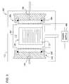
- FIG. 1illustrates one embodiment of a batch processing chamber having an inner chamber 101 (e.g., a quartz chamber), and controlled inject and exhaust.
- the inject assembly 150 and the exhaust assembly 170are temperature controlled to avoid condensation of processing gases.
- FIG. 1is a sectional side view of a batch processing chamber 100 .
- the batch processing chamber 100generally contains an inner chamber 101 defining a process region 117 configured to accommodate a batch of substrates 121 stacked in a substrate boat 120 .
- the substratesare provided in the process region to be processed by various deposition processes, such as an ALD process or a CVD process.
- one or more heater blocksare arranged around the inner chamber 101 and are configured to heat the substrates 121 provided in the process region 117 .
- the inner chamber 101may for example be a quartz chamber.
- An outer chamber 113is generally disposed around the inner chamber 101 .
- One or more thermal insulatorsmay be provided between the outer chamber 113 and any heaters in order to keep the outer chamber cool.
- FIG. 2shows one or more heater blocks 211 , which are arranged around the inner chamber 201 and are configured to heat the substrates provided in the process region.
- An outer chamber 213is generally disposed around the inner chamber 201 .
- the inner chamber 201may, for example, be a quartz chamber.
- thermal insulators 212are be provided between the outer chamber 213 and any heaters in order to keep the outer chamber cool.
- FIG. 1shows the inner chamber 101 , e.g., a quartz chamber, generally containing a chamber body having an opening on the bottom, an injector pocket formed on one side of the chamber body, an exhaust pocket formed on the chamber body on an opposite side of the injector pocket.
- the inner chamber 101has a cylindrical shape similar to that of the substrate boat 120 . Thereby, the process region 117 may be kept small. A reduced process region reduces the amount of processing gas per batch and shortens residence time during batch processing.
- the exhaust pocket 103 and the injector pocket 104may be welded in place with slots milled on the chamber body of inner chamber 101 .
- the injector pocket and the exhaust pocketare flattened quartz tubing with one end welded on the chamber body and one end open.
- the injector pocket 104 and the exhaust pocket 103are configured to house injector assembly 150 and exhaust assembly 170 .
- injector assembly 150 and exhaust assembly 170may typically be temperature controlled.
- a support plate for supporting the inner (quartz) chamberis further connected to a load lock positioned below the bottom opening of inner chamber 101 .
- the substrate boat 120may be loaded and unloaded through the load lock.
- the substrate boat 120may be vertically translated between the process region 117 and the load lock via the opening at the bottom of the inner chamber.
- substrate boatsthat may be used in batch processing chambers and during processes described herein are further described in U.S. Ser. No. 11/216,969, entitled “Batch Deposition Tool and Compressed Boat,” filed Aug. 31, 2005, which is incorporated herein by reference.
- Examples of methods and apparatuses for loading and unloading substrate boats used in batch processingis further described in U.S. Ser. No. 11/242,301, entitled “Batch Wafer Handling System,” filed Sep. 30, 2005, which is incorporated herein by reference.
- the heater blocksare generally wrapped around an outer periphery of the inner chamber 101 except near the injector pocket 104 and the exhaust pocket 103 . According to another embodiment (not shown) the heater blocks 211 may also be wrapped around the injector pocket 104 and/or the exhaust pocket 103 .
- the substrates 121are heated to an appropriate temperature by the heater blocks through the inner chamber 101 .
- the heatersare controlled to achieve uniform heating of the substrates. In one embodiment, points on the substrates 121 in a batch process attain the same set point temperature plus or minus 1 degree Celsius. Configurations of the batch processing chamber 100 improve temperature uniformity in batch processing. For example, a cylindrical shape of the inner chamber 101 results in edges of the substrates 121 evenly distanced from the inner chamber.
- the heatersmay have multiple controllable zones to adjust variations of temperature between regions.
- the heater blocksmay be made of resistive heaters arranged in multiple vertical zones. In one example, the heater blocks may be ceramic resistive heaters.
- FIG. 1illustrates that the injector pocket 104 may be welded on a side of the chamber body defining an inject volume in communication with the process region 117 .
- the inject volumetypically extends along the entire height of the substrate boat 120 when the substrate boat is in a process position.
- the injector assembly 150 disposed in the injector pocketmay, thus, provide a horizontal flow of processing gases to every substrate 121 .
- a recessis formed to hold walls of the injector pocket 104 .
- the injector assemblyis thermally isolated, e.g., by seal 154 .
- Seal 154which may be an o-ring or other suitable elements, also provide a vacuum seal to control the pressure in the inner chamber 101 .
- Thermal isolation of the injector assemblymay be desired to independently control the temperature of the injector.
- an outer volume between inner chamber 101 and chamber 113may also be evacuated. Keeping the outer volume under a reduced pressure may reduce pressure generated stress on inner chamber 101 .
- Additional vacuum sealssuch as o-rings, may be disposed between appropriate parts of chamber 100 , in order to control the pressure of the process region 117 , the vacuum/pressure stress applied to inner chamber 101 , to control gas flow of inserted processing gases only towards the process region.
- one or more vacuum pumpsmay be directly or via additional exhaust plenums (not shown) connected to the inner chamber in order to control the pressure in the inner chamber 101 .
- the temperature of various components in a batch processing chambermay be independently controllable, especially when a deposition process is to be performed in the batch processing chamber. If the temperature of the injector assembly is too low, the gas injected may condense and remain on the surface of the injector assembly, which can generate particles and affect the chamber process. If the temperature of the injector assembly is high enough to evoke gas phase decomposition and/or surface decomposition which may “clog” paths in the injector assembly.
- An injector assembly of a batch processing chamberis heated to a temperature lower than a decomposition temperature of a gas being injected and higher than a condensation temperature of the gas.
- the temperature of the injector assemblyis generally different than the processing temperature in the process region. In one example, substrates may be heated up to about 600 degrees Celsius, while the temperature of the injector assembly is about 80 degrees Celsius during an atomic layer deposition process. Therefore, the temperature of the injector assembly is controlled independently.
- FIG. 1illustrates that the exhaust pocket 103 may be welded on a side of the chamber body defining an exhaust volume in communication with the process region 117 .
- the exhaust volumetypically covers an entire height of the substrate boat 120 when the substrate boat is in a process position such that the exhaust assembly 150 disposed in the exhaust pocket may provide a horizontal flow of processing gases to every substrate 121 .
- a recessis formed to hold walls of the exhaust pocket 103 .
- the exhaust assemblyis thermally isolated, e.g., by seal 174 .
- Seal 174which may be an o-ring or other suitable elements, also provide a vacuum seal to be able to control the pressure in the inner chamber 101 .
- Thermal isolation of the exhaust assemblymay be desired to independently control the temperature of the exhaust.
- an outer volume between inner chamber 101 and chamber 113may also be evacuated. Keeping the outer volume vacuumed can reduce pressure generated stress on the inner chamber 101 .
- Additional vacuum sealssuch as o-rings, may be disposed between appropriate parts of chamber 100 , in order to control the pressure of the process region 117 , the vacuum/pressure stress applied to inner chamber 101 , to control gas flow of inserted processing gases only towards the process region.
- one or more vacuum pumpsmay be directly or via additional exhaust plenums (not shown) connected to the inner chamber in order to control the pressure in the inner chamber 101 .
- Temperature of various components in a batch processing chambermay be controlled independently, especially when a deposition process is to be performed in the batch processing chamber.
- FIG. 1illustrates that additionally a gas source 159 is provided.
- the gas source 159provides processing gas, like precursor gases or deposition gases, treatment gases, carrier gases, and purge gases via valve 158 and via inlet channel 156 into the vertical channel 155 of the injector assembly.
- the vertical channel 155may also be denoted as plenum 155 or cavity 155 .
- the processing gasenters the process region 117 through openings 153 of the injector assembly.
- the plate and openingsform a faceplate 152 to have a uniform distribution of the gas over the substrates 121 in the substrate boat 120 .
- carrier gases and purge gaseswhich may be used as a processing gas, include N 2 , H 2 , Ar, He, combinations thereof, and the like.
- pretreatment steps H 2 , NH 3 , B 2 H 6 , Si 2 H 4 , SiH 6 , H 2 O, HF, HCl, O 2 , O 3 , H 2 O 2 or other known gasesmay be used as a processing gas.
- deposition gases or precursor gasesmay contain a hafnium precursor, a silicon precursor or a combination thereof.
- hafnium precursorsinclude hafnium compounds containing ligands such as halides, alkylaminos, cyclopentadienyls, alkyls, alkoxides, derivatives thereof or combinations thereof.
- Hafnium precursors useful for depositing hafnium-containing materialsinclude HfCl 4 , (Et 2 N) 4 Hf, (Me 2 N) 4 Hf, (MeEtN) 4 Hf, ( t BuC 5 H 4 ) 2 HfCl 2 , (C 5 H 5 ) 2 HfCl 2 , (EtC 5 H 4 ) 2 HfCl 2 , (Me 5 C 5 ) 2 HfCl 2 , (Me 5 C 5 )HfCl 3 , ( i PrC 5 H 4 ) 2 HfCl 2 , ( i PrC 5 H 4 )HfCl 3 , ( t BuC 5 H 4 ) 2 HfMe 2 , (aca
- Alternative metal precursors used during vapor deposition processes described hereininclude ZrCl 4 , Cp 2 Zr, (Me 2 N) 4 Zr, (Et 2 N) 4 Zr, TaF 5 , TaCl 5 , ( t BuO) 5 Ta, (Me 2 N) 5 Ta, (Et 2 N) 5 Ta, (Me 2 N) 3 Ta(N t Bu), (Et 2 N) 3 Ta(NtBu), TiCl 4 , TiI 4 , ( i PrO) 4 Ti, (Me 2 N) 4 Ti, (Et 2 N) 4 Ti, AlCl 3 , Me 3 Al, Me 2 AlH, (AMD) 3 La, ((Me 3 Si)( t Bu)N) 3 La, ((Me 3 Si) 2 N) 3 La, ( t BU 2 N) 3 La, ( i Pr 2 N) 3 La, derivatives thereof or combinations thereof.
- FIG. 1shows only one gas source
- a person skilled in the artwill appreciate that a plurality of gas sources, for example, one gas source for a first precursor, one gas source for a second precursor, and one gas source for a carrier and purge gas, may be coupled to the batch processing chamber 100 .
- a gas flow from the different gasesmay be switched on or off according to the desired needs for a process.
- 3- or 4-way valvesmay be used to provide the different gases to the inlet channel 156 .
- two, three, or more inlet channels 156may milled horizontally across the inject assembly 150 and several vertical channels 155 may be provided to insert different processing gases in the process region.
- inject assembly 250has more than one inlet channel, e.g., three inlet channels 256 , as illustrated in FIG. 2 .
- each of the three inlet channels 256is configured to supply the process region 117 with a processing gas independently from each other.
- Each inlet channel 256is connected to a vertical channel 255 .
- the vertical channels 255may also be denoted as cavities 255 or plenums 255 .
- the vertical channels 255are further connected to a plurality of evenly distributed horizontal holes 253 and form a vertical faceplate on the center portion of the inject assembly 250 .
- an exhaust pocket 103is provided in chamber 101 .
- Exhaust pocketreceives exhaust assembly 170 .
- An exhaust port 176is formed horizontally across the exhaust assembly 170 near a center portion.
- the exhaust port 176opens to a vertical compartment 175 formed in the center portion.
- the vertical compartment 175is further connected to a plurality of horizontal slots 173 which are open to the process region 117 .
- processing gasesfirst flow from the process region 117 to the vertical compartment 175 through the plurality of horizontal slots 173 .
- the processing gasesthen flows into an exhaust system via the exhaust port 176 .
- the horizontal slots 173may vary in size depending on the distance between a specific horizontal slot 173 and the exhaust port 176 to provide an even draw across the substrate boat 120 from top to bottom.
- Processing gasessuch as precursor gases, deposition gases, treatment gases, purge or carrier gases, as described in more detail above, are delivered to and from process region 117 by injector assembly and exhaust assembly.
- a uniform gas flow across each substrate 121 as well as a uniform gas flow across all substrates vertically aligned in the substrate boat 120is desired.
- non-uniformitymight be caused by irregularities in the gas flow at the wafer edges.
- These irregularitiesmay be prevented by providing a diffuser 160 between the injector and the substrate boat.
- the diffuser 160may prevent the gas flow from direct impact on the edge of the substrate.
- Diffuser 160may have a V-shaped form and may direct gas from the inlet tangentially along the substrates.
- the diffusermay be provided in various shapes and positions. Generally, the diffuser may be provided between the faceplate of the injector assembly and the substrate boat. Thereby, the diffuser may be integrated in the substrate assembly and/or may be positioned in the injector pocket of the inner chamber 101 .
- Various embodiments of diffusers which may be used in chambers and methods of the applicationare described in more detail in U.S. patent application, entitled: “Batch Processing Chamber with Diffuser Plate and Injector Assembly”, filed on an even dated herewith (U.S. patent application Ser. No. 11/381,966), which is incorporated herein by reference.
- the gas flow with improved uniformitycarries ionized species of the processing gases, like precursor gases or carrier or purge gases.
- the uniformity of the gas flowalso improves the uniformity of the ionized species, which are used to provide plasma assisted, UV assisted, or ion assisted processes.
- the process assistance by plasma, UV, ion generationcan be characterized as exciting the introduced gas or by ionizing the introduced gases.
- the components providing the processing gas flow to the process region 117are configured to form a uniformly deposited material across each substrate and across the substrates in the substrate boat.
- Plasma assisted batch processinghas previously been conducted with a remote plasma source.
- a remote plasmais generated at larger distances with regard the process region.
- the number of excited species within the plasmahas already considerably decreased as the plasma enters the process region.
- a remote plasma sourceresults in a relaxation of the plasma before the plasma enters the process region.
- the inventiongenerally provides an apparatus and a method for processing semiconductor substrates in a batch tool, in which, e.g., the plasma for plasma assisted processing of substrates is provided in the process region or close or adjacent to the process region. Close or adjacent to the process region is to be understood as having the plasma generation directly neighboring the process region, or at least within the inner chamber, the injector pocket, or the injector assembly.
- An embodiment illustrated in FIG. 1includes a power source 180 to generate a plasma, which is connected to the diffuser 160 and the faceplate 152 of the injector assembly 150 .
- a plasmais generated between the diffuser 160 and the faceplate 152 of the injector assembly 150 .
- the injector faceis used as an anode and the diffuser is used as a cathode to generate a plasma therebetween.
- the power applied to generate the plasmacan be adapted to the desired application and may depend on the energy necessary to ionize particular species in the processing gas flowing into the process region. As a result, the plasma power may vary depending on the process step presently conducted.
- a different powermaybe applied during a gas flow of a first precursor, during purging or pumping to remove the first precursor, during gas flow of a second precursor and during purging or pumping to remove the second precursor.
- some of the process stepsmay be conducted at similar plasma power or without plasma assistance.
- the purge stepsmay be conducted with the same power or without power, whereas for the times when precursors are provided to the process region, plasma power adapted for the first and second precursor, respectively, is applied.
- barrier seal 154is disposed between the inject pocket 104 and the inject assembly 150
- barrier seal 174is disposed between the exhaust pocket 103 and the exhaust assembly 170 .
- processing chemicalsare prevented from entering any undesirable areas in the batch processing chamber.
- a vacuum seal for the quartz chambermay be provided by seals 154 , 174 .
- the sealswhich may be provided in the form of O-rings or the like, can electrically insulate different components within the chamber from each other. This is of increasing relevance as the power provided by power supply 180 increases. Higher voltages applied to electrodes, e.g., the injector assembly, may require improved electrical insulation of the injector assembly.
- the plasmamay be confined between the face of the injector assembly 150 and the diffuser 160 . Thereby, direct exposure of the substrate to a plasma may be avoided. This might be desirable to prevent plasma damage to the surfaces of the substrates. Accordingly, the diffuser shields the substrates from the plasma.
- a plasmais generated in the horizontal direction.
- the plasmaextends along the vertical direction of the diffuser 160 and the injector assembly 150 .
- the horizontal plasmaextends along the vertical direction of the process region 117 .
- the substrates 121 in the substrate boat 120are exposed to the plasma along the entire stack of substrates.
- the previously described uniform gas flowprovides a uniform distribution of ionized species of the plasma across the wafers.
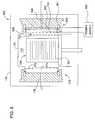
- FIG. 2illustrates a further embodiment of a batch processing chamber having an inner chamber 201 , and controlled inject and exhaust.
- the injector assembly 250 and the exhaust assembly 270are temperature controlled to avoid condensation of processing gases.
- FIG. 2is a sectional top view of a batch processing chamber 200 .
- the batch processing chamber 200generally contains an inner chamber 201 defining a process region 217 configured to accommodate a batch of substrates stacked in a substrate boat 220 .
- the substratesare provided in the process region to be processed by various deposition processes, such as an ALD process or a CVD process.
- one or more heater blocks 211which are arranged around the inner chamber 201 and are configured to heat the substrates provided in the process region.
- An outer chamber 213is generally disposed around the inner chamber 201 .
- thermal insulators 212are provided between the outer chamber 213 and any heaters in order to keep the outer chamber cool.
- the inner chamber 201e.g., a quartz chamber, generally comprises a chamber body having an opening on the bottom, an injector pocket formed on one side of the chamber body, an exhaust pocket formed on the chamber body on an opposite side of the injector pocket.
- the inner chamber 201has a cylindrical shape similar to that of the substrate boat 220 . Thereby, the process region 117 is kept relatively small. A reduced process region reduces the amount of processing gas per batch and shortens residence time during batch processing.
- the exhaust pocket 203 and the injector pocket 204may be welded in place with slots milled on the chamber body.
- the exhaust pocketmay be provided in the form of vertically aligned tubes connecting the processing region with the vertical compartment 275 .
- the injector pocket 204 and the exhaust pocket 203are flattened quartz tubing with one end welded on the chamber body and one end open.
- the injector pocket 204 and the exhaust pocket 203are configured to house injector assembly 250 and exhaust assembly 270 . Injector assembly 250 and exhaust assembly 270 are typically temperature controlled.
- An embodiment illustrated in FIG. 2includes a power source 280 to generate a plasma, which is connected to the diffuser 260 and the faceplate 252 of the injector assembly 250 .
- a plasmais generated between diffuser 260 and the face of the injector assembly.
- the injector faceis used as an anode and the diffuser is used as a cathode to generate a plasma therebetween.
- the power applied to generate the plasmacan be adapted to the desired application and may depend on the energy necessary to ionize particular species in the processing gas flowing into the process region. As a result, the plasma power may vary depending on the process step presently conducted. For example, for a plasma assisted ALD process, a different power maybe applied during a gas flow of a first precursor, during purging or pumping to remove the first precursor, during gas flow of a second precursor and during purging or pumping to remove the second precursor.
- some of the process stepsmay be conducted at similar plasma power or without plasma assistance.
- the purge stepsmay be conducted with the same power or without power, whereas plasma power adapted for the first and second precursor, respectively, is applied during the injection of the respective precursor gases.
- the plasmamay be confined between the face of the injector assembly 250 and the diffuser 260 .
- the diffusershields the substrates from the plasma.
- a plasma in horizontal directionis generated.
- the plasmaextends along the vertical direction of the diffuser and the injector assembly.
- the horizontal plasmaextends along the vertical direction of the process region 217 .
- the substrates in the substrate boat 220are exposed to the plasma along the entire stack of substrates.
- the previously described uniform gas flowprovides a uniform distribution of ionized species of the plasma across the wafers.
- the batch processing chamber 200includes an outer chamber 213 , heater blocks 211 separated from the outer chamber by thermals insulators 212 .
- An inner chamber 201 including injector pocket 204 and exhaust pocket 203 or exhaust tubessurrounds substrate boat 220 located in the process region.
- the injector assembly 250has three inlet channels 256 . Processing gas can be provided through the channels to vertical channels 255 and enters the processing location through openings 253 in the face of injector assembly 250 .
- the exhaust assembly 270includes exhaust port 176 , vertical compartment 275 and horizontal slots 273 .
- a v-shaped diffuser 260is shown.
- a power sourceis coupled via the injector assembly to the injector face and the diffuser to generate a plasma between the injector face and the diffuser.
- FIG. 2further illustrates a conductive mesh 261 that further confines the plasma in the gap between the diffuser and the injector face.
- the diffusermay additionally be made permeable to confine the plasma and to improve protection of the substrates from energetic particles.
- a permeable diffusermay improve the uniformity of the gas flow across the wafer.
- the diffusermay be provided in the form of a mesh.
- mesh 261 and a permeable mesh diffuser 260may be provided as one unit to provide a cathode and to confine the plasma between this cathode and the face of the injector assembly acting as the anode.
- the conductive and permeable mesh, the diffuser and the face of the injector assemblyextend along the direction in which the substrates are stacked over each other in the substrate boat. In the embodiments shown herein, this direction is the vertical direction.
- the substratesare vertically stacked.
- FIG. 3illustrates another embodiment of a batch processing chamber 300 wherein plasma assisted ALD processes, plasma assisted CVD processes or other plasma assisted processes may be conducted.
- FIG. 3elements that are the same in the embodiment of FIG. 1 are denoted with the same reference numbers. Alternatively, these elements may be the same as in the embodiment shown in FIG. 2 . A repetition of the description of these elements and the related purposes or usage is omitted for simplicity.
- a power supply 380is connected to the injector assembly 350 and the exhaust assembly 370 in order to generate a plasma between the face of the injector and the opposing port of the exhaust.
- the plasmais generated horizontally, that is parallel to the surfaces of the substrates.
- the plasmaextends along the process region 117 of the inner chamber 101 .
- the exhaust portmay be used as the cathode and the face of the injector assembly may be used as the anode.
- the voltage provided by the power supply between the cathode and the anodehas to be increased in order to provide the same electrical field acting on the species of the processing gas.
- the charged componentsmay need further electrical isolation from surrounding components. In FIG. 3 , this is indicated by an increased gap between the injector assembly 350 and the injector pocket of the inner chamber 101 . Further, the gap of the exhaust assembly 370 is increased.
- Seals 354 and 374are also increased in size to indicate the further electrical insulation. Even though, in the case of a quartz chamber, an insulation of the face of the injector assembly and the port of the exhaust assembly may partly be provided by the non-conductive inner chamber, potentials sufficiently high to create a plasma across the process region may need additional insulation of components in the batch processing chamber 300 .
- FIG. 4A further embodiment of a batch processing chamber 400 providing the option of conducting plasma assisted processes is shown in FIG. 4 .
- elements that are the same in the embodiments of FIG. 1 or other previous embodimentsare denoted with the same reference numbers. Alternatively, these elements may be the same as in the embodiment shown in FIG. 2 . A repetition of the description of these elements and the related purposes or usage is omitted for simplicity.
- an electrode 470is positioned in the inner chamber 101 .
- the electrode 470 or the electrodes 470may be provided in the form of a rod disposed within the chamber cavity adjacent to the exhaust assembly.
- Power supply 480is connected to electrodes 470 and to the injector assembly 350 .
- the faceplate of the injector assemblyacts as an electrode.
- a plasmais generated horizontally, parallel to the substrate surfaces of the substrates in the substrate boat. The generated plasma extends across the process region and is exposed to the substrates.
- FIG. 4shows three rods 470 as electrodes for plasma generation.
- one or two vertical rodsmay also be used as electrodes.
- 4 or more rodsmay be used as electrodes.
- the number and the arrangement of electrodesshould be adapted to provide a uniform plasma across the substrates and to not disturb the uniformity of the gas flow of the processing gases.
- the rodsmay also be positioned between the face of the injector assembly and the substrate boat.
- a plasma generation comparable to FIG. 1may occur.
- the plasmais generated adjacent the substrate boat within inner chamber 101 , e.g., a quartz chamber.
- the plasmais generated horizontally between the vertically extending face of the injector assembly and the vertically extending set of rods.
- electrodesmay also be disposed at other locations in the inner chamber 101 .
- FIGS. 5 and 6illustrate further embodiments. Elements that are the same in the embodiments of FIG. 1 or other previous embodiments are denoted with the same reference numbers. Alternatively, these elements may be the same as in the embodiment shown in FIG. 2 . A repetition of the description of these elements and the related purposes or usage is omitted for simplicity.
- the plasmamay be generated in the injector assembly.
- the plasmamay be generated in the vertical channel inside the injector assembly.
- the vertical channelmay be denoted as plenum or cavity.
- FIG. 5shows a batch processing chamber.
- the injector assembly 550includes vertical rods 553 insulated from each other by insulator parts 559 .
- the injector 550may be formed of an insulating material.
- a plasma power source 580is connected to the top rod 553 and the bottom rod 553 .
- the top rodmay be the cathode and the bottom rod may be the cathode, whereas to another embodiment the top rod may be the cathode whereas the bottom rod is the anode.
- the rodsform electrodes for generation of a plasma.
- the generated plasmais confined in the vertically extending channels 555 .
- the plasmais generated vertically and the excited species of the processing gas enter the process region horizontally through the openings in the faceplate of the injector assembly.
- the faceplate of the injectormay be made of a conductive material to improve confinement of the plasma within the vertical channel.
- the embodiments described with respect to FIG. 5may optionally include a diffuser 160 as shown in FIG. 5 and described in more detail with respect to FIGS. 1 and 2 .
- the embodiment shown in FIG. 6also includes plasma generating elements that provide a plasma in the vertical channel of the injector assembly 650 .
- the plasmais generated between the walls of the vertical channel.
- One wallis the faceplate 152 including the openings 153 .
- the other wallis electrode 652 is provided in the body 651 of injector assembly 650 . Electrode 652 forms the wall of the vertical channel opposing the faceplate 152 .
- the two electrodes connected to the power supply 680are separated by insulator element 659 .
- the body 651 of the injector assemblymay form one of the electrodes to generate the plasma.
- the injectoris formed of a conductive material and no separate electrode 652 may be required.
- the faceplate forming the opposing electrodewould also be connected to the body 651 by insulating elements 659 .
- the embodiments described with respect to FIG. 6may optionally include a diffuser 160 as shown in FIG. 5 and described in more detail with respect to FIGS. 1 and 2 .
- Embodiments described herein with respect to FIGS. 1 to 6illustrate batch processing chambers which may be used during plasma assisted processes, e.g., ALD or CVD processes.
- the plasma assistanceprovides ionized species of the processing gases within the chamber and in or in the vicinity of the process region.
- the presence of the plasma in the process region or in the vicinity of the process regionreduces relaxation of the excited states. Since the plasma assistance provides ionized species of the processing gases to the substrate surfaces, a plasma assisted process can be considered one form of process based on excited species of the processing gases.
- the processesare assisted by UV radiation.
- the UV lightmay be used to excite and/or ionize species of the processing gases or, e.g., to maintain the O 3 concentration at a desired level.
- UV assistance during batch processingmay also be considered one form of process that is assisted by excited species.
- species of the processing gasesare excited above ground state.
- the excitationdepends on the wavelength of the UV light.
- the wavelengthmay be in the range of 126 nm to 400 nm.
- the excited speciesassist ALD or CVD processes by initiating or enhancing surface reactions of the precursors or reactance.
- the enhancementmay result in reduction of exposure time and, thus, increase throughput. Additionally, film quality may improve because of more complete reactions of the precursors.
- the relaxation time of the excited speciesmay be in a range that by the time the processing gas reaches the process region a remotely excited processing gas has relaxed.
- the O 3 concentrationmight decrease by the time it reaches the process region of the deposition chamber if excited at a remote location.
- the O 3 concentrationmay be maintained higher by activating O 3 inside the chamber.
- FIG. 7An embodiment of a batch processing chamber 700 with UV assistance is shown in FIG. 7 .
- elements that are the same in the embodiments of FIG. 1 or other previous embodimentsare denoted with the same reference numbers. Alternatively, these elements may be the same as in the embodiment shown in FIG. 2 . A repetition of the description of these elements and the related purposes or usage is omitted for simplicity.
- FIG. 7illustrates an embodiment for irradiating UV light vertically inside the vertical channel 755 of the injector assembly 750 .
- a UV source 790is provided at the upper end of the vertical channel 755 and a UV source is provided at the lower end of the vertical channel.
- Each sourceincludes a lamp 792 and a window 793 facing the vertical channel.
- the window materialcan be chosen depending from the UV wavelength. For example a quartz window may be used for wavelength up to about 180 nm to 220 nm. Sapphire., magnesium fluoride or calcium fluoride windows may be used as window 793 in the event of shorter wavelengths.
- the UV lightextends vertically along the vertical channel 755 and excites species of the processing gases in the injector assembly before entering the process region.
- UV lampslike deuterium lamps or arc lamps filled with Hg or Xe, may be used.
- the species of the processing gas excited in the vertical channelare provided uniformly with the uniform gas flow generated by the injector assembly, the exhaust assembly and optionally be the diffuser, the gas flow being described in more detail with respect to FIG. 1 .
- FIG. 8shows another embodiment of batch processing chamber 800 with an injector assembly 850 .
- the embodimentmay be used for UV assisted processes.
- elements that are the same in the embodiments of FIG. 1 or other previous embodimentsare denoted with the same reference numbers. Alternatively, these elements may be the same as in the embodiment shown in FIG. 2 . A repetition of the description of these elements and the related purposes or usage is omitted for simplicity.
- FIG. 8illustrates that the injector assembly shines UV light through openings 153 of the faceplate horizontally and parallel to substrate surfaces of substrates stacked in a substrate boat.
- the UV lightis generated in the vertical channel 855 by striking a glow discharge with a noble gas in vertical channel 855 .
- the injector face 852 of the faceplateis configured as an anode.
- the body 851 of the injectoris electrically insulated by insulators 859 from the anode.
- the vertical channel 855functions as a hollow cathode.
- the injector assemblymay have a plurality of vertical channels.
- a single one of the vertical channels or a plurality of vertical channelsmay be used as a hollow cathode to provide UV light inside the chamber.
- tips 854can be mounted in the injector. Thereby, the electrical field strength near the tips is increased and the glow discharge can be ignited with smaller voltages applied. According to another embodiment (not shown) the tips 854 may be omitted if sufficient power is provided by power source 880 to strike the glow discharge in the vertical channel.
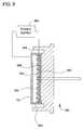
- FIG. 9shows another embodiment of an injector assembly.
- a separate conductive element 950is provided at the rear end of the vertical channel as the cathode.
- the cathode 950is provided with a plurality of small cavities. These cavities are in the form of cylinders with a small diameter in the range of 1 mm to 12 mm, are provided as an array of additional hollow cathodes.
- the hollow cathode effectproviding the UV light with a wavelength corresponding to the gas in the vertical channel and/or the cathode material can be multiplied.
- the photon density in the vertical channel and in the process region wherein the substrates are processedcan be increased. Alignment between hollow cathodes and the faceplate holes ensures that transmission into the process region is optimized.
- Tips 954may be provided in the hollow cathodes. The tips may be used to increase the electrical field strength due to the small curvature of the tip and improve striking of a glow discharged at lower voltage levels.
- a glow dischargemay also be generated between the diffuser and the face of the injector, that is one side of the faceplate.
- the diffuseris provided as the anode and the face of the injector is the cathode.
- differential pumpingmay be used (not shown).
- the process pressure at the substratesmay be lower than the pressure required by the glow discharge used for UV production.
- gas used for glow dischargemay be diverted from the process chamber.
- an UV transparent membranemay be fastened to the reactor side of the injector faceplate (not shown.)
- the process pressure at the substratesmay be higher than the pressure required by the glow discharge used for UV production.
- gas from the processis isolated from the gas used for glow discharge by a barrier. Since the barrier is UV transparent, UV is transmitted to the substrates. The barrier is thin to optimize UV transmission, but thick enough to support a process pressure of up to about 10 Torr.
- the wavelength of the UV raditionmay be selected based on the gases used in the hollow cathode.
- Typical noble gases and their irradiated photon energy based on recombination of the excited statesare He (for example, 21.22 eV, 40.82 eV, 40.38 eV), Ne (for example, 16.85 eV, 16.67 eV, 26.9 eV) or Ar (for example, 11.83 eV, 11.63 eV, 13.48 eV, 13.30 eV).
- Hefor example, 21.22 eV, 40.82 eV, 40.38 eV
- Nefor example, 16.85 eV, 16.67 eV, 26.9 eV
- Arfor example, 11.83 eV, 11.63 eV, 13.48 eV, 13.30 eV.
- Broad spectrum UV from deuterium lamps, or other UV sources (for example a mercury lamp), as well as softer UV radiationis also applicable.
- a susceptor for carrying the substrates formed of silicon carbide (SiC)may be adapted to reflect the UV light.
- the susceptor profile and the roughnessmay be adapted to reflectively focus the UV light on the substrate surfaces.
- the cylindrical geometry of the inner chamber 101favors glancing angles for which UV reflectivity is enhanced relative to normal incidence.
- UV assistingmay be provided during any process step having appropriate conditions for the glow discharge.
- conditions in the plenum of the injector and the processing regionmay vary if a gas diversion, a barrier or other measures are provided.
- conditions appropriate for glow dischargemay be provided in the parts of the chamber.
- Appropriate process conditionsmay include the injection of a gas desired for the glow discharge.
- a gas desired for the glow dischargeFor 11.63 eV and 11.83 eV photons from Ar, an optimal pressure of the glow discharge is 0.45 Torr, and the reflectivity for SiC is 0.4 at normal incidence and at ⁇ /4 incidence.
- UV assistancemay be required for one or all precursor exposures where the photon energy may be required to start the reaction between precursor molecule and surface binding site. UV assistance may be required during the cycle-purging steps at the end of an ALD cycle to complete the surface reaction such that incorporation of reaction byproducts is minimized.
- UV assisted processescan be provided with a vertically extending anode and a vertically extending hollow cathode, wherein the anode and the cathode is arranged such that the anode is closer to the substrate boat holding the wafer stack.
- a diffuserwould be the cathode and the injector face would be the anode.
- the injector face side of the vertical channel(faceplate side of the vertical channel) would be the cathode and the opposing side of the injector located towards the body of the injector assembly would be the anode.
- the power supplyis connected to the respective components of the previous embodiments with a polarization, such that ions are provided to the processing region.
- ion generating assistance during batch processingmay also be considered one form of process assisted by excited species.
- the diffusermay be modified to provide a hollow cathode effect.
- Ions generated in the glow dischargeare then accelerated towards the process region.
- Ions and neutralsmay pass the cathode through openings provided therein.
- the ions and neutralsenter the process region and can assisted processes by the energy or the momentum of the ions.
- the kinetic energy of the ions and neutralsmay be about 600 eV.
- retarding gridsmay be used to reduce the ion energy.
- a retarding gridmay be provided in form of a mesh with a potential applied thereto. The potential decelerates the ions.
- the decelerated ionsmay pass through openings in the grid.
- a charged grid mounted between the injector and the wafer boatcan, thus, reduce the energy and the momentum to a desired level.
- the electrode formed by the elements of the injector and the exhaustmay be grounded, whereas the other electrode is biased.
- Elements of the injector or exhaust assemblymay be an anode or a cathode for plasma generation, UV generation or ion generation. Generally, it is to be understood that either one of the anode or the cathode may be grounded.
Landscapes
- Chemical & Material Sciences (AREA)
- Engineering & Computer Science (AREA)
- General Chemical & Material Sciences (AREA)
- Chemical Kinetics & Catalysis (AREA)
- Materials Engineering (AREA)
- Mechanical Engineering (AREA)
- Metallurgy (AREA)
- Organic Chemistry (AREA)
- Physics & Mathematics (AREA)
- Plasma & Fusion (AREA)
- Analytical Chemistry (AREA)
- Chemical Vapour Deposition (AREA)
Abstract
Description
- 1. Field of the Invention
- Embodiments of the invention generally relate to an apparatus and a method used during a batch deposition process, and more specifically, embodiments relate to a batch processing chamber and a batch processing method for depositing a material using a processing gas having excited species.
- 2. Description of the Related Art
- A substrate fabrication process is often evaluated by two related and important factors, which are device yield and the cost of ownership (COO). The COO, while affected by a number of factors, is greatly affected by the number of substrates processed per time, i.e., the throughput of the fabrication process, and cost of processing materials. Batch processing has been found to be promising in the attempt to increase throughput. However, providing processing conditions uniformly over an increased number of substrates is a challenging task.
- In addition, plasma assisted ALD or CVD processes, UV assisted (photo-assisted) ALD or CVD processes, and ALD or CVD processes having assistance directly by ions provided to a processing area have been shown to be beneficial to some deposition processes. For example, UV and plasma assisted processes have been demonstrated to provide good film quality for high-k dielectrics which are increasingly needed as device scale approaches sub 65 nm applications. Plasma assisted ALD or CVD have also been demonstrated to reduce thermal budget and process time requirements as compared to similar thermally assisted processes.
- Providing uniform process conditions over an increased number of substrates is even more challenging if additional assisting treatments are added to the processes as described above for plasma assisted ALD or CVD processes, UV assisted (photo-assisted) ALD or CVD processes, and ALD or CVD processes having assistance directly by ions provided to a processing area.
- Plasma assisted ALD processes have used remote plasma generation to attempt exposing substrates to uniform plasma conditions within a batch chamber. The plasma is introduced through a delivery system such as the gas delivery system of the batch tool. However, this process may suffer from the relaxation of the plasma prior to entering the process region.
- Therefore, there is a need for an apparatus and a method for uniformly and effectively depositing materials during ALD or CVD processes in a batch tool with plasma assistance, UV assistance, or ion assistance.
- The invention generally provides a batch processing apparatus in which a plurality of substrates is processed in parallel. The apparatus includes an assembly for exciting species of the one or more processing gases used for processing the substrates by a plasma assistance, a UV assistance and/or an ion assistance. Embodiments of the invention generally provide methods of the assisted processes and apparatuses, in which the assisted processes may be conducted for providing uniformly deposited material.
- According to one embodiment, a batch processing chamber is provided which includes a chamber housing of the batch chamber, a substrate boat for containing a batch of substrates in a process region, and an excitation assembly for exciting species of a processing gas. The excitation assembly is positioned within the chamber housing.
- According to another embodiment, a method for batch processing of substrates is provided which includes processing a batch of substrates vertically stacked in a substrate boat positioned within a chamber, injecting processing gases into a process region within the chamber, and assisting the processing by exciting species of the processing gas within the chamber.
- So that the manner in which the above recited features of the invention can be understood in detail, a more particular description of the invention, briefly summarized above, may be had by reference to embodiments, some of which are illustrated in the appended drawings. It is to be noted, however, that the appended drawings illustrate only typical embodiments of this invention and are therefore not to be considered limiting of its scope, for the invention may admit to other equally effective embodiments.
FIG. 1 illustrates a sectional side view of an exemplary batch processing chamber of the invention including an assembly for exciting species of the processing gases.FIG. 2 illustrates a sectional top view of a further embodiment of a batch processing chamber of the invention including an assembly for exciting species of the processing gases.FIG. 3 illustrates a sectional side view of an embodiment of a batch processing chamber of the invention including an assembly for exciting species of the processing gases within a process region.FIG. 4 illustrates a sectional side view of another embodiment of a batch processing chamber of the invention including an assembly for exciting species of the processing gases within a process region.FIG. 5 illustrates a sectional side view of an exemplary batch processing chamber of the invention including an assembly for exciting species of the processing gases within an injector assembly.FIG. 6 illustrates a sectional side view of another embodiment of an exemplary batch processing chamber of the invention including an assembly for exciting species of the processing gases within an injector assembly.FIG. 7 illustrates a sectional side view of an even further embodiment of an exemplary batch processing chamber of the invention including an assembly for exciting species of the processing gases within an injector assembly.FIG. 8 illustrates a sectional side view of another embodiment of an exemplary batch processing chamber of the invention including an assembly for exciting species of the processing gases within an injector assembly.FIG. 9 illustrates a sectional side view of another embodiment of an injector assembly for a batch processing chamber of the invention including an assembly for exciting species of the processing gases within an injector assembly.- The invention generally provides an apparatus and a method for processing semiconductor substrates in a batch with assemblies for assisting the processes by generated ions. In one embodiment of the invention, a batch processing chamber with an excitation assembly, which is positioned within the batch processing chamber housing, is provided. An example of a batch processing chamber which may be useful for one embodiment described herein is a FLEXSTAR® system, available from Applied Materials, Inc., located in Santa Clara, Calif.
- Generally, excited species of processing gases may be generated to assist the ALD or CVD processes as described herein. These species may be excited by plasma assistance, UV assistance (photo assistance), ion assistance (e.g., ions generated by an ion source), or combinations thereof. The species are excited in or in the vicinity of the process region within the chamber housing to avoid relaxation of the excited states before the ions reach the process region of the batch processing chamber.
- A “substrate” as referred to herein, includes, but is not limited to, semiconductor wafers, semiconductor workpieces, and other workpieces such as optical planks, memory disks and the like. Embodiments of the invention may be applied to any generally flat workpiece on which material is deposited by the methods described herein.
- “Vertical direction” and “horizontal direction” are to be understood as indicating relative directions. Thus, the horizontal direction is to be understood as substantially perpendicular to the vertical direction and vice versa. Nevertheless, it is within the scope of the invention that the described embodiments and aspects may be rotated in its entirety such that the dimension referred to as the vertical direction is oriented horizontally and, at the same time, the dimension referred to as the horizontal direction is oriented vertically.
- A batch processing chamber for ALD or CVD processing useful for embodiments described herein is described in commonly assigned U.S. Ser. No. 11/249,555, entitled “Reaction Chamber with Opposing Pockets for Gas Injection and Exhaust,” filed Oct. 13, 2005, which is incorporated herein by reference for providing further description of a chamber, a heating system, a gas delivery system, and an exhaust system.
FIG. 1 illustrates one embodiment of a batch processing chamber having an inner chamber101 (e.g., a quartz chamber), and controlled inject and exhaust. Typically, theinject assembly 150 and theexhaust assembly 170 are temperature controlled to avoid condensation of processing gases.FIG. 1 is a sectional side view of abatch processing chamber 100. Thebatch processing chamber 100 generally contains aninner chamber 101 defining aprocess region 117 configured to accommodate a batch ofsubstrates 121 stacked in asubstrate boat 120. The substrates are provided in the process region to be processed by various deposition processes, such as an ALD process or a CVD process. Generally, one or more heater blocks (not shown) are arranged around theinner chamber 101 and are configured to heat thesubstrates 121 provided in theprocess region 117. In one embodiment, theinner chamber 101 may for example be a quartz chamber. Anouter chamber 113 is generally disposed around theinner chamber 101. One or more thermal insulators (not shown) may be provided between theouter chamber 113 and any heaters in order to keep the outer chamber cool.- An example of the heater blocks and the thermal insulators, which may be used in the embodiment shown in
FIG. 1 , is shown in the embodiment ofFIG. 2 .FIG. 2 , shows one ormore heater blocks 211, which are arranged around the inner chamber201 and are configured to heat the substrates provided in the process region. Anouter chamber 213 is generally disposed around the inner chamber201. In one embodiment, the inner chamber201 may, for example, be a quartz chamber. InFIG. 2 ,thermal insulators 212 are be provided between theouter chamber 213 and any heaters in order to keep the outer chamber cool. FIG. 1 shows theinner chamber 101, e.g., a quartz chamber, generally containing a chamber body having an opening on the bottom, an injector pocket formed on one side of the chamber body, an exhaust pocket formed on the chamber body on an opposite side of the injector pocket. Theinner chamber 101 has a cylindrical shape similar to that of thesubstrate boat 120. Thereby, theprocess region 117 may be kept small. A reduced process region reduces the amount of processing gas per batch and shortens residence time during batch processing.- In one embodiment, the
exhaust pocket 103 and theinjector pocket 104 may be welded in place with slots milled on the chamber body ofinner chamber 101. According to one embodiment, the injector pocket and the exhaust pocket are flattened quartz tubing with one end welded on the chamber body and one end open. Theinjector pocket 104 and theexhaust pocket 103 are configured to houseinjector assembly 150 andexhaust assembly 170. As described in more detail in U.S. Ser. No. 11/249,555, entitled “Reaction Chamber with Opposing Pockets for Gas Injection and Exhaust,” filed Oct. 13, 2005, incorporated by reference above,injector assembly 150 andexhaust assembly 170 may typically be temperature controlled. Further, a support plate for supporting the inner (quartz) chamber is further connected to a load lock positioned below the bottom opening ofinner chamber 101. Thesubstrate boat 120 may be loaded and unloaded through the load lock. Thesubstrate boat 120 may be vertically translated between theprocess region 117 and the load lock via the opening at the bottom of the inner chamber. - Examples of substrate boats that may be used in batch processing chambers and during processes described herein are further described in U.S. Ser. No. 11/216,969, entitled “Batch Deposition Tool and Compressed Boat,” filed Aug. 31, 2005, which is incorporated herein by reference. Examples of methods and apparatuses for loading and unloading substrate boats used in batch processing is further described in U.S. Ser. No. 11/242,301, entitled “Batch Wafer Handling System,” filed Sep. 30, 2005, which is incorporated herein by reference.
- The heater blocks are generally wrapped around an outer periphery of the
inner chamber 101 except near theinjector pocket 104 and theexhaust pocket 103. According to another embodiment (not shown) the heater blocks211 may also be wrapped around theinjector pocket 104 and/or theexhaust pocket 103. Thesubstrates 121 are heated to an appropriate temperature by the heater blocks through theinner chamber 101. The heaters are controlled to achieve uniform heating of the substrates. In one embodiment, points on thesubstrates 121 in a batch process attain the same set point temperature plus or minus 1 degree Celsius. Configurations of thebatch processing chamber 100 improve temperature uniformity in batch processing. For example, a cylindrical shape of theinner chamber 101 results in edges of thesubstrates 121 evenly distanced from the inner chamber. Also, the heaters may have multiple controllable zones to adjust variations of temperature between regions. The heater blocks may be made of resistive heaters arranged in multiple vertical zones. In one example, the heater blocks may be ceramic resistive heaters. FIG. 1 illustrates that theinjector pocket 104 may be welded on a side of the chamber body defining an inject volume in communication with theprocess region 117. The inject volume typically extends along the entire height of thesubstrate boat 120 when the substrate boat is in a process position. Theinjector assembly 150 disposed in the injector pocket may, thus, provide a horizontal flow of processing gases to everysubstrate 121.- A recess is formed to hold walls of the
injector pocket 104. The injector assembly is thermally isolated, e.g., byseal 154.Seal 154, which may be an o-ring or other suitable elements, also provide a vacuum seal to control the pressure in theinner chamber 101. Thermal isolation of the injector assembly may be desired to independently control the temperature of the injector. - Since the
process region 117 and the injector volume are usually kept in a vacuum state during process, an outer volume betweeninner chamber 101 andchamber 113 may also be evacuated. Keeping the outer volume under a reduced pressure may reduce pressure generated stress oninner chamber 101. Additional vacuum seals, such as o-rings, may be disposed between appropriate parts ofchamber 100, in order to control the pressure of theprocess region 117, the vacuum/pressure stress applied toinner chamber 101, to control gas flow of inserted processing gases only towards the process region. Further, one or more vacuum pumps may be directly or via additional exhaust plenums (not shown) connected to the inner chamber in order to control the pressure in theinner chamber 101. - The temperature of various components in a batch processing chamber may be independently controllable, especially when a deposition process is to be performed in the batch processing chamber. If the temperature of the injector assembly is too low, the gas injected may condense and remain on the surface of the injector assembly, which can generate particles and affect the chamber process. If the temperature of the injector assembly is high enough to evoke gas phase decomposition and/or surface decomposition which may “clog” paths in the injector assembly. An injector assembly of a batch processing chamber is heated to a temperature lower than a decomposition temperature of a gas being injected and higher than a condensation temperature of the gas. The temperature of the injector assembly is generally different than the processing temperature in the process region. In one example, substrates may be heated up to about 600 degrees Celsius, while the temperature of the injector assembly is about 80 degrees Celsius during an atomic layer deposition process. Therefore, the temperature of the injector assembly is controlled independently.
FIG. 1 illustrates that theexhaust pocket 103 may be welded on a side of the chamber body defining an exhaust volume in communication with theprocess region 117. The exhaust volume typically covers an entire height of thesubstrate boat 120 when the substrate boat is in a process position such that theexhaust assembly 150 disposed in the exhaust pocket may provide a horizontal flow of processing gases to everysubstrate 121.- A recess is formed to hold walls of the
exhaust pocket 103. The exhaust assembly is thermally isolated, e.g., byseal 174.Seal 174, which may be an o-ring or other suitable elements, also provide a vacuum seal to be able to control the pressure in theinner chamber 101. Thermal isolation of the exhaust assembly may be desired to independently control the temperature of the exhaust. - Since the
process region 117 and the exhaust volume are usually kept in a vacuum state during process, an outer volume betweeninner chamber 101 andchamber 113 may also be evacuated. Keeping the outer volume vacuumed can reduce pressure generated stress on theinner chamber 101. Additional vacuum seals, such as o-rings, may be disposed between appropriate parts ofchamber 100, in order to control the pressure of theprocess region 117, the vacuum/pressure stress applied toinner chamber 101, to control gas flow of inserted processing gases only towards the process region. Further, one or more vacuum pumps may be directly or via additional exhaust plenums (not shown) connected to the inner chamber in order to control the pressure in theinner chamber 101. - Temperature of various components in a batch processing chamber may be controlled independently, especially when a deposition process is to be performed in the batch processing chamber. On the one hand, it is desirable to keep the temperature in the exhaust assembly lower than the temperature in the processing chamber such that the deposition reactions do not occur in the exhaust assembly. On the other hand, it is desirable to heat an exhaust assembly such that processing gases passing the exhaust assembly do not condense and remain on the surface causing particle contamination. If deposition of reaction byproducts on the exhaust assembly does occur, then elevated temperatures on the exhaust assembly may ensure that the deposition has good adhesion. Therefore, the exhaust assembly may be heated independently from the process region.
FIG. 1 illustrates that additionally agas source 159 is provided. Thegas source 159 provides processing gas, like precursor gases or deposition gases, treatment gases, carrier gases, and purge gases viavalve 158 and viainlet channel 156 into thevertical channel 155 of the injector assembly. Thevertical channel 155 may also be denoted asplenum 155 orcavity 155. The processing gas enters theprocess region 117 throughopenings 153 of the injector assembly. The plate and openings form afaceplate 152 to have a uniform distribution of the gas over thesubstrates 121 in thesubstrate boat 120.- Generally, carrier gases and purge gases, which may be used as a processing gas, include N2, H2, Ar, He, combinations thereof, and the like. During pretreatment steps H2, NH3, B2H6, Si2H4, SiH6, H2O, HF, HCl, O2, O3, H2O2or other known gases may be used as a processing gas. In one embodiment, deposition gases or precursor gases may contain a hafnium precursor, a silicon precursor or a combination thereof.
- Exemplary hafnium precursors include hafnium compounds containing ligands such as halides, alkylaminos, cyclopentadienyls, alkyls, alkoxides, derivatives thereof or combinations thereof. Hafnium precursors useful for depositing hafnium-containing materials include HfCl4, (Et2N)4Hf, (Me2N)4Hf, (MeEtN)4Hf, (tBuC5H4)2HfCl2, (C5H5)2HfCl2, (EtC5H4)2HfCl2, (Me5C5)2HfCl2, (Me5C5)HfCl3, (iPrC5H4)2HfCl2, (iPrC5H4)HfCl3, (tBuC5H4)2HfMe2, (acac)4Hf, (hfac)4Hf, (tfac)4Hf, (thd)4Hf, (NO3)4Hf, (tBuO)4Hf, (iPrO)4Hf, (EtO)4Hf, (MeO)4Hf, or derivatives thereof. Exemplary silicon precursors include SiH4, Si2H6, TDMAS, Tris-DMAS, TEOA, DCS, Si2Cl6, BTBAS or derivatives thereof.
- Alternative metal precursors used during vapor deposition processes described herein include ZrCl4, Cp2Zr, (Me2N)4Zr, (Et2N)4Zr, TaF5, TaCl5, (tBuO)5Ta, (Me2N)5Ta, (Et2N)5Ta, (Me2N)3Ta(NtBu), (Et2N)3Ta(NtBu), TiCl4, TiI4, (iPrO)4Ti, (Me2N)4Ti, (Et2N)4Ti, AlCl3, Me3Al, Me2AlH, (AMD)3La, ((Me3Si)(tBu)N)3La, ((Me3Si)2N)3La, (tBU2N)3La, (iPr2N)3La, derivatives thereof or combinations thereof.
- Even though
FIG. 1 shows only one gas source, a person skilled in the art will appreciate that a plurality of gas sources, for example, one gas source for a first precursor, one gas source for a second precursor, and one gas source for a carrier and purge gas, may be coupled to thebatch processing chamber 100. A gas flow from the different gases may be switched on or off according to the desired needs for a process. Thereby, 3- or 4-way valves may be used to provide the different gases to theinlet channel 156. Alternatively, two, three, ormore inlet channels 156 may milled horizontally across the injectassembly 150 and severalvertical channels 155 may be provided to insert different processing gases in the process region. - As an example, inject
assembly 250 has more than one inlet channel, e.g., threeinlet channels 256, as illustrated inFIG. 2 . In one embodiment, each of the threeinlet channels 256 is configured to supply theprocess region 117 with a processing gas independently from each other. Eachinlet channel 256 is connected to avertical channel 255. Thevertical channels 255 may also be denoted ascavities 255 orplenums 255. Thevertical channels 255 are further connected to a plurality of evenly distributedhorizontal holes 253 and form a vertical faceplate on the center portion of the injectassembly 250. - On the opposite end of
inner chamber 101 frominjector assembly 150 anexhaust pocket 103 is provided inchamber 101. Exhaust pocket receivesexhaust assembly 170. Anexhaust port 176 is formed horizontally across theexhaust assembly 170 near a center portion. Theexhaust port 176 opens to avertical compartment 175 formed in the center portion. Thevertical compartment 175 is further connected to a plurality ofhorizontal slots 173 which are open to theprocess region 117. When theprocess region 117 is being pumped out withvacuum pump 179 viavalve 178, processing gases first flow from theprocess region 117 to thevertical compartment 175 through the plurality ofhorizontal slots 173. The processing gases then flows into an exhaust system via theexhaust port 176. In one aspect, thehorizontal slots 173 may vary in size depending on the distance between a specifichorizontal slot 173 and theexhaust port 176 to provide an even draw across thesubstrate boat 120 from top to bottom. - Processing gases such as precursor gases, deposition gases, treatment gases, purge or carrier gases, as described in more detail above, are delivered to and from
process region 117 by injector assembly and exhaust assembly. A uniform gas flow across eachsubstrate 121 as well as a uniform gas flow across all substrates vertically aligned in thesubstrate boat 120 is desired. However, non-uniformity might be caused by irregularities in the gas flow at the wafer edges. These irregularities may be prevented by providing adiffuser 160 between the injector and the substrate boat. Thediffuser 160 may prevent the gas flow from direct impact on the edge of the substrate.Diffuser 160 may have a V-shaped form and may direct gas from the inlet tangentially along the substrates. - The diffuser may be provided in various shapes and positions. Generally, the diffuser may be provided between the faceplate of the injector assembly and the substrate boat. Thereby, the diffuser may be integrated in the substrate assembly and/or may be positioned in the injector pocket of the
inner chamber 101. Various embodiments of diffusers which may be used in chambers and methods of the application are described in more detail in U.S. patent application, entitled: “Batch Processing Chamber with Diffuser Plate and Injector Assembly”, filed on an even dated herewith (U.S. patent application Ser. No. 11/381,966), which is incorporated herein by reference. - The gas flow with improved uniformity carries ionized species of the processing gases, like precursor gases or carrier or purge gases. The uniformity of the gas flow also improves the uniformity of the ionized species, which are used to provide plasma assisted, UV assisted, or ion assisted processes. Generally, the process assistance by plasma, UV, ion generation can be characterized as exciting the introduced gas or by ionizing the introduced gases. The components providing the processing gas flow to the
process region 117 are configured to form a uniformly deposited material across each substrate and across the substrates in the substrate boat. - Plasma assisted batch processing has previously been conducted with a remote plasma source. However, a remote plasma is generated at larger distances with regard the process region. Thus, the number of excited species within the plasma has already considerably decreased as the plasma enters the process region. A remote plasma source results in a relaxation of the plasma before the plasma enters the process region.
- The invention generally provides an apparatus and a method for processing semiconductor substrates in a batch tool, in which, e.g., the plasma for plasma assisted processing of substrates is provided in the process region or close or adjacent to the process region. Close or adjacent to the process region is to be understood as having the plasma generation directly neighboring the process region, or at least within the inner chamber, the injector pocket, or the injector assembly.
- An embodiment illustrated in
FIG. 1 includes apower source 180 to generate a plasma, which is connected to thediffuser 160 and thefaceplate 152 of theinjector assembly 150. A plasma is generated between thediffuser 160 and thefaceplate 152 of theinjector assembly 150. The injector face is used as an anode and the diffuser is used as a cathode to generate a plasma therebetween. The power applied to generate the plasma can be adapted to the desired application and may depend on the energy necessary to ionize particular species in the processing gas flowing into the process region. As a result, the plasma power may vary depending on the process step presently conducted. For example, for a plasma assisted ALD process, a different power maybe applied during a gas flow of a first precursor, during purging or pumping to remove the first precursor, during gas flow of a second precursor and during purging or pumping to remove the second precursor. Alternatively, some of the process steps may be conducted at similar plasma power or without plasma assistance. For example the purge steps may be conducted with the same power or without power, whereas for the times when precursors are provided to the process region, plasma power adapted for the first and second precursor, respectively, is applied. - As already mentioned above,
barrier seal 154 is disposed between the injectpocket 104 and the injectassembly 150, andbarrier seal 174 is disposed between theexhaust pocket 103 and theexhaust assembly 170. Thereby, processing chemicals are prevented from entering any undesirable areas in the batch processing chamber. Further, a vacuum seal for the quartz chamber may be provided byseals power supply 180 increases. Higher voltages applied to electrodes, e.g., the injector assembly, may require improved electrical insulation of the injector assembly. - Within an embodiment shown in
FIG. 1 , the plasma may be confined between the face of theinjector assembly 150 and thediffuser 160. Thereby, direct exposure of the substrate to a plasma may be avoided. This might be desirable to prevent plasma damage to the surfaces of the substrates. Accordingly, the diffuser shields the substrates from the plasma. - In the embodiments described while making reference to
FIG. 1 , a plasma is generated in the horizontal direction. The plasma extends along the vertical direction of thediffuser 160 and theinjector assembly 150. Thus, the horizontal plasma extends along the vertical direction of theprocess region 117. Thesubstrates 121 in thesubstrate boat 120 are exposed to the plasma along the entire stack of substrates. The previously described uniform gas flow provides a uniform distribution of ionized species of the plasma across the wafers. FIG. 2 illustrates a further embodiment of a batch processing chamber having an inner chamber201, and controlled inject and exhaust. Typically, theinjector assembly 250 and theexhaust assembly 270 are temperature controlled to avoid condensation of processing gases.FIG. 2 is a sectional top view of abatch processing chamber 200. Thebatch processing chamber 200 generally contains an inner chamber201 defining aprocess region 217 configured to accommodate a batch of substrates stacked in asubstrate boat 220. The substrates are provided in the process region to be processed by various deposition processes, such as an ALD process or a CVD process. Generally, one or more heater blocks211, which are arranged around the inner chamber201 and are configured to heat the substrates provided in the process region. Anouter chamber 213 is generally disposed around the inner chamber201. InFIG. 2 ,thermal insulators 212 are provided between theouter chamber 213 and any heaters in order to keep the outer chamber cool.- The inner chamber201, e.g., a quartz chamber, generally comprises a chamber body having an opening on the bottom, an injector pocket formed on one side of the chamber body, an exhaust pocket formed on the chamber body on an opposite side of the injector pocket. The inner chamber201 has a cylindrical shape similar to that of the
substrate boat 220. Thereby, theprocess region 117 is kept relatively small. A reduced process region reduces the amount of processing gas per batch and shortens residence time during batch processing. - The
exhaust pocket 203 and theinjector pocket 204 may be welded in place with slots milled on the chamber body. According to an alternative embodiment, the exhaust pocket may be provided in the form of vertically aligned tubes connecting the processing region with thevertical compartment 275. According to one embodiment, theinjector pocket 204 and theexhaust pocket 203 are flattened quartz tubing with one end welded on the chamber body and one end open. Theinjector pocket 204 and theexhaust pocket 203 are configured to houseinjector assembly 250 andexhaust assembly 270.Injector assembly 250 andexhaust assembly 270 are typically temperature controlled. - An embodiment illustrated in
FIG. 2 includes apower source 280 to generate a plasma, which is connected to thediffuser 260 and the faceplate252 of theinjector assembly 250. A plasma is generated betweendiffuser 260 and the face of the injector assembly. The injector face is used as an anode and the diffuser is used as a cathode to generate a plasma therebetween. The power applied to generate the plasma can be adapted to the desired application and may depend on the energy necessary to ionize particular species in the processing gas flowing into the process region. As a result, the plasma power may vary depending on the process step presently conducted. For example, for a plasma assisted ALD process, a different power maybe applied during a gas flow of a first precursor, during purging or pumping to remove the first precursor, during gas flow of a second precursor and during purging or pumping to remove the second precursor. - Alternatively, some of the process steps may be conducted at similar plasma power or without plasma assistance. For example, the purge steps may be conducted with the same power or without power, whereas plasma power adapted for the first and second precursor, respectively, is applied during the injection of the respective precursor gases.
- In one embodiment, as shown in
FIG. 2 , the plasma may be confined between the face of theinjector assembly 250 and thediffuser 260. Thereby, direct exposure of the substrate to a plasma may be avoided. This might be desirable to prevent plasma damage to the surfaces of the substrates. Accordingly, the diffuser shields the substrates from the plasma. - In the embodiments described while making reference to
FIG. 2 , a plasma in horizontal direction is generated. The plasma extends along the vertical direction of the diffuser and the injector assembly. Thus, the horizontal plasma extends along the vertical direction of theprocess region 217. The substrates in thesubstrate boat 220 are exposed to the plasma along the entire stack of substrates. The previously described uniform gas flow provides a uniform distribution of ionized species of the plasma across the wafers. - The
batch processing chamber 200 includes anouter chamber 213, heater blocks211 separated from the outer chamber bythermals insulators 212. An inner chamber201 includinginjector pocket 204 andexhaust pocket 203 or exhaust tubes surroundssubstrate boat 220 located in the process region. Theinjector assembly 250 has threeinlet channels 256. Processing gas can be provided through the channels tovertical channels 255 and enters the processing location throughopenings 253 in the face ofinjector assembly 250. Theexhaust assembly 270 includesexhaust port 176,vertical compartment 275 andhorizontal slots 273. - Further, a v-shaped
diffuser 260 is shown. Similarly toFIG. 1 , a power source is coupled via the injector assembly to the injector face and the diffuser to generate a plasma between the injector face and the diffuser.FIG. 2 further illustrates aconductive mesh 261 that further confines the plasma in the gap between the diffuser and the injector face. The diffuser may additionally be made permeable to confine the plasma and to improve protection of the substrates from energetic particles. A permeable diffuser may improve the uniformity of the gas flow across the wafer. In the case of a permeable diffuser, the diffuser may be provided in the form of a mesh. According to another embodiment (not shown),mesh 261 and apermeable mesh diffuser 260 may be provided as one unit to provide a cathode and to confine the plasma between this cathode and the face of the injector assembly acting as the anode. The confinement of plasma—if desired—may be improved by minimizing or omitting a gap between the injector assembly and the mesh or diffuser. Nevertheless, it is to be understood that insulation may be provided in the event neighboring elements form the anode and the cathode for plasma ignition and maintenance. - The conductive and permeable mesh, the diffuser and the face of the injector assembly extend along the direction in which the substrates are stacked over each other in the substrate boat. In the embodiments shown herein, this direction is the vertical direction. The substrates are vertically stacked. As the plasma is generated adjacent to the process region along the entire height of the process region, on the one hand it is possible to provide uniform plasma assisted process conditions in the process region. On the other hand, since the plasma is generated adjacent the process region hardly any relaxation of the excitation occurs until the excited species get in contact with the substrates in the process region.
FIG. 3 illustrates another embodiment of abatch processing chamber 300 wherein plasma assisted ALD processes, plasma assisted CVD processes or other plasma assisted processes may be conducted. WithinFIG. 3 , elements that are the same in the embodiment ofFIG. 1 are denoted with the same reference numbers. Alternatively, these elements may be the same as in the embodiment shown inFIG. 2 . A repetition of the description of these elements and the related purposes or usage is omitted for simplicity.- A
power supply 380 is connected to theinjector assembly 350 and theexhaust assembly 370 in order to generate a plasma between the face of the injector and the opposing port of the exhaust. - The plasma is generated horizontally, that is parallel to the surfaces of the substrates. The plasma extends along the
process region 117 of theinner chamber 101. The exhaust port may be used as the cathode and the face of the injector assembly may be used as the anode. In light of the increased distance between the anode and the cathode, the voltage provided by the power supply between the cathode and the anode has to be increased in order to provide the same electrical field acting on the species of the processing gas. As a result of the increased potential difference, the charged components may need further electrical isolation from surrounding components. InFIG. 3 , this is indicated by an increased gap between theinjector assembly 350 and the injector pocket of theinner chamber 101. Further, the gap of theexhaust assembly 370 is increased.Seals batch processing chamber 300. - A further embodiment of a
batch processing chamber 400 providing the option of conducting plasma assisted processes is shown inFIG. 4 . WithinFIG. 4 , elements that are the same in the embodiments ofFIG. 1 or other previous embodiments are denoted with the same reference numbers. Alternatively, these elements may be the same as in the embodiment shown inFIG. 2 . A repetition of the description of these elements and the related purposes or usage is omitted for simplicity. - Within
FIG. 4 , as compared tochamber 300 ofFIG. 3 , anelectrode 470 is positioned in theinner chamber 101. Theelectrode 470 or theelectrodes 470 may be provided in the form of a rod disposed within the chamber cavity adjacent to the exhaust assembly.Power supply 480 is connected toelectrodes 470 and to theinjector assembly 350. The faceplate of the injector assembly acts as an electrode. Within the embodiment shown inFIG. 4 , a plasma is generated horizontally, parallel to the substrate surfaces of the substrates in the substrate boat. The generated plasma extends across the process region and is exposed to the substrates. FIG. 4 shows threerods 470 as electrodes for plasma generation. Alternatively, one or two vertical rods may also be used as electrodes. Further, 4 or more rods may be used as electrodes. The number and the arrangement of electrodes should be adapted to provide a uniform plasma across the substrates and to not disturb the uniformity of the gas flow of the processing gases.- According to another embodiment (not shown), the rods may also be positioned between the face of the injector assembly and the substrate boat. Thereby, a plasma generation comparable to
FIG. 1 may occur. The plasma is generated adjacent the substrate boat withininner chamber 101, e.g., a quartz chamber. The plasma is generated horizontally between the vertically extending face of the injector assembly and the vertically extending set of rods. Thereby, a direct exposure of the substrates to the plasma may be reduced. However, the species of the processing gas, which have been excited by the plasma, have little time to relax before getting in contact with the substrate surface. As a further alternative (not shown), electrodes may also be disposed at other locations in theinner chamber 101. FIGS. 5 and 6 illustrate further embodiments. Elements that are the same in the embodiments ofFIG. 1 or other previous embodiments are denoted with the same reference numbers. Alternatively, these elements may be the same as in the embodiment shown inFIG. 2 . A repetition of the description of these elements and the related purposes or usage is omitted for simplicity.- For the embodiments of
FIGS. 5 and 6 , the plasma may be generated in the injector assembly. In one embodiment, the plasma may be generated in the vertical channel inside the injector assembly. Also, the vertical channel may be denoted as plenum or cavity. FIG. 5 shows a batch processing chamber. Theinjector assembly 550 includesvertical rods 553 insulated from each other by insulatorparts 559. Alternatively, theinjector 550 may be formed of an insulating material. Aplasma power source 580 is connected to thetop rod 553 and thebottom rod 553. According to one embodiment the top rod may be the cathode and the bottom rod may be the cathode, whereas to another embodiment the top rod may be the cathode whereas the bottom rod is the anode. The rods form electrodes for generation of a plasma. The generated plasma is confined in the vertically extendingchannels 555. The plasma is generated vertically and the excited species of the processing gas enter the process region horizontally through the openings in the faceplate of the injector assembly.- According to an alternative embodiment, the faceplate of the injector may be made of a conductive material to improve confinement of the plasma within the vertical channel. The embodiments described with respect to
FIG. 5 , may optionally include adiffuser 160 as shown inFIG. 5 and described in more detail with respect toFIGS. 1 and 2 . - The embodiment shown in
FIG. 6 also includes plasma generating elements that provide a plasma in the vertical channel of theinjector assembly 650. The plasma is generated between the walls of the vertical channel. One wall is thefaceplate 152 including theopenings 153. The other wall is electrode652 is provided in thebody 651 ofinjector assembly 650.Electrode 652 forms the wall of the vertical channel opposing thefaceplate 152. The two electrodes connected to thepower supply 680 are separated byinsulator element 659. - According to an alternative embodiment (not shown), the
body 651 of the injector assembly may form one of the electrodes to generate the plasma. The injector is formed of a conductive material and noseparate electrode 652 may be required. According to this embodiment, the faceplate forming the opposing electrode would also be connected to thebody 651 by insulatingelements 659. The embodiments described with respect toFIG. 6 , may optionally include adiffuser 160 as shown inFIG. 5 and described in more detail with respect toFIGS. 1 and 2 . - Embodiments described herein with respect to FIGS.1 to6 illustrate batch processing chambers which may be used during plasma assisted processes, e.g., ALD or CVD processes. Therein, the plasma assistance provides ionized species of the processing gases within the chamber and in or in the vicinity of the process region. The presence of the plasma in the process region or in the vicinity of the process region reduces relaxation of the excited states. Since the plasma assistance provides ionized species of the processing gases to the substrate surfaces, a plasma assisted process can be considered one form of process based on excited species of the processing gases.
- In the following, another form of processes with assistance of exciting species and respective embodiments of chambers will be described. The processes, such as ALD processes or CVD processes, are assisted by UV radiation. The UV light may be used to excite and/or ionize species of the processing gases or, e.g., to maintain the O3concentration at a desired level. In light of the excitation of species of processing gases, i.e., the electrons are excited to higher excitation levels, UV assistance during batch processing may also be considered one form of process that is assisted by excited species.
- On irradiation of the processing gases with UV light, species of the processing gases are excited above ground state. The excitation depends on the wavelength of the UV light. The wavelength may be in the range of 126 nm to 400 nm. The excited species assist ALD or CVD processes by initiating or enhancing surface reactions of the precursors or reactance. The enhancement may result in reduction of exposure time and, thus, increase throughput. Additionally, film quality may improve because of more complete reactions of the precursors.
- For UV assisted film growth processes, the relaxation time of the excited species may be in a range that by the time the processing gas reaches the process region a remotely excited processing gas has relaxed. For example, the O3concentration might decrease by the time it reaches the process region of the deposition chamber if excited at a remote location. The O3concentration may be maintained higher by activating O3inside the chamber.
- An embodiment of a batch processing chamber700 with UV assistance is shown in
FIG. 7 . WithinFIG. 7 , elements that are the same in the embodiments ofFIG. 1 or other previous embodiments are denoted with the same reference numbers. Alternatively, these elements may be the same as in the embodiment shown inFIG. 2 . A repetition of the description of these elements and the related purposes or usage is omitted for simplicity. FIG. 7 illustrates an embodiment for irradiating UV light vertically inside thevertical channel 755 of theinjector assembly 750. AUV source 790 is provided at the upper end of thevertical channel 755 and a UV source is provided at the lower end of the vertical channel. Each source includes alamp 792 and awindow 793 facing the vertical channel. The window material can be chosen depending from the UV wavelength. For example a quartz window may be used for wavelength up to about 180 nm to 220 nm. Sapphire., magnesium fluoride or calcium fluoride windows may be used aswindow 793 in the event of shorter wavelengths.- The UV light extends vertically along the
vertical channel 755 and excites species of the processing gases in the injector assembly before entering the process region. Within the embodiment shown inFIG. 7 , UV lamps like deuterium lamps or arc lamps filled with Hg or Xe, may be used. The species of the processing gas excited in the vertical channel are provided uniformly with the uniform gas flow generated by the injector assembly, the exhaust assembly and optionally be the diffuser, the gas flow being described in more detail with respect toFIG. 1 . FIG. 8 shows another embodiment of batch processing chamber800 with aninjector assembly 850. The embodiment may be used for UV assisted processes. WithinFIG. 8 , elements that are the same in the embodiments ofFIG. 1 or other previous embodiments are denoted with the same reference numbers. Alternatively, these elements may be the same as in the embodiment shown inFIG. 2 . A repetition of the description of these elements and the related purposes or usage is omitted for simplicity.FIG. 8 illustrates that the injector assembly shines UV light throughopenings 153 of the faceplate horizontally and parallel to substrate surfaces of substrates stacked in a substrate boat. The UV light is generated in the vertical channel855 by striking a glow discharge with a noble gas in vertical channel855. Theinjector face 852 of the faceplate is configured as an anode. Thebody 851 of the injector is electrically insulated byinsulators 859 from the anode. The vertical channel855 functions as a hollow cathode.- As described with previously with respect to
FIG. 2 , the injector assembly may have a plurality of vertical channels. A single one of the vertical channels or a plurality of vertical channels may be used as a hollow cathode to provide UV light inside the chamber. - In the event the electrical field in the injector may be too small to strike a glow discharge,
tips 854 can be mounted in the injector. Thereby, the electrical field strength near the tips is increased and the glow discharge can be ignited with smaller voltages applied. According to another embodiment (not shown) thetips 854 may be omitted if sufficient power is provided bypower source 880 to strike the glow discharge in the vertical channel. FIG. 9 shows another embodiment of an injector assembly. As compared to the embodiment shown inFIG. 8 , a separateconductive element 950 is provided at the rear end of the vertical channel as the cathode. Thecathode 950 is provided with a plurality of small cavities. These cavities are in the form of cylinders with a small diameter in the range of 1 mm to 12 mm, are provided as an array of additional hollow cathodes. Thereby, the hollow cathode effect providing the UV light with a wavelength corresponding to the gas in the vertical channel and/or the cathode material can be multiplied. As a result, the photon density in the vertical channel and in the process region wherein the substrates are processed can be increased. Alignment between hollow cathodes and the faceplate holes ensures that transmission into the process region is optimized.Tips 954 may be provided in the hollow cathodes. The tips may be used to increase the electrical field strength due to the small curvature of the tip and improve striking of a glow discharged at lower voltage levels.- According to another embodiment (not shown) a glow discharge may also be generated between the diffuser and the face of the injector, that is one side of the faceplate. Thereby, the diffuser is provided as the anode and the face of the injector is the cathode.
- For all embodiments where the glow discharge is contained in a plenum of the injector for UV production, differential pumping may used (not shown). In some instances, the process pressure at the substrates may be lower than the pressure required by the glow discharge used for UV production. In this case, gas used for glow discharge may be diverted from the process chamber.
- For all embodiments where the glow discharge is contained in a plenum of the injector for UV production, an UV transparent membrane may be fastened to the reactor side of the injector faceplate (not shown.) In some instances, the process pressure at the substrates may be higher than the pressure required by the glow discharge used for UV production. In this case, gas from the process is isolated from the gas used for glow discharge by a barrier. Since the barrier is UV transparent, UV is transmitted to the substrates. The barrier is thin to optimize UV transmission, but thick enough to support a process pressure of up to about 10 Torr.
- Generally, for the UV assisted batch processing chambers, the wavelength of the UV radition, that is the photon energy, may be selected based on the gases used in the hollow cathode. Typical noble gases and their irradiated photon energy based on recombination of the excited states are He (for example, 21.22 eV, 40.82 eV, 40.38 eV), Ne (for example, 16.85 eV, 16.67 eV, 26.9 eV) or Ar (for example, 11.83 eV, 11.63 eV, 13.48 eV, 13.30 eV). Broad spectrum UV from deuterium lamps, or other UV sources (for example a mercury lamp), as well as softer UV radiation is also applicable.
- Further, for UV assisted batch processing chambers, a susceptor for carrying the substrates formed of silicon carbide (SiC) may be adapted to reflect the UV light. The susceptor profile and the roughness may be adapted to reflectively focus the UV light on the substrate surfaces. Thereby, a location of excitation of processing gas species by UV radiation may be even closer to the substrate surfaces. The cylindrical geometry of the
inner chamber 101 favors glancing angles for which UV reflectivity is enhanced relative to normal incidence. With a glow discharge in the injector vertical channel, UV assisting may be provided during any process step having appropriate conditions for the glow discharge. As mentioned above, conditions in the plenum of the injector and the processing region may vary if a gas diversion, a barrier or other measures are provided. Thereby, conditions appropriate for glow discharge may be provided in the parts of the chamber. Appropriate process conditions may include the injection of a gas desired for the glow discharge. For 11.63 eV and 11.83 eV photons from Ar, an optimal pressure of the glow discharge is 0.45 Torr, and the reflectivity for SiC is 0.4 at normal incidence and at π/4 incidence. - For CVD processes that require UV assistance, the expected duty cycle is continuous. For ALD processes, there are several instances for which UV assistance may be required for film properties and/or for throughput. UV assistance may be required for one or all precursor exposures where the photon energy may be required to start the reaction between precursor molecule and surface binding site. UV assistance may be required during the cycle-purging steps at the end of an ALD cycle to complete the surface reaction such that incorporation of reaction byproducts is minimized.
- In the following, further embodiments will be described while making reference to
FIGS. 8 and 9 . As described above, UV assisted processes can be provided with a vertically extending anode and a vertically extending hollow cathode, wherein the anode and the cathode is arranged such that the anode is closer to the substrate boat holding the wafer stack. - The embodiments described above with respect to the plasma assisted processes and the hollow cathode effect may also be utilized for ion assisted ALD or CVD batch processing chambers. Therefore, according to one embodiment, a diffuser would be the cathode and the injector face would be the anode. According to another embodiment, the injector face side of the vertical channel (faceplate side of the vertical channel) would be the cathode and the opposing side of the injector located towards the body of the injector assembly would be the anode. Generally, the power supply is connected to the respective components of the previous embodiments with a polarization, such that ions are provided to the processing region. In light of the ionization of species of processing gases, ion generating assistance during batch processing may also be considered one form of process assisted by excited species. Further, the diffuser may be modified to provide a hollow cathode effect.
- Ions generated in the glow discharge are then accelerated towards the process region. Ions and neutrals may pass the cathode through openings provided therein. Thus, the ions and neutrals enter the process region and can assisted processes by the energy or the momentum of the ions. The kinetic energy of the ions and neutrals may be about 600 eV. Optionally retarding grids may be used to reduce the ion energy. A retarding grid may be provided in form of a mesh with a potential applied thereto. The potential decelerates the ions. The decelerated ions may pass through openings in the grid. A charged grid mounted between the injector and the wafer boat can, thus, reduce the energy and the momentum to a desired level.
- For the embodiments relating to plasma assisted processes, UV assisted processes or ion assisted processes, the electrode formed by the elements of the injector and the exhaust may be grounded, whereas the other electrode is biased. Elements of the injector or exhaust assembly may be an anode or a cathode for plasma generation, UV generation or ion generation. Generally, it is to be understood that either one of the anode or the cathode may be grounded.
- While the foregoing is directed to embodiments of the invention, other and further embodiments of the invention may be devised without departing from the basic scope thereof, and the scope thereof is determined by the claims that follow.
Claims (47)
Priority Applications (13)
| Application Number | Priority Date | Filing Date | Title |
|---|---|---|---|
| US11/381,970US7798096B2 (en) | 2006-05-05 | 2006-05-05 | Plasma, UV and ion/neutral assisted ALD or CVD in a batch tool |
| US11/464,121US20070259111A1 (en) | 2006-05-05 | 2006-08-11 | Method and apparatus for photo-excitation of chemicals for atomic layer deposition of dielectric film |
| EP07761753AEP2022084A2 (en) | 2006-05-05 | 2007-05-02 | Method and apparatus for photo-excitation of chemicals for atomic layer deposition of dielectric film |
| CN2007800162536ACN101438391B (en) | 2006-05-05 | 2007-05-02 | Method and apparatus for photoexcitation of chemicals for atomic layer deposition of dielectric thin films |
| JP2009510052AJP5301430B2 (en) | 2006-05-05 | 2007-05-02 | Method and apparatus for photoexcitation of chemicals for atomic layer deposition of dielectric films |
| CN2013101035268ACN103215570A (en) | 2006-05-05 | 2007-05-02 | Method and apparatus for photo-excitation of chemicals for atomic layer deposition of dielectric film |
| KR1020087029816AKR101046071B1 (en) | 2006-05-05 | 2007-05-02 | Method and apparatus for photoexciting a chemical for atomic layer deposition of a dielectric film |
| PCT/US2007/068043WO2007131040A2 (en) | 2006-05-05 | 2007-05-02 | Method and apparatus for photo-excitation of chemicals for atomic layer deposition of dielectric film |
| TW096115995ATWI404816B (en) | 2006-05-05 | 2007-05-04 | Method and apparatus for photo-excitation of chemicals for atomic layer deposition of dielectric film |
| TW102100477ATW201315836A (en) | 2006-05-05 | 2007-05-04 | Method and apparatus for photo-excitation of chemicals for atomic layer deposition of dielectric film |
| US12/883,889US8168269B2 (en) | 2006-05-05 | 2010-09-16 | Plasma, UV and ion/neutral assisted ALD or CVD in a batch tool |
| US13/445,354US20120192792A1 (en) | 2006-05-05 | 2012-04-12 | Plasma, uv and ion/neutral assisted ald or cvd in a batch tool |
| JP2013128588AJP2013241678A (en) | 2006-05-05 | 2013-06-19 | Method and apparatus for photo-excitation of chemicals for atomic layer deposition of dielectric film |
Applications Claiming Priority (1)
| Application Number | Priority Date | Filing Date | Title |
|---|---|---|---|
| US11/381,970US7798096B2 (en) | 2006-05-05 | 2006-05-05 | Plasma, UV and ion/neutral assisted ALD or CVD in a batch tool |
Related Child Applications (2)
| Application Number | Title | Priority Date | Filing Date |
|---|---|---|---|
| US11/464,121Continuation-In-PartUS20070259111A1 (en) | 2006-05-05 | 2006-08-11 | Method and apparatus for photo-excitation of chemicals for atomic layer deposition of dielectric film |
| US12/883,889DivisionUS8168269B2 (en) | 2006-05-05 | 2010-09-16 | Plasma, UV and ion/neutral assisted ALD or CVD in a batch tool |
Publications (2)
| Publication Number | Publication Date |
|---|---|
| US20070259110A1true US20070259110A1 (en) | 2007-11-08 |
| US7798096B2 US7798096B2 (en) | 2010-09-21 |
Family
ID=38661490
Family Applications (3)
| Application Number | Title | Priority Date | Filing Date |
|---|---|---|---|
| US11/381,970Expired - Fee RelatedUS7798096B2 (en) | 2006-05-05 | 2006-05-05 | Plasma, UV and ion/neutral assisted ALD or CVD in a batch tool |
| US12/883,889Expired - Fee RelatedUS8168269B2 (en) | 2006-05-05 | 2010-09-16 | Plasma, UV and ion/neutral assisted ALD or CVD in a batch tool |
| US13/445,354AbandonedUS20120192792A1 (en) | 2006-05-05 | 2012-04-12 | Plasma, uv and ion/neutral assisted ald or cvd in a batch tool |
Family Applications After (2)
| Application Number | Title | Priority Date | Filing Date |
|---|---|---|---|
| US12/883,889Expired - Fee RelatedUS8168269B2 (en) | 2006-05-05 | 2010-09-16 | Plasma, UV and ion/neutral assisted ALD or CVD in a batch tool |
| US13/445,354AbandonedUS20120192792A1 (en) | 2006-05-05 | 2012-04-12 | Plasma, uv and ion/neutral assisted ald or cvd in a batch tool |
Country Status (1)
| Country | Link |
|---|---|
| US (3) | US7798096B2 (en) |
Cited By (47)
| Publication number | Priority date | Publication date | Assignee | Title |
|---|---|---|---|---|
| US20080217563A1 (en)* | 2007-03-07 | 2008-09-11 | Semiconductor Energy Laboratory Co., Ltd. | Manufacturing method of semiconductor device and semiconductor manufacturing apparatus |
| US20090053906A1 (en)* | 2006-07-20 | 2009-02-26 | Hironobu Miya | Semiconductor Device Producing Method and Substrate Processing Apparatus |
| US20090305512A1 (en)* | 2005-10-11 | 2009-12-10 | Hiroyuki Matsuura | Substrate Processing Apparatus and Substrate Processing Method |
| US20090305504A1 (en)* | 2006-07-21 | 2009-12-10 | Ce Ma | Single precursors for atomic layer deposition |
| US20100096564A1 (en)* | 2008-10-21 | 2010-04-22 | Applied Materials, Inc. | Ultraviolet reflector with coolant gas holes and method |
| US20100183825A1 (en)* | 2008-12-31 | 2010-07-22 | Cambridge Nanotech Inc. | Plasma atomic layer deposition system and method |
| US20100275848A1 (en)* | 2009-05-01 | 2010-11-04 | Hitachi-Kokusai Electric Inc. | Heat treatment apparatus |
| US20110165401A1 (en)* | 2008-05-23 | 2011-07-07 | Sigma-Aldrich Co. | High-k dielectric films and methods of producing using cerium-based beta-diketonate precursors |
| CN102899638A (en)* | 2012-09-27 | 2013-01-30 | 电子科技大学 | Gas spray header device for photo-assisted metal organic chemical vapor deposition |
| US20140209562A1 (en)* | 2010-04-15 | 2014-07-31 | Novellus Systems, Inc. | Plasma activated conformal film deposition |
| US8822350B2 (en) | 2010-11-19 | 2014-09-02 | Hitachi Kokusai Electric Inc. | Method of manufacturing semiconductor device, substrate processing method and substrate processing apparatus |
| US8944347B2 (en) | 2011-07-01 | 2015-02-03 | Industrial Technology Research Institute | Deposition nozzle and apparatus for thin film deposition process |
| WO2015112328A1 (en)* | 2014-01-27 | 2015-07-30 | Applied Materials, Inc. | High speed epi system and chamber concepts |
| US9214334B2 (en) | 2014-02-18 | 2015-12-15 | Lam Research Corporation | High growth rate process for conformal aluminum nitride |
| US9257274B2 (en) | 2010-04-15 | 2016-02-09 | Lam Research Corporation | Gapfill of variable aspect ratio features with a composite PEALD and PECVD method |
| US20160060755A1 (en)* | 2014-08-27 | 2016-03-03 | Hitachi Kokusai Electric Inc. | Substrate processing apparatus |
| US9287113B2 (en) | 2012-11-08 | 2016-03-15 | Novellus Systems, Inc. | Methods for depositing films on sensitive substrates |
| US9355886B2 (en) | 2010-04-15 | 2016-05-31 | Novellus Systems, Inc. | Conformal film deposition for gapfill |
| US9355839B2 (en) | 2012-10-23 | 2016-05-31 | Lam Research Corporation | Sub-saturated atomic layer deposition and conformal film deposition |
| US9373500B2 (en) | 2014-02-21 | 2016-06-21 | Lam Research Corporation | Plasma assisted atomic layer deposition titanium oxide for conformal encapsulation and gapfill applications |
| US9390909B2 (en) | 2013-11-07 | 2016-07-12 | Novellus Systems, Inc. | Soft landing nanolaminates for advanced patterning |
| US9478438B2 (en) | 2014-08-20 | 2016-10-25 | Lam Research Corporation | Method and apparatus to deposit pure titanium thin film at low temperature using titanium tetraiodide precursor |
| US9478411B2 (en) | 2014-08-20 | 2016-10-25 | Lam Research Corporation | Method to tune TiOx stoichiometry using atomic layer deposited Ti film to minimize contact resistance for TiOx/Ti based MIS contact scheme for CMOS |
| US9502238B2 (en) | 2015-04-03 | 2016-11-22 | Lam Research Corporation | Deposition of conformal films by atomic layer deposition and atomic layer etch |
| US9564312B2 (en) | 2014-11-24 | 2017-02-07 | Lam Research Corporation | Selective inhibition in atomic layer deposition of silicon-containing films |
| US9570274B2 (en) | 2010-04-15 | 2017-02-14 | Novellus Systems, Inc. | Plasma activated conformal dielectric film deposition |
| US9611544B2 (en) | 2010-04-15 | 2017-04-04 | Novellus Systems, Inc. | Plasma activated conformal dielectric film deposition |
| US9685320B2 (en) | 2010-09-23 | 2017-06-20 | Lam Research Corporation | Methods for depositing silicon oxide |
| US20170207078A1 (en)* | 2016-01-15 | 2017-07-20 | Taiwan Semiconductor Manufacturing Co., Ltd. | Atomic layer deposition apparatus and semiconductor process |
| US9773643B1 (en) | 2016-06-30 | 2017-09-26 | Lam Research Corporation | Apparatus and method for deposition and etch in gap fill |
| US9799500B2 (en)* | 2011-08-05 | 2017-10-24 | Synchrotron Soleil | Tandem mass spectrometer and tandem mass spectrometry method |
| US9892917B2 (en) | 2010-04-15 | 2018-02-13 | Lam Research Corporation | Plasma assisted atomic layer deposition of multi-layer films for patterning applications |
| US9926625B2 (en)* | 2011-09-27 | 2018-03-27 | Lg Innotek Co., Ltd. | Deposition apparatus |
| US9963782B2 (en)* | 2015-02-12 | 2018-05-08 | Asm Ip Holding B.V. | Semiconductor manufacturing apparatus |
| US9997357B2 (en) | 2010-04-15 | 2018-06-12 | Lam Research Corporation | Capped ALD films for doping fin-shaped channel regions of 3-D IC transistors |
| US10037884B2 (en) | 2016-08-31 | 2018-07-31 | Lam Research Corporation | Selective atomic layer deposition for gapfill using sacrificial underlayer |
| US10062563B2 (en) | 2016-07-01 | 2018-08-28 | Lam Research Corporation | Selective atomic layer deposition with post-dose treatment |
| US10269559B2 (en) | 2017-09-13 | 2019-04-23 | Lam Research Corporation | Dielectric gapfill of high aspect ratio features utilizing a sacrificial etch cap layer |
| US10410870B2 (en) | 2015-09-30 | 2019-09-10 | Kokusa Electric Corporation | Method of manufacturing semiconductor device |
| US10526701B2 (en) | 2015-07-09 | 2020-01-07 | Lam Research Corporation | Multi-cycle ALD process for film uniformity and thickness profile modulation |
| US20220044925A1 (en)* | 2019-03-14 | 2022-02-10 | Toshiba Memory Corporation | Substrate treatment apparatus and manufacturing method of semiconductor device |
| CN116083885A (en)* | 2023-01-12 | 2023-05-09 | 苏州晟成光伏设备有限公司 | A Plasma Assisted Oxidation Device with Stable Airflow |
| US11646198B2 (en) | 2015-03-20 | 2023-05-09 | Lam Research Corporation | Ultrathin atomic layer deposition film accuracy thickness control |
| CN116180051A (en)* | 2023-02-20 | 2023-05-30 | 厦门韫茂科技有限公司 | An atomic layer deposition device for batch film formation |
| US12040181B2 (en) | 2019-05-01 | 2024-07-16 | Lam Research Corporation | Modulated atomic layer deposition |
| US12252782B2 (en) | 2019-12-02 | 2025-03-18 | Lam Research Corporation | In-situ PECVD cap layer |
| US12431349B2 (en) | 2019-06-07 | 2025-09-30 | Lam Research Corporation | In-situ control of film properties during atomic layer deposition |
Families Citing this family (372)
| Publication number | Priority date | Publication date | Assignee | Title |
|---|---|---|---|---|
| GB0612814D0 (en)* | 2006-06-28 | 2006-08-09 | Boc Group Plc | Method of treating a gas stream |
| JP5060324B2 (en)* | 2008-01-31 | 2012-10-31 | 株式会社日立国際電気 | Substrate processing apparatus, semiconductor device manufacturing method, and processing container |
| US10041169B2 (en)* | 2008-05-27 | 2018-08-07 | Picosun Oy | System and method for loading a substrate holder carrying a batch of vertically placed substrates into an atomic layer deposition reactor |
| US8282334B2 (en) | 2008-08-01 | 2012-10-09 | Picosun Oy | Atomic layer deposition apparatus and loading methods |
| US10378106B2 (en) | 2008-11-14 | 2019-08-13 | Asm Ip Holding B.V. | Method of forming insulation film by modified PEALD |
| US9394608B2 (en) | 2009-04-06 | 2016-07-19 | Asm America, Inc. | Semiconductor processing reactor and components thereof |
| US8802201B2 (en) | 2009-08-14 | 2014-08-12 | Asm America, Inc. | Systems and methods for thin-film deposition of metal oxides using excited nitrogen-oxygen species |
| US9312155B2 (en) | 2011-06-06 | 2016-04-12 | Asm Japan K.K. | High-throughput semiconductor-processing apparatus equipped with multiple dual-chamber modules |
| US8541758B1 (en)* | 2011-06-17 | 2013-09-24 | Aqua Treatment Services, Inc. | Ultraviolet reactor |
| US10364496B2 (en) | 2011-06-27 | 2019-07-30 | Asm Ip Holding B.V. | Dual section module having shared and unshared mass flow controllers |
| US10854498B2 (en) | 2011-07-15 | 2020-12-01 | Asm Ip Holding B.V. | Wafer-supporting device and method for producing same |
| US20130023129A1 (en) | 2011-07-20 | 2013-01-24 | Asm America, Inc. | Pressure transmitter for a semiconductor processing environment |
| US9017481B1 (en) | 2011-10-28 | 2015-04-28 | Asm America, Inc. | Process feed management for semiconductor substrate processing |
| US8674321B2 (en)* | 2012-02-28 | 2014-03-18 | Tiza Lab, L.L.C. | Microplasma ion source for focused ion beam applications |
| US8481966B1 (en)* | 2012-02-28 | 2013-07-09 | Tiza Lab, L.L.C. | Microplasma ion source for focused ion beam applications |
| US9659799B2 (en) | 2012-08-28 | 2017-05-23 | Asm Ip Holding B.V. | Systems and methods for dynamic semiconductor process scheduling |
| US10714315B2 (en) | 2012-10-12 | 2020-07-14 | Asm Ip Holdings B.V. | Semiconductor reaction chamber showerhead |
| US9493874B2 (en) | 2012-11-15 | 2016-11-15 | Cypress Semiconductor Corporation | Distribution of gas over a semiconductor wafer in batch processing |
| DE102012221080A1 (en)* | 2012-11-19 | 2014-03-06 | Osram Opto Semiconductors Gmbh | Method for producing a layer on a surface region of an electronic component |
| US20140199854A1 (en)* | 2013-01-16 | 2014-07-17 | United Microelectronics Corp. | Method of forming film on different surfaces |
| US20160376700A1 (en) | 2013-02-01 | 2016-12-29 | Asm Ip Holding B.V. | System for treatment of deposition reactor |
| US9589770B2 (en) | 2013-03-08 | 2017-03-07 | Asm Ip Holding B.V. | Method and systems for in-situ formation of intermediate reactive species |
| US9484191B2 (en) | 2013-03-08 | 2016-11-01 | Asm Ip Holding B.V. | Pulsed remote plasma method and system |
| US9435028B2 (en) | 2013-05-06 | 2016-09-06 | Lotus Applied Technology, Llc | Plasma generation for thin film deposition on flexible substrates |
| US8940646B1 (en) | 2013-07-12 | 2015-01-27 | Lam Research Corporation | Sequential precursor dosing in an ALD multi-station/batch reactor |
| US9240412B2 (en) | 2013-09-27 | 2016-01-19 | Asm Ip Holding B.V. | Semiconductor structure and device and methods of forming same using selective epitaxial process |
| US10683571B2 (en) | 2014-02-25 | 2020-06-16 | Asm Ip Holding B.V. | Gas supply manifold and method of supplying gases to chamber using same |
| US10167557B2 (en) | 2014-03-18 | 2019-01-01 | Asm Ip Holding B.V. | Gas distribution system, reactor including the system, and methods of using the same |
| US11015245B2 (en) | 2014-03-19 | 2021-05-25 | Asm Ip Holding B.V. | Gas-phase reactor and system having exhaust plenum and components thereof |
| US10858737B2 (en) | 2014-07-28 | 2020-12-08 | Asm Ip Holding B.V. | Showerhead assembly and components thereof |
| US9890456B2 (en) | 2014-08-21 | 2018-02-13 | Asm Ip Holding B.V. | Method and system for in situ formation of gas-phase compounds |
| US10941490B2 (en) | 2014-10-07 | 2021-03-09 | Asm Ip Holding B.V. | Multiple temperature range susceptor, assembly, reactor and system including the susceptor, and methods of using the same |
| US9657845B2 (en) | 2014-10-07 | 2017-05-23 | Asm Ip Holding B.V. | Variable conductance gas distribution apparatus and method |
| KR102263121B1 (en) | 2014-12-22 | 2021-06-09 | 에이에스엠 아이피 홀딩 비.브이. | Semiconductor device and manufacuring method thereof |
| US10529542B2 (en) | 2015-03-11 | 2020-01-07 | Asm Ip Holdings B.V. | Cross-flow reactor and method |
| US10276355B2 (en) | 2015-03-12 | 2019-04-30 | Asm Ip Holding B.V. | Multi-zone reactor, system including the reactor, and method of using the same |
| US10458018B2 (en) | 2015-06-26 | 2019-10-29 | Asm Ip Holding B.V. | Structures including metal carbide material, devices including the structures, and methods of forming same |
| US10600673B2 (en) | 2015-07-07 | 2020-03-24 | Asm Ip Holding B.V. | Magnetic susceptor to baseplate seal |
| US9960072B2 (en) | 2015-09-29 | 2018-05-01 | Asm Ip Holding B.V. | Variable adjustment for precise matching of multiple chamber cavity housings |
| US10211308B2 (en) | 2015-10-21 | 2019-02-19 | Asm Ip Holding B.V. | NbMC layers |
| US10322384B2 (en) | 2015-11-09 | 2019-06-18 | Asm Ip Holding B.V. | Counter flow mixer for process chamber |
| US11139308B2 (en) | 2015-12-29 | 2021-10-05 | Asm Ip Holding B.V. | Atomic layer deposition of III-V compounds to form V-NAND devices |
| US10529554B2 (en) | 2016-02-19 | 2020-01-07 | Asm Ip Holding B.V. | Method for forming silicon nitride film selectively on sidewalls or flat surfaces of trenches |
| US10468251B2 (en) | 2016-02-19 | 2019-11-05 | Asm Ip Holding B.V. | Method for forming spacers using silicon nitride film for spacer-defined multiple patterning |
| US10501866B2 (en) | 2016-03-09 | 2019-12-10 | Asm Ip Holding B.V. | Gas distribution apparatus for improved film uniformity in an epitaxial system |
| US10343920B2 (en) | 2016-03-18 | 2019-07-09 | Asm Ip Holding B.V. | Aligned carbon nanotubes |
| US9892913B2 (en) | 2016-03-24 | 2018-02-13 | Asm Ip Holding B.V. | Radial and thickness control via biased multi-port injection settings |
| US10190213B2 (en) | 2016-04-21 | 2019-01-29 | Asm Ip Holding B.V. | Deposition of metal borides |
| US10865475B2 (en) | 2016-04-21 | 2020-12-15 | Asm Ip Holding B.V. | Deposition of metal borides and silicides |
| US10367080B2 (en) | 2016-05-02 | 2019-07-30 | Asm Ip Holding B.V. | Method of forming a germanium oxynitride film |
| US10032628B2 (en) | 2016-05-02 | 2018-07-24 | Asm Ip Holding B.V. | Source/drain performance through conformal solid state doping |
| KR102592471B1 (en) | 2016-05-17 | 2023-10-20 | 에이에스엠 아이피 홀딩 비.브이. | Method of forming metal interconnection and method of fabricating semiconductor device using the same |
| US11453943B2 (en) | 2016-05-25 | 2022-09-27 | Asm Ip Holding B.V. | Method for forming carbon-containing silicon/metal oxide or nitride film by ALD using silicon precursor and hydrocarbon precursor |
| US10388509B2 (en) | 2016-06-28 | 2019-08-20 | Asm Ip Holding B.V. | Formation of epitaxial layers via dislocation filtering |
| US9859151B1 (en) | 2016-07-08 | 2018-01-02 | Asm Ip Holding B.V. | Selective film deposition method to form air gaps |
| US10612137B2 (en) | 2016-07-08 | 2020-04-07 | Asm Ip Holdings B.V. | Organic reactants for atomic layer deposition |
| US10714385B2 (en) | 2016-07-19 | 2020-07-14 | Asm Ip Holding B.V. | Selective deposition of tungsten |
| KR102354490B1 (en) | 2016-07-27 | 2022-01-21 | 에이에스엠 아이피 홀딩 비.브이. | Method of processing a substrate |
| US9812320B1 (en) | 2016-07-28 | 2017-11-07 | Asm Ip Holding B.V. | Method and apparatus for filling a gap |
| KR102532607B1 (en) | 2016-07-28 | 2023-05-15 | 에이에스엠 아이피 홀딩 비.브이. | Substrate processing apparatus and method of operating the same |
| US10395919B2 (en) | 2016-07-28 | 2019-08-27 | Asm Ip Holding B.V. | Method and apparatus for filling a gap |
| US9887082B1 (en) | 2016-07-28 | 2018-02-06 | Asm Ip Holding B.V. | Method and apparatus for filling a gap |
| US10410943B2 (en) | 2016-10-13 | 2019-09-10 | Asm Ip Holding B.V. | Method for passivating a surface of a semiconductor and related systems |
| US10643826B2 (en) | 2016-10-26 | 2020-05-05 | Asm Ip Holdings B.V. | Methods for thermally calibrating reaction chambers |
| US11532757B2 (en) | 2016-10-27 | 2022-12-20 | Asm Ip Holding B.V. | Deposition of charge trapping layers |
| US10435790B2 (en) | 2016-11-01 | 2019-10-08 | Asm Ip Holding B.V. | Method of subatmospheric plasma-enhanced ALD using capacitively coupled electrodes with narrow gap |
| US10714350B2 (en) | 2016-11-01 | 2020-07-14 | ASM IP Holdings, B.V. | Methods for forming a transition metal niobium nitride film on a substrate by atomic layer deposition and related semiconductor device structures |
| US10229833B2 (en) | 2016-11-01 | 2019-03-12 | Asm Ip Holding B.V. | Methods for forming a transition metal nitride film on a substrate by atomic layer deposition and related semiconductor device structures |
| US10643904B2 (en) | 2016-11-01 | 2020-05-05 | Asm Ip Holdings B.V. | Methods for forming a semiconductor device and related semiconductor device structures |
| US10134757B2 (en) | 2016-11-07 | 2018-11-20 | Asm Ip Holding B.V. | Method of processing a substrate and a device manufactured by using the method |
| KR102546317B1 (en) | 2016-11-15 | 2023-06-21 | 에이에스엠 아이피 홀딩 비.브이. | Gas supply unit and substrate processing apparatus including the same |
| US10340135B2 (en) | 2016-11-28 | 2019-07-02 | Asm Ip Holding B.V. | Method of topologically restricted plasma-enhanced cyclic deposition of silicon or metal nitride |
| US10947640B1 (en)* | 2016-12-02 | 2021-03-16 | Svagos Technik, Inc. | CVD reactor chamber with resistive heating for silicon carbide deposition |
| KR102762543B1 (en) | 2016-12-14 | 2025-02-05 | 에이에스엠 아이피 홀딩 비.브이. | Substrate processing apparatus |
| US11447861B2 (en) | 2016-12-15 | 2022-09-20 | Asm Ip Holding B.V. | Sequential infiltration synthesis apparatus and a method of forming a patterned structure |
| US11581186B2 (en) | 2016-12-15 | 2023-02-14 | Asm Ip Holding B.V. | Sequential infiltration synthesis apparatus |
| KR102700194B1 (en) | 2016-12-19 | 2024-08-28 | 에이에스엠 아이피 홀딩 비.브이. | Substrate processing apparatus |
| US10269558B2 (en) | 2016-12-22 | 2019-04-23 | Asm Ip Holding B.V. | Method of forming a structure on a substrate |
| US10867788B2 (en) | 2016-12-28 | 2020-12-15 | Asm Ip Holding B.V. | Method of forming a structure on a substrate |
| US11390950B2 (en) | 2017-01-10 | 2022-07-19 | Asm Ip Holding B.V. | Reactor system and method to reduce residue buildup during a film deposition process |
| US10655221B2 (en) | 2017-02-09 | 2020-05-19 | Asm Ip Holding B.V. | Method for depositing oxide film by thermal ALD and PEALD |
| US10468261B2 (en) | 2017-02-15 | 2019-11-05 | Asm Ip Holding B.V. | Methods for forming a metallic film on a substrate by cyclical deposition and related semiconductor device structures |
| US10529563B2 (en) | 2017-03-29 | 2020-01-07 | Asm Ip Holdings B.V. | Method for forming doped metal oxide films on a substrate by cyclical deposition and related semiconductor device structures |
| US10283353B2 (en) | 2017-03-29 | 2019-05-07 | Asm Ip Holding B.V. | Method of reforming insulating film deposited on substrate with recess pattern |
| US10103040B1 (en)* | 2017-03-31 | 2018-10-16 | Asm Ip Holding B.V. | Apparatus and method for manufacturing a semiconductor device |
| KR102457289B1 (en) | 2017-04-25 | 2022-10-21 | 에이에스엠 아이피 홀딩 비.브이. | Method for depositing a thin film and manufacturing a semiconductor device |
| US10892156B2 (en) | 2017-05-08 | 2021-01-12 | Asm Ip Holding B.V. | Methods for forming a silicon nitride film on a substrate and related semiconductor device structures |
| US10770286B2 (en) | 2017-05-08 | 2020-09-08 | Asm Ip Holdings B.V. | Methods for selectively forming a silicon nitride film on a substrate and related semiconductor device structures |
| US10446393B2 (en) | 2017-05-08 | 2019-10-15 | Asm Ip Holding B.V. | Methods for forming silicon-containing epitaxial layers and related semiconductor device structures |
| US10504742B2 (en) | 2017-05-31 | 2019-12-10 | Asm Ip Holding B.V. | Method of atomic layer etching using hydrogen plasma |
| US10886123B2 (en) | 2017-06-02 | 2021-01-05 | Asm Ip Holding B.V. | Methods for forming low temperature semiconductor layers and related semiconductor device structures |
| US12040200B2 (en) | 2017-06-20 | 2024-07-16 | Asm Ip Holding B.V. | Semiconductor processing apparatus and methods for calibrating a semiconductor processing apparatus |
| US11306395B2 (en) | 2017-06-28 | 2022-04-19 | Asm Ip Holding B.V. | Methods for depositing a transition metal nitride film on a substrate by atomic layer deposition and related deposition apparatus |
| US10685834B2 (en) | 2017-07-05 | 2020-06-16 | Asm Ip Holdings B.V. | Methods for forming a silicon germanium tin layer and related semiconductor device structures |
| KR20190009245A (en) | 2017-07-18 | 2019-01-28 | 에이에스엠 아이피 홀딩 비.브이. | Methods for forming a semiconductor device structure and related semiconductor device structures |
| US11018002B2 (en) | 2017-07-19 | 2021-05-25 | Asm Ip Holding B.V. | Method for selectively depositing a Group IV semiconductor and related semiconductor device structures |
| US11374112B2 (en) | 2017-07-19 | 2022-06-28 | Asm Ip Holding B.V. | Method for depositing a group IV semiconductor and related semiconductor device structures |
| US10541333B2 (en) | 2017-07-19 | 2020-01-21 | Asm Ip Holding B.V. | Method for depositing a group IV semiconductor and related semiconductor device structures |
| US10590535B2 (en) | 2017-07-26 | 2020-03-17 | Asm Ip Holdings B.V. | Chemical treatment, deposition and/or infiltration apparatus and method for using the same |
| US10312055B2 (en) | 2017-07-26 | 2019-06-04 | Asm Ip Holding B.V. | Method of depositing film by PEALD using negative bias |
| US10605530B2 (en) | 2017-07-26 | 2020-03-31 | Asm Ip Holding B.V. | Assembly of a liner and a flange for a vertical furnace as well as the liner and the vertical furnace |
| TWI815813B (en) | 2017-08-04 | 2023-09-21 | 荷蘭商Asm智慧財產控股公司 | Showerhead assembly for distributing a gas within a reaction chamber |
| US10692741B2 (en) | 2017-08-08 | 2020-06-23 | Asm Ip Holdings B.V. | Radiation shield |
| US10770336B2 (en) | 2017-08-08 | 2020-09-08 | Asm Ip Holding B.V. | Substrate lift mechanism and reactor including same |
| US10249524B2 (en) | 2017-08-09 | 2019-04-02 | Asm Ip Holding B.V. | Cassette holder assembly for a substrate cassette and holding member for use in such assembly |
| US11769682B2 (en) | 2017-08-09 | 2023-09-26 | Asm Ip Holding B.V. | Storage apparatus for storing cassettes for substrates and processing apparatus equipped therewith |
| US11139191B2 (en) | 2017-08-09 | 2021-10-05 | Asm Ip Holding B.V. | Storage apparatus for storing cassettes for substrates and processing apparatus equipped therewith |
| USD900036S1 (en) | 2017-08-24 | 2020-10-27 | Asm Ip Holding B.V. | Heater electrical connector and adapter |
| US11830730B2 (en) | 2017-08-29 | 2023-11-28 | Asm Ip Holding B.V. | Layer forming method and apparatus |
| KR102491945B1 (en) | 2017-08-30 | 2023-01-26 | 에이에스엠 아이피 홀딩 비.브이. | Substrate processing apparatus |
| US11295980B2 (en) | 2017-08-30 | 2022-04-05 | Asm Ip Holding B.V. | Methods for depositing a molybdenum metal film over a dielectric surface of a substrate by a cyclical deposition process and related semiconductor device structures |
| US11056344B2 (en) | 2017-08-30 | 2021-07-06 | Asm Ip Holding B.V. | Layer forming method |
| KR102401446B1 (en) | 2017-08-31 | 2022-05-24 | 에이에스엠 아이피 홀딩 비.브이. | Substrate processing apparatus |
| US10607895B2 (en) | 2017-09-18 | 2020-03-31 | Asm Ip Holdings B.V. | Method for forming a semiconductor device structure comprising a gate fill metal |
| KR102630301B1 (en) | 2017-09-21 | 2024-01-29 | 에이에스엠 아이피 홀딩 비.브이. | Method of sequential infiltration synthesis treatment of infiltrateable material and structures and devices formed using same |
| US10844484B2 (en) | 2017-09-22 | 2020-11-24 | Asm Ip Holding B.V. | Apparatus for dispensing a vapor phase reactant to a reaction chamber and related methods |
| US10658205B2 (en) | 2017-09-28 | 2020-05-19 | Asm Ip Holdings B.V. | Chemical dispensing apparatus and methods for dispensing a chemical to a reaction chamber |
| US10403504B2 (en) | 2017-10-05 | 2019-09-03 | Asm Ip Holding B.V. | Method for selectively depositing a metallic film on a substrate |
| US10319588B2 (en) | 2017-10-10 | 2019-06-11 | Asm Ip Holding B.V. | Method for depositing a metal chalcogenide on a substrate by cyclical deposition |
| US10923344B2 (en) | 2017-10-30 | 2021-02-16 | Asm Ip Holding B.V. | Methods for forming a semiconductor structure and related semiconductor structures |
| KR102443047B1 (en) | 2017-11-16 | 2022-09-14 | 에이에스엠 아이피 홀딩 비.브이. | Method of processing a substrate and a device manufactured by the same |
| US10910262B2 (en) | 2017-11-16 | 2021-02-02 | Asm Ip Holding B.V. | Method of selectively depositing a capping layer structure on a semiconductor device structure |
| US11022879B2 (en) | 2017-11-24 | 2021-06-01 | Asm Ip Holding B.V. | Method of forming an enhanced unexposed photoresist layer |
| CN111344522B (en) | 2017-11-27 | 2022-04-12 | 阿斯莫Ip控股公司 | Including clean mini-environment device |
| WO2019103613A1 (en) | 2017-11-27 | 2019-05-31 | Asm Ip Holding B.V. | A storage device for storing wafer cassettes for use with a batch furnace |
| US10290508B1 (en) | 2017-12-05 | 2019-05-14 | Asm Ip Holding B.V. | Method for forming vertical spacers for spacer-defined patterning |
| US10872771B2 (en) | 2018-01-16 | 2020-12-22 | Asm Ip Holding B. V. | Method for depositing a material film on a substrate within a reaction chamber by a cyclical deposition process and related device structures |
| TWI799494B (en) | 2018-01-19 | 2023-04-21 | 荷蘭商Asm 智慧財產控股公司 | Deposition method |
| KR102695659B1 (en) | 2018-01-19 | 2024-08-14 | 에이에스엠 아이피 홀딩 비.브이. | Method for depositing a gap filling layer by plasma assisted deposition |
| USD903477S1 (en) | 2018-01-24 | 2020-12-01 | Asm Ip Holdings B.V. | Metal clamp |
| US11018047B2 (en) | 2018-01-25 | 2021-05-25 | Asm Ip Holding B.V. | Hybrid lift pin |
| US10535516B2 (en) | 2018-02-01 | 2020-01-14 | Asm Ip Holdings B.V. | Method for depositing a semiconductor structure on a surface of a substrate and related semiconductor structures |
| USD880437S1 (en) | 2018-02-01 | 2020-04-07 | Asm Ip Holding B.V. | Gas supply plate for semiconductor manufacturing apparatus |
| US11081345B2 (en) | 2018-02-06 | 2021-08-03 | Asm Ip Holding B.V. | Method of post-deposition treatment for silicon oxide film |
| WO2019158960A1 (en) | 2018-02-14 | 2019-08-22 | Asm Ip Holding B.V. | A method for depositing a ruthenium-containing film on a substrate by a cyclical deposition process |
| US10896820B2 (en) | 2018-02-14 | 2021-01-19 | Asm Ip Holding B.V. | Method for depositing a ruthenium-containing film on a substrate by a cyclical deposition process |
| US10731249B2 (en) | 2018-02-15 | 2020-08-04 | Asm Ip Holding B.V. | Method of forming a transition metal containing film on a substrate by a cyclical deposition process, a method for supplying a transition metal halide compound to a reaction chamber, and related vapor deposition apparatus |
| US10658181B2 (en) | 2018-02-20 | 2020-05-19 | Asm Ip Holding B.V. | Method of spacer-defined direct patterning in semiconductor fabrication |
| KR102636427B1 (en) | 2018-02-20 | 2024-02-13 | 에이에스엠 아이피 홀딩 비.브이. | Substrate processing method and apparatus |
| US10975470B2 (en) | 2018-02-23 | 2021-04-13 | Asm Ip Holding B.V. | Apparatus for detecting or monitoring for a chemical precursor in a high temperature environment |
| US11473195B2 (en) | 2018-03-01 | 2022-10-18 | Asm Ip Holding B.V. | Semiconductor processing apparatus and a method for processing a substrate |
| US11629406B2 (en) | 2018-03-09 | 2023-04-18 | Asm Ip Holding B.V. | Semiconductor processing apparatus comprising one or more pyrometers for measuring a temperature of a substrate during transfer of the substrate |
| US11114283B2 (en) | 2018-03-16 | 2021-09-07 | Asm Ip Holding B.V. | Reactor, system including the reactor, and methods of manufacturing and using same |
| KR102646467B1 (en) | 2018-03-27 | 2024-03-11 | 에이에스엠 아이피 홀딩 비.브이. | Method of forming an electrode on a substrate and a semiconductor device structure including an electrode |
| US11088002B2 (en) | 2018-03-29 | 2021-08-10 | Asm Ip Holding B.V. | Substrate rack and a substrate processing system and method |
| US11230766B2 (en) | 2018-03-29 | 2022-01-25 | Asm Ip Holding B.V. | Substrate processing apparatus and method |
| US10510536B2 (en) | 2018-03-29 | 2019-12-17 | Asm Ip Holding B.V. | Method of depositing a co-doped polysilicon film on a surface of a substrate within a reaction chamber |
| KR102501472B1 (en) | 2018-03-30 | 2023-02-20 | 에이에스엠 아이피 홀딩 비.브이. | Substrate processing method |
| KR102600229B1 (en) | 2018-04-09 | 2023-11-10 | 에이에스엠 아이피 홀딩 비.브이. | Substrate supporting device, substrate processing apparatus including the same and substrate processing method |
| TWI811348B (en) | 2018-05-08 | 2023-08-11 | 荷蘭商Asm 智慧財產控股公司 | Methods for depositing an oxide film on a substrate by a cyclical deposition process and related device structures |
| US12025484B2 (en) | 2018-05-08 | 2024-07-02 | Asm Ip Holding B.V. | Thin film forming method |
| US12272527B2 (en) | 2018-05-09 | 2025-04-08 | Asm Ip Holding B.V. | Apparatus for use with hydrogen radicals and method of using same |
| KR20190129718A (en) | 2018-05-11 | 2019-11-20 | 에이에스엠 아이피 홀딩 비.브이. | Methods for forming a doped metal carbide film on a substrate and related semiconductor device structures |
| KR102596988B1 (en) | 2018-05-28 | 2023-10-31 | 에이에스엠 아이피 홀딩 비.브이. | Method of processing a substrate and a device manufactured by the same |
| TWI740046B (en) | 2018-05-28 | 2021-09-21 | 國立清華大學 | Atomic layer deposition and cobalt metal film |
| US11718913B2 (en) | 2018-06-04 | 2023-08-08 | Asm Ip Holding B.V. | Gas distribution system and reactor system including same |
| TWI840362B (en) | 2018-06-04 | 2024-05-01 | 荷蘭商Asm Ip私人控股有限公司 | Wafer handling chamber with moisture reduction |
| US11286562B2 (en) | 2018-06-08 | 2022-03-29 | Asm Ip Holding B.V. | Gas-phase chemical reactor and method of using same |
| KR102568797B1 (en) | 2018-06-21 | 2023-08-21 | 에이에스엠 아이피 홀딩 비.브이. | Substrate processing system |
| US10797133B2 (en) | 2018-06-21 | 2020-10-06 | Asm Ip Holding B.V. | Method for depositing a phosphorus doped silicon arsenide film and related semiconductor device structures |
| KR102854019B1 (en) | 2018-06-27 | 2025-09-02 | 에이에스엠 아이피 홀딩 비.브이. | Periodic deposition method for forming a metal-containing material and films and structures comprising the metal-containing material |
| TWI873894B (en) | 2018-06-27 | 2025-02-21 | 荷蘭商Asm Ip私人控股有限公司 | Cyclic deposition methods for forming metal-containing material and films and structures including the metal-containing material |
| US10612136B2 (en) | 2018-06-29 | 2020-04-07 | ASM IP Holding, B.V. | Temperature-controlled flange and reactor system including same |
| KR102686758B1 (en) | 2018-06-29 | 2024-07-18 | 에이에스엠 아이피 홀딩 비.브이. | Method for depositing a thin film and manufacturing a semiconductor device |
| US10755922B2 (en) | 2018-07-03 | 2020-08-25 | Asm Ip Holding B.V. | Method for depositing silicon-free carbon-containing film as gap-fill layer by pulse plasma-assisted deposition |
| US10388513B1 (en) | 2018-07-03 | 2019-08-20 | Asm Ip Holding B.V. | Method for depositing silicon-free carbon-containing film as gap-fill layer by pulse plasma-assisted deposition |
| US10767789B2 (en) | 2018-07-16 | 2020-09-08 | Asm Ip Holding B.V. | Diaphragm valves, valve components, and methods for forming valve components |
| US10483099B1 (en) | 2018-07-26 | 2019-11-19 | Asm Ip Holding B.V. | Method for forming thermally stable organosilicon polymer film |
| US11053591B2 (en) | 2018-08-06 | 2021-07-06 | Asm Ip Holding B.V. | Multi-port gas injection system and reactor system including same |
| US10883175B2 (en) | 2018-08-09 | 2021-01-05 | Asm Ip Holding B.V. | Vertical furnace for processing substrates and a liner for use therein |
| US10829852B2 (en) | 2018-08-16 | 2020-11-10 | Asm Ip Holding B.V. | Gas distribution device for a wafer processing apparatus |
| US11430674B2 (en) | 2018-08-22 | 2022-08-30 | Asm Ip Holding B.V. | Sensor array, apparatus for dispensing a vapor phase reactant to a reaction chamber and related methods |
| US11024523B2 (en) | 2018-09-11 | 2021-06-01 | Asm Ip Holding B.V. | Substrate processing apparatus and method |
| KR102707956B1 (en) | 2018-09-11 | 2024-09-19 | 에이에스엠 아이피 홀딩 비.브이. | Method for deposition of a thin film |
| US11049751B2 (en) | 2018-09-14 | 2021-06-29 | Asm Ip Holding B.V. | Cassette supply system to store and handle cassettes and processing apparatus equipped therewith |
| CN110970344B (en) | 2018-10-01 | 2024-10-25 | Asmip控股有限公司 | Substrate holding apparatus, system comprising the same and method of using the same |
| US11232963B2 (en) | 2018-10-03 | 2022-01-25 | Asm Ip Holding B.V. | Substrate processing apparatus and method |
| KR102592699B1 (en) | 2018-10-08 | 2023-10-23 | 에이에스엠 아이피 홀딩 비.브이. | Substrate support unit and apparatuses for depositing thin film and processing the substrate including the same |
| US10847365B2 (en) | 2018-10-11 | 2020-11-24 | Asm Ip Holding B.V. | Method of forming conformal silicon carbide film by cyclic CVD |
| US10811256B2 (en) | 2018-10-16 | 2020-10-20 | Asm Ip Holding B.V. | Method for etching a carbon-containing feature |
| KR102546322B1 (en) | 2018-10-19 | 2023-06-21 | 에이에스엠 아이피 홀딩 비.브이. | Substrate processing apparatus and substrate processing method |
| KR102605121B1 (en) | 2018-10-19 | 2023-11-23 | 에이에스엠 아이피 홀딩 비.브이. | Substrate processing apparatus and substrate processing method |
| USD948463S1 (en) | 2018-10-24 | 2022-04-12 | Asm Ip Holding B.V. | Susceptor for semiconductor substrate supporting apparatus |
| US10381219B1 (en) | 2018-10-25 | 2019-08-13 | Asm Ip Holding B.V. | Methods for forming a silicon nitride film |
| US12378665B2 (en) | 2018-10-26 | 2025-08-05 | Asm Ip Holding B.V. | High temperature coatings for a preclean and etch apparatus and related methods |
| US11087997B2 (en) | 2018-10-31 | 2021-08-10 | Asm Ip Holding B.V. | Substrate processing apparatus for processing substrates |
| KR102748291B1 (en) | 2018-11-02 | 2024-12-31 | 에이에스엠 아이피 홀딩 비.브이. | Substrate support unit and substrate processing apparatus including the same |
| US11572620B2 (en) | 2018-11-06 | 2023-02-07 | Asm Ip Holding B.V. | Methods for selectively depositing an amorphous silicon film on a substrate |
| US11031242B2 (en) | 2018-11-07 | 2021-06-08 | Asm Ip Holding B.V. | Methods for depositing a boron doped silicon germanium film |
| US10818758B2 (en) | 2018-11-16 | 2020-10-27 | Asm Ip Holding B.V. | Methods for forming a metal silicate film on a substrate in a reaction chamber and related semiconductor device structures |
| US10847366B2 (en) | 2018-11-16 | 2020-11-24 | Asm Ip Holding B.V. | Methods for depositing a transition metal chalcogenide film on a substrate by a cyclical deposition process |
| US10559458B1 (en) | 2018-11-26 | 2020-02-11 | Asm Ip Holding B.V. | Method of forming oxynitride film |
| US12040199B2 (en) | 2018-11-28 | 2024-07-16 | Asm Ip Holding B.V. | Substrate processing apparatus for processing substrates |
| US11217444B2 (en) | 2018-11-30 | 2022-01-04 | Asm Ip Holding B.V. | Method for forming an ultraviolet radiation responsive metal oxide-containing film |
| KR102636428B1 (en) | 2018-12-04 | 2024-02-13 | 에이에스엠 아이피 홀딩 비.브이. | A method for cleaning a substrate processing apparatus |
| US11158513B2 (en) | 2018-12-13 | 2021-10-26 | Asm Ip Holding B.V. | Methods for forming a rhenium-containing film on a substrate by a cyclical deposition process and related semiconductor device structures |
| TWI874340B (en) | 2018-12-14 | 2025-03-01 | 荷蘭商Asm Ip私人控股有限公司 | Method of forming device structure, structure formed by the method and system for performing the method |
| TWI866480B (en) | 2019-01-17 | 2024-12-11 | 荷蘭商Asm Ip 私人控股有限公司 | Methods of forming a transition metal containing film on a substrate by a cyclical deposition process |
| KR102727227B1 (en) | 2019-01-22 | 2024-11-07 | 에이에스엠 아이피 홀딩 비.브이. | Semiconductor processing device |
| CN111524788B (en) | 2019-02-01 | 2023-11-24 | Asm Ip私人控股有限公司 | Method for forming topologically selective films of silicon oxide |
| TWI838458B (en) | 2019-02-20 | 2024-04-11 | 荷蘭商Asm Ip私人控股有限公司 | Apparatus and methods for plug fill deposition in 3-d nand applications |
| TWI845607B (en) | 2019-02-20 | 2024-06-21 | 荷蘭商Asm Ip私人控股有限公司 | Cyclical deposition method and apparatus for filling a recess formed within a substrate surface |
| TWI873122B (en) | 2019-02-20 | 2025-02-21 | 荷蘭商Asm Ip私人控股有限公司 | Method of filling a recess formed within a surface of a substrate, semiconductor structure formed according to the method, and semiconductor processing apparatus |
| KR102626263B1 (en) | 2019-02-20 | 2024-01-16 | 에이에스엠 아이피 홀딩 비.브이. | Cyclical deposition method including treatment step and apparatus for same |
| TWI842826B (en) | 2019-02-22 | 2024-05-21 | 荷蘭商Asm Ip私人控股有限公司 | Substrate processing apparatus and method for processing substrate |
| US11742198B2 (en) | 2019-03-08 | 2023-08-29 | Asm Ip Holding B.V. | Structure including SiOCN layer and method of forming same |
| KR102782593B1 (en) | 2019-03-08 | 2025-03-14 | 에이에스엠 아이피 홀딩 비.브이. | Structure Including SiOC Layer and Method of Forming Same |
| KR102858005B1 (en) | 2019-03-08 | 2025-09-09 | 에이에스엠 아이피 홀딩 비.브이. | Method for Selective Deposition of Silicon Nitride Layer and Structure Including Selectively-Deposited Silicon Nitride Layer |
| JP2020167398A (en) | 2019-03-28 | 2020-10-08 | エーエスエム・アイピー・ホールディング・ベー・フェー | Door openers and substrate processing equipment provided with door openers |
| KR102809999B1 (en) | 2019-04-01 | 2025-05-19 | 에이에스엠 아이피 홀딩 비.브이. | Method of manufacturing semiconductor device |
| KR20200123380A (en) | 2019-04-19 | 2020-10-29 | 에이에스엠 아이피 홀딩 비.브이. | Layer forming method and apparatus |
| KR20200125453A (en) | 2019-04-24 | 2020-11-04 | 에이에스엠 아이피 홀딩 비.브이. | Gas-phase reactor system and method of using same |
| US11289326B2 (en) | 2019-05-07 | 2022-03-29 | Asm Ip Holding B.V. | Method for reforming amorphous carbon polymer film |
| KR20200130121A (en) | 2019-05-07 | 2020-11-18 | 에이에스엠 아이피 홀딩 비.브이. | Chemical source vessel with dip tube |
| KR20200130652A (en) | 2019-05-10 | 2020-11-19 | 에이에스엠 아이피 홀딩 비.브이. | Method of depositing material onto a surface and structure formed according to the method |
| JP7612342B2 (en) | 2019-05-16 | 2025-01-14 | エーエスエム・アイピー・ホールディング・ベー・フェー | Wafer boat handling apparatus, vertical batch furnace and method |
| JP7598201B2 (en) | 2019-05-16 | 2024-12-11 | エーエスエム・アイピー・ホールディング・ベー・フェー | Wafer boat handling apparatus, vertical batch furnace and method |
| USD947913S1 (en) | 2019-05-17 | 2022-04-05 | Asm Ip Holding B.V. | Susceptor shaft |
| USD975665S1 (en) | 2019-05-17 | 2023-01-17 | Asm Ip Holding B.V. | Susceptor shaft |
| USD935572S1 (en) | 2019-05-24 | 2021-11-09 | Asm Ip Holding B.V. | Gas channel plate |
| USD922229S1 (en) | 2019-06-05 | 2021-06-15 | Asm Ip Holding B.V. | Device for controlling a temperature of a gas supply unit |
| KR20200141002A (en) | 2019-06-06 | 2020-12-17 | 에이에스엠 아이피 홀딩 비.브이. | Method of using a gas-phase reactor system including analyzing exhausted gas |
| KR20200141931A (en) | 2019-06-10 | 2020-12-21 | 에이에스엠 아이피 홀딩 비.브이. | Method for cleaning quartz epitaxial chambers |
| KR20200143254A (en) | 2019-06-11 | 2020-12-23 | 에이에스엠 아이피 홀딩 비.브이. | Method of forming an electronic structure using an reforming gas, system for performing the method, and structure formed using the method |
| USD944946S1 (en) | 2019-06-14 | 2022-03-01 | Asm Ip Holding B.V. | Shower plate |
| USD931978S1 (en) | 2019-06-27 | 2021-09-28 | Asm Ip Holding B.V. | Showerhead vacuum transport |
| KR20210005515A (en) | 2019-07-03 | 2021-01-14 | 에이에스엠 아이피 홀딩 비.브이. | Temperature control assembly for substrate processing apparatus and method of using same |
| JP7499079B2 (en) | 2019-07-09 | 2024-06-13 | エーエスエム・アイピー・ホールディング・ベー・フェー | Plasma device using coaxial waveguide and substrate processing method |
| CN112216646A (en) | 2019-07-10 | 2021-01-12 | Asm Ip私人控股有限公司 | Substrate supporting assembly and substrate processing device comprising same |
| KR20210010307A (en) | 2019-07-16 | 2021-01-27 | 에이에스엠 아이피 홀딩 비.브이. | Substrate processing apparatus |
| KR20210010816A (en) | 2019-07-17 | 2021-01-28 | 에이에스엠 아이피 홀딩 비.브이. | Radical assist ignition plasma system and method |
| KR102860110B1 (en) | 2019-07-17 | 2025-09-16 | 에이에스엠 아이피 홀딩 비.브이. | Methods of forming silicon germanium structures |
| US11643724B2 (en) | 2019-07-18 | 2023-05-09 | Asm Ip Holding B.V. | Method of forming structures using a neutral beam |
| TWI839544B (en) | 2019-07-19 | 2024-04-21 | 荷蘭商Asm Ip私人控股有限公司 | Method of forming topology-controlled amorphous carbon polymer film |
| KR20210010817A (en) | 2019-07-19 | 2021-01-28 | 에이에스엠 아이피 홀딩 비.브이. | Method of Forming Topology-Controlled Amorphous Carbon Polymer Film |
| TWI851767B (en) | 2019-07-29 | 2024-08-11 | 荷蘭商Asm Ip私人控股有限公司 | Methods for selective deposition utilizing n-type dopants and/or alternative dopants to achieve high dopant incorporation |
| US12169361B2 (en) | 2019-07-30 | 2024-12-17 | Asm Ip Holding B.V. | Substrate processing apparatus and method |
| CN112309899A (en) | 2019-07-30 | 2021-02-02 | Asm Ip私人控股有限公司 | Substrate processing apparatus |
| CN112309900A (en) | 2019-07-30 | 2021-02-02 | Asm Ip私人控股有限公司 | Substrate processing apparatus |
| US11227782B2 (en) | 2019-07-31 | 2022-01-18 | Asm Ip Holding B.V. | Vertical batch furnace assembly |
| US11587814B2 (en) | 2019-07-31 | 2023-02-21 | Asm Ip Holding B.V. | Vertical batch furnace assembly |
| US11587815B2 (en) | 2019-07-31 | 2023-02-21 | Asm Ip Holding B.V. | Vertical batch furnace assembly |
| CN112323048B (en) | 2019-08-05 | 2024-02-09 | Asm Ip私人控股有限公司 | Liquid level sensor for chemical source container |
| CN112342526A (en) | 2019-08-09 | 2021-02-09 | Asm Ip私人控股有限公司 | Heater assembly including cooling device and method of using same |
| US11348784B2 (en) | 2019-08-12 | 2022-05-31 | Beijing E-Town Semiconductor Technology Co., Ltd | Enhanced ignition in inductively coupled plasmas for workpiece processing |
| USD965044S1 (en) | 2019-08-19 | 2022-09-27 | Asm Ip Holding B.V. | Susceptor shaft |
| USD965524S1 (en) | 2019-08-19 | 2022-10-04 | Asm Ip Holding B.V. | Susceptor support |
| JP2021031769A (en) | 2019-08-21 | 2021-03-01 | エーエスエム アイピー ホールディング ビー.ブイ. | Production apparatus of mixed gas of film deposition raw material and film deposition apparatus |
| USD940837S1 (en) | 2019-08-22 | 2022-01-11 | Asm Ip Holding B.V. | Electrode |
| KR20210024423A (en) | 2019-08-22 | 2021-03-05 | 에이에스엠 아이피 홀딩 비.브이. | Method for forming a structure with a hole |
| USD979506S1 (en) | 2019-08-22 | 2023-02-28 | Asm Ip Holding B.V. | Insulator |
| USD949319S1 (en) | 2019-08-22 | 2022-04-19 | Asm Ip Holding B.V. | Exhaust duct |
| USD930782S1 (en) | 2019-08-22 | 2021-09-14 | Asm Ip Holding B.V. | Gas distributor |
| KR20210024420A (en) | 2019-08-23 | 2021-03-05 | 에이에스엠 아이피 홀딩 비.브이. | Method for depositing silicon oxide film having improved quality by peald using bis(diethylamino)silane |
| US11286558B2 (en) | 2019-08-23 | 2022-03-29 | Asm Ip Holding B.V. | Methods for depositing a molybdenum nitride film on a surface of a substrate by a cyclical deposition process and related semiconductor device structures including a molybdenum nitride film |
| KR102806450B1 (en) | 2019-09-04 | 2025-05-12 | 에이에스엠 아이피 홀딩 비.브이. | Methods for selective deposition using a sacrificial capping layer |
| KR102733104B1 (en) | 2019-09-05 | 2024-11-22 | 에이에스엠 아이피 홀딩 비.브이. | Substrate processing apparatus |
| US11562901B2 (en) | 2019-09-25 | 2023-01-24 | Asm Ip Holding B.V. | Substrate processing method |
| CN112593212B (en) | 2019-10-02 | 2023-12-22 | Asm Ip私人控股有限公司 | Method for forming topologically selective silicon oxide film by cyclic plasma enhanced deposition process |
| TW202128273A (en) | 2019-10-08 | 2021-08-01 | 荷蘭商Asm Ip私人控股有限公司 | Gas injection system, reactor system, and method of depositing material on surface of substratewithin reaction chamber |
| TWI846953B (en) | 2019-10-08 | 2024-07-01 | 荷蘭商Asm Ip私人控股有限公司 | Substrate processing device |
| KR20210042810A (en) | 2019-10-08 | 2021-04-20 | 에이에스엠 아이피 홀딩 비.브이. | Reactor system including a gas distribution assembly for use with activated species and method of using same |
| TWI846966B (en) | 2019-10-10 | 2024-07-01 | 荷蘭商Asm Ip私人控股有限公司 | Method of forming a photoresist underlayer and structure including same |
| US12009241B2 (en) | 2019-10-14 | 2024-06-11 | Asm Ip Holding B.V. | Vertical batch furnace assembly with detector to detect cassette |
| TWI834919B (en) | 2019-10-16 | 2024-03-11 | 荷蘭商Asm Ip私人控股有限公司 | Method of topology-selective film formation of silicon oxide |
| US11637014B2 (en) | 2019-10-17 | 2023-04-25 | Asm Ip Holding B.V. | Methods for selective deposition of doped semiconductor material |
| KR102845724B1 (en) | 2019-10-21 | 2025-08-13 | 에이에스엠 아이피 홀딩 비.브이. | Apparatus and methods for selectively etching films |
| KR20210050453A (en) | 2019-10-25 | 2021-05-07 | 에이에스엠 아이피 홀딩 비.브이. | Methods for filling a gap feature on a substrate surface and related semiconductor structures |
| US11646205B2 (en) | 2019-10-29 | 2023-05-09 | Asm Ip Holding B.V. | Methods of selectively forming n-type doped material on a surface, systems for selectively forming n-type doped material, and structures formed using same |
| KR20210054983A (en) | 2019-11-05 | 2021-05-14 | 에이에스엠 아이피 홀딩 비.브이. | Structures with doped semiconductor layers and methods and systems for forming same |
| US11501968B2 (en) | 2019-11-15 | 2022-11-15 | Asm Ip Holding B.V. | Method for providing a semiconductor device with silicon filled gaps |
| KR102861314B1 (en) | 2019-11-20 | 2025-09-17 | 에이에스엠 아이피 홀딩 비.브이. | Method of depositing carbon-containing material on a surface of a substrate, structure formed using the method, and system for forming the structure |
| CN112951697B (en) | 2019-11-26 | 2025-07-29 | Asmip私人控股有限公司 | Substrate processing apparatus |
| US11450529B2 (en) | 2019-11-26 | 2022-09-20 | Asm Ip Holding B.V. | Methods for selectively forming a target film on a substrate comprising a first dielectric surface and a second metallic surface |
| CN112885692B (en) | 2019-11-29 | 2025-08-15 | Asmip私人控股有限公司 | Substrate processing apparatus |
| CN120432376A (en) | 2019-11-29 | 2025-08-05 | Asm Ip私人控股有限公司 | Substrate processing apparatus |
| JP7527928B2 (en) | 2019-12-02 | 2024-08-05 | エーエスエム・アイピー・ホールディング・ベー・フェー | Substrate processing apparatus and substrate processing method |
| KR20210070898A (en) | 2019-12-04 | 2021-06-15 | 에이에스엠 아이피 홀딩 비.브이. | Substrate processing apparatus |
| KR20210078405A (en) | 2019-12-17 | 2021-06-28 | 에이에스엠 아이피 홀딩 비.브이. | Method of forming vanadium nitride layer and structure including the vanadium nitride layer |
| KR20210080214A (en) | 2019-12-19 | 2021-06-30 | 에이에스엠 아이피 홀딩 비.브이. | Methods for filling a gap feature on a substrate and related semiconductor structures |
| JP7730637B2 (en) | 2020-01-06 | 2025-08-28 | エーエスエム・アイピー・ホールディング・ベー・フェー | Gas delivery assembly, components thereof, and reactor system including same |
| JP7636892B2 (en) | 2020-01-06 | 2025-02-27 | エーエスエム・アイピー・ホールディング・ベー・フェー | Channeled Lift Pins |
| US11993847B2 (en) | 2020-01-08 | 2024-05-28 | Asm Ip Holding B.V. | Injector |
| KR20210093163A (en) | 2020-01-16 | 2021-07-27 | 에이에스엠 아이피 홀딩 비.브이. | Method of forming high aspect ratio features |
| KR102675856B1 (en) | 2020-01-20 | 2024-06-17 | 에이에스엠 아이피 홀딩 비.브이. | Method of forming thin film and method of modifying surface of thin film |
| TWI889744B (en) | 2020-01-29 | 2025-07-11 | 荷蘭商Asm Ip私人控股有限公司 | Contaminant trap system, and baffle plate stack |
| TW202513845A (en) | 2020-02-03 | 2025-04-01 | 荷蘭商Asm Ip私人控股有限公司 | Semiconductor structures and methods for forming the same |
| KR20210100010A (en) | 2020-02-04 | 2021-08-13 | 에이에스엠 아이피 홀딩 비.브이. | Method and apparatus for transmittance measurements of large articles |
| US11776846B2 (en) | 2020-02-07 | 2023-10-03 | Asm Ip Holding B.V. | Methods for depositing gap filling fluids and related systems and devices |
| TW202146691A (en) | 2020-02-13 | 2021-12-16 | 荷蘭商Asm Ip私人控股有限公司 | Gas distribution assembly, shower plate assembly, and method of adjusting conductance of gas to reaction chamber |
| KR20210103956A (en) | 2020-02-13 | 2021-08-24 | 에이에스엠 아이피 홀딩 비.브이. | Substrate processing apparatus including light receiving device and calibration method of light receiving device |
| TWI855223B (en) | 2020-02-17 | 2024-09-11 | 荷蘭商Asm Ip私人控股有限公司 | Method for growing phosphorous-doped silicon layer |
| CN113410160A (en) | 2020-02-28 | 2021-09-17 | Asm Ip私人控股有限公司 | System specially used for cleaning parts |
| KR20210113043A (en) | 2020-03-04 | 2021-09-15 | 에이에스엠 아이피 홀딩 비.브이. | Alignment fixture for a reactor system |
| US11876356B2 (en) | 2020-03-11 | 2024-01-16 | Asm Ip Holding B.V. | Lockout tagout assembly and system and method of using same |
| KR20210116240A (en) | 2020-03-11 | 2021-09-27 | 에이에스엠 아이피 홀딩 비.브이. | Substrate handling device with adjustable joints |
| KR102775390B1 (en) | 2020-03-12 | 2025-02-28 | 에이에스엠 아이피 홀딩 비.브이. | Method for Fabricating Layer Structure Having Target Topological Profile |
| US12173404B2 (en) | 2020-03-17 | 2024-12-24 | Asm Ip Holding B.V. | Method of depositing epitaxial material, structure formed using the method, and system for performing the method |
| KR102755229B1 (en) | 2020-04-02 | 2025-01-14 | 에이에스엠 아이피 홀딩 비.브이. | Thin film forming method |
| TWI887376B (en) | 2020-04-03 | 2025-06-21 | 荷蘭商Asm Ip私人控股有限公司 | Method for manufacturing semiconductor device |
| TWI888525B (en) | 2020-04-08 | 2025-07-01 | 荷蘭商Asm Ip私人控股有限公司 | Apparatus and methods for selectively etching silcon oxide films |
| KR20210128343A (en) | 2020-04-15 | 2021-10-26 | 에이에스엠 아이피 홀딩 비.브이. | Method of forming chromium nitride layer and structure including the chromium nitride layer |
| US11821078B2 (en) | 2020-04-15 | 2023-11-21 | Asm Ip Holding B.V. | Method for forming precoat film and method for forming silicon-containing film |
| US11996289B2 (en) | 2020-04-16 | 2024-05-28 | Asm Ip Holding B.V. | Methods of forming structures including silicon germanium and silicon layers, devices formed using the methods, and systems for performing the methods |
| KR20210130646A (en) | 2020-04-21 | 2021-11-01 | 에이에스엠 아이피 홀딩 비.브이. | Method for processing a substrate |
| KR20210132612A (en) | 2020-04-24 | 2021-11-04 | 에이에스엠 아이피 홀딩 비.브이. | Methods and apparatus for stabilizing vanadium compounds |
| KR102866804B1 (en) | 2020-04-24 | 2025-09-30 | 에이에스엠 아이피 홀딩 비.브이. | Vertical batch furnace assembly comprising a cooling gas supply |
| KR20210132600A (en) | 2020-04-24 | 2021-11-04 | 에이에스엠 아이피 홀딩 비.브이. | Methods and systems for depositing a layer comprising vanadium, nitrogen, and a further element |
| CN113555279A (en) | 2020-04-24 | 2021-10-26 | Asm Ip私人控股有限公司 | Methods of forming vanadium nitride-containing layers and structures comprising the same |
| TW202208671A (en) | 2020-04-24 | 2022-03-01 | 荷蘭商Asm Ip私人控股有限公司 | Methods of forming structures including vanadium boride and vanadium phosphide layers |
| KR102783898B1 (en) | 2020-04-29 | 2025-03-18 | 에이에스엠 아이피 홀딩 비.브이. | Solid source precursor vessel |
| KR20210134869A (en) | 2020-05-01 | 2021-11-11 | 에이에스엠 아이피 홀딩 비.브이. | Fast FOUP swapping with a FOUP handler |
| JP7726664B2 (en) | 2020-05-04 | 2025-08-20 | エーエスエム・アイピー・ホールディング・ベー・フェー | Substrate processing system for processing a substrate |
| KR102788543B1 (en) | 2020-05-13 | 2025-03-27 | 에이에스엠 아이피 홀딩 비.브이. | Laser alignment fixture for a reactor system |
| TW202146699A (en) | 2020-05-15 | 2021-12-16 | 荷蘭商Asm Ip私人控股有限公司 | Method of forming a silicon germanium layer, semiconductor structure, semiconductor device, method of forming a deposition layer, and deposition system |
| KR20210143653A (en) | 2020-05-19 | 2021-11-29 | 에이에스엠 아이피 홀딩 비.브이. | Substrate processing apparatus |
| KR20210145079A (en) | 2020-05-21 | 2021-12-01 | 에이에스엠 아이피 홀딩 비.브이. | Flange and apparatus for processing substrates |
| KR102795476B1 (en) | 2020-05-21 | 2025-04-11 | 에이에스엠 아이피 홀딩 비.브이. | Structures including multiple carbon layers and methods of forming and using same |
| TWI873343B (en) | 2020-05-22 | 2025-02-21 | 荷蘭商Asm Ip私人控股有限公司 | Reaction system for forming thin film on substrate |
| KR20210146802A (en) | 2020-05-26 | 2021-12-06 | 에이에스엠 아이피 홀딩 비.브이. | Method for depositing boron and gallium containing silicon germanium layers |
| TWI876048B (en) | 2020-05-29 | 2025-03-11 | 荷蘭商Asm Ip私人控股有限公司 | Substrate processing device |
| TW202212620A (en) | 2020-06-02 | 2022-04-01 | 荷蘭商Asm Ip私人控股有限公司 | Apparatus for processing substrate, method of forming film, and method of controlling apparatus for processing substrate |
| TW202208659A (en) | 2020-06-16 | 2022-03-01 | 荷蘭商Asm Ip私人控股有限公司 | Method for depositing boron containing silicon germanium layers |
| TW202218133A (en) | 2020-06-24 | 2022-05-01 | 荷蘭商Asm Ip私人控股有限公司 | Method for forming a layer provided with silicon |
| TWI873359B (en) | 2020-06-30 | 2025-02-21 | 荷蘭商Asm Ip私人控股有限公司 | Substrate processing method |
| US12431354B2 (en) | 2020-07-01 | 2025-09-30 | Asm Ip Holding B.V. | Silicon nitride and silicon oxide deposition methods using fluorine inhibitor |
| TW202202649A (en) | 2020-07-08 | 2022-01-16 | 荷蘭商Asm Ip私人控股有限公司 | Substrate processing method |
| KR20220010438A (en) | 2020-07-17 | 2022-01-25 | 에이에스엠 아이피 홀딩 비.브이. | Structures and methods for use in photolithography |
| TWI878570B (en) | 2020-07-20 | 2025-04-01 | 荷蘭商Asm Ip私人控股有限公司 | Method and system for depositing molybdenum layers |
| KR20220011092A (en) | 2020-07-20 | 2022-01-27 | 에이에스엠 아이피 홀딩 비.브이. | Method and system for forming structures including transition metal layers |
| US12322591B2 (en) | 2020-07-27 | 2025-06-03 | Asm Ip Holding B.V. | Thin film deposition process |
| KR20220021863A (en) | 2020-08-14 | 2022-02-22 | 에이에스엠 아이피 홀딩 비.브이. | Method for processing a substrate |
| US12040177B2 (en) | 2020-08-18 | 2024-07-16 | Asm Ip Holding B.V. | Methods for forming a laminate film by cyclical plasma-enhanced deposition processes |
| TW202228863A (en) | 2020-08-25 | 2022-08-01 | 荷蘭商Asm Ip私人控股有限公司 | Method for cleaning a substrate, method for selectively depositing, and reaction system |
| US11725280B2 (en) | 2020-08-26 | 2023-08-15 | Asm Ip Holding B.V. | Method for forming metal silicon oxide and metal silicon oxynitride layers |
| TW202229601A (en) | 2020-08-27 | 2022-08-01 | 荷蘭商Asm Ip私人控股有限公司 | Method of forming patterned structures, method of manipulating mechanical property, device structure, and substrate processing system |
| TW202217045A (en) | 2020-09-10 | 2022-05-01 | 荷蘭商Asm Ip私人控股有限公司 | Methods for depositing gap filing fluids and related systems and devices |
| USD990534S1 (en) | 2020-09-11 | 2023-06-27 | Asm Ip Holding B.V. | Weighted lift pin |
| KR20220036866A (en) | 2020-09-16 | 2022-03-23 | 에이에스엠 아이피 홀딩 비.브이. | Silicon oxide deposition method |
| USD1012873S1 (en) | 2020-09-24 | 2024-01-30 | Asm Ip Holding B.V. | Electrode for semiconductor processing apparatus |
| TWI889903B (en) | 2020-09-25 | 2025-07-11 | 荷蘭商Asm Ip私人控股有限公司 | Semiconductor processing method |
| US12009224B2 (en) | 2020-09-29 | 2024-06-11 | Asm Ip Holding B.V. | Apparatus and method for etching metal nitrides |
| US12308266B2 (en) | 2020-09-30 | 2025-05-20 | Taiwan Semiconductor Manufacturing Co., Ltd. | Semiconductor substrate boat and methods of using the same |
| KR20220045900A (en) | 2020-10-06 | 2022-04-13 | 에이에스엠 아이피 홀딩 비.브이. | Deposition method and an apparatus for depositing a silicon-containing material |
| CN114293174A (en) | 2020-10-07 | 2022-04-08 | Asm Ip私人控股有限公司 | Gas supply unit and substrate processing apparatus including the same |
| TW202229613A (en) | 2020-10-14 | 2022-08-01 | 荷蘭商Asm Ip私人控股有限公司 | Method of depositing material on stepped structure |
| TW202232565A (en) | 2020-10-15 | 2022-08-16 | 荷蘭商Asm Ip私人控股有限公司 | Method of manufacturing semiconductor device, and substrate treatment apparatus using ether-cat |
| TW202217037A (en) | 2020-10-22 | 2022-05-01 | 荷蘭商Asm Ip私人控股有限公司 | Method of depositing vanadium metal, structure, device and a deposition assembly |
| TW202223136A (en) | 2020-10-28 | 2022-06-16 | 荷蘭商Asm Ip私人控股有限公司 | Method for forming layer on substrate, and semiconductor processing system |
| TW202229620A (en) | 2020-11-12 | 2022-08-01 | 特文特大學 | Deposition system, method for controlling reaction condition, method for depositing |
| TW202229795A (en) | 2020-11-23 | 2022-08-01 | 荷蘭商Asm Ip私人控股有限公司 | A substrate processing apparatus with an injector |
| TW202235649A (en) | 2020-11-24 | 2022-09-16 | 荷蘭商Asm Ip私人控股有限公司 | Methods for filling a gap and related systems and devices |
| TW202235675A (en) | 2020-11-30 | 2022-09-16 | 荷蘭商Asm Ip私人控股有限公司 | Injector, and substrate processing apparatus |
| US12255053B2 (en) | 2020-12-10 | 2025-03-18 | Asm Ip Holding B.V. | Methods and systems for depositing a layer |
| TW202233884A (en) | 2020-12-14 | 2022-09-01 | 荷蘭商Asm Ip私人控股有限公司 | Method of forming structures for threshold voltage control |
| US11946137B2 (en) | 2020-12-16 | 2024-04-02 | Asm Ip Holding B.V. | Runout and wobble measurement fixtures |
| TW202232639A (en) | 2020-12-18 | 2022-08-16 | 荷蘭商Asm Ip私人控股有限公司 | Wafer processing apparatus with a rotatable table |
| TW202231903A (en) | 2020-12-22 | 2022-08-16 | 荷蘭商Asm Ip私人控股有限公司 | Transition metal deposition method, transition metal layer, and deposition assembly for depositing transition metal on substrate |
| TW202242184A (en) | 2020-12-22 | 2022-11-01 | 荷蘭商Asm Ip私人控股有限公司 | Precursor capsule, precursor vessel, vapor deposition assembly, and method of loading solid precursor into precursor vessel |
| TW202226899A (en) | 2020-12-22 | 2022-07-01 | 荷蘭商Asm Ip私人控股有限公司 | Plasma treatment device having matching box |
| DE102021203505A1 (en) | 2021-04-09 | 2022-10-13 | Carl Zeiss Smt Gmbh | Process and device for depositing at least one layer, optical element and optical arrangement |
| USD1023959S1 (en) | 2021-05-11 | 2024-04-23 | Asm Ip Holding B.V. | Electrode for substrate processing apparatus |
| USD981973S1 (en) | 2021-05-11 | 2023-03-28 | Asm Ip Holding B.V. | Reactor wall for substrate processing apparatus |
| USD980813S1 (en) | 2021-05-11 | 2023-03-14 | Asm Ip Holding B.V. | Gas flow control plate for substrate processing apparatus |
| USD980814S1 (en) | 2021-05-11 | 2023-03-14 | Asm Ip Holding B.V. | Gas distributor for substrate processing apparatus |
| US12163228B2 (en) | 2021-05-18 | 2024-12-10 | Mellanox Technologies, Ltd. | CVD system with substrate carrier and associated mechanisms for moving substrate therethrough |
| US12289839B2 (en) | 2021-05-18 | 2025-04-29 | Mellanox Technologies, Ltd. | Process for localized repair of graphene-coated lamination stacks and printed circuit boards |
| US12221695B2 (en)* | 2021-05-18 | 2025-02-11 | Mellanox Technologies, Ltd. | CVD system with flange assembly for facilitating uniform and laminar flow |
| USD990441S1 (en) | 2021-09-07 | 2023-06-27 | Asm Ip Holding B.V. | Gas flow control plate |
| USD1060598S1 (en) | 2021-12-03 | 2025-02-04 | Asm Ip Holding B.V. | Split showerhead cover |
| DE102022210514A1 (en) | 2022-10-05 | 2024-04-11 | Carl Zeiss Smt Gmbh | Method and apparatus for producing a fluoride protective coating for a reflective optical element |
| DE102022210512A1 (en) | 2022-10-05 | 2024-04-11 | Carl Zeiss Smt Gmbh | Method and device for post-treatment of a fluoride layer for an optical element for the VUV wavelength range |
Citations (92)
| Publication number | Priority date | Publication date | Assignee | Title |
|---|---|---|---|---|
| US4993357A (en)* | 1987-12-23 | 1991-02-19 | Cs Halbleiter -Und Solartechnologie Gmbh | Apparatus for atomic layer epitaxial growth |
| US5178681A (en)* | 1991-01-29 | 1993-01-12 | Applied Materials, Inc. | Suspension system for semiconductor reactors |
| US5281274A (en)* | 1990-06-22 | 1994-01-25 | The United States Of America As Represented By The Secretary Of The Navy | Atomic layer epitaxy (ALE) apparatus for growing thin films of elemental semiconductors |
| US5483919A (en)* | 1990-08-31 | 1996-01-16 | Nippon Telegraph And Telephone Corporation | Atomic layer epitaxy method and apparatus |
| US5711811A (en)* | 1994-11-28 | 1998-01-27 | Mikrokemia Oy | Method and equipment for growing thin films |
| US5855680A (en)* | 1994-11-28 | 1999-01-05 | Neste Oy | Apparatus for growing thin films |
| US6013553A (en)* | 1997-07-24 | 2000-01-11 | Texas Instruments Incorporated | Zirconium and/or hafnium oxynitride gate dielectric |
| US6015917A (en)* | 1998-01-23 | 2000-01-18 | Advanced Technology Materials, Inc. | Tantalum amide precursors for deposition of tantalum nitride on a substrate |
| US6015590A (en)* | 1994-11-28 | 2000-01-18 | Neste Oy | Method for growing thin films |
| US6174809B1 (en)* | 1997-12-31 | 2001-01-16 | Samsung Electronics, Co., Ltd. | Method for forming metal layer using atomic layer deposition |
| US6174377B1 (en)* | 1997-03-03 | 2001-01-16 | Genus, Inc. | Processing chamber for atomic layer deposition processes |
| US6183563B1 (en)* | 1998-05-18 | 2001-02-06 | Ips Ltd. | Apparatus for depositing thin films on semiconductor wafers |
| US6335240B1 (en)* | 1998-01-06 | 2002-01-01 | Samsung Electronics Co., Ltd. | Capacitor for a semiconductor device and method for forming the same |
| US20020000196A1 (en)* | 2000-06-24 | 2002-01-03 | Park Young-Hoon | Reactor for depositing thin film on wafer |
| US20020000598A1 (en)* | 1999-12-08 | 2002-01-03 | Sang-Bom Kang | Semiconductor devices having metal layers as barrier layers on upper or lower electrodes of capacitors |
| US20020005168A1 (en)* | 1999-11-30 | 2002-01-17 | Applied Materials, Inc. | Dual wafer load lock |
| US20020005556A1 (en)* | 1999-10-06 | 2002-01-17 | Eduard Albert Cartier | Silicate gate dielectric |
| US20020007790A1 (en)* | 2000-07-22 | 2002-01-24 | Park Young-Hoon | Atomic layer deposition (ALD) thin film deposition equipment having cleaning apparatus and cleaning method |
| US20020009896A1 (en)* | 1996-05-31 | 2002-01-24 | Sandhu Gurtej S. | Chemical vapor deposition using organometallic precursors |
| US20020009544A1 (en)* | 1999-08-20 | 2002-01-24 | Mcfeely F. Read | Delivery systems for gases for gases via the sublimation of solid precursors |
| US20020008297A1 (en)* | 2000-06-28 | 2002-01-24 | Dae-Gyu Park | Gate structure and method for manufacture thereof |
| US6342277B1 (en)* | 1996-08-16 | 2002-01-29 | Licensee For Microelectronics: Asm America, Inc. | Sequential chemical vapor deposition |
| US20020012241A1 (en)* | 2000-07-25 | 2002-01-31 | Shohei Takeda | Emitted-radio-wave shield and image forming apparatus using same |
| US20020015790A1 (en)* | 1999-10-07 | 2002-02-07 | Advanced Technology Materials Inc. | Source reagent compositions for CVD formation of high dielectric constant and ferroelectric metal oxide thin films and method of using same |
| US20020016084A1 (en)* | 2000-04-28 | 2002-02-07 | Todd Michael A. | CVD syntheses of silicon nitride materials |
| US20020014647A1 (en)* | 2000-07-07 | 2002-02-07 | Infineon Technologies Ag | Trench capacitor with isolation collar and corresponding method of production |
| US20020017242A1 (en)* | 2000-05-25 | 2002-02-14 | Kabushiki Kaisha Kobe Seiko Sho (Kobe Steel, Ltd.) | Inner tube for CVD apparatus |
| US6348386B1 (en)* | 2001-04-16 | 2002-02-19 | Motorola, Inc. | Method for making a hafnium-based insulating film |
| US6348376B2 (en)* | 1997-09-29 | 2002-02-19 | Samsung Electronics Co., Ltd. | Method of forming metal nitride film by chemical vapor deposition and method of forming metal contact and capacitor of semiconductor device using the same |
| US20020020869A1 (en)* | 1999-12-22 | 2002-02-21 | Ki-Seon Park | Semiconductor device incorporated therein high K capacitor dielectric and method for the manufacture thereof |
| US20020021544A1 (en)* | 2000-08-11 | 2002-02-21 | Hag-Ju Cho | Integrated circuit devices having dielectric regions protected with multi-layer insulation structures and methods of fabricating same |
| US20030004723A1 (en)* | 2001-06-26 | 2003-01-02 | Keiichi Chihara | Method of controlling high-speed reading in a text-to-speech conversion system |
| US20030013320A1 (en)* | 2001-05-31 | 2003-01-16 | Samsung Electronics Co., Ltd. | Method of forming a thin film using atomic layer deposition |
| US20030010451A1 (en)* | 2001-07-16 | 2003-01-16 | Applied Materials, Inc. | Lid assembly for a processing system to facilitate sequential deposition techniques |
| US20030013300A1 (en)* | 2001-07-16 | 2003-01-16 | Applied Materials, Inc. | Method and apparatus for depositing tungsten after surface treatment to improve film characteristics |
| US20030015764A1 (en)* | 2001-06-21 | 2003-01-23 | Ivo Raaijmakers | Trench isolation for integrated circuit |
| US20030017697A1 (en)* | 2001-07-19 | 2003-01-23 | Kyung-In Choi | Methods of forming metal layers using metallic precursors |
| US6511539B1 (en)* | 1999-09-08 | 2003-01-28 | Asm America, Inc. | Apparatus and method for growth of a thin film |
| US20030022338A1 (en)* | 1999-11-22 | 2003-01-30 | Human Genome Sciences, Inc. | Kunitz-type protease inhibitor polynucleotides, polypeptides, and antibodies |
| US20030022487A1 (en)* | 2001-07-25 | 2003-01-30 | Applied Materials, Inc. | Barrier formation using novel sputter-deposition method |
| US20030022507A1 (en)* | 2001-05-07 | 2003-01-30 | Applied Materials, Inc. | CVD TiSiN barrier for copper integration |
| US20030031807A1 (en)* | 1999-10-15 | 2003-02-13 | Kai-Erik Elers | Deposition of transition metal carbides |
| US20030032281A1 (en)* | 2000-03-07 | 2003-02-13 | Werkhoven Christiaan J. | Graded thin films |
| US6524952B1 (en)* | 1999-06-25 | 2003-02-25 | Applied Materials, Inc. | Method of forming a titanium silicide layer on a substrate |
| US20030038369A1 (en)* | 2001-08-22 | 2003-02-27 | Nace Layadi | Method for reducing a metal seam in an interconnect structure and a device manufactured thereby |
| US6674138B1 (en)* | 2001-12-31 | 2004-01-06 | Advanced Micro Devices, Inc. | Use of high-k dielectric materials in modified ONO structure for semiconductor devices |
| US20040005749A1 (en)* | 2002-07-02 | 2004-01-08 | Choi Gil-Heyun | Methods of forming dual gate semiconductor devices having a metal nitride layer |
| US6677247B2 (en)* | 2002-01-07 | 2004-01-13 | Applied Materials Inc. | Method of increasing the etch selectivity of a contact sidewall to a preclean etchant |
| US20040009336A1 (en)* | 2002-07-11 | 2004-01-15 | Applied Materials, Inc. | Titanium silicon nitride (TISIN) barrier layer for copper diffusion |
| US20040009675A1 (en)* | 2002-07-15 | 2004-01-15 | Eissa Mona M. | Gate structure and method |
| US20040009307A1 (en)* | 2000-06-08 | 2004-01-15 | Won-Yong Koh | Thin film forming method |
| US20040007747A1 (en)* | 2002-07-15 | 2004-01-15 | Visokay Mark R. | Gate structure and method |
| US20040013577A1 (en)* | 2002-07-17 | 2004-01-22 | Seshadri Ganguli | Method and apparatus for providing gas to a processing chamber |
| US20040011404A1 (en)* | 2002-07-19 | 2004-01-22 | Ku Vincent W | Valve design and configuration for fast delivery system |
| US20040011504A1 (en)* | 2002-07-17 | 2004-01-22 | Ku Vincent W. | Method and apparatus for gas temperature control in a semiconductor processing system |
| US20040015300A1 (en)* | 2002-07-22 | 2004-01-22 | Seshadri Ganguli | Method and apparatus for monitoring solid precursor delivery |
| US20040013803A1 (en)* | 2002-07-16 | 2004-01-22 | Applied Materials, Inc. | Formation of titanium nitride films using a cyclical deposition process |
| US20040018747A1 (en)* | 2002-07-20 | 2004-01-29 | Lee Jung-Hyun | Deposition method of a dielectric layer |
| US20040018738A1 (en)* | 2002-07-22 | 2004-01-29 | Wei Liu | Method for fabricating a notch gate structure of a field effect transistor |
| US20040018304A1 (en)* | 2002-07-10 | 2004-01-29 | Applied Materials, Inc. | Method of film deposition using activated precursor gases |
| US20040016404A1 (en)* | 2002-07-23 | 2004-01-29 | John Gregg | Vaporizer delivery ampoule |
| US20040018723A1 (en)* | 2000-06-27 | 2004-01-29 | Applied Materials, Inc. | Formation of boride barrier layers using chemisorption techniques |
| US20040016973A1 (en)* | 2002-07-26 | 2004-01-29 | Rotondaro Antonio L.P. | Gate dielectric and method |
| US6686271B2 (en)* | 2000-05-15 | 2004-02-03 | Asm International N.V. | Protective layers prior to alternating layer deposition |
| US20040023462A1 (en)* | 2002-07-31 | 2004-02-05 | Rotondaro Antonio L.P. | Gate dielectric and method |
| US20040023461A1 (en)* | 2002-07-30 | 2004-02-05 | Micron Technology, Inc. | Atomic layer deposited nanolaminates of HfO2/ZrO2 films as gate dielectrics |
| US20040023570A1 (en)* | 2002-07-30 | 2004-02-05 | Bridge Andrew Richard | Shaft coupler with positive angular and axial locking features for coupling paddle sections together and angularly positioning the sections relative to each other |
| US20040029321A1 (en)* | 2002-08-07 | 2004-02-12 | Chartered Semiconductor Manufacturing Ltd. | Method for forming gate insulating layer having multiple dielectric constants and multiple equivalent oxide thicknesses |
| US20040028952A1 (en)* | 2002-06-10 | 2004-02-12 | Interuniversitair Microelektronica Centrum (Imec Vzw) | High dielectric constant composition and method of making same |
| US20040033698A1 (en)* | 2002-08-17 | 2004-02-19 | Lee Yun-Jung | Method of forming oxide layer using atomic layer deposition method and method of forming capacitor of semiconductor device using the same |
| US20040038554A1 (en)* | 2002-08-21 | 2004-02-26 | Ahn Kie Y. | Composite dielectric forming methods and composite dielectrics |
| US20040036111A1 (en)* | 2002-03-26 | 2004-02-26 | Matsushita Electric Industrial Co., Ltd. | Semiconductor device and a fabrication method thereof |
| US20040038486A1 (en)* | 2002-06-12 | 2004-02-26 | Applied Materials, Inc. | Plasma method and apparatus for processing a substrate |
| US20050006799A1 (en)* | 2002-07-23 | 2005-01-13 | Gregg John N. | Method and apparatus to help promote contact of gas with vaporized material |
| US20050009371A1 (en)* | 2002-06-14 | 2005-01-13 | Metzner Craig R. | System and method for forming a gate dielectric |
| US20050008779A1 (en)* | 2002-04-08 | 2005-01-13 | Yang Michael Xi | Multiple precursor cyclical depositon system |
| US20050009325A1 (en)* | 2003-06-18 | 2005-01-13 | Hua Chung | Atomic layer deposition of barrier materials |
| US20050012975A1 (en)* | 2002-12-17 | 2005-01-20 | George Steven M. | Al2O3 atomic layer deposition to enhance the deposition of hydrophobic or hydrophilic coatings on micro-electromechcanical devices |
| US20050016956A1 (en)* | 2003-03-14 | 2005-01-27 | Xinye Liu | Methods and apparatus for cycle time improvements for atomic layer deposition |
| US6849545B2 (en)* | 2001-06-20 | 2005-02-01 | Applied Materials, Inc. | System and method to form a composite film stack utilizing sequential deposition techniques |
| US20050037627A1 (en)* | 2001-11-30 | 2005-02-17 | Christian Dussarrat | Method for depositing silicon nitride films and silicon oxynitride films by chemical vapor deposition |
| US6983892B2 (en)* | 2004-02-05 | 2006-01-10 | Applied Materials, Inc. | Gas distribution showerhead for semiconductor processing |
| US20060019033A1 (en)* | 2004-05-21 | 2006-01-26 | Applied Materials, Inc. | Plasma treatment of hafnium-containing materials |
| US20060019032A1 (en)* | 2004-07-23 | 2006-01-26 | Yaxin Wang | Low thermal budget silicon nitride formation for advance transistor fabrication |
| US20060019495A1 (en)* | 2004-07-20 | 2006-01-26 | Applied Materials, Inc. | Atomic layer deposition of tantalum-containing materials using the tantalum precursor taimata |
| US20060019494A1 (en)* | 2002-03-04 | 2006-01-26 | Wei Cao | Sequential deposition of tantalum nitride using a tantalum-containing precursor and a nitrogen-containing precursor |
| US20060018639A1 (en)* | 2003-10-27 | 2006-01-26 | Sundar Ramamurthy | Processing multilayer semiconductors with multiple heat sources |
| US20060030148A1 (en)* | 2001-02-02 | 2006-02-09 | Applied Materials, Inc. | Formation of a tantalum-nitride layer |
| US20060035025A1 (en)* | 2002-10-11 | 2006-02-16 | Applied Materials, Inc. | Activated species generator for rapid cycle deposition processes |
| US20070003698A1 (en)* | 2001-10-26 | 2007-01-04 | Ling Chen | Enhanced copper growth with ultrathin barrier layer for high performance interconnects |
| US20070020890A1 (en)* | 2005-07-19 | 2007-01-25 | Applied Materials, Inc. | Method and apparatus for semiconductor processing |
| US20070018244A1 (en)* | 2005-07-20 | 2007-01-25 | Applied Materials, Inc. | Gate Electrode structures and methods of manufacture |
Family Cites Families (348)
| Publication number | Priority date | Publication date | Assignee | Title |
|---|---|---|---|---|
| SE393967B (en) | 1974-11-29 | 1977-05-31 | Sateko Oy | PROCEDURE AND PERFORMANCE OF LAYING BETWEEN THE STORAGE IN A LABOR PACKAGE |
| FI57975C (en) | 1979-02-28 | 1980-11-10 | Lohja Ab Oy | OVER ANCHORING VIDEO UPDATE FOR AVAILABILITY |
| US4389973A (en) | 1980-03-18 | 1983-06-28 | Oy Lohja Ab | Apparatus for performing growth of compound thin films |
| US4415275A (en) | 1981-12-21 | 1983-11-15 | Dietrich David E | Swirl mixing device |
| FI64878C (en) | 1982-05-10 | 1984-01-10 | Lohja Ab Oy | KOMBINATIONSFILM FOER ISYNNERHET TUNNFILMELEKTROLUMINENSSTRUKTURER |
| US5294286A (en) | 1984-07-26 | 1994-03-15 | Research Development Corporation Of Japan | Process for forming a thin film of silicon |
| GB2162207B (en) | 1984-07-26 | 1989-05-10 | Japan Res Dev Corp | Semiconductor crystal growth apparatus |
| JPS62104038A (en) | 1985-07-15 | 1987-05-14 | Dainippon Screen Mfg Co Ltd | Steam-containing oxygen gas supplying device |
| US4761269A (en) | 1986-06-12 | 1988-08-02 | Crystal Specialties, Inc. | Apparatus for depositing material on a substrate |
| JPH0639357B2 (en) | 1986-09-08 | 1994-05-25 | 新技術開発事業団 | Method for growing element semiconductor single crystal thin film |
| DE3721637A1 (en) | 1987-06-30 | 1989-01-12 | Aixtron Gmbh | GAS INLET FOR A MULTIPLE DIFFERENT REACTION GAS IN REACTION VESSELS |
| US4837113A (en) | 1987-07-16 | 1989-06-06 | Texas Instruments Incorporated | Method for depositing compound from group II-VI |
| FR2628985B1 (en) | 1988-03-22 | 1990-12-28 | Labo Electronique Physique | EPITAXY REACTOR WITH WALL PROTECTION |
| US5261959A (en) | 1988-05-26 | 1993-11-16 | General Electric Company | Diamond crystal growth apparatus |
| JPH0824191B2 (en) | 1989-03-17 | 1996-03-06 | 富士通株式会社 | Thin film transistor |
| JP2637265B2 (en) | 1990-06-28 | 1997-08-06 | 株式会社東芝 | Method of forming silicon nitride film |
| JP3115015B2 (en)* | 1991-02-19 | 2000-12-04 | 東京エレクトロン株式会社 | Vertical batch processing equipment |
| JP2764472B2 (en) | 1991-03-25 | 1998-06-11 | 東京エレクトロン株式会社 | Semiconductor film formation method |
| US5173327A (en) | 1991-06-18 | 1992-12-22 | Micron Technology, Inc. | LPCVD process for depositing titanium films for semiconductor devices |
| US5279669A (en)* | 1991-12-13 | 1994-01-18 | International Business Machines Corporation | Plasma reactor for processing substrates comprising means for inducing electron cyclotron resonance (ECR) and ion cyclotron resonance (ICR) conditions |
| US5480818A (en) | 1992-02-10 | 1996-01-02 | Fujitsu Limited | Method for forming a film and method for manufacturing a thin film transistor |
| US5306666A (en) | 1992-07-24 | 1994-04-26 | Nippon Steel Corporation | Process for forming a thin metal film by chemical vapor deposition |
| US5338362A (en) | 1992-08-29 | 1994-08-16 | Tokyo Electron Limited | Apparatus for processing semiconductor wafer comprising continuously rotating wafer table and plural chamber compartments |
| US5607009A (en) | 1993-01-28 | 1997-03-04 | Applied Materials, Inc. | Method of heating and cooling large area substrates and apparatus therefor |
| JP3265042B2 (en) | 1993-03-18 | 2002-03-11 | 東京エレクトロン株式会社 | Film formation method |
| US5443647A (en) | 1993-04-28 | 1995-08-22 | The United States Of America As Represented By The Secretary Of The Army | Method and apparatus for depositing a refractory thin film by chemical vapor deposition |
| US5526244A (en) | 1993-05-24 | 1996-06-11 | Bishop; Vernon R. | Overhead luminaire |
| JP3181171B2 (en) | 1994-05-20 | 2001-07-03 | シャープ株式会社 | Vapor phase growth apparatus and vapor phase growth method |
| US5796116A (en) | 1994-07-27 | 1998-08-18 | Sharp Kabushiki Kaisha | Thin-film semiconductor device including a semiconductor film with high field-effect mobility |
| US5558717A (en) | 1994-11-30 | 1996-09-24 | Applied Materials | CVD Processing chamber |
| KR0167248B1 (en) | 1995-07-24 | 1999-02-01 | 문정환 | Method of pretreatment of semiconductor substrate |
| US6084302A (en) | 1995-12-26 | 2000-07-04 | Micron Technologies, Inc. | Barrier layer cladding around copper interconnect lines |
| US5906683A (en) | 1996-04-16 | 1999-05-25 | Applied Materials, Inc. | Lid assembly for semiconductor processing chamber |
| US5846332A (en) | 1996-07-12 | 1998-12-08 | Applied Materials, Inc. | Thermally floating pedestal collar in a chemical vapor deposition chamber |
| US5916365A (en) | 1996-08-16 | 1999-06-29 | Sherman; Arthur | Sequential chemical vapor deposition |
| US5882414A (en)* | 1996-09-09 | 1999-03-16 | Applied Materials, Inc. | Method and apparatus for self-cleaning a blocker plate |
| US6001420A (en) | 1996-09-23 | 1999-12-14 | Applied Materials, Inc. | Semi-selective chemical vapor deposition |
| US5835677A (en) | 1996-10-03 | 1998-11-10 | Emcore Corporation | Liquid vaporizer system and method |
| US5923056A (en) | 1996-10-10 | 1999-07-13 | Lucent Technologies Inc. | Electronic components with doped metal oxide dielectric materials and a process for making electronic components with doped metal oxide dielectric materials |
| US6071572A (en) | 1996-10-15 | 2000-06-06 | Applied Materials, Inc. | Forming tin thin films using remote activated specie generation |
| US5882411A (en) | 1996-10-21 | 1999-03-16 | Applied Materials, Inc. | Faceplate thermal choke in a CVD plasma reactor |
| US5807792A (en) | 1996-12-18 | 1998-09-15 | Siemens Aktiengesellschaft | Uniform distribution of reactants in a device layer |
| US6043177A (en) | 1997-01-21 | 2000-03-28 | University Technology Corporation | Modification of zeolite or molecular sieve membranes using atomic layer controlled chemical vapor deposition |
| US5879459A (en) | 1997-08-29 | 1999-03-09 | Genus, Inc. | Vertically-stacked process reactor and cluster tool system for atomic layer deposition |
| JPH10308283A (en) | 1997-03-04 | 1998-11-17 | Denso Corp | El element and its manufacture |
| TW577129B (en) | 1997-03-05 | 2004-02-21 | Hitachi Ltd | Method for fabricating semiconductor integrated circuit device |
| TW417249B (en) | 1997-05-14 | 2001-01-01 | Applied Materials Inc | Reliability barrier integration for cu application |
| US6156382A (en) | 1997-05-16 | 2000-12-05 | Applied Materials, Inc. | Chemical vapor deposition process for depositing tungsten |
| US6309713B1 (en) | 1997-06-30 | 2001-10-30 | Applied Materials, Inc. | Deposition of tungsten nitride by plasma enhanced chemical vapor deposition |
| US6162715A (en) | 1997-06-30 | 2000-12-19 | Applied Materials, Inc. | Method of forming gate electrode connection structure by in situ chemical vapor deposition of tungsten and tungsten nitride |
| FI972874A0 (en) | 1997-07-04 | 1997-07-04 | Mikrokemia Oy | Foerfarande och anordning Foer framstaellning av tunnfilmer |
| US6073366A (en) | 1997-07-11 | 2000-06-13 | Asm America, Inc. | Substrate cooling system and method |
| US6287965B1 (en) | 1997-07-28 | 2001-09-11 | Samsung Electronics Co, Ltd. | Method of forming metal layer using atomic layer deposition and semiconductor device having the metal layer as barrier metal layer or upper or lower electrode of capacitor |
| KR100269306B1 (en) | 1997-07-31 | 2000-10-16 | 윤종용 | Integrate circuit device having buffer layer containing metal oxide stabilized by low temperature treatment and fabricating method thereof |
| KR100261017B1 (en) | 1997-08-19 | 2000-08-01 | 윤종용 | Method for Forming Metal Wiring Layer of Semiconductor Device |
| US6358325B1 (en) | 1997-08-22 | 2002-03-19 | Micron Technology, Inc. | Polysilicon-silicon dioxide cleaning process performed in an integrated cleaner with scrubber |
| US6197683B1 (en) | 1997-09-29 | 2001-03-06 | Samsung Electronics Co., Ltd. | Method of forming metal nitride film by chemical vapor deposition and method of forming metal contact of semiconductor device using the same |
| KR100274603B1 (en) | 1997-10-01 | 2001-01-15 | 윤종용 | Method for manufacturing semiconductor device and apparatus for manufacturing same |
| KR100252049B1 (en) | 1997-11-18 | 2000-04-15 | 윤종용 | The atomic layer deposition method for fabricating aluminum layer |
| US5972430A (en) | 1997-11-26 | 1999-10-26 | Advanced Technology Materials, Inc. | Digital chemical vapor deposition (CVD) method for forming a multi-component oxide layer |
| US6079356A (en) | 1997-12-02 | 2000-06-27 | Applied Materials, Inc. | Reactor optimized for chemical vapor deposition of titanium |
| US6099904A (en) | 1997-12-02 | 2000-08-08 | Applied Materials, Inc. | Low resistivity W using B2 H6 nucleation step |
| FI104383B (en) | 1997-12-09 | 2000-01-14 | Fortum Oil & Gas Oy | Procedure for coating the inside of a plant |
| US6433314B1 (en) | 1998-04-08 | 2002-08-13 | Applied Materials, Inc. | Direct temperature control for a component of a substrate processing chamber |
| JP4214585B2 (en) | 1998-04-24 | 2009-01-28 | 富士ゼロックス株式会社 | Semiconductor device, semiconductor device manufacturing method and manufacturing apparatus |
| KR100282853B1 (en) | 1998-05-18 | 2001-04-02 | 서성기 | Apparatus for thin film deposition using cyclic gas injection |
| NL1009327C2 (en) | 1998-06-05 | 1999-12-10 | Asm Int | Method and device for transferring wafers. |
| KR100319888B1 (en) | 1998-06-16 | 2002-01-10 | 윤종용 | Method of forming selective metal layer and method of forming capacitor and filling contact hole using the same |
| JP2000031387A (en) | 1998-07-14 | 2000-01-28 | Fuji Electric Co Ltd | Method of manufacturing dielectric thin film capacitor |
| TW419732B (en) | 1998-07-15 | 2001-01-21 | Texas Instruments Inc | A method for gate-stack formation including a high-k dielectric |
| KR100275738B1 (en) | 1998-08-07 | 2000-12-15 | 윤종용 | Method for producing thin film using atomatic layer deposition |
| KR20000013654A (en) | 1998-08-12 | 2000-03-06 | 윤종용 | Capacitor having an al2o3/aln mixed dielectric layer by using an atomic layer deposition and a manufacturing method thereof |
| KR100287180B1 (en) | 1998-09-17 | 2001-04-16 | 윤종용 | Method for manufacturing semiconductor device including metal interconnection formed using interface control layer |
| DE19843151C2 (en) | 1998-09-21 | 2001-03-08 | Alfing Montagetechnik Gmbh | Processing device with at least one processing tool |
| US6946399B1 (en) | 1998-10-05 | 2005-09-20 | Lorimer D Arcy Harold | Cleaning system method and apparatus for the manufacture of integrated cicuits |
| US6143082A (en) | 1998-10-08 | 2000-11-07 | Novellus Systems, Inc. | Isolation of incompatible processes in a multi-station processing chamber |
| KR100327328B1 (en) | 1998-10-13 | 2002-05-09 | 윤종용 | Method for forming dielectric layer of capacitor having partially different thickness in the layer |
| KR100297719B1 (en) | 1998-10-16 | 2001-08-07 | 윤종용 | Method for manufacturing thin film |
| US6454860B2 (en) | 1998-10-27 | 2002-09-24 | Applied Materials, Inc. | Deposition reactor having vaporizing, mixing and cleaning capabilities |
| US20030101938A1 (en) | 1998-10-27 | 2003-06-05 | Applied Materials, Inc. | Apparatus for the deposition of high dielectric constant films |
| US6291283B1 (en) | 1998-11-09 | 2001-09-18 | Texas Instruments Incorporated | Method to form silicates as high dielectric constant materials |
| KR100304699B1 (en) | 1999-01-05 | 2001-09-26 | 윤종용 | Method of manufacturing capacitor having tantalum oxide |
| KR100331544B1 (en) | 1999-01-18 | 2002-04-06 | 윤종용 | Method for introducing gases into a reactor chamber and a shower head used therein |
| US6305314B1 (en) | 1999-03-11 | 2001-10-23 | Genvs, Inc. | Apparatus and concept for minimizing parasitic chemical vapor deposition during atomic layer deposition |
| US6200893B1 (en) | 1999-03-11 | 2001-03-13 | Genus, Inc | Radical-assisted sequential CVD |
| US6540838B2 (en) | 2000-11-29 | 2003-04-01 | Genus, Inc. | Apparatus and concept for minimizing parasitic chemical vapor deposition during atomic layer deposition |
| KR100347379B1 (en) | 1999-05-01 | 2002-08-07 | 주식회사 피케이엘 | Atomic layer deposition apparatus for depositing multi substrate |
| US20030232554A1 (en) | 1999-05-04 | 2003-12-18 | Blum Ronald D. | Multi-layer tacky and water-absorbing shoe-cleaning product |
| FI118342B (en) | 1999-05-10 | 2007-10-15 | Asm Int | Apparatus for making thin films |
| DE50016103D1 (en) | 1999-05-12 | 2011-06-16 | Qimonda Ag | CAPACITOR FOR SEMICONDUCTOR ARRANGEMENT AND METHOD ELBOWS |
| JP2000349081A (en) | 1999-06-07 | 2000-12-15 | Sony Corp | Oxide film formation method |
| US6124158A (en) | 1999-06-08 | 2000-09-26 | Lucent Technologies Inc. | Method of reducing carbon contamination of a thin dielectric film by using gaseous organic precursors, inert gas, and ozone to react with carbon contaminants |
| US6613383B1 (en) | 1999-06-21 | 2003-09-02 | Regents Of The University Of Colorado | Atomic layer controlled deposition on particle surfaces |
| US6812157B1 (en) | 1999-06-24 | 2004-11-02 | Prasad Narhar Gadgil | Apparatus for atomic layer chemical vapor deposition |
| US6238734B1 (en) | 1999-07-08 | 2001-05-29 | Air Products And Chemicals, Inc. | Liquid precursor mixtures for deposition of multicomponent metal containing materials |
| US6503561B1 (en) | 1999-07-08 | 2003-01-07 | Air Products And Chemicals, Inc. | Liquid precursor mixtures for deposition of multicomponent metal containing materials |
| KR100319494B1 (en) | 1999-07-15 | 2002-01-09 | 김용일 | Apparatus for Deposition of thin films on wafers through atomic layer epitaxial process |
| US6297539B1 (en) | 1999-07-19 | 2001-10-02 | Sharp Laboratories Of America, Inc. | Doped zirconia, or zirconia-like, dielectric film transistor structure and deposition method for same |
| US6060755A (en) | 1999-07-19 | 2000-05-09 | Sharp Laboratories Of America, Inc. | Aluminum-doped zirconium dielectric film transistor structure and deposition method for same |
| US6299294B1 (en) | 1999-07-29 | 2001-10-09 | Hewlett-Packard Company | High efficiency printhead containing a novel oxynitride-based resistor system |
| KR20010017820A (en) | 1999-08-14 | 2001-03-05 | 윤종용 | Semiconductor device and manufacturing method thereof |
| US6391785B1 (en) | 1999-08-24 | 2002-05-21 | Interuniversitair Microelektronica Centrum (Imec) | Method for bottomless deposition of barrier layers in integrated circuit metallization schemes |
| KR100682190B1 (en) | 1999-09-07 | 2007-02-12 | 동경 엘렉트론 주식회사 | Method and apparatus for forming insulating film containing silicon oxynitride |
| DE10049257B4 (en) | 1999-10-06 | 2015-05-13 | Samsung Electronics Co., Ltd. | Process for thin film production by means of atomic layer deposition |
| US6399208B1 (en) | 1999-10-07 | 2002-06-04 | Advanced Technology Materials Inc. | Source reagent composition and method for chemical vapor deposition formation or ZR/HF silicate gate dielectric thin films |
| FI117942B (en) | 1999-10-14 | 2007-04-30 | Asm Int | Process for making oxide thin films |
| US6203613B1 (en) | 1999-10-19 | 2001-03-20 | International Business Machines Corporation | Atomic layer deposition with nitrate containing precursors |
| KR100304714B1 (en) | 1999-10-20 | 2001-11-02 | 윤종용 | Method for fabricating metal layer of semiconductor device using metal-halide gas |
| SG99871A1 (en) | 1999-10-25 | 2003-11-27 | Motorola Inc | Method for fabricating a semiconductor structure including a metal oxide interface with silicon |
| US6548112B1 (en) | 1999-11-18 | 2003-04-15 | Tokyo Electron Limited | Apparatus and method for delivery of precursor vapor from low vapor pressure liquid sources to a CVD chamber |
| US6780704B1 (en) | 1999-12-03 | 2004-08-24 | Asm International Nv | Conformal thin films over textured capacitor electrodes |
| FI118804B (en) | 1999-12-03 | 2008-03-31 | Asm Int | Process for making oxide films |
| KR100330749B1 (en) | 1999-12-17 | 2002-04-03 | 서성기 | Thin film deposition apparatus for semiconductor |
| KR100624903B1 (en) | 1999-12-22 | 2006-09-19 | 주식회사 하이닉스반도체 | Capacitor Manufacturing Method of Semiconductor Device |
| KR100358056B1 (en) | 1999-12-27 | 2002-10-25 | 주식회사 하이닉스반도체 | Method of forming a gate dielectric film in a semiconductor device |
| FI118474B (en) | 1999-12-28 | 2007-11-30 | Asm Int | Apparatus for making thin films |
| FI118343B (en) | 1999-12-28 | 2007-10-15 | Asm Int | Apparatus for making thin films |
| JP4817210B2 (en) | 2000-01-06 | 2011-11-16 | 東京エレクトロン株式会社 | Film forming apparatus and film forming method |
| FI20000099A0 (en) | 2000-01-18 | 2000-01-18 | Asm Microchemistry Ltd | A method for growing thin metal films |
| JP4362919B2 (en) | 2000-02-04 | 2009-11-11 | 株式会社デンソー | Deposition method by atomic layer epitaxial growth method |
| KR100378871B1 (en) | 2000-02-16 | 2003-04-07 | 주식회사 아펙스 | showerhead apparatus for radical assisted deposition |
| US6319766B1 (en) | 2000-02-22 | 2001-11-20 | Applied Materials, Inc. | Method of tantalum nitride deposition by tantalum oxide densification |
| TW576873B (en) | 2000-04-14 | 2004-02-21 | Asm Int | Method of growing a thin film onto a substrate |
| FI117979B (en) | 2000-04-14 | 2007-05-15 | Asm Int | Process for making oxide thin films |
| FI117978B (en) | 2000-04-14 | 2007-05-15 | Asm Int | Method and apparatus for constructing a thin film on a substrate |
| US7060132B2 (en) | 2000-04-14 | 2006-06-13 | Asm International N.V. | Method and apparatus of growing a thin film |
| KR20010096229A (en) | 2000-04-18 | 2001-11-07 | 황 철 주 | Apparatus and method for forming ultra-thin film of semiconductor device |
| KR100363088B1 (en) | 2000-04-20 | 2002-12-02 | 삼성전자 주식회사 | Method of manufacturing barrier metal layer using atomic layer deposition method |
| US6984591B1 (en) | 2000-04-20 | 2006-01-10 | International Business Machines Corporation | Precursor source mixtures |
| JP2001328900A (en) | 2000-05-15 | 2001-11-27 | Denso Corp | Method for forming thin film |
| FI118805B (en) | 2000-05-15 | 2008-03-31 | Asm Int | Process and composition for feeding a gas phase reactant into a reaction chamber |
| US6759325B2 (en) | 2000-05-15 | 2004-07-06 | Asm Microchemistry Oy | Sealing porous structures |
| KR100403611B1 (en) | 2000-06-07 | 2003-11-01 | 삼성전자주식회사 | Metal-insulator-metal capacitor and manufacturing method thereof |
| KR100647442B1 (en) | 2000-06-07 | 2006-11-17 | 주성엔지니어링(주) | Thin film formation method using atomic layer deposition |
| JP4868639B2 (en) | 2000-06-12 | 2012-02-01 | 株式会社Adeka | Raw material for chemical vapor deposition and method for producing thin film using the same |
| US6713177B2 (en) | 2000-06-21 | 2004-03-30 | Regents Of The University Of Colorado | Insulating and functionalizing fine metal-containing particles with conformal ultra-thin films |
| US20040224504A1 (en) | 2000-06-23 | 2004-11-11 | Gadgil Prasad N. | Apparatus and method for plasma enhanced monolayer processing |
| KR100332313B1 (en) | 2000-06-24 | 2002-04-12 | 서성기 | Apparatus and method for depositing thin film on wafer |
| US6551929B1 (en) | 2000-06-28 | 2003-04-22 | Applied Materials, Inc. | Bifurcated deposition process for depositing refractory metal layers employing atomic layer deposition and chemical vapor deposition techniques |
| US6585823B1 (en) | 2000-07-07 | 2003-07-01 | Asm International, N.V. | Atomic layer deposition |
| WO2002009167A2 (en) | 2000-07-20 | 2002-01-31 | North Carolina State University | High dielectric constant metal silicates formed by controlled metal-surface reactions |
| FI20001694A0 (en) | 2000-07-20 | 2000-07-20 | Asm Microchemistry Oy | A method for growing a thin film on a substrate |
| US6302965B1 (en) | 2000-08-15 | 2001-10-16 | Applied Materials, Inc. | Dispersion plate for flowing vaporizes compounds used in chemical vapor deposition of films onto semiconductor surfaces |
| JP3409290B2 (en) | 2000-09-18 | 2003-05-26 | 株式会社トリケミカル研究所 | Gate oxide film forming material |
| KR100815009B1 (en) | 2000-09-28 | 2008-03-18 | 프레지던트 앤드 펠로우즈 오브 하바드 칼리지 | Precipitation Using Vapors of Oxides, Silicates and Phosphates |
| US6660660B2 (en) | 2000-10-10 | 2003-12-09 | Asm International, Nv. | Methods for making a dielectric stack in an integrated circuit |
| KR100378186B1 (en) | 2000-10-19 | 2003-03-29 | 삼성전자주식회사 | Semiconductor device adopting thin film formed by atomic layer deposition and fabrication method thereof |
| TW548239B (en) | 2000-10-23 | 2003-08-21 | Asm Microchemistry Oy | Process for producing aluminium oxide films at low temperatures |
| US6395650B1 (en) | 2000-10-23 | 2002-05-28 | International Business Machines Corporation | Methods for forming metal oxide layers with enhanced purity |
| US6498091B1 (en) | 2000-11-01 | 2002-12-24 | Applied Materials, Inc. | Method of using a barrier sputter reactor to remove an underlying barrier layer |
| KR100436941B1 (en) | 2000-11-07 | 2004-06-23 | 주성엔지니어링(주) | apparatus and method for depositing thin film |
| US6613695B2 (en) | 2000-11-24 | 2003-09-02 | Asm America, Inc. | Surface preparation prior to deposition |
| JP4644359B2 (en) | 2000-11-30 | 2011-03-02 | ルネサスエレクトロニクス株式会社 | Deposition method |
| US6486080B2 (en) | 2000-11-30 | 2002-11-26 | Chartered Semiconductor Manufacturing Ltd. | Method to form zirconium oxide and hafnium oxide for high dielectric constant materials |
| AU2002225761A1 (en) | 2000-11-30 | 2002-06-11 | Asm America, Inc. | Thin films for magnetic devices |
| US6416822B1 (en) | 2000-12-06 | 2002-07-09 | Angstrom Systems, Inc. | Continuous method for depositing a film by modulated ion-induced atomic layer deposition (MII-ALD) |
| US6428859B1 (en) | 2000-12-06 | 2002-08-06 | Angstron Systems, Inc. | Sequential method for depositing a film by modulated ion-induced atomic layer deposition (MII-ALD) |
| US20020197402A1 (en) | 2000-12-06 | 2002-12-26 | Chiang Tony P. | System for depositing a film by modulated ion-induced atomic layer deposition (MII-ALD) |
| US6949450B2 (en) | 2000-12-06 | 2005-09-27 | Novellus Systems, Inc. | Method for integrated in-situ cleaning and subsequent atomic layer deposition within a single processing chamber |
| US6878402B2 (en) | 2000-12-06 | 2005-04-12 | Novellus Systems, Inc. | Method and apparatus for improved temperature control in atomic layer deposition |
| US20020104481A1 (en) | 2000-12-06 | 2002-08-08 | Chiang Tony P. | System and method for modulated ion-induced atomic layer deposition (MII-ALD) |
| KR100385947B1 (en) | 2000-12-06 | 2003-06-02 | 삼성전자주식회사 | Method of forming thin film by atomic layer deposition |
| KR100386034B1 (en) | 2000-12-06 | 2003-06-02 | 에이에스엠 마이크로케미스트리 리미티드 | Method of Fabricating Semiconductor Device Employing Copper Interconnect Structure Having Diffusion Barrier Stuffed with Metal Oxide |
| US6630201B2 (en) | 2001-04-05 | 2003-10-07 | Angstron Systems, Inc. | Adsorption process for atomic layer deposition |
| US6800173B2 (en) | 2000-12-15 | 2004-10-05 | Novellus Systems, Inc. | Variable gas conductance control for a process chamber |
| US20020076481A1 (en) | 2000-12-15 | 2002-06-20 | Chiang Tony P. | Chamber pressure state-based control for a reactor |
| US20020076507A1 (en) | 2000-12-15 | 2002-06-20 | Chiang Tony P. | Process sequence for atomic layer deposition |
| US20020073924A1 (en) | 2000-12-15 | 2002-06-20 | Chiang Tony P. | Gas introduction system for a reactor |
| US6641673B2 (en) | 2000-12-20 | 2003-11-04 | General Electric Company | Fluid injector for and method of prolonged delivery and distribution of reagents into plasma |
| KR20020049875A (en) | 2000-12-20 | 2002-06-26 | 윤종용 | Ferroelectric capacitor in semiconductor memory device and method for manufacturing the same |
| US6544906B2 (en) | 2000-12-21 | 2003-04-08 | Texas Instruments Incorporated | Annealing of high-k dielectric materials |
| JP3963078B2 (en) | 2000-12-25 | 2007-08-22 | 株式会社高純度化学研究所 | Tertiary amylimidotris (dimethylamido) tantalum, method for producing the same, raw material solution for MOCVD using the same, and method for forming a tantalum nitride film using the same |
| KR20020056260A (en) | 2000-12-29 | 2002-07-10 | 박종섭 | Method for forming metal gate of semiconductor devoie |
| US20020086111A1 (en) | 2001-01-03 | 2002-07-04 | Byun Jeong Soo | Method of forming refractory metal nitride layers using chemisorption techniques |
| US6927435B2 (en) | 2001-01-16 | 2005-08-09 | Renesas Technology Corp. | Semiconductor device and its production process |
| KR100434487B1 (en) | 2001-01-17 | 2004-06-05 | 삼성전자주식회사 | Shower head & film forming apparatus having the same |
| KR100400031B1 (en) | 2001-01-17 | 2003-09-29 | 삼성전자주식회사 | Contact plug of semiconductor device and method of forming the same |
| US6713846B1 (en) | 2001-01-26 | 2004-03-30 | Aviza Technology, Inc. | Multilayer high κ dielectric films |
| JP2002222934A (en) | 2001-01-29 | 2002-08-09 | Nec Corp | Semiconductor device and method of manufacturing the same |
| US6844604B2 (en) | 2001-02-02 | 2005-01-18 | Samsung Electronics Co., Ltd. | Dielectric layer for semiconductor device and method of manufacturing the same |
| AU2002306436A1 (en) | 2001-02-12 | 2002-10-15 | Asm America, Inc. | Improved process for deposition of semiconductor films |
| US7026219B2 (en) | 2001-02-12 | 2006-04-11 | Asm America, Inc. | Integration of high k gate dielectric |
| US6613656B2 (en) | 2001-02-13 | 2003-09-02 | Micron Technology, Inc. | Sequential pulse deposition |
| US20020117399A1 (en) | 2001-02-23 | 2002-08-29 | Applied Materials, Inc. | Atomically thin highly resistive barrier layer in a copper via |
| US20020121241A1 (en) | 2001-03-02 | 2002-09-05 | Nguyen Anh N. | Processing chamber and method of distributing process fluids therein to facilitate sequential deposition of films |
| US6660126B2 (en) | 2001-03-02 | 2003-12-09 | Applied Materials, Inc. | Lid assembly for a processing system to facilitate sequential deposition techniques |
| US6734020B2 (en) | 2001-03-07 | 2004-05-11 | Applied Materials, Inc. | Valve control system for atomic layer deposition chamber |
| FI109770B (en) | 2001-03-16 | 2002-10-15 | Asm Microchemistry Oy | Growing transition metal nitride thin films by using compound having hydrocarbon, amino or silyl group bound to nitrogen as nitrogen source material |
| US7348042B2 (en) | 2001-03-19 | 2008-03-25 | Novellus Systems, Inc. | Continuous method for depositing a film by modulated ion-induced atomic layer deposition (MII-ALD) |
| US7005392B2 (en) | 2001-03-30 | 2006-02-28 | Advanced Technology Materials, Inc. | Source reagent compositions for CVD formation of gate dielectric thin films using amide precursors and method of using same |
| DE60220230T2 (en) | 2001-04-02 | 2007-09-13 | Matsushita Electric Industrial Co., Ltd., Kadoma | METHOD OF MANUFACTURING A SEMICONDUCTOR COMPONENT |
| US20020144655A1 (en) | 2001-04-05 | 2002-10-10 | Chiang Tony P. | Gas valve system for a reactor |
| US20020144657A1 (en) | 2001-04-05 | 2002-10-10 | Chiang Tony P. | ALD reactor employing electrostatic chuck |
| US6561498B2 (en) | 2001-04-09 | 2003-05-13 | Lorex Industries, Inc. | Bubbler for use in vapor generation systems |
| JP2002313951A (en) | 2001-04-11 | 2002-10-25 | Hitachi Ltd | Semiconductor integrated circuit device and method of manufacturing the same |
| JP2002314072A (en) | 2001-04-19 | 2002-10-25 | Nec Corp | Semiconductor device provided with high dielectric thin film, method for manufacturing the same, and apparatus for forming dielectric film |
| US6759081B2 (en) | 2001-05-11 | 2004-07-06 | Asm International, N.V. | Method of depositing thin films for magnetic heads |
| JP2002343790A (en) | 2001-05-21 | 2002-11-29 | Nec Corp | Vapor-phase deposition method of metallic compound thin film and method for manufacturing semiconductor device |
| KR100363332B1 (en) | 2001-05-23 | 2002-12-05 | Samsung Electronics Co Ltd | Method for forming semiconductor device having gate all-around type transistor |
| US6391803B1 (en) | 2001-06-20 | 2002-05-21 | Samsung Electronics Co., Ltd. | Method of forming silicon containing thin films by atomic layer deposition utilizing trisdimethylaminosilane |
| US6632747B2 (en) | 2001-06-20 | 2003-10-14 | Texas Instruments Incorporated | Method of ammonia annealing of ultra-thin silicon dioxide layers for uniform nitrogen profile |
| US6642131B2 (en) | 2001-06-21 | 2003-11-04 | Matsushita Electric Industrial Co., Ltd. | Method of forming a silicon-containing metal-oxide gate dielectric by depositing a high dielectric constant film on a silicon substrate and diffusing silicon from the substrate into the high dielectric constant film |
| US6709989B2 (en) | 2001-06-21 | 2004-03-23 | Motorola, Inc. | Method for fabricating a semiconductor structure including a metal oxide interface with silicon |
| US6420279B1 (en) | 2001-06-28 | 2002-07-16 | Sharp Laboratories Of America, Inc. | Methods of using atomic layer deposition to deposit a high dielectric constant material on a substrate |
| TW539822B (en) | 2001-07-03 | 2003-07-01 | Asm Inc | Source chemical container assembly |
| US20030198754A1 (en) | 2001-07-16 | 2003-10-23 | Ming Xi | Aluminum oxide chamber and process |
| EP1425110B1 (en) | 2001-07-18 | 2014-09-03 | The Regents of the University of Colorado | A method of depositing an inorganic film on an organic polymer |
| US7105444B2 (en) | 2001-07-19 | 2006-09-12 | Samsung Electronics Co., Ltd. | Method for forming a wiring of a semiconductor device, method for forming a metal layer of a semiconductor device and apparatus for performing the same |
| US7098131B2 (en) | 2001-07-19 | 2006-08-29 | Samsung Electronics Co., Ltd. | Methods for forming atomic layers and thin films including tantalum nitride and devices including the same |
| JP2005504885A (en) | 2001-07-25 | 2005-02-17 | アプライド マテリアルズ インコーポレイテッド | Barrier formation using a novel sputter deposition method |
| US7085616B2 (en) | 2001-07-27 | 2006-08-01 | Applied Materials, Inc. | Atomic layer deposition apparatus |
| US6820570B2 (en) | 2001-08-15 | 2004-11-23 | Nobel Biocare Services Ag | Atomic layer deposition reactor |
| US6806145B2 (en) | 2001-08-31 | 2004-10-19 | Asm International, N.V. | Low temperature method of forming a gate stack with a high k layer deposited over an interfacial oxide layer |
| US20030042630A1 (en) | 2001-09-05 | 2003-03-06 | Babcoke Jason E. | Bubbler for gas delivery |
| US6718126B2 (en) | 2001-09-14 | 2004-04-06 | Applied Materials, Inc. | Apparatus and method for vaporizing solid precursor for CVD or atomic layer deposition |
| JP4938962B2 (en) | 2001-09-14 | 2012-05-23 | エーエスエム インターナショナル エヌ.ヴェー. | Metal nitride deposition by ALD using gettering reactant |
| US20030049931A1 (en) | 2001-09-19 | 2003-03-13 | Applied Materials, Inc. | Formation of refractory metal nitrides using chemisorption techniques |
| KR20030025494A (en) | 2001-09-21 | 2003-03-29 | 삼성전자주식회사 | Semiconductor device having contact between ruthenium layer and metal layer and method for manufacturing the same |
| US6607976B2 (en) | 2001-09-25 | 2003-08-19 | Applied Materials, Inc. | Copper interconnect barrier layer structure and formation method |
| US20030059535A1 (en) | 2001-09-25 | 2003-03-27 | Lee Luo | Cycling deposition of low temperature films in a cold wall single wafer process chamber |
| US20030059538A1 (en) | 2001-09-26 | 2003-03-27 | Applied Materials, Inc. | Integration of barrier layer and seed layer |
| US6936906B2 (en) | 2001-09-26 | 2005-08-30 | Applied Materials, Inc. | Integration of barrier layer and seed layer |
| US7049226B2 (en) | 2001-09-26 | 2006-05-23 | Applied Materials, Inc. | Integration of ALD tantalum nitride for copper metallization |
| US20030057526A1 (en) | 2001-09-26 | 2003-03-27 | Applied Materials, Inc. | Integration of barrier layer and seed layer |
| US6960537B2 (en) | 2001-10-02 | 2005-11-01 | Asm America, Inc. | Incorporation of nitrogen into high k dielectric film |
| US6797108B2 (en) | 2001-10-05 | 2004-09-28 | Applied Materials, Inc. | Apparatus and method for evenly flowing processing gas onto a semiconductor wafer |
| TW512504B (en) | 2001-10-12 | 2002-12-01 | Advanced Semiconductor Eng | Package substrate having protruded and recessed side edge |
| US20030072884A1 (en) | 2001-10-15 | 2003-04-17 | Applied Materials, Inc. | Method of titanium and titanium nitride layer deposition |
| US7780785B2 (en) | 2001-10-26 | 2010-08-24 | Applied Materials, Inc. | Gas delivery apparatus for atomic layer deposition |
| WO2003038145A2 (en) | 2001-10-29 | 2003-05-08 | Genus, Inc. | Chemical vapor deposition system |
| US6743681B2 (en) | 2001-11-09 | 2004-06-01 | Micron Technology, Inc. | Methods of Fabricating Gate and Storage Dielectric Stacks having Silicon-Rich-Nitride |
| US20030104707A1 (en) | 2001-11-16 | 2003-06-05 | Yoshihide Senzaki | System and method for improved thin dielectric films |
| US20030096473A1 (en) | 2001-11-16 | 2003-05-22 | Taiwan Semiconductor Manufacturing Company | Method for making metal capacitors with low leakage currents for mixed-signal devices |
| US6551893B1 (en) | 2001-11-27 | 2003-04-22 | Micron Technology, Inc. | Atomic layer deposition of capacitor dielectric |
| US6770521B2 (en) | 2001-11-30 | 2004-08-03 | Texas Instruments Incorporated | Method of making multiple work function gates by implanting metals with metallic alloying additives |
| US6773507B2 (en) | 2001-12-06 | 2004-08-10 | Applied Materials, Inc. | Apparatus and method for fast-cycle atomic layer deposition |
| US7081271B2 (en) | 2001-12-07 | 2006-07-25 | Applied Materials, Inc. | Cyclical deposition of refractory metal silicon nitride |
| JP2003179049A (en) | 2001-12-11 | 2003-06-27 | Matsushita Electric Ind Co Ltd | Method of forming insulating film, semiconductor device and method of manufacturing the same |
| US6729824B2 (en) | 2001-12-14 | 2004-05-04 | Applied Materials, Inc. | Dual robot processing system |
| US20030111678A1 (en) | 2001-12-14 | 2003-06-19 | Luigi Colombo | CVD deposition of M-SION gate dielectrics |
| US20030116087A1 (en) | 2001-12-21 | 2003-06-26 | Nguyen Anh N. | Chamber hardware design for titanium nitride atomic layer deposition |
| US6939801B2 (en) | 2001-12-21 | 2005-09-06 | Applied Materials, Inc. | Selective deposition of a barrier layer on a dielectric material |
| US6696332B2 (en) | 2001-12-26 | 2004-02-24 | Texas Instruments Incorporated | Bilayer deposition to avoid unwanted interfacial reactions during high K gate dielectric processing |
| US6790755B2 (en) | 2001-12-27 | 2004-09-14 | Advanced Micro Devices, Inc. | Preparation of stack high-K gate dielectrics with nitrided layer |
| US20030164143A1 (en)* | 2002-01-10 | 2003-09-04 | Hitachi Kokusai Electric Inc. | Batch-type remote plasma processing apparatus |
| US6827815B2 (en) | 2002-01-15 | 2004-12-07 | Applied Materials, Inc. | Showerhead assembly for a processing chamber |
| US6770254B2 (en) | 2002-01-17 | 2004-08-03 | Air Products And Chemicals, Inc. | Purification of group IVb metal halides |
| US6620670B2 (en) | 2002-01-18 | 2003-09-16 | Applied Materials, Inc. | Process conditions and precursors for atomic layer deposition (ALD) of AL2O3 |
| AU2003238853A1 (en) | 2002-01-25 | 2003-09-02 | Applied Materials, Inc. | Apparatus for cyclical deposition of thin films |
| US6866746B2 (en) | 2002-01-26 | 2005-03-15 | Applied Materials, Inc. | Clamshell and small volume chamber with fixed substrate support |
| US6998014B2 (en) | 2002-01-26 | 2006-02-14 | Applied Materials, Inc. | Apparatus and method for plasma assisted deposition |
| US6911391B2 (en) | 2002-01-26 | 2005-06-28 | Applied Materials, Inc. | Integration of titanium and titanium nitride layers |
| US6824816B2 (en) | 2002-01-29 | 2004-11-30 | Asm International N.V. | Process for producing metal thin films by ALD |
| US7063981B2 (en) | 2002-01-30 | 2006-06-20 | Asm International N.V. | Active pulse monitoring in a chemical reactor |
| US6777352B2 (en) | 2002-02-11 | 2004-08-17 | Applied Materials, Inc. | Variable flow deposition apparatus and method in semiconductor substrate processing |
| US6452229B1 (en) | 2002-02-21 | 2002-09-17 | Advanced Micro Devices, Inc. | Ultra-thin fully depleted SOI device with T-shaped gate and method of fabrication |
| US7323422B2 (en) | 2002-03-05 | 2008-01-29 | Asm International N.V. | Dielectric layers and methods of forming the same |
| US6753618B2 (en) | 2002-03-11 | 2004-06-22 | Micron Technology, Inc. | MIM capacitor with metal nitride electrode materials and method of formation |
| US20030216981A1 (en) | 2002-03-12 | 2003-11-20 | Michael Tillman | Method and system for hosting centralized online point-of-sale activities for a plurality of distributed customers and vendors |
| US6825134B2 (en) | 2002-03-26 | 2004-11-30 | Applied Materials, Inc. | Deposition of film layers by alternately pulsing a precursor and high frequency power in a continuous gas flow |
| JP3937892B2 (en) | 2002-04-01 | 2007-06-27 | 日本電気株式会社 | Thin film forming method and semiconductor device manufacturing method |
| KR100829327B1 (en)* | 2002-04-05 | 2008-05-13 | 가부시키가이샤 히다치 고쿠사이 덴키 | Substrate Processing Unit and Reaction Vessel |
| US6720027B2 (en) | 2002-04-08 | 2004-04-13 | Applied Materials, Inc. | Cyclical deposition of a variable content titanium silicon nitride layer |
| US20030194825A1 (en) | 2002-04-10 | 2003-10-16 | Kam Law | Deposition of gate metallization for active matrix liquid crystal display (AMLCD) applications |
| US6875271B2 (en) | 2002-04-09 | 2005-04-05 | Applied Materials, Inc. | Simultaneous cyclical deposition in different processing regions |
| US6869838B2 (en) | 2002-04-09 | 2005-03-22 | Applied Materials, Inc. | Deposition of passivation layers for active matrix liquid crystal display (AMLCD) applications |
| US6932871B2 (en) | 2002-04-16 | 2005-08-23 | Applied Materials, Inc. | Multi-station deposition apparatus and method |
| US7279432B2 (en) | 2002-04-16 | 2007-10-09 | Applied Materials, Inc. | System and method for forming an integrated barrier layer |
| US20030235961A1 (en) | 2002-04-17 | 2003-12-25 | Applied Materials, Inc. | Cyclical sequential deposition of multicomponent films |
| US6778762B1 (en) | 2002-04-17 | 2004-08-17 | Novellus Systems, Inc. | Sloped chamber top for substrate processing |
| US7164165B2 (en) | 2002-05-16 | 2007-01-16 | Micron Technology, Inc. | MIS capacitor |
| US20030215570A1 (en) | 2002-05-16 | 2003-11-20 | Applied Materials, Inc. | Deposition of silicon nitride |
| US20030213560A1 (en) | 2002-05-16 | 2003-11-20 | Yaxin Wang | Tandem wafer processing system and process |
| KR100505043B1 (en) | 2002-05-25 | 2005-07-29 | 삼성전자주식회사 | Method for forming a capacitor |
| US7041335B2 (en) | 2002-06-04 | 2006-05-09 | Applied Materials, Inc. | Titanium tantalum nitride silicide layer |
| US7264846B2 (en) | 2002-06-04 | 2007-09-04 | Applied Materials, Inc. | Ruthenium layer formation for copper film deposition |
| US7404985B2 (en) | 2002-06-04 | 2008-07-29 | Applied Materials, Inc. | Noble metal layer formation for copper film deposition |
| US7910165B2 (en) | 2002-06-04 | 2011-03-22 | Applied Materials, Inc. | Ruthenium layer formation for copper film deposition |
| US7135421B2 (en) | 2002-06-05 | 2006-11-14 | Micron Technology, Inc. | Atomic layer-deposited hafnium aluminum oxide |
| US20080090425A9 (en) | 2002-06-12 | 2008-04-17 | Christopher Olsen | Two-step post nitridation annealing for lower EOT plasma nitrided gate dielectrics |
| US6660659B1 (en) | 2002-06-12 | 2003-12-09 | Applied Materials, Inc. | Plasma method and apparatus for processing a substrate |
| US7067439B2 (en) | 2002-06-14 | 2006-06-27 | Applied Materials, Inc. | ALD metal oxide deposition process using direct oxidation |
| US20030232501A1 (en) | 2002-06-14 | 2003-12-18 | Kher Shreyas S. | Surface pre-treatment for enhancement of nucleation of high dielectric constant materials |
| US6924191B2 (en) | 2002-06-20 | 2005-08-02 | Applied Materials, Inc. | Method for fabricating a gate structure of a field effect transistor |
| US7081409B2 (en) | 2002-07-17 | 2006-07-25 | Samsung Electronics Co., Ltd. | Methods of producing integrated circuit devices utilizing tantalum amine derivatives |
| US7524374B2 (en) | 2002-07-17 | 2009-04-28 | Applied Materials, Inc. | Method and apparatus for generating a precursor for a semiconductor processing system |
| US6915592B2 (en) | 2002-07-29 | 2005-07-12 | Applied Materials, Inc. | Method and apparatus for generating gas to a processing chamber |
| US6897106B2 (en) | 2002-08-16 | 2005-05-24 | Samsung Electronics Co., Ltd. | Capacitor of semiconductor memory device that has composite Al2O3/HfO2 dielectric layer and method of manufacturing the same |
| WO2004018909A2 (en) | 2002-08-20 | 2004-03-04 | Applied Materials, Inc. | Electronically actuated valve |
| US7199023B2 (en) | 2002-08-28 | 2007-04-03 | Micron Technology, Inc. | Atomic layer deposited HfSiON dielectric films wherein each precursor is independendently pulsed |
| US7112485B2 (en) | 2002-08-28 | 2006-09-26 | Micron Technology, Inc. | Systems and methods for forming zirconium and/or hafnium-containing layers |
| US6790773B1 (en) | 2002-08-28 | 2004-09-14 | Novellus Systems, Inc. | Process for forming barrier/seed structures for integrated circuits |
| US6958300B2 (en) | 2002-08-28 | 2005-10-25 | Micron Technology, Inc. | Systems and methods for forming metal oxides using metal organo-amines and metal organo-oxides |
| US6784096B2 (en) | 2002-09-11 | 2004-08-31 | Applied Materials, Inc. | Methods and apparatus for forming barrier layers in high aspect ratio vias |
| JP2004111447A (en) | 2002-09-13 | 2004-04-08 | Handotai Rikougaku Kenkyu Center:Kk | Semiconductor device and manufacturing method thereof |
| US6759286B2 (en) | 2002-09-16 | 2004-07-06 | Ajay Kumar | Method of fabricating a gate structure of a field effect transistor using a hard mask |
| US6607973B1 (en) | 2002-09-16 | 2003-08-19 | Advanced Micro Devices, Inc. | Preparation of high-k nitride silicate layers by cyclic molecular layer deposition |
| US6946033B2 (en) | 2002-09-16 | 2005-09-20 | Applied Materials Inc. | Heated gas distribution plate for a processing chamber |
| US20040065255A1 (en) | 2002-10-02 | 2004-04-08 | Applied Materials, Inc. | Cyclical layer deposition system |
| US6821563B2 (en) | 2002-10-02 | 2004-11-23 | Applied Materials, Inc. | Gas distribution system for cyclical layer deposition |
| US20040069227A1 (en) | 2002-10-09 | 2004-04-15 | Applied Materials, Inc. | Processing chamber configured for uniform gas flow |
| US6716287B1 (en) | 2002-10-18 | 2004-04-06 | Applied Materials Inc. | Processing chamber with flow-restricting ring |
| US7540920B2 (en) | 2002-10-18 | 2009-06-02 | Applied Materials, Inc. | Silicon-containing layer deposition with silicon compounds |
| KR100460841B1 (en) | 2002-10-22 | 2004-12-09 | 한국전자통신연구원 | Method for forming nitrogen containing oxide thin film by plasma enhanced atomic layer deposition |
| EP1420080A3 (en) | 2002-11-14 | 2005-11-09 | Applied Materials, Inc. | Apparatus and method for hybrid chemical deposition processes |
| US7172792B2 (en) | 2002-12-20 | 2007-02-06 | Applied Materials, Inc. | Method for forming a high quality low temperature silicon nitride film |
| US7262133B2 (en) | 2003-01-07 | 2007-08-28 | Applied Materials, Inc. | Enhancement of copper line reliability using thin ALD tan film to cap the copper line |
| US7244683B2 (en) | 2003-01-07 | 2007-07-17 | Applied Materials, Inc. | Integration of ALD/CVD barriers with porous low k materials |
| US6994319B2 (en) | 2003-01-29 | 2006-02-07 | Applied Materials, Inc. | Membrane gas valve for pulsing a gas |
| US6818094B2 (en) | 2003-01-29 | 2004-11-16 | Applied Materials, Inc. | Reciprocating gas valve for pulsing a gas |
| US6868859B2 (en) | 2003-01-29 | 2005-03-22 | Applied Materials, Inc. | Rotary gas valve for pulsing a gas |
| US7429540B2 (en) | 2003-03-07 | 2008-09-30 | Applied Materials, Inc. | Silicon oxynitride gate dielectric formation using multiple annealing steps |
| US20040198069A1 (en) | 2003-04-04 | 2004-10-07 | Applied Materials, Inc. | Method for hafnium nitride deposition |
| US7442415B2 (en) | 2003-04-11 | 2008-10-28 | Sharp Laboratories Of America, Inc. | Modulated temperature method of atomic layer deposition (ALD) of high dielectric constant films |
| US6737313B1 (en) | 2003-04-16 | 2004-05-18 | Micron Technology, Inc. | Surface treatment of an oxide layer to enhance adhesion of a ruthenium metal layer |
| US20050070126A1 (en) | 2003-04-21 | 2005-03-31 | Yoshihide Senzaki | System and method for forming multi-component dielectric films |
| TW200506093A (en) | 2003-04-21 | 2005-02-16 | Aviza Tech Inc | System and method for forming multi-component films |
| DE10319540A1 (en) | 2003-04-30 | 2004-11-25 | Infineon Technologies Ag | Process for ALD coating of substrates and a device suitable for carrying out the process |
| US6911093B2 (en) | 2003-06-02 | 2005-06-28 | Lsi Logic Corporation | Lid liner for chemical vapor deposition chamber |
| US6881437B2 (en) | 2003-06-16 | 2005-04-19 | Blue29 Llc | Methods and system for processing a microelectronic topography |
| US6930060B2 (en) | 2003-06-18 | 2005-08-16 | International Business Machines Corporation | Method for forming a uniform distribution of nitrogen in silicon oxynitride gate dielectric |
| US20050095859A1 (en) | 2003-11-03 | 2005-05-05 | Applied Materials, Inc. | Precursor delivery system with rate control |
| US20050104142A1 (en) | 2003-11-13 | 2005-05-19 | Vijav Narayanan | CVD tantalum compounds for FET get electrodes |
| US20050153571A1 (en) | 2003-11-17 | 2005-07-14 | Yoshihide Senzaki | Nitridation of high-k dielectric films |
| US20050130438A1 (en) | 2003-12-15 | 2005-06-16 | Texas Instruments Incorporated | Method of fabricating a dielectric layer for a semiconductor structure |
| US20050252449A1 (en) | 2004-05-12 | 2005-11-17 | Nguyen Son T | Control of gas flow and delivery to suppress the formation of particles in an MOCVD/ALD system |
| US20060153995A1 (en) | 2004-05-21 | 2006-07-13 | Applied Materials, Inc. | Method for fabricating a dielectric stack |
| US8119210B2 (en) | 2004-05-21 | 2012-02-21 | Applied Materials, Inc. | Formation of a silicon oxynitride layer on a high-k dielectric material |
| US8323754B2 (en) | 2004-05-21 | 2012-12-04 | Applied Materials, Inc. | Stabilization of high-k dielectric materials |
| US20060062917A1 (en) | 2004-05-21 | 2006-03-23 | Shankar Muthukrishnan | Vapor deposition of hafnium silicate materials with tris(dimethylamino)silane |
| JP4396547B2 (en)* | 2004-06-28 | 2010-01-13 | 東京エレクトロン株式会社 | Film forming method, film forming apparatus, and storage medium |
| US20060084283A1 (en) | 2004-10-20 | 2006-04-20 | Paranjpe Ajit P | Low temperature sin deposition methods |
| JP2008521261A (en) | 2004-11-22 | 2008-06-19 | アプライド マテリアルズ インコーポレイテッド | Substrate processing apparatus using batch processing chamber |
| US7429402B2 (en) | 2004-12-10 | 2008-09-30 | Applied Materials, Inc. | Ruthenium as an underlayer for tungsten film deposition |
| US7871532B2 (en)* | 2005-02-28 | 2011-01-18 | Tokyo Electron Limited | Plasma processing method and post-processing method |
| US7265048B2 (en) | 2005-03-01 | 2007-09-04 | Applied Materials, Inc. | Reduction of copper dewetting by transition metal deposition |
| US7629267B2 (en)* | 2005-03-07 | 2009-12-08 | Asm International N.V. | High stress nitride film and method for formation thereof |
| US7473655B2 (en) | 2005-06-17 | 2009-01-06 | Applied Materials, Inc. | Method for silicon based dielectric chemical vapor deposition |
| US20060286819A1 (en) | 2005-06-21 | 2006-12-21 | Applied Materials, Inc. | Method for silicon based dielectric deposition and clean with photoexcitation |
| US7651955B2 (en) | 2005-06-21 | 2010-01-26 | Applied Materials, Inc. | Method for forming silicon-containing materials during a photoexcitation deposition process |
| US20060286774A1 (en) | 2005-06-21 | 2006-12-21 | Applied Materials. Inc. | Method for forming silicon-containing materials during a photoexcitation deposition process |
| US7648927B2 (en) | 2005-06-21 | 2010-01-19 | Applied Materials, Inc. | Method for forming silicon-containing materials during a photoexcitation deposition process |
| US7601652B2 (en) | 2005-06-21 | 2009-10-13 | Applied Materials, Inc. | Method for treating substrates and films with photoexcitation |
| US20070049043A1 (en) | 2005-08-23 | 2007-03-01 | Applied Materials, Inc. | Nitrogen profile engineering in HI-K nitridation for device performance enhancement and reliability improvement |
| US7402534B2 (en) | 2005-08-26 | 2008-07-22 | Applied Materials, Inc. | Pretreatment processes within a batch ALD reactor |
| US20070065578A1 (en) | 2005-09-21 | 2007-03-22 | Applied Materials, Inc. | Treatment processes for a batch ALD reactor |
| US7464917B2 (en) | 2005-10-07 | 2008-12-16 | Appiled Materials, Inc. | Ampoule splash guard apparatus |
| US7294581B2 (en) | 2005-10-17 | 2007-11-13 | Applied Materials, Inc. | Method for fabricating silicon nitride spacer structures |
- 2006
- 2006-05-05USUS11/381,970patent/US7798096B2/ennot_activeExpired - Fee Related
- 2010
- 2010-09-16USUS12/883,889patent/US8168269B2/ennot_activeExpired - Fee Related
- 2012
- 2012-04-12USUS13/445,354patent/US20120192792A1/ennot_activeAbandoned
Patent Citations (99)
| Publication number | Priority date | Publication date | Assignee | Title |
|---|---|---|---|---|
| US4993357A (en)* | 1987-12-23 | 1991-02-19 | Cs Halbleiter -Und Solartechnologie Gmbh | Apparatus for atomic layer epitaxial growth |
| US5281274A (en)* | 1990-06-22 | 1994-01-25 | The United States Of America As Represented By The Secretary Of The Navy | Atomic layer epitaxy (ALE) apparatus for growing thin films of elemental semiconductors |
| US5483919A (en)* | 1990-08-31 | 1996-01-16 | Nippon Telegraph And Telephone Corporation | Atomic layer epitaxy method and apparatus |
| US5178681A (en)* | 1991-01-29 | 1993-01-12 | Applied Materials, Inc. | Suspension system for semiconductor reactors |
| US6015590A (en)* | 1994-11-28 | 2000-01-18 | Neste Oy | Method for growing thin films |
| US5855680A (en)* | 1994-11-28 | 1999-01-05 | Neste Oy | Apparatus for growing thin films |
| US5711811A (en)* | 1994-11-28 | 1998-01-27 | Mikrokemia Oy | Method and equipment for growing thin films |
| US20020009896A1 (en)* | 1996-05-31 | 2002-01-24 | Sandhu Gurtej S. | Chemical vapor deposition using organometallic precursors |
| US6342277B1 (en)* | 1996-08-16 | 2002-01-29 | Licensee For Microelectronics: Asm America, Inc. | Sequential chemical vapor deposition |
| US6174377B1 (en)* | 1997-03-03 | 2001-01-16 | Genus, Inc. | Processing chamber for atomic layer deposition processes |
| US6013553A (en)* | 1997-07-24 | 2000-01-11 | Texas Instruments Incorporated | Zirconium and/or hafnium oxynitride gate dielectric |
| US6020243A (en)* | 1997-07-24 | 2000-02-01 | Texas Instruments Incorporated | Zirconium and/or hafnium silicon-oxynitride gate dielectric |
| US6348376B2 (en)* | 1997-09-29 | 2002-02-19 | Samsung Electronics Co., Ltd. | Method of forming metal nitride film by chemical vapor deposition and method of forming metal contact and capacitor of semiconductor device using the same |
| US6174809B1 (en)* | 1997-12-31 | 2001-01-16 | Samsung Electronics, Co., Ltd. | Method for forming metal layer using atomic layer deposition |
| US6335240B1 (en)* | 1998-01-06 | 2002-01-01 | Samsung Electronics Co., Ltd. | Capacitor for a semiconductor device and method for forming the same |
| US6015917A (en)* | 1998-01-23 | 2000-01-18 | Advanced Technology Materials, Inc. | Tantalum amide precursors for deposition of tantalum nitride on a substrate |
| US6183563B1 (en)* | 1998-05-18 | 2001-02-06 | Ips Ltd. | Apparatus for depositing thin films on semiconductor wafers |
| US6524952B1 (en)* | 1999-06-25 | 2003-02-25 | Applied Materials, Inc. | Method of forming a titanium silicide layer on a substrate |
| US20020009544A1 (en)* | 1999-08-20 | 2002-01-24 | Mcfeely F. Read | Delivery systems for gases for gases via the sublimation of solid precursors |
| US6511539B1 (en)* | 1999-09-08 | 2003-01-28 | Asm America, Inc. | Apparatus and method for growth of a thin film |
| US20020005556A1 (en)* | 1999-10-06 | 2002-01-17 | Eduard Albert Cartier | Silicate gate dielectric |
| US20020015790A1 (en)* | 1999-10-07 | 2002-02-07 | Advanced Technology Materials Inc. | Source reagent compositions for CVD formation of high dielectric constant and ferroelectric metal oxide thin films and method of using same |
| US20030031807A1 (en)* | 1999-10-15 | 2003-02-13 | Kai-Erik Elers | Deposition of transition metal carbides |
| US20030022338A1 (en)* | 1999-11-22 | 2003-01-30 | Human Genome Sciences, Inc. | Kunitz-type protease inhibitor polynucleotides, polypeptides, and antibodies |
| US20020005168A1 (en)* | 1999-11-30 | 2002-01-17 | Applied Materials, Inc. | Dual wafer load lock |
| US6841200B2 (en)* | 1999-11-30 | 2005-01-11 | Applied Materials, Inc. | Dual wafer load lock |
| US20020000598A1 (en)* | 1999-12-08 | 2002-01-03 | Sang-Bom Kang | Semiconductor devices having metal layers as barrier layers on upper or lower electrodes of capacitors |
| US20020020869A1 (en)* | 1999-12-22 | 2002-02-21 | Ki-Seon Park | Semiconductor device incorporated therein high K capacitor dielectric and method for the manufacture thereof |
| US20030032281A1 (en)* | 2000-03-07 | 2003-02-13 | Werkhoven Christiaan J. | Graded thin films |
| US20020016084A1 (en)* | 2000-04-28 | 2002-02-07 | Todd Michael A. | CVD syntheses of silicon nitride materials |
| US6686271B2 (en)* | 2000-05-15 | 2004-02-03 | Asm International N.V. | Protective layers prior to alternating layer deposition |
| US20020017242A1 (en)* | 2000-05-25 | 2002-02-14 | Kabushiki Kaisha Kobe Seiko Sho (Kobe Steel, Ltd.) | Inner tube for CVD apparatus |
| US20040009307A1 (en)* | 2000-06-08 | 2004-01-15 | Won-Yong Koh | Thin film forming method |
| US20020000196A1 (en)* | 2000-06-24 | 2002-01-03 | Park Young-Hoon | Reactor for depositing thin film on wafer |
| US20040018723A1 (en)* | 2000-06-27 | 2004-01-29 | Applied Materials, Inc. | Formation of boride barrier layers using chemisorption techniques |
| US20020008297A1 (en)* | 2000-06-28 | 2002-01-24 | Dae-Gyu Park | Gate structure and method for manufacture thereof |
| US20020014647A1 (en)* | 2000-07-07 | 2002-02-07 | Infineon Technologies Ag | Trench capacitor with isolation collar and corresponding method of production |
| US20020007790A1 (en)* | 2000-07-22 | 2002-01-24 | Park Young-Hoon | Atomic layer deposition (ALD) thin film deposition equipment having cleaning apparatus and cleaning method |
| US20020012241A1 (en)* | 2000-07-25 | 2002-01-31 | Shohei Takeda | Emitted-radio-wave shield and image forming apparatus using same |
| US20020021544A1 (en)* | 2000-08-11 | 2002-02-21 | Hag-Ju Cho | Integrated circuit devices having dielectric regions protected with multi-layer insulation structures and methods of fabricating same |
| US20060030148A1 (en)* | 2001-02-02 | 2006-02-09 | Applied Materials, Inc. | Formation of a tantalum-nitride layer |
| US6348386B1 (en)* | 2001-04-16 | 2002-02-19 | Motorola, Inc. | Method for making a hafnium-based insulating film |
| US20030022507A1 (en)* | 2001-05-07 | 2003-01-30 | Applied Materials, Inc. | CVD TiSiN barrier for copper integration |
| US20030013320A1 (en)* | 2001-05-31 | 2003-01-16 | Samsung Electronics Co., Ltd. | Method of forming a thin film using atomic layer deposition |
| US6849545B2 (en)* | 2001-06-20 | 2005-02-01 | Applied Materials, Inc. | System and method to form a composite film stack utilizing sequential deposition techniques |
| US20030015764A1 (en)* | 2001-06-21 | 2003-01-23 | Ivo Raaijmakers | Trench isolation for integrated circuit |
| US20030004723A1 (en)* | 2001-06-26 | 2003-01-02 | Keiichi Chihara | Method of controlling high-speed reading in a text-to-speech conversion system |
| US20030013300A1 (en)* | 2001-07-16 | 2003-01-16 | Applied Materials, Inc. | Method and apparatus for depositing tungsten after surface treatment to improve film characteristics |
| US20030010451A1 (en)* | 2001-07-16 | 2003-01-16 | Applied Materials, Inc. | Lid assembly for a processing system to facilitate sequential deposition techniques |
| US20030017697A1 (en)* | 2001-07-19 | 2003-01-23 | Kyung-In Choi | Methods of forming metal layers using metallic precursors |
| US20030029715A1 (en)* | 2001-07-25 | 2003-02-13 | Applied Materials, Inc. | An Apparatus For Annealing Substrates In Physical Vapor Deposition Systems |
| US20030022487A1 (en)* | 2001-07-25 | 2003-01-30 | Applied Materials, Inc. | Barrier formation using novel sputter-deposition method |
| US20030038369A1 (en)* | 2001-08-22 | 2003-02-27 | Nace Layadi | Method for reducing a metal seam in an interconnect structure and a device manufactured thereby |
| US20070003698A1 (en)* | 2001-10-26 | 2007-01-04 | Ling Chen | Enhanced copper growth with ultrathin barrier layer for high performance interconnects |
| US20050037627A1 (en)* | 2001-11-30 | 2005-02-17 | Christian Dussarrat | Method for depositing silicon nitride films and silicon oxynitride films by chemical vapor deposition |
| US6674138B1 (en)* | 2001-12-31 | 2004-01-06 | Advanced Micro Devices, Inc. | Use of high-k dielectric materials in modified ONO structure for semiconductor devices |
| US6677247B2 (en)* | 2002-01-07 | 2004-01-13 | Applied Materials Inc. | Method of increasing the etch selectivity of a contact sidewall to a preclean etchant |
| US20060019494A1 (en)* | 2002-03-04 | 2006-01-26 | Wei Cao | Sequential deposition of tantalum nitride using a tantalum-containing precursor and a nitrogen-containing precursor |
| US20040036111A1 (en)* | 2002-03-26 | 2004-02-26 | Matsushita Electric Industrial Co., Ltd. | Semiconductor device and a fabrication method thereof |
| US20050008779A1 (en)* | 2002-04-08 | 2005-01-13 | Yang Michael Xi | Multiple precursor cyclical depositon system |
| US6846516B2 (en)* | 2002-04-08 | 2005-01-25 | Applied Materials, Inc. | Multiple precursor cyclical deposition system |
| US20040028952A1 (en)* | 2002-06-10 | 2004-02-12 | Interuniversitair Microelektronica Centrum (Imec Vzw) | High dielectric constant composition and method of making same |
| US20040038486A1 (en)* | 2002-06-12 | 2004-02-26 | Applied Materials, Inc. | Plasma method and apparatus for processing a substrate |
| US6858547B2 (en)* | 2002-06-14 | 2005-02-22 | Applied Materials, Inc. | System and method for forming a gate dielectric |
| US20050009371A1 (en)* | 2002-06-14 | 2005-01-13 | Metzner Craig R. | System and method for forming a gate dielectric |
| US20040005749A1 (en)* | 2002-07-02 | 2004-01-08 | Choi Gil-Heyun | Methods of forming dual gate semiconductor devices having a metal nitride layer |
| US20040018304A1 (en)* | 2002-07-10 | 2004-01-29 | Applied Materials, Inc. | Method of film deposition using activated precursor gases |
| US6838125B2 (en)* | 2002-07-10 | 2005-01-04 | Applied Materials, Inc. | Method of film deposition using activated precursor gases |
| US20040009336A1 (en)* | 2002-07-11 | 2004-01-15 | Applied Materials, Inc. | Titanium silicon nitride (TISIN) barrier layer for copper diffusion |
| US20040009675A1 (en)* | 2002-07-15 | 2004-01-15 | Eissa Mona M. | Gate structure and method |
| US20040007747A1 (en)* | 2002-07-15 | 2004-01-15 | Visokay Mark R. | Gate structure and method |
| US20040013803A1 (en)* | 2002-07-16 | 2004-01-22 | Applied Materials, Inc. | Formation of titanium nitride films using a cyclical deposition process |
| US20040013577A1 (en)* | 2002-07-17 | 2004-01-22 | Seshadri Ganguli | Method and apparatus for providing gas to a processing chamber |
| US20040014320A1 (en)* | 2002-07-17 | 2004-01-22 | Applied Materials, Inc. | Method and apparatus of generating PDMAT precursor |
| US20040011504A1 (en)* | 2002-07-17 | 2004-01-22 | Ku Vincent W. | Method and apparatus for gas temperature control in a semiconductor processing system |
| US20040011404A1 (en)* | 2002-07-19 | 2004-01-22 | Ku Vincent W | Valve design and configuration for fast delivery system |
| US20040018747A1 (en)* | 2002-07-20 | 2004-01-29 | Lee Jung-Hyun | Deposition method of a dielectric layer |
| US20040015300A1 (en)* | 2002-07-22 | 2004-01-22 | Seshadri Ganguli | Method and apparatus for monitoring solid precursor delivery |
| US20040018738A1 (en)* | 2002-07-22 | 2004-01-29 | Wei Liu | Method for fabricating a notch gate structure of a field effect transistor |
| US20050006799A1 (en)* | 2002-07-23 | 2005-01-13 | Gregg John N. | Method and apparatus to help promote contact of gas with vaporized material |
| US20040016404A1 (en)* | 2002-07-23 | 2004-01-29 | John Gregg | Vaporizer delivery ampoule |
| US20040016973A1 (en)* | 2002-07-26 | 2004-01-29 | Rotondaro Antonio L.P. | Gate dielectric and method |
| US20040023461A1 (en)* | 2002-07-30 | 2004-02-05 | Micron Technology, Inc. | Atomic layer deposited nanolaminates of HfO2/ZrO2 films as gate dielectrics |
| US20040023570A1 (en)* | 2002-07-30 | 2004-02-05 | Bridge Andrew Richard | Shaft coupler with positive angular and axial locking features for coupling paddle sections together and angularly positioning the sections relative to each other |
| US20040023462A1 (en)* | 2002-07-31 | 2004-02-05 | Rotondaro Antonio L.P. | Gate dielectric and method |
| US20040029321A1 (en)* | 2002-08-07 | 2004-02-12 | Chartered Semiconductor Manufacturing Ltd. | Method for forming gate insulating layer having multiple dielectric constants and multiple equivalent oxide thicknesses |
| US20040033698A1 (en)* | 2002-08-17 | 2004-02-19 | Lee Yun-Jung | Method of forming oxide layer using atomic layer deposition method and method of forming capacitor of semiconductor device using the same |
| US20040038554A1 (en)* | 2002-08-21 | 2004-02-26 | Ahn Kie Y. | Composite dielectric forming methods and composite dielectrics |
| US20060035025A1 (en)* | 2002-10-11 | 2006-02-16 | Applied Materials, Inc. | Activated species generator for rapid cycle deposition processes |
| US20050012975A1 (en)* | 2002-12-17 | 2005-01-20 | George Steven M. | Al2O3 atomic layer deposition to enhance the deposition of hydrophobic or hydrophilic coatings on micro-electromechcanical devices |
| US20050016956A1 (en)* | 2003-03-14 | 2005-01-27 | Xinye Liu | Methods and apparatus for cycle time improvements for atomic layer deposition |
| US20050009325A1 (en)* | 2003-06-18 | 2005-01-13 | Hua Chung | Atomic layer deposition of barrier materials |
| US20060018639A1 (en)* | 2003-10-27 | 2006-01-26 | Sundar Ramamurthy | Processing multilayer semiconductors with multiple heat sources |
| US6983892B2 (en)* | 2004-02-05 | 2006-01-10 | Applied Materials, Inc. | Gas distribution showerhead for semiconductor processing |
| US20060019033A1 (en)* | 2004-05-21 | 2006-01-26 | Applied Materials, Inc. | Plasma treatment of hafnium-containing materials |
| US20060019495A1 (en)* | 2004-07-20 | 2006-01-26 | Applied Materials, Inc. | Atomic layer deposition of tantalum-containing materials using the tantalum precursor taimata |
| US20060019032A1 (en)* | 2004-07-23 | 2006-01-26 | Yaxin Wang | Low thermal budget silicon nitride formation for advance transistor fabrication |
| US20070020890A1 (en)* | 2005-07-19 | 2007-01-25 | Applied Materials, Inc. | Method and apparatus for semiconductor processing |
| US20070018244A1 (en)* | 2005-07-20 | 2007-01-25 | Applied Materials, Inc. | Gate Electrode structures and methods of manufacture |
Cited By (82)
| Publication number | Priority date | Publication date | Assignee | Title |
|---|---|---|---|---|
| US7807587B2 (en)* | 2005-10-11 | 2010-10-05 | Tokyo Electron Limited | Substrate processing apparatus and substrate processing method |
| US20090305512A1 (en)* | 2005-10-11 | 2009-12-10 | Hiroyuki Matsuura | Substrate Processing Apparatus and Substrate Processing Method |
| US20090053906A1 (en)* | 2006-07-20 | 2009-02-26 | Hironobu Miya | Semiconductor Device Producing Method and Substrate Processing Apparatus |
| US7981815B2 (en)* | 2006-07-20 | 2011-07-19 | Hitachi Kokusai Electric Inc. | Semiconductor device producing method and substrate processing apparatus |
| US20090305504A1 (en)* | 2006-07-21 | 2009-12-10 | Ce Ma | Single precursors for atomic layer deposition |
| US20080217563A1 (en)* | 2007-03-07 | 2008-09-11 | Semiconductor Energy Laboratory Co., Ltd. | Manufacturing method of semiconductor device and semiconductor manufacturing apparatus |
| TWI467045B (en)* | 2008-05-23 | 2015-01-01 | Sigma Aldrich Co | High-k dielectric films and methods of producing high-k dielectric films using cerium-based precursors |
| US20110165401A1 (en)* | 2008-05-23 | 2011-07-07 | Sigma-Aldrich Co. | High-k dielectric films and methods of producing using cerium-based beta-diketonate precursors |
| US8613975B2 (en)* | 2008-05-23 | 2013-12-24 | Sigma-Aldrich Co. Llc | Methods of producing high-K dielectric films using cerium-based precursors |
| US7964858B2 (en) | 2008-10-21 | 2011-06-21 | Applied Materials, Inc. | Ultraviolet reflector with coolant gas holes and method |
| US20100096564A1 (en)* | 2008-10-21 | 2010-04-22 | Applied Materials, Inc. | Ultraviolet reflector with coolant gas holes and method |
| US20110248183A1 (en)* | 2008-10-21 | 2011-10-13 | Yao-Hung Yang | Ultraviolet reflector with coolant gas holes and method |
| US8338809B2 (en)* | 2008-10-21 | 2012-12-25 | Applied Materials, Inc. | Ultraviolet reflector with coolant gas holes and method |
| US20100183825A1 (en)* | 2008-12-31 | 2010-07-22 | Cambridge Nanotech Inc. | Plasma atomic layer deposition system and method |
| US20100275848A1 (en)* | 2009-05-01 | 2010-11-04 | Hitachi-Kokusai Electric Inc. | Heat treatment apparatus |
| US9074284B2 (en)* | 2009-05-01 | 2015-07-07 | Hitachi Kokusai Electric, Inc. | Heat treatment apparatus |
| US11011379B2 (en) | 2010-04-15 | 2021-05-18 | Lam Research Corporation | Capped ALD films for doping fin-shaped channel regions of 3-D IC transistors |
| US9355886B2 (en) | 2010-04-15 | 2016-05-31 | Novellus Systems, Inc. | Conformal film deposition for gapfill |
| US9673041B2 (en) | 2010-04-15 | 2017-06-06 | Lam Research Corporation | Plasma assisted atomic layer deposition titanium oxide for patterning applications |
| US20140209562A1 (en)* | 2010-04-15 | 2014-07-31 | Novellus Systems, Inc. | Plasma activated conformal film deposition |
| US9611544B2 (en) | 2010-04-15 | 2017-04-04 | Novellus Systems, Inc. | Plasma activated conformal dielectric film deposition |
| US11133180B2 (en) | 2010-04-15 | 2021-09-28 | Lam Research Corporation | Gapfill of variable aspect ratio features with a composite PEALD and PECVD method |
| US12261038B2 (en) | 2010-04-15 | 2025-03-25 | Lam Research Corporation | Gapfill of variable aspect ratio features with a composite PEALD and PECVD method |
| US9230800B2 (en)* | 2010-04-15 | 2016-01-05 | Novellus Systems, Inc. | Plasma activated conformal film deposition |
| US9257274B2 (en) | 2010-04-15 | 2016-02-09 | Lam Research Corporation | Gapfill of variable aspect ratio features with a composite PEALD and PECVD method |
| US10559468B2 (en) | 2010-04-15 | 2020-02-11 | Lam Research Corporation | Capped ALD films for doping fin-shaped channel regions of 3-D IC transistors |
| US10361076B2 (en) | 2010-04-15 | 2019-07-23 | Lam Research Corporation | Gapfill of variable aspect ratio features with a composite PEALD and PECVD method |
| US9570290B2 (en) | 2010-04-15 | 2017-02-14 | Lam Research Corporation | Plasma assisted atomic layer deposition titanium oxide for conformal encapsulation and gapfill applications |
| US10043655B2 (en) | 2010-04-15 | 2018-08-07 | Novellus Systems, Inc. | Plasma activated conformal dielectric film deposition |
| US10043657B2 (en) | 2010-04-15 | 2018-08-07 | Lam Research Corporation | Plasma assisted atomic layer deposition metal oxide for patterning applications |
| US9997357B2 (en) | 2010-04-15 | 2018-06-12 | Lam Research Corporation | Capped ALD films for doping fin-shaped channel regions of 3-D IC transistors |
| US9570274B2 (en) | 2010-04-15 | 2017-02-14 | Novellus Systems, Inc. | Plasma activated conformal dielectric film deposition |
| US9892917B2 (en) | 2010-04-15 | 2018-02-13 | Lam Research Corporation | Plasma assisted atomic layer deposition of multi-layer films for patterning applications |
| US9793110B2 (en) | 2010-04-15 | 2017-10-17 | Lam Research Corporation | Gapfill of variable aspect ratio features with a composite PEALD and PECVD method |
| TWI567225B (en)* | 2010-04-15 | 2017-01-21 | 諾菲勒斯系統公司 | Plasma activated conformal film deposition |
| US9685320B2 (en) | 2010-09-23 | 2017-06-20 | Lam Research Corporation | Methods for depositing silicon oxide |
| US8822350B2 (en) | 2010-11-19 | 2014-09-02 | Hitachi Kokusai Electric Inc. | Method of manufacturing semiconductor device, substrate processing method and substrate processing apparatus |
| US8944347B2 (en) | 2011-07-01 | 2015-02-03 | Industrial Technology Research Institute | Deposition nozzle and apparatus for thin film deposition process |
| US9799500B2 (en)* | 2011-08-05 | 2017-10-24 | Synchrotron Soleil | Tandem mass spectrometer and tandem mass spectrometry method |
| US9926625B2 (en)* | 2011-09-27 | 2018-03-27 | Lg Innotek Co., Ltd. | Deposition apparatus |
| CN102899638B (en)* | 2012-09-27 | 2015-07-08 | 电子科技大学 | Gas spray header device for photo-assisted metal organic chemical vapor deposition |
| CN102899638A (en)* | 2012-09-27 | 2013-01-30 | 电子科技大学 | Gas spray header device for photo-assisted metal organic chemical vapor deposition |
| US9355839B2 (en) | 2012-10-23 | 2016-05-31 | Lam Research Corporation | Sub-saturated atomic layer deposition and conformal film deposition |
| US9287113B2 (en) | 2012-11-08 | 2016-03-15 | Novellus Systems, Inc. | Methods for depositing films on sensitive substrates |
| US10741458B2 (en) | 2012-11-08 | 2020-08-11 | Novellus Systems, Inc. | Methods for depositing films on sensitive substrates |
| US9786570B2 (en) | 2012-11-08 | 2017-10-10 | Novellus Systems, Inc. | Methods for depositing films on sensitive substrates |
| US10008428B2 (en) | 2012-11-08 | 2018-06-26 | Novellus Systems, Inc. | Methods for depositing films on sensitive substrates |
| US9905423B2 (en) | 2013-11-07 | 2018-02-27 | Novellus Systems, Inc. | Soft landing nanolaminates for advanced patterning |
| US10192742B2 (en) | 2013-11-07 | 2019-01-29 | Novellus Systems, Inc. | Soft landing nanolaminates for advanced patterning |
| US9390909B2 (en) | 2013-11-07 | 2016-07-12 | Novellus Systems, Inc. | Soft landing nanolaminates for advanced patterning |
| WO2015112328A1 (en)* | 2014-01-27 | 2015-07-30 | Applied Materials, Inc. | High speed epi system and chamber concepts |
| US9214334B2 (en) | 2014-02-18 | 2015-12-15 | Lam Research Corporation | High growth rate process for conformal aluminum nitride |
| US9373500B2 (en) | 2014-02-21 | 2016-06-21 | Lam Research Corporation | Plasma assisted atomic layer deposition titanium oxide for conformal encapsulation and gapfill applications |
| US9478411B2 (en) | 2014-08-20 | 2016-10-25 | Lam Research Corporation | Method to tune TiOx stoichiometry using atomic layer deposited Ti film to minimize contact resistance for TiOx/Ti based MIS contact scheme for CMOS |
| US9478438B2 (en) | 2014-08-20 | 2016-10-25 | Lam Research Corporation | Method and apparatus to deposit pure titanium thin film at low temperature using titanium tetraiodide precursor |
| US20160060755A1 (en)* | 2014-08-27 | 2016-03-03 | Hitachi Kokusai Electric Inc. | Substrate processing apparatus |
| US9732421B2 (en)* | 2014-08-27 | 2017-08-15 | Hitachi Kokusai Electric Inc. | Substrate processing apparatus |
| US9875891B2 (en) | 2014-11-24 | 2018-01-23 | Lam Research Corporation | Selective inhibition in atomic layer deposition of silicon-containing films |
| US9564312B2 (en) | 2014-11-24 | 2017-02-07 | Lam Research Corporation | Selective inhibition in atomic layer deposition of silicon-containing films |
| US10804099B2 (en) | 2014-11-24 | 2020-10-13 | Lam Research Corporation | Selective inhibition in atomic layer deposition of silicon-containing films |
| US9963782B2 (en)* | 2015-02-12 | 2018-05-08 | Asm Ip Holding B.V. | Semiconductor manufacturing apparatus |
| US11646198B2 (en) | 2015-03-20 | 2023-05-09 | Lam Research Corporation | Ultrathin atomic layer deposition film accuracy thickness control |
| US12354871B2 (en) | 2015-03-20 | 2025-07-08 | Lam Research Corporation | Ultrathin atomic layer deposition film accuracy thickness control |
| US9502238B2 (en) | 2015-04-03 | 2016-11-22 | Lam Research Corporation | Deposition of conformal films by atomic layer deposition and atomic layer etch |
| US11479856B2 (en) | 2015-07-09 | 2022-10-25 | Lam Research Corporation | Multi-cycle ALD process for film uniformity and thickness profile modulation |
| US10526701B2 (en) | 2015-07-09 | 2020-01-07 | Lam Research Corporation | Multi-cycle ALD process for film uniformity and thickness profile modulation |
| US10410870B2 (en) | 2015-09-30 | 2019-09-10 | Kokusa Electric Corporation | Method of manufacturing semiconductor device |
| US20170207078A1 (en)* | 2016-01-15 | 2017-07-20 | Taiwan Semiconductor Manufacturing Co., Ltd. | Atomic layer deposition apparatus and semiconductor process |
| US10373806B2 (en) | 2016-06-30 | 2019-08-06 | Lam Research Corporation | Apparatus and method for deposition and etch in gap fill |
| US9773643B1 (en) | 2016-06-30 | 2017-09-26 | Lam Research Corporation | Apparatus and method for deposition and etch in gap fill |
| US10957514B2 (en) | 2016-06-30 | 2021-03-23 | Lam Research Corporation | Apparatus and method for deposition and etch in gap fill |
| US10679848B2 (en) | 2016-07-01 | 2020-06-09 | Lam Research Corporation | Selective atomic layer deposition with post-dose treatment |
| US10062563B2 (en) | 2016-07-01 | 2018-08-28 | Lam Research Corporation | Selective atomic layer deposition with post-dose treatment |
| US10037884B2 (en) | 2016-08-31 | 2018-07-31 | Lam Research Corporation | Selective atomic layer deposition for gapfill using sacrificial underlayer |
| US10269559B2 (en) | 2017-09-13 | 2019-04-23 | Lam Research Corporation | Dielectric gapfill of high aspect ratio features utilizing a sacrificial etch cap layer |
| US20220044925A1 (en)* | 2019-03-14 | 2022-02-10 | Toshiba Memory Corporation | Substrate treatment apparatus and manufacturing method of semiconductor device |
| US12027367B2 (en)* | 2019-03-14 | 2024-07-02 | Kioxia Corporation | Substrate treatment apparatus and manufacturing method of semiconductor device |
| US12040181B2 (en) | 2019-05-01 | 2024-07-16 | Lam Research Corporation | Modulated atomic layer deposition |
| US12431349B2 (en) | 2019-06-07 | 2025-09-30 | Lam Research Corporation | In-situ control of film properties during atomic layer deposition |
| US12252782B2 (en) | 2019-12-02 | 2025-03-18 | Lam Research Corporation | In-situ PECVD cap layer |
| CN116083885A (en)* | 2023-01-12 | 2023-05-09 | 苏州晟成光伏设备有限公司 | A Plasma Assisted Oxidation Device with Stable Airflow |
| CN116180051A (en)* | 2023-02-20 | 2023-05-30 | 厦门韫茂科技有限公司 | An atomic layer deposition device for batch film formation |
Also Published As
| Publication number | Publication date |
|---|---|
| US8168269B2 (en) | 2012-05-01 |
| US7798096B2 (en) | 2010-09-21 |
| US20120192792A1 (en) | 2012-08-02 |
| US20110000433A1 (en) | 2011-01-06 |
Similar Documents
| Publication | Publication Date | Title |
|---|---|---|
| US7798096B2 (en) | Plasma, UV and ion/neutral assisted ALD or CVD in a batch tool | |
| CN101438391B (en) | Method and apparatus for photoexcitation of chemicals for atomic layer deposition of dielectric thin films | |
| US6627268B1 (en) | Sequential ion, UV, and electron induced chemical vapor deposition | |
| KR100943695B1 (en) | Atomic Layer Deposition Reactor | |
| KR101553554B1 (en) | Non-volatile memory having silicon nitride charge trap layer | |
| US20080241387A1 (en) | Atomic layer deposition reactor | |
| CN109524289B (en) | Batch type plasma substrate processing apparatus | |
| TWI750629B (en) | Batch type substrate processing apparatus | |
| US20140205769A1 (en) | Cascaded plasma reactor | |
| US11387075B2 (en) | Surface processing apparatus | |
| US12170186B2 (en) | Showerhead assembly with heated showerhead | |
| US20250226214A1 (en) | Methods and apparatuses for filling a gap | |
| KR102724385B1 (en) | Substrate processing apparatus and substrate processing method | |
| CN111883409B (en) | Batch type substrate processing apparatus | |
| KR20030080574A (en) | chamber for semiconductor device manufacturing |
Legal Events
| Date | Code | Title | Description |
|---|---|---|---|
| AS | Assignment | Owner name:APPLIED MATERIALS, INC., CALIFORNIA Free format text:ASSIGNMENT OF ASSIGNORS INTEREST;ASSIGNORS:MAHAJANI, MAITREYEE;YUDOVSKY, JOSEPH;MCDOUGALL, BRENDAN;REEL/FRAME:017912/0830;SIGNING DATES FROM 20060619 TO 20060627 Owner name:APPLIED MATERIALS, INC., CALIFORNIA Free format text:ASSIGNMENT OF ASSIGNORS INTEREST;ASSIGNORS:MAHAJANI, MAITREYEE;YUDOVSKY, JOSEPH;MCDOUGALL, BRENDAN;SIGNING DATES FROM 20060619 TO 20060627;REEL/FRAME:017912/0830 | |
| STCF | Information on status: patent grant | Free format text:PATENTED CASE | |
| CC | Certificate of correction | ||
| FPAY | Fee payment | Year of fee payment:4 | |
| MAFP | Maintenance fee payment | Free format text:PAYMENT OF MAINTENANCE FEE, 8TH YEAR, LARGE ENTITY (ORIGINAL EVENT CODE: M1552) Year of fee payment:8 | |
| FEPP | Fee payment procedure | Free format text:MAINTENANCE FEE REMINDER MAILED (ORIGINAL EVENT CODE: REM.); ENTITY STATUS OF PATENT OWNER: LARGE ENTITY | |
| LAPS | Lapse for failure to pay maintenance fees | Free format text:PATENT EXPIRED FOR FAILURE TO PAY MAINTENANCE FEES (ORIGINAL EVENT CODE: EXP.); ENTITY STATUS OF PATENT OWNER: LARGE ENTITY | |
| STCH | Information on status: patent discontinuation | Free format text:PATENT EXPIRED DUE TO NONPAYMENT OF MAINTENANCE FEES UNDER 37 CFR 1.362 | |
| FP | Lapsed due to failure to pay maintenance fee | Effective date:20220921 |