US20070258146A1 - Reflecting filtering cover - Google Patents
Reflecting filtering coverDownload PDFInfo
- Publication number
- US20070258146A1 US20070258146A1US11/418,087US41808706AUS2007258146A1US 20070258146 A1US20070258146 A1US 20070258146A1US 41808706 AUS41808706 AUS 41808706AUS 2007258146 A1US2007258146 A1US 2007258146A1
- Authority
- US
- United States
- Prior art keywords
- filter
- emr
- encoded
- beams
- chip
- Prior art date
- Legal status (The legal status is an assumption and is not a legal conclusion. Google has not performed a legal analysis and makes no representation as to the accuracy of the status listed.)
- Granted
Links
- 238000001914filtrationMethods0.000titledescription2
- 230000005670electromagnetic radiationEffects0.000claimsdescription34
- 239000000758substrateSubstances0.000claimsdescription12
- 230000003287optical effectEffects0.000claimsdescription4
- 238000010894electron beam technologyMethods0.000description10
- 238000000034methodMethods0.000description7
- 239000000463materialSubstances0.000description4
- 230000008878couplingEffects0.000description2
- 238000010168coupling processMethods0.000description2
- 238000005859coupling reactionMethods0.000description2
- 239000006185dispersionSubstances0.000description2
- 239000002184metalSubstances0.000description2
- 229910052751metalInorganic materials0.000description2
- 239000002245particleSubstances0.000description2
- 238000000059patterningMethods0.000description2
- XUIMIQQOPSSXEZ-UHFFFAOYSA-NSiliconChemical compound[Si]XUIMIQQOPSSXEZ-UHFFFAOYSA-N0.000description1
- 239000005388borosilicate glassSubstances0.000description1
- UHYPYGJEEGLRJD-UHFFFAOYSA-Ncadmium(2+);selenium(2-)Chemical compound[Se-2].[Cd+2]UHYPYGJEEGLRJD-UHFFFAOYSA-N0.000description1
- 229920001940conductive polymerPolymers0.000description1
- 238000009713electroplatingMethods0.000description1
- 239000011159matrix materialSubstances0.000description1
- 238000012986modificationMethods0.000description1
- 230000004048modificationEffects0.000description1
- 230000010355oscillationEffects0.000description1
- 238000001020plasma etchingMethods0.000description1
- 239000004065semiconductorSubstances0.000description1
- 229910052710siliconInorganic materials0.000description1
- 239000010703siliconSubstances0.000description1
- 230000001360synchronised effectEffects0.000description1
Images

Classifications
- G—PHYSICS
- G02—OPTICS
- G02B—OPTICAL ELEMENTS, SYSTEMS OR APPARATUS
- G02B5/00—Optical elements other than lenses
- G02B5/20—Filters
- G02B5/28—Interference filters
- B—PERFORMING OPERATIONS; TRANSPORTING
- B82—NANOTECHNOLOGY
- B82Y—SPECIFIC USES OR APPLICATIONS OF NANOSTRUCTURES; MEASUREMENT OR ANALYSIS OF NANOSTRUCTURES; MANUFACTURE OR TREATMENT OF NANOSTRUCTURES
- B82Y20/00—Nanooptics, e.g. quantum optics or photonic crystals
- Y—GENERAL TAGGING OF NEW TECHNOLOGICAL DEVELOPMENTS; GENERAL TAGGING OF CROSS-SECTIONAL TECHNOLOGIES SPANNING OVER SEVERAL SECTIONS OF THE IPC; TECHNICAL SUBJECTS COVERED BY FORMER USPC CROSS-REFERENCE ART COLLECTIONS [XRACs] AND DIGESTS
- Y10—TECHNICAL SUBJECTS COVERED BY FORMER USPC
- Y10S—TECHNICAL SUBJECTS COVERED BY FORMER USPC CROSS-REFERENCE ART COLLECTIONS [XRACs] AND DIGESTS
- Y10S977/00—Nanotechnology
- Y10S977/902—Specified use of nanostructure
- Y10S977/932—Specified use of nanostructure for electronic or optoelectronic application
- Y10S977/949—Radiation emitter using nanostructure
- Y10S977/95—Electromagnetic energy
Definitions
- Thisrelates in general to use of filtering covers for use with beams of encoded light or other forms of encoded EMR emitting structures, collectively referenced herein as encoded EMR, and specifically to covers or designed to reflect certain frequencies while permitting other frequencies to pass through the filter and directed to a receiver so that the data can be transmitted and used.
- micro- and nano-resonant structuresare described that react in now-predictable manners when an electron beam is passed in their proximity.
- the very small structures described in those applicationsallow energy of the electron beam to be converted into the energy of electromagnetic radiation (light) when the electron beam passes nearby.
- the electron beampasses near the structure, it excites synchronized oscillations of the electrons in the structure (surface plasmons). As often repeated as the many electrons in a beam pass, these surface plasmons result in reemission of detectable photons as electromagnetic radiation (EMR).
- EMRelectromagnetic radiation
- the EMRcan be modulated to encode data from a data source.
- the encoded EMRcan then transport the data at an extremely fast data rate.
- the transmittercan be built into a chip and used to transmit the data within a microcircuit (intra-chip) or between one or more microcircuits of one or more chips. A number of methods of encoding such data can be envisioned and is not delimiting of the inventions described herein.
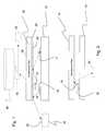
- FIG. 1is a schematic view of a first embodiment of the present invention.
- FIG. 2is another embodiment of the present invention.
- a transmitter 10can include an ultra-small resonant structure, such as any one described in U.S. patent application Ser. Nos. 11/238,991; 11/243,476; 11/243,477; 11/325,448; 11/325,432; 11/302,471; 11/325,571; 11/325,534; 11/349,963; and/or 11 / 353 , 208 (each of which is identified more particularly above).
- the resonant structures comprising the transmittercan be manufactured in accordance with any of U.S. application Ser. Nos.
- the transmitter 10can also comprise any macroscopic or microscopic light emitter, and can include even prior art LEDs, semiconductors or other light-emitting devices.
- the structuresare considered ultra-small when they embody at least one dimension that is smaller than the wavelength of visible light.
- the ultra-small structuresare also employed in a vacuum environment. Methods of evacuating the environment where the exciting and emitted encoded EMR beams move can be selected from known evacuation methods.
- the transmitter 10is mounted to a substrate 12 , is operated in association with a data source (not shown but has been described in one or more of the above referenced applications and will not be repeated herein), which may be part of the transmitter or may be separated from the transmitter.
- a data sourcenot shown but has been described in one or more of the above referenced applications and will not be repeated herein
- the kind of data transmitted, the kind of EMR produced, and the kind of structure producing the EMRare not delimiting. It matters only that in some way data are encoded into an encoded EMR beam, and for purposes of illustrating the present invention several encoded EMR beams are referenced at 14 , 16 and 18 .
- beam 14can be deflected upwardly at an angle, for example by a suitable reflector (not shown), to intersect the bottom surface 26 of an interference filter 20 , comprised of a first layer 22 formed from, for example, of a plurality of various oxide layers, including Ti, Al, Hf, or alternatively other materials with varying indices of refraction.
- filter 20may also include a second layer 24 formed of, for example, of an absorptive material such as, CdSe, that would also be either transparent or translucent.
- interference filtersare well known and the art recognizes how they are constructed and designed to control the reflection of or passage there through of selected frequencies.
- interference filtersare not needed for one skilled in the art to understand the present invention.
- the frequency of beam 14will be such that it is reflected back down to a receiver 11 on the same substrate 12 where the encoded data can be used.
- Beam 18is shown as being deflected in a direction about opposite to that of beam 14 so that beam 18 is transmitted out of the environment of substrate 12 to another device shown in phantom at 30 , and specifically to a receiver 32 thereon.
- Beam 16has a frequency which the filter 20 will allow to pass there through so that the encoded EMR beam 16 can be transmitted upwardly through filter 20 to, for example, an optical device 40 mounted above the interference filter 20 , or other receiver mounted outside the chip or the device comprising substrate 12 , which can receive and use the encoded data on beam 16 .
- beam 16can be deflected or reflected once it is beyond the bounds of interference filter 20 , as for example by a reflector 50 , that can be formed on the bottom of a device mounted above filter 22 or on another structure mounted there above, or by a magnetic or electronic deflector that could be properly mounted above filter 20 and charged to deflect the beam 16 as desired.
- beam 16be moved enough so as to be aimed as desired at another device or receiver, generally shown at 60 , where it and the encoded data thereon can be used.
- beams 14 , 16 and 18have been shown as comprising out going beams of encoded EMR, these beams could also represent incoming beams of encoded EMR or incoming EMR beams.
- an encoded EMR beam 70 emitted or produced by a transmitter 72will be reflected by interference filter 74 and the substrate 76 is comprised of a transparent or translucent material, such as, for example borosilicate glass, that permits the reflected beam 70 to pass there through and beyond substrate 76 to a receiver 80 mounted there below.
- beam 70could also be an incoming encoded EMR beam so that the data encoded thereon could be used on devices on substrate 76 , for example should 72 be a receiver instead of a transmitter.
- the substrateis comprised of silicon encoded EMR in the infer red frequency will pass there through.
Landscapes
- Physics & Mathematics (AREA)
- Optics & Photonics (AREA)
- Chemical & Material Sciences (AREA)
- Engineering & Computer Science (AREA)
- Nanotechnology (AREA)
- General Physics & Mathematics (AREA)
- Life Sciences & Earth Sciences (AREA)
- Biophysics (AREA)
- Crystallography & Structural Chemistry (AREA)
- Mechanical Light Control Or Optical Switches (AREA)
- Aerials With Secondary Devices (AREA)
- Surface Acoustic Wave Elements And Circuit Networks Thereof (AREA)
Abstract
Description
- The present invention is related to the following co-pending U.S. patent applications which are all commonly owned with the present application, the entire contents of each of which are incorporated herein by reference:
- 1. U.S. patent application Ser. No. 11/238,991, entitled “Ultra-Small Resonating Charged Particle Beam Modulator,” filed Sep. 30, 2005;
- 2. U.S. patent application Ser. No. 10/917,511, entitled “Patterning Thin Metal Film by Dry Reactive Ion Etching,” filed on Aug. 13, 2004;
- 3. U.S. application Ser. No. 11/203,407, entitled “Method Of Patterning Ultra-Small Structures,” filed on Aug. 15, 2005;
- 4. U.S. application Ser. No. 11/243,476, entitled “Structures And Methods For Coupling Energy From An Electromagnetic Wave,” filed on Oct. 5, 2005;
- 5. U.S. application Ser. No. 11/243,477, entitled “Electron beam induced resonance,” filed on Oct. 5, 2005;
- 6. U.S. application Ser. No. 11/325,448, entitled “Selectable Frequency Light Emitter from Single Metal Layer,” filed Jan. 5, 2006;
- 7. U.S. application Ser. No. 11/325,432, entitled, “Matrix Array Display,” filed Jan. 5, 2006;
- 8. U.S. application Ser. No. 11/302,471, entitled “Coupled Nano-Resonating Energy Emitting Structures,” filed Dec. 14, 2005;
- 9. U.S. application Ser. No. 11/325,571, entitled “Switching Micro-resonant Structures by Modulating a Beam of Charged Particles,” filed Jan. 5, 2006;
- 10. U.S. application Ser. No. 11/325,534, entitled “Switching Microresonant Structures Using at Least One Director,” filed Jan. 5, 2006;
- 11. U.S. application Ser. No. 11/350,812, entitled “Conductive Polymers for Electroplating,” filed Feb. 10, 2006;
- 12. U.S. application Ser. No. 11/349,963, entitled “Method and Structure for Coupling Two Microcircuits,” filed Feb. 9, 2006;
- 13. U.S. application Ser. No. 11/353,208, entitled “Electron Beam Induced Resonance,” filed Feb. 14, 2006; and
- 14. U.S. Application No. 11/______, entitled “Novel Optical Cover For Optical Chip,” filed on even date herewith [Atty. Docket 2549-0075].
- A portion of the disclosure of this patent document contains material which is subject to copyright or mask work protection. The copyright or mask work owner has no objection to the facsimile reproduction by anyone of the patent document or the patent disclosure, as it appears in the Patent and Trademark Office patent file or records, but otherwise reserves all copyright or mask work rights whatsoever.
- This relates in general to use of filtering covers for use with beams of encoded light or other forms of encoded EMR emitting structures, collectively referenced herein as encoded EMR, and specifically to covers or designed to reflect certain frequencies while permitting other frequencies to pass through the filter and directed to a receiver so that the data can be transmitted and used.
- It is not a simple task to modulate a light beam into an electron beam. Due to the size and dispersion of photons in the light beam and the size and dispersion of electrons in the electron beam the two rarely intersect, physically, even when the light beam and electron beam are directly crossed. There have been some physicists who have employed large scale lasers to intersect an electron beam and detected occasional scattered electron patterns caused by a few of the electrons in the beam physically intersecting with photons in the laser beam. But, the scale of such devices is large and their efficiency is poor.
- In the related applications described above, micro- and nano-resonant structures are described that react in now-predictable manners when an electron beam is passed in their proximity. We have seen, for example, that the very small structures described in those applications allow energy of the electron beam to be converted into the energy of electromagnetic radiation (light) when the electron beam passes nearby. When the electron beam passes near the structure, it excites synchronized oscillations of the electrons in the structure (surface plasmons). As often repeated as the many electrons in a beam pass, these surface plasmons result in reemission of detectable photons as electromagnetic radiation (EMR).
- The EMR can be modulated to encode data from a data source. The encoded EMR can then transport the data at an extremely fast data rate. Further, using resonant structures of the types described in the related applications, the transmitter can be built into a chip and used to transmit the data within a microcircuit (intra-chip) or between one or more microcircuits of one or more chips. A number of methods of encoding such data can be envisioned and is not delimiting of the inventions described herein.
- We herein disclose methods and structures for sending and receiving the encoded EMR so that the data in the encoded EMR can be used at the receiving end.
FIG. 1 is a schematic view of a first embodiment of the present invention; andFIG. 2 is another embodiment of the present invention.- With reference to
FIG. 1 , atransmitter 10 can include an ultra-small resonant structure, such as any one described in U.S. patent application Ser. Nos. 11/238,991; 11/243,476; 11/243,477; 11/325,448; 11/325,432; 11/302,471; 11/325,571; 11/325,534; 11/349,963; and/or11/353,208 (each of which is identified more particularly above). The resonant structures comprising the transmitter can be manufactured in accordance with any of U.S. application Ser. Nos. 10/917,511; 11/350,812; or 11/203,407 (each of which is identified more particularly above) or in other ways. Their sizes and dimensions can be selected in accordance with the principles described in those applications and, for the sake of brevity, will not be repeated herein. The contents of the applications described above are assumed to be known to the reader. - Although less advantageous than the ultra-small resonant structures identified in the applications described above, alternatively the
transmitter 10 can also comprise any macroscopic or microscopic light emitter, and can include even prior art LEDs, semiconductors or other light-emitting devices. As the term is used herein, the structures are considered ultra-small when they embody at least one dimension that is smaller than the wavelength of visible light. The ultra-small structures are also employed in a vacuum environment. Methods of evacuating the environment where the exciting and emitted encoded EMR beams move can be selected from known evacuation methods. - The
transmitter 10 is mounted to asubstrate 12, is operated in association with a data source (not shown but has been described in one or more of the above referenced applications and will not be repeated herein), which may be part of the transmitter or may be separated from the transmitter. For purposes of this disclosure, the kind of data transmitted, the kind of EMR produced, and the kind of structure producing the EMR are not delimiting. It matters only that in some way data are encoded into an encoded EMR beam, and for purposes of illustrating the present invention several encoded EMR beams are referenced at14,16 and18. - With reference to
FIG. 1 ,beam 14 can be deflected upwardly at an angle, for example by a suitable reflector (not shown), to intersect thebottom surface 26 of aninterference filter 20, comprised of afirst layer 22 formed from, for example, of a plurality of various oxide layers, including Ti, Al, Hf, or alternatively other materials with varying indices of refraction. As an option, filter20 may also include asecond layer 24 formed of, for example, of an absorptive material such as, CdSe, that would also be either transparent or translucent. It should be understood that interference filters are well known and the art recognizes how they are constructed and designed to control the reflection of or passage there through of selected frequencies. Consequently, further details concerning interference filters are not needed for one skilled in the art to understand the present invention. In the example as shown inFIG. 1 , asbeam 14 intersects thebottom surface 26 ofinterference filter 20 the frequency ofbeam 14 will be such that it is reflected back down to areceiver 11 on thesame substrate 12 where the encoded data can be used. Beam 18 is shown as being deflected in a direction about opposite to that ofbeam 14 so thatbeam 18 is transmitted out of the environment ofsubstrate 12 to another device shown in phantom at30, and specifically to areceiver 32 thereon.Beam 16 has a frequency which thefilter 20 will allow to pass there through so that the encodedEMR beam 16 can be transmitted upwardly throughfilter 20 to, for example, anoptical device 40 mounted above theinterference filter 20, or other receiver mounted outside the chip or thedevice comprising substrate 12, which can receive and use the encoded data onbeam 16. Alternatively,beam 16 can be deflected or reflected once it is beyond the bounds ofinterference filter 20, as for example by areflector 50, that can be formed on the bottom of a device mounted abovefilter 22 or on another structure mounted there above, or by a magnetic or electronic deflector that could be properly mounted abovefilter 20 and charged to deflect thebeam 16 as desired. Such deflectors are described in one or more of the related applications noted above so that further discussion is not needed herein. All that is required is thatbeam 16 be moved enough so as to be aimed as desired at another device or receiver, generally shown at60, where it and the encoded data thereon can be used.- It should also be understood that while the
beams - With reference to
FIG. 2 an encodedEMR beam 70 emitted or produced by atransmitter 72, comprised of ultra-small resonant structures or other energy emitting device, will be reflected byinterference filter 74 and thesubstrate 76 is comprised of a transparent or translucent material, such as, for example borosilicate glass, that permits the reflectedbeam 70 to pass there through and beyondsubstrate 76 to areceiver 80 mounted there below. Here again,beam 70 could also be an incoming encoded EMR beam so that the data encoded thereon could be used on devices onsubstrate 76, for example should72 be a receiver instead of a transmitter. As an example, where the substrate is comprised of silicon encoded EMR in the infer red frequency will pass there through. - While certain configurations of structures have been illustrated for the purposes of presenting the basic structures of the present invention, one of ordinary skill in the art will appreciate that other variations are possible which would still fall within the scope of the appended claims. While the invention has been described in connection with what is presently considered to be the most practical and preferred embodiment, it is to be understood that the invention is not to be limited to the disclosed embodiment, but on the contrary, is intended to cover various modifications and equivalent arrangements included within the spirit and scope of the appended claims.
Claims (11)
Priority Applications (3)
| Application Number | Priority Date | Filing Date | Title |
|---|---|---|---|
| US11/418,087US7443577B2 (en) | 2006-05-05 | 2006-05-05 | Reflecting filtering cover |
| PCT/US2006/022774WO2007130088A1 (en) | 2006-05-05 | 2006-06-12 | Reflecting filtering cover |
| TW095122336ATW200742877A (en) | 2006-05-05 | 2006-06-21 | Reflecting filtering cover |
Applications Claiming Priority (1)
| Application Number | Priority Date | Filing Date | Title |
|---|---|---|---|
| US11/418,087US7443577B2 (en) | 2006-05-05 | 2006-05-05 | Reflecting filtering cover |
Publications (2)
| Publication Number | Publication Date |
|---|---|
| US20070258146A1true US20070258146A1 (en) | 2007-11-08 |
| US7443577B2 US7443577B2 (en) | 2008-10-28 |
Family
ID=38660936
Family Applications (1)
| Application Number | Title | Priority Date | Filing Date |
|---|---|---|---|
| US11/418,087ActiveUS7443577B2 (en) | 2006-05-05 | 2006-05-05 | Reflecting filtering cover |
Country Status (3)
| Country | Link |
|---|---|
| US (1) | US7443577B2 (en) |
| TW (1) | TW200742877A (en) |
| WO (1) | WO2007130088A1 (en) |
Cited By (1)
| Publication number | Priority date | Publication date | Assignee | Title |
|---|---|---|---|---|
| US20150234179A1 (en)* | 2014-02-16 | 2015-08-20 | Apple Inc. | Beam scanning using an interference filter as a turning mirror |
Families Citing this family (2)
| Publication number | Priority date | Publication date | Assignee | Title |
|---|---|---|---|---|
| USD671654S1 (en)* | 2009-02-20 | 2012-11-27 | Sii Nano Technology Inc. | Compound charged particle beam device |
| WO2014093221A1 (en)* | 2012-12-10 | 2014-06-19 | Gt Crystal Systems, Llc | A mobile electronic device comprising a multilayer sapphire cover plate |
Citations (92)
| Publication number | Priority date | Publication date | Assignee | Title |
|---|---|---|---|---|
| US483021A (en)* | 1892-09-20 | Process of embedding wire-netting in glass | ||
| US1948384A (en)* | 1932-01-26 | 1934-02-20 | Research Corp | Method and apparatus for the acceleration of ions |
| US2307086A (en)* | 1941-05-07 | 1943-01-05 | Univ Leland Stanford Junior | High frequency electrical apparatus |
| US2473477A (en)* | 1946-07-24 | 1949-06-14 | Raythcon Mfg Company | Magnetic induction device |
| US2634372A (en)* | 1953-04-07 | Super high-frequency electromag | ||
| US2932798A (en)* | 1956-01-05 | 1960-04-12 | Research Corp | Imparting energy to charged particles |
| US3571642A (en)* | 1968-01-17 | 1971-03-23 | Ca Atomic Energy Ltd | Method and apparatus for interleaved charged particle acceleration |
| US3586899A (en)* | 1968-06-12 | 1971-06-22 | Ibm | Apparatus using smith-purcell effect for frequency modulation and beam deflection |
| US3761828A (en)* | 1970-12-10 | 1973-09-25 | J Pollard | Linear particle accelerator with coast through shield |
| US4282436A (en)* | 1980-06-04 | 1981-08-04 | The United States Of America As Represented By The Secretary Of The Navy | Intense ion beam generation with an inverse reflex tetrode (IRT) |
| US4727550A (en)* | 1985-09-19 | 1988-02-23 | Chang David B | Radiation source |
| US4740973A (en)* | 1984-05-21 | 1988-04-26 | Madey John M J | Free electron laser |
| US4746201A (en)* | 1967-03-06 | 1988-05-24 | Gordon Gould | Polarizing apparatus employing an optical element inclined at brewster's angle |
| US4829527A (en)* | 1984-04-23 | 1989-05-09 | The United States Of America As Represented By The Secretary Of The Army | Wideband electronic frequency tuning for orotrons |
| US5023563A (en)* | 1989-06-08 | 1991-06-11 | Hughes Aircraft Company | Upshifted free electron laser amplifier |
| US5185073A (en)* | 1988-06-21 | 1993-02-09 | International Business Machines Corporation | Method of fabricating nendritic materials |
| US5199918A (en)* | 1991-11-07 | 1993-04-06 | Microelectronics And Computer Technology Corporation | Method of forming field emitter device with diamond emission tips |
| US5302240A (en)* | 1991-01-22 | 1994-04-12 | Kabushiki Kaisha Toshiba | Method of manufacturing semiconductor device |
| US5446814A (en)* | 1993-11-05 | 1995-08-29 | Motorola | Molded reflective optical waveguide |
| US5608263A (en)* | 1994-09-06 | 1997-03-04 | The Regents Of The University Of Michigan | Micromachined self packaged circuits for high-frequency applications |
| US5668368A (en)* | 1992-02-21 | 1997-09-16 | Hitachi, Ltd. | Apparatus for suppressing electrification of sample in charged beam irradiation apparatus |
| US5705443A (en)* | 1995-05-30 | 1998-01-06 | Advanced Technology Materials, Inc. | Etching method for refractory materials |
| US5737458A (en)* | 1993-03-29 | 1998-04-07 | Martin Marietta Corporation | Optical light pipe and microwave waveguide interconnects in multichip modules formed using adaptive lithography |
| US5744919A (en)* | 1996-12-12 | 1998-04-28 | Mishin; Andrey V. | CW particle accelerator with low particle injection velocity |
| US5757009A (en)* | 1996-12-27 | 1998-05-26 | Northrop Grumman Corporation | Charged particle beam expander |
| US5767013A (en)* | 1996-08-26 | 1998-06-16 | Lg Semicon Co., Ltd. | Method for forming interconnection in semiconductor pattern device |
| US5790585A (en)* | 1996-11-12 | 1998-08-04 | The Trustees Of Dartmouth College | Grating coupling free electron laser apparatus and method |
| US5811943A (en)* | 1996-09-23 | 1998-09-22 | Schonberg Research Corporation | Hollow-beam microwave linear accelerator |
| US5889449A (en)* | 1995-12-07 | 1999-03-30 | Space Systems/Loral, Inc. | Electromagnetic transmission line elements having a boundary between materials of high and low dielectric constants |
| US5902489A (en)* | 1995-11-08 | 1999-05-11 | Hitachi, Ltd. | Particle handling method by acoustic radiation force and apparatus therefore |
| US6040625A (en)* | 1997-09-25 | 2000-03-21 | I/O Sensors, Inc. | Sensor package arrangement |
| US6060833A (en)* | 1996-10-18 | 2000-05-09 | Velazco; Jose E. | Continuous rotating-wave electron beam accelerator |
| US6080529A (en)* | 1997-12-12 | 2000-06-27 | Applied Materials, Inc. | Method of etching patterned layers useful as masking during subsequent etching or for damascene structures |
| US6195199B1 (en)* | 1997-10-27 | 2001-02-27 | Kanazawa University | Electron tube type unidirectional optical amplifier |
| US6222866B1 (en)* | 1997-01-06 | 2001-04-24 | Fuji Xerox Co., Ltd. | Surface emitting semiconductor laser, its producing method and surface emitting semiconductor laser array |
| US6338968B1 (en)* | 1998-02-02 | 2002-01-15 | Signature Bioscience, Inc. | Method and apparatus for detecting molecular binding events |
| US20020036264A1 (en)* | 2000-07-27 | 2002-03-28 | Mamoru Nakasuji | Sheet beam-type inspection apparatus |
| US6370306B1 (en)* | 1997-12-15 | 2002-04-09 | Seiko Instruments Inc. | Optical waveguide probe and its manufacturing method |
| US6373194B1 (en)* | 2000-06-01 | 2002-04-16 | Raytheon Company | Optical magnetron for high efficiency production of optical radiation |
| US20020053638A1 (en)* | 1998-07-03 | 2002-05-09 | Dieter Winkler | Apparatus and method for examing specimen with a charged particle beam |
| US6407516B1 (en)* | 2000-05-26 | 2002-06-18 | Exaconnect Inc. | Free space electron switch |
| US6441298B1 (en)* | 2000-08-15 | 2002-08-27 | Nec Research Institute, Inc | Surface-plasmon enhanced photovoltaic device |
| US20020135665A1 (en)* | 2001-03-20 | 2002-09-26 | Keith Gardner | Led print head for electrophotographic printer |
| US20030012925A1 (en)* | 2001-07-16 | 2003-01-16 | Motorola, Inc. | Process for fabricating semiconductor structures and devices utilizing the formation of a compliant substrate for materials used to form the same and including an etch stop layer used for back side processing |
| US20030016421A1 (en)* | 2000-06-01 | 2003-01-23 | Small James G. | Wireless communication system with high efficiency/high power optical source |
| US20030016412A1 (en)* | 2001-07-17 | 2003-01-23 | Alcatel | Monitoring unit for optical burst mode signals |
| US20030034535A1 (en)* | 2001-08-15 | 2003-02-20 | Motorola, Inc. | Mems devices suitable for integration with chip having integrated silicon and compound semiconductor devices, and methods for fabricating such devices |
| US6545425B2 (en)* | 2000-05-26 | 2003-04-08 | Exaconnect Corp. | Use of a free space electron switch in a telecommunications network |
| US6577040B2 (en)* | 1999-01-14 | 2003-06-10 | The Regents Of The University Of Michigan | Method and apparatus for generating a signal having at least one desired output frequency utilizing a bank of vibrating micromechanical devices |
| US6603915B2 (en)* | 2001-02-05 | 2003-08-05 | Fujitsu Limited | Interposer and method for producing a light-guiding structure |
| US20030155521A1 (en)* | 2000-02-01 | 2003-08-21 | Hans-Peter Feuerbaum | Optical column for charged particle beam device |
| US20030164947A1 (en)* | 2000-04-18 | 2003-09-04 | Matthias Vaupel | Spr sensor |
| US6624916B1 (en)* | 1997-02-11 | 2003-09-23 | Quantumbeam Limited | Signalling system |
| US20030179974A1 (en)* | 2002-03-20 | 2003-09-25 | Estes Michael J. | Surface plasmon devices |
| US20040061053A1 (en)* | 2001-02-28 | 2004-04-01 | Yoshifumi Taniguchi | Method and apparatus for measuring physical properties of micro region |
| US6738176B2 (en)* | 2002-04-30 | 2004-05-18 | Mario Rabinowitz | Dynamic multi-wavelength switching ensemble |
| US6741781B2 (en)* | 2000-09-29 | 2004-05-25 | Kabushiki Kaisha Toshiba | Optical interconnection circuit board and manufacturing method thereof |
| US20040108473A1 (en)* | 2000-06-09 | 2004-06-10 | Melnychuk Stephan T. | Extreme ultraviolet light source |
| US20040136715A1 (en)* | 2002-12-06 | 2004-07-15 | Seiko Epson Corporation | Wavelength multiplexing on-chip optical interconnection circuit, electro-optical device, and electronic apparatus |
| US20040150991A1 (en)* | 2003-01-27 | 2004-08-05 | 3M Innovative Properties Company | Phosphor based light sources utilizing total internal reflection |
| US6782205B2 (en)* | 2001-06-25 | 2004-08-24 | Silicon Light Machines | Method and apparatus for dynamic equalization in wavelength division multiplexing |
| US20040171272A1 (en)* | 2003-02-28 | 2004-09-02 | Applied Materials, Inc. | Method of etching metallic materials to form a tapered profile |
| US20050023145A1 (en)* | 2003-05-07 | 2005-02-03 | Microfabrica Inc. | Methods and apparatus for forming multi-layer structures using adhered masks |
| US20050045821A1 (en)* | 2003-04-22 | 2005-03-03 | Nobuharu Noji | Testing apparatus using charged particles and device manufacturing method using the testing apparatus |
| US20050054151A1 (en)* | 2002-01-04 | 2005-03-10 | Intersil Americas Inc. | Symmetric inducting device for an integrated circuit having a ground shield |
| US6870438B1 (en)* | 1999-11-10 | 2005-03-22 | Kyocera Corporation | Multi-layered wiring board for slot coupling a transmission line to a waveguide |
| US20050067286A1 (en)* | 2003-09-26 | 2005-03-31 | The University Of Cincinnati | Microfabricated structures and processes for manufacturing same |
| US20050082469A1 (en)* | 1997-06-19 | 2005-04-21 | European Organization For Nuclear Research | Neutron-driven element transmuter |
| US6885262B2 (en)* | 2002-11-05 | 2005-04-26 | Ube Industries, Ltd. | Band-pass filter using film bulk acoustic resonator |
| US20050092929A1 (en)* | 2003-07-08 | 2005-05-05 | Schneiker Conrad W. | Integrated sub-nanometer-scale electron beam systems |
| US20050105690A1 (en)* | 2003-11-19 | 2005-05-19 | Stanley Pau | Focusable and steerable micro-miniature x-ray apparatus |
| US6909092B2 (en)* | 2002-05-16 | 2005-06-21 | Ebara Corporation | Electron beam apparatus and device manufacturing method using same |
| US6909104B1 (en)* | 1999-05-25 | 2005-06-21 | Nawotec Gmbh | Miniaturized terahertz radiation source |
| US20050145882A1 (en)* | 2002-10-25 | 2005-07-07 | Taylor Geoff W. | Semiconductor devices employing at least one modulation doped quantum well structure and one or more etch stop layers for accurate contact formation |
| US20050162104A1 (en)* | 2000-05-26 | 2005-07-28 | Victor Michel N. | Semi-conductor interconnect using free space electron switch |
| US20060007730A1 (en)* | 2002-11-26 | 2006-01-12 | Kabushiki Kaisha Toshiba | Magnetic cell and magnetic memory |
| US20060018619A1 (en)* | 2004-06-18 | 2006-01-26 | Helffrich Jerome A | System and Method for Detection of Fiber Optic Cable Using Static and Induced Charge |
| US20060020667A1 (en)* | 2004-07-22 | 2006-01-26 | Taiwan Semiconductor Manufacturing Company, Ltd. | Electronic mail system and method for multi-geographical domains |
| US6995406B2 (en)* | 2002-06-10 | 2006-02-07 | Tsuyoshi Tojo | Multibeam semiconductor laser, semiconductor light-emitting device and semiconductor device |
| US20060035173A1 (en)* | 2004-08-13 | 2006-02-16 | Mark Davidson | Patterning thin metal films by dry reactive ion etching |
| US20060045418A1 (en)* | 2004-08-25 | 2006-03-02 | Information And Communication University Research And Industrial Cooperation Group | Optical printed circuit board and optical interconnection block using optical fiber bundle |
| US20060060782A1 (en)* | 2004-06-16 | 2006-03-23 | Anjam Khursheed | Scanning electron microscope |
| US20060062258A1 (en)* | 2004-07-02 | 2006-03-23 | Vanderbilt University | Smith-Purcell free electron laser and method of operating same |
| US20060159131A1 (en)* | 2005-01-20 | 2006-07-20 | Ansheng Liu | Digital signal regeneration, reshaping and wavelength conversion using an optical bistable silicon Raman laser |
| US20060164496A1 (en)* | 2005-01-21 | 2006-07-27 | Konica Minolta Business Technologies, Inc. | Image forming method and image forming apparatus |
| US7092588B2 (en)* | 2002-11-20 | 2006-08-15 | Seiko Epson Corporation | Optical interconnection circuit between chips, electrooptical device and electronic equipment |
| US7092603B2 (en)* | 2004-03-03 | 2006-08-15 | Fujitsu Limited | Optical bridge for chip-to-board interconnection and methods of fabrication |
| US20070003781A1 (en)* | 2005-06-30 | 2007-01-04 | De Rochemont L P | Electrical components and method of manufacture |
| US20070013765A1 (en)* | 2005-07-18 | 2007-01-18 | Eastman Kodak Company | Flexible organic laser printer |
| US7177515B2 (en)* | 2002-03-20 | 2007-02-13 | The Regents Of The University Of Colorado | Surface plasmon devices |
| US20070075264A1 (en)* | 2005-09-30 | 2007-04-05 | Virgin Islands Microsystems, Inc. | Electron beam induced resonance |
| US20070086915A1 (en)* | 2005-10-14 | 2007-04-19 | General Electric Company | Detection apparatus and associated method |
Family Cites Families (52)
| Publication number | Priority date | Publication date | Assignee | Title |
|---|---|---|---|---|
| US2431396A (en) | 1942-12-21 | 1947-11-25 | Rca Corp | Current magnitude-ratio responsive amplifier |
| US3923568A (en) | 1974-01-14 | 1975-12-02 | Int Plasma Corp | Dry plasma process for etching noble metal |
| DE2429612C2 (en) | 1974-06-20 | 1984-08-02 | Siemens AG, 1000 Berlin und 8000 München | Acousto-optical data input converter for block-organized holographic data storage and method for its control |
| US4482779A (en) | 1983-04-19 | 1984-11-13 | The United States Of America As Represented By The Administrator Of National Aeronautics And Space Administration | Inelastic tunnel diodes |
| US5163118A (en) | 1986-11-10 | 1992-11-10 | The United States Of America As Represented By The Secretary Of The Air Force | Lattice mismatched hetrostructure optical waveguide |
| US4838021A (en) | 1987-12-11 | 1989-06-13 | Hughes Aircraft Company | Electrostatic ion thruster with improved thrust modulation |
| US5157000A (en) | 1989-07-10 | 1992-10-20 | Texas Instruments Incorporated | Method for dry etching openings in integrated circuit layers |
| US5268693A (en) | 1990-08-31 | 1993-12-07 | Trustees Of Dartmouth College | Semiconductor film free electron laser |
| US5263043A (en) | 1990-08-31 | 1993-11-16 | Trustees Of Dartmouth College | Free electron laser utilizing grating coupling |
| FR2677490B1 (en) | 1991-06-07 | 1997-05-16 | Thomson Csf | SEMICONDUCTOR OPTICAL TRANSCEIVER. |
| GB9113684D0 (en)* | 1991-06-25 | 1991-08-21 | Smiths Industries Plc | Display filter arrangements |
| WO1993021663A1 (en) | 1992-04-08 | 1993-10-28 | Georgia Tech Research Corporation | Process for lift-off of thin film materials from a growth substrate |
| US5539414A (en) | 1993-09-02 | 1996-07-23 | Inmarsat | Folded dipole microstrip antenna |
| JP2921430B2 (en) | 1995-03-03 | 1999-07-19 | 双葉電子工業株式会社 | Optical writing element |
| JPH09223475A (en) | 1996-02-19 | 1997-08-26 | Nikon Corp | Electromagnetic deflector and charged particle beam transfer apparatus using the deflector |
| AU8756498A (en) | 1997-05-05 | 1998-11-27 | University Of Florida | High resolution resonance ionization imaging detector and method |
| US5821836A (en) | 1997-05-23 | 1998-10-13 | The Regents Of The University Of Michigan | Miniaturized filter assembly |
| US6297511B1 (en) | 1999-04-01 | 2001-10-02 | Raytheon Company | High frequency infrared emitter |
| JP2001273861A (en) | 2000-03-28 | 2001-10-05 | Toshiba Corp | Charged beam device and pattern tilt observation method |
| US6829286B1 (en) | 2000-05-26 | 2004-12-07 | Opticomp Corporation | Resonant cavity enhanced VCSEL/waveguide grating coupler |
| IL155030A0 (en) | 2000-09-22 | 2003-10-31 | Vermont Photonics | Apparatuses and methods for generating coherent electromagnetic laser radiation |
| AU2101902A (en) | 2000-12-01 | 2002-06-11 | Yeda Res & Dev | Device and method for the examination of samples in a non-vacuum environment using a scanning electron microscope |
| KR20020061103A (en) | 2001-01-12 | 2002-07-22 | 후루까와덴끼고오교 가부시끼가이샤 | Antenna device and terminal with the antenna device |
| US6636653B2 (en) | 2001-02-02 | 2003-10-21 | Teravicta Technologies, Inc. | Integrated optical micro-electromechanical systems and methods of fabricating and operating the same |
| WO2002077607A2 (en) | 2001-03-23 | 2002-10-03 | Vermont Photonics | Applying far infrared radiation to biological matter |
| US6912330B2 (en) | 2001-05-17 | 2005-06-28 | Sioptical Inc. | Integrated optical/electronic circuits and associated methods of simultaneous generation thereof |
| US6917727B2 (en) | 2001-09-10 | 2005-07-12 | California Institute Of Technology | Strip loaded waveguide integrated with electronics components |
| JP2003209411A (en) | 2001-10-30 | 2003-07-25 | Matsushita Electric Ind Co Ltd | High frequency module and method of manufacturing high frequency module |
| US6950220B2 (en) | 2002-03-18 | 2005-09-27 | E Ink Corporation | Electro-optic displays, and methods for driving same |
| JP2004032323A (en)* | 2002-06-25 | 2004-01-29 | Toyo Commun Equip Co Ltd | Surface mounting type piezoelectric oscillator and its manufacturing method |
| US6924920B2 (en) | 2003-05-29 | 2005-08-02 | Stanislav Zhilkov | Method of modulation and electron modulator for optical communication and data transmission |
| JP4249474B2 (en) | 2002-12-06 | 2009-04-02 | セイコーエプソン株式会社 | Wavelength multiplexing chip-to-chip optical interconnection circuit |
| US20040180244A1 (en) | 2003-01-24 | 2004-09-16 | Tour James Mitchell | Process and apparatus for microwave desorption of elements or species from carbon nanotubes |
| JP4044453B2 (en) | 2003-02-06 | 2008-02-06 | 株式会社東芝 | Quantum memory and information processing method using quantum memory |
| GB0307096D0 (en) | 2003-03-27 | 2003-04-30 | Univ Cambridge Tech | Terahertz radiation sources and methods |
| US6954515B2 (en) | 2003-04-25 | 2005-10-11 | Varian Medical Systems, Inc., | Radiation sources and radiation scanning systems with improved uniformity of radiation intensity |
| US6884335B2 (en) | 2003-05-20 | 2005-04-26 | Novellus Systems, Inc. | Electroplating using DC current interruption and variable rotation rate |
| US20050194258A1 (en) | 2003-06-27 | 2005-09-08 | Microfabrica Inc. | Electrochemical fabrication methods incorporating dielectric materials and/or using dielectric substrates |
| US6953291B2 (en) | 2003-06-30 | 2005-10-11 | Finisar Corporation | Compact package design for vertical cavity surface emitting laser array to optical fiber cable connection |
| IL157344A0 (en) | 2003-08-11 | 2004-06-20 | Opgal Ltd | Internal temperature reference source and mtf inverse filter for radiometry |
| EP1711737B1 (en) | 2004-01-28 | 2013-09-18 | Koninklijke Philips Electronics N.V. | Sealed housing unit for lighting system |
| EP1711739A4 (en) | 2004-01-28 | 2008-07-23 | Tir Technology Lp | LUMINAIRE DIRECTLY VISIBLE |
| JP4370945B2 (en) | 2004-03-11 | 2009-11-25 | ソニー株式会社 | Measuring method of dielectric constant |
| US6996303B2 (en) | 2004-03-12 | 2006-02-07 | Fujitsu Limited | Flexible optical waveguides for backplane optical interconnections |
| US7012419B2 (en) | 2004-03-26 | 2006-03-14 | Ut-Battelle, Llc | Fast Faraday cup with high bandwidth |
| JP4257741B2 (en) | 2004-04-19 | 2009-04-22 | 三菱電機株式会社 | Charged particle beam accelerator, particle beam irradiation medical system using charged particle beam accelerator, and method of operating particle beam irradiation medical system |
| US7428322B2 (en) | 2004-04-20 | 2008-09-23 | Bio-Rad Laboratories, Inc. | Imaging method and apparatus |
| US7454095B2 (en) | 2004-04-27 | 2008-11-18 | California Institute Of Technology | Integrated plasmon and dielectric waveguides |
| US7586097B2 (en) | 2006-01-05 | 2009-09-08 | Virgin Islands Microsystems, Inc. | Switching micro-resonant structures using at least one director |
| WO2006042239A2 (en) | 2004-10-06 | 2006-04-20 | The Regents Of The University Of California | Cascaded cavity silicon raman laser with electrical modulation, switching, and active mode locking capability |
| US7619373B2 (en) | 2006-01-05 | 2009-11-17 | Virgin Islands Microsystems, Inc. | Selectable frequency light emitter |
| US20070152781A1 (en) | 2006-01-05 | 2007-07-05 | Virgin Islands Microsystems, Inc. | Switching micro-resonant structures by modulating a beam of charged particles |
- 2006
- 2006-05-05USUS11/418,087patent/US7443577B2/enactiveActive
- 2006-06-12WOPCT/US2006/022774patent/WO2007130088A1/enactiveApplication Filing
- 2006-06-21TWTW095122336Apatent/TW200742877A/enunknown
Patent Citations (99)
| Publication number | Priority date | Publication date | Assignee | Title |
|---|---|---|---|---|
| US2634372A (en)* | 1953-04-07 | Super high-frequency electromag | ||
| US483021A (en)* | 1892-09-20 | Process of embedding wire-netting in glass | ||
| US1948384A (en)* | 1932-01-26 | 1934-02-20 | Research Corp | Method and apparatus for the acceleration of ions |
| US2307086A (en)* | 1941-05-07 | 1943-01-05 | Univ Leland Stanford Junior | High frequency electrical apparatus |
| US2473477A (en)* | 1946-07-24 | 1949-06-14 | Raythcon Mfg Company | Magnetic induction device |
| US2932798A (en)* | 1956-01-05 | 1960-04-12 | Research Corp | Imparting energy to charged particles |
| US4746201A (en)* | 1967-03-06 | 1988-05-24 | Gordon Gould | Polarizing apparatus employing an optical element inclined at brewster's angle |
| US3571642A (en)* | 1968-01-17 | 1971-03-23 | Ca Atomic Energy Ltd | Method and apparatus for interleaved charged particle acceleration |
| US3586899A (en)* | 1968-06-12 | 1971-06-22 | Ibm | Apparatus using smith-purcell effect for frequency modulation and beam deflection |
| US3761828A (en)* | 1970-12-10 | 1973-09-25 | J Pollard | Linear particle accelerator with coast through shield |
| US4282436A (en)* | 1980-06-04 | 1981-08-04 | The United States Of America As Represented By The Secretary Of The Navy | Intense ion beam generation with an inverse reflex tetrode (IRT) |
| US4829527A (en)* | 1984-04-23 | 1989-05-09 | The United States Of America As Represented By The Secretary Of The Army | Wideband electronic frequency tuning for orotrons |
| US4740973A (en)* | 1984-05-21 | 1988-04-26 | Madey John M J | Free electron laser |
| US4727550A (en)* | 1985-09-19 | 1988-02-23 | Chang David B | Radiation source |
| US5185073A (en)* | 1988-06-21 | 1993-02-09 | International Business Machines Corporation | Method of fabricating nendritic materials |
| US5023563A (en)* | 1989-06-08 | 1991-06-11 | Hughes Aircraft Company | Upshifted free electron laser amplifier |
| US5302240A (en)* | 1991-01-22 | 1994-04-12 | Kabushiki Kaisha Toshiba | Method of manufacturing semiconductor device |
| US5199918A (en)* | 1991-11-07 | 1993-04-06 | Microelectronics And Computer Technology Corporation | Method of forming field emitter device with diamond emission tips |
| US5668368A (en)* | 1992-02-21 | 1997-09-16 | Hitachi, Ltd. | Apparatus for suppressing electrification of sample in charged beam irradiation apparatus |
| US5737458A (en)* | 1993-03-29 | 1998-04-07 | Martin Marietta Corporation | Optical light pipe and microwave waveguide interconnects in multichip modules formed using adaptive lithography |
| US5446814A (en)* | 1993-11-05 | 1995-08-29 | Motorola | Molded reflective optical waveguide |
| US5608263A (en)* | 1994-09-06 | 1997-03-04 | The Regents Of The University Of Michigan | Micromachined self packaged circuits for high-frequency applications |
| US5705443A (en)* | 1995-05-30 | 1998-01-06 | Advanced Technology Materials, Inc. | Etching method for refractory materials |
| US5902489A (en)* | 1995-11-08 | 1999-05-11 | Hitachi, Ltd. | Particle handling method by acoustic radiation force and apparatus therefore |
| US5889449A (en)* | 1995-12-07 | 1999-03-30 | Space Systems/Loral, Inc. | Electromagnetic transmission line elements having a boundary between materials of high and low dielectric constants |
| US20020027481A1 (en)* | 1995-12-07 | 2002-03-07 | Fiedziuszko Slawomir J. | Electromagnetic transmission line elements having a boundary between materials of high and low dielectric constants |
| US6281769B1 (en)* | 1995-12-07 | 2001-08-28 | Space Systems/Loral Inc. | Electromagnetic transmission line elements having a boundary between materials of high and low dielectric constants |
| US5767013A (en)* | 1996-08-26 | 1998-06-16 | Lg Semicon Co., Ltd. | Method for forming interconnection in semiconductor pattern device |
| US5811943A (en)* | 1996-09-23 | 1998-09-22 | Schonberg Research Corporation | Hollow-beam microwave linear accelerator |
| US6060833A (en)* | 1996-10-18 | 2000-05-09 | Velazco; Jose E. | Continuous rotating-wave electron beam accelerator |
| US5790585A (en)* | 1996-11-12 | 1998-08-04 | The Trustees Of Dartmouth College | Grating coupling free electron laser apparatus and method |
| US5744919A (en)* | 1996-12-12 | 1998-04-28 | Mishin; Andrey V. | CW particle accelerator with low particle injection velocity |
| US5757009A (en)* | 1996-12-27 | 1998-05-26 | Northrop Grumman Corporation | Charged particle beam expander |
| US6222866B1 (en)* | 1997-01-06 | 2001-04-24 | Fuji Xerox Co., Ltd. | Surface emitting semiconductor laser, its producing method and surface emitting semiconductor laser array |
| US6624916B1 (en)* | 1997-02-11 | 2003-09-23 | Quantumbeam Limited | Signalling system |
| US20050082469A1 (en)* | 1997-06-19 | 2005-04-21 | European Organization For Nuclear Research | Neutron-driven element transmuter |
| US6040625A (en)* | 1997-09-25 | 2000-03-21 | I/O Sensors, Inc. | Sensor package arrangement |
| US6195199B1 (en)* | 1997-10-27 | 2001-02-27 | Kanazawa University | Electron tube type unidirectional optical amplifier |
| US6080529A (en)* | 1997-12-12 | 2000-06-27 | Applied Materials, Inc. | Method of etching patterned layers useful as masking during subsequent etching or for damascene structures |
| US6370306B1 (en)* | 1997-12-15 | 2002-04-09 | Seiko Instruments Inc. | Optical waveguide probe and its manufacturing method |
| US6338968B1 (en)* | 1998-02-02 | 2002-01-15 | Signature Bioscience, Inc. | Method and apparatus for detecting molecular binding events |
| US20020009723A1 (en)* | 1998-02-02 | 2002-01-24 | John Hefti | Resonant bio-assay device and test system for detecting molecular binding events |
| US6376258B2 (en)* | 1998-02-02 | 2002-04-23 | Signature Bioscience, Inc. | Resonant bio-assay device and test system for detecting molecular binding events |
| US20020053638A1 (en)* | 1998-07-03 | 2002-05-09 | Dieter Winkler | Apparatus and method for examing specimen with a charged particle beam |
| US6577040B2 (en)* | 1999-01-14 | 2003-06-10 | The Regents Of The University Of Michigan | Method and apparatus for generating a signal having at least one desired output frequency utilizing a bank of vibrating micromechanical devices |
| US6909104B1 (en)* | 1999-05-25 | 2005-06-21 | Nawotec Gmbh | Miniaturized terahertz radiation source |
| US6870438B1 (en)* | 1999-11-10 | 2005-03-22 | Kyocera Corporation | Multi-layered wiring board for slot coupling a transmission line to a waveguide |
| US20030155521A1 (en)* | 2000-02-01 | 2003-08-21 | Hans-Peter Feuerbaum | Optical column for charged particle beam device |
| US20030164947A1 (en)* | 2000-04-18 | 2003-09-04 | Matthias Vaupel | Spr sensor |
| US20050162104A1 (en)* | 2000-05-26 | 2005-07-28 | Victor Michel N. | Semi-conductor interconnect using free space electron switch |
| US6407516B1 (en)* | 2000-05-26 | 2002-06-18 | Exaconnect Inc. | Free space electron switch |
| US6545425B2 (en)* | 2000-05-26 | 2003-04-08 | Exaconnect Corp. | Use of a free space electron switch in a telecommunications network |
| US20030016421A1 (en)* | 2000-06-01 | 2003-01-23 | Small James G. | Wireless communication system with high efficiency/high power optical source |
| US6373194B1 (en)* | 2000-06-01 | 2002-04-16 | Raytheon Company | Optical magnetron for high efficiency production of optical radiation |
| US6504303B2 (en)* | 2000-06-01 | 2003-01-07 | Raytheon Company | Optical magnetron for high efficiency production of optical radiation, and 1/2λ induced pi-mode operation |
| US20040108473A1 (en)* | 2000-06-09 | 2004-06-10 | Melnychuk Stephan T. | Extreme ultraviolet light source |
| US20020036264A1 (en)* | 2000-07-27 | 2002-03-28 | Mamoru Nakasuji | Sheet beam-type inspection apparatus |
| US6441298B1 (en)* | 2000-08-15 | 2002-08-27 | Nec Research Institute, Inc | Surface-plasmon enhanced photovoltaic device |
| US6741781B2 (en)* | 2000-09-29 | 2004-05-25 | Kabushiki Kaisha Toshiba | Optical interconnection circuit board and manufacturing method thereof |
| US6603915B2 (en)* | 2001-02-05 | 2003-08-05 | Fujitsu Limited | Interposer and method for producing a light-guiding structure |
| US20040061053A1 (en)* | 2001-02-28 | 2004-04-01 | Yoshifumi Taniguchi | Method and apparatus for measuring physical properties of micro region |
| US20020135665A1 (en)* | 2001-03-20 | 2002-09-26 | Keith Gardner | Led print head for electrophotographic printer |
| US6782205B2 (en)* | 2001-06-25 | 2004-08-24 | Silicon Light Machines | Method and apparatus for dynamic equalization in wavelength division multiplexing |
| US20030012925A1 (en)* | 2001-07-16 | 2003-01-16 | Motorola, Inc. | Process for fabricating semiconductor structures and devices utilizing the formation of a compliant substrate for materials used to form the same and including an etch stop layer used for back side processing |
| US20030016412A1 (en)* | 2001-07-17 | 2003-01-23 | Alcatel | Monitoring unit for optical burst mode signals |
| US20030034535A1 (en)* | 2001-08-15 | 2003-02-20 | Motorola, Inc. | Mems devices suitable for integration with chip having integrated silicon and compound semiconductor devices, and methods for fabricating such devices |
| US20050054151A1 (en)* | 2002-01-04 | 2005-03-10 | Intersil Americas Inc. | Symmetric inducting device for an integrated circuit having a ground shield |
| US7010183B2 (en)* | 2002-03-20 | 2006-03-07 | The Regents Of The University Of Colorado | Surface plasmon devices |
| US7177515B2 (en)* | 2002-03-20 | 2007-02-13 | The Regents Of The University Of Colorado | Surface plasmon devices |
| US20030179974A1 (en)* | 2002-03-20 | 2003-09-25 | Estes Michael J. | Surface plasmon devices |
| US20070116420A1 (en)* | 2002-03-20 | 2007-05-24 | Estes Michael J | Surface Plasmon Devices |
| US6738176B2 (en)* | 2002-04-30 | 2004-05-18 | Mario Rabinowitz | Dynamic multi-wavelength switching ensemble |
| US6909092B2 (en)* | 2002-05-16 | 2005-06-21 | Ebara Corporation | Electron beam apparatus and device manufacturing method using same |
| US6995406B2 (en)* | 2002-06-10 | 2006-02-07 | Tsuyoshi Tojo | Multibeam semiconductor laser, semiconductor light-emitting device and semiconductor device |
| US20050145882A1 (en)* | 2002-10-25 | 2005-07-07 | Taylor Geoff W. | Semiconductor devices employing at least one modulation doped quantum well structure and one or more etch stop layers for accurate contact formation |
| US6885262B2 (en)* | 2002-11-05 | 2005-04-26 | Ube Industries, Ltd. | Band-pass filter using film bulk acoustic resonator |
| US7092588B2 (en)* | 2002-11-20 | 2006-08-15 | Seiko Epson Corporation | Optical interconnection circuit between chips, electrooptical device and electronic equipment |
| US20060007730A1 (en)* | 2002-11-26 | 2006-01-12 | Kabushiki Kaisha Toshiba | Magnetic cell and magnetic memory |
| US20040136715A1 (en)* | 2002-12-06 | 2004-07-15 | Seiko Epson Corporation | Wavelength multiplexing on-chip optical interconnection circuit, electro-optical device, and electronic apparatus |
| US20040150991A1 (en)* | 2003-01-27 | 2004-08-05 | 3M Innovative Properties Company | Phosphor based light sources utilizing total internal reflection |
| US20040171272A1 (en)* | 2003-02-28 | 2004-09-02 | Applied Materials, Inc. | Method of etching metallic materials to form a tapered profile |
| US20050045821A1 (en)* | 2003-04-22 | 2005-03-03 | Nobuharu Noji | Testing apparatus using charged particles and device manufacturing method using the testing apparatus |
| US20050023145A1 (en)* | 2003-05-07 | 2005-02-03 | Microfabrica Inc. | Methods and apparatus for forming multi-layer structures using adhered masks |
| US20050092929A1 (en)* | 2003-07-08 | 2005-05-05 | Schneiker Conrad W. | Integrated sub-nanometer-scale electron beam systems |
| US20050067286A1 (en)* | 2003-09-26 | 2005-03-31 | The University Of Cincinnati | Microfabricated structures and processes for manufacturing same |
| US20050105690A1 (en)* | 2003-11-19 | 2005-05-19 | Stanley Pau | Focusable and steerable micro-miniature x-ray apparatus |
| US7092603B2 (en)* | 2004-03-03 | 2006-08-15 | Fujitsu Limited | Optical bridge for chip-to-board interconnection and methods of fabrication |
| US20060060782A1 (en)* | 2004-06-16 | 2006-03-23 | Anjam Khursheed | Scanning electron microscope |
| US20060018619A1 (en)* | 2004-06-18 | 2006-01-26 | Helffrich Jerome A | System and Method for Detection of Fiber Optic Cable Using Static and Induced Charge |
| US20060062258A1 (en)* | 2004-07-02 | 2006-03-23 | Vanderbilt University | Smith-Purcell free electron laser and method of operating same |
| US20060020667A1 (en)* | 2004-07-22 | 2006-01-26 | Taiwan Semiconductor Manufacturing Company, Ltd. | Electronic mail system and method for multi-geographical domains |
| US20060035173A1 (en)* | 2004-08-13 | 2006-02-16 | Mark Davidson | Patterning thin metal films by dry reactive ion etching |
| US20060045418A1 (en)* | 2004-08-25 | 2006-03-02 | Information And Communication University Research And Industrial Cooperation Group | Optical printed circuit board and optical interconnection block using optical fiber bundle |
| US20060159131A1 (en)* | 2005-01-20 | 2006-07-20 | Ansheng Liu | Digital signal regeneration, reshaping and wavelength conversion using an optical bistable silicon Raman laser |
| US20060164496A1 (en)* | 2005-01-21 | 2006-07-27 | Konica Minolta Business Technologies, Inc. | Image forming method and image forming apparatus |
| US20070003781A1 (en)* | 2005-06-30 | 2007-01-04 | De Rochemont L P | Electrical components and method of manufacture |
| US20070013765A1 (en)* | 2005-07-18 | 2007-01-18 | Eastman Kodak Company | Flexible organic laser printer |
| US20070075264A1 (en)* | 2005-09-30 | 2007-04-05 | Virgin Islands Microsystems, Inc. | Electron beam induced resonance |
| US20070086915A1 (en)* | 2005-10-14 | 2007-04-19 | General Electric Company | Detection apparatus and associated method |
Cited By (2)
| Publication number | Priority date | Publication date | Assignee | Title |
|---|---|---|---|---|
| US20150234179A1 (en)* | 2014-02-16 | 2015-08-20 | Apple Inc. | Beam scanning using an interference filter as a turning mirror |
| US9523850B2 (en)* | 2014-02-16 | 2016-12-20 | Apple Inc. | Beam scanning using an interference filter as a turning mirror |
Also Published As
| Publication number | Publication date |
|---|---|
| WO2007130088A1 (en) | 2007-11-15 |
| US7443577B2 (en) | 2008-10-28 |
| TW200742877A (en) | 2007-11-16 |
Similar Documents
| Publication | Publication Date | Title |
|---|---|---|
| US7554083B2 (en) | Integration of electromagnetic detector on integrated chip | |
| US7342441B2 (en) | Heterodyne receiver array using resonant structures | |
| US6586775B2 (en) | Light-emitting device and a display apparatus having a light-emitting device | |
| US20070258720A1 (en) | Inter-chip optical communication | |
| US9461202B2 (en) | High-efficiency light-emitting device and manufacturing method thereof | |
| JP5664657B2 (en) | Optical element, light source, and projection display device | |
| JP4871994B2 (en) | Nanoparticles coupled to a waveguide | |
| CN101939849A (en) | Systems and methods for emitter layer shaping | |
| US7443577B2 (en) | Reflecting filtering cover | |
| TWI741661B (en) | Speckle reduction in vcsel arrays | |
| TW200425778A (en) | Transparent substrate for area light emitting device, a method for producing transparent substrate, and area light emitting device and liquid crystal display device | |
| US7911395B2 (en) | Optically driven antenna | |
| US7579609B2 (en) | Coupling light of light emitting resonator to waveguide | |
| US20070257199A1 (en) | Heterodyne receiver using resonant structures | |
| US8188431B2 (en) | Integration of vacuum microelectronic device with integrated circuit | |
| US7990336B2 (en) | Microwave coupled excitation of solid state resonant arrays | |
| US20070257273A1 (en) | Novel optical cover for optical chip | |
| US7583370B2 (en) | Resonant structures and methods for encoding signals into surface plasmons | |
| US20070258675A1 (en) | Multiplexed optical communication between chips on a multi-chip module | |
| US7679067B2 (en) | Receiver array using shared electron beam | |
| US7558490B2 (en) | Resonant detector for optical signals | |
| US10211428B2 (en) | Metal-based optical device enabling efficient light generation from emitters on a high-index absorbing substrate | |
| EP1098375A1 (en) | Optical filter and Resonant Cavity LED comprising the said optical filter | |
| JP6917626B2 (en) | Laminated transparent phosphor and lighting equipment | |
| US7723698B2 (en) | Top metal layer shield for ultra-small resonant structures |
Legal Events
| Date | Code | Title | Description |
|---|---|---|---|
| AS | Assignment | Owner name:VIRGIN ISLANDS MICROSYSTEMS, INC., VIRGIN ISLANDS, Free format text:ASSIGNMENT OF ASSIGNORS INTEREST;ASSIGNORS:GORRELL, JONATHAN;DAVIDSON, MARK;REEL/FRAME:017803/0128 Effective date:20060523 | |
| STCF | Information on status: patent grant | Free format text:PATENTED CASE | |
| AS | Assignment | Owner name:V.I. FOUNDERS, LLC, VIRGIN ISLANDS, U.S. Free format text:SECURITY AGREEMENT;ASSIGNOR:APPLIED PLASMONICS, INC.;REEL/FRAME:023594/0877 Effective date:20091009 | |
| FEPP | Fee payment procedure | Free format text:PAYOR NUMBER ASSIGNED (ORIGINAL EVENT CODE: ASPN); ENTITY STATUS OF PATENT OWNER: SMALL ENTITY | |
| AS | Assignment | Owner name:V.I. FOUNDERS, LLC, VIRGIN ISLANDS, U.S. Free format text:SECURITY AGREEMENT;ASSIGNOR:ADVANCED PLASMONICS, INC.;REEL/FRAME:028022/0961 Effective date:20111104 | |
| FPAY | Fee payment | Year of fee payment:4 | |
| AS | Assignment | Owner name:APPLIED PLASMONICS, INC., VIRGIN ISLANDS, U.S. Free format text:NUNC PRO TUNC ASSIGNMENT;ASSIGNOR:VIRGIN ISLAND MICROSYSTEMS, INC.;REEL/FRAME:029067/0657 Effective date:20120921 | |
| AS | Assignment | Owner name:ADVANCED PLASMONICS, INC., FLORIDA Free format text:NUNC PRO TUNC ASSIGNMENT;ASSIGNOR:APPLIED PLASMONICS, INC.;REEL/FRAME:029095/0525 Effective date:20120921 | |
| REMI | Maintenance fee reminder mailed | ||
| FPAY | Fee payment | Year of fee payment:8 | |
| SULP | Surcharge for late payment | Year of fee payment:7 | |
| AS | Assignment | Owner name:V.I. FOUNDERS, LLC, VIRGIN ISLANDS, U.S. Free format text:CORRECTIVE ASSIGNMENT TO CORRECT THE ASSIGNMENT PREVIOUSLY RECORDED AT REEL: 028022 FRAME: 0961. ASSIGNOR(S) HEREBY CONFIRMS THE CORRECTIVE ASSIGNMENT TO CORRECT THE #27 IN SCHEDULE I OF ASSIGNMENT SHOULD BE: TRANSMISSION OF DATA BETWEEN MICROCHIPS USING A PARTICLE BEAM, PAT. NO 7569836.;ASSIGNOR:ADVANCED PLASMONICS, INC.;REEL/FRAME:044945/0570 Effective date:20111104 | |
| AS | Assignment | Owner name:V.I. FOUNDERS, LLC, VIRGIN ISLANDS, U.S. Free format text:CORRECTIVE ASSIGNMENT TO CORRECT THE TO REMOVE PATENT 7,559,836 WHICH WAS ERRONEOUSLY CITED IN LINE 27 OF SCHEDULE I AND NEEDS TO BE REMOVED AS FILED ON 4/10/2012. PREVIOUSLY RECORDED ON REEL 028022 FRAME 0961. ASSIGNOR(S) HEREBY CONFIRMS THE SECURITY AGREEMENT;ASSIGNOR:ADVANCED PLASMONICS, INC.;REEL/FRAME:046011/0827 Effective date:20111104 | |
| FEPP | Fee payment procedure | Free format text:MAINTENANCE FEE REMINDER MAILED (ORIGINAL EVENT CODE: REM.); ENTITY STATUS OF PATENT OWNER: SMALL ENTITY | |
| FEPP | Fee payment procedure | Free format text:11.5 YR SURCHARGE- LATE PMT W/IN 6 MO, SMALL ENTITY (ORIGINAL EVENT CODE: M2556); ENTITY STATUS OF PATENT OWNER: SMALL ENTITY | |
| MAFP | Maintenance fee payment | Free format text:PAYMENT OF MAINTENANCE FEE, 12TH YR, SMALL ENTITY (ORIGINAL EVENT CODE: M2553); ENTITY STATUS OF PATENT OWNER: SMALL ENTITY Year of fee payment:12 |