US20070256472A1 - SEM test apparatus - Google Patents
SEM test apparatusDownload PDFInfo
- Publication number
- US20070256472A1 US20070256472A1US11/418,081US41808106AUS2007256472A1US 20070256472 A1US20070256472 A1US 20070256472A1US 41808106 AUS41808106 AUS 41808106AUS 2007256472 A1US2007256472 A1US 2007256472A1
- Authority
- US
- United States
- Prior art keywords
- test apparatus
- array
- ultra
- stage
- sem
- Prior art date
- Legal status (The legal status is an assumption and is not a legal conclusion. Google has not performed a legal analysis and makes no representation as to the accuracy of the status listed.)
- Granted
Links
- 238000012360testing methodMethods0.000titleclaimsabstractdescription27
- 239000002245particleSubstances0.000claimsabstractdescription19
- 239000000758substrateSubstances0.000claimsdescription23
- 238000003491arrayMethods0.000claimsdescription6
- 230000003287optical effectEffects0.000claimsdescription4
- 238000010894electron beam technologyMethods0.000abstractdescription3
- 230000005670electromagnetic radiationEffects0.000description10
- 239000000463materialSubstances0.000description9
- 238000000034methodMethods0.000description7
- 229910052751metalInorganic materials0.000description4
- 239000002184metalSubstances0.000description4
- 238000013459approachMethods0.000description3
- 238000012986modificationMethods0.000description3
- 230000004048modificationEffects0.000description3
- RYGMFSIKBFXOCR-UHFFFAOYSA-NCopperChemical compound[Cu]RYGMFSIKBFXOCR-UHFFFAOYSA-N0.000description2
- BQCADISMDOOEFD-UHFFFAOYSA-NSilverChemical compound[Ag]BQCADISMDOOEFD-UHFFFAOYSA-N0.000description2
- 230000015572biosynthetic processEffects0.000description2
- 230000008859changeEffects0.000description2
- 229910052802copperInorganic materials0.000description2
- 239000010949copperSubstances0.000description2
- 230000005284excitationEffects0.000description2
- PCHJSUWPFVWCPO-UHFFFAOYSA-NgoldChemical compound[Au]PCHJSUWPFVWCPO-UHFFFAOYSA-N0.000description2
- 229910052737goldInorganic materials0.000description2
- 239000010931goldSubstances0.000description2
- 150000002500ionsChemical class0.000description2
- 150000002739metalsChemical class0.000description2
- 239000002105nanoparticleSubstances0.000description2
- 238000000059patterningMethods0.000description2
- BASFCYQUMIYNBI-UHFFFAOYSA-NplatinumChemical compound[Pt]BASFCYQUMIYNBI-UHFFFAOYSA-N0.000description2
- 230000008569processEffects0.000description2
- 229910052709silverInorganic materials0.000description2
- 239000004332silverSubstances0.000description2
- 238000001228spectrumMethods0.000description2
- OKTJSMMVPCPJKN-UHFFFAOYSA-NCarbonChemical compound[C]OKTJSMMVPCPJKN-UHFFFAOYSA-N0.000description1
- 229910045601alloyInorganic materials0.000description1
- 239000000956alloySubstances0.000description1
- 229910052782aluminiumInorganic materials0.000description1
- XAGFODPZIPBFFR-UHFFFAOYSA-NaluminiumChemical compound[Al]XAGFODPZIPBFFR-UHFFFAOYSA-N0.000description1
- 239000002041carbon nanotubeSubstances0.000description1
- 229910021393carbon nanotubeInorganic materials0.000description1
- 238000004590computer programMethods0.000description1
- 229920001940conductive polymerPolymers0.000description1
- 230000008878couplingEffects0.000description1
- 238000010168coupling processMethods0.000description1
- 238000005859coupling reactionMethods0.000description1
- 238000000151depositionMethods0.000description1
- 238000013461designMethods0.000description1
- 230000000694effectsEffects0.000description1
- 238000009713electroplatingMethods0.000description1
- 230000007613environmental effectEffects0.000description1
- 238000005530etchingMethods0.000description1
- 230000003993interactionEffects0.000description1
- 238000004519manufacturing processMethods0.000description1
- 238000001020plasma etchingMethods0.000description1
- 238000007747platingMethods0.000description1
- 229910052697platinumInorganic materials0.000description1
- 239000000126substanceSubstances0.000description1
- 239000002887superconductorSubstances0.000description1
- 238000013519translationMethods0.000description1
- WFKWXMTUELFFGS-UHFFFAOYSA-NtungstenChemical compound[W]WFKWXMTUELFFGS-UHFFFAOYSA-N0.000description1
- 229910052721tungstenInorganic materials0.000description1
- 239000010937tungstenSubstances0.000description1
Images


Classifications
- G—PHYSICS
- G01—MEASURING; TESTING
- G01N—INVESTIGATING OR ANALYSING MATERIALS BY DETERMINING THEIR CHEMICAL OR PHYSICAL PROPERTIES
- G01N23/00—Investigating or analysing materials by the use of wave or particle radiation, e.g. X-rays or neutrons, not covered by groups G01N3/00 – G01N17/00, G01N21/00 or G01N22/00
- G01N23/22—Investigating or analysing materials by the use of wave or particle radiation, e.g. X-rays or neutrons, not covered by groups G01N3/00 – G01N17/00, G01N21/00 or G01N22/00 by measuring secondary emission from the material
- G01N23/225—Investigating or analysing materials by the use of wave or particle radiation, e.g. X-rays or neutrons, not covered by groups G01N3/00 – G01N17/00, G01N21/00 or G01N22/00 by measuring secondary emission from the material using electron or ion
- H—ELECTRICITY
- H01—ELECTRIC ELEMENTS
- H01J—ELECTRIC DISCHARGE TUBES OR DISCHARGE LAMPS
- H01J25/00—Transit-time tubes, e.g. klystrons, travelling-wave tubes, magnetrons
- H—ELECTRICITY
- H01—ELECTRIC ELEMENTS
- H01J—ELECTRIC DISCHARGE TUBES OR DISCHARGE LAMPS
- H01J2237/00—Discharge tubes exposing object to beam, e.g. for analysis treatment, etching, imaging
- H01J2237/26—Electron or ion microscopes
- H01J2237/28—Scanning microscopes
- H01J2237/2813—Scanning microscopes characterised by the application
Definitions
- the present inventionis related to the following co-pending U.S. patent applications: (1) U.S. patent application Ser. No. 11/238,991 [atty. docket 2549-0003], filed Sep. 30, 2005, entitled “Ultra-Small Resonating Charged Particle Beam Modulator”; (2) U.S. patent application Ser. No. 10/917,511 [atty. docket 2549-0002], filed on Aug. 13, 2004, entitled “Patterning Thin Metal Film by Dry Reactive Ion Etching”; (3) U.S. application Ser. No. 11/203,407 [atty. docket 2549-0040], filed on Aug. 15, 2005, entitled “Method Of Patterning Ultra-Small Structures”; (4) U.S.
- This disclosurerelates to the use and testing of ultra-small resonant structures, and arrays formed there from, together with the formation of associated structures located adjacent such ultra-small resonant structures, and specifically an approach for checking the operation of ultra-small resonant structures as they are excited by beams of charged particles directed there past within, for example, a high resolution, scanning electron microscope, a high resolution, field emission scanning electron microscope (FE-SEM) or an environmental scanning electron microscope (ESEM) (collectively referred to herein as an “SEM”), and light or other electromagnetic radiation (EMR) produced by the excited ultra-small resonant structures.
- FE-SEMfield emission scanning electron microscope
- ESEMenvironmental scanning electron microscope
- Ultra-small structuresencompass a range of structure sizes sometimes described as micro- or nano-sized. Objects with dimensions measured in ones, tens or hundreds of microns are described as micro-sized. Objects with dimensions measured in ones, tens or hundreds of nanometers or less are commonly designated nano-sized. Ultra-small hereinafter refers to structures and features ranging in size from hundreds of microns in size to ones of nanometers in size.
- the devices of the present inventionproduce electromagnetic radiation (EMR), light or energy in a variety of spectrums by the excitation of ultra-small resonant structures.
- EMRelectromagnetic radiation
- the resonant excitation in a device according to the inventionis induced by electromagnetic interaction which is caused, e.g., by the passing of a charged particle beam in close proximity to the device.
- the charged particle beamcan include ions (positive or negative), electrons, protons and the like.
- the beammay be produced by any source, including, e.g., without limitation an ion gun, a tungsten filament, a cathode, a planar vacuum triode, an electron-impact ionizer, a laser ionizer, a chemical ionizer, a thermal ionizer, an ion-impact ionizer. It is desirable to be able to quickly test the operation of ultra-small resonant structures formed on a substrate, to test such ultra-small resonant structures in a quick yet precise manner, and in apparatus that requires minimal set up. It is equally important that alignment of the beam of charged particles and the ultra-small resonant structures to be excited can be accomplished very precisely and under controlled and repeatable conditions.
- ultra-small resonant structureshall mean any structure of any material, type or microscopic size that by its characteristics causes electrons to resonate at a frequency in excess of the microwave frequency.
- ultra-smallwithin the phrase “ultra-small resonant structure” shall mean microscopic structural dimensions and shall include so-called “micro” structures, “nano” structures, or any other very small structures that will produce resonance at frequencies in excess of microwave frequencies.
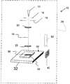
- FIG. 1is a diagrammatic showing of a scanning electron microscope (SEM) based test apparatus
- FIG. 2is a diagrammatic showing of an SEM where a nano-stage has been mounted and moved to orient an array of ultra-small resonant structures relative to a beam of charged particles within the SEM;
- FIG. 3shows an enlarged view of the nano-stage and its positions of movement
- FIG. 4shows another approach for detecting the EMR produced by the ultra-small resonant structures.
- Ultra-small resonating structurescan be constructed with many types of materials. Examples of suitable fabrication materials include silver, copper, gold, and other high conductivity metals, and high temperature superconducting materials. The material may be opaque or semi-transparent. In the above-identified patent applications, ultra-small structures for producing electromagnetic radiation are disclosed, and methods of making the same.
- the resonant structures of the present inventionare made from at least one layer of metal (e.g., silver, gold, aluminum, platinum or copper or alloys made with such metals); however, multiple layers and non-metallic structures (e.g., carbon nanotubes and high temperature superconductors) can be utilized, as long as the structures are excited by the passage of a charged particle beam.
- the materials making up the resonant structuresmay be deposited on a substrate and then etched, electroplated, or otherwise processed to create a number of individual resonant elements.
- the materialneed not even be a contiguous layer, but can be a series of resonant elements individually present on a substrate.
- the materials making up the resonant elementscan be produced by a variety of methods, such as by pulsed-plating, depositing or etching. Preferred methods for doing so are described in co-pending U.S. application Ser. Nos. 10/917,571 and Ser. No. 11/203,407, both of which were previously referenced above and incorporated herein by reference.
- a diagrammatic representation of a scanning electron microscope (SEM) 10is set forth and includes a source 12 of a beam 14 of charged particles. Such a beam is usually focused or controlled to confine it by a suitable beam control 16 , such as Wehnelt, or other similar beam control device that is part of the SEM, and an anode 18 .
- An SEMwill also include one or more condenser lenses 20 and an objective lens 22 to direct the beam within the microscope. Since SEM's are well known to those skilled in the art, further details thereof are not needed nor provided herein.
- FIG. 1also shows in phantom an outer housing 24 since the testing process will, as with SEM use, take place under vacuum conditions.
- the housingwill differ with each model, type and manufacturer of SEM equipment thus requiring the housing to be represented only. This is not to be taken as a limiting factor with the present invention.
- FIG. 1also shows a stage to hold the sample being tested, and in particular a nano-stage for holding and positioning the array of ultra-small resonant structures.
- the nano-stage 30includes a main stage 32 on which the substrate 34 is mounted and on which has been formed a light emitting device array 36 .
- the light emitting device array 36 of ultra-small resonant structuresshould contain two or more ultra-small resonant structures 38 , as shown in FIG. 3 , it can be formed from a plurality of ultra-small resonant structures.
- the light emitting device array 36could be comprised of several arrays of ultra-small resonant structures, and the substrate 36 could be a portion of a chip, an entire chip, or a portion of a substrate being used in the formation of ultra-small resonant structures that has been cut from a larger substrate.
- the stagehas been placed in the SEM but has not yet been oriented.
- FIG. 2shows the nano-stage 30 as having been booth rotated and tilted to orient the array 36 to be aligned with and preferably parallel with the beam 14 .
- Nano-stage 30has been designed to be movable in multiple directions, including at least the X, Y and Z directions, as shown by that symbol in FIG. 2 .
- the nano-stage 30is also tiltable and rotatable in multiple directions and degrees. Movement in the X direction in an SEM is normally in a range of about 0 to 100 mm, but only movement in the range of 0-100 nm is required in most instances for nano-stage 30 .
- Movement in the Y and Z directionsare usually in the range of 0-80 mm and 0-50 mm, respectively, but with the nano-stage 30 , Y and Z movement in the ranges of 0-80 nm and 0-50 nm, respectively, should be sufficient. Tilting can be in the range of about ⁇ 10° and +90°. Rotation is preferably 360°. It is possible to test these devices with nano-stage control of only two translation and one rotation axis but it is preferred to have three and two, respectively. It is preferred to have control over the movement of nano-stage 30 be either manual, via a joy stick, or by having incremental movement under the control of a software or computer program that can be either pre-set or controlled by a combination of manual and/or automatic inputs. Each of these movement parameters will be visible on digital readouts or other similar displays so that it is possible to monitor and vary each parameter as an independent entity or collectively.
- the arraybe formed adjacent an edge of the substrate, or that the substrate be cut so that one cut edge be directly adjacent the cut edge. This makes the orientation of the substrate and the array on the nano-stage, that is from the position shown in FIG. 1 to that shown in FIG. 2 be an easier task. Alignment of the beam 14 so that it passes across the top or side of the ultra-small resonant structures 38 can be accomplished with the array 36 located more centrally on the substrate 32 , but that alignment is made easier when the ultra-small resonant structures 38 begin close to one edge of the cut substrate 32 .
- Nano-stage 30can be driven by a variety of motorized devices, but a pico-drive motorized stage is preferred.
- a pico-drive motorized stageis preferred.
- One exampleis model 8081, a motorized five-axis tilt aligner, manufactured by New Focus, that can be operated and/or controlled by computerized, manual or joy-stick created signal inputs.
- the ultra-small resonant structures 38will begin to resonate and produce out put energy, for example EMR or light in some spectrum.
- out put energyfor example EMR or light in some spectrum.
- one or more detectors, spectrometers, or some similar device, including a focal plane array, to receive and transmit the produced energyis needed.
- Such a detector 40is shown in FIGS. 1 and 2 , and in FIG. 2 the out put energy is shown at 42 .
- An optical detector 50shown in dotted line in FIGS. 1 and 2 , can be used in place of detector 40 , or it can be used to receive the produced energy 42 and direct that to another device.
- FIG. 4Another approach is shown in FIG. 4 where the produced energy 42 is received by an optical element 60 which can then send the received signal to a detector, such as shown at 50 in FIG. 2 that could be like one of those described above, or to another optical system 62 from which an output signal 64 is transmitted out of the microscope.
- a detectorsuch as shown at 50 in FIG. 2 that could be like one of those described above, or to another optical system 62 from which an output signal 64 is transmitted out of the microscope.
- the produced energywill ultimately be transmitted to a suitable display where the results can be seen, recorded or otherwise used and studied.
- a SEM as a test apparatusis convenient since it has its own built in charged particle beam generator. Thus, it is only necessary to have as a sample an array of the ultra-small resonant structures on a substrate with the ability to then use the microscope's own beam to power or excite the ultra-small resonant structures. Determining the operating characteristics of any array of ultra-small resonant structures can be quickly checked, observed and modifications can be accomplished quickly and efficiently. Further, the nano-stage permits very small and precise changes in the orientation of the sample to be easily and quickly made, relative to the beam's path. This also permits multiple arrays on a sample substrate to be quickly checked by moving one and then another into alignment with the beam, or by aligning the substrate so that multiple arrays can be excited simultaneously by the beam of charged particles created within the SEM.
- Devices according to the present inventionare built from ultra-small resonant structures that have been formed on a suitable substrate. Thereafter, to perform testing of such devices, the substrate, or depending upon its size a portion of the substrate bearing the array to be tested can be cut out of the substrate, will be mounted on or to a stage that can be used on an electron microscope. It is preferred that the stage be movable through multiple planes and angles so that the alignment of the array within the electron microscope can be varied and changed. The stage is then placed in an electron microscope and the stage can then be positioned or oriented so that the path of the electron beam, or what ever type of beam of charged particles is being used, can be directed as desired along the array of ultra-small resonant structures.
- the beamcan be turned on, the array can be excited and suitable detectors, within a sight line of the energy out put from the array, such as EMR, can be received and signals generated corresponding to that out put EMR.
- suitable detectorswithin a sight line of the energy out put from the array, such as EMR
- the detectorswill receive the varying EMR being emitted in accordance with the relative movement between the array and the beam. This permits beam movement to be viewed, studied and experimented with and the results observed.
- the operation of the ultra-small resonant structuresfrequently involves the movement or deflection of the beam of charged particles. Consequently, it is also desirable to be able to deflect the beam of charged particles coming from the source thereof with the SEM, to move or reposition the array on the stage during or as a part of the testing and exciting process, or both.
Landscapes
- Physics & Mathematics (AREA)
- Health & Medical Sciences (AREA)
- Life Sciences & Earth Sciences (AREA)
- Chemical & Material Sciences (AREA)
- Analytical Chemistry (AREA)
- Biochemistry (AREA)
- General Health & Medical Sciences (AREA)
- General Physics & Mathematics (AREA)
- Immunology (AREA)
- Pathology (AREA)
- Analysing Materials By The Use Of Radiation (AREA)
- Testing Or Measuring Of Semiconductors Or The Like (AREA)
Abstract
Description
- The present invention is related to the following co-pending U.S. patent applications: (1) U.S. patent application Ser. No. 11/238,991 [atty. docket 2549-0003], filed Sep. 30, 2005, entitled “Ultra-Small Resonating Charged Particle Beam Modulator”; (2) U.S. patent application Ser. No. 10/917,511 [atty. docket 2549-0002], filed on Aug. 13, 2004, entitled “Patterning Thin Metal Film by Dry Reactive Ion Etching”; (3) U.S. application Ser. No. 11/203,407 [atty. docket 2549-0040], filed on Aug. 15, 2005, entitled “Method Of Patterning Ultra-Small Structures”; (4) U.S. application Ser. No. 11/243,476 [Atty. Docket 2549-0058], filed on Oct. 5, 2005, entitled “Structures And Methods For Coupling Energy From An Electromagnetic Wave”; (5) U.S. application Ser. No. 11/243,477 [Atty. Docket 2549-0059], filed on Oct. 5, 2005, entitled “Electron beam induced resonance,”, (6) U.S. application Ser. No. 11/325,432 [Atty. Docket 2549-0021], entitled “Resonant Structure-Based Display,” filed on Jan. 5, 2006; (7) U.S. application Ser. No. 11/325,571 [Atty. Docket 2549-0063], entitled “Switching Micro-Resonant Structures By Modulating A Beam Of Charged Particles,” filed on Jan. 5, 2006; (8) U.S. application Ser. No. 11/325,534 [Atty. Docket 2549-0081], entitled “Switching Micro-Resonant Structures Using At Least One Director,” filed on Jan. 5, 2006; (9) U.S. application Ser. No. 11/350,812 [Atty. Docket 2549-0055], entitled “Conductive Polymers for the Electroplating”, filed on Feb. 10, 2006; (10) U.S. application Ser. No. 11/302,471 [Atty. Docket 2549-0056], entitled “Coupled Nano-Resonating Energy Emitting Structures,” filed on Dec. 14, 2005; and (11) U.S. application Ser. No. 11/325,448 [Atty. Docket 2549-0060], entitled “Selectable Frequency Light Emitter”, filed on Jan. 5, 2006, which are all commonly owned with the present application, the entire contents of each of which are incorporated herein by reference.
- A portion of the disclosure of this patent document contains material which is subject to copyright or mask work protection. The copyright or mask work owner has no objection to the facsimile reproduction by anyone of the patent document or the patent disclosure, as it appears in the Patent and Trademark Office patent file or records, but otherwise reserves all copyright or mask work rights whatsoever.
- This disclosure relates to the use and testing of ultra-small resonant structures, and arrays formed there from, together with the formation of associated structures located adjacent such ultra-small resonant structures, and specifically an approach for checking the operation of ultra-small resonant structures as they are excited by beams of charged particles directed there past within, for example, a high resolution, scanning electron microscope, a high resolution, field emission scanning electron microscope (FE-SEM) or an environmental scanning electron microscope (ESEM) (collectively referred to herein as an “SEM”), and light or other electromagnetic radiation (EMR) produced by the excited ultra-small resonant structures.
- Introduction
- Ultra-small structures encompass a range of structure sizes sometimes described as micro- or nano-sized. Objects with dimensions measured in ones, tens or hundreds of microns are described as micro-sized. Objects with dimensions measured in ones, tens or hundreds of nanometers or less are commonly designated nano-sized. Ultra-small hereinafter refers to structures and features ranging in size from hundreds of microns in size to ones of nanometers in size.
- The devices of the present invention produce electromagnetic radiation (EMR), light or energy in a variety of spectrums by the excitation of ultra-small resonant structures. The resonant excitation in a device according to the invention is induced by electromagnetic interaction which is caused, e.g., by the passing of a charged particle beam in close proximity to the device. The charged particle beam can include ions (positive or negative), electrons, protons and the like. The beam may be produced by any source, including, e.g., without limitation an ion gun, a tungsten filament, a cathode, a planar vacuum triode, an electron-impact ionizer, a laser ionizer, a chemical ionizer, a thermal ionizer, an ion-impact ionizer. It is desirable to be able to quickly test the operation of ultra-small resonant structures formed on a substrate, to test such ultra-small resonant structures in a quick yet precise manner, and in apparatus that requires minimal set up. It is equally important that alignment of the beam of charged particles and the ultra-small resonant structures to be excited can be accomplished very precisely and under controlled and repeatable conditions.
- Glossary: As used throughout this document:
- The phrase “ultra-small resonant structure” shall mean any structure of any material, type or microscopic size that by its characteristics causes electrons to resonate at a frequency in excess of the microwave frequency.
- The term “ultra-small” within the phrase “ultra-small resonant structure” shall mean microscopic structural dimensions and shall include so-called “micro” structures, “nano” structures, or any other very small structures that will produce resonance at frequencies in excess of microwave frequencies.
- The invention is better understood by reading the following detailed description with reference to the accompanying drawings in which:
FIG. 1 is a diagrammatic showing of a scanning electron microscope (SEM) based test apparatus;FIG. 2 is a diagrammatic showing of an SEM where a nano-stage has been mounted and moved to orient an array of ultra-small resonant structures relative to a beam of charged particles within the SEM;FIG. 3 shows an enlarged view of the nano-stage and its positions of movement; andFIG. 4 shows another approach for detecting the EMR produced by the ultra-small resonant structures.- Ultra-small resonating structures can be constructed with many types of materials. Examples of suitable fabrication materials include silver, copper, gold, and other high conductivity metals, and high temperature superconducting materials. The material may be opaque or semi-transparent. In the above-identified patent applications, ultra-small structures for producing electromagnetic radiation are disclosed, and methods of making the same. In at least one embodiment, the resonant structures of the present invention are made from at least one layer of metal (e.g., silver, gold, aluminum, platinum or copper or alloys made with such metals); however, multiple layers and non-metallic structures (e.g., carbon nanotubes and high temperature superconductors) can be utilized, as long as the structures are excited by the passage of a charged particle beam. The materials making up the resonant structures may be deposited on a substrate and then etched, electroplated, or otherwise processed to create a number of individual resonant elements. The material need not even be a contiguous layer, but can be a series of resonant elements individually present on a substrate. The materials making up the resonant elements can be produced by a variety of methods, such as by pulsed-plating, depositing or etching. Preferred methods for doing so are described in co-pending U.S. application Ser. Nos. 10/917,571 and Ser. No. 11/203,407, both of which were previously referenced above and incorporated herein by reference.
- It is desirable to be able to have a convenient test apparatus to determine whether the ultra-small resonant structures work as expected and desired when excited by passing a beam of charged particles there past, as well as to look at and study the effects of how the out put of the ultra-small resonant structures may change as the exciting conditions change or as a result of modifications in their spacing, design, or shape, or as the type and power within the beam of charged particles is modified, as well as other aspects of the operation of such devices.
- With reference to
FIG. 1 , a diagrammatic representation of a scanning electron microscope (SEM)10 is set forth and includes asource 12 of abeam 14 of charged particles. Such a beam is usually focused or controlled to confine it by asuitable beam control 16, such as Wehnelt, or other similar beam control device that is part of the SEM, and ananode 18. An SEM will also include one ormore condenser lenses 20 and anobjective lens 22 to direct the beam within the microscope. Since SEM's are well known to those skilled in the art, further details thereof are not needed nor provided herein. FIG. 1 also shows in phantom anouter housing 24 since the testing process will, as with SEM use, take place under vacuum conditions. Here again, the housing will differ with each model, type and manufacturer of SEM equipment thus requiring the housing to be represented only. This is not to be taken as a limiting factor with the present invention.FIG. 1 also shows a stage to hold the sample being tested, and in particular a nano-stage for holding and positioning the array of ultra-small resonant structures. The nano-stage 30 includes amain stage 32 on which thesubstrate 34 is mounted and on which has been formed a light emittingdevice array 36. It should be understood that the light emittingdevice array 36 of ultra-small resonant structures should contain two or more ultra-smallresonant structures 38, as shown inFIG. 3 , it can be formed from a plurality of ultra-small resonant structures. In addition, the light emittingdevice array 36 could be comprised of several arrays of ultra-small resonant structures, and thesubstrate 36 could be a portion of a chip, an entire chip, or a portion of a substrate being used in the formation of ultra-small resonant structures that has been cut from a larger substrate. InFIG. 1 the stage has been placed in the SEM but has not yet been oriented.FIG. 2 shows the nano-stage 30 as having been booth rotated and tilted to orient thearray 36 to be aligned with and preferably parallel with thebeam 14. Nano-stage 30 has been designed to be movable in multiple directions, including at least the X, Y and Z directions, as shown by that symbol inFIG. 2 . In addition, the nano-stage 30 is also tiltable and rotatable in multiple directions and degrees. Movement in the X direction in an SEM is normally in a range of about 0 to 100 mm, but only movement in the range of 0-100 nm is required in most instances for nano-stage 30. Movement in the Y and Z directions are usually in the range of 0-80 mm and 0-50 mm, respectively, but with the nano-stage 30, Y and Z movement in the ranges of 0-80 nm and 0-50 nm, respectively, should be sufficient. Tilting can be in the range of about −10° and +90°. Rotation is preferably 360°. It is possible to test these devices with nano-stage control of only two translation and one rotation axis but it is preferred to have three and two, respectively. It is preferred to have control over the movement of nano-stage 30 be either manual, via a joy stick, or by having incremental movement under the control of a software or computer program that can be either pre-set or controlled by a combination of manual and/or automatic inputs. Each of these movement parameters will be visible on digital readouts or other similar displays so that it is possible to monitor and vary each parameter as an independent entity or collectively.- While it is possible to use any substrate sample with an array of ultra-small resonant structures, it is preferred that the array be formed adjacent an edge of the substrate, or that the substrate be cut so that one cut edge be directly adjacent the cut edge. This makes the orientation of the substrate and the array on the nano-stage, that is from the position shown in
FIG. 1 to that shown inFIG. 2 be an easier task. Alignment of thebeam 14 so that it passes across the top or side of the ultra-smallresonant structures 38 can be accomplished with thearray 36 located more centrally on thesubstrate 32, but that alignment is made easier when the ultra-smallresonant structures 38 begin close to one edge of thecut substrate 32. - Nano-
stage 30 can be driven by a variety of motorized devices, but a pico-drive motorized stage is preferred. One example is model 8081, a motorized five-axis tilt aligner, manufactured by New Focus, that can be operated and/or controlled by computerized, manual or joy-stick created signal inputs. The stage can be driven by a suitable picomotor, and the stage itself can have the following operational parameters:Style Five-Axis Tilt Aligner Motorized Axes 5 Degrees of Freedom X, Y, Z, θx, θy Linear Travel X, Y, Z = 3 mm Angular Travel θx, θy= 8° Minimum Incremental X, Y, Z = <30 nm Motion Angular Resolution θx, θy= <0.7 μrad Maximum Load 5 lbs - Once the
array 36 is aligned as desired with thebeam 14, and the ultra-smallresonant structures 38 are excited, the ultra-small resonant structures will begin to resonate and produce out put energy, for example EMR or light in some spectrum. To monitor and maintain a running check on the operation of thearray 36 and the individual ultra-smallresonant structures 38, one or more detectors, spectrometers, or some similar device, including a focal plane array, to receive and transmit the produced energy is needed. Such adetector 40 is shown inFIGS. 1 and 2 , and inFIG. 2 the out put energy is shown at42. Anoptical detector 50, shown in dotted line inFIGS. 1 and 2 , can be used in place ofdetector 40, or it can be used to receive the producedenergy 42 and direct that to another device. - Another approach is shown in
FIG. 4 where the producedenergy 42 is received by anoptical element 60 which can then send the received signal to a detector, such as shown at50 inFIG. 2 that could be like one of those described above, or to anotheroptical system 62 from which anoutput signal 64 is transmitted out of the microscope. With any of these detector concepts, the produced energy will ultimately be transmitted to a suitable display where the results can be seen, recorded or otherwise used and studied. - Using a SEM as a test apparatus is convenient since it has its own built in charged particle beam generator. Thus, it is only necessary to have as a sample an array of the ultra-small resonant structures on a substrate with the ability to then use the microscope's own beam to power or excite the ultra-small resonant structures. Determining the operating characteristics of any array of ultra-small resonant structures can be quickly checked, observed and modifications can be accomplished quickly and efficiently. Further, the nano-stage permits very small and precise changes in the orientation of the sample to be easily and quickly made, relative to the beam's path. This also permits multiple arrays on a sample substrate to be quickly checked by moving one and then another into alignment with the beam, or by aligning the substrate so that multiple arrays can be excited simultaneously by the beam of charged particles created within the SEM.
- Devices according to the present invention are built from ultra-small resonant structures that have been formed on a suitable substrate. Thereafter, to perform testing of such devices, the substrate, or depending upon its size a portion of the substrate bearing the array to be tested can be cut out of the substrate, will be mounted on or to a stage that can be used on an electron microscope. It is preferred that the stage be movable through multiple planes and angles so that the alignment of the array within the electron microscope can be varied and changed. The stage is then placed in an electron microscope and the stage can then be positioned or oriented so that the path of the electron beam, or what ever type of beam of charged particles is being used, can be directed as desired along the array of ultra-small resonant structures. Once that stage position is established, the beam can be turned on, the array can be excited and suitable detectors, within a sight line of the energy out put from the array, such as EMR, can be received and signals generated corresponding to that out put EMR. Where movement of the beam is accomplished relative to the array during testing, for example by being deflected, where the stage itself is moved during testing, or where both the beam is deflected and the stage is moved, the detectors will receive the varying EMR being emitted in accordance with the relative movement between the array and the beam. This permits beam movement to be viewed, studied and experimented with and the results observed.
- In addition, the operation of the ultra-small resonant structures frequently involves the movement or deflection of the beam of charged particles. Consequently, it is also desirable to be able to deflect the beam of charged particles coming from the source thereof with the SEM, to move or reposition the array on the stage during or as a part of the testing and exciting process, or both.
- While the invention has been described in connection with what is presently considered to be the most practical and preferred embodiment, it is to be understood that the invention is not to be limited to the disclosed embodiment, but on the contrary, is intended to cover various modifications and equivalent arrangements included within the spirit and scope of the appended claims.
Claims (12)
Priority Applications (4)
| Application Number | Priority Date | Filing Date | Title |
|---|---|---|---|
| US11/418,081US7436177B2 (en) | 2006-05-05 | 2006-05-05 | SEM test apparatus |
| EP06784764AEP2021782A1 (en) | 2006-05-05 | 2006-06-12 | Sem test apparatus |
| PCT/US2006/022767WO2007130085A1 (en) | 2006-05-05 | 2006-06-12 | Sem test apparatus |
| TW095121905ATW200742850A (en) | 2006-05-05 | 2006-06-19 | SEM test apparatus |
Applications Claiming Priority (1)
| Application Number | Priority Date | Filing Date | Title |
|---|---|---|---|
| US11/418,081US7436177B2 (en) | 2006-05-05 | 2006-05-05 | SEM test apparatus |
Publications (2)
| Publication Number | Publication Date |
|---|---|
| US20070256472A1true US20070256472A1 (en) | 2007-11-08 |
| US7436177B2 US7436177B2 (en) | 2008-10-14 |
Family
ID=38660003
Family Applications (1)
| Application Number | Title | Priority Date | Filing Date |
|---|---|---|---|
| US11/418,081Expired - Fee RelatedUS7436177B2 (en) | 2006-05-05 | 2006-05-05 | SEM test apparatus |
Country Status (4)
| Country | Link |
|---|---|
| US (1) | US7436177B2 (en) |
| EP (1) | EP2021782A1 (en) |
| TW (1) | TW200742850A (en) |
| WO (1) | WO2007130085A1 (en) |
Families Citing this family (38)
| Publication number | Priority date | Publication date | Assignee | Title |
|---|---|---|---|---|
| US7791290B2 (en) | 2005-09-30 | 2010-09-07 | Virgin Islands Microsystems, Inc. | Ultra-small resonating charged particle beam modulator |
| US7586097B2 (en) | 2006-01-05 | 2009-09-08 | Virgin Islands Microsystems, Inc. | Switching micro-resonant structures using at least one director |
| US7626179B2 (en) | 2005-09-30 | 2009-12-01 | Virgin Island Microsystems, Inc. | Electron beam induced resonance |
| WO2007064358A2 (en) | 2005-09-30 | 2007-06-07 | Virgin Islands Microsystems, Inc. | Structures and methods for coupling energy from an electromagnetic wave |
| US7579609B2 (en) | 2005-12-14 | 2009-08-25 | Virgin Islands Microsystems, Inc. | Coupling light of light emitting resonator to waveguide |
| US7619373B2 (en) | 2006-01-05 | 2009-11-17 | Virgin Islands Microsystems, Inc. | Selectable frequency light emitter |
| US7605835B2 (en) | 2006-02-28 | 2009-10-20 | Virgin Islands Microsystems, Inc. | Electro-photographic devices incorporating ultra-small resonant structures |
| US7443358B2 (en) | 2006-02-28 | 2008-10-28 | Virgin Island Microsystems, Inc. | Integrated filter in antenna-based detector |
| US7558490B2 (en) | 2006-04-10 | 2009-07-07 | Virgin Islands Microsystems, Inc. | Resonant detector for optical signals |
| US7876793B2 (en) | 2006-04-26 | 2011-01-25 | Virgin Islands Microsystems, Inc. | Micro free electron laser (FEL) |
| US7646991B2 (en) | 2006-04-26 | 2010-01-12 | Virgin Island Microsystems, Inc. | Selectable frequency EMR emitter |
| US7656094B2 (en) | 2006-05-05 | 2010-02-02 | Virgin Islands Microsystems, Inc. | Electron accelerator for ultra-small resonant structures |
| US7732786B2 (en) | 2006-05-05 | 2010-06-08 | Virgin Islands Microsystems, Inc. | Coupling energy in a plasmon wave to an electron beam |
| US7583370B2 (en) | 2006-05-05 | 2009-09-01 | Virgin Islands Microsystems, Inc. | Resonant structures and methods for encoding signals into surface plasmons |
| US7723698B2 (en) | 2006-05-05 | 2010-05-25 | Virgin Islands Microsystems, Inc. | Top metal layer shield for ultra-small resonant structures |
| US7718977B2 (en) | 2006-05-05 | 2010-05-18 | Virgin Island Microsystems, Inc. | Stray charged particle removal device |
| US7728397B2 (en) | 2006-05-05 | 2010-06-01 | Virgin Islands Microsystems, Inc. | Coupled nano-resonating energy emitting structures |
| US7746532B2 (en) | 2006-05-05 | 2010-06-29 | Virgin Island Microsystems, Inc. | Electro-optical switching system and method |
| US8188431B2 (en) | 2006-05-05 | 2012-05-29 | Jonathan Gorrell | Integration of vacuum microelectronic device with integrated circuit |
| US7557647B2 (en) | 2006-05-05 | 2009-07-07 | Virgin Islands Microsystems, Inc. | Heterodyne receiver using resonant structures |
| US7986113B2 (en) | 2006-05-05 | 2011-07-26 | Virgin Islands Microsystems, Inc. | Selectable frequency light emitter |
| US7741934B2 (en) | 2006-05-05 | 2010-06-22 | Virgin Islands Microsystems, Inc. | Coupling a signal through a window |
| US7569836B2 (en) | 2006-05-05 | 2009-08-04 | Virgin Islands Microsystems, Inc. | Transmission of data between microchips using a particle beam |
| US7728702B2 (en) | 2006-05-05 | 2010-06-01 | Virgin Islands Microsystems, Inc. | Shielding of integrated circuit package with high-permeability magnetic material |
| US7710040B2 (en) | 2006-05-05 | 2010-05-04 | Virgin Islands Microsystems, Inc. | Single layer construction for ultra small devices |
| US7554083B2 (en) | 2006-05-05 | 2009-06-30 | Virgin Islands Microsystems, Inc. | Integration of electromagnetic detector on integrated chip |
| US7586167B2 (en) | 2006-05-05 | 2009-09-08 | Virgin Islands Microsystems, Inc. | Detecting plasmons using a metallurgical junction |
| US7573045B2 (en) | 2006-05-15 | 2009-08-11 | Virgin Islands Microsystems, Inc. | Plasmon wave propagation devices and methods |
| US7679067B2 (en) | 2006-05-26 | 2010-03-16 | Virgin Island Microsystems, Inc. | Receiver array using shared electron beam |
| US7655934B2 (en) | 2006-06-28 | 2010-02-02 | Virgin Island Microsystems, Inc. | Data on light bulb |
| US7560716B2 (en) | 2006-09-22 | 2009-07-14 | Virgin Islands Microsystems, Inc. | Free electron oscillator |
| US7659513B2 (en) | 2006-12-20 | 2010-02-09 | Virgin Islands Microsystems, Inc. | Low terahertz source and detector |
| US7990336B2 (en) | 2007-06-19 | 2011-08-02 | Virgin Islands Microsystems, Inc. | Microwave coupled excitation of solid state resonant arrays |
| US7791053B2 (en) | 2007-10-10 | 2010-09-07 | Virgin Islands Microsystems, Inc. | Depressed anode with plasmon-enabled devices such as ultra-small resonant structures |
| US7759653B2 (en)* | 2008-05-30 | 2010-07-20 | Hermes Microvision, Inc. | Electron beam apparatus |
| US20110186748A1 (en)* | 2008-08-15 | 2011-08-04 | John Ruffell | Systems And Methods For Scanning A Beam Of Charged Particles |
| US8253118B2 (en)* | 2009-10-14 | 2012-08-28 | Fei Company | Charged particle beam system having multiple user-selectable operating modes |
| WO2019005254A2 (en)* | 2017-04-03 | 2019-01-03 | Massachusetts Institute Of Technology | Apparatus and methods for generating and enhancing smith-purcell radiation |
Citations (70)
| Publication number | Priority date | Publication date | Assignee | Title |
|---|---|---|---|---|
| US2634372A (en)* | 1953-04-07 | Super high-frequency electromag | ||
| US3923568A (en)* | 1974-01-14 | 1975-12-02 | Int Plasma Corp | Dry plasma process for etching noble metal |
| US4727550A (en)* | 1985-09-19 | 1988-02-23 | Chang David B | Radiation source |
| US4740973A (en)* | 1984-05-21 | 1988-04-26 | Madey John M J | Free electron laser |
| US4829527A (en)* | 1984-04-23 | 1989-05-09 | The United States Of America As Represented By The Secretary Of The Army | Wideband electronic frequency tuning for orotrons |
| US5023563A (en)* | 1989-06-08 | 1991-06-11 | Hughes Aircraft Company | Upshifted free electron laser amplifier |
| US5157000A (en)* | 1989-07-10 | 1992-10-20 | Texas Instruments Incorporated | Method for dry etching openings in integrated circuit layers |
| US5185073A (en)* | 1988-06-21 | 1993-02-09 | International Business Machines Corporation | Method of fabricating nendritic materials |
| US5199918A (en)* | 1991-11-07 | 1993-04-06 | Microelectronics And Computer Technology Corporation | Method of forming field emitter device with diamond emission tips |
| US5263043A (en)* | 1990-08-31 | 1993-11-16 | Trustees Of Dartmouth College | Free electron laser utilizing grating coupling |
| US5262656A (en)* | 1991-06-07 | 1993-11-16 | Thomson-Csf | Optical semiconductor transceiver with chemically resistant layers |
| US5268788A (en)* | 1991-06-25 | 1993-12-07 | Smiths Industries Public Limited Company | Display filter arrangements |
| US5302240A (en)* | 1991-01-22 | 1994-04-12 | Kabushiki Kaisha Toshiba | Method of manufacturing semiconductor device |
| US5446814A (en)* | 1993-11-05 | 1995-08-29 | Motorola | Molded reflective optical waveguide |
| US5668368A (en)* | 1992-02-21 | 1997-09-16 | Hitachi, Ltd. | Apparatus for suppressing electrification of sample in charged beam irradiation apparatus |
| US5705443A (en)* | 1995-05-30 | 1998-01-06 | Advanced Technology Materials, Inc. | Etching method for refractory materials |
| US5744919A (en)* | 1996-12-12 | 1998-04-28 | Mishin; Andrey V. | CW particle accelerator with low particle injection velocity |
| US5757009A (en)* | 1996-12-27 | 1998-05-26 | Northrop Grumman Corporation | Charged particle beam expander |
| US5767013A (en)* | 1996-08-26 | 1998-06-16 | Lg Semicon Co., Ltd. | Method for forming interconnection in semiconductor pattern device |
| US5790585A (en)* | 1996-11-12 | 1998-08-04 | The Trustees Of Dartmouth College | Grating coupling free electron laser apparatus and method |
| US5831270A (en)* | 1996-02-19 | 1998-11-03 | Nikon Corporation | Magnetic deflectors and charged-particle-beam lithography systems incorporating same |
| US6040625A (en)* | 1997-09-25 | 2000-03-21 | I/O Sensors, Inc. | Sensor package arrangement |
| US6060833A (en)* | 1996-10-18 | 2000-05-09 | Velazco; Jose E. | Continuous rotating-wave electron beam accelerator |
| US6080529A (en)* | 1997-12-12 | 2000-06-27 | Applied Materials, Inc. | Method of etching patterned layers useful as masking during subsequent etching or for damascene structures |
| US6222866B1 (en)* | 1997-01-06 | 2001-04-24 | Fuji Xerox Co., Ltd. | Surface emitting semiconductor laser, its producing method and surface emitting semiconductor laser array |
| US6297511B1 (en)* | 1999-04-01 | 2001-10-02 | Raytheon Company | High frequency infrared emitter |
| US20010025925A1 (en)* | 2000-03-28 | 2001-10-04 | Kabushiki Kaisha Toshiba | Charged particle beam system and pattern slant observing method |
| US20020036264A1 (en)* | 2000-07-27 | 2002-03-28 | Mamoru Nakasuji | Sheet beam-type inspection apparatus |
| US6370306B1 (en)* | 1997-12-15 | 2002-04-09 | Seiko Instruments Inc. | Optical waveguide probe and its manufacturing method |
| US6373194B1 (en)* | 2000-06-01 | 2002-04-16 | Raytheon Company | Optical magnetron for high efficiency production of optical radiation |
| US20030012925A1 (en)* | 2001-07-16 | 2003-01-16 | Motorola, Inc. | Process for fabricating semiconductor structures and devices utilizing the formation of a compliant substrate for materials used to form the same and including an etch stop layer used for back side processing |
| US20030034535A1 (en)* | 2001-08-15 | 2003-02-20 | Motorola, Inc. | Mems devices suitable for integration with chip having integrated silicon and compound semiconductor devices, and methods for fabricating such devices |
| US6545425B2 (en)* | 2000-05-26 | 2003-04-08 | Exaconnect Corp. | Use of a free space electron switch in a telecommunications network |
| US6603915B2 (en)* | 2001-02-05 | 2003-08-05 | Fujitsu Limited | Interposer and method for producing a light-guiding structure |
| US20030214695A1 (en)* | 2002-03-18 | 2003-11-20 | E Ink Corporation | Electro-optic displays, and methods for driving same |
| US6738176B2 (en)* | 2002-04-30 | 2004-05-18 | Mario Rabinowitz | Dynamic multi-wavelength switching ensemble |
| US6741781B2 (en)* | 2000-09-29 | 2004-05-25 | Kabushiki Kaisha Toshiba | Optical interconnection circuit board and manufacturing method thereof |
| US20040108473A1 (en)* | 2000-06-09 | 2004-06-10 | Melnychuk Stephan T. | Extreme ultraviolet light source |
| US20040136715A1 (en)* | 2002-12-06 | 2004-07-15 | Seiko Epson Corporation | Wavelength multiplexing on-chip optical interconnection circuit, electro-optical device, and electronic apparatus |
| US20040150991A1 (en)* | 2003-01-27 | 2004-08-05 | 3M Innovative Properties Company | Phosphor based light sources utilizing total internal reflection |
| US20040171272A1 (en)* | 2003-02-28 | 2004-09-02 | Applied Materials, Inc. | Method of etching metallic materials to form a tapered profile |
| US6795199B2 (en)* | 2001-07-18 | 2004-09-21 | Avraham Suhami | Method and apparatus for dispersion compensated reflected time-of-flight tomography |
| US20040213375A1 (en)* | 2003-04-25 | 2004-10-28 | Paul Bjorkholm | Radiation sources and radiation scanning systems with improved uniformity of radiation intensity |
| US20040231996A1 (en)* | 2003-05-20 | 2004-11-25 | Novellus Systems, Inc. | Electroplating using DC current interruption and variable rotation rate |
| US20040240035A1 (en)* | 2003-05-29 | 2004-12-02 | Stanislav Zhilkov | Method of modulation and electron modulator for optical communication and data transmission |
| US6829286B1 (en)* | 2000-05-26 | 2004-12-07 | Opticomp Corporation | Resonant cavity enhanced VCSEL/waveguide grating coupler |
| US20040264867A1 (en)* | 2002-12-06 | 2004-12-30 | Seiko Epson Corporation | Optical interconnection circuit among wavelength multiplexing chips, electro-optical device, and electronic apparatus |
| US20050023145A1 (en)* | 2003-05-07 | 2005-02-03 | Microfabrica Inc. | Methods and apparatus for forming multi-layer structures using adhered masks |
| US20050045821A1 (en)* | 2003-04-22 | 2005-03-03 | Nobuharu Noji | Testing apparatus using charged particles and device manufacturing method using the testing apparatus |
| US20050067286A1 (en)* | 2003-09-26 | 2005-03-31 | The University Of Cincinnati | Microfabricated structures and processes for manufacturing same |
| US6885262B2 (en)* | 2002-11-05 | 2005-04-26 | Ube Industries, Ltd. | Band-pass filter using film bulk acoustic resonator |
| US6909104B1 (en)* | 1999-05-25 | 2005-06-21 | Nawotec Gmbh | Miniaturized terahertz radiation source |
| US20050162104A1 (en)* | 2000-05-26 | 2005-07-28 | Victor Michel N. | Semi-conductor interconnect using free space electron switch |
| US20050190637A1 (en)* | 2003-02-06 | 2005-09-01 | Kabushiki Kaisha Toshiba | Quantum memory and information processing method using the same |
| US20050194258A1 (en)* | 2003-06-27 | 2005-09-08 | Microfabrica Inc. | Electrochemical fabrication methods incorporating dielectric materials and/or using dielectric substrates |
| US20050201707A1 (en)* | 2004-03-12 | 2005-09-15 | Alexei Glebov | Flexible optical waveguides for backplane optical interconnections |
| US20060007730A1 (en)* | 2002-11-26 | 2006-01-12 | Kabushiki Kaisha Toshiba | Magnetic cell and magnetic memory |
| US6995406B2 (en)* | 2002-06-10 | 2006-02-07 | Tsuyoshi Tojo | Multibeam semiconductor laser, semiconductor light-emitting device and semiconductor device |
| US20060035173A1 (en)* | 2004-08-13 | 2006-02-16 | Mark Davidson | Patterning thin metal films by dry reactive ion etching |
| US20060045418A1 (en)* | 2004-08-25 | 2006-03-02 | Information And Communication University Research And Industrial Cooperation Group | Optical printed circuit board and optical interconnection block using optical fiber bundle |
| US20060062258A1 (en)* | 2004-07-02 | 2006-03-23 | Vanderbilt University | Smith-Purcell free electron laser and method of operating same |
| US7092603B2 (en)* | 2004-03-03 | 2006-08-15 | Fujitsu Limited | Optical bridge for chip-to-board interconnection and methods of fabrication |
| US7092588B2 (en)* | 2002-11-20 | 2006-08-15 | Seiko Epson Corporation | Optical interconnection circuit between chips, electrooptical device and electronic equipment |
| US20060201667A1 (en)* | 2005-03-08 | 2006-09-14 | William Swallow | Heat dissipater and method of dissipating heat |
| US20060216940A1 (en)* | 2004-08-13 | 2006-09-28 | Virgin Islands Microsystems, Inc. | Methods of producing structures for electron beam induced resonance using plating and/or etching |
| US7122978B2 (en)* | 2004-04-19 | 2006-10-17 | Mitsubishi Denki Kabushiki Kaisha | Charged-particle beam accelerator, particle beam radiation therapy system using the charged-particle beam accelerator, and method of operating the particle beam radiation therapy system |
| US20060243925A1 (en)* | 2005-05-02 | 2006-11-02 | Raytheon Company | Smith-Purcell radiation source using negative-index metamaterial (NIM) |
| US20060274922A1 (en)* | 2004-04-20 | 2006-12-07 | Bio-Rad Laboratories, Inc. | Imaging method and apparatus |
| US7267461B2 (en)* | 2004-01-28 | 2007-09-11 | Tir Systems, Ltd. | Directly viewable luminaire |
| US7267459B2 (en)* | 2004-01-28 | 2007-09-11 | Tir Systems Ltd. | Sealed housing unit for lighting system |
Family Cites Families (75)
| Publication number | Priority date | Publication date | Assignee | Title |
|---|---|---|---|---|
| US1948384A (en) | 1932-01-26 | 1934-02-20 | Research Corp | Method and apparatus for the acceleration of ions |
| US2307086A (en) | 1941-05-07 | 1943-01-05 | Univ Leland Stanford Junior | High frequency electrical apparatus |
| US2431396A (en) | 1942-12-21 | 1947-11-25 | Rca Corp | Current magnitude-ratio responsive amplifier |
| US2473477A (en) | 1946-07-24 | 1949-06-14 | Raythcon Mfg Company | Magnetic induction device |
| US2932798A (en) | 1956-01-05 | 1960-04-12 | Research Corp | Imparting energy to charged particles |
| US4746201A (en) | 1967-03-06 | 1988-05-24 | Gordon Gould | Polarizing apparatus employing an optical element inclined at brewster's angle |
| US3571642A (en) | 1968-01-17 | 1971-03-23 | Ca Atomic Energy Ltd | Method and apparatus for interleaved charged particle acceleration |
| US3761828A (en) | 1970-12-10 | 1973-09-25 | J Pollard | Linear particle accelerator with coast through shield |
| DE2429612C2 (en) | 1974-06-20 | 1984-08-02 | Siemens AG, 1000 Berlin und 8000 München | Acousto-optical data input converter for block-organized holographic data storage and method for its control |
| US4282436A (en) | 1980-06-04 | 1981-08-04 | The United States Of America As Represented By The Secretary Of The Navy | Intense ion beam generation with an inverse reflex tetrode (IRT) |
| US4482779A (en) | 1983-04-19 | 1984-11-13 | The United States Of America As Represented By The Administrator Of National Aeronautics And Space Administration | Inelastic tunnel diodes |
| US5163118A (en) | 1986-11-10 | 1992-11-10 | The United States Of America As Represented By The Secretary Of The Air Force | Lattice mismatched hetrostructure optical waveguide |
| US4838021A (en) | 1987-12-11 | 1989-06-13 | Hughes Aircraft Company | Electrostatic ion thruster with improved thrust modulation |
| US5268693A (en) | 1990-08-31 | 1993-12-07 | Trustees Of Dartmouth College | Semiconductor film free electron laser |
| WO1993021663A1 (en) | 1992-04-08 | 1993-10-28 | Georgia Tech Research Corporation | Process for lift-off of thin film materials from a growth substrate |
| US5562838A (en) | 1993-03-29 | 1996-10-08 | Martin Marietta Corporation | Optical light pipe and microwave waveguide interconnects in multichip modules formed using adaptive lithography |
| US5539414A (en) | 1993-09-02 | 1996-07-23 | Inmarsat | Folded dipole microstrip antenna |
| US5608263A (en) | 1994-09-06 | 1997-03-04 | The Regents Of The University Of Michigan | Micromachined self packaged circuits for high-frequency applications |
| JP2921430B2 (en) | 1995-03-03 | 1999-07-19 | 双葉電子工業株式会社 | Optical writing element |
| JP3487699B2 (en) | 1995-11-08 | 2004-01-19 | 株式会社日立製作所 | Ultrasonic treatment method and apparatus |
| US5889449A (en) | 1995-12-07 | 1999-03-30 | Space Systems/Loral, Inc. | Electromagnetic transmission line elements having a boundary between materials of high and low dielectric constants |
| US5811943A (en) | 1996-09-23 | 1998-09-22 | Schonberg Research Corporation | Hollow-beam microwave linear accelerator |
| AU6000898A (en) | 1997-02-11 | 1998-08-26 | Scientific Generics Limited | Signalling system |
| AU8756498A (en) | 1997-05-05 | 1998-11-27 | University Of Florida | High resolution resonance ionization imaging detector and method |
| US5821836A (en) | 1997-05-23 | 1998-10-13 | The Regents Of The University Of Michigan | Miniaturized filter assembly |
| EP0990238B1 (en) | 1997-06-19 | 2006-05-17 | European Organization for Nuclear Research | Neutron-driven element transmutation |
| JP2981543B2 (en) | 1997-10-27 | 1999-11-22 | 金沢大学長 | Electron tube type one-way optical amplifier |
| US6338968B1 (en) | 1998-02-02 | 2002-01-15 | Signature Bioscience, Inc. | Method and apparatus for detecting molecular binding events |
| EP0969493A1 (en) | 1998-07-03 | 2000-01-05 | ICT Integrated Circuit Testing Gesellschaft für Halbleiterprüftechnik mbH | Apparatus and method for examining specimen with a charged particle beam |
| US6577040B2 (en) | 1999-01-14 | 2003-06-10 | The Regents Of The University Of Michigan | Method and apparatus for generating a signal having at least one desired output frequency utilizing a bank of vibrating micromechanical devices |
| US6870438B1 (en) | 1999-11-10 | 2005-03-22 | Kyocera Corporation | Multi-layered wiring board for slot coupling a transmission line to a waveguide |
| EP1122761B1 (en) | 2000-02-01 | 2004-05-26 | ICT Integrated Circuit Testing Gesellschaft für Halbleiterprüftechnik mbH | Optical column for charged particle beam device |
| DE10019359C2 (en) | 2000-04-18 | 2002-11-07 | Nanofilm Technologie Gmbh | SPR sensor |
| US6407516B1 (en) | 2000-05-26 | 2002-06-18 | Exaconnect Inc. | Free space electron switch |
| US7257327B2 (en) | 2000-06-01 | 2007-08-14 | Raytheon Company | Wireless communication system with high efficiency/high power optical source |
| US6441298B1 (en) | 2000-08-15 | 2002-08-27 | Nec Research Institute, Inc | Surface-plasmon enhanced photovoltaic device |
| IL155030A0 (en) | 2000-09-22 | 2003-10-31 | Vermont Photonics | Apparatuses and methods for generating coherent electromagnetic laser radiation |
| AU2101902A (en) | 2000-12-01 | 2002-06-11 | Yeda Res & Dev | Device and method for the examination of samples in a non-vacuum environment using a scanning electron microscope |
| KR20020061103A (en) | 2001-01-12 | 2002-07-22 | 후루까와덴끼고오교 가부시끼가이샤 | Antenna device and terminal with the antenna device |
| US6636653B2 (en) | 2001-02-02 | 2003-10-21 | Teravicta Technologies, Inc. | Integrated optical micro-electromechanical systems and methods of fabricating and operating the same |
| JP3990983B2 (en) | 2001-02-28 | 2007-10-17 | 株式会社日立製作所 | Method and apparatus for measuring physical properties of minute area |
| US7038399B2 (en) | 2001-03-13 | 2006-05-02 | Color Kinetics Incorporated | Methods and apparatus for providing power to lighting devices |
| EP1243428A1 (en) | 2001-03-20 | 2002-09-25 | The Technology Partnership Public Limited Company | Led print head for electrophotographic printer |
| WO2002077607A2 (en) | 2001-03-23 | 2002-10-03 | Vermont Photonics | Applying far infrared radiation to biological matter |
| US6912330B2 (en) | 2001-05-17 | 2005-06-28 | Sioptical Inc. | Integrated optical/electronic circuits and associated methods of simultaneous generation thereof |
| US7010183B2 (en) | 2002-03-20 | 2006-03-07 | The Regents Of The University Of Colorado | Surface plasmon devices |
| US7177515B2 (en) | 2002-03-20 | 2007-02-13 | The Regents Of The University Of Colorado | Surface plasmon devices |
| US6782205B2 (en) | 2001-06-25 | 2004-08-24 | Silicon Light Machines | Method and apparatus for dynamic equalization in wavelength division multiplexing |
| DE50111853D1 (en) | 2001-07-17 | 2007-02-22 | Cit Alcatel | Monitoring unit for optical burst signals |
| US6917727B2 (en) | 2001-09-10 | 2005-07-12 | California Institute Of Technology | Strip loaded waveguide integrated with electronics components |
| JP2003209411A (en) | 2001-10-30 | 2003-07-25 | Matsushita Electric Ind Co Ltd | High frequency module and method of manufacturing high frequency module |
| US6635949B2 (en) | 2002-01-04 | 2003-10-21 | Intersil Americas Inc. | Symmetric inducting device for an integrated circuit having a ground shield |
| JP2003331774A (en) | 2002-05-16 | 2003-11-21 | Toshiba Corp | Electron beam apparatus and device manufacturing method using the same |
| JP2004032323A (en) | 2002-06-25 | 2004-01-29 | Toyo Commun Equip Co Ltd | Surface mounting type piezoelectric oscillator and its manufacturing method |
| US6841795B2 (en) | 2002-10-25 | 2005-01-11 | The University Of Connecticut | Semiconductor devices employing at least one modulation doped quantum well structure and one or more etch stop layers for accurate contact formation |
| US20040180244A1 (en) | 2003-01-24 | 2004-09-16 | Tour James Mitchell | Process and apparatus for microwave desorption of elements or species from carbon nanotubes |
| GB0307096D0 (en) | 2003-03-27 | 2003-04-30 | Univ Cambridge Tech | Terahertz radiation sources and methods |
| US6953291B2 (en) | 2003-06-30 | 2005-10-11 | Finisar Corporation | Compact package design for vertical cavity surface emitting laser array to optical fiber cable connection |
| US7279686B2 (en) | 2003-07-08 | 2007-10-09 | Biomed Solutions, Llc | Integrated sub-nanometer-scale electron beam systems |
| IL157344A0 (en) | 2003-08-11 | 2004-06-20 | Opgal Ltd | Internal temperature reference source and mtf inverse filter for radiometry |
| US7042982B2 (en) | 2003-11-19 | 2006-05-09 | Lucent Technologies Inc. | Focusable and steerable micro-miniature x-ray apparatus |
| JP4370945B2 (en) | 2004-03-11 | 2009-11-25 | ソニー株式会社 | Measuring method of dielectric constant |
| US7012419B2 (en) | 2004-03-26 | 2006-03-14 | Ut-Battelle, Llc | Fast Faraday cup with high bandwidth |
| US7454095B2 (en) | 2004-04-27 | 2008-11-18 | California Institute Of Technology | Integrated plasmon and dielectric waveguides |
| US7294834B2 (en) | 2004-06-16 | 2007-11-13 | National University Of Singapore | Scanning electron microscope |
| US7155107B2 (en) | 2004-06-18 | 2006-12-26 | Southwest Research Institute | System and method for detection of fiber optic cable using static and induced charge |
| US7586097B2 (en) | 2006-01-05 | 2009-09-08 | Virgin Islands Microsystems, Inc. | Switching micro-resonant structures using at least one director |
| WO2006042239A2 (en) | 2004-10-06 | 2006-04-20 | The Regents Of The University Of California | Cascaded cavity silicon raman laser with electrical modulation, switching, and active mode locking capability |
| US7508576B2 (en) | 2005-01-20 | 2009-03-24 | Intel Corporation | Digital signal regeneration, reshaping and wavelength conversion using an optical bistable silicon raman laser |
| US7466326B2 (en) | 2005-01-21 | 2008-12-16 | Konica Minolta Business Technologies, Inc. | Image forming method and image forming apparatus |
| US8715839B2 (en) | 2005-06-30 | 2014-05-06 | L. Pierre de Rochemont | Electrical components and method of manufacture |
| US20070013765A1 (en) | 2005-07-18 | 2007-01-18 | Eastman Kodak Company | Flexible organic laser printer |
| US8425858B2 (en) | 2005-10-14 | 2013-04-23 | Morpho Detection, Inc. | Detection apparatus and associated method |
| US20070152781A1 (en) | 2006-01-05 | 2007-07-05 | Virgin Islands Microsystems, Inc. | Switching micro-resonant structures by modulating a beam of charged particles |
| US7619373B2 (en) | 2006-01-05 | 2009-11-17 | Virgin Islands Microsystems, Inc. | Selectable frequency light emitter |
- 2006
- 2006-05-05USUS11/418,081patent/US7436177B2/ennot_activeExpired - Fee Related
- 2006-06-12EPEP06784764Apatent/EP2021782A1/ennot_activeWithdrawn
- 2006-06-12WOPCT/US2006/022767patent/WO2007130085A1/enactiveApplication Filing
- 2006-06-19TWTW095121905Apatent/TW200742850A/enunknown
Patent Citations (71)
| Publication number | Priority date | Publication date | Assignee | Title |
|---|---|---|---|---|
| US2634372A (en)* | 1953-04-07 | Super high-frequency electromag | ||
| US3923568A (en)* | 1974-01-14 | 1975-12-02 | Int Plasma Corp | Dry plasma process for etching noble metal |
| US4829527A (en)* | 1984-04-23 | 1989-05-09 | The United States Of America As Represented By The Secretary Of The Army | Wideband electronic frequency tuning for orotrons |
| US4740973A (en)* | 1984-05-21 | 1988-04-26 | Madey John M J | Free electron laser |
| US4727550A (en)* | 1985-09-19 | 1988-02-23 | Chang David B | Radiation source |
| US5185073A (en)* | 1988-06-21 | 1993-02-09 | International Business Machines Corporation | Method of fabricating nendritic materials |
| US5023563A (en)* | 1989-06-08 | 1991-06-11 | Hughes Aircraft Company | Upshifted free electron laser amplifier |
| US5157000A (en)* | 1989-07-10 | 1992-10-20 | Texas Instruments Incorporated | Method for dry etching openings in integrated circuit layers |
| US5263043A (en)* | 1990-08-31 | 1993-11-16 | Trustees Of Dartmouth College | Free electron laser utilizing grating coupling |
| US5302240A (en)* | 1991-01-22 | 1994-04-12 | Kabushiki Kaisha Toshiba | Method of manufacturing semiconductor device |
| US5262656A (en)* | 1991-06-07 | 1993-11-16 | Thomson-Csf | Optical semiconductor transceiver with chemically resistant layers |
| US5268788A (en)* | 1991-06-25 | 1993-12-07 | Smiths Industries Public Limited Company | Display filter arrangements |
| US5199918A (en)* | 1991-11-07 | 1993-04-06 | Microelectronics And Computer Technology Corporation | Method of forming field emitter device with diamond emission tips |
| US5668368A (en)* | 1992-02-21 | 1997-09-16 | Hitachi, Ltd. | Apparatus for suppressing electrification of sample in charged beam irradiation apparatus |
| US5446814A (en)* | 1993-11-05 | 1995-08-29 | Motorola | Molded reflective optical waveguide |
| US5705443A (en)* | 1995-05-30 | 1998-01-06 | Advanced Technology Materials, Inc. | Etching method for refractory materials |
| US5831270A (en)* | 1996-02-19 | 1998-11-03 | Nikon Corporation | Magnetic deflectors and charged-particle-beam lithography systems incorporating same |
| US5767013A (en)* | 1996-08-26 | 1998-06-16 | Lg Semicon Co., Ltd. | Method for forming interconnection in semiconductor pattern device |
| US6060833A (en)* | 1996-10-18 | 2000-05-09 | Velazco; Jose E. | Continuous rotating-wave electron beam accelerator |
| US5790585A (en)* | 1996-11-12 | 1998-08-04 | The Trustees Of Dartmouth College | Grating coupling free electron laser apparatus and method |
| US5744919A (en)* | 1996-12-12 | 1998-04-28 | Mishin; Andrey V. | CW particle accelerator with low particle injection velocity |
| US5757009A (en)* | 1996-12-27 | 1998-05-26 | Northrop Grumman Corporation | Charged particle beam expander |
| US6222866B1 (en)* | 1997-01-06 | 2001-04-24 | Fuji Xerox Co., Ltd. | Surface emitting semiconductor laser, its producing method and surface emitting semiconductor laser array |
| US6040625A (en)* | 1997-09-25 | 2000-03-21 | I/O Sensors, Inc. | Sensor package arrangement |
| US6080529A (en)* | 1997-12-12 | 2000-06-27 | Applied Materials, Inc. | Method of etching patterned layers useful as masking during subsequent etching or for damascene structures |
| US6370306B1 (en)* | 1997-12-15 | 2002-04-09 | Seiko Instruments Inc. | Optical waveguide probe and its manufacturing method |
| US6297511B1 (en)* | 1999-04-01 | 2001-10-02 | Raytheon Company | High frequency infrared emitter |
| US6909104B1 (en)* | 1999-05-25 | 2005-06-21 | Nawotec Gmbh | Miniaturized terahertz radiation source |
| US20010025925A1 (en)* | 2000-03-28 | 2001-10-04 | Kabushiki Kaisha Toshiba | Charged particle beam system and pattern slant observing method |
| US20050162104A1 (en)* | 2000-05-26 | 2005-07-28 | Victor Michel N. | Semi-conductor interconnect using free space electron switch |
| US6545425B2 (en)* | 2000-05-26 | 2003-04-08 | Exaconnect Corp. | Use of a free space electron switch in a telecommunications network |
| US6829286B1 (en)* | 2000-05-26 | 2004-12-07 | Opticomp Corporation | Resonant cavity enhanced VCSEL/waveguide grating coupler |
| US6373194B1 (en)* | 2000-06-01 | 2002-04-16 | Raytheon Company | Optical magnetron for high efficiency production of optical radiation |
| US20040108473A1 (en)* | 2000-06-09 | 2004-06-10 | Melnychuk Stephan T. | Extreme ultraviolet light source |
| US20020036264A1 (en)* | 2000-07-27 | 2002-03-28 | Mamoru Nakasuji | Sheet beam-type inspection apparatus |
| US6741781B2 (en)* | 2000-09-29 | 2004-05-25 | Kabushiki Kaisha Toshiba | Optical interconnection circuit board and manufacturing method thereof |
| US6603915B2 (en)* | 2001-02-05 | 2003-08-05 | Fujitsu Limited | Interposer and method for producing a light-guiding structure |
| US20030012925A1 (en)* | 2001-07-16 | 2003-01-16 | Motorola, Inc. | Process for fabricating semiconductor structures and devices utilizing the formation of a compliant substrate for materials used to form the same and including an etch stop layer used for back side processing |
| US6795199B2 (en)* | 2001-07-18 | 2004-09-21 | Avraham Suhami | Method and apparatus for dispersion compensated reflected time-of-flight tomography |
| US20030034535A1 (en)* | 2001-08-15 | 2003-02-20 | Motorola, Inc. | Mems devices suitable for integration with chip having integrated silicon and compound semiconductor devices, and methods for fabricating such devices |
| US20030214695A1 (en)* | 2002-03-18 | 2003-11-20 | E Ink Corporation | Electro-optic displays, and methods for driving same |
| US6738176B2 (en)* | 2002-04-30 | 2004-05-18 | Mario Rabinowitz | Dynamic multi-wavelength switching ensemble |
| US6995406B2 (en)* | 2002-06-10 | 2006-02-07 | Tsuyoshi Tojo | Multibeam semiconductor laser, semiconductor light-emitting device and semiconductor device |
| US6885262B2 (en)* | 2002-11-05 | 2005-04-26 | Ube Industries, Ltd. | Band-pass filter using film bulk acoustic resonator |
| US7092588B2 (en)* | 2002-11-20 | 2006-08-15 | Seiko Epson Corporation | Optical interconnection circuit between chips, electrooptical device and electronic equipment |
| US20060007730A1 (en)* | 2002-11-26 | 2006-01-12 | Kabushiki Kaisha Toshiba | Magnetic cell and magnetic memory |
| US20040136715A1 (en)* | 2002-12-06 | 2004-07-15 | Seiko Epson Corporation | Wavelength multiplexing on-chip optical interconnection circuit, electro-optical device, and electronic apparatus |
| US20040264867A1 (en)* | 2002-12-06 | 2004-12-30 | Seiko Epson Corporation | Optical interconnection circuit among wavelength multiplexing chips, electro-optical device, and electronic apparatus |
| US20040150991A1 (en)* | 2003-01-27 | 2004-08-05 | 3M Innovative Properties Company | Phosphor based light sources utilizing total internal reflection |
| US20050190637A1 (en)* | 2003-02-06 | 2005-09-01 | Kabushiki Kaisha Toshiba | Quantum memory and information processing method using the same |
| US20040171272A1 (en)* | 2003-02-28 | 2004-09-02 | Applied Materials, Inc. | Method of etching metallic materials to form a tapered profile |
| US20050045821A1 (en)* | 2003-04-22 | 2005-03-03 | Nobuharu Noji | Testing apparatus using charged particles and device manufacturing method using the testing apparatus |
| US20040213375A1 (en)* | 2003-04-25 | 2004-10-28 | Paul Bjorkholm | Radiation sources and radiation scanning systems with improved uniformity of radiation intensity |
| US20050023145A1 (en)* | 2003-05-07 | 2005-02-03 | Microfabrica Inc. | Methods and apparatus for forming multi-layer structures using adhered masks |
| US20040231996A1 (en)* | 2003-05-20 | 2004-11-25 | Novellus Systems, Inc. | Electroplating using DC current interruption and variable rotation rate |
| US20040240035A1 (en)* | 2003-05-29 | 2004-12-02 | Stanislav Zhilkov | Method of modulation and electron modulator for optical communication and data transmission |
| US20050194258A1 (en)* | 2003-06-27 | 2005-09-08 | Microfabrica Inc. | Electrochemical fabrication methods incorporating dielectric materials and/or using dielectric substrates |
| US20050067286A1 (en)* | 2003-09-26 | 2005-03-31 | The University Of Cincinnati | Microfabricated structures and processes for manufacturing same |
| US7267459B2 (en)* | 2004-01-28 | 2007-09-11 | Tir Systems Ltd. | Sealed housing unit for lighting system |
| US7267461B2 (en)* | 2004-01-28 | 2007-09-11 | Tir Systems, Ltd. | Directly viewable luminaire |
| US7092603B2 (en)* | 2004-03-03 | 2006-08-15 | Fujitsu Limited | Optical bridge for chip-to-board interconnection and methods of fabrication |
| US20050201707A1 (en)* | 2004-03-12 | 2005-09-15 | Alexei Glebov | Flexible optical waveguides for backplane optical interconnections |
| US7122978B2 (en)* | 2004-04-19 | 2006-10-17 | Mitsubishi Denki Kabushiki Kaisha | Charged-particle beam accelerator, particle beam radiation therapy system using the charged-particle beam accelerator, and method of operating the particle beam radiation therapy system |
| US20060274922A1 (en)* | 2004-04-20 | 2006-12-07 | Bio-Rad Laboratories, Inc. | Imaging method and apparatus |
| US20060062258A1 (en)* | 2004-07-02 | 2006-03-23 | Vanderbilt University | Smith-Purcell free electron laser and method of operating same |
| US20060216940A1 (en)* | 2004-08-13 | 2006-09-28 | Virgin Islands Microsystems, Inc. | Methods of producing structures for electron beam induced resonance using plating and/or etching |
| US20060035173A1 (en)* | 2004-08-13 | 2006-02-16 | Mark Davidson | Patterning thin metal films by dry reactive ion etching |
| US20060045418A1 (en)* | 2004-08-25 | 2006-03-02 | Information And Communication University Research And Industrial Cooperation Group | Optical printed circuit board and optical interconnection block using optical fiber bundle |
| US20060201667A1 (en)* | 2005-03-08 | 2006-09-14 | William Swallow | Heat dissipater and method of dissipating heat |
| US20060243925A1 (en)* | 2005-05-02 | 2006-11-02 | Raytheon Company | Smith-Purcell radiation source using negative-index metamaterial (NIM) |
| US20070075264A1 (en)* | 2005-09-30 | 2007-04-05 | Virgin Islands Microsystems, Inc. | Electron beam induced resonance |
Also Published As
| Publication number | Publication date |
|---|---|
| US7436177B2 (en) | 2008-10-14 |
| WO2007130085A1 (en) | 2007-11-15 |
| TW200742850A (en) | 2007-11-16 |
| EP2021782A1 (en) | 2009-02-11 |
Similar Documents
| Publication | Publication Date | Title |
|---|---|---|
| US7436177B2 (en) | SEM test apparatus | |
| JP6989658B2 (en) | Multiple charged particle beam devices | |
| US11087955B2 (en) | System combination of a particle beam system and a light-optical system with collinear beam guidance, and use of the system combination | |
| US6977375B2 (en) | Multi-beam multi-column electron beam inspection system | |
| US7221731B2 (en) | X-ray microscopic inspection apparatus | |
| TWI767235B (en) | Electro-optical systems and methods for forming images of a sample | |
| JP3441955B2 (en) | Projection type charged particle microscope and substrate inspection system | |
| US6023060A (en) | T-shaped electron-beam microcolumn as a general purpose scanning electron microscope | |
| TWI767443B (en) | Non-transitory computer readable medium for forming images | |
| Ciccacci et al. | Spin‐polarized electron gun for electron spectroscopies | |
| KR20220002552A (en) | Multiple Charged Particle Beam Apparatus | |
| TWI658487B (en) | Multi-beam apparatus and method for observing a sample surface | |
| WO2021192070A1 (en) | Electron gun and electron microscope | |
| EP1648018B1 (en) | Focussing lens and charged particle beam device for non zero landing angle operation | |
| JP7527282B2 (en) | Electron diffraction imaging system for determining molecular structure and conformation | |
| US20230133404A1 (en) | Method of inspecting a sample, and multi-electron beam inspection system | |
| JP4783338B2 (en) | Charged particle beam apparatus and method for inspecting a sample | |
| JP2003513407A (en) | Improved thermal field emission alignment | |
| EP1679734A2 (en) | Multiple lens assembly and charged particle beam device comprising the same | |
| EP1679733A2 (en) | X-ray microscopic inspection apparatus | |
| JP2001015056A (en) | Sample holder and spacer used for the sample holder | |
| EP1113482B1 (en) | High energy electron diffraction apparatus | |
| KR20210113672A (en) | Apparatus and Method for Controlling Energy Diffusion of a Beam of Charged Particles | |
| US7009177B1 (en) | Apparatus and method for tilted particle-beam illumination | |
| JP2010528446A (en) | Electronic column using CNT chip and method for aligning CNT chip |
Legal Events
| Date | Code | Title | Description |
|---|---|---|---|
| AS | Assignment | Owner name:VIRGIN ISLANDS MICROSYSTEMS, INC., VIRGIN ISLANDS, Free format text:ASSIGNMENT OF ASSIGNORS INTEREST;ASSIGNORS:GORRELL, JONATHAN;DAVIDSON, MARK;TOKARZ, JEAN;REEL/FRAME:017803/0268 Effective date:20060523 | |
| STCF | Information on status: patent grant | Free format text:PATENTED CASE | |
| AS | Assignment | Owner name:V.I. FOUNDERS, LLC, VIRGIN ISLANDS, U.S. Free format text:SECURITY AGREEMENT;ASSIGNOR:APPLIED PLASMONICS, INC.;REEL/FRAME:023594/0877 Effective date:20091009 | |
| FEPP | Fee payment procedure | Free format text:PAYOR NUMBER ASSIGNED (ORIGINAL EVENT CODE: ASPN); ENTITY STATUS OF PATENT OWNER: SMALL ENTITY | |
| FPAY | Fee payment | Year of fee payment:4 | |
| AS | Assignment | Owner name:V.I. FOUNDERS, LLC, VIRGIN ISLANDS, U.S. Free format text:SECURITY AGREEMENT;ASSIGNOR:ADVANCED PLASMONICS, INC.;REEL/FRAME:028022/0961 Effective date:20111104 | |
| AS | Assignment | Owner name:APPLIED PLASMONICS, INC., VIRGIN ISLANDS, U.S. Free format text:NUNC PRO TUNC ASSIGNMENT;ASSIGNOR:VIRGIN ISLAND MICROSYSTEMS, INC.;REEL/FRAME:029067/0657 Effective date:20120921 | |
| AS | Assignment | Owner name:ADVANCED PLASMONICS, INC., FLORIDA Free format text:NUNC PRO TUNC ASSIGNMENT;ASSIGNOR:APPLIED PLASMONICS, INC.;REEL/FRAME:029095/0525 Effective date:20120921 | |
| REMI | Maintenance fee reminder mailed | ||
| FPAY | Fee payment | Year of fee payment:8 | |
| SULP | Surcharge for late payment | Year of fee payment:7 | |
| AS | Assignment | Owner name:V.I. FOUNDERS, LLC, VIRGIN ISLANDS, U.S. Free format text:CORRECTIVE ASSIGNMENT TO CORRECT THE ASSIGNMENT PREVIOUSLY RECORDED AT REEL: 028022 FRAME: 0961. ASSIGNOR(S) HEREBY CONFIRMS THE CORRECTIVE ASSIGNMENT TO CORRECT THE #27 IN SCHEDULE I OF ASSIGNMENT SHOULD BE: TRANSMISSION OF DATA BETWEEN MICROCHIPS USING A PARTICLE BEAM, PAT. NO 7569836.;ASSIGNOR:ADVANCED PLASMONICS, INC.;REEL/FRAME:044945/0570 Effective date:20111104 | |
| AS | Assignment | Owner name:V.I. FOUNDERS, LLC, VIRGIN ISLANDS, U.S. Free format text:CORRECTIVE ASSIGNMENT TO CORRECT THE TO REMOVE PATENT 7,559,836 WHICH WAS ERRONEOUSLY CITED IN LINE 27 OF SCHEDULE I AND NEEDS TO BE REMOVED AS FILED ON 4/10/2012. PREVIOUSLY RECORDED ON REEL 028022 FRAME 0961. ASSIGNOR(S) HEREBY CONFIRMS THE SECURITY AGREEMENT;ASSIGNOR:ADVANCED PLASMONICS, INC.;REEL/FRAME:046011/0827 Effective date:20111104 | |
| FEPP | Fee payment procedure | Free format text:MAINTENANCE FEE REMINDER MAILED (ORIGINAL EVENT CODE: REM.); ENTITY STATUS OF PATENT OWNER: SMALL ENTITY | |
| LAPS | Lapse for failure to pay maintenance fees | Free format text:PATENT EXPIRED FOR FAILURE TO PAY MAINTENANCE FEES (ORIGINAL EVENT CODE: EXP.); ENTITY STATUS OF PATENT OWNER: SMALL ENTITY | |
| STCH | Information on status: patent discontinuation | Free format text:PATENT EXPIRED DUE TO NONPAYMENT OF MAINTENANCE FEES UNDER 37 CFR 1.362 | |
| FP | Lapsed due to failure to pay maintenance fee | Effective date:20201014 |