US20070252299A1 - Synchronization of precursor pulsing and wafer rotation - Google Patents
Synchronization of precursor pulsing and wafer rotationDownload PDFInfo
- Publication number
- US20070252299A1 US20070252299A1US11/413,658US41365806AUS2007252299A1US 20070252299 A1US20070252299 A1US 20070252299A1US 41365806 AUS41365806 AUS 41365806AUS 2007252299 A1US2007252299 A1US 2007252299A1
- Authority
- US
- United States
- Prior art keywords
- substrate
- deposition
- rod
- boat
- providing
- Prior art date
- Legal status (The legal status is an assumption and is not a legal conclusion. Google has not performed a legal analysis and makes no representation as to the accuracy of the status listed.)
- Abandoned
Links
Images


Classifications
- C—CHEMISTRY; METALLURGY
- C23—COATING METALLIC MATERIAL; COATING MATERIAL WITH METALLIC MATERIAL; CHEMICAL SURFACE TREATMENT; DIFFUSION TREATMENT OF METALLIC MATERIAL; COATING BY VACUUM EVAPORATION, BY SPUTTERING, BY ION IMPLANTATION OR BY CHEMICAL VAPOUR DEPOSITION, IN GENERAL; INHIBITING CORROSION OF METALLIC MATERIAL OR INCRUSTATION IN GENERAL
- C23C—COATING METALLIC MATERIAL; COATING MATERIAL WITH METALLIC MATERIAL; SURFACE TREATMENT OF METALLIC MATERIAL BY DIFFUSION INTO THE SURFACE, BY CHEMICAL CONVERSION OR SUBSTITUTION; COATING BY VACUUM EVAPORATION, BY SPUTTERING, BY ION IMPLANTATION OR BY CHEMICAL VAPOUR DEPOSITION, IN GENERAL
- C23C16/00—Chemical coating by decomposition of gaseous compounds, without leaving reaction products of surface material in the coating, i.e. chemical vapour deposition [CVD] processes
- C23C16/44—Chemical coating by decomposition of gaseous compounds, without leaving reaction products of surface material in the coating, i.e. chemical vapour deposition [CVD] processes characterised by the method of coating
- C23C16/455—Chemical coating by decomposition of gaseous compounds, without leaving reaction products of surface material in the coating, i.e. chemical vapour deposition [CVD] processes characterised by the method of coating characterised by the method used for introducing gases into reaction chamber or for modifying gas flows in reaction chamber
- C23C16/45523—Pulsed gas flow or change of composition over time
- C23C16/45525—Atomic layer deposition [ALD]
- C23C16/45544—Atomic layer deposition [ALD] characterized by the apparatus
- C23C16/45546—Atomic layer deposition [ALD] characterized by the apparatus specially adapted for a substrate stack in the ALD reactor
- C—CHEMISTRY; METALLURGY
- C23—COATING METALLIC MATERIAL; COATING MATERIAL WITH METALLIC MATERIAL; CHEMICAL SURFACE TREATMENT; DIFFUSION TREATMENT OF METALLIC MATERIAL; COATING BY VACUUM EVAPORATION, BY SPUTTERING, BY ION IMPLANTATION OR BY CHEMICAL VAPOUR DEPOSITION, IN GENERAL; INHIBITING CORROSION OF METALLIC MATERIAL OR INCRUSTATION IN GENERAL
- C23C—COATING METALLIC MATERIAL; COATING MATERIAL WITH METALLIC MATERIAL; SURFACE TREATMENT OF METALLIC MATERIAL BY DIFFUSION INTO THE SURFACE, BY CHEMICAL CONVERSION OR SUBSTITUTION; COATING BY VACUUM EVAPORATION, BY SPUTTERING, BY ION IMPLANTATION OR BY CHEMICAL VAPOUR DEPOSITION, IN GENERAL
- C23C16/00—Chemical coating by decomposition of gaseous compounds, without leaving reaction products of surface material in the coating, i.e. chemical vapour deposition [CVD] processes
- C23C16/44—Chemical coating by decomposition of gaseous compounds, without leaving reaction products of surface material in the coating, i.e. chemical vapour deposition [CVD] processes characterised by the method of coating
- C23C16/458—Chemical coating by decomposition of gaseous compounds, without leaving reaction products of surface material in the coating, i.e. chemical vapour deposition [CVD] processes characterised by the method of coating characterised by the method used for supporting substrates in the reaction chamber
- C23C16/4582—Rigid and flat substrates, e.g. plates or discs
- C23C16/4583—Rigid and flat substrates, e.g. plates or discs the substrate being supported substantially horizontally
- C23C16/4584—Rigid and flat substrates, e.g. plates or discs the substrate being supported substantially horizontally the substrate being rotated
Definitions
- Embodiments of the present inventiongenerally relate to deposition processes that are synchronized with wafer rotation.
- a substrate fabrication processis often measured by two related and important factors, device yield and cost of ownership. These factors are important because they directly affect the cost to produce an electronic device and therefore a device manufacturer's competitiveness within the marketplace.
- the cost of ownershipwhile affected by a number of factors, is greatly affected by the number of substrates processed per hour. Batch processing has become a popular method to reduce the cost of ownership.
- a batch processing chambertypically holds substrates in a substrate boat. Substrate boats can hold numerous substrates, but the support rods cause non-uniform deposition because they block the line of sight path between a deposition source and the substrate.
- the present inventiongenerally provides a method of synchronizing the rotation of a substrate within a batch processing chamber in relation to the precursor gas flow into the chamber.
- a method for depositing a layer on a substrateinvolves rotating a substrate holder within a chamber, providing a deposition material to the substrate as the substrate holder rotates, and stopping the provision of a deposition material to the substrate when a vertically extending rod is located between the source and the substrate.
- the substrate holderhas at least one vertically extending rod located at a perimeter of the substrate. The vertically extending rod extends to a height greater than the substrate.
- an atomic layer deposition methodinvolves providing a substrate boat, rotating the substrate boat within a chamber, providing a first precursor from at least one injection port to the substrate while the substrate boat rotates, stopping the provision of the first precursor as each vertically extending rod rotates to a location between the injection port and the substrate, and providing the first precursor from the injector port to the substrate after the rod has rotated past the injection port.
- the substrate boathas a cap portion, a base portion, and a plurality of rods extending between the cap portion and the base portion. Each rod has at least one notch. An edge of a substrate can rest within one notch on each rod.
- the injection portshave an opening in a plane perpendicular to the substrate.
- a method of depositing a layer on a substrateinvolves providing a substrate boat within a chamber, rotating the substrate boat, and depositing material onto the substrate as the substrate boat rotates.
- the materialis provided from a deposition source.
- the substrate boathas a cap portion, a base portion, and a plurality of rods extending between the cap portion and the base portion. Each rod has at least one notch. An edge of the substrate can rest within one notch on each rod.
- the depositingis synchronized with the rotation such that during the time that the rod is located between the deposition source and the substrate, deposition material is not provided from the deposition source.
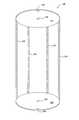
- FIG. 1is a schematic drawing of a wafer boat.
- FIG. 2is a schematic drawing of a support road with a notch.
- FIG. 3is a schematic drawing of a substrate resting within the notches of two support rods.
- FIG. 4is a schematic drawing of a wafer boat in relation to a deposition source.
- FIG. 5is a schematic drawing of a wafer boat in relation to a deposition source at another moment in time.
- the present inventiondescribes a method of uniformly depositing films within a batch processing chamber.
- a particularly good batch processing chamberthat can be used to practice the invention is described in U.S. patent application Ser. No. 11/249,555, filed Oct. 13, 2005, which is hereby incorporated by reference in its entirety.
- the inventionis illustratively described below with reference to a FLEXSTARTM system, available from Applied Materials, Inc., Santa Clara, Calif.
- FIG. 1is a schematic drawing of a substrate boat used in batch processing chambers. Other examples of substrate boats that can be used in batch processing are described in U.S. patent application Ser. No. 11/216,969, filed Aug. 31, 2005, which is hereby incorporated by reference in its entirety.
- FIG. 1shows a substrate boat 100 that can be used in the present invention.
- the substrate boat 100has a cap portion 101 and a base portion 102 .
- the cap portion 101 and the base portion 102are connected by several support rods 103 .
- the cap portion 101 and the base portion 102each have a slot 104 and a hole 105 .
- the slots 104are locations where the substrate boat 100 can be grasped for removal from the chamber, insertion into the chamber, and manipulation outside of the chamber.
- the holes 105are for connection to a rotation mechanism that will rotate the substrate boat 100 during processing.
- the substrate boat 100 shown in FIG. 1has four vertically extending support rods 103 . It should be understood that more or less support rods 103 can be present so long as sufficient support is provided for a substrate during processing.
- the support rods 103can be evenly spaced or they can be unevenly spaced around the circumference of the substrate boat 100 .
- FIG. 2shows a close up view of a notch 201 on a support rod 103 .
- the notch 201has a flat bottom surface 202 on which the substrate will rest, a vertical side surface 203 , and a slanted surface 204 .
- the notch 201need not be an opening within the support rod 103 .
- a ledge extending from the support rod 104could be used.
- the shape of the notch 201is not limited. So long as a notch or equivalent thereof can hold a substrate within the substrate boat without interfering with the deposition, it will be sufficient.
- FIG. 3shows a substrate 300 supported by two support rods 103 , each having a notch 201 .
- the substrate boat 100can be designed to hold any number of substrates.
- the substrate boat 100can be designed to hold 1 to 100 substrates 300 , with 51 substrates being preferred.
- ALDatomic layer deposition
- the precursorswill be provided to the substrate 300 from a deposition source located to the side of the substrate 300 .
- the deposition sourceis an injector assembly 400 that will provide the precursor gases through gas tubes 401 to outlet holes 402 within injection ports 403 .
- FIG. 4shows the injector assembly 400 together with a substrate boat 100 .
- the precursor gasis then dispersed within the chamber and, ideally, evenly over the substrates 300 . So long as nothing lies between the injection ports 403 and the substrates 300 , the precursor will be uniformly dispersed to the substrate 300 .
- the injector assembly 400has been shown with only five injection ports 403 , it should be understood that any number of injection ports 403 can be present. Ideally, the number of injection ports 403 will be equal to the maximum number of substrates 300 that can be held by the substrate boat 100 at one time. Additionally, it should be understood that the size of the injection ports 403 shown in the figures is not a representative size in relation to the substrate boat 100 . The injection ports 403 , gas tubes 401 , and holes 402 have been enlarged for ease of viewing.
- the support rods 103will inevitably block the line of sight path between the injection ports 403 and the substrates 300 .
- the precursorwill not be evenly distributed to the substrate 300 .
- the area of the substrate 300 that is blocked by the support rods 103will not receive an equal amount of precursor gas as the rest of the substrate 300 . Therefore, the precursor gas will not be uniformly provided to the substrate 300 .
- an uneven filmwill be deposited.
- FIG. 5shows the injector assembly 400 when it is behind one of the support rods 103 of the substrate boat 100 .
- the support rod 103is between the substrate 300 and the injector assembly 400 , portions of the substrate 300 that are behind the support rod 103 will not receive any of the precursor material.
- the areas of the substrate 300 that are not blocked by the support rod 103will be exposed to precursor material. Therefore, the precursor will not be evenly distributed to the substrate 300 .
- the precursoris delivered to the substrate in synchronized pulses in the following manner. As soon as the support rods 103 begin to get in between the substrate 300 and the injector assembly 400 , the precursor gas flow is shut off and the wafer boat 100 continues to rotate. Once the support rod 103 is clear of the injector assembly 400 , the precursor gas flow is restarted.
- Synchronizing the precursor gas flow pulses with the rotation of the substrate boat 100allows the precursor gas to always be uniformly provided to all areas of the substrate 300 .
- the synchronization of the precursor gas flow pulses in relation to the support rods 103can be set for rods that are evenly spaced around the substrate boat 100 . If the support rods are not evenly spaced around the substrate boat 100 , then the synchronization must take into account the location of the support rods 103 so that the precursor gas is timed to shut off whenever the support rods 103 block the line of sight path between the substrate 300 and the injector assembly 400 .
- the synchronizationcan be performed in numerous manners.
- One manner of synchronizationinvolves a specified timing schedule.
- the specified timing scheduleinvolves controlling the precursor to be provided to the substrate 300 at certain time intervals.
- the time intervalsare predetermined based upon a preset rotation rate of the substrate boat 100 .
- the substrate boat 100can be rotated at about 1 to about 30 rpm. Once the rotation rate is chosen and the support rod 103 spacing is known, the timing sequence of the precursor gas can be easily calculated.
- Another manner of synchronizing the precursor gas with the rotation of the substrate 300is to have a sensing mechanism that senses when the support rod 103 is beginning to block the line of sight path between the injector assembly 400 and the substrate.
- An additional sensorwould be provided to sense when the support rod 103 is no longer blocking the line of sight path between the substrate 300 and the injector assembly 400 .
- the sensorswould provide feedback to a central control unit that would control when and for how long the precursor gas is provided. Additional synchronization manners not mentioned herein could also be used without departing from the spirit of the invention.
- the ALD processwill typically be broken down into two separate cycles.
- the first precursorwill be provided to the substrate 300 .
- the first precursorwill be supplied to the substrate 300 for about 2 seconds to about 2 minutes. In another embodiment, the first precursor will be supplied to the substrate 300 for about 15 seconds or less.
- the chamberis evacuated to remove the first precursor gas. Following the evacuation, an inert purge gas is supplied to the chamber. Following the purge gas supply, the chamber will be evacuated. In one embodiment, the evacuation-purge-evacuation lasts about 2 seconds to about 5 minutes. In another embodiment, the evacuation-purge-evacuation lasts about 20 seconds.
- the second precursoris provided to the substrate 300 . In one embodiment, the second precursor will be supplied to the substrate 300 for about 2 seconds to about 2 minutes. In another embodiment, the second precursor is provided to the substrate 300 for about 15 seconds or less.
- filmscan be uniformly deposited on multiple substrates simultaneously.
- the synchronization of the substrate boat rotation and the timing of the depositionallow uninterrupted gas flow distribution to the substrate which results in improved film uniformity. Otherwise, uniformity degrades around the rod location.
- any conventional deposition methodsuch as physical vapor deposition, atomic layer deposition, and chemical vapor deposition may be performed by the current invention.
- any conventional substratecan be processed by the present invention including semiconductor substrates.
Landscapes
- Chemical & Material Sciences (AREA)
- General Chemical & Material Sciences (AREA)
- Chemical Kinetics & Catalysis (AREA)
- Engineering & Computer Science (AREA)
- Materials Engineering (AREA)
- Mechanical Engineering (AREA)
- Metallurgy (AREA)
- Organic Chemistry (AREA)
- Chemical Vapour Deposition (AREA)
Abstract
Description
- 1. Field of the Invention
- Embodiments of the present invention generally relate to deposition processes that are synchronized with wafer rotation.
- 2. Description of the Related Art
- The effectiveness of a substrate fabrication process is often measured by two related and important factors, device yield and cost of ownership. These factors are important because they directly affect the cost to produce an electronic device and therefore a device manufacturer's competitiveness within the marketplace. The cost of ownership, while affected by a number of factors, is greatly affected by the number of substrates processed per hour. Batch processing has become a popular method to reduce the cost of ownership. A batch processing chamber typically holds substrates in a substrate boat. Substrate boats can hold numerous substrates, but the support rods cause non-uniform deposition because they block the line of sight path between a deposition source and the substrate.
- There is a need in the art to reduce the cost of ownership in electronic device manufacturing while also providing a uniformly deposited film onto a substrate.
- The present invention generally provides a method of synchronizing the rotation of a substrate within a batch processing chamber in relation to the precursor gas flow into the chamber. By turning off the precursor gas flow into the chamber whenever a support rod of the substrate boat passes in front of the precursor gas injector panel, a uniform film can be deposited on a substrate.
- In a first embodiment, a method for depositing a layer on a substrate is disclosed. The method involves rotating a substrate holder within a chamber, providing a deposition material to the substrate as the substrate holder rotates, and stopping the provision of a deposition material to the substrate when a vertically extending rod is located between the source and the substrate. The substrate holder has at least one vertically extending rod located at a perimeter of the substrate. The vertically extending rod extends to a height greater than the substrate.
- In a second embodiment, an atomic layer deposition method is described. The method involves providing a substrate boat, rotating the substrate boat within a chamber, providing a first precursor from at least one injection port to the substrate while the substrate boat rotates, stopping the provision of the first precursor as each vertically extending rod rotates to a location between the injection port and the substrate, and providing the first precursor from the injector port to the substrate after the rod has rotated past the injection port. The substrate boat has a cap portion, a base portion, and a plurality of rods extending between the cap portion and the base portion. Each rod has at least one notch. An edge of a substrate can rest within one notch on each rod. The injection ports have an opening in a plane perpendicular to the substrate.
- In a third embodiment, a method of depositing a layer on a substrate is described. The method involves providing a substrate boat within a chamber, rotating the substrate boat, and depositing material onto the substrate as the substrate boat rotates. The material is provided from a deposition source. The substrate boat has a cap portion, a base portion, and a plurality of rods extending between the cap portion and the base portion. Each rod has at least one notch. An edge of the substrate can rest within one notch on each rod. The depositing is synchronized with the rotation such that during the time that the rod is located between the deposition source and the substrate, deposition material is not provided from the deposition source.
- So that the manner in which the above recited features of the present invention can be understood in detail, a more particular description of the invention, briefly summarized above, may be had by reference to embodiments, some of which are illustrated in the appended drawings. It is to be noted, however, that the appended drawings illustrate only typical embodiments of this invention and are therefore not to be considered limiting of its scope, for the invention may admit to other equally effective embodiments.
FIG. 1 is a schematic drawing of a wafer boat.FIG. 2 is a schematic drawing of a support road with a notch.FIG. 3 is a schematic drawing of a substrate resting within the notches of two support rods.FIG. 4 is a schematic drawing of a wafer boat in relation to a deposition source.FIG. 5 is a schematic drawing of a wafer boat in relation to a deposition source at another moment in time.- The present invention describes a method of uniformly depositing films within a batch processing chamber. A particularly good batch processing chamber that can be used to practice the invention is described in U.S. patent application Ser. No. 11/249,555, filed Oct. 13, 2005, which is hereby incorporated by reference in its entirety. The invention is illustratively described below with reference to a FLEXSTAR™ system, available from Applied Materials, Inc., Santa Clara, Calif.
FIG. 1 is a schematic drawing of a substrate boat used in batch processing chambers. Other examples of substrate boats that can be used in batch processing are described in U.S. patent application Ser. No. 11/216,969, filed Aug. 31, 2005, which is hereby incorporated by reference in its entirety.FIG. 1 shows asubstrate boat 100 that can be used in the present invention. Thesubstrate boat 100 has acap portion 101 and abase portion 102. Thecap portion 101 and thebase portion 102 are connected byseveral support rods 103. Thecap portion 101 and thebase portion 102 each have aslot 104 and ahole 105. Theslots 104 are locations where thesubstrate boat 100 can be grasped for removal from the chamber, insertion into the chamber, and manipulation outside of the chamber. Theholes 105 are for connection to a rotation mechanism that will rotate thesubstrate boat 100 during processing.- The
substrate boat 100 shown inFIG. 1 has four vertically extendingsupport rods 103. It should be understood that more orless support rods 103 can be present so long as sufficient support is provided for a substrate during processing. Thesupport rods 103 can be evenly spaced or they can be unevenly spaced around the circumference of thesubstrate boat 100. - Each
support rod 103 has a plurality ofnotches 201.FIG. 2 shows a close up view of anotch 201 on asupport rod 103. Thenotch 201 has aflat bottom surface 202 on which the substrate will rest, avertical side surface 203, and aslanted surface 204. It should be understood that thenotch 201 need not be an opening within thesupport rod 103. Instead of anotch 201, a ledge extending from thesupport rod 104 could be used. Additionally, the shape of thenotch 201 is not limited. So long as a notch or equivalent thereof can hold a substrate within the substrate boat without interfering with the deposition, it will be sufficient.FIG. 3 shows asubstrate 300 supported by twosupport rods 103, each having anotch 201. - The
substrate boat 100 can be designed to hold any number of substrates. Thesubstrate boat 100 can be designed to hold 1 to 100substrates 300, with 51 substrates being preferred. - To deposit a layer by atomic layer deposition (ALD) using the batch processing chamber, two separate precursors will be provided to the
substrate 300. A particularly good ALD process that can be practiced using the present invention is described in U.S. patent application Ser. No. 11/232,455, filed Sep. 21, 2005, which is hereby incorporated by reference in its entirety. The precursors will be provided to thesubstrate 300 from a deposition source located to the side of thesubstrate 300. The deposition source is aninjector assembly 400 that will provide the precursor gases throughgas tubes 401 to outlet holes402 withininjection ports 403.FIG. 4 shows theinjector assembly 400 together with asubstrate boat 100. The precursor gas is then dispersed within the chamber and, ideally, evenly over thesubstrates 300. So long as nothing lies between theinjection ports 403 and thesubstrates 300, the precursor will be uniformly dispersed to thesubstrate 300. - While the
injector assembly 400 has been shown with only fiveinjection ports 403, it should be understood that any number ofinjection ports 403 can be present. Ideally, the number ofinjection ports 403 will be equal to the maximum number ofsubstrates 300 that can be held by thesubstrate boat 100 at one time. Additionally, it should be understood that the size of theinjection ports 403 shown in the figures is not a representative size in relation to thesubstrate boat 100. Theinjection ports 403,gas tubes 401, and holes402 have been enlarged for ease of viewing. - As the
substrate boat 100 rotates, thesupport rods 103 will inevitably block the line of sight path between theinjection ports 403 and thesubstrates 300. When thesupport rods 103 are between thesubstrates 300 and theinjection ports 403, the precursor will not be evenly distributed to thesubstrate 300. The area of thesubstrate 300 that is blocked by thesupport rods 103 will not receive an equal amount of precursor gas as the rest of thesubstrate 300. Therefore, the precursor gas will not be uniformly provided to thesubstrate 300. When the precursor is not evenly provided to thesubstrate 300, an uneven film will be deposited. FIG. 5 shows theinjector assembly 400 when it is behind one of thesupport rods 103 of thesubstrate boat 100. When thesupport rod 103 is between thesubstrate 300 and theinjector assembly 400, portions of thesubstrate 300 that are behind thesupport rod 103 will not receive any of the precursor material. At the same time, the areas of thesubstrate 300 that are not blocked by thesupport rod 103 will be exposed to precursor material. Therefore, the precursor will not be evenly distributed to thesubstrate 300.- To prevent uneven distribution, the precursor is delivered to the substrate in synchronized pulses in the following manner. As soon as the
support rods 103 begin to get in between thesubstrate 300 and theinjector assembly 400, the precursor gas flow is shut off and thewafer boat 100 continues to rotate. Once thesupport rod 103 is clear of theinjector assembly 400, the precursor gas flow is restarted. - Synchronizing the precursor gas flow pulses with the rotation of the
substrate boat 100 allows the precursor gas to always be uniformly provided to all areas of thesubstrate 300. The synchronization of the precursor gas flow pulses in relation to thesupport rods 103 can be set for rods that are evenly spaced around thesubstrate boat 100. If the support rods are not evenly spaced around thesubstrate boat 100, then the synchronization must take into account the location of thesupport rods 103 so that the precursor gas is timed to shut off whenever thesupport rods 103 block the line of sight path between thesubstrate 300 and theinjector assembly 400. - The synchronization can be performed in numerous manners. One manner of synchronization involves a specified timing schedule. The specified timing schedule involves controlling the precursor to be provided to the
substrate 300 at certain time intervals. The time intervals are predetermined based upon a preset rotation rate of thesubstrate boat 100. Thesubstrate boat 100 can be rotated at about 1 to about 30 rpm. Once the rotation rate is chosen and thesupport rod 103 spacing is known, the timing sequence of the precursor gas can be easily calculated. - Another manner of synchronizing the precursor gas with the rotation of the
substrate 300 is to have a sensing mechanism that senses when thesupport rod 103 is beginning to block the line of sight path between theinjector assembly 400 and the substrate. An additional sensor would be provided to sense when thesupport rod 103 is no longer blocking the line of sight path between thesubstrate 300 and theinjector assembly 400. The sensors would provide feedback to a central control unit that would control when and for how long the precursor gas is provided. Additional synchronization manners not mentioned herein could also be used without departing from the spirit of the invention. - For a two component composite, the ALD process will typically be broken down into two separate cycles. In the first cycle, the first precursor will be provided to the
substrate 300. In one embodiment, the first precursor will be supplied to thesubstrate 300 for about 2 seconds to about 2 minutes. In another embodiment, the first precursor will be supplied to thesubstrate 300 for about 15 seconds or less. After the first precursor is provided to thesubstrate 300, the chamber is evacuated to remove the first precursor gas. Following the evacuation, an inert purge gas is supplied to the chamber. Following the purge gas supply, the chamber will be evacuated. In one embodiment, the evacuation-purge-evacuation lasts about 2 seconds to about 5 minutes. In another embodiment, the evacuation-purge-evacuation lasts about 20 seconds. Following the purge, the second precursor is provided to thesubstrate 300. In one embodiment, the second precursor will be supplied to thesubstrate 300 for about 2 seconds to about 2 minutes. In another embodiment, the second precursor is provided to thesubstrate 300 for about 15 seconds or less. - While a two component composite has been described above, it is to be understood that additional cycles can be present. The number of cycles will depend upon the number of precursors to be supplied. For example, in a three component system, a third precursor cycle will be necessary. All additional precursor cycles can be performed for the same time periods discussed above in relation to the first and second precursors. Additionally, the order that the precursors will be supplied depends upon the desired film to be formed. Between each precursor cycle, the evacuation-purge-evacuation described above will be performed. During the time period that the precursor gases are provided to the
substrate 300, it is to be understood that the synchronization of thesubstrate 300 rotation and the precursor gas flow as described above are occurring. - By synchronizing the rotation of the substrate boat with the timing of the deposition, films can be uniformly deposited on multiple substrates simultaneously. The synchronization of the substrate boat rotation and the timing of the deposition allow uninterrupted gas flow distribution to the substrate which results in improved film uniformity. Otherwise, uniformity degrades around the rod location.
- It is to be understood that any conventional deposition method such as physical vapor deposition, atomic layer deposition, and chemical vapor deposition may be performed by the current invention. Additionally, any conventional substrate can be processed by the present invention including semiconductor substrates.
- While the foregoing is directed to embodiments of the present invention, other and further embodiments of the invention may be devised without departing from the basic scope thereof, and the scope thereof is determined by the claims that follow.
Claims (20)
1. A method for depositing a layer on a substrate comprising:
rotating a substrate holder within a chamber, said substrate holder comprising at least one vertically extending rod located near an outer perimeter of said substrate, said vertically extending rod extending to a height greater than the substrate;
providing a deposition material to said substrate as said substrate rotates; and
stopping said providing of a deposition material to said substrate when said at least one vertically extending rod is located between said source and said substrate.
2. The method as claimed inclaim 1 , wherein the method for depositing is atomic layer deposition.
3. The method as claimed inclaim 1 , further comprising,
exhausting said chamber;
providing a second deposition material to said substrate as said substrate rotates; and
stopping said providing of a second deposition material to said substrate when said at least one vertically extending rod is located between said source and said substrate.
4. The method as claimed inclaim 1 , wherein said at least one vertically extending rod comprises a plurality of rods.
5. The method as claimed inclaim 4 , wherein said rods are evenly spaced around the perimeter of said substrate.
6. The method as claimed inclaim 4 , wherein said rods are not evenly spaced around the perimeter of said substrate.
7. The method as claimed inclaim 1 , further comprising providing said first deposition material after said at least one vertically extending rod has rotated past said source.
8. An atomic layer deposition method comprising:
providing a substrate boat, said substrate boat comprising:
a cap portion;
a base portion;
a plurality of rods extending between said cap portion and said base portion, each rod comprising at least one notch, wherein an edge of a substrate can rest within one notch on each rod;
rotating said substrate boat within a chamber;
providing a first precursor from at least one injection port to said substrate while said substrate boat rotates;
stopping said providing of the first precursor as the vertically extending rod rotates to a location between said injection port and said substrate;
providing said first precursor from said injector port to said substrate after each said rod has rotated past said injection port.
9. The method as claimed inclaim 8 , further comprising,
exhausting said chamber;
providing a second precursor from at least one injection port to said substrate while said substrate boat rotates; and
stopping said providing of the second precursor as each vertically extending rod rotates to a location between said injection port and said substrate.
10. The method as claimed inclaim 8 , wherein said notches on each rod are aligned with notches on all other rods such that said substrate is substantially level when placed within said substrate boat.
11. The method as claimed inclaim 8 , wherein said rods are evenly spaced around the perimeter of said substrate.
12. The method as claimed inclaim 8 , wherein said rods are not evenly spaced around the perimeter of said substrate.
13. The method as claimed inclaim 8 , wherein said at least one injection port comprises a plurality of injection ports.
14. A method of depositing a layer on a substrate comprising:
providing a substrate boat within a chamber, said substrate boat comprising:
a cap portion;
a base portion;
a plurality of rods extending between said cap portion and said base portion, each rod comprising at least one notch, wherein an edge of a substrate can rest within one notch on each rod;
rotating said substrate boat;
depositing material onto said substrate as said substrate boat rotates, said material provided from a deposition source, wherein said depositing is synchronized with said rotation such that during the time that said rod is located between said deposition source and said substrate, deposition material is not provided from said deposition source.
15. The method as claimed inclaim 14 , wherein said method of depositing comprises chemical vapor deposition, physical vapor deposition, or atomic layer deposition.
16. The method as claimed inclaim 14 , further comprising,
exhausting said chamber;
depositing a second material onto said substrate as said substrate boat rotates, said second material provided from a second deposition source, wherein said depositing is synchronized with said rotation such that during the time that each said rod is located between said second deposition source and said substrate, deposition material is not provided from said second deposition source.
17. The method as claimed inclaim 14 , wherein said notches on each rod are aligned with notches on all other rods such that said substrate is substantially level when placed within said substrate boat.
18. The method as claimed inclaim 14 , wherein said rods are evenly spaced around the perimeter of said substrate.
19. The method as claimed inclaim 14 , wherein said rods are not evenly spaced around the perimeter of said substrate.
20. The method as claimed inclaim 14 , wherein said deposition source comprises a plurality of injection ports.
Priority Applications (1)
| Application Number | Priority Date | Filing Date | Title |
|---|---|---|---|
| US11/413,658US20070252299A1 (en) | 2006-04-27 | 2006-04-27 | Synchronization of precursor pulsing and wafer rotation |
Applications Claiming Priority (1)
| Application Number | Priority Date | Filing Date | Title |
|---|---|---|---|
| US11/413,658US20070252299A1 (en) | 2006-04-27 | 2006-04-27 | Synchronization of precursor pulsing and wafer rotation |
Publications (1)
| Publication Number | Publication Date |
|---|---|
| US20070252299A1true US20070252299A1 (en) | 2007-11-01 |
Family
ID=38647594
Family Applications (1)
| Application Number | Title | Priority Date | Filing Date |
|---|---|---|---|
| US11/413,658AbandonedUS20070252299A1 (en) | 2006-04-27 | 2006-04-27 | Synchronization of precursor pulsing and wafer rotation |
Country Status (1)
| Country | Link |
|---|---|
| US (1) | US20070252299A1 (en) |
Cited By (3)
| Publication number | Priority date | Publication date | Assignee | Title |
|---|---|---|---|---|
| WO2014085307A3 (en)* | 2012-11-27 | 2014-07-24 | Intermolecular, Inc. | Combinatorial spin deposition |
| WO2016098183A1 (en)* | 2014-12-16 | 2016-06-23 | 株式会社日立国際電気 | Semiconductor device manufacturing method, substrate processing device, and recording medium |
| JP2019026939A (en)* | 2018-09-26 | 2019-02-21 | 株式会社Kokusai Electric | Semiconductor device manufacturing method, recording medium, and substrate processing apparatus |
Citations (92)
| Publication number | Priority date | Publication date | Assignee | Title |
|---|---|---|---|---|
| US4993357A (en)* | 1987-12-23 | 1991-02-19 | Cs Halbleiter -Und Solartechnologie Gmbh | Apparatus for atomic layer epitaxial growth |
| US5178681A (en)* | 1991-01-29 | 1993-01-12 | Applied Materials, Inc. | Suspension system for semiconductor reactors |
| US5281274A (en)* | 1990-06-22 | 1994-01-25 | The United States Of America As Represented By The Secretary Of The Navy | Atomic layer epitaxy (ALE) apparatus for growing thin films of elemental semiconductors |
| US5480818A (en)* | 1992-02-10 | 1996-01-02 | Fujitsu Limited | Method for forming a film and method for manufacturing a thin film transistor |
| US5483919A (en)* | 1990-08-31 | 1996-01-16 | Nippon Telegraph And Telephone Corporation | Atomic layer epitaxy method and apparatus |
| US5711811A (en)* | 1994-11-28 | 1998-01-27 | Mikrokemia Oy | Method and equipment for growing thin films |
| US5855680A (en)* | 1994-11-28 | 1999-01-05 | Neste Oy | Apparatus for growing thin films |
| US6013553A (en)* | 1997-07-24 | 2000-01-11 | Texas Instruments Incorporated | Zirconium and/or hafnium oxynitride gate dielectric |
| US6015917A (en)* | 1998-01-23 | 2000-01-18 | Advanced Technology Materials, Inc. | Tantalum amide precursors for deposition of tantalum nitride on a substrate |
| US6015590A (en)* | 1994-11-28 | 2000-01-18 | Neste Oy | Method for growing thin films |
| US6174809B1 (en)* | 1997-12-31 | 2001-01-16 | Samsung Electronics, Co., Ltd. | Method for forming metal layer using atomic layer deposition |
| US6174377B1 (en)* | 1997-03-03 | 2001-01-16 | Genus, Inc. | Processing chamber for atomic layer deposition processes |
| US6183563B1 (en)* | 1998-05-18 | 2001-02-06 | Ips Ltd. | Apparatus for depositing thin films on semiconductor wafers |
| US6335240B1 (en)* | 1998-01-06 | 2002-01-01 | Samsung Electronics Co., Ltd. | Capacitor for a semiconductor device and method for forming the same |
| US20020000598A1 (en)* | 1999-12-08 | 2002-01-03 | Sang-Bom Kang | Semiconductor devices having metal layers as barrier layers on upper or lower electrodes of capacitors |
| US20020000196A1 (en)* | 2000-06-24 | 2002-01-03 | Park Young-Hoon | Reactor for depositing thin film on wafer |
| US20020005168A1 (en)* | 1999-11-30 | 2002-01-17 | Applied Materials, Inc. | Dual wafer load lock |
| US20020005556A1 (en)* | 1999-10-06 | 2002-01-17 | Eduard Albert Cartier | Silicate gate dielectric |
| US20020007790A1 (en)* | 2000-07-22 | 2002-01-24 | Park Young-Hoon | Atomic layer deposition (ALD) thin film deposition equipment having cleaning apparatus and cleaning method |
| US20020009896A1 (en)* | 1996-05-31 | 2002-01-24 | Sandhu Gurtej S. | Chemical vapor deposition using organometallic precursors |
| US20020008297A1 (en)* | 2000-06-28 | 2002-01-24 | Dae-Gyu Park | Gate structure and method for manufacture thereof |
| US20020009544A1 (en)* | 1999-08-20 | 2002-01-24 | Mcfeely F. Read | Delivery systems for gases for gases via the sublimation of solid precursors |
| US6342277B1 (en)* | 1996-08-16 | 2002-01-29 | Licensee For Microelectronics: Asm America, Inc. | Sequential chemical vapor deposition |
| US20020015790A1 (en)* | 1999-10-07 | 2002-02-07 | Advanced Technology Materials Inc. | Source reagent compositions for CVD formation of high dielectric constant and ferroelectric metal oxide thin films and method of using same |
| US20020016084A1 (en)* | 2000-04-28 | 2002-02-07 | Todd Michael A. | CVD syntheses of silicon nitride materials |
| US20020014647A1 (en)* | 2000-07-07 | 2002-02-07 | Infineon Technologies Ag | Trench capacitor with isolation collar and corresponding method of production |
| US20020017242A1 (en)* | 2000-05-25 | 2002-02-14 | Kabushiki Kaisha Kobe Seiko Sho (Kobe Steel, Ltd.) | Inner tube for CVD apparatus |
| US6348386B1 (en)* | 2001-04-16 | 2002-02-19 | Motorola, Inc. | Method for making a hafnium-based insulating film |
| US6348376B2 (en)* | 1997-09-29 | 2002-02-19 | Samsung Electronics Co., Ltd. | Method of forming metal nitride film by chemical vapor deposition and method of forming metal contact and capacitor of semiconductor device using the same |
| US20020021544A1 (en)* | 2000-08-11 | 2002-02-21 | Hag-Ju Cho | Integrated circuit devices having dielectric regions protected with multi-layer insulation structures and methods of fabricating same |
| US20020020869A1 (en)* | 1999-12-22 | 2002-02-21 | Ki-Seon Park | Semiconductor device incorporated therein high K capacitor dielectric and method for the manufacture thereof |
| US20030004723A1 (en)* | 2001-06-26 | 2003-01-02 | Keiichi Chihara | Method of controlling high-speed reading in a text-to-speech conversion system |
| US20030013300A1 (en)* | 2001-07-16 | 2003-01-16 | Applied Materials, Inc. | Method and apparatus for depositing tungsten after surface treatment to improve film characteristics |
| US20030010451A1 (en)* | 2001-07-16 | 2003-01-16 | Applied Materials, Inc. | Lid assembly for a processing system to facilitate sequential deposition techniques |
| US20030013320A1 (en)* | 2001-05-31 | 2003-01-16 | Samsung Electronics Co., Ltd. | Method of forming a thin film using atomic layer deposition |
| US20030017697A1 (en)* | 2001-07-19 | 2003-01-23 | Kyung-In Choi | Methods of forming metal layers using metallic precursors |
| US20030015764A1 (en)* | 2001-06-21 | 2003-01-23 | Ivo Raaijmakers | Trench isolation for integrated circuit |
| US6511539B1 (en)* | 1999-09-08 | 2003-01-28 | Asm America, Inc. | Apparatus and method for growth of a thin film |
| US20030022338A1 (en)* | 1999-11-22 | 2003-01-30 | Human Genome Sciences, Inc. | Kunitz-type protease inhibitor polynucleotides, polypeptides, and antibodies |
| US20030022487A1 (en)* | 2001-07-25 | 2003-01-30 | Applied Materials, Inc. | Barrier formation using novel sputter-deposition method |
| US20030022507A1 (en)* | 2001-05-07 | 2003-01-30 | Applied Materials, Inc. | CVD TiSiN barrier for copper integration |
| US20030033281A1 (en)* | 2000-04-24 | 2003-02-13 | Ritz Charles D. | Method and apparatus for increasing the capacity and stability of a single-pole tower |
| US20030031807A1 (en)* | 1999-10-15 | 2003-02-13 | Kai-Erik Elers | Deposition of transition metal carbides |
| US6524952B1 (en)* | 1999-06-25 | 2003-02-25 | Applied Materials, Inc. | Method of forming a titanium silicide layer on a substrate |
| US20030038369A1 (en)* | 2001-08-22 | 2003-02-27 | Nace Layadi | Method for reducing a metal seam in an interconnect structure and a device manufactured thereby |
| US6674138B1 (en)* | 2001-12-31 | 2004-01-06 | Advanced Micro Devices, Inc. | Use of high-k dielectric materials in modified ONO structure for semiconductor devices |
| US20040005749A1 (en)* | 2002-07-02 | 2004-01-08 | Choi Gil-Heyun | Methods of forming dual gate semiconductor devices having a metal nitride layer |
| US6677247B2 (en)* | 2002-01-07 | 2004-01-13 | Applied Materials Inc. | Method of increasing the etch selectivity of a contact sidewall to a preclean etchant |
| US20040009336A1 (en)* | 2002-07-11 | 2004-01-15 | Applied Materials, Inc. | Titanium silicon nitride (TISIN) barrier layer for copper diffusion |
| US20040009675A1 (en)* | 2002-07-15 | 2004-01-15 | Eissa Mona M. | Gate structure and method |
| US20040009307A1 (en)* | 2000-06-08 | 2004-01-15 | Won-Yong Koh | Thin film forming method |
| US20040007747A1 (en)* | 2002-07-15 | 2004-01-15 | Visokay Mark R. | Gate structure and method |
| US20040011504A1 (en)* | 2002-07-17 | 2004-01-22 | Ku Vincent W. | Method and apparatus for gas temperature control in a semiconductor processing system |
| US20040013577A1 (en)* | 2002-07-17 | 2004-01-22 | Seshadri Ganguli | Method and apparatus for providing gas to a processing chamber |
| US20040015300A1 (en)* | 2002-07-22 | 2004-01-22 | Seshadri Ganguli | Method and apparatus for monitoring solid precursor delivery |
| US20040011404A1 (en)* | 2002-07-19 | 2004-01-22 | Ku Vincent W | Valve design and configuration for fast delivery system |
| US20040013803A1 (en)* | 2002-07-16 | 2004-01-22 | Applied Materials, Inc. | Formation of titanium nitride films using a cyclical deposition process |
| US20040016404A1 (en)* | 2002-07-23 | 2004-01-29 | John Gregg | Vaporizer delivery ampoule |
| US20040016973A1 (en)* | 2002-07-26 | 2004-01-29 | Rotondaro Antonio L.P. | Gate dielectric and method |
| US20040018304A1 (en)* | 2002-07-10 | 2004-01-29 | Applied Materials, Inc. | Method of film deposition using activated precursor gases |
| US20040018723A1 (en)* | 2000-06-27 | 2004-01-29 | Applied Materials, Inc. | Formation of boride barrier layers using chemisorption techniques |
| US20040018747A1 (en)* | 2002-07-20 | 2004-01-29 | Lee Jung-Hyun | Deposition method of a dielectric layer |
| US20040018738A1 (en)* | 2002-07-22 | 2004-01-29 | Wei Liu | Method for fabricating a notch gate structure of a field effect transistor |
| US6686271B2 (en)* | 2000-05-15 | 2004-02-03 | Asm International N.V. | Protective layers prior to alternating layer deposition |
| US20040023462A1 (en)* | 2002-07-31 | 2004-02-05 | Rotondaro Antonio L.P. | Gate dielectric and method |
| US20040023461A1 (en)* | 2002-07-30 | 2004-02-05 | Micron Technology, Inc. | Atomic layer deposited nanolaminates of HfO2/ZrO2 films as gate dielectrics |
| US20040024506A1 (en)* | 2002-08-01 | 2004-02-05 | Augustine Michael J. | Vehicle steering system with visual feedback display |
| US20040029321A1 (en)* | 2002-08-07 | 2004-02-12 | Chartered Semiconductor Manufacturing Ltd. | Method for forming gate insulating layer having multiple dielectric constants and multiple equivalent oxide thicknesses |
| US20040028952A1 (en)* | 2002-06-10 | 2004-02-12 | Interuniversitair Microelektronica Centrum (Imec Vzw) | High dielectric constant composition and method of making same |
| US20040025370A1 (en)* | 2002-07-29 | 2004-02-12 | Applied Materials, Inc. | Method and apparatus for generating gas to a processing chamber |
| US20040033698A1 (en)* | 2002-08-17 | 2004-02-19 | Lee Yun-Jung | Method of forming oxide layer using atomic layer deposition method and method of forming capacitor of semiconductor device using the same |
| US20040038486A1 (en)* | 2002-06-12 | 2004-02-26 | Applied Materials, Inc. | Plasma method and apparatus for processing a substrate |
| US20040038554A1 (en)* | 2002-08-21 | 2004-02-26 | Ahn Kie Y. | Composite dielectric forming methods and composite dielectrics |
| US20040036111A1 (en)* | 2002-03-26 | 2004-02-26 | Matsushita Electric Industrial Co., Ltd. | Semiconductor device and a fabrication method thereof |
| US20050009325A1 (en)* | 2003-06-18 | 2005-01-13 | Hua Chung | Atomic layer deposition of barrier materials |
| US20050006799A1 (en)* | 2002-07-23 | 2005-01-13 | Gregg John N. | Method and apparatus to help promote contact of gas with vaporized material |
| US20050009371A1 (en)* | 2002-06-14 | 2005-01-13 | Metzner Craig R. | System and method for forming a gate dielectric |
| US20050008779A1 (en)* | 2002-04-08 | 2005-01-13 | Yang Michael Xi | Multiple precursor cyclical depositon system |
| US20050012975A1 (en)* | 2002-12-17 | 2005-01-20 | George Steven M. | Al2O3 atomic layer deposition to enhance the deposition of hydrophobic or hydrophilic coatings on micro-electromechcanical devices |
| US6849545B2 (en)* | 2001-06-20 | 2005-02-01 | Applied Materials, Inc. | System and method to form a composite film stack utilizing sequential deposition techniques |
| US20050037627A1 (en)* | 2001-11-30 | 2005-02-17 | Christian Dussarrat | Method for depositing silicon nitride films and silicon oxynitride films by chemical vapor deposition |
| US6983892B2 (en)* | 2004-02-05 | 2006-01-10 | Applied Materials, Inc. | Gas distribution showerhead for semiconductor processing |
| US20060019032A1 (en)* | 2004-07-23 | 2006-01-26 | Yaxin Wang | Low thermal budget silicon nitride formation for advance transistor fabrication |
| US20060019033A1 (en)* | 2004-05-21 | 2006-01-26 | Applied Materials, Inc. | Plasma treatment of hafnium-containing materials |
| US20060019495A1 (en)* | 2004-07-20 | 2006-01-26 | Applied Materials, Inc. | Atomic layer deposition of tantalum-containing materials using the tantalum precursor taimata |
| US20060019494A1 (en)* | 2002-03-04 | 2006-01-26 | Wei Cao | Sequential deposition of tantalum nitride using a tantalum-containing precursor and a nitrogen-containing precursor |
| US20060018639A1 (en)* | 2003-10-27 | 2006-01-26 | Sundar Ramamurthy | Processing multilayer semiconductors with multiple heat sources |
| US20060030148A1 (en)* | 2001-02-02 | 2006-02-09 | Applied Materials, Inc. | Formation of a tantalum-nitride layer |
| US20060035025A1 (en)* | 2002-10-11 | 2006-02-16 | Applied Materials, Inc. | Activated species generator for rapid cycle deposition processes |
| US20070003698A1 (en)* | 2001-10-26 | 2007-01-04 | Ling Chen | Enhanced copper growth with ultrathin barrier layer for high performance interconnects |
| US20070020890A1 (en)* | 2005-07-19 | 2007-01-25 | Applied Materials, Inc. | Method and apparatus for semiconductor processing |
| US20070018244A1 (en)* | 2005-07-20 | 2007-01-25 | Applied Materials, Inc. | Gate Electrode structures and methods of manufacture |
- 2006
- 2006-04-27USUS11/413,658patent/US20070252299A1/ennot_activeAbandoned
Patent Citations (99)
| Publication number | Priority date | Publication date | Assignee | Title |
|---|---|---|---|---|
| US4993357A (en)* | 1987-12-23 | 1991-02-19 | Cs Halbleiter -Und Solartechnologie Gmbh | Apparatus for atomic layer epitaxial growth |
| US5281274A (en)* | 1990-06-22 | 1994-01-25 | The United States Of America As Represented By The Secretary Of The Navy | Atomic layer epitaxy (ALE) apparatus for growing thin films of elemental semiconductors |
| US5483919A (en)* | 1990-08-31 | 1996-01-16 | Nippon Telegraph And Telephone Corporation | Atomic layer epitaxy method and apparatus |
| US5178681A (en)* | 1991-01-29 | 1993-01-12 | Applied Materials, Inc. | Suspension system for semiconductor reactors |
| US5480818A (en)* | 1992-02-10 | 1996-01-02 | Fujitsu Limited | Method for forming a film and method for manufacturing a thin film transistor |
| US5855680A (en)* | 1994-11-28 | 1999-01-05 | Neste Oy | Apparatus for growing thin films |
| US5711811A (en)* | 1994-11-28 | 1998-01-27 | Mikrokemia Oy | Method and equipment for growing thin films |
| US6015590A (en)* | 1994-11-28 | 2000-01-18 | Neste Oy | Method for growing thin films |
| US20020009896A1 (en)* | 1996-05-31 | 2002-01-24 | Sandhu Gurtej S. | Chemical vapor deposition using organometallic precursors |
| US6342277B1 (en)* | 1996-08-16 | 2002-01-29 | Licensee For Microelectronics: Asm America, Inc. | Sequential chemical vapor deposition |
| US6174377B1 (en)* | 1997-03-03 | 2001-01-16 | Genus, Inc. | Processing chamber for atomic layer deposition processes |
| US6013553A (en)* | 1997-07-24 | 2000-01-11 | Texas Instruments Incorporated | Zirconium and/or hafnium oxynitride gate dielectric |
| US6020243A (en)* | 1997-07-24 | 2000-02-01 | Texas Instruments Incorporated | Zirconium and/or hafnium silicon-oxynitride gate dielectric |
| US6348376B2 (en)* | 1997-09-29 | 2002-02-19 | Samsung Electronics Co., Ltd. | Method of forming metal nitride film by chemical vapor deposition and method of forming metal contact and capacitor of semiconductor device using the same |
| US6174809B1 (en)* | 1997-12-31 | 2001-01-16 | Samsung Electronics, Co., Ltd. | Method for forming metal layer using atomic layer deposition |
| US6335240B1 (en)* | 1998-01-06 | 2002-01-01 | Samsung Electronics Co., Ltd. | Capacitor for a semiconductor device and method for forming the same |
| US6015917A (en)* | 1998-01-23 | 2000-01-18 | Advanced Technology Materials, Inc. | Tantalum amide precursors for deposition of tantalum nitride on a substrate |
| US6183563B1 (en)* | 1998-05-18 | 2001-02-06 | Ips Ltd. | Apparatus for depositing thin films on semiconductor wafers |
| US6524952B1 (en)* | 1999-06-25 | 2003-02-25 | Applied Materials, Inc. | Method of forming a titanium silicide layer on a substrate |
| US20020009544A1 (en)* | 1999-08-20 | 2002-01-24 | Mcfeely F. Read | Delivery systems for gases for gases via the sublimation of solid precursors |
| US6511539B1 (en)* | 1999-09-08 | 2003-01-28 | Asm America, Inc. | Apparatus and method for growth of a thin film |
| US20020005556A1 (en)* | 1999-10-06 | 2002-01-17 | Eduard Albert Cartier | Silicate gate dielectric |
| US20020015790A1 (en)* | 1999-10-07 | 2002-02-07 | Advanced Technology Materials Inc. | Source reagent compositions for CVD formation of high dielectric constant and ferroelectric metal oxide thin films and method of using same |
| US20030031807A1 (en)* | 1999-10-15 | 2003-02-13 | Kai-Erik Elers | Deposition of transition metal carbides |
| US20030022338A1 (en)* | 1999-11-22 | 2003-01-30 | Human Genome Sciences, Inc. | Kunitz-type protease inhibitor polynucleotides, polypeptides, and antibodies |
| US6841200B2 (en)* | 1999-11-30 | 2005-01-11 | Applied Materials, Inc. | Dual wafer load lock |
| US20020005168A1 (en)* | 1999-11-30 | 2002-01-17 | Applied Materials, Inc. | Dual wafer load lock |
| US20020000598A1 (en)* | 1999-12-08 | 2002-01-03 | Sang-Bom Kang | Semiconductor devices having metal layers as barrier layers on upper or lower electrodes of capacitors |
| US20020020869A1 (en)* | 1999-12-22 | 2002-02-21 | Ki-Seon Park | Semiconductor device incorporated therein high K capacitor dielectric and method for the manufacture thereof |
| US20030033281A1 (en)* | 2000-04-24 | 2003-02-13 | Ritz Charles D. | Method and apparatus for increasing the capacity and stability of a single-pole tower |
| US20020016084A1 (en)* | 2000-04-28 | 2002-02-07 | Todd Michael A. | CVD syntheses of silicon nitride materials |
| US6686271B2 (en)* | 2000-05-15 | 2004-02-03 | Asm International N.V. | Protective layers prior to alternating layer deposition |
| US20020017242A1 (en)* | 2000-05-25 | 2002-02-14 | Kabushiki Kaisha Kobe Seiko Sho (Kobe Steel, Ltd.) | Inner tube for CVD apparatus |
| US20040009307A1 (en)* | 2000-06-08 | 2004-01-15 | Won-Yong Koh | Thin film forming method |
| US20020000196A1 (en)* | 2000-06-24 | 2002-01-03 | Park Young-Hoon | Reactor for depositing thin film on wafer |
| US20040018723A1 (en)* | 2000-06-27 | 2004-01-29 | Applied Materials, Inc. | Formation of boride barrier layers using chemisorption techniques |
| US20020008297A1 (en)* | 2000-06-28 | 2002-01-24 | Dae-Gyu Park | Gate structure and method for manufacture thereof |
| US20020014647A1 (en)* | 2000-07-07 | 2002-02-07 | Infineon Technologies Ag | Trench capacitor with isolation collar and corresponding method of production |
| US20020007790A1 (en)* | 2000-07-22 | 2002-01-24 | Park Young-Hoon | Atomic layer deposition (ALD) thin film deposition equipment having cleaning apparatus and cleaning method |
| US20020021544A1 (en)* | 2000-08-11 | 2002-02-21 | Hag-Ju Cho | Integrated circuit devices having dielectric regions protected with multi-layer insulation structures and methods of fabricating same |
| US20060030148A1 (en)* | 2001-02-02 | 2006-02-09 | Applied Materials, Inc. | Formation of a tantalum-nitride layer |
| US6348386B1 (en)* | 2001-04-16 | 2002-02-19 | Motorola, Inc. | Method for making a hafnium-based insulating film |
| US20030022507A1 (en)* | 2001-05-07 | 2003-01-30 | Applied Materials, Inc. | CVD TiSiN barrier for copper integration |
| US20030013320A1 (en)* | 2001-05-31 | 2003-01-16 | Samsung Electronics Co., Ltd. | Method of forming a thin film using atomic layer deposition |
| US6849545B2 (en)* | 2001-06-20 | 2005-02-01 | Applied Materials, Inc. | System and method to form a composite film stack utilizing sequential deposition techniques |
| US20030015764A1 (en)* | 2001-06-21 | 2003-01-23 | Ivo Raaijmakers | Trench isolation for integrated circuit |
| US20030004723A1 (en)* | 2001-06-26 | 2003-01-02 | Keiichi Chihara | Method of controlling high-speed reading in a text-to-speech conversion system |
| US20030010451A1 (en)* | 2001-07-16 | 2003-01-16 | Applied Materials, Inc. | Lid assembly for a processing system to facilitate sequential deposition techniques |
| US20030013300A1 (en)* | 2001-07-16 | 2003-01-16 | Applied Materials, Inc. | Method and apparatus for depositing tungsten after surface treatment to improve film characteristics |
| US20030017697A1 (en)* | 2001-07-19 | 2003-01-23 | Kyung-In Choi | Methods of forming metal layers using metallic precursors |
| US20030029715A1 (en)* | 2001-07-25 | 2003-02-13 | Applied Materials, Inc. | An Apparatus For Annealing Substrates In Physical Vapor Deposition Systems |
| US20030022487A1 (en)* | 2001-07-25 | 2003-01-30 | Applied Materials, Inc. | Barrier formation using novel sputter-deposition method |
| US20030038369A1 (en)* | 2001-08-22 | 2003-02-27 | Nace Layadi | Method for reducing a metal seam in an interconnect structure and a device manufactured thereby |
| US20070003698A1 (en)* | 2001-10-26 | 2007-01-04 | Ling Chen | Enhanced copper growth with ultrathin barrier layer for high performance interconnects |
| US20050037627A1 (en)* | 2001-11-30 | 2005-02-17 | Christian Dussarrat | Method for depositing silicon nitride films and silicon oxynitride films by chemical vapor deposition |
| US6674138B1 (en)* | 2001-12-31 | 2004-01-06 | Advanced Micro Devices, Inc. | Use of high-k dielectric materials in modified ONO structure for semiconductor devices |
| US6677247B2 (en)* | 2002-01-07 | 2004-01-13 | Applied Materials Inc. | Method of increasing the etch selectivity of a contact sidewall to a preclean etchant |
| US20060019494A1 (en)* | 2002-03-04 | 2006-01-26 | Wei Cao | Sequential deposition of tantalum nitride using a tantalum-containing precursor and a nitrogen-containing precursor |
| US20040036111A1 (en)* | 2002-03-26 | 2004-02-26 | Matsushita Electric Industrial Co., Ltd. | Semiconductor device and a fabrication method thereof |
| US6846516B2 (en)* | 2002-04-08 | 2005-01-25 | Applied Materials, Inc. | Multiple precursor cyclical deposition system |
| US20050008779A1 (en)* | 2002-04-08 | 2005-01-13 | Yang Michael Xi | Multiple precursor cyclical depositon system |
| US20040028952A1 (en)* | 2002-06-10 | 2004-02-12 | Interuniversitair Microelektronica Centrum (Imec Vzw) | High dielectric constant composition and method of making same |
| US20040038486A1 (en)* | 2002-06-12 | 2004-02-26 | Applied Materials, Inc. | Plasma method and apparatus for processing a substrate |
| US6858547B2 (en)* | 2002-06-14 | 2005-02-22 | Applied Materials, Inc. | System and method for forming a gate dielectric |
| US20050009371A1 (en)* | 2002-06-14 | 2005-01-13 | Metzner Craig R. | System and method for forming a gate dielectric |
| US20040005749A1 (en)* | 2002-07-02 | 2004-01-08 | Choi Gil-Heyun | Methods of forming dual gate semiconductor devices having a metal nitride layer |
| US6838125B2 (en)* | 2002-07-10 | 2005-01-04 | Applied Materials, Inc. | Method of film deposition using activated precursor gases |
| US20040018304A1 (en)* | 2002-07-10 | 2004-01-29 | Applied Materials, Inc. | Method of film deposition using activated precursor gases |
| US20040009336A1 (en)* | 2002-07-11 | 2004-01-15 | Applied Materials, Inc. | Titanium silicon nitride (TISIN) barrier layer for copper diffusion |
| US20040009675A1 (en)* | 2002-07-15 | 2004-01-15 | Eissa Mona M. | Gate structure and method |
| US20040007747A1 (en)* | 2002-07-15 | 2004-01-15 | Visokay Mark R. | Gate structure and method |
| US20040013803A1 (en)* | 2002-07-16 | 2004-01-22 | Applied Materials, Inc. | Formation of titanium nitride films using a cyclical deposition process |
| US20040014320A1 (en)* | 2002-07-17 | 2004-01-22 | Applied Materials, Inc. | Method and apparatus of generating PDMAT precursor |
| US20040013577A1 (en)* | 2002-07-17 | 2004-01-22 | Seshadri Ganguli | Method and apparatus for providing gas to a processing chamber |
| US20040011504A1 (en)* | 2002-07-17 | 2004-01-22 | Ku Vincent W. | Method and apparatus for gas temperature control in a semiconductor processing system |
| US20040011404A1 (en)* | 2002-07-19 | 2004-01-22 | Ku Vincent W | Valve design and configuration for fast delivery system |
| US20040018747A1 (en)* | 2002-07-20 | 2004-01-29 | Lee Jung-Hyun | Deposition method of a dielectric layer |
| US20040018738A1 (en)* | 2002-07-22 | 2004-01-29 | Wei Liu | Method for fabricating a notch gate structure of a field effect transistor |
| US20040015300A1 (en)* | 2002-07-22 | 2004-01-22 | Seshadri Ganguli | Method and apparatus for monitoring solid precursor delivery |
| US20040016404A1 (en)* | 2002-07-23 | 2004-01-29 | John Gregg | Vaporizer delivery ampoule |
| US20050006799A1 (en)* | 2002-07-23 | 2005-01-13 | Gregg John N. | Method and apparatus to help promote contact of gas with vaporized material |
| US20040016973A1 (en)* | 2002-07-26 | 2004-01-29 | Rotondaro Antonio L.P. | Gate dielectric and method |
| US20040025370A1 (en)* | 2002-07-29 | 2004-02-12 | Applied Materials, Inc. | Method and apparatus for generating gas to a processing chamber |
| US20040023461A1 (en)* | 2002-07-30 | 2004-02-05 | Micron Technology, Inc. | Atomic layer deposited nanolaminates of HfO2/ZrO2 films as gate dielectrics |
| US20040023462A1 (en)* | 2002-07-31 | 2004-02-05 | Rotondaro Antonio L.P. | Gate dielectric and method |
| US20040024506A1 (en)* | 2002-08-01 | 2004-02-05 | Augustine Michael J. | Vehicle steering system with visual feedback display |
| US20040029321A1 (en)* | 2002-08-07 | 2004-02-12 | Chartered Semiconductor Manufacturing Ltd. | Method for forming gate insulating layer having multiple dielectric constants and multiple equivalent oxide thicknesses |
| US20040033698A1 (en)* | 2002-08-17 | 2004-02-19 | Lee Yun-Jung | Method of forming oxide layer using atomic layer deposition method and method of forming capacitor of semiconductor device using the same |
| US20040038554A1 (en)* | 2002-08-21 | 2004-02-26 | Ahn Kie Y. | Composite dielectric forming methods and composite dielectrics |
| US20060035025A1 (en)* | 2002-10-11 | 2006-02-16 | Applied Materials, Inc. | Activated species generator for rapid cycle deposition processes |
| US20050012975A1 (en)* | 2002-12-17 | 2005-01-20 | George Steven M. | Al2O3 atomic layer deposition to enhance the deposition of hydrophobic or hydrophilic coatings on micro-electromechcanical devices |
| US20050009325A1 (en)* | 2003-06-18 | 2005-01-13 | Hua Chung | Atomic layer deposition of barrier materials |
| US20060018639A1 (en)* | 2003-10-27 | 2006-01-26 | Sundar Ramamurthy | Processing multilayer semiconductors with multiple heat sources |
| US6983892B2 (en)* | 2004-02-05 | 2006-01-10 | Applied Materials, Inc. | Gas distribution showerhead for semiconductor processing |
| US20060019033A1 (en)* | 2004-05-21 | 2006-01-26 | Applied Materials, Inc. | Plasma treatment of hafnium-containing materials |
| US20060019495A1 (en)* | 2004-07-20 | 2006-01-26 | Applied Materials, Inc. | Atomic layer deposition of tantalum-containing materials using the tantalum precursor taimata |
| US20060019032A1 (en)* | 2004-07-23 | 2006-01-26 | Yaxin Wang | Low thermal budget silicon nitride formation for advance transistor fabrication |
| US20070020890A1 (en)* | 2005-07-19 | 2007-01-25 | Applied Materials, Inc. | Method and apparatus for semiconductor processing |
| US20070018244A1 (en)* | 2005-07-20 | 2007-01-25 | Applied Materials, Inc. | Gate Electrode structures and methods of manufacture |
Cited By (6)
| Publication number | Priority date | Publication date | Assignee | Title |
|---|---|---|---|---|
| WO2014085307A3 (en)* | 2012-11-27 | 2014-07-24 | Intermolecular, Inc. | Combinatorial spin deposition |
| WO2016098183A1 (en)* | 2014-12-16 | 2016-06-23 | 株式会社日立国際電気 | Semiconductor device manufacturing method, substrate processing device, and recording medium |
| JPWO2016098183A1 (en)* | 2014-12-16 | 2017-08-10 | 株式会社日立国際電気 | Semiconductor device manufacturing method, substrate processing apparatus, and recording medium |
| US20170287716A1 (en)* | 2014-12-16 | 2017-10-05 | Hitachi Kokusai Electric Inc. | Method of manufacturing semiconductor device |
| US10622213B2 (en)* | 2014-12-16 | 2020-04-14 | Kokusai Electric Corporation | Method of manufacturing semiconductor device |
| JP2019026939A (en)* | 2018-09-26 | 2019-02-21 | 株式会社Kokusai Electric | Semiconductor device manufacturing method, recording medium, and substrate processing apparatus |
Similar Documents
| Publication | Publication Date | Title |
|---|---|---|
| JP5177591B2 (en) | Batch type atomic layer deposition equipment | |
| JP5722516B2 (en) | Atomic layer CVD | |
| US6040011A (en) | Substrate support member with a purge gas channel and pumping system | |
| US8691708B2 (en) | Method of manufacturing semiconductor device and substrate processing apparatus | |
| JP5619164B2 (en) | CVD method and CVD reactor | |
| US9929008B2 (en) | Substrate processing method and substrate processing apparatus | |
| JP7464692B2 (en) | Evaporator chamber for forming a film on a substrate | |
| KR20070088184A (en) | Shower head and atomic layer deposition equipment | |
| US20070252299A1 (en) | Synchronization of precursor pulsing and wafer rotation | |
| EP2310552A2 (en) | Gas delivery device | |
| KR101573689B1 (en) | The apparatus for depositing the atomic layer | |
| KR100733573B1 (en) | Chemical vapor deposition system using showerhead | |
| US20200219745A1 (en) | Substrate processing apparatus and recording medium | |
| KR100422398B1 (en) | Apparatus for depositing a thin film | |
| US11721566B2 (en) | Sensor assembly and methods of vapor monitoring in process chambers | |
| KR102497746B1 (en) | Subtrate processing apparatus | |
| KR102461199B1 (en) | Substrate processing apparatus | |
| JP2004260204A (en) | Substrate processing equipment | |
| KR102797901B1 (en) | Film forming apparatus and method of operating film forming apparatus | |
| US11505863B2 (en) | Methods for forming films on substrates | |
| KR20060127541A (en) | Rapid heat treatment atomic layer deposition apparatus and thin film formation method using the same | |
| KR100820347B1 (en) | Gas injection device and substrate processing apparatus having the same | |
| KR101141069B1 (en) | Batch type atomic layer depositing apparatus | |
| KR20200133406A (en) | Apparatus for Processing Substrate | |
| JPH07193009A (en) | Vapor growth device and vapor growth method using vapor growth device |
Legal Events
| Date | Code | Title | Description |
|---|---|---|---|
| AS | Assignment | Owner name:APPLIED MATERIALS, INC., CALIFORNIA Free format text:ASSIGNMENT OF ASSIGNORS INTEREST;ASSIGNORS:MAHAJANI, MAITREYEE;YUDOVSKY, JOSEPH;HUANG, YI-CHIAU;AND OTHERS;REEL/FRAME:017825/0575;SIGNING DATES FROM 20060419 TO 20060425 | |
| STCB | Information on status: application discontinuation | Free format text:ABANDONED -- FAILURE TO RESPOND TO AN OFFICE ACTION |