US20070252282A1 - Air-gap insulated interconnections - Google Patents
Air-gap insulated interconnectionsDownload PDFInfo
- Publication number
- US20070252282A1 US20070252282A1US11/772,899US77289907AUS2007252282A1US 20070252282 A1US20070252282 A1US 20070252282A1US 77289907 AUS77289907 AUS 77289907AUS 2007252282 A1US2007252282 A1US 2007252282A1
- Authority
- US
- United States
- Prior art keywords
- layer
- air
- damascene
- dielectric layer
- gap
- Prior art date
- Legal status (The legal status is an assumption and is not a legal conclusion. Google has not performed a legal analysis and makes no representation as to the accuracy of the status listed.)
- Granted
Links
Images


Classifications
- H—ELECTRICITY
- H01—ELECTRIC ELEMENTS
- H01L—SEMICONDUCTOR DEVICES NOT COVERED BY CLASS H10
- H01L21/00—Processes or apparatus adapted for the manufacture or treatment of semiconductor or solid state devices or of parts thereof
- H01L21/70—Manufacture or treatment of devices consisting of a plurality of solid state components formed in or on a common substrate or of parts thereof; Manufacture of integrated circuit devices or of parts thereof
- H01L21/71—Manufacture of specific parts of devices defined in group H01L21/70
- H01L21/768—Applying interconnections to be used for carrying current between separate components within a device comprising conductors and dielectrics
- H01L21/76801—Applying interconnections to be used for carrying current between separate components within a device comprising conductors and dielectrics characterised by the formation and the after-treatment of the dielectrics, e.g. smoothing
- H01L21/7682—Applying interconnections to be used for carrying current between separate components within a device comprising conductors and dielectrics characterised by the formation and the after-treatment of the dielectrics, e.g. smoothing the dielectric comprising air gaps
- H—ELECTRICITY
- H01—ELECTRIC ELEMENTS
- H01L—SEMICONDUCTOR DEVICES NOT COVERED BY CLASS H10
- H01L21/00—Processes or apparatus adapted for the manufacture or treatment of semiconductor or solid state devices or of parts thereof
- H01L21/70—Manufacture or treatment of devices consisting of a plurality of solid state components formed in or on a common substrate or of parts thereof; Manufacture of integrated circuit devices or of parts thereof
- H01L21/71—Manufacture of specific parts of devices defined in group H01L21/70
- H01L21/768—Applying interconnections to be used for carrying current between separate components within a device comprising conductors and dielectrics
- H01L21/76801—Applying interconnections to be used for carrying current between separate components within a device comprising conductors and dielectrics characterised by the formation and the after-treatment of the dielectrics, e.g. smoothing
- H01L21/76802—Applying interconnections to be used for carrying current between separate components within a device comprising conductors and dielectrics characterised by the formation and the after-treatment of the dielectrics, e.g. smoothing by forming openings in dielectrics
- H01L21/76807—Applying interconnections to be used for carrying current between separate components within a device comprising conductors and dielectrics characterised by the formation and the after-treatment of the dielectrics, e.g. smoothing by forming openings in dielectrics for dual damascene structures
- H—ELECTRICITY
- H01—ELECTRIC ELEMENTS
- H01L—SEMICONDUCTOR DEVICES NOT COVERED BY CLASS H10
- H01L21/00—Processes or apparatus adapted for the manufacture or treatment of semiconductor or solid state devices or of parts thereof
- H01L21/70—Manufacture or treatment of devices consisting of a plurality of solid state components formed in or on a common substrate or of parts thereof; Manufacture of integrated circuit devices or of parts thereof
- H01L21/71—Manufacture of specific parts of devices defined in group H01L21/70
- H01L21/768—Applying interconnections to be used for carrying current between separate components within a device comprising conductors and dielectrics
- H01L21/76801—Applying interconnections to be used for carrying current between separate components within a device comprising conductors and dielectrics characterised by the formation and the after-treatment of the dielectrics, e.g. smoothing
- H01L21/76829—Applying interconnections to be used for carrying current between separate components within a device comprising conductors and dielectrics characterised by the formation and the after-treatment of the dielectrics, e.g. smoothing characterised by the formation of thin functional dielectric layers, e.g. dielectric etch-stop, barrier, capping or liner layers
- H01L21/76831—Applying interconnections to be used for carrying current between separate components within a device comprising conductors and dielectrics characterised by the formation and the after-treatment of the dielectrics, e.g. smoothing characterised by the formation of thin functional dielectric layers, e.g. dielectric etch-stop, barrier, capping or liner layers in via holes or trenches, e.g. non-conductive sidewall liners
- H—ELECTRICITY
- H01—ELECTRIC ELEMENTS
- H01L—SEMICONDUCTOR DEVICES NOT COVERED BY CLASS H10
- H01L21/00—Processes or apparatus adapted for the manufacture or treatment of semiconductor or solid state devices or of parts thereof
- H01L21/70—Manufacture or treatment of devices consisting of a plurality of solid state components formed in or on a common substrate or of parts thereof; Manufacture of integrated circuit devices or of parts thereof
- H01L21/71—Manufacture of specific parts of devices defined in group H01L21/70
- H01L21/768—Applying interconnections to be used for carrying current between separate components within a device comprising conductors and dielectrics
- H01L21/76801—Applying interconnections to be used for carrying current between separate components within a device comprising conductors and dielectrics characterised by the formation and the after-treatment of the dielectrics, e.g. smoothing
- H01L21/76835—Combinations of two or more different dielectric layers having a low dielectric constant
- H—ELECTRICITY
- H01—ELECTRIC ELEMENTS
- H01L—SEMICONDUCTOR DEVICES NOT COVERED BY CLASS H10
- H01L23/00—Details of semiconductor or other solid state devices
- H01L23/52—Arrangements for conducting electric current within the device in operation from one component to another, i.e. interconnections, e.g. wires, lead frames
- H01L23/522—Arrangements for conducting electric current within the device in operation from one component to another, i.e. interconnections, e.g. wires, lead frames including external interconnections consisting of a multilayer structure of conductive and insulating layers inseparably formed on the semiconductor body
- H01L23/5222—Capacitive arrangements or effects of, or between wiring layers
- H—ELECTRICITY
- H01—ELECTRIC ELEMENTS
- H01L—SEMICONDUCTOR DEVICES NOT COVERED BY CLASS H10
- H01L23/00—Details of semiconductor or other solid state devices
- H01L23/52—Arrangements for conducting electric current within the device in operation from one component to another, i.e. interconnections, e.g. wires, lead frames
- H01L23/522—Arrangements for conducting electric current within the device in operation from one component to another, i.e. interconnections, e.g. wires, lead frames including external interconnections consisting of a multilayer structure of conductive and insulating layers inseparably formed on the semiconductor body
- H01L23/532—Arrangements for conducting electric current within the device in operation from one component to another, i.e. interconnections, e.g. wires, lead frames including external interconnections consisting of a multilayer structure of conductive and insulating layers inseparably formed on the semiconductor body characterised by the materials
- H01L23/53204—Conductive materials
- H01L23/53209—Conductive materials based on metals, e.g. alloys, metal silicides
- H01L23/53228—Conductive materials based on metals, e.g. alloys, metal silicides the principal metal being copper
- H01L23/53238—Additional layers associated with copper layers, e.g. adhesion, barrier, cladding layers
- H—ELECTRICITY
- H01—ELECTRIC ELEMENTS
- H01L—SEMICONDUCTOR DEVICES NOT COVERED BY CLASS H10
- H01L23/00—Details of semiconductor or other solid state devices
- H01L23/52—Arrangements for conducting electric current within the device in operation from one component to another, i.e. interconnections, e.g. wires, lead frames
- H01L23/522—Arrangements for conducting electric current within the device in operation from one component to another, i.e. interconnections, e.g. wires, lead frames including external interconnections consisting of a multilayer structure of conductive and insulating layers inseparably formed on the semiconductor body
- H01L23/532—Arrangements for conducting electric current within the device in operation from one component to another, i.e. interconnections, e.g. wires, lead frames including external interconnections consisting of a multilayer structure of conductive and insulating layers inseparably formed on the semiconductor body characterised by the materials
- H01L23/5329—Insulating materials
- H01L23/53295—Stacked insulating layers
- H—ELECTRICITY
- H01—ELECTRIC ELEMENTS
- H01L—SEMICONDUCTOR DEVICES NOT COVERED BY CLASS H10
- H01L2924/00—Indexing scheme for arrangements or methods for connecting or disconnecting semiconductor or solid-state bodies as covered by H01L24/00
- H01L2924/0001—Technical content checked by a classifier
- H01L2924/0002—Not covered by any one of groups H01L24/00, H01L24/00 and H01L2224/00
Definitions
- the present inventionrelates to the field of integrated circuits; more specifically, it relates to air-gap insulated interconnection structures and methods of fabricating air-gap insulated interconnection structures for integrated circuits.
- Integrated circuitscomprise active components such as transistors formed in a semiconductor substrate that are wired together to form integrated circuits.
- the wiring togetheris accomplished in interconnect levels.
- Interconnect levelsinclude electrically conductive lines embedded in a dielectric layer with vias connecting the conductive wires in a particular interconnect level to conductive wires in higher or lower interconnect levels or to the active devices.
- a first aspect of the present inventionis a method, comprising: forming a dielectric layer on a substrate; forming a capping layer on a top surface of the dielectric layer; forming a trench through the capping layer, the trench extending toward the substrate and into but not through, the dielectric layer; forming a sacrificial layer on opposing sidewalls of the trench; filling the trench with a electrical conductor; and removing a portion of the sacrificial layer from between the electrical conductor and the dielectric layer to form air-gaps.
- a second aspect of the present inventionis a structure, comprising: a dielectric layer on a substrate; the capping layer formed on a top surface of the dielectric layer; a damascene or dual damascene wire extending below the top surface of the dielectric layer, a top surface of the damascene or dual damascene wire coplanar with a top surface of a capping layer; a first air-gap between sidewalls of the a damascene or dual damascene wire and the capping layer and a second air-gap between the sidewalls of the damascene or dual damascene wire and the dielectric layer, the first air-gap and the second air gap contiguous to each other; and a sealing layer on the top surface of the damascene or dual damascene wire and the top surface of the capping layer, the sealing layer bridging across and sealing a top of the first air-gap.
- FIGS. 1A through 1Gare partial cross-sectional views illustrating fabrication of an interconnect structure according to a first embodiment of the present invention
- FIGS. 2A and 2Bare partial cross-sectional views illustrating fabrication of an interconnect structure according to a second embodiment of the present invention
- FIGS. 3A through 3Gare partial cross-sectional views illustrating fabrication of an interconnect structure according to a third embodiment of the present invention.
- FIGS. 4A through 4Kare partial cross-sectional views illustrating fabrication of an interconnect structure according to a fourth embodiment of the present invention.
- FIG. 5is a top view illustrating the porosity of copolymer layer 235 as illustrated in FIG. 4H ;
- FIGS. 6A through 6Gare partial cross-sectional views illustrating fabrication of an interconnect structure according to a fifth embodiment of the present invention.
- FIG. 7is a partial cross-section illustrating an air-gap extending under conductive lines.
- a damascene processis one in which wire trench or via openings are formed in a dielectric layer, an electrical conductor deposited on a top surface of the dielectric of sufficient thickness to fill the trenches and a chemical-mechanical-polish (CMP) process performed to remove excess conductor and make the surface of the conductor co-planer with the surface of the dielectric layer to form a damascene wires (or damascene vias).
- CMPchemical-mechanical-polish
- a dual damascene processis one in which via openings are formed through the entire thickness of a dielectric layer followed by formation of trenches part of the way through the dielectric layer in any given cross-sectional view. All via openings are intersected by integral wire trenches above and by a wire trench below, but not all trenches need intersect a via opening.
- An electrical conductoris deposited on a top surface of the dielectric of sufficient thickness to fill the trenches and via opening and a CMP process performed to make the surface of the conductor in the trench co-planer with the surface the dielectric layer to form dual damascene wire and dual damascene wires having integral dual damascene vias.
- the term wireis equivalent to the terms damascene and dual damascene wire unless otherwise stated.
- Reduction of RC delay(which is a function of the dielectric constant of the dielectric material between the wires, the lower the dielectric constant, the lower the RC delay) is accomplished in the present invention by the use of a sacrificial sidewall layer around wires which can be removed forming air-gaps and provide access to the dielectric layer which can be removed to form wider or extended air-gaps in the dielectric layer between wires on the same interconnect level.
- the RC delayis reduced because air has a lower dielectric constant than most solid dielectric materials.
- air-gapincludes enclosed voids filled with air, inert gases or partial vacuums containing air or inert gases.
- the term gapimplies an opening in a layer filled with the ambient atmosphere.
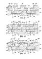
- FIGS. 1A through 1Gare partial cross-sectional views illustrating fabrication of an interconnect structure according to a first embodiment of the present invention.
- wires 100are formed in a first interconnect level 105 .
- Wires 100include conductive liners 110 and core conductors 115 .
- core conductors 110are copper and conductive liners 115 comprise a dual layer of tantalum and tantalum nitride, with the tantalum layer between the copper and the tantalum nitride layer.
- wires 100may be stud (formed from, for example as tungsten) which connect to devices, such as transistors, formed in a silicon layer (not shown) under first interconnect level 105 .
- First interconnect level 105includes a dielectric layer 120 (in which wires 100 are embedded) and a capping layer 125 in contact with and covering wires 100 and dielectric layer 120 .
- Capping layer 125may act as a copper diffusion barrier.
- dielectric layer 120is a low dielectric constant (low K) material, examples of which include but are not limited to hydrogen silsesquioxane polymer (HSQ), methyl silsesquioxane polymer (MSQ), SiLKTM (poly(arylene) ether) manufactured by Dow Chemical, Midland, Tex., BLACK DIAMONDTM (methyl doped silica) or (SiO x (CH3) y ) or (SiC x OyH z ) or (SiCOH) manufactured by Applied Materials, Santa Clara, Calif.
- HSQhydrogen silsesquioxane polymer
- MSQmethyl silsesquioxane polymer
- SiLKTMpoly(arylene) ether
- Dielectric layer 120may be, for example, between about 300 nm to about 2,000 nm thick.
- Examples of capping layer 125 materialsinclude but are not limited to silicon nitride (SiN), silicon carbide (SiC), silicon oxynitride (SiON), silicon carbo nitride (SiCN) and silicon oxycarbide (SiOC).
- Capping layer 120may be, for example, about 5 nm to about 200 nm thick.
- Second interconnect level 130includes a dielectric layer 135 formed on capping layer 125 and a capping layer 140 in contact with and covering dielectric layer 135 .
- the materials and thicknesses of dielectric layer 135may be any of the materials and thickness listed supra for dielectric layer 120 and the materials and thicknesses of capping layer 140 may be any of the materials and thickness listed supra for capping layer 125 .
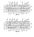
- wire trenches 145are formed completely through capping layer 140 and partially through dielectric layer 135 by any number of reactive ion etch (RIE) processes known in the art.
- a conformal sacrificial layer 150comprises formed on the sidewalls and bottoms of wire trenches 145 and exposed capping layer 140 .
- sacrificial layer 150comprises SiO 2 formed by plasma enhanced chemical vapor deposition (PECVD) and is between about 5 nm to about 300 nm thick.
- a photoresist layer 155is formed over sacrificial layer 150 and openings 160 formed in the photoresist layer exposing the sacrificial layer in the bottom of the openings.
- the thus exposed sacrificial layer 150comprises removed by selective RIE etching from the bottom of openings 160 to expose dielectric layer 135 .
- dielectric layer 135comprises SiLKTM
- sacrificial layer 150comprises SiO 2
- sacrificial layer 150may be RIE etched using CF 4 or other another F based gas, which selectively etches SiO 2 over SiLKTM.
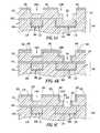
- resist layer 155(see FIG. 1C ) is removed and via openings 165 formed by selective RIE through remaining dielectric layer 135 and capping layer 125 to expose wires 100 in the bottom of the via openings.
- dielectric layer 135may be RIE etched using O 2 , N 2 , H 2 or a mixture thereof, which selectively etches SiLKTM over SiC.
- dielectric layer 135comprises SiCOH, dielectric layer 135 may be RIE etched using CF 4 .
- Wires 170are formed.
- Wires 170include core conductors 175 and conductive liners 180 .
- core conductors 175are copper and conductive liners 180 comprise a dual layer of tantalum and tantalum nitride, with the tantalum layer between the copper and the tantalum nitride layer.
- Wires 170may be formed by physical vapor deposition (PVD) of TaN, PVD of Ta, sputtering a thin layer of copper, plating a thick layer of copper, and performing a CMP to remove excess TaN, Ta, and copper using capping layer 140 as a polishing stop. Sacrificial layer 150 on top of capping layer 140 is also removed during the CMP. Note, that portions of sacrificial layer 150 are exposed at a surface 185 created by the CMP process.
- sacrificial layer 150is recess etched below surface 185 to expose sidewalls 190 of wires 170 and form air-gaps 195 having a width W 1 .
- Air gaps 195each include a first air-gap between capping layer 140 and wires 170 and a contiguous second air-gap between dielectric layer 135 and wires 170 , both the first and second air-gaps having about the same width W 1 .
- sacrificial layer 150comprises SiO 2 , either an aqueous HF etch or a RIE using, for example CF4, may be used to etch sacrificial layer 150 .
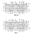
- a sealing layer 200is formed over surface 185 , sealing air-gaps 195 .
- Sealing layer 200may be about (W 1 divided by 2) or greater thick to ensure capping layer bridging between capping layer 140 and wires 170 .
- Sealing layer 200may be made from any of the materials indicated supra for capping layer 140 or capping layer 125 .
- capping layer 140is supported by pillars 202 of dielectric layer 135 . Also, there are un-etched sections of sacrificial layer 150 under wires 170 .
- FIGS. 2A and 2Bare partial cross-sectional views illustrating fabrication of an interconnect structure according to a second embodiment of the present invention. Since the effectiveness of air-gaps reducing RC delay is a function of the value of W 1 (see FIG. 1F ), the larger W 1 , the more effective the reduction.
- FIG. 2Auses the structure of FIG. 1F as an immediately previous step.
- dielectric layer 135is isotropically etched to increase the width of air-gaps 195 from W 1 (see FIG. 1F ) to form extended air-gaps 205 .
- Extended air gaps 205each include a first air-gap between capping layer 140 and wires 170 and a contiguous second air-gap between dielectric layer 135 and wires 170 , the first air-gaps having widths of about W 1 and the second air-gaps having widths of about W 2 , where W 2 >W 1 .
- dielectric layer 135comprises SiLKTM
- an exemplary etch processis a high pressure, low bias voltage RIE using O 2 , N 2 , H 2 or a combination thereof.
- sealing layer 200is formed over surface 185 , sealing air-gaps 205 .
- capping layer 140is supported by pillars 206 of dielectric layer 135 .
- FIGS. 3A through 3Gare partial cross-sectional views illustrating fabrication of an interconnect structure according to a third embodiment of the present invention.
- FIG. 3Auses the structure of FIG. 1B as an immediately previous step.
- an angled ion implant of species Xis performed into layer 150 , converting portions of sacrificial layer 150 to a sacrificial layer 215 wherever sacrificial layer 150 not shadowed by corners 220 of sacrificial layer 150 formed on corners of trenches 145 .
- sacrificial layer 150comprises SIO 2 and the implanted species X is N at a dose of about 1E 14 atm/cm 2 to about 1E 17 atm/cm 2 , then sacrificial layer 215 comprises SiON containing about 1% to about 50% N.
- sacrificial layer 150comprises SIO 2 and the implanted species X is C at a dose of about 1E 14 atm/cm 2 to about 1E 17 atm/cm 2
- sacrificial layer 215comprises SiOC containing about 1% to about 50% C.
- a photoresist layer 155is formed over sacrificial layers 150 and 215 and openings 160 formed in the photoresist layer exposing sacrificial layer 150 and/or sacrificial layer 215 in the bottom of the openings.
- the thus exposed sacrificial layer 150 and/or sacrificial layer 215comprises removed by selective RIE etching from the bottom of openings 160 to expose dielectric layer 135 . Then resist layer 155 (see FIG. 3B ) is removed and via openings 165 formed through remaining dielectric layer 135 and capping layer 125 to expose wires 100 in the bottom of the via openings.
- Wires 170are formed.
- Wires 170include core conductors 175 and conductive liners 180 as described supra.
- exposed portions of sacrificial layer 215are recess etched below surface 185 to expose sidewalls 190 of wires 170 and form air-gaps 195 .
- sacrificial layer 150comprises SiO 2 and sacrificial layer 215 comprises SiON
- an RIE etch using CF 4 and O 2may be used to etch sacrificial layer 215 selectively to sacrificial layer 150 .
- dielectric layer 135comprises isotropically etched to increase the width of air-gaps 195 thus forming extended air-gaps 210 .
- Extended air gaps 210each include a first air-gap between capping layer 140 and wires 170 and a contiguous second air-gap between dielectric layer 135 and wires 170 , the first air-gaps having less than the width of the second air-gap.
- Portions of sacrificial layer 150remain attached to portions of wires 170 and support capping layer 140 .
- sealing layer 200is formed over surface 185 , sealing air-gaps 210 . Note, there are un-etched sections of sacrificial layer 150 under wires 170 .
- FIGS. 4A through 4Kare partial cross-sectional views illustrating fabrication of an interconnect structure according to a fourth embodiment of the present invention.
- wires 100are formed in first interconnect level 105 .
- Wires 100include core conductors 115 and conductive liners 110 .
- First interconnect level 105includes dielectric layer 120 (in which wires 100 are embedded) and capping layer 125 in contact with and covering wires 100 and dielectric layer 120 .
- Formed top of first interconnect level 105is a second interconnect level 130 A.
- Second interconnect levelincludes a lower dielectric layer 135 A formed on capping layer 125 , an upper dielectric layer 135 B formed on lower dielectric layer 135 A and a capping layer 140 in contact with and covering upper dielectric layer 135 B.
- Lower and upper dielectric layers 135 A and 135 Bare different low K materials, examples of which include but are not limited to HSQ, MSQ, SiLKTM and SiCOH.
- lower dielectric layer 135 Acomprises SiCOH between about 200 nm to about 1,500 nm thick
- upper dielectric layer 135 Bcomprises SiLKTM between about 200 nm to about thick 1,500 nm
- capping layer 140comprises SiC between about 5 nm to about 200 nm thick.
- wire trenches 145are formed completely through capping layer 140 and completely through upper dielectric layer 135 B by any number of reactive ion etch (RIE) processes known in the art.
- RIE processesmay be chosen so upper dielectric layer 135 B comprises etched selectively to lower dielectric layer 135 A.
- upper dielectric layer 135 Bcomprises SiLKTM and lower dielectric layer 135 A comprises SiCOH
- an exemplary etch process for upper dielectric layer 135 Bcomprises a high pressure, low bias voltage RIE using O 2 , N 2 , H 2 or a combination thereof.
- sacrificial layer 150comprises formed on the sidewalls and bottoms of wire trenches 145 and exposed capping layer 140 .
- sacrificial layer 150comprises SiO 2 formed by plasma enhanced chemical vapor deposition (PECVD) and is between about 5 nm to about 300 nm thick.
- PECVDplasma enhanced chemical vapor deposition
- photoresist layer 155is formed over sacrificial layer 150 and openings 160 formed in the photoresist layer exposing the sacrificial layer in the bottom of the openings.
- FIG. 4Ethe thus exposed sacrificial layer 150 , lower dielectric later 135 A and capping layer 125 are removed by RIE etching from the bottom of openings 160 (see FIG. 4D ) to expose lower dielectric layer 135 A. Then resist layer 155 (see FIG. 4D ) is removed and via openings 165 formed through lower dielectric layer 135 A and capping layer 125 to expose wires 100 in the bottom of the via openings.
- wires 170are formed, wires 170 including core conductors 175 and conductive liners 180 , as described supra.
- Sacrificial layer 150 on top of capping layer 140is also removed during the CMP. Note, that portions of sacrificial layer 150 are exposed at a surface 185 created by the CMP process.
- a protective layer 225is formed on exposed top surfaces 230 of wires 170 .
- protective layer 225is electroless deposited cobalt tungsten phosphide (CoWP) about 5 nm to about 100 nm thick.
- a block copolymer layer 235is formed over protective layer 225 , exposed capping layer 140 and exposed sacrificial layer 150 .
- a block copolymeris a polymer containing alternating long sequences of two different polymers. Copolymer layer 235 is heated to drive of some or all of one polymer of the copolymer to form pores 240 in copolymer layer 235 . Wherever pores 240 exist in copolymer layer 235 , protective layer 225 , capping layer 140 and sacrificial layer 150 are exposed in the bottom of the pore.
- copolymer layer 235comprises a polymethylmethacrylate ⁇ PMMA) in polystyrene (PS) copolymer and heating to between about 100° C. to about 400° C. drives off the PMMA polymer or portions thereof.
- the PMMAcan be removed by use of a solvent that preferentially dissolves PMMA over PS.
- a top view of copolymer layer 235 with pores 240is given in FIG. 5 and described infra.
- a wet or RIE etchis performed to remove portions of sacrificial layer 150 exposed in the bottom of pores 240 .
- sacrificial layer 150being SiO 2
- an aqueous HF containing etchant or a CF4 RIE processmay be used.
- copolymer layer 235(see FIG. 4I ) is removed and upper dielectric layer 135 B (see FIG. 4I ) is removed using an isotropic etch selective to upper dielectric layer 135 B (see FIG. 4I ) over lower dielectric layer 135 A to form extended air-gaps 245 . All (as illustrated in FIG. 4J ) or some of upper dielectric layer 135 B may be removed. As illustrated, extended air gaps 245 each include a first air-gap between capping layer 140 and wires 170 and a contiguous second air-gap where upper dielectric layer 135 B (see FIG.
- upper dielectric layer 135 B(see FIG. 4I ) is SiLKTM and lower dielectric layer 135 A comprises SiCOH, a high-pressure RIE using O 2 , N 2 , H 2 or combinations thereof may be used.
- Capping layer 140is supported by attachment to sacrificial layer 150 .
- sealing layer 200is formed over surface 185 , sealing extended air-gaps 245 .
- FIG. 5is a top view illustrating the porosity of copolymer layer 235 as illustrated in FIG. 4H .
- stripes of sacrificial layer 150are spaced between either capping layer 150 or wires 170 and pores 240 randomly distributed in copolymer layer 235 . Wherever a pore overlaps sacrificial layer 150 , the sacrificial layer is exposed in the bottom of the pore and may be etched away.
- FIGS. 6A through 6Gare partial cross-sectional views illustrating fabrication of an interconnect structure according to a fifth embodiment of the present invention.
- wires 100are formed in first interconnect level 105 .
- Wires 100include core conductors 115 and conductive liners 110 .
- First interconnect level 105includes dielectric layer 120 (in which wires 100 are embedded) and capping layer 125 in contact with and covering wires 100 and dielectric layer 120 .
- Formed top of first interconnect level 105is dielectric layer 135 .
- Formed on top of dielectric layer 135comprises a hard mask layer 250 . Materials and thicknesses for wires 100 , dielectric layers 120 and 135 and capping layer 125 have been discussed supra.
- Hard mask layermay be formed from SiO 2 , SiN, SiC, SiOC or SiON.
- wire trenches 145 A and 145 BFormed through hard mask layer 250 and part way through dielectric layer 135 are wire trenches 145 A and 145 B and formed in the bottom of wire trench 145 B through the remaining thickness of dielectric layer 135 and through capping layer 125 comprises via opening 165 .
- a wire 100is exposed on the bottom of via opening 165 .
- a conformal sacrificial layer 255is formed covering a top surface 260 of hard mask layer 250 and the sidewalls and bottom of wire trenches 145 A and 145 B and via opening 165 .
- sacrificial layer 255is tungsten and is about 5 nm to about 300 nm thick.
- an RIE processis performed to remove tungsten from top surface 260 of hard mask layer 250 and the bottoms of wire trenches 145 A and 145 B and via opening 165 leaving spacers 265 on the sidewalls of the wire trenches and via opening.
- dielectric layer 135comprises SiLKTM
- the RIE processmay use CF4 and O 2 with a high bias voltage which selectively etches tungsten over SiLKTM.
- the structure illustrated in FIG. 6Ccan be formed directly from the structure illustrated in FIG. 6A , by direct deposition of tungsten on the sidewalls of wire trenches 145 A and 145 B and via opening 165 using ionized plasma PVD tuned for a high sputter rate.
- wires 170including core conductors 175 and conductive liners 180 , are formed as described supra.
- Air gaps 270each include a first air-gap between capping layer 140 and wires 170 and a contiguous second air-gap between dielectric layer 135 and wires 170 , both the first and second air-gaps having about the same width. Any etch process known in the art that will etch tungsten but not wires 170 may be used.
- dielectric layer 135is isotropically etched to form extended air-gaps 275 under hard mask layer 250 adjacent to wires 170 .
- Extended air gaps 275each include a first air-gap between capping layer 140 and wires 170 and a contiguous second air-gap between dielectric layer 135 and wires 170 , the first air-gaps having widths less than widths of the second air-gaps.
- dielectric layer 135may be RIE etched using O 2 , N 2 , H 2 or a mixture thereof, which selectively etches SiLKTM over SiC.
- capping layer 200is formed (as described supra) over hard mask layer 250 sealing extended air-gaps 275 . Note, pillars 285 of dielectric layer 135 remain in contact with a bottom surface of wires 170 .
- FIG. 7is a partial cross-section illustrating an air-gap extending under wires 170 .
- extended air-gaps 280are formed which extend under wires 170 , but pillars 290 of dielectric layer 135 remain in contact with a bottom surface of wires 170 (where there is not an integral via as described supra).
- Over etch of dielectric layer 135may be applied to all embodiments of the present invention to extend the various air-gaps under wires 170 except the fourth embodiment.
- the present inventionprovides interconnection structures and methods of fabricating interconnection structures that are less sensitive to RC delay.
- first, second, third and fifth embodiments of the present inventionmay be adapted to utilize the dual layers of dielectric of the fourth embodiment of the present invention, including the dual layer comprising SiLKTM over SiCOH. Therefore, it is intended that the following claims cover all such modifications and changes as fall within the true spirit and scope of the invention.
Landscapes
- Engineering & Computer Science (AREA)
- Physics & Mathematics (AREA)
- Condensed Matter Physics & Semiconductors (AREA)
- General Physics & Mathematics (AREA)
- Computer Hardware Design (AREA)
- Microelectronics & Electronic Packaging (AREA)
- Power Engineering (AREA)
- Manufacturing & Machinery (AREA)
- Internal Circuitry In Semiconductor Integrated Circuit Devices (AREA)
Abstract
Description
- This Application is a divisional of U.S. patent application Ser. No. 10/711,394 filed on Sep. 16, 2004.
- The present invention relates to the field of integrated circuits; more specifically, it relates to air-gap insulated interconnection structures and methods of fabricating air-gap insulated interconnection structures for integrated circuits.
- Integrated circuits comprise active components such as transistors formed in a semiconductor substrate that are wired together to form integrated circuits. The wiring together is accomplished in interconnect levels. Interconnect levels include electrically conductive lines embedded in a dielectric layer with vias connecting the conductive wires in a particular interconnect level to conductive wires in higher or lower interconnect levels or to the active devices.
- As integrated circuit size decreases and density increases, the distance between these conductive lines, especially in the same level, decreases. As the spacing between adjacent conductive lines decreases, the resistive-capacitive (RC) coupling induced in one line by a signal in an adjacent line increases, often to the point of negating increases in performance expected by increasing conductive wire density.
- Therefore, there is a need for interconnection structures and methods of fabricating interconnection structures that are less sensitive to RC delay.
- A first aspect of the present invention is a method, comprising: forming a dielectric layer on a substrate; forming a capping layer on a top surface of the dielectric layer; forming a trench through the capping layer, the trench extending toward the substrate and into but not through, the dielectric layer; forming a sacrificial layer on opposing sidewalls of the trench; filling the trench with a electrical conductor; and removing a portion of the sacrificial layer from between the electrical conductor and the dielectric layer to form air-gaps.
- A second aspect of the present invention is a structure, comprising: a dielectric layer on a substrate; the capping layer formed on a top surface of the dielectric layer; a damascene or dual damascene wire extending below the top surface of the dielectric layer, a top surface of the damascene or dual damascene wire coplanar with a top surface of a capping layer; a first air-gap between sidewalls of the a damascene or dual damascene wire and the capping layer and a second air-gap between the sidewalls of the damascene or dual damascene wire and the dielectric layer, the first air-gap and the second air gap contiguous to each other; and a sealing layer on the top surface of the damascene or dual damascene wire and the top surface of the capping layer, the sealing layer bridging across and sealing a top of the first air-gap.
- The features of the invention are set forth in the appended claims. The invention itself, however, will be best understood by reference to the following detailed description of an illustrative embodiment when read in conjunction with the accompanying drawings, wherein:
FIGS. 1A through 1G are partial cross-sectional views illustrating fabrication of an interconnect structure according to a first embodiment of the present invention;FIGS. 2A and 2B are partial cross-sectional views illustrating fabrication of an interconnect structure according to a second embodiment of the present invention;FIGS. 3A through 3G are partial cross-sectional views illustrating fabrication of an interconnect structure according to a third embodiment of the present invention;FIGS. 4A through 4K are partial cross-sectional views illustrating fabrication of an interconnect structure according to a fourth embodiment of the present invention;FIG. 5 is a top view illustrating the porosity ofcopolymer layer 235 as illustrated inFIG. 4H ;FIGS. 6A through 6G are partial cross-sectional views illustrating fabrication of an interconnect structure according to a fifth embodiment of the present invention; andFIG. 7 is a partial cross-section illustrating an air-gap extending under conductive lines.- The present invention utilizes interconnect structures formed by damascene and dual damascene processes. A damascene process is one in which wire trench or via openings are formed in a dielectric layer, an electrical conductor deposited on a top surface of the dielectric of sufficient thickness to fill the trenches and a chemical-mechanical-polish (CMP) process performed to remove excess conductor and make the surface of the conductor co-planer with the surface of the dielectric layer to form a damascene wires (or damascene vias).
- A dual damascene process is one in which via openings are formed through the entire thickness of a dielectric layer followed by formation of trenches part of the way through the dielectric layer in any given cross-sectional view. All via openings are intersected by integral wire trenches above and by a wire trench below, but not all trenches need intersect a via opening. An electrical conductor is deposited on a top surface of the dielectric of sufficient thickness to fill the trenches and via opening and a CMP process performed to make the surface of the conductor in the trench co-planer with the surface the dielectric layer to form dual damascene wire and dual damascene wires having integral dual damascene vias. For the purposes of the present invention the term wire is equivalent to the terms damascene and dual damascene wire unless otherwise stated.
- Reduction of RC delay (which is a function of the dielectric constant of the dielectric material between the wires, the lower the dielectric constant, the lower the RC delay) is accomplished in the present invention by the use of a sacrificial sidewall layer around wires which can be removed forming air-gaps and provide access to the dielectric layer which can be removed to form wider or extended air-gaps in the dielectric layer between wires on the same interconnect level. The RC delay is reduced because air has a lower dielectric constant than most solid dielectric materials.
- For the purposes of the present invention, the term air-gap includes enclosed voids filled with air, inert gases or partial vacuums containing air or inert gases. The term gap implies an opening in a layer filled with the ambient atmosphere.
FIGS. 1A through 1G are partial cross-sectional views illustrating fabrication of an interconnect structure according to a first embodiment of the present invention. InFIG. 1A ,wires 100 are formed in afirst interconnect level 105.Wires 100 includeconductive liners 110 andcore conductors 115. In oneexample core conductors 110 are copper andconductive liners 115 comprise a dual layer of tantalum and tantalum nitride, with the tantalum layer between the copper and the tantalum nitride layer. Alternatively,wires 100 may be stud (formed from, for example as tungsten) which connect to devices, such as transistors, formed in a silicon layer (not shown) underfirst interconnect level 105.First interconnect level 105 includes a dielectric layer120 (in whichwires 100 are embedded) and acapping layer 125 in contact with and coveringwires 100 anddielectric layer 120.Capping layer 125 may act as a copper diffusion barrier. In one exampledielectric layer 120 is a low dielectric constant (low K) material, examples of which include but are not limited to hydrogen silsesquioxane polymer (HSQ), methyl silsesquioxane polymer (MSQ), SiLK™ (poly(arylene) ether) manufactured by Dow Chemical, Midland, Tex., BLACK DIAMOND™ (methyl doped silica) or (SiOx(CH3)y) or (SiCxOyHz) or (SiCOH) manufactured by Applied Materials, Santa Clara, Calif. for which SiCOH will be hereafter. For the purposes of the present invention, a low K material is defined as a material having a lower dielectric constant than that of undoped thermal SiO2.Dielectric layer 120 may be, for example, between about 300 nm to about 2,000 nm thick. Examples ofcapping layer 125 materials include but are not limited to silicon nitride (SiN), silicon carbide (SiC), silicon oxynitride (SiON), silicon carbo nitride (SiCN) and silicon oxycarbide (SiOC).Capping layer 120 may be, for example, about 5 nm to about 200 nm thick.- Formed on top of
first interconnect level 105 is asecond interconnect level 130. Second interconnect level includes adielectric layer 135 formed oncapping layer 125 and acapping layer 140 in contact with and coveringdielectric layer 135. The materials and thicknesses ofdielectric layer 135 may be any of the materials and thickness listed supra fordielectric layer 120 and the materials and thicknesses ofcapping layer 140 may be any of the materials and thickness listed supra forcapping layer 125. - In
FIG. 1B ,wire trenches 145 are formed completely throughcapping layer 140 and partially throughdielectric layer 135 by any number of reactive ion etch (RIE) processes known in the art. A conformalsacrificial layer 150 comprises formed on the sidewalls and bottoms ofwire trenches 145 and exposedcapping layer 140. In one example,sacrificial layer 150 comprises SiO2formed by plasma enhanced chemical vapor deposition (PECVD) and is between about 5 nm to about 300 nm thick. - In
FIG. 1C , aphotoresist layer 155 is formed oversacrificial layer 150 andopenings 160 formed in the photoresist layer exposing the sacrificial layer in the bottom of the openings. The thus exposedsacrificial layer 150 comprises removed by selective RIE etching from the bottom ofopenings 160 to exposedielectric layer 135. For example, ifdielectric layer 135 comprises SiLK™ andsacrificial layer 150 comprises SiO2,sacrificial layer 150 may be RIE etched using CF4or other another F based gas, which selectively etches SiO2over SiLK™. - In
FIG. 1D , resist layer155 (seeFIG. 1C ) is removed and viaopenings 165 formed by selective RIE through remainingdielectric layer 135 andcapping layer 125 to exposewires 100 in the bottom of the via openings. In one example, ifdielectric layer 135 comprises SiLK™ andcapping layer 125 comprises SiC,dielectric layer 135 may be RIE etched using O2, N2, H2or a mixture thereof, which selectively etches SiLK™ over SiC. Ifdielectric layer 135 comprises SiCOH,dielectric layer 135 may be RIE etched using CF4. - In
FIG. 1E ,wires 170 are formed.Wires 170 includecore conductors 175 andconductive liners 180. In oneexample core conductors 175 are copper andconductive liners 180 comprise a dual layer of tantalum and tantalum nitride, with the tantalum layer between the copper and the tantalum nitride layer.Wires 170 may be formed by physical vapor deposition (PVD) of TaN, PVD of Ta, sputtering a thin layer of copper, plating a thick layer of copper, and performing a CMP to remove excess TaN, Ta, and copper usingcapping layer 140 as a polishing stop.Sacrificial layer 150 on top of cappinglayer 140 is also removed during the CMP. Note, that portions ofsacrificial layer 150 are exposed at asurface 185 created by the CMP process. - In
FIG. 1F , exposed portions ofsacrificial layer 150 are recess etched belowsurface 185 to exposesidewalls 190 ofwires 170 and form air-gaps 195 having a width W1.Air gaps 195 each include a first air-gap between cappinglayer 140 andwires 170 and a contiguous second air-gap betweendielectric layer 135 andwires 170, both the first and second air-gaps having about the same width W1. Ifsacrificial layer 150 comprises SiO2, either an aqueous HF etch or a RIE using, for example CF4, may be used to etchsacrificial layer 150. - In
FIG. 1G , asealing layer 200 is formed oversurface 185, sealing air-gaps 195.Sealing layer 200 may be about (W1 divided by 2) or greater thick to ensure capping layer bridging between cappinglayer 140 andwires 170.Sealing layer 200 may be made from any of the materials indicated supra for cappinglayer 140 orcapping layer 125. Note thatcapping layer 140 is supported by pillars202 ofdielectric layer 135. Also, there are un-etched sections ofsacrificial layer 150 underwires 170. FIGS. 2A and 2B are partial cross-sectional views illustrating fabrication of an interconnect structure according to a second embodiment of the present invention. Since the effectiveness of air-gaps reducing RC delay is a function of the value of W1 (seeFIG. 1F ), the larger W1, the more effective the reduction.FIG. 2A uses the structure ofFIG. 1F as an immediately previous step. InFIG. 2A ,dielectric layer 135 is isotropically etched to increase the width of air-gaps 195 from W1 (seeFIG. 1F ) to form extended air-gaps 205.Extended air gaps 205 each include a first air-gap between cappinglayer 140 andwires 170 and a contiguous second air-gap betweendielectric layer 135 andwires 170, the first air-gaps having widths of about W1 and the second air-gaps having widths of about W2, where W2>W1. Ifdielectric layer 135 comprises SiLK™, an exemplary etch process is a high pressure, low bias voltage RIE using O2, N2, H2or a combination thereof.- In
FIG. 2B , sealinglayer 200 is formed oversurface 185, sealing air-gaps 205. Note thatcapping layer 140 is supported bypillars 206 ofdielectric layer 135. Also, there are un-etched sections ofsacrificial layer 150 underwires 170. FIGS. 3A through 3G are partial cross-sectional views illustrating fabrication of an interconnect structure according to a third embodiment of the present invention.FIG. 3A uses the structure ofFIG. 1B as an immediately previous step. InFIG. 3A , an angled ion implant of species X is performed intolayer 150, converting portions ofsacrificial layer 150 to asacrificial layer 215 whereversacrificial layer 150 not shadowed bycorners 220 ofsacrificial layer 150 formed on corners oftrenches 145. In a first example, ifsacrificial layer 150 comprises SIO2and the implanted species X is N at a dose of about 1E14atm/cm2to about 1E17atm/cm2, thensacrificial layer 215 comprises SiON containing about 1% to about 50% N. In a second example, ifsacrificial layer 150 comprises SIO2and the implanted species X is C at a dose of about 1E14atm/cm2to about 1E17atm/cm2, thensacrificial layer 215 comprises SiOC containing about 1% to about 50% C.- In
FIG. 3B , aphotoresist layer 155 is formed oversacrificial layers openings 160 formed in the photoresist layer exposingsacrificial layer 150 and/orsacrificial layer 215 in the bottom of the openings. - In
FIG. 3C , the thus exposedsacrificial layer 150 and/orsacrificial layer 215 comprises removed by selective RIE etching from the bottom ofopenings 160 to exposedielectric layer 135. Then resist layer155 (seeFIG. 3B ) is removed and viaopenings 165 formed through remainingdielectric layer 135 andcapping layer 125 to exposewires 100 in the bottom of the via openings. - In
FIG. 3D ,wires 170 are formed.Wires 170 includecore conductors 175 andconductive liners 180 as described supra. - In
FIG. 3E , exposed portions ofsacrificial layer 215 are recess etched belowsurface 185 to exposesidewalls 190 ofwires 170 and form air-gaps 195. In the example thatsacrificial layer 150 comprises SiO2andsacrificial layer 215 comprises SiON, an RIE etch using CF4and O2may be used to etchsacrificial layer 215 selectively tosacrificial layer 150. - In
FIG. 3F ,dielectric layer 135 comprises isotropically etched to increase the width of air-gaps 195 thus forming extended air-gaps 210.Extended air gaps 210 each include a first air-gap between cappinglayer 140 andwires 170 and a contiguous second air-gap betweendielectric layer 135 andwires 170, the first air-gaps having less than the width of the second air-gap. Portions ofsacrificial layer 150 remain attached to portions ofwires 170 andsupport capping layer 140. - In
FIG. 3G , sealinglayer 200 is formed oversurface 185, sealing air-gaps 210. Note, there are un-etched sections ofsacrificial layer 150 underwires 170. FIGS. 4A through 4K are partial cross-sectional views illustrating fabrication of an interconnect structure according to a fourth embodiment of the present invention. InFIG. 4A ,wires 100 are formed infirst interconnect level 105.Wires 100 includecore conductors 115 andconductive liners 110.First interconnect level 105 includes dielectric layer120 (in whichwires 100 are embedded) andcapping layer 125 in contact with and coveringwires 100 anddielectric layer 120. Formed top offirst interconnect level 105 is asecond interconnect level 130A. Second interconnect level includes a lowerdielectric layer 135A formed on cappinglayer 125, anupper dielectric layer 135B formed on lowerdielectric layer 135A and acapping layer 140 in contact with and coveringupper dielectric layer 135B. Lower and upperdielectric layers dielectric layer 135A comprises SiCOH between about 200 nm to about 1,500 nm thick,upper dielectric layer 135B comprises SiLK™ between about 200 nm to about thick 1,500 nm andcapping layer 140 comprises SiC between about 5 nm to about 200 nm thick.- In
FIG. 4B ,wire trenches 145 are formed completely through cappinglayer 140 and completely throughupper dielectric layer 135B by any number of reactive ion etch (RIE) processes known in the art. RIE processes may be chosen so upperdielectric layer 135B comprises etched selectively to lowerdielectric layer 135A. In the example thatupper dielectric layer 135B comprises SiLK™ and lowerdielectric layer 135A comprises SiCOH, an exemplary etch process for upperdielectric layer 135B comprises a high pressure, low bias voltage RIE using O2, N2, H2or a combination thereof. - In
FIG. 4C ,sacrificial layer 150 comprises formed on the sidewalls and bottoms ofwire trenches 145 and exposedcapping layer 140. In one example,sacrificial layer 150 comprises SiO2formed by plasma enhanced chemical vapor deposition (PECVD) and is between about 5 nm to about 300 nm thick. - In
FIG. 4D ,photoresist layer 155 is formed oversacrificial layer 150 andopenings 160 formed in the photoresist layer exposing the sacrificial layer in the bottom of the openings. - In
FIG. 4E , the thus exposedsacrificial layer 150, lower dielectric later135A andcapping layer 125 are removed by RIE etching from the bottom of openings160 (seeFIG. 4D ) to expose lowerdielectric layer 135A. Then resist layer155 (seeFIG. 4D ) is removed and viaopenings 165 formed through lowerdielectric layer 135A andcapping layer 125 to exposewires 100 in the bottom of the via openings. - In
FIG. 4F ,wires 170 are formed,wires 170 includingcore conductors 175 andconductive liners 180, as described supra.Sacrificial layer 150 on top of cappinglayer 140 is also removed during the CMP. Note, that portions ofsacrificial layer 150 are exposed at asurface 185 created by the CMP process. - In
FIG. 4G , aprotective layer 225 is formed on exposedtop surfaces 230 ofwires 170. In one example,protective layer 225 is electroless deposited cobalt tungsten phosphide (CoWP) about 5 nm to about 100 nm thick. - In
FIG. 4H ablock copolymer layer 235 is formed overprotective layer 225, exposed cappinglayer 140 and exposedsacrificial layer 150. A block copolymer is a polymer containing alternating long sequences of two different polymers.Copolymer layer 235 is heated to drive of some or all of one polymer of the copolymer to formpores 240 incopolymer layer 235. Wherever pores240 exist incopolymer layer 235,protective layer 225, cappinglayer 140 andsacrificial layer 150 are exposed in the bottom of the pore. In oneexample copolymer layer 235 comprises a polymethylmethacrylate {PMMA) in polystyrene (PS) copolymer and heating to between about 100° C. to about 400° C. drives off the PMMA polymer or portions thereof. Alternatively, the PMMA can be removed by use of a solvent that preferentially dissolves PMMA over PS. A top view ofcopolymer layer 235 withpores 240 is given inFIG. 5 and described infra. - In
FIG. 4I , a wet or RIE etch is performed to remove portions ofsacrificial layer 150 exposed in the bottom ofpores 240. In the example ofsacrificial layer 150 being SiO2, an aqueous HF containing etchant or a CF4 RIE process may be used. - In
FIG. 4J , copolymer layer235 (seeFIG. 4I ) is removed andupper dielectric layer 135B (seeFIG. 4I ) is removed using an isotropic etch selective toupper dielectric layer 135B (seeFIG. 4I ) over lowerdielectric layer 135A to form extended air-gaps 245. All (as illustrated inFIG. 4J ) or some of upperdielectric layer 135B may be removed. As illustrated,extended air gaps 245 each include a first air-gap between cappinglayer 140 andwires 170 and a contiguous second air-gap whereupper dielectric layer 135B (seeFIG. 4I ) existed before it was etched away, the first air-gaps having widths less than widths of the second air-gap. In the example thatupper dielectric layer 135B (seeFIG. 4I ) is SiLK™ and lowerdielectric layer 135A comprises SiCOH, a high-pressure RIE using O2, N2, H2or combinations thereof may be used. Cappinglayer 140 is supported by attachment tosacrificial layer 150. - In
FIG. 4K , sealinglayer 200 is formed oversurface 185, sealing extended air-gaps 245. FIG. 5 is a top view illustrating the porosity ofcopolymer layer 235 as illustrated inFIG. 4H . InFIG. 5 , stripes ofsacrificial layer 150 are spaced between either cappinglayer 150 orwires 170 andpores 240 randomly distributed incopolymer layer 235. Wherever a pore overlapssacrificial layer 150, the sacrificial layer is exposed in the bottom of the pore and may be etched away.FIGS. 6A through 6G are partial cross-sectional views illustrating fabrication of an interconnect structure according to a fifth embodiment of the present invention. InFIG. 6A ,wires 100 are formed infirst interconnect level 105.Wires 100 includecore conductors 115 andconductive liners 110.First interconnect level 105 includes dielectric layer120 (in whichwires 100 are embedded) andcapping layer 125 in contact with and coveringwires 100 anddielectric layer 120. Formed top offirst interconnect level 105 isdielectric layer 135. Formed on top ofdielectric layer 135 comprises ahard mask layer 250. Materials and thicknesses forwires 100,dielectric layers capping layer 125 have been discussed supra. Hard mask layer may be formed from SiO2, SiN, SiC, SiOC or SiON. Formed throughhard mask layer 250 and part way throughdielectric layer 135 arewire trenches wire trench 145B through the remaining thickness ofdielectric layer 135 and through cappinglayer 125 comprises viaopening 165. Awire 100 is exposed on the bottom of viaopening 165.- In
FIG. 6B , a conformalsacrificial layer 255 is formed covering a top surface260 ofhard mask layer 250 and the sidewalls and bottom ofwire trenches opening 165. In one examplesacrificial layer 255 is tungsten and is about 5 nm to about 300 nm thick. - In
FIG. 6C , an RIE process is performed to remove tungsten from top surface260 ofhard mask layer 250 and the bottoms ofwire trenches opening 165 leavingspacers 265 on the sidewalls of the wire trenches and via opening. In the example thatdielectric layer 135 comprises SiLK™, the RIE process may use CF4 and O2with a high bias voltage which selectively etches tungsten over SiLK™. Alternatively, the structure illustrated inFIG. 6C can be formed directly from the structure illustrated inFIG. 6A , by direct deposition of tungsten on the sidewalls ofwire trenches opening 165 using ionized plasma PVD tuned for a high sputter rate. - In
FIG. 6D ,wires 170, includingcore conductors 175 andconductive liners 180, are formed as described supra. - In
FIG. 6E , spacers265 (seeFIG. 6D ) are removed from the side ofwires 170 to form air-gaps 270 using, for example, an aqueous H2O2solution.Air gaps 270 each include a first air-gap between cappinglayer 140 andwires 170 and a contiguous second air-gap betweendielectric layer 135 andwires 170, both the first and second air-gaps having about the same width. Any etch process known in the art that will etch tungsten but notwires 170 may be used. - In
FIG. 6F ,dielectric layer 135 is isotropically etched to form extended air-gaps 275 underhard mask layer 250 adjacent towires 170.Extended air gaps 275 each include a first air-gap between cappinglayer 140 andwires 170 and a contiguous second air-gap betweendielectric layer 135 andwires 170, the first air-gaps having widths less than widths of the second air-gaps. In one example, ifdielectric layer 135 comprises SiLK™ andhard mask layer 250 comprises SiC,dielectric layer 135 may be RIE etched using O2, N2, H2or a mixture thereof, which selectively etches SiLK™ over SiC. - In
FIG. 6G , cappinglayer 200 is formed (as described supra) overhard mask layer 250 sealing extended air-gaps 275. Note,pillars 285 ofdielectric layer 135 remain in contact with a bottom surface ofwires 170. FIG. 7 is a partial cross-section illustrating an air-gap extending underwires 170. By overetching dielectric layer 135, extended air-gaps 280 are formed which extend underwires 170, butpillars 290 ofdielectric layer 135 remain in contact with a bottom surface of wires170 (where there is not an integral via as described supra). Over etch ofdielectric layer 135 may be applied to all embodiments of the present invention to extend the various air-gaps underwires 170 except the fourth embodiment.- Thus the present invention provides interconnection structures and methods of fabricating interconnection structures that are less sensitive to RC delay.
- The description of the embodiments of the present invention is given above for the understanding of the present invention. It will be understood that the invention is not limited to the particular embodiments described herein, but is capable of various modifications, rearrangements and substitutions as will now become apparent to those skilled in the art without departing from the scope of the invention. For example, the first, second, third and fifth embodiments of the present invention may be adapted to utilize the dual layers of dielectric of the fourth embodiment of the present invention, including the dual layer comprising SiLK™ over SiCOH. Therefore, it is intended that the following claims cover all such modifications and changes as fall within the true spirit and scope of the invention.
Claims (17)
Priority Applications (1)
| Application Number | Priority Date | Filing Date | Title |
|---|---|---|---|
| US11/772,899US7671442B2 (en) | 2004-09-16 | 2007-07-03 | Air-gap insulated interconnections |
Applications Claiming Priority (2)
| Application Number | Priority Date | Filing Date | Title |
|---|---|---|---|
| US10/711,394US7285474B2 (en) | 2004-09-16 | 2004-09-16 | Air-gap insulated interconnections |
| US11/772,899US7671442B2 (en) | 2004-09-16 | 2007-07-03 | Air-gap insulated interconnections |
Related Parent Applications (1)
| Application Number | Title | Priority Date | Filing Date |
|---|---|---|---|
| US10/711,394DivisionUS7285474B2 (en) | 2004-09-16 | 2004-09-16 | Air-gap insulated interconnections |
Publications (2)
| Publication Number | Publication Date |
|---|---|
| US20070252282A1true US20070252282A1 (en) | 2007-11-01 |
| US7671442B2 US7671442B2 (en) | 2010-03-02 |
Family
ID=36034613
Family Applications (2)
| Application Number | Title | Priority Date | Filing Date |
|---|---|---|---|
| US10/711,394Active2026-01-13US7285474B2 (en) | 2004-09-16 | 2004-09-16 | Air-gap insulated interconnections |
| US11/772,899Expired - LifetimeUS7671442B2 (en) | 2004-09-16 | 2007-07-03 | Air-gap insulated interconnections |
Family Applications Before (1)
| Application Number | Title | Priority Date | Filing Date |
|---|---|---|---|
| US10/711,394Active2026-01-13US7285474B2 (en) | 2004-09-16 | 2004-09-16 | Air-gap insulated interconnections |
Country Status (1)
| Country | Link |
|---|---|
| US (2) | US7285474B2 (en) |
Cited By (7)
| Publication number | Priority date | Publication date | Assignee | Title |
|---|---|---|---|---|
| US20080150152A1 (en)* | 2006-12-21 | 2008-06-26 | Commissariat A L'energie Atomique | Carbon nanotube-based interconnection element |
| US20080299766A1 (en)* | 2007-05-31 | 2008-12-04 | Seiichi Omoto | Method for fabricating semiconductor device |
| KR100922559B1 (en) | 2007-12-31 | 2009-10-21 | 주식회사 동부하이텍 | Semiconductor device and its manufacturing method |
| US20090325381A1 (en)* | 2008-06-27 | 2009-12-31 | Applied Materials, Inc. | Prevention and reduction of solvent and solution penetration into porous dielectrics using a thin barrier layer |
| CN103094186A (en)* | 2011-10-31 | 2013-05-08 | 中芯国际集成电路制造(上海)有限公司 | Semiconductor structure and forming method thereof |
| TWI813257B (en)* | 2021-11-17 | 2023-08-21 | 台灣積體電路製造股份有限公司 | Semiconductor device and formation method thereof |
| US20230352340A1 (en)* | 2020-07-30 | 2023-11-02 | Taiwan Semiconductor Manufacturing Company, Ltd. | Semiconductor device structure and methods of forming the same |
Families Citing this family (49)
| Publication number | Priority date | Publication date | Assignee | Title |
|---|---|---|---|---|
| DE102004003337A1 (en)* | 2004-01-22 | 2005-08-18 | Infineon Technologies Ag | Plasma enhanced chemical vapor deposition method, silicon-oxygen-nitrogen containing material and layer assembly |
| CN100356545C (en)* | 2004-09-21 | 2007-12-19 | 中芯国际集成电路制造(上海)有限公司 | Method and structure for lowering contact electric resistance in double inlay structure of semiconductor device |
| DE102004050391B4 (en)* | 2004-10-15 | 2007-02-08 | Infineon Technologies Ag | Method for producing a layer arrangement and layer arrangement |
| US7977032B2 (en)* | 2005-02-11 | 2011-07-12 | International Business Machines Corporation | Method to create region specific exposure in a layer |
| US7122898B1 (en)* | 2005-05-09 | 2006-10-17 | International Business Machines Corporation | Electrical programmable metal resistor |
| US7629225B2 (en)* | 2005-06-13 | 2009-12-08 | Infineon Technologies Ag | Methods of manufacturing semiconductor devices and structures thereof |
| US7485581B2 (en)* | 2005-11-30 | 2009-02-03 | Lam Research Corporation | Device with gaps for capacitance reduction |
| JP2008010534A (en)* | 2006-06-28 | 2008-01-17 | Sony Corp | Semiconductor device and manufacturing method thereof |
| US7803713B2 (en)* | 2006-09-21 | 2010-09-28 | Taiwan Semiconductor Manufacturing Co. Ltd. | Method for fabricating air gap for semiconductor device |
| US7488682B2 (en)* | 2006-10-03 | 2009-02-10 | International Business Machines Corporation | High-density 3-dimensional resistors |
| US20080119040A1 (en)* | 2006-11-21 | 2008-05-22 | Taiwan Semiconductor Manufacturing Co., Ltd. | Method for forming a dual damascene structure |
| US7723237B2 (en)* | 2006-12-15 | 2010-05-25 | Tokyo Electron Limited | Method for selective removal of damaged multi-stack bilayer films |
| JP5067068B2 (en)* | 2007-08-17 | 2012-11-07 | 東京エレクトロン株式会社 | Semiconductor device manufacturing method and storage medium |
| US20090072409A1 (en)* | 2007-09-14 | 2009-03-19 | International Business Machines Corporation | Interconnect Structures Incorporating Air-Gap Spacers |
| US20090079083A1 (en)* | 2007-09-26 | 2009-03-26 | United Microelectronics Corp. | Interconnect structure and fabricating method of the same |
| US8772156B2 (en)* | 2008-05-09 | 2014-07-08 | International Business Machines Corporation | Methods of fabricating interconnect structures containing various capping materials for electrical fuse and other related applications |
| US7956466B2 (en) | 2008-05-09 | 2011-06-07 | International Business Machines Corporation | Structure for interconnect structure containing various capping materials for electrical fuse and other related applications |
| US8279572B2 (en)* | 2008-06-23 | 2012-10-02 | International Business Machines Corporation | Structure for an on-chip high frequency electro-static discharge device |
| US8298911B2 (en)* | 2009-03-26 | 2012-10-30 | Samsung Electronics Co., Ltd. | Methods of forming wiring structures |
| KR101536333B1 (en)* | 2009-03-26 | 2015-07-14 | 삼성전자주식회사 | Wiring structure and Method of forming the same |
| US8003516B2 (en)* | 2009-08-26 | 2011-08-23 | International Business Machines Corporation | BEOL interconnect structures and related fabrication methods |
| US8456009B2 (en) | 2010-02-18 | 2013-06-04 | Taiwan Semiconductor Manufacturing Company, Ltd. | Semiconductor structure having an air-gap region and a method of manufacturing the same |
| US8030202B1 (en) | 2010-12-10 | 2011-10-04 | International Business Machines Corporation | Temporary etchable liner for forming air gap |
| US8754338B2 (en)* | 2011-05-28 | 2014-06-17 | Banpil Photonics, Inc. | On-chip interconnects with reduced capacitance and method of afbrication |
| US8643187B1 (en)* | 2011-06-01 | 2014-02-04 | Banpil Photonics, Inc. | On-chip interconnects VIAS and method of fabrication |
| DE102011083333A1 (en)* | 2011-09-23 | 2013-03-28 | Endress + Hauser Gmbh + Co. Kg | gauge |
| US8872349B2 (en) | 2012-09-11 | 2014-10-28 | Intel Corporation | Bridge interconnect with air gap in package assembly |
| US9059258B2 (en)* | 2013-03-04 | 2015-06-16 | International Business Machines Corporation | Controlled metal extrusion opening in semiconductor structure and method of forming |
| US8900989B2 (en)* | 2013-03-06 | 2014-12-02 | Taiwan Semiconductor Manufacturing Company, Ltd. | Method of fabricating an air gap using a damascene process and structure of same |
| US9401329B2 (en) | 2013-03-12 | 2016-07-26 | Taiwan Semiconductor Manufacturing Company, Ltd. | Interconnect structure and method of forming the same |
| KR102037830B1 (en)* | 2013-05-20 | 2019-10-29 | 삼성전자주식회사 | Semiconductor Devices and Methods of Fabricating the Same |
| US9564355B2 (en) | 2013-12-09 | 2017-02-07 | Taiwan Semiconductor Manufacturing Company, Ltd. | Interconnect structure for semiconductor devices |
| US9455178B2 (en)* | 2014-03-14 | 2016-09-27 | Taiwan Semiconductor Manufacturing Company, Ltd. | Method of semiconductor integrated circuit fabrication |
| US9679852B2 (en) | 2014-07-01 | 2017-06-13 | Micron Technology, Inc. | Semiconductor constructions |
| US9269668B2 (en)* | 2014-07-17 | 2016-02-23 | Taiwan Semiconductor Manufacturing Company, Ltd. | Interconnect having air gaps and polymer wrapped conductive lines |
| US9991200B2 (en) | 2014-09-25 | 2018-06-05 | Taiwan Semiconductor Manufacturing Company, Ltd. | Air gap structure and method |
| US9659856B2 (en)* | 2014-10-24 | 2017-05-23 | Taiwan Semiconductor Manufacturing Company, Ltd. | Two step metallization formation |
| CN108369923B (en) | 2015-09-23 | 2023-03-14 | 英特尔公司 | Maskless air gap to prevent via punch-through |
| US10541204B2 (en) | 2015-10-20 | 2020-01-21 | Taiwan Semiconductor Manufacturing Co., Ltd. | Interconnection structure and method of forming the same |
| US9449871B1 (en) | 2015-11-18 | 2016-09-20 | International Business Machines Corporation | Hybrid airgap structure with oxide liner |
| KR102460075B1 (en) | 2016-01-27 | 2022-10-31 | 삼성전자주식회사 | Semiconductor devices and methods of manufacturing semiconductor devices |
| US9899256B2 (en) | 2016-06-29 | 2018-02-20 | International Business Machines Corporation | Self-aligned airgaps with conductive lines and vias |
| KR102658192B1 (en)* | 2016-07-27 | 2024-04-18 | 삼성전자주식회사 | Semiconductor devices and methods of manufacturing semiconductor devices |
| US9786553B1 (en)* | 2016-09-16 | 2017-10-10 | International Business Machines Corporation | Advanced BEOL interconnect structure containing uniform air gaps |
| US11088020B2 (en)* | 2017-08-30 | 2021-08-10 | Taiwan Semiconductor Manufacturing Co., Ltd. | Structure and formation method of interconnection structure of semiconductor device |
| KR102557400B1 (en)* | 2018-01-17 | 2023-07-20 | 삼성전자주식회사 | Semiconductor device |
| CN110858578B (en)* | 2018-08-23 | 2021-07-13 | 联华电子股份有限公司 | Die seal ring and method of making the same |
| US11011491B2 (en)* | 2019-09-06 | 2021-05-18 | Advanced Semiconductor Engineering, Inc. | Semiconductor device packages and methods of manufacturing the same |
| JP7345424B2 (en)* | 2020-04-13 | 2023-09-15 | 東京エレクトロン株式会社 | Manufacturing method of semiconductor device |
Citations (12)
| Publication number | Priority date | Publication date | Assignee | Title |
|---|---|---|---|---|
| US5534731A (en)* | 1994-10-28 | 1996-07-09 | Advanced Micro Devices, Incorporated | Layered low dielectric constant technology |
| US5548159A (en)* | 1994-05-27 | 1996-08-20 | Texas Instruments Incorporated | Porous insulator for line-to-line capacitance reduction |
| US5708303A (en)* | 1994-09-15 | 1998-01-13 | Texas Instruments Incorporated | Semiconductor device having damascene interconnects |
| US6078088A (en)* | 1999-01-05 | 2000-06-20 | Advanced Micro Devices, Inc. | Low dielectric semiconductor device with rigid lined interconnection system |
| US6211561B1 (en)* | 1998-11-16 | 2001-04-03 | Conexant Systems, Inc. | Interconnect structure and method employing air gaps between metal lines and between metal layers |
| US6228770B1 (en)* | 2000-03-21 | 2001-05-08 | Chartered Semiconductor Manufacturing Ltd. | Method to form self-sealing air gaps between metal interconnects |
| US6261942B1 (en)* | 2000-01-24 | 2001-07-17 | Chartered Semiconductor Manufacturing Ltd. | Dual metal-oxide layer as air bridge |
| US6287979B1 (en)* | 2000-04-17 | 2001-09-11 | Chartered Semiconductor Manufacturing Ltd. | Method for forming an air gap as low dielectric constant material using buckminsterfullerene as a porogen in an air bridge or a sacrificial layer |
| US6465339B2 (en)* | 1997-12-19 | 2002-10-15 | Texas Instruments Incorporated | Technique for intralevel capacitive isolation of interconnect paths |
| US20020158337A1 (en)* | 2000-02-08 | 2002-10-31 | Babich Katherina E. | Multilayer interconnect structure containing air gaps and method for making |
| US6492732B2 (en)* | 1997-07-28 | 2002-12-10 | United Microelectronics Corp. | Interconnect structure with air gap compatible with unlanded vias |
| US6908829B2 (en)* | 2002-03-11 | 2005-06-21 | Intel Corporation | Method of forming an air gap intermetal layer dielectric (ILD) by utilizing a dielectric material to bridge underlying metal lines |
Family Cites Families (1)
| Publication number | Priority date | Publication date | Assignee | Title |
|---|---|---|---|---|
| DE19957302C2 (en)* | 1999-11-29 | 2001-11-15 | Infineon Technologies Ag | Substrate with at least two metal structures arranged thereon and method for its production |
- 2004
- 2004-09-16USUS10/711,394patent/US7285474B2/enactiveActive
- 2007
- 2007-07-03USUS11/772,899patent/US7671442B2/ennot_activeExpired - Lifetime
Patent Citations (12)
| Publication number | Priority date | Publication date | Assignee | Title |
|---|---|---|---|---|
| US5548159A (en)* | 1994-05-27 | 1996-08-20 | Texas Instruments Incorporated | Porous insulator for line-to-line capacitance reduction |
| US5708303A (en)* | 1994-09-15 | 1998-01-13 | Texas Instruments Incorporated | Semiconductor device having damascene interconnects |
| US5534731A (en)* | 1994-10-28 | 1996-07-09 | Advanced Micro Devices, Incorporated | Layered low dielectric constant technology |
| US6492732B2 (en)* | 1997-07-28 | 2002-12-10 | United Microelectronics Corp. | Interconnect structure with air gap compatible with unlanded vias |
| US6465339B2 (en)* | 1997-12-19 | 2002-10-15 | Texas Instruments Incorporated | Technique for intralevel capacitive isolation of interconnect paths |
| US6211561B1 (en)* | 1998-11-16 | 2001-04-03 | Conexant Systems, Inc. | Interconnect structure and method employing air gaps between metal lines and between metal layers |
| US6078088A (en)* | 1999-01-05 | 2000-06-20 | Advanced Micro Devices, Inc. | Low dielectric semiconductor device with rigid lined interconnection system |
| US6261942B1 (en)* | 2000-01-24 | 2001-07-17 | Chartered Semiconductor Manufacturing Ltd. | Dual metal-oxide layer as air bridge |
| US20020158337A1 (en)* | 2000-02-08 | 2002-10-31 | Babich Katherina E. | Multilayer interconnect structure containing air gaps and method for making |
| US6228770B1 (en)* | 2000-03-21 | 2001-05-08 | Chartered Semiconductor Manufacturing Ltd. | Method to form self-sealing air gaps between metal interconnects |
| US6287979B1 (en)* | 2000-04-17 | 2001-09-11 | Chartered Semiconductor Manufacturing Ltd. | Method for forming an air gap as low dielectric constant material using buckminsterfullerene as a porogen in an air bridge or a sacrificial layer |
| US6908829B2 (en)* | 2002-03-11 | 2005-06-21 | Intel Corporation | Method of forming an air gap intermetal layer dielectric (ILD) by utilizing a dielectric material to bridge underlying metal lines |
Cited By (13)
| Publication number | Priority date | Publication date | Assignee | Title |
|---|---|---|---|---|
| US20080150152A1 (en)* | 2006-12-21 | 2008-06-26 | Commissariat A L'energie Atomique | Carbon nanotube-based interconnection element |
| US8598708B2 (en)* | 2006-12-21 | 2013-12-03 | Commissariat A L'energie Atomique | Carbon nanotube-based interconnection element |
| US7635646B2 (en) | 2007-05-31 | 2009-12-22 | Kabushiki Kaisha Toshiba | Method for fabricating semiconductor device |
| US20080299766A1 (en)* | 2007-05-31 | 2008-12-04 | Seiichi Omoto | Method for fabricating semiconductor device |
| KR100922559B1 (en) | 2007-12-31 | 2009-10-21 | 주식회사 동부하이텍 | Semiconductor device and its manufacturing method |
| US20090325381A1 (en)* | 2008-06-27 | 2009-12-31 | Applied Materials, Inc. | Prevention and reduction of solvent and solution penetration into porous dielectrics using a thin barrier layer |
| US8236684B2 (en)* | 2008-06-27 | 2012-08-07 | Applied Materials, Inc. | Prevention and reduction of solvent and solution penetration into porous dielectrics using a thin barrier layer |
| US20120208366A1 (en)* | 2008-06-27 | 2012-08-16 | Applied Materials, Inc. | Prevention and reduction of solvent and solution penetration into porous dielectrics using a thin barrier layer |
| US8481422B2 (en)* | 2008-06-27 | 2013-07-09 | Applied Materials, Inc. | Prevention and reduction of solvent and solution penetration into porous dielectrics using a thin barrier layer |
| CN103094186A (en)* | 2011-10-31 | 2013-05-08 | 中芯国际集成电路制造(上海)有限公司 | Semiconductor structure and forming method thereof |
| US20230352340A1 (en)* | 2020-07-30 | 2023-11-02 | Taiwan Semiconductor Manufacturing Company, Ltd. | Semiconductor device structure and methods of forming the same |
| US12387973B2 (en)* | 2020-07-30 | 2025-08-12 | Taiwan Semiconductor Manufacturing Company, Ltd. | Semiconductor device structure and methods of forming the same |
| TWI813257B (en)* | 2021-11-17 | 2023-08-21 | 台灣積體電路製造股份有限公司 | Semiconductor device and formation method thereof |
Also Published As
| Publication number | Publication date |
|---|---|
| US20060057835A1 (en) | 2006-03-16 |
| US7285474B2 (en) | 2007-10-23 |
| US7671442B2 (en) | 2010-03-02 |
Similar Documents
| Publication | Publication Date | Title |
|---|---|---|
| US7671442B2 (en) | Air-gap insulated interconnections | |
| US6479391B2 (en) | Method for making a dual damascene interconnect using a multilayer hard mask | |
| EP1356509B1 (en) | Structural reinforcement of highly porous low k dielectric films by cu diffusion barrier structures | |
| US7488643B2 (en) | MIM capacitor and method of making same | |
| US6177329B1 (en) | Integrated circuit structures having gas pockets and method for forming integrated circuit structures having gas pockets | |
| US6917108B2 (en) | Reliable low-k interconnect structure with hybrid dielectric | |
| US7662722B2 (en) | Air gap under on-chip passive device | |
| US7037851B2 (en) | Methods for selective integration of airgaps and devices made by such methods | |
| EP1064674B1 (en) | A method of manufacturing an electronic device comprising two layers of organic-containing material | |
| CN100353542C (en) | Integrated circuit and its forming method and electronic component | |
| US20080182405A1 (en) | Self-aligned air-gap in interconnect structures | |
| KR100430472B1 (en) | Method for forming wiring using dual damacine process | |
| JP2004146800A (en) | Manufacturing method and structure of interconnection structure | |
| JP2009528690A (en) | Metallic wiring in dielectric materials | |
| CN101241897A (en) | Integrated circuit structure and method of forming the same | |
| KR100382376B1 (en) | Semiconductor device and method of manufacturing the same | |
| US6774031B2 (en) | Method of forming dual-damascene structure | |
| US7265450B2 (en) | Semiconductor device and method for fabricating the same | |
| US7026225B1 (en) | Semiconductor component and method for precluding stress-induced void formation in the semiconductor component | |
| US6750544B1 (en) | Metallization system for use in a semiconductor component | |
| KR20040077307A (en) | Method for forming of damascene metal wire | |
| JP2006319116A (en) | Semiconductor device and its manufacturing method |
Legal Events
| Date | Code | Title | Description |
|---|---|---|---|
| FEPP | Fee payment procedure | Free format text:PAYOR NUMBER ASSIGNED (ORIGINAL EVENT CODE: ASPN); ENTITY STATUS OF PATENT OWNER: LARGE ENTITY | |
| STCF | Information on status: patent grant | Free format text:PATENTED CASE | |
| REMI | Maintenance fee reminder mailed | ||
| FPAY | Fee payment | Year of fee payment:4 | |
| SULP | Surcharge for late payment | ||
| AS | Assignment | Owner name:GLOBALFOUNDRIES U.S. 2 LLC, NEW YORK Free format text:ASSIGNMENT OF ASSIGNORS INTEREST;ASSIGNOR:INTERNATIONAL BUSINESS MACHINES CORPORATION;REEL/FRAME:036550/0001 Effective date:20150629 | |
| AS | Assignment | Owner name:GLOBALFOUNDRIES INC., CAYMAN ISLANDS Free format text:ASSIGNMENT OF ASSIGNORS INTEREST;ASSIGNORS:GLOBALFOUNDRIES U.S. 2 LLC;GLOBALFOUNDRIES U.S. INC.;REEL/FRAME:036779/0001 Effective date:20150910 | |
| FPAY | Fee payment | Year of fee payment:8 | |
| AS | Assignment | Owner name:WILMINGTON TRUST, NATIONAL ASSOCIATION, DELAWARE Free format text:SECURITY AGREEMENT;ASSIGNOR:GLOBALFOUNDRIES INC.;REEL/FRAME:049490/0001 Effective date:20181127 | |
| AS | Assignment | Owner name:GLOBALFOUNDRIES U.S. INC., CALIFORNIA Free format text:ASSIGNMENT OF ASSIGNORS INTEREST;ASSIGNOR:GLOBALFOUNDRIES INC.;REEL/FRAME:054633/0001 Effective date:20201022 | |
| AS | Assignment | Owner name:GLOBALFOUNDRIES INC., CAYMAN ISLANDS Free format text:RELEASE BY SECURED PARTY;ASSIGNOR:WILMINGTON TRUST, NATIONAL ASSOCIATION;REEL/FRAME:054636/0001 Effective date:20201117 | |
| AS | Assignment | Owner name:GLOBALFOUNDRIES U.S. INC., NEW YORK Free format text:RELEASE BY SECURED PARTY;ASSIGNOR:WILMINGTON TRUST, NATIONAL ASSOCIATION;REEL/FRAME:056987/0001 Effective date:20201117 | |
| MAFP | Maintenance fee payment | Free format text:PAYMENT OF MAINTENANCE FEE, 12TH YEAR, LARGE ENTITY (ORIGINAL EVENT CODE: M1553); ENTITY STATUS OF PATENT OWNER: LARGE ENTITY Year of fee payment:12 |