US20070252147A1 - Semiconductor device and method of manufacturing the same - Google Patents
Semiconductor device and method of manufacturing the sameDownload PDFInfo
- Publication number
- US20070252147A1 US20070252147A1US11/785,269US78526907AUS2007252147A1US 20070252147 A1US20070252147 A1US 20070252147A1US 78526907 AUS78526907 AUS 78526907AUS 2007252147 A1US2007252147 A1US 2007252147A1
- Authority
- US
- United States
- Prior art keywords
- active layer
- semiconductor device
- source
- formula
- drain electrodes
- Prior art date
- Legal status (The legal status is an assumption and is not a legal conclusion. Google has not performed a legal analysis and makes no representation as to the accuracy of the status listed.)
- Granted
Links
Images


Classifications
- H—ELECTRICITY
- H10—SEMICONDUCTOR DEVICES; ELECTRIC SOLID-STATE DEVICES NOT OTHERWISE PROVIDED FOR
- H10D—INORGANIC ELECTRIC SEMICONDUCTOR DEVICES
- H10D30/00—Field-effect transistors [FET]
- H10D30/60—Insulated-gate field-effect transistors [IGFET]
- H10D30/67—Thin-film transistors [TFT]
- H10D30/674—Thin-film transistors [TFT] characterised by the active materials
- H10D30/6755—Oxide semiconductors, e.g. zinc oxide, copper aluminium oxide or cadmium stannate
- H10D30/6756—Amorphous oxide semiconductors
Definitions
- Example embodimentsrelate to a semiconductor device and methods of manufacturing the same.
- Other example embodimentsrelate to a ZnO based thin film transistor including an active layer using a composite semiconductor material in which a zinc (Zn) oxide is doped with gallium (Ga) and indium (In) and methods of manufacturing the same.
- ZnO based thin film transistorincluding an active layer using a composite semiconductor material in which a zinc (Zn) oxide is doped with gallium (Ga) and indium (In) and methods of manufacturing the same.
- Amorphous silicon TFTsmay be manufactured using a low temperature process, but such TFTs may have relatively low mobility and may not satisfy constant current bias conditions.
- polycrystalline silicon TFTsmay have increased mobility and may satisfy constant current test conditions, but may not have uniform characteristics. Thus, polycrystalline silicon TFTs may not have relatively large areas and may require high temperature processes.
- ZnO materialsmay have conductivity, semiconductivity, and resistance according to their oxygen content.
- a transistor including a ZnO based semiconductor material as an active layerhas been reported.
- stable driving characteristicswhich present constant characteristics in an on or off state, may be required in addition to constant current characteristics.
- Example embodimentsprovide an amorphous ZnO based thin film transistor having constant driving characteristics in an on or off state due to improved optical sensitivity, and methods of manufacturing the same.
- a semiconductor devicemay include a substrate, an active layer including a composite represented by Formula 1 below, on the substrate, source and drain electrodes electrically connected to the active layer, a gate electrode on the active layer, and a gate insulating layer between the gate electrode and the active layer: x(Ga 2 O 3 ) ⁇ y(In 2 O 3 ) ⁇ z(ZnO) Formula 1 wherein, about 0.75 ⁇ x/z ⁇ about 3.15, and about 0.55 ⁇ y/z ⁇ about 1.70.
- Formula 1Formula 1
- x, y, and zmay be about 0.85 ⁇ x/z ⁇ about 3.05, and about 0.65 ⁇ y/z ⁇ about 1.70 in Formula 1.
- x, y, and zmay be about 1.15 ⁇ x/z ⁇ about 2.05, and about 1.15 ⁇ y/z ⁇ about 1.70 in Formula 1.
- x, y, and zmay be about 1.25 ⁇ x/z ⁇ about 1.95, and about 1.25 ⁇ y/z ⁇ about 1.70 in Formula 1.
- x, y, and zmay be about 1.25 ⁇ x/z ⁇ about 1.45, and about 1.45 ⁇ y/z ⁇ about 1.65 in Formula 1.
- a method of manufacturing a semiconductor devicemay include forming an active layer including a composite represented by Formula 1 below, source and drain electrodes, a gate insulating layer and a gate electrode on a substrate, x(Ga 2 O 3 ) ⁇ y(In 2 O 3 ) ⁇ z(ZnO) Formula 1 wherein, about 0.75 ⁇ x/z ⁇ about 3.15, and about 0.55 ⁇ y/z ⁇ about 1.70.
- Formula 1a composite represented by Formula 1 below, source and drain electrodes, a gate insulating layer and a gate electrode on a substrate, x(Ga 2 O 3 ) ⁇ y(In 2 O 3 ) ⁇ z(ZnO) Formula 1 wherein, about 0.75 ⁇ x/z ⁇ about 3.15, and about 0.55 ⁇ y/z ⁇ about 1.70.
- the active layermay be formed on the substrate, the source and drain electrodes may be formed to be electrically connected to the active layer, the gate insulating layer may be formed on the active layer, and the gate electrode may be formed on the active layer.
- the gate electrodemay be formed on the substrate, the gate insulating layer may be formed on the gate electrode, the active layer may be formed on the gate insulating layer, and the source and drain electrodes may be formed to be electrically connected to the active layer.
- FIGS. 1-5represent non-limiting, example embodiments as described herein.
- FIG. 1is a schematic cross-sectional view of a semiconductor device according to example embodiments
- FIG. 2is a schematic cross-sectional view of a semiconductor device according to example embodiments
- FIGS. 3A-3Gare cross-sectional views illustrating a method of manufacturing the example embodiment shown in FIG. 1 ;
- FIGS. 4A-4Eare cross-sectional views illustrating a method of manufacturing another example embodiment shown in FIG. 2 ;
- FIG. 5is a graph illustrating results of an inductively coupled plasma (ICP) analysis of ZnO based TFTs
- FIGS. 6-10are graphs illustrating results of an optical sensitivity analysis of ZnO based TFTs, and variations in a gate voltage (Vg) and a drain current (Id);
- FIG. 11is a graph illustrating results of a constant current test of a ZnO based TFT.
- FIGS. 12 and 13are graphs illustrating variations in a gate voltage (Vg) and a drain current (Id) of the ZnO based TFT before and after the constant current test.
- Example embodimentswill now be described more fully with reference to the accompanying drawings, in which example embodiments are shown.
- Example embodimentsmay, however, be embodied in many different forms and should not be construed as being limited to the embodiments set forth herein; rather, these embodiments are provided so that this disclosure will be thorough and complete, and will fully convey the concept of example embodiments to those skilled in the art.
- first, second, third etc.may be used herein to describe various elements, components, regions, layers and/or sections, these elements, components, regions, layers and/or sections should not be limited by these terms. These terms are only used to distinguish one element, component, region, layer or section from another region, layer or section. Thus, a first element, component, region, layer or section discussed below could be termed a second element, component, region, layer or section without departing from the teachings of example embodiments.
- spatially relative termssuch as “beneath,” “below,” “lower,” “above,” “upper” and the like, may be used herein for ease of description to describe one element or feature's relationship to another element(s) or feature(s) as illustrated in the figures. It will be understood that the spatially relative terms are intended to encompass different orientations of the device in use or operation in addition to the orientation depicted in the figures. For example, if the device in the figures is turned over, elements described as “below” or “beneath” other elements or features would then be oriented “above” the other elements or features. Thus, the exemplary term “below” can encompass both an orientation of above and below. The device may be otherwise oriented (rotated 90 degrees or at other orientations) and the spatially relative descriptors used herein interpreted accordingly.
- Example embodimentsare described herein with reference to cross-sectional illustrations that are schematic illustrations of idealized embodiments (and intermediate structures) of example embodiments. As such, variations from the shapes of the illustrations as a result, for example, of manufacturing techniques and/or tolerances, are to be expected. Thus, example embodiments should not be construed as limited to the particular shapes of regions illustrated herein but are to include deviations in shapes that result, for example, from manufacturing. For example, an implanted region illustrated as a rectangle will, typically, have rounded or curved features and/or a gradient of implant concentration at its edges rather than a binary change from implanted to non-implanted region.
- a buried region formed by implantationmay result in some implantation in the region between the buried region and the surface through which the implantation takes place.
- the regions illustrated in the figuresare schematic in nature and their shapes are not intended to illustrate the actual shape of a region of a device and are not intended to limit the scope of example embodiments.
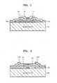
- FIG. 1is a schematic cross-sectional view of a semiconductor device according to example embodiments.
- a patterned active layer 11 including an amorphous ZnO based composite semiconductormay be formed on a substrate 10 , and source and drain electrodes 12 s and 12 d may be formed on ends of the patterned active layer as illustrated in FIG. 1 .
- the source and drain electrodes 12 s and 12 dmay overlap with the ends of the patterned active layer 11 in a predetermined or given width, and may be insulated from a gate electrode 14 .
- the active layer 11may include an amorphous ZnO based composite material represented by Formula 1 below.
- x(Ga 2 O 3 ) ⁇ y(In 2 O 3 ) ⁇ z(ZnO) Formula 1wherein, about 0.75 ⁇ x/z ⁇ about 3.15, and about 0.55 ⁇ y/z ⁇ about 1.70.
- the Ioff currentwhen the amount of Ga is too low, the Ioff current may increase when exposed to light due to its light-sensitive characteristics. On the other hand, when the amount of Ga is too high, an Ion/Ioff ratio may decrease, resulting in the deterioration of TFT characteristics. When the amount of Ion current is too low, mobility of a carrier may decrease. On the other hand, when the amount of In current is too high, threshold voltage may vary due to its light-sensitive characteristics.
- x, y and zmay be about 0.75 ⁇ x/z ⁇ about 3.15, and about 0.55 ⁇ y/z ⁇ about 1.70, for example, about 0.85 ⁇ x/z ⁇ about 3.05, and about 0.65 ⁇ y/z ⁇ about 1.70, or about 1.15 ⁇ x/z ⁇ about 2.05, and 1.15 ⁇ y/z ⁇ 1.70, or about 1.25 ⁇ x/z ⁇ about 1.95, and about 1.25 ⁇ y/z ⁇ about 1.70, or about 1.25 ⁇ x/z ⁇ about 1.45, and about 1.45 ⁇ y/z ⁇ about 1.65.
- the amorphous ZnO based composite semiconductor material represented by Formula 1may be applied to a low temperature deposition, e.g., a plastic substrate and a soda lime glass.
- the amorphous propertymay provide uniformity for a display having relatively large areas.
- the amorphous ZnO based composite semiconductormay be formed using a composite target of a gallium (Ga) oxide, an indium (In) oxide, and a zinc (Zn) oxide by a conventional sputtering method, and also formed using chemical vapor deposition (CVD) and/or an atomic layer deposition (ALD).
- CVDchemical vapor deposition
- ALDatomic layer deposition
- the source and drain electrodes 12 s and 12 dmay be formed of a conductive metal oxide or a metal.
- the conductive metal oxidemay include commonly available tin-doped indium oxide (ITO), indium zinc oxide (IZO), and/or aluminum-doped zinc oxide (ZAO), and examples of the metal may include titanium (Ti), platinum (Pt), chromium (Cr), tungsten (W), aluminum (Al), nickel (Ni), copper (Cu), molybdenum (Mo), tantalum (Ta), and/or an alloy thereof.
- a metal layeris used as the source and drain electrodes, a plurality of metal layers may be formed.
- an n + layermay be formed between the metal layer and the active layer to improve contact characteristics, and the n + layer may be formed using a conductive metal oxide or an oxygen vacant Ga oxide-In oxide-Zn oxide composite.
- the substratemay be a silicon substrate, a glass substrate and/or a plastic substrate.
- a gate insulating layer 13may be formed on the active layer 11 and the source/drain electrodes 12 s and 12 d .
- a commonly available gate insulating materialmay be used to form the gate insulating layer 13 , for example, a high dielectric oxide (e.g., a silicon nitride, a silicon oxide, a hafnium oxide and/or an aluminum oxide), may be used.
- a gate electrode 14may be formed on the gate insulating layer 13 and may correspond to the active layer 11 .
- the gate electrode 14may be formed using the same metal used for a source/drain electrode layer 120 or other metals. For example, a metal of Ti, Pt, Cr, W, Al, Ni, Cu, Mo, or Ta, or an alloy thereof may be used. When the metal layer is used as the gate electrode, a plurality of metal layers may be formed. A metal oxide may also be used.
- the semiconductor devicemay have the structure illustrated in FIG. 2 by disposing the gate electrode in a different way from the structure illustrated in FIG. 1 .
- a gate electrode 21may be formed on a substrate 20
- a gate insulating layer 22may be formed on the gate electrode 21 .
- a patterned active layer 23 including an amorphous ZnO based composite semiconductormay be formed on the gate insulating layer 22 .
- Source and drain electrodes 24 s and 24 dmay be formed on ends of the patterned active layer 23 .
- Another example of a semiconductor devicemay also have a structure in which source/drain electrodes may be formed on a gate insulating layer and then an active layer may be formed on the source/drain electrodes, besides the stack structure illustrated in FIGS. 1 and 2 .
- FIGS. 3A-3Gare cross-sectional views illustrating a method of manufacturing the semiconductor device shown in FIG. 1 .
- a semiconductor material layer 11 ′may be formed on the substrate 10 to form the active layer 11 using a RF magnetron sputtering method, a DC magnetron sputtering method, a chemical vapor deposition (CVD) method and/or an atomic layer deposition (ALD) method.
- CVDchemical vapor deposition
- ALDatomic layer deposition
- the semiconductor material layer 11 ′may be patterned using a photolithographic method to obtain the active layer 11 .
- a source/drain material layer 12may be formed on the entire surface of the active layer 11 using a RF magnetron sputtering method, a CVD method, a vacuum evaporation method, an e-beam evaporation method and/or an ALD method.
- the source/drain material layer 12may be patterned to form the source and drain electrodes 12 s and 12 d contacting the ends of the active layer 11 .
- a material that is used to form the gate insulating layer 13may be deposited using a conventional method, e.g., chemical vapor deposition (CVD) method and/or a plasma enhanced chemical vapor deposition (PECVD) method, to form the gate insulating layer 13 covering the source and drain electrodes 12 s and 12 d on the entire surface of the resultant stack structure.
- CVDchemical vapor deposition
- PECVDplasma enhanced chemical vapor deposition
- a material for forming a gate electrodemay be deposited and patterned to form the gate electrode 14 facing the active layer 11 .
- the stack structure including the active layer 11 and the source and drain electrodes 12 s and 12 d contacting the ends of the active layer 11may be annealed at a temperature of about 400° C. or less.
- Annealingmay be performed using a general furnace, a rapid thermal annealing (RTA), a laser, or a hot plate in a nitrogen atmosphere.
- RTArapid thermal annealing
- Annealingmay stabilize a contact between the active layer 11 and the source/drain electrodes 12 s and 12 d.
- FIGS. 4A-4Eare cross-sectional views illustrating a method of manufacturing the semiconductor device shown in FIG. 2 .
- a material for forming the gate electrode 21may be deposited on the substrate 20 and patterned to form the gate electrode 21 .
- the gate insulating layer 22may be formed on the gate electrode 21 .
- the gate insulating layer 22may be formed using CVD or PECVD.
- a semiconductor film formed using a target that for forming an amorphous ZnO based composite semiconductor represented by Formula 1 abovemay be patterned to obtain the active layer 23 using a photolithographic method.
- a source/drain electrode materialmay be deposited and patterned to obtain the source and drain electrodes 24 s and 24 d.
- the stack structure including the active layer 23 and the source and drain electrodes 24 s and 24 d contacting the ends of the active layer 23may be annealed.
- Annealingmay be performed at a temperature of about 450° C. or less, for example, about 200° C. to about 350° C., in an inert gas atmosphere, e.g., a nitrogen atmosphere.
- the annealingmay be performed using a general furnace, a RTA, a laser, or a hot plate. Annealing may stabilize a contact between the active layer 23 and the source/drain electrodes 24 s and 24 d.
- a semiconductor filmmay be formed using a composite oxide target of gallium (Ga), indium (In), and zinc (Zn) in an atomic ratio of about 1:1:1, about 2:2:1, about 3:2:1 and about 4:2:1 by using molybdenum (Mo) as a gate electrode material after forming a silicon nitride layer using a gate insulating material.
- Momolybdenum
- the semiconductor filmmay be patterned to form an active layer.
- IZOmay be deposited and patterned to form source/drain electrodes, the resultant may be annealed in a nitrogen atmosphere and a passivation layer may be formed of a silicon oxide.
- ICPinductively coupled plasma
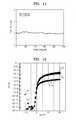
- a constant current testwas performed using a TFT having a Ga:In:Zn ratio of about 2.7:3.1:1.0, and the results are shown in FIG. 11 .
- the constant current testmay be performed at a temperature of about 45° C. for about 100 hours and a current applied to the source-drain electrodes may be about 3 ⁇ A.
- a voltage variation (Delta V) between the source and drain electrodesremained at about 0.3 V or less.
- variations in a gate voltage (Vg) and a drain current (Id) before and after a constant current testwere measured, and the results are illustrated in FIGS. 12 and 13 .
- FIG. 12is a graph illustrating results measured before a constant current test.
- An on-currentmay be about 10 ⁇ 4 A, and an off-current may be about 10 ⁇ 12 A, and thus the ratio of the on-current to the off current may be about 10 8 .
- Mobility on the active layermay be about 40 cm 2 /Vs, and a gate swing voltage may be about 0.385 V/dec.
- FIG. 13is a graph illustrating results measured after a constant current test. Upon comparing FIGS. 12 and 13 , the constant current test results may not differ greatly from each other. In other words, the ZnO based TFT may maintain its original electrical characteristics even after a constant current test in which about 3 ⁇ A may be applied for 100 hours.
- an electrically stable TFTmay be obtained by using an active layer including an amorphous ZnO based composite semiconductor due to improved optical sensitivity.
- the amorphous property of the ZnO based composite semiconductormay provide improved uniformity, and thus may be applied to display devices having relatively large areas.
Landscapes
- Thin Film Transistor (AREA)
Abstract
Description
- This non-provisional application claims priority under 35 U.S.C. § 119 to Korean Patent Application Nos. 10-2006-0034675, filed on Apr. 17, 2006, 10-2006-0043943, filed on May 16, 2006, and 10-2007-0029380, filed on Mar. 26, 2007 in the Korean Intellectual Property Office (KIPO), the entire contents of which are incorporated herein by reference.
- 1. Field
- Example embodiments relate to a semiconductor device and methods of manufacturing the same. Other example embodiments relate to a ZnO based thin film transistor including an active layer using a composite semiconductor material in which a zinc (Zn) oxide is doped with gallium (Ga) and indium (In) and methods of manufacturing the same.
- 2. Description of the Related Art
- Research on organic light-emitting diodes (OLED) having a relatively large area has been actively conducted. As a driving transistor for OLEDs, a transistor that stably operates with constant current characteristics and has improved durability needs to be developed. Amorphous silicon TFTs may be manufactured using a low temperature process, but such TFTs may have relatively low mobility and may not satisfy constant current bias conditions. On the other hand, polycrystalline silicon TFTs may have increased mobility and may satisfy constant current test conditions, but may not have uniform characteristics. Thus, polycrystalline silicon TFTs may not have relatively large areas and may require high temperature processes.
- ZnO materials may have conductivity, semiconductivity, and resistance according to their oxygen content. A transistor including a ZnO based semiconductor material as an active layer has been reported. In order to apply the transistor including a ZnO based semiconductor material as an active layer to display devices including OLEDs and LCDs, stable driving characteristics, which present constant characteristics in an on or off state, may be required in addition to constant current characteristics.
- Example embodiments provide an amorphous ZnO based thin film transistor having constant driving characteristics in an on or off state due to improved optical sensitivity, and methods of manufacturing the same.
- According to example embodiments, a semiconductor device may include a substrate, an active layer including a composite represented by Formula 1 below, on the substrate, source and drain electrodes electrically connected to the active layer, a gate electrode on the active layer, and a gate insulating layer between the gate electrode and the active layer:
x(Ga2O3)·y(In2O3)·z(ZnO)Formula 1
wherein, about 0.75≦x/z≦about 3.15, and about 0.55≦y/z≦about 1.70. - According to example embodiments, x, y, and z may be about 0.85≦x/z≦about 3.05, and about 0.65≦y/z≦about 1.70 in Formula 1. According to example embodiments, x, y, and z may be about 1.15≦x/z≦about 2.05, and about 1.15≦y/z≦about 1.70 in Formula 1. According to example embodiments, x, y, and z may be about 1.25≦x/z≦about 1.95, and about 1.25≦y/z≦about 1.70 in Formula 1. According to example embodiments, x, y, and z may be about 1.25≦x/z≦about 1.45, and about 1.45≦y/z≦about 1.65 in Formula 1.
- According to example embodiments, a method of manufacturing a semiconductor device may include forming an active layer including a composite represented by Formula 1 below, source and drain electrodes, a gate insulating layer and a gate electrode on a substrate,
x(Ga2O3)·y(In2O3)·z(ZnO)Formula 1
wherein, about 0.75≦x/z≦about 3.15, and about 0.55≦y/z≦about 1.70. - According to example embodiments, the active layer may be formed on the substrate, the source and drain electrodes may be formed to be electrically connected to the active layer, the gate insulating layer may be formed on the active layer, and the gate electrode may be formed on the active layer. On the other hand, the gate electrode may be formed on the substrate, the gate insulating layer may be formed on the gate electrode, the active layer may be formed on the gate insulating layer, and the source and drain electrodes may be formed to be electrically connected to the active layer.
- Example embodiments will be more clearly understood from the following detailed description taken in conjunction with the accompanying drawings.
FIGS. 1-5 represent non-limiting, example embodiments as described herein. FIG. 1 is a schematic cross-sectional view of a semiconductor device according to example embodiments;FIG. 2 is a schematic cross-sectional view of a semiconductor device according to example embodiments;FIGS. 3A-3G are cross-sectional views illustrating a method of manufacturing the example embodiment shown inFIG. 1 ;FIGS. 4A-4E are cross-sectional views illustrating a method of manufacturing another example embodiment shown inFIG. 2 ;FIG. 5 is a graph illustrating results of an inductively coupled plasma (ICP) analysis of ZnO based TFTs;FIGS. 6-10 are graphs illustrating results of an optical sensitivity analysis of ZnO based TFTs, and variations in a gate voltage (Vg) and a drain current (Id);FIG. 11 is a graph illustrating results of a constant current test of a ZnO based TFT; andFIGS. 12 and 13 are graphs illustrating variations in a gate voltage (Vg) and a drain current (Id) of the ZnO based TFT before and after the constant current test.- It should be noted that these Figures are intended to illustrate the general characteristics of methods, structure and/or materials utilized in certain example embodiments and to supplement the written description provided below. These drawings are not, however, to scale and may not precisely reflect the precise structural or performance characteristics of any given embodiment, and should not be interpreted as defining or limiting the range of values or properties encompassed by example embodiments. For example, the relative thicknesses and positioning of molecules, layers, regions and/or structural elements may be reduced or exaggerated for clarity. The use of similar or identical reference numbers in the various drawings is intended to indicate the presence of a similar or identical element or feature.
- Hereinafter, example embodiments will now be described more fully with reference to the accompanying drawings, in which example embodiments are shown. Example embodiments may, however, be embodied in many different forms and should not be construed as being limited to the embodiments set forth herein; rather, these embodiments are provided so that this disclosure will be thorough and complete, and will fully convey the concept of example embodiments to those skilled in the art.
- It will be understood that when an element or layer is referred to as being “on”, “connected to” or “coupled to” another element or layer, it can be directly on, connected or coupled to the other element or layer or intervening elements or layers may be present. In contrast, when an element is referred to as being “directly on,” “directly connected to” or “directly coupled to” another element or layer, there are no intervening elements or layers present. Like numbers refer to like elements throughout. As used herein, the term “and/or” includes any and all combinations of one or more of the associated listed items.
- It will be understood that, although the terms first, second, third etc. may be used herein to describe various elements, components, regions, layers and/or sections, these elements, components, regions, layers and/or sections should not be limited by these terms. These terms are only used to distinguish one element, component, region, layer or section from another region, layer or section. Thus, a first element, component, region, layer or section discussed below could be termed a second element, component, region, layer or section without departing from the teachings of example embodiments.
- Spatially relative terms, such as “beneath,” “below,” “lower,” “above,” “upper” and the like, may be used herein for ease of description to describe one element or feature's relationship to another element(s) or feature(s) as illustrated in the figures. It will be understood that the spatially relative terms are intended to encompass different orientations of the device in use or operation in addition to the orientation depicted in the figures. For example, if the device in the figures is turned over, elements described as “below” or “beneath” other elements or features would then be oriented “above” the other elements or features. Thus, the exemplary term “below” can encompass both an orientation of above and below. The device may be otherwise oriented (rotated 90 degrees or at other orientations) and the spatially relative descriptors used herein interpreted accordingly.
- The terminology used herein is for the purpose of describing particular embodiments only and is not intended to be limiting of example embodiments. As used herein, the singular forms “a,” “an” and “the” are intended to include the plural forms as well, unless the context clearly indicates otherwise. It will be further understood that the terms “comprises” and/or “comprising,” when used in this specification, specify the presence of stated features, integers, steps, operations, elements, and/or components, but do not preclude the presence or addition of one or more other features, integers, steps, operations, elements, components, and/or groups thereof.
- Example embodiments are described herein with reference to cross-sectional illustrations that are schematic illustrations of idealized embodiments (and intermediate structures) of example embodiments. As such, variations from the shapes of the illustrations as a result, for example, of manufacturing techniques and/or tolerances, are to be expected. Thus, example embodiments should not be construed as limited to the particular shapes of regions illustrated herein but are to include deviations in shapes that result, for example, from manufacturing. For example, an implanted region illustrated as a rectangle will, typically, have rounded or curved features and/or a gradient of implant concentration at its edges rather than a binary change from implanted to non-implanted region. Likewise, a buried region formed by implantation may result in some implantation in the region between the buried region and the surface through which the implantation takes place. Thus, the regions illustrated in the figures are schematic in nature and their shapes are not intended to illustrate the actual shape of a region of a device and are not intended to limit the scope of example embodiments.
- Unless otherwise defined, all terms (including technical and scientific terms) used herein have the same meaning as commonly understood by one of ordinary skill in the art to which example embodiments belong. It will be further understood that terms, such as those defined in commonly used dictionaries, should be interpreted as having a meaning that is consistent with their meaning in the context of the relevant art and will not be interpreted in an idealized or overly formal sense unless expressly so defined herein.
FIG. 1 is a schematic cross-sectional view of a semiconductor device according to example embodiments. Referring toFIG. 1 , a patternedactive layer 11 including an amorphous ZnO based composite semiconductor may be formed on asubstrate 10, and source and drainelectrodes FIG. 1 . The source and drainelectrodes active layer 11 in a predetermined or given width, and may be insulated from agate electrode 14.- The
active layer 11 may include an amorphous ZnO based composite material represented byFormula 1 below.
x(Ga2O3)·y(In2O3)·z(ZnO)Formula 1
wherein, about 0.75≦x/z≦about 3.15, and about 0.55≦y/z≦about 1.70. - In the amorphous ZnO based composite semiconductor, when the amount of Ga is too low, the Ioff current may increase when exposed to light due to its light-sensitive characteristics. On the other hand, when the amount of Ga is too high, an Ion/Ioff ratio may decrease, resulting in the deterioration of TFT characteristics. When the amount of Ion current is too low, mobility of a carrier may decrease. On the other hand, when the amount of In current is too high, threshold voltage may vary due to its light-sensitive characteristics.
- In the above formula, x, y and z may be about 0.75≦x/z≦about 3.15, and about 0.55≦y/z≦about 1.70, for example, about 0.85≦x/z≦about 3.05, and about 0.65≦y/z≦about 1.70, or about 1.15≦x/z≦about 2.05, and 1.15≦y/z≦1.70, or about 1.25≦x/z≦about 1.95, and about 1.25≦y/z≦about 1.70, or about 1.25≦x/z≦about 1.45, and about 1.45≦y/z≦about 1.65.
- The amorphous ZnO based composite semiconductor material represented by
Formula 1 may be applied to a low temperature deposition, e.g., a plastic substrate and a soda lime glass. The amorphous property may provide uniformity for a display having relatively large areas. The amorphous ZnO based composite semiconductor may be formed using a composite target of a gallium (Ga) oxide, an indium (In) oxide, and a zinc (Zn) oxide by a conventional sputtering method, and also formed using chemical vapor deposition (CVD) and/or an atomic layer deposition (ALD). - The source and drain
electrodes - A
gate insulating layer 13 may be formed on theactive layer 11 and the source/drain electrodes gate insulating layer 13, for example, a high dielectric oxide (e.g., a silicon nitride, a silicon oxide, a hafnium oxide and/or an aluminum oxide), may be used. - A
gate electrode 14 may be formed on thegate insulating layer 13 and may correspond to theactive layer 11. Thegate electrode 14 may be formed using the same metal used for a source/drain electrode layer120 or other metals. For example, a metal of Ti, Pt, Cr, W, Al, Ni, Cu, Mo, or Ta, or an alloy thereof may be used. When the metal layer is used as the gate electrode, a plurality of metal layers may be formed. A metal oxide may also be used. - The semiconductor device may have the structure illustrated in
FIG. 2 by disposing the gate electrode in a different way from the structure illustrated inFIG. 1 . Referring toFIG. 2 , agate electrode 21 may be formed on asubstrate 20, and agate insulating layer 22 may be formed on thegate electrode 21. A patternedactive layer 23 including an amorphous ZnO based composite semiconductor may be formed on thegate insulating layer 22. Source anddrain electrodes active layer 23. - Another example of a semiconductor device according to example embodiments may also have a structure in which source/drain electrodes may be formed on a gate insulating layer and then an active layer may be formed on the source/drain electrodes, besides the stack structure illustrated in
FIGS. 1 and 2 . - A method of manufacturing a semiconductor device according to example embodiments will now be described in detail.
FIGS. 3A-3G are cross-sectional views illustrating a method of manufacturing the semiconductor device shown inFIG. 1 . As shown inFIG. 3A , asemiconductor material layer 11′ may be formed on thesubstrate 10 to form theactive layer 11 using a RF magnetron sputtering method, a DC magnetron sputtering method, a chemical vapor deposition (CVD) method and/or an atomic layer deposition (ALD) method. - As shown in
FIG. 3B , thesemiconductor material layer 11′ may be patterned using a photolithographic method to obtain theactive layer 11. As shown inFIG. 3C , a source/drain material layer 12 may be formed on the entire surface of theactive layer 11 using a RF magnetron sputtering method, a CVD method, a vacuum evaporation method, an e-beam evaporation method and/or an ALD method. - As shown in
FIG. 3D , the source/drain material layer 12 may be patterned to form the source and drainelectrodes active layer 11. As shown inFIG. 3E , a material that is used to form thegate insulating layer 13 may be deposited using a conventional method, e.g., chemical vapor deposition (CVD) method and/or a plasma enhanced chemical vapor deposition (PECVD) method, to form thegate insulating layer 13 covering the source and drainelectrodes FIG. 3F , a material for forming a gate electrode may be deposited and patterned to form thegate electrode 14 facing theactive layer 11. - As shown in
FIG. 3G , the stack structure including theactive layer 11 and the source and drainelectrodes active layer 11 may be annealed at a temperature of about 400° C. or less. Annealing may be performed using a general furnace, a rapid thermal annealing (RTA), a laser, or a hot plate in a nitrogen atmosphere. Annealing may stabilize a contact between theactive layer 11 and the source/drain electrodes FIGS. 4A-4E are cross-sectional views illustrating a method of manufacturing the semiconductor device shown inFIG. 2 . As shown inFIG. 4A , a material for forming thegate electrode 21 may be deposited on thesubstrate 20 and patterned to form thegate electrode 21. As shown inFIG. 4B , thegate insulating layer 22 may be formed on thegate electrode 21. Thegate insulating layer 22 may be formed using CVD or PECVD. As shown inFIG. 4C , a semiconductor film formed using a target that for forming an amorphous ZnO based composite semiconductor represented byFormula 1 above may be patterned to obtain theactive layer 23 using a photolithographic method. As shown inFIG. 4D , a source/drain electrode material may be deposited and patterned to obtain the source and drainelectrodes - As shown in
FIG. 4E , the stack structure including theactive layer 23 and the source and drainelectrodes active layer 23 may be annealed. Annealing may be performed at a temperature of about 450° C. or less, for example, about 200° C. to about 350° C., in an inert gas atmosphere, e.g., a nitrogen atmosphere. The annealing may be performed using a general furnace, a RTA, a laser, or a hot plate. Annealing may stabilize a contact between theactive layer 23 and the source/drain electrodes - A semiconductor film may be formed using a composite oxide target of gallium (Ga), indium (In), and zinc (Zn) in an atomic ratio of about 1:1:1, about 2:2:1, about 3:2:1 and about 4:2:1 by using molybdenum (Mo) as a gate electrode material after forming a silicon nitride layer using a gate insulating material. The semiconductor film may be patterned to form an active layer. IZO may be deposited and patterned to form source/drain electrodes, the resultant may be annealed in a nitrogen atmosphere and a passivation layer may be formed of a silicon oxide.
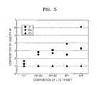
- An inductively coupled plasma (ICP) analysis on the semiconductor film formed according to the processes described above may be performed to measure the ratio of gallium (Ga), indium (In) and zinc (Zn), and the results are shown in Table 1 below and
FIG. 5 . Variations in a gate voltage (Vg) and a drain current (Id), when both light is on and off, are measured, and the results are shown inFIGS. 6-10 .TABLE 1 Ga, In, Zn atomic ratio in 1:1:1 2:2:1 2:2:1 3:2:1 4:2:1 the target Ga:In:Zn atom ratio in 1.7:1.3:1.0 2.5:2.8:1.0 2.7:3.1:1.0 3.9:2.5:1.0 6.1:3.2:1.0 active layer (ICP analysis) x/z 0.85 1.25 1.35 1.95 3.05 y/z 0.65 1.4 1.55 1.25 1.60 optical sensitivity analysis results
※ error range of ±0.2 in ICP analysis - A constant current test was performed using a TFT having a Ga:In:Zn ratio of about 2.7:3.1:1.0, and the results are shown in
FIG. 11 . The constant current test may be performed at a temperature of about 45° C. for about 100 hours and a current applied to the source-drain electrodes may be about 3 μA. As illustrated inFIG. 11 , a voltage variation (Delta V) between the source and drain electrodes remained at about 0.3 V or less. In addition, variations in a gate voltage (Vg) and a drain current (Id) before and after a constant current test were measured, and the results are illustrated inFIGS. 12 and 13 . FIG. 12 is a graph illustrating results measured before a constant current test. An on-current may be about 10−4A, and an off-current may be about 10−12A, and thus the ratio of the on-current to the off current may be about 108. Mobility on the active layer may be about 40 cm2/Vs, and a gate swing voltage may be about 0.385 V/dec.FIG. 13 is a graph illustrating results measured after a constant current test. Upon comparingFIGS. 12 and 13 , the constant current test results may not differ greatly from each other. In other words, the ZnO based TFT may maintain its original electrical characteristics even after a constant current test in which about 3 μA may be applied for 100 hours.- According to example embodiments, an electrically stable TFT may be obtained by using an active layer including an amorphous ZnO based composite semiconductor due to improved optical sensitivity. The amorphous property of the ZnO based composite semiconductor may provide improved uniformity, and thus may be applied to display devices having relatively large areas.
- Various electronic devices and apparatuses using the ZnO based TFT according to example embodiments may be manufactured by those of ordinary skill in the art according to example embodiments. While example embodiments have been particularly shown and described with reference to example embodiments thereof, it will be understood by those of ordinary skill in the art that various changes in form and details may be made therein without departing from the spirit and scope of the following claims.
Claims (23)
1. A semiconductor device comprising:
x(Ga2O3)·y(In2O3)·z(ZnO) Formula 1
a substrate;
an active layer including a composite represented by Formula 1 below, on the substrate;
source and drain electrodes electrically connected to the active layer;
a gate electrode on the active layer; and
a gate insulating layer between the gate electrode and the active layer:
x(Ga2O3)·y(In2O3)·z(ZnO) Formula 1
wherein, about 0.75≦x/z≦about 3.15, and about 0.55≦y/z≦about 1.70.
2. The semiconductor device ofclaim 1 , wherein x, y, and z are about 0.85≦x/z≦about 3.05, and about 0.65≦y/z≦about 1.70 in Formula 1.
3. The semiconductor device ofclaim 1 , wherein x, y, and z are about 1.15≦x/z≦about 2.05, and about 1.15≦y/z≦about 1.70 in Formula 1.
4. The semiconductor device ofclaim 1 , wherein x, y, and z are about 1.25≦x/z≦about 1.95, and about 1.25≦y/z≦about 1.70 in Formula 1.
5. The semiconductor device ofclaim 1 , wherein x, y, and z are about 1.25≦x/z≦about 1.45, and about 1.45≦y/z≦about 1.65 in Formula 1.
6. The semiconductor device ofclaim 1 , wherein the source and drain electrodes are formed of a metal oxide selected from the group consisting of tin-doped indium oxide (ITO), indium zinc oxide (IZO), and aluminum-doped zinc oxide (ZAO).
7. The semiconductor device ofclaim 1 , wherein the source and drain electrodes include a metal selected from the group consisting of titanium (Ti), platinum (Pt), chromium (Cr), tungsten (W), aluminum (Al), nickel (Ni), copper (Cu), molybdenum (Mo), tantalum (Ta) and an alloy thereof.
8. The semiconductor device ofclaim 7 , wherein the source and drain electrodes are formed of a plurality of metal layers.
9. The semiconductor device ofclaim 7 , wherein an n+ layer is formed between the source or drain electrode and the active layer.
10. The semiconductor device ofclaim 1 , wherein the gate insulating layer includes a nitride, an oxide, or a high dielectric oxide.
11. The semiconductor device ofclaim 1 , wherein the gate electrode includes a metal selected from the group consisting of titanium (Ti), platinum (Pt), chromium (Cr), tungsten (W), aluminum (Al), nickel (Ni), copper (Cu), molybdenum (Mo), tantalum (Ta) and an alloy thereof.
12. The semiconductor device ofclaim 1 , wherein the substrate is a glass substrate or a plastic substrate.
13. A method of manufacturing a semiconductor device, the method comprising:
x(Ga2O3)·y(In2O3)·z(ZnO) Formula 1
forming an active layer including a composite represented by Formula 1 below, source and drain electrodes, a gate insulating layer and a gate electrode on a substrate,
x(Ga2O3)·y(In2O3)·z(ZnO) Formula 1
wherein, about 0.75≦x/z≦about 3.15, and about 0.55≦y/z≦about 1.70.
14. The method ofclaim 13 , wherein the active layer is formed on the substrate, the source and drain electrodes are formed to be electrically connected to the active layer, the gate insulating layer is formed on the active layer, and the gate electrode is formed on the active layer.
15. The method ofclaim 13 , wherein the gate electrode is formed on the substrate, the gate insulating layer is formed on the gate electrode, the active layer is formed on the gate insulating layer, and the source and drain electrodes are formed to be electrically connected to the active layer.
16. The method ofclaim 13 , wherein x, y and z are about 0.85≦x/z≦about 3.05, and about 0.65≦y/z≦about 1.70 in Formula 1.
17. The method ofclaim 13 , wherein x, y, and z are about 1.15≦x/z≦about 2.05, and about 1.15≦y/z≦about 1.70 in Formula 1.
18. The method ofclaim 13 , wherein x, y, and z are about 1.25≦x/z≦about 1.95, and about 1.25≦y/z≦about 1.70 in Formula 1.
19. The method ofclaim 13 , wherein x, y, and z are about 1.25≦x/z≦about 1.45, and about 1.45≦y/z≦about 1.65 in Formula 1.
20. The method ofclaim 13 , wherein the source and drain electrodes are formed of a metal oxide.
21. The method ofclaim 13 , further comprising:
forming an n+ layer between the active layer and the source and drain electrodes.
22. The method ofclaim 13 , further comprising:
annealing the active layer and the source and drain electrodes, after forming the active layer and the source and drain electrodes.
23. The method ofclaim 22 , wherein annealing is performed at a temperature of about 400° C. or less in a nitrogen atmosphere.
Priority Applications (2)
| Application Number | Priority Date | Filing Date | Title |
|---|---|---|---|
| US12/929,323US8735882B2 (en) | 2006-04-17 | 2011-01-14 | ZnO based semiconductor devices and methods of manufacturing the same |
| US12/929,324US8421070B2 (en) | 2006-04-17 | 2011-01-14 | ZnO based semiconductor devices and methods of manufacturing the same |
Applications Claiming Priority (6)
| Application Number | Priority Date | Filing Date | Title |
|---|---|---|---|
| KR20060034675 | 2006-04-17 | ||
| KR10-2006-0034675 | 2006-04-17 | ||
| KR10-2006-0043943 | 2006-05-16 | ||
| KR20060043943 | 2006-05-16 | ||
| KR1020070029380AKR100785038B1 (en) | 2006-04-17 | 2007-03-26 | Amorphous ZnO based Thin Film Transistor |
| KR10-2007-0029380 | 2007-03-26 |
Related Child Applications (2)
| Application Number | Title | Priority Date | Filing Date |
|---|---|---|---|
| US12/929,324ContinuationUS8421070B2 (en) | 2006-04-17 | 2011-01-14 | ZnO based semiconductor devices and methods of manufacturing the same |
| US12/929,323ContinuationUS8735882B2 (en) | 2006-04-17 | 2011-01-14 | ZnO based semiconductor devices and methods of manufacturing the same |
Publications (2)
| Publication Number | Publication Date |
|---|---|
| US20070252147A1true US20070252147A1 (en) | 2007-11-01 |
| US7893431B2 US7893431B2 (en) | 2011-02-22 |
Family
ID=38817614
Family Applications (3)
| Application Number | Title | Priority Date | Filing Date |
|---|---|---|---|
| US11/785,269Active2028-12-02US7893431B2 (en) | 2006-04-17 | 2007-04-17 | ZnO based semiconductor devices and methods of manufacturing the same |
| US12/929,324ActiveUS8421070B2 (en) | 2006-04-17 | 2011-01-14 | ZnO based semiconductor devices and methods of manufacturing the same |
| US12/929,323Active2027-05-04US8735882B2 (en) | 2006-04-17 | 2011-01-14 | ZnO based semiconductor devices and methods of manufacturing the same |
Family Applications After (2)
| Application Number | Title | Priority Date | Filing Date |
|---|---|---|---|
| US12/929,324ActiveUS8421070B2 (en) | 2006-04-17 | 2011-01-14 | ZnO based semiconductor devices and methods of manufacturing the same |
| US12/929,323Active2027-05-04US8735882B2 (en) | 2006-04-17 | 2011-01-14 | ZnO based semiconductor devices and methods of manufacturing the same |
Country Status (6)
| Country | Link |
|---|---|
| US (3) | US7893431B2 (en) |
| EP (1) | EP2008310B1 (en) |
| JP (1) | JP5137146B2 (en) |
| KR (2) | KR100785038B1 (en) |
| CN (1) | CN101473444B (en) |
| WO (1) | WO2007120010A1 (en) |
Cited By (32)
| Publication number | Priority date | Publication date | Assignee | Title |
|---|---|---|---|---|
| US20090050884A1 (en)* | 2007-08-02 | 2009-02-26 | Yan Ye | Thin film transistors using thin film semiconductor materials |
| US20090230390A1 (en)* | 2008-03-13 | 2009-09-17 | Sony Corporation | Thin film transistor and display |
| US20090233424A1 (en)* | 2008-03-14 | 2009-09-17 | Yan Ye | Thin film metal oxynitride semiconductors |
| US20090250693A1 (en)* | 2008-04-03 | 2009-10-08 | Hong-Han Jeong | Thin film transistor, display device, including the same, and associated methods |
| US20100001272A1 (en)* | 2008-07-02 | 2010-01-07 | Applied Materials, Inc. | Thin film transistors using multiple active channel layers |
| US20100044701A1 (en)* | 2007-02-20 | 2010-02-25 | Canon Kabushiki Kaisha | Thin-film transistor fabrication process and display device |
| US20100102312A1 (en)* | 2008-10-24 | 2010-04-29 | Shunpei Yamazaki | Oxide semiconductor, thin film transistor, and display device |
| US20100102311A1 (en)* | 2008-10-24 | 2010-04-29 | Semiconductor Energy Laboratory Co., Ltd. | Oxide semiconductor, thin film transistor, and display device |
| US20100176392A1 (en)* | 2009-01-12 | 2010-07-15 | Ki-Nyeng Kang | Thin film transistor and method of manufacturing the same |
| US20100304528A1 (en)* | 2009-06-02 | 2010-12-02 | Kim Dae-Won | Method of fabricating oxide thin film transistor |
| US20100321279A1 (en)* | 2009-06-17 | 2010-12-23 | Samsung Electronics Co., Ltd. | Transistor, electronic device including a transistor and methods of manufacturing the same |
| US20110042668A1 (en)* | 2009-08-18 | 2011-02-24 | Fujifilm Corporation | Amorphous oxide semiconductor material, field-effect transistor, and display device |
| JP2011119718A (en)* | 2009-11-06 | 2011-06-16 | Semiconductor Energy Lab Co Ltd | Semiconductor device and method of manufacturing the same |
| US7988470B2 (en) | 2009-09-24 | 2011-08-02 | Applied Materials, Inc. | Methods of fabricating metal oxide or metal oxynitride TFTs using wet process for source-drain metal etch |
| US20110261017A1 (en)* | 2010-04-22 | 2011-10-27 | Samsung Electronics Co., Ltd. | Light sensing circuit, and remote optical touch panel and image acquisition apparatus including the light sensing circuit |
| US20110284722A1 (en)* | 2010-05-20 | 2011-11-24 | Samsung Electronics Co., Ltd. | Light-sensing circuit, method of operating the light-sensing circuit, and light-sensing apparatus employing the light-sensing circuit |
| US8143093B2 (en) | 2008-03-20 | 2012-03-27 | Applied Materials, Inc. | Process to make metal oxide thin film transistor array with etch stopping layer |
| US20120274608A1 (en)* | 2010-04-22 | 2012-11-01 | Samsung Electronics Co., Ltd. | Simplified light sensing circuit, light sensing apparatus including the light sensing circuit, method of driving the light sensing apparatus, and image acquisition apparatus and optical touch screen apparatus including the light sensing apparatus |
| US8784699B2 (en) | 2009-11-19 | 2014-07-22 | Idemitsu Kosan Co., Ltd. | In-Ga-Zn-type oxide, oxide sintered body, and sputtering target |
| US8829513B2 (en) | 2009-08-31 | 2014-09-09 | Sharp Kabushiki Kaisha | Oxide semiconductor including Ga, In, Zn, and O and A thin film transistor and a display with the oxide semiconductor including Ga, In, Zn, and O |
| US8840763B2 (en) | 2009-09-28 | 2014-09-23 | Applied Materials, Inc. | Methods for stable process in a reactive sputtering process using zinc or doped zinc target |
| TWI474407B (en)* | 2009-02-13 | 2015-02-21 | Ulvac Inc | A method for manufacturing a transistor, a transistor, and a sputtering target |
| US20150179112A1 (en)* | 2010-07-02 | 2015-06-25 | Semiconductor Energy Laboratory Co., Ltd. | Liquid crystal display device |
| JP2015128165A (en)* | 2008-10-03 | 2015-07-09 | 株式会社半導体エネルギー研究所 | Oxide semiconductor layer |
| US9443981B2 (en) | 2009-02-20 | 2016-09-13 | Semiconductor Energy Laboratory Co., Ltd. | Thin film transistor, method for manufacturing the same, and semiconductor device |
| JP2016167623A (en)* | 2008-07-31 | 2016-09-15 | 株式会社半導体エネルギー研究所 | Semiconductor device |
| US9698278B2 (en) | 2013-12-24 | 2017-07-04 | Boe Technology Group Co., Ltd. | Thin film transistor and manufacturing method thereof, array substrate, display device |
| JP2019041117A (en)* | 2009-12-04 | 2019-03-14 | 株式会社半導体エネルギー研究所 | Method for manufacturing semiconductor device |
| US11075303B2 (en)* | 2016-03-02 | 2021-07-27 | Tokyo Institute Of Technology | Oxide semiconductor compound, semiconductor element provided with layer of oxide semiconductor compound, and laminated body |
| US20210366709A1 (en)* | 2009-06-30 | 2021-11-25 | Semiconductor Energy Laboratory Co., Ltd. | Semiconductor device and method for manufacturing the same |
| US20220109009A1 (en)* | 2019-05-13 | 2022-04-07 | Hewlett-Packard Development Company, L.P. | Thin-film transistors |
| US11437411B2 (en)* | 2019-07-24 | 2022-09-06 | Shenzhen China Star Optoelectronics Semiconductor Display Technology Co., Ltd. | Thin film transistor drive backplane and micro-light emitting diode display |
Families Citing this family (59)
| Publication number | Priority date | Publication date | Assignee | Title |
|---|---|---|---|---|
| KR100785038B1 (en)* | 2006-04-17 | 2007-12-12 | 삼성전자주식회사 | Amorphous ZnO based Thin Film Transistor |
| JP2008277326A (en) | 2007-04-25 | 2008-11-13 | Canon Inc | Amorphous oxide semiconductor, semiconductor device and thin film transistor |
| KR101441542B1 (en) | 2008-03-26 | 2014-09-18 | 삼성디스플레이 주식회사 | Thin film transistor substrate, display device including same, and method of manufacturing thin film transistor substrate |
| KR100941855B1 (en)* | 2008-04-04 | 2010-02-12 | 삼성모바일디스플레이주식회사 | Thin film transistor, its manufacturing method, and flat panel display device comprising thin film transistor |
| CN102067281B (en) | 2008-04-25 | 2013-06-12 | 株式会社半导体能源研究所 | Semiconductor device and method for manufacturing the same |
| KR20090124527A (en) | 2008-05-30 | 2009-12-03 | 삼성모바일디스플레이주식회사 | Thin film transistor, its manufacturing method, and flat panel display device comprising thin film transistor |
| KR101487256B1 (en)* | 2008-07-22 | 2015-01-29 | 엘지디스플레이 주식회사 | Method of fabricating oxide thin film transistor |
| TWI491048B (en) | 2008-07-31 | 2015-07-01 | Semiconductor Energy Lab | Semiconductor device |
| TWI469354B (en) | 2008-07-31 | 2015-01-11 | Semiconductor Energy Lab | Semiconductor device and method of manufacturing same |
| TWI424506B (en)* | 2008-08-08 | 2014-01-21 | Semiconductor Energy Lab | Semiconductor device manufacturing method |
| JP5525778B2 (en)* | 2008-08-08 | 2014-06-18 | 株式会社半導体エネルギー研究所 | Semiconductor device |
| US9082857B2 (en)* | 2008-09-01 | 2015-07-14 | Semiconductor Energy Laboratory Co., Ltd. | Semiconductor device comprising an oxide semiconductor layer |
| JP5627071B2 (en) | 2008-09-01 | 2014-11-19 | 株式会社半導体エネルギー研究所 | Method for manufacturing semiconductor device |
| WO2010029865A1 (en)* | 2008-09-12 | 2010-03-18 | Semiconductor Energy Laboratory Co., Ltd. | Display device |
| CN102160184B (en)* | 2008-09-19 | 2014-07-09 | 株式会社半导体能源研究所 | Display device |
| KR101670695B1 (en) | 2008-09-19 | 2016-10-31 | 가부시키가이샤 한도오따이 에네루기 켄큐쇼 | Semiconductor device |
| JP5361651B2 (en)* | 2008-10-22 | 2013-12-04 | 株式会社半導体エネルギー研究所 | Method for manufacturing semiconductor device |
| EP2180518B1 (en)* | 2008-10-24 | 2018-04-25 | Semiconductor Energy Laboratory Co, Ltd. | Method for manufacturing semiconductor device |
| EP2184783B1 (en)* | 2008-11-07 | 2012-10-03 | Semiconductor Energy Laboratory Co, Ltd. | Semiconductor device and method for manufacturing the same |
| KR20170021903A (en)* | 2008-11-07 | 2017-02-28 | 가부시키가이샤 한도오따이 에네루기 켄큐쇼 | Method of manufacturing a semiconductor device |
| KR101592012B1 (en) | 2008-12-01 | 2016-02-05 | 삼성디스플레이 주식회사 | Organic light emitting device and manufacturing method thereof |
| KR101547326B1 (en) | 2008-12-04 | 2015-08-26 | 삼성전자주식회사 | Transistor and method of manufacturing the same |
| TWI501319B (en)* | 2008-12-26 | 2015-09-21 | Semiconductor Energy Lab | Semiconductor device and manufacturing method thereof |
| KR101594471B1 (en) | 2009-02-10 | 2016-02-29 | 삼성디스플레이 주식회사 | Thin film transistor substrate and manufacturing method thereof |
| US8378342B2 (en) | 2009-03-23 | 2013-02-19 | Samsung Electronics Co., Ltd. | Oxide semiconductor and thin film transistor including the same |
| EP2256795B1 (en) | 2009-05-29 | 2014-11-19 | Semiconductor Energy Laboratory Co., Ltd. | Manufacturing method for oxide semiconductor device |
| KR101810699B1 (en) | 2009-06-30 | 2018-01-25 | 가부시키가이샤 한도오따이 에네루기 켄큐쇼 | Method for manufacturing semiconductor device |
| WO2011001881A1 (en)* | 2009-06-30 | 2011-01-06 | Semiconductor Energy Laboratory Co., Ltd. | Method for manufacturing semiconductor device |
| KR102011616B1 (en) | 2009-06-30 | 2019-08-16 | 가부시키가이샤 한도오따이 에네루기 켄큐쇼 | Method for manufacturing semiconductor device |
| CN102511082B (en) | 2009-09-16 | 2016-04-27 | 株式会社半导体能源研究所 | Semiconductor device and manufacturing method thereof |
| KR102219095B1 (en)* | 2009-09-24 | 2021-02-23 | 가부시키가이샤 한도오따이 에네루기 켄큐쇼 | Semiconductor device and method for manufacturing the same |
| KR101767035B1 (en) | 2009-10-01 | 2017-08-10 | 가부시키가이샤 한도오따이 에네루기 켄큐쇼 | Semiconductor device and method for manufacturing the same |
| KR101745747B1 (en) | 2009-10-16 | 2017-06-27 | 가부시키가이샤 한도오따이 에네루기 켄큐쇼 | Logic circuit and semiconductor device |
| KR102393447B1 (en)* | 2009-11-13 | 2022-05-03 | 가부시키가이샤 한도오따이 에네루기 켄큐쇼 | Semiconductor device and manufacturing method thereof |
| JP4843083B2 (en)* | 2009-11-19 | 2011-12-21 | 出光興産株式会社 | In-Ga-Zn-based oxide sputtering target |
| KR101370301B1 (en) | 2009-11-20 | 2014-03-05 | 가부시키가이샤 한도오따이 에네루기 켄큐쇼 | Method for manufacturing semiconductor device |
| KR101631652B1 (en) | 2009-12-29 | 2016-06-20 | 삼성전자주식회사 | Image sensor using light-sensitive transparent oxide semiconductor material |
| JP5685107B2 (en)* | 2010-02-26 | 2015-03-18 | 株式会社半導体エネルギー研究所 | Method for manufacturing semiconductor device |
| JP5496745B2 (en)* | 2010-03-31 | 2014-05-21 | 富士フイルム株式会社 | Thin film field effect transistor and method of manufacturing the same |
| JP5548500B2 (en)* | 2010-03-31 | 2014-07-16 | 富士フイルム株式会社 | Method for manufacturing thin film field effect transistor |
| KR102056905B1 (en)* | 2011-07-25 | 2019-12-18 | 삼성전자주식회사 | Light sensing apparatus and method of driving the light sensing apparatus, and optical touch screen apparatus including the light sensing apparatus |
| KR20120000499A (en)* | 2010-06-25 | 2012-01-02 | 가부시키가이샤 한도오따이 에네루기 켄큐쇼 | Transistors and Semiconductor Devices |
| CN103500712B (en) | 2010-12-03 | 2016-05-25 | 株式会社半导体能源研究所 | Semiconductor device |
| JP5527225B2 (en)* | 2011-01-14 | 2014-06-18 | ソニー株式会社 | Thin film transistor and display device |
| TWI602303B (en)* | 2011-01-26 | 2017-10-11 | 半導體能源研究所股份有限公司 | Semiconductor device and method of manufacturing same |
| TWI582999B (en)* | 2011-03-25 | 2017-05-11 | 半導體能源研究所股份有限公司 | Field effect transistor and memory and semiconductor circuit including the field effect transistor |
| JP5800291B2 (en)* | 2011-04-13 | 2015-10-28 | ローム株式会社 | ZnO-based semiconductor device and manufacturing method thereof |
| KR20140003315A (en)* | 2011-06-08 | 2014-01-09 | 가부시키가이샤 한도오따이 에네루기 켄큐쇼 | Sputtering target, method for manufacturing sputtering target, and method for forming thin film |
| KR102282833B1 (en)* | 2011-06-17 | 2021-07-27 | 가부시키가이샤 한도오따이 에네루기 켄큐쇼 | Transistor |
| CN102296270B (en)* | 2011-08-30 | 2013-06-19 | 华南理工大学 | Doped zinc oxide semiconductor material, and preparation method and application thereof |
| US9048323B2 (en) | 2012-04-30 | 2015-06-02 | Semiconductor Energy Laboratory Co., Ltd. | Semiconductor device |
| KR20130137851A (en) | 2012-06-08 | 2013-12-18 | 삼성디스플레이 주식회사 | Precursor composition for oxide semiconductor, thin film transistor array panel including oxide semiconductor, and manufacturing method of thin film transistor array panel including oxide semiconductor |
| BR112015013198B1 (en) | 2012-12-07 | 2021-03-30 | Bemis Company, Inc | MULTILAYER FILM AND THERMOFORMED BLISTER PACKAGE OBTAINED FROM THIS FILM |
| JP2013093612A (en)* | 2013-01-22 | 2013-05-16 | Semiconductor Energy Lab Co Ltd | Oxide semiconductor and semiconductor device |
| JP2014060451A (en)* | 2013-12-18 | 2014-04-03 | Semiconductor Energy Lab Co Ltd | Light-emitting device |
| US20150225151A1 (en) | 2014-02-11 | 2015-08-13 | Christopher L. Osborn | Anti-Scalping Transdermal Patch Packaging Film |
| US9468584B2 (en) | 2014-04-02 | 2016-10-18 | Bemis Company, Inc. | Child-resistant packaging |
| KR102097692B1 (en)* | 2018-03-30 | 2020-05-26 | 호서대학교 산학협력단 | Thin film transistor and manufacturing method thereof |
| CN114582893A (en)* | 2022-03-10 | 2022-06-03 | 广州华星光电半导体显示技术有限公司 | Array substrate, manufacturing method of array substrate, and display device |
Citations (33)
| Publication number | Priority date | Publication date | Assignee | Title |
|---|---|---|---|---|
| US4960718A (en)* | 1985-12-13 | 1990-10-02 | Allied-Signal Inc. | MESFET device having a semiconductor surface barrier layer |
| US5656824A (en)* | 1995-06-02 | 1997-08-12 | Ois Optical Imaging Systems, Inc. | TFT with reduced channel length and method of making same |
| US5854139A (en)* | 1994-06-28 | 1998-12-29 | Hitachi, Ltd. | Organic field-effect transistor and production thereof |
| US5972527A (en)* | 1992-12-15 | 1999-10-26 | Idemitsu Kosan Co., Ltd. | Transparent electrically conductive layer, electrically conductive transparent substrate and electrically conductive material |
| US6107734A (en)* | 1998-05-20 | 2000-08-22 | Idemitsu Kosan Co., Ltd. | Organic EL light emitting element with light emitting layers and intermediate conductive layer |
| US20020074657A1 (en)* | 2000-10-11 | 2002-06-20 | Murata Manufacturing Co., Ltd. | Semiconductor ceramic having a negative temperature coefficient of resistance and negative temperature coefficient thermistor |
| US6563174B2 (en)* | 2001-09-10 | 2003-05-13 | Sharp Kabushiki Kaisha | Thin film transistor and matrix display device |
| US20030218221A1 (en)* | 2002-05-21 | 2003-11-27 | the State of Oregon acting by and through the behalf of Oregon State University | Transistor structures and methods for making the same |
| US6727522B1 (en)* | 1998-11-17 | 2004-04-27 | Japan Science And Technology Corporation | Transistor and semiconductor device |
| US20040180217A1 (en)* | 2001-08-02 | 2004-09-16 | Kazuyoshi Inoue | Sputtering target, transparent conductive film, and their manufacturing method |
| US20050062134A1 (en)* | 2003-09-18 | 2005-03-24 | Industrial Technology Research Institute | Compound semiconductor material and method for forming an active layer of a thin film transistor device |
| US6878962B1 (en)* | 1999-03-25 | 2005-04-12 | Japan Science And Technology Corp. | Semiconductor device |
| US20050199960A1 (en)* | 2004-03-12 | 2005-09-15 | Hoffman Randy L. | Semiconductor device |
| US20060003485A1 (en)* | 2004-06-30 | 2006-01-05 | Hoffman Randy L | Devices and methods of making the same |
| US20060068091A1 (en)* | 2004-09-30 | 2006-03-30 | Seiko Epson Corporation | Method for manufacturing functional film and method for manufacturing thin film transistor |
| US20060079034A1 (en)* | 2004-10-12 | 2006-04-13 | Randy Hoffman | Method to form a passivation layer |
| US20060091793A1 (en)* | 2004-11-02 | 2006-05-04 | 3M Innovative Properties Company | Methods and displays utilizing integrated zinc oxide row and column drivers in conjunction with organic light emitting diodes |
| US20060108529A1 (en)* | 2004-11-10 | 2006-05-25 | Canon Kabushiki Kaisha | Sensor and image pickup device |
| US20060108636A1 (en)* | 2004-11-10 | 2006-05-25 | Canon Kabushiki Kaisha | Amorphous oxide and field effect transistor |
| US20060110867A1 (en)* | 2004-11-10 | 2006-05-25 | Canon Kabushiki Kaisha | Field effect transistor manufacturing method |
| US20060113536A1 (en)* | 2004-11-10 | 2006-06-01 | Canon Kabushiki Kaisha | Display |
| US20060113539A1 (en)* | 2004-11-10 | 2006-06-01 | Canon Kabushiki Kaisha | Field effect transistor |
| US20060113549A1 (en)* | 2004-11-10 | 2006-06-01 | Canon Kabushiki Kaisha | Light-emitting device |
| US20060113565A1 (en)* | 2004-11-10 | 2006-06-01 | Canon Kabushiki Kaisha | Electric elements and circuits utilizing amorphous oxides |
| US7061014B2 (en)* | 2001-11-05 | 2006-06-13 | Japan Science And Technology Agency | Natural-superlattice homologous single crystal thin film, method for preparation thereof, and device using said single crystal thin film |
| US7067843B2 (en)* | 2002-10-11 | 2006-06-27 | E. I. Du Pont De Nemours And Company | Transparent oxide semiconductor thin film transistors |
| US20060244107A1 (en)* | 2003-06-20 | 2006-11-02 | Toshinori Sugihara | Semiconductor device, manufacturing method, and electronic device |
| US7145174B2 (en)* | 2004-03-12 | 2006-12-05 | Hewlett-Packard Development Company, Lp. | Semiconductor device |
| US20060284172A1 (en)* | 2005-06-10 | 2006-12-21 | Casio Computer Co., Ltd. | Thin film transistor having oxide semiconductor layer and manufacturing method thereof |
| US20060286737A1 (en)* | 2005-06-16 | 2006-12-21 | Levy David H | Methods of making thin film transistors comprising zinc-oxide-based semiconductor materials and transistors made thereby |
| US20060292777A1 (en)* | 2005-06-27 | 2006-12-28 | 3M Innovative Properties Company | Method for making electronic devices using metal oxide nanoparticles |
| US20070194379A1 (en)* | 2004-03-12 | 2007-08-23 | Japan Science And Technology Agency | Amorphous Oxide And Thin Film Transistor |
| US20070254399A1 (en)* | 2006-04-27 | 2007-11-01 | Industrial Technology Research Institute | Low temperature direct deposited polycrystalline silicon thin film transistor structure and method for manufacturing the same |
Family Cites Families (56)
| Publication number | Priority date | Publication date | Assignee | Title |
|---|---|---|---|---|
| JPH0244263B2 (en)* | 1987-04-22 | 1990-10-03 | Kagaku Gijutsucho Mukizaishitsu Kenkyushocho | INGAZN7O10DESHIMESARERUROTSUHOSHOKEINOSOJOKOZOOJUSURUKAGOBUTSUOYOBISONOSEIZOHO |
| JP3124101B2 (en) | 1992-01-30 | 2001-01-15 | ローム株式会社 | Nonvolatile semiconductor memory device and method of manufacturing the same |
| US5548132A (en) | 1994-10-24 | 1996-08-20 | Micron Technology, Inc. | Thin film transistor with large grain size DRW offset region and small grain size source and drain and channel regions |
| JPH10306367A (en)* | 1997-05-06 | 1998-11-17 | Sumitomo Metal Mining Co Ltd | ZnO-Ga2O3-based sintered body for sputtering target and method for producing the same |
| IL125604A (en)* | 1997-07-30 | 2004-03-28 | Saifun Semiconductors Ltd | Non-volatile electrically erasable and programmble semiconductor memory cell utilizing asymmetrical charge |
| US6338987B1 (en) | 1998-08-27 | 2002-01-15 | Lg.Philips Lcd Co., Ltd. | Method for forming polycrystalline silicon layer and method for fabricating thin film transistor |
| KR100317642B1 (en) | 1999-05-27 | 2001-12-22 | 구본준, 론 위라하디락사 | Method for manufacturing a Thin Film Transistor using a metal plating |
| US6998656B2 (en)* | 2003-02-07 | 2006-02-14 | Hewlett-Packard Development Company, L.P. | Transparent double-injection field-effect transistor |
| US6882012B2 (en)* | 2000-02-28 | 2005-04-19 | Semiconductor Energy Laboratory Co., Ltd. | Semiconductor device and a method of manufacturing the same |
| US6727533B2 (en) | 2000-11-29 | 2004-04-27 | Fujitsu Limited | Semiconductor apparatus having a large-size bus connection |
| JP2002320848A (en)* | 2001-02-23 | 2002-11-05 | Honda Motor Co Ltd | Hydrogen storage material |
| KR20020082637A (en)* | 2001-04-25 | 2002-10-31 | 광주과학기술원 | Metal electrode for light emitting diodes using n-ZnO group semiconductor and manufacturing method thereof |
| US20030014859A1 (en)* | 2001-07-23 | 2003-01-23 | Kejha Joseph B. | Method of automated hybrid lithium-ion cells production and method of the cell assembly and construction |
| TW546840B (en) | 2001-07-27 | 2003-08-11 | Hitachi Ltd | Non-volatile semiconductor memory device |
| US6562491B1 (en)* | 2001-10-15 | 2003-05-13 | Advanced Micro Devices, Inc. | Preparation of composite high-K dielectrics |
| CN1445821A (en)* | 2002-03-15 | 2003-10-01 | 三洋电机株式会社 | Forming method of ZnO film and ZnO semiconductor layer, semiconductor element and manufacturing method thereof |
| KR101023491B1 (en)* | 2002-05-21 | 2011-03-21 | 더 스테이트 오브 오레곤 액팅 바이 앤드 쓰루 더 스테이트 보드 오브 하이어 에쥬케이션 온 비해프 오브 오레곤 스테이트 유니버시티 | Transistor Structure and Manufacturing Method Thereof |
| US6929970B2 (en) | 2002-09-12 | 2005-08-16 | Agfa-Gevaert | Process for preparing nano-porous metal oxide semiconductor layers |
| US6858899B2 (en) | 2002-10-15 | 2005-02-22 | Matrix Semiconductor, Inc. | Thin film transistor with metal oxide layer and method of making same |
| EP1574596A1 (en) | 2002-12-18 | 2005-09-14 | Sony Chemicals Corp. | Transparent conductive film and film forming method therefor |
| CA2514024A1 (en)* | 2003-01-22 | 2004-08-05 | Gtx Inc. | Treating androgen deficiency in female (adif)-associated conditions with sarms |
| JP4222078B2 (en) | 2003-03-26 | 2009-02-12 | ブラザー工業株式会社 | Recording device |
| JP4212413B2 (en) | 2003-05-27 | 2009-01-21 | シャープ株式会社 | Oxide semiconductor light emitting device |
| JP4598673B2 (en) | 2003-06-13 | 2010-12-15 | パナソニック株式会社 | Light emitting element and display device |
| JP2005026465A (en) | 2003-07-02 | 2005-01-27 | Sharp Corp | Oxide semiconductor light emitting device |
| US20050017244A1 (en) | 2003-07-25 | 2005-01-27 | Randy Hoffman | Semiconductor device |
| US7262463B2 (en) | 2003-07-25 | 2007-08-28 | Hewlett-Packard Development Company, L.P. | Transistor including a deposited channel region having a doped portion |
| US7071122B2 (en)* | 2003-12-10 | 2006-07-04 | International Business Machines Corporation | Field effect transistor with etched-back gate dielectric |
| JP4583904B2 (en) | 2003-12-17 | 2010-11-17 | 株式会社半導体エネルギー研究所 | Method for manufacturing display device |
| US7220635B2 (en) | 2003-12-19 | 2007-05-22 | Intel Corporation | Method for making a semiconductor device with a metal gate electrode that is formed on an annealed high-k gate dielectric layer |
| JP2005223102A (en)* | 2004-02-04 | 2005-08-18 | Nec Corp | Nonvolatile memory device and manufacturing method thereof |
| US7211825B2 (en) | 2004-06-14 | 2007-05-01 | Yi-Chi Shih | Indium oxide-based thin film transistors and circuits |
| JP2006005116A (en) | 2004-06-17 | 2006-01-05 | Casio Comput Co Ltd | Film forming method, semiconductor film, and laminated insulating film |
| JP2006040934A (en)* | 2004-07-22 | 2006-02-09 | Konica Minolta Holdings Inc | Organic thin film transistor material, organic thin film transistor, field effect transistor and switching element |
| US7378286B2 (en)* | 2004-08-20 | 2008-05-27 | Sharp Laboratories Of America, Inc. | Semiconductive metal oxide thin film ferroelectric memory transistor |
| JP2006060116A (en) | 2004-08-23 | 2006-03-02 | Konica Minolta Holdings Inc | Organic thin film transistor material, organic thin film transistor, field effect transistor and switching element |
| US7285501B2 (en)* | 2004-09-17 | 2007-10-23 | Hewlett-Packard Development Company, L.P. | Method of forming a solution processed device |
| US7374984B2 (en) | 2004-10-29 | 2008-05-20 | Randy Hoffman | Method of forming a thin film component |
| KR100688521B1 (en)* | 2005-01-18 | 2007-03-02 | 삼성전자주식회사 | Semiconductor device including high dielectric constant insulating film and manufacturing method thereof |
| US20060220023A1 (en)* | 2005-03-03 | 2006-10-05 | Randy Hoffman | Thin-film device |
| US8030643B2 (en) | 2005-03-28 | 2011-10-04 | Semiconductor Energy Laboratory Co., Ltd. | Memory device and manufacturing method the same |
| KR100667043B1 (en) | 2005-04-29 | 2007-01-10 | (주) 세라컴 | Zinc oxide single crystal thin film manufacturing method |
| JP5058469B2 (en) | 2005-09-06 | 2012-10-24 | キヤノン株式会社 | Sputtering target and method for forming a thin film using the target |
| EP1770788A3 (en)* | 2005-09-29 | 2011-09-21 | Semiconductor Energy Laboratory Co., Ltd. | Semiconductor device having oxide semiconductor layer and manufacturing method thereof |
| CN101283388B (en)* | 2005-10-05 | 2011-04-13 | 出光兴产株式会社 | TFT substrate and method for manufacturing TFT substrate |
| US8679587B2 (en) | 2005-11-29 | 2014-03-25 | State of Oregon acting by and through the State Board of Higher Education action on Behalf of Oregon State University | Solution deposition of inorganic materials and electronic devices made comprising the inorganic materials |
| US7576394B2 (en)* | 2006-02-02 | 2009-08-18 | Kochi Industrial Promotion Center | Thin film transistor including low resistance conductive thin films and manufacturing method thereof |
| KR20070084940A (en) | 2006-02-22 | 2007-08-27 | 삼성코닝 주식회사 | Display filter and display device including the same |
| JP5110803B2 (en) | 2006-03-17 | 2012-12-26 | キヤノン株式会社 | FIELD EFFECT TRANSISTOR USING OXIDE FILM FOR CHANNEL AND METHOD FOR MANUFACTURING THE SAME |
| KR100785038B1 (en)* | 2006-04-17 | 2007-12-12 | 삼성전자주식회사 | Amorphous ZnO based Thin Film Transistor |
| JP4332545B2 (en) | 2006-09-15 | 2009-09-16 | キヤノン株式会社 | Field effect transistor and manufacturing method thereof |
| KR100811997B1 (en) | 2006-12-04 | 2008-03-10 | 삼성에스디아이 주식회사 | Thin film transistor and its manufacturing method and flat panel display device including the same |
| KR101509663B1 (en)* | 2007-02-16 | 2015-04-06 | 삼성전자주식회사 | Method of forming oxide semiconductor layer and method of manufacturing semiconductor device using the same |
| US7935964B2 (en)* | 2007-06-19 | 2011-05-03 | Samsung Electronics Co., Ltd. | Oxide semiconductors and thin film transistors comprising the same |
| JP2010530634A (en)* | 2007-06-19 | 2010-09-09 | サムスン エレクトロニクス カンパニー リミテッド | Oxide semiconductor and thin film transistor including the same |
| JP5322787B2 (en)* | 2009-06-11 | 2013-10-23 | 富士フイルム株式会社 | THIN FILM TRANSISTOR AND MANUFACTURING METHOD THEREOF, ELECTRO-OPTICAL DEVICE, AND SENSOR |
- 2007
- 2007-03-26KRKR1020070029380Apatent/KR100785038B1/enactiveActive
- 2007-04-17JPJP2009506414Apatent/JP5137146B2/enactiveActive
- 2007-04-17CNCN2007800223775Apatent/CN101473444B/enactiveActive
- 2007-04-17EPEP07746038Apatent/EP2008310B1/enactiveActive
- 2007-04-17USUS11/785,269patent/US7893431B2/enactiveActive
- 2007-04-17WOPCT/KR2007/001875patent/WO2007120010A1/ennot_activeCeased
- 2007-05-25KRKR1020070051080Apatent/KR101345377B1/enactiveActive
- 2011
- 2011-01-14USUS12/929,324patent/US8421070B2/enactiveActive
- 2011-01-14USUS12/929,323patent/US8735882B2/enactiveActive
Patent Citations (33)
| Publication number | Priority date | Publication date | Assignee | Title |
|---|---|---|---|---|
| US4960718A (en)* | 1985-12-13 | 1990-10-02 | Allied-Signal Inc. | MESFET device having a semiconductor surface barrier layer |
| US5972527A (en)* | 1992-12-15 | 1999-10-26 | Idemitsu Kosan Co., Ltd. | Transparent electrically conductive layer, electrically conductive transparent substrate and electrically conductive material |
| US5854139A (en)* | 1994-06-28 | 1998-12-29 | Hitachi, Ltd. | Organic field-effect transistor and production thereof |
| US5656824A (en)* | 1995-06-02 | 1997-08-12 | Ois Optical Imaging Systems, Inc. | TFT with reduced channel length and method of making same |
| US6107734A (en)* | 1998-05-20 | 2000-08-22 | Idemitsu Kosan Co., Ltd. | Organic EL light emitting element with light emitting layers and intermediate conductive layer |
| US6727522B1 (en)* | 1998-11-17 | 2004-04-27 | Japan Science And Technology Corporation | Transistor and semiconductor device |
| US6878962B1 (en)* | 1999-03-25 | 2005-04-12 | Japan Science And Technology Corp. | Semiconductor device |
| US20020074657A1 (en)* | 2000-10-11 | 2002-06-20 | Murata Manufacturing Co., Ltd. | Semiconductor ceramic having a negative temperature coefficient of resistance and negative temperature coefficient thermistor |
| US20040180217A1 (en)* | 2001-08-02 | 2004-09-16 | Kazuyoshi Inoue | Sputtering target, transparent conductive film, and their manufacturing method |
| US6563174B2 (en)* | 2001-09-10 | 2003-05-13 | Sharp Kabushiki Kaisha | Thin film transistor and matrix display device |
| US7061014B2 (en)* | 2001-11-05 | 2006-06-13 | Japan Science And Technology Agency | Natural-superlattice homologous single crystal thin film, method for preparation thereof, and device using said single crystal thin film |
| US20030218221A1 (en)* | 2002-05-21 | 2003-11-27 | the State of Oregon acting by and through the behalf of Oregon State University | Transistor structures and methods for making the same |
| US7067843B2 (en)* | 2002-10-11 | 2006-06-27 | E. I. Du Pont De Nemours And Company | Transparent oxide semiconductor thin film transistors |
| US20060244107A1 (en)* | 2003-06-20 | 2006-11-02 | Toshinori Sugihara | Semiconductor device, manufacturing method, and electronic device |
| US20050062134A1 (en)* | 2003-09-18 | 2005-03-24 | Industrial Technology Research Institute | Compound semiconductor material and method for forming an active layer of a thin film transistor device |
| US20050199960A1 (en)* | 2004-03-12 | 2005-09-15 | Hoffman Randy L. | Semiconductor device |
| US20070194379A1 (en)* | 2004-03-12 | 2007-08-23 | Japan Science And Technology Agency | Amorphous Oxide And Thin Film Transistor |
| US7145174B2 (en)* | 2004-03-12 | 2006-12-05 | Hewlett-Packard Development Company, Lp. | Semiconductor device |
| US20060003485A1 (en)* | 2004-06-30 | 2006-01-05 | Hoffman Randy L | Devices and methods of making the same |
| US20060068091A1 (en)* | 2004-09-30 | 2006-03-30 | Seiko Epson Corporation | Method for manufacturing functional film and method for manufacturing thin film transistor |
| US20060079034A1 (en)* | 2004-10-12 | 2006-04-13 | Randy Hoffman | Method to form a passivation layer |
| US20060091793A1 (en)* | 2004-11-02 | 2006-05-04 | 3M Innovative Properties Company | Methods and displays utilizing integrated zinc oxide row and column drivers in conjunction with organic light emitting diodes |
| US20060113549A1 (en)* | 2004-11-10 | 2006-06-01 | Canon Kabushiki Kaisha | Light-emitting device |
| US20060113565A1 (en)* | 2004-11-10 | 2006-06-01 | Canon Kabushiki Kaisha | Electric elements and circuits utilizing amorphous oxides |
| US20060113539A1 (en)* | 2004-11-10 | 2006-06-01 | Canon Kabushiki Kaisha | Field effect transistor |
| US20060113536A1 (en)* | 2004-11-10 | 2006-06-01 | Canon Kabushiki Kaisha | Display |
| US20060110867A1 (en)* | 2004-11-10 | 2006-05-25 | Canon Kabushiki Kaisha | Field effect transistor manufacturing method |
| US20060108636A1 (en)* | 2004-11-10 | 2006-05-25 | Canon Kabushiki Kaisha | Amorphous oxide and field effect transistor |
| US20060108529A1 (en)* | 2004-11-10 | 2006-05-25 | Canon Kabushiki Kaisha | Sensor and image pickup device |
| US20060284172A1 (en)* | 2005-06-10 | 2006-12-21 | Casio Computer Co., Ltd. | Thin film transistor having oxide semiconductor layer and manufacturing method thereof |
| US20060286737A1 (en)* | 2005-06-16 | 2006-12-21 | Levy David H | Methods of making thin film transistors comprising zinc-oxide-based semiconductor materials and transistors made thereby |
| US20060292777A1 (en)* | 2005-06-27 | 2006-12-28 | 3M Innovative Properties Company | Method for making electronic devices using metal oxide nanoparticles |
| US20070254399A1 (en)* | 2006-04-27 | 2007-11-01 | Industrial Technology Research Institute | Low temperature direct deposited polycrystalline silicon thin film transistor structure and method for manufacturing the same |
Cited By (88)
| Publication number | Priority date | Publication date | Assignee | Title |
|---|---|---|---|---|
| US20100044701A1 (en)* | 2007-02-20 | 2010-02-25 | Canon Kabushiki Kaisha | Thin-film transistor fabrication process and display device |
| US8436349B2 (en)* | 2007-02-20 | 2013-05-07 | Canon Kabushiki Kaisha | Thin-film transistor fabrication process and display device |
| US8294148B2 (en) | 2007-08-02 | 2012-10-23 | Applied Materials, Inc. | Thin film transistors using thin film semiconductor materials |
| US20090050884A1 (en)* | 2007-08-02 | 2009-02-26 | Yan Ye | Thin film transistors using thin film semiconductor materials |
| US7994508B2 (en) | 2007-08-02 | 2011-08-09 | Applied Materials, Inc. | Thin film transistors using thin film semiconductor materials |
| US20090230390A1 (en)* | 2008-03-13 | 2009-09-17 | Sony Corporation | Thin film transistor and display |
| US8134154B2 (en)* | 2008-03-13 | 2012-03-13 | Sony Corporation | Thin film transistor and display |
| US8618545B2 (en)* | 2008-03-13 | 2013-12-31 | Sony Corporation | Thin film transistor and display |
| US20120146039A1 (en)* | 2008-03-13 | 2012-06-14 | Sony Corporation | Thin film transistor and display |
| TWI393262B (en)* | 2008-03-13 | 2013-04-11 | Sony Corp | Thin film transistor and display |
| US8980066B2 (en) | 2008-03-14 | 2015-03-17 | Applied Materials, Inc. | Thin film metal oxynitride semiconductors |
| US20090233424A1 (en)* | 2008-03-14 | 2009-09-17 | Yan Ye | Thin film metal oxynitride semiconductors |
| US8143093B2 (en) | 2008-03-20 | 2012-03-27 | Applied Materials, Inc. | Process to make metal oxide thin film transistor array with etch stopping layer |
| US8546164B2 (en) | 2008-04-03 | 2013-10-01 | Samsung Display Co., Ltd. | Method of manufacturing display device including thin film transistor |
| US20090250693A1 (en)* | 2008-04-03 | 2009-10-08 | Hong-Han Jeong | Thin film transistor, display device, including the same, and associated methods |
| US8058645B2 (en) | 2008-04-03 | 2011-11-15 | Samsung Mobile Display Co., Ltd. | Thin film transistor, display device, including the same, and associated methods |
| US8435843B2 (en) | 2008-07-02 | 2013-05-07 | Applied Materials, Inc. | Treatment of gate dielectric for making high performance metal oxide and metal oxynitride thin film transistors |
| US8809132B2 (en) | 2008-07-02 | 2014-08-19 | Applied Materials, Inc. | Capping layers for metal oxynitride TFTs |
| US8012794B2 (en) | 2008-07-02 | 2011-09-06 | Applied Materials, Inc. | Capping layers for metal oxynitride TFTS |
| US20100001272A1 (en)* | 2008-07-02 | 2010-01-07 | Applied Materials, Inc. | Thin film transistors using multiple active channel layers |
| US8349669B2 (en) | 2008-07-02 | 2013-01-08 | Applied Materials, Inc. | Thin film transistors using multiple active channel layers |
| US20100001274A1 (en)* | 2008-07-02 | 2010-01-07 | Applied Materials, Inc. | Capping Layers for Metal Oxynitride TFTS |
| US8101949B2 (en)* | 2008-07-02 | 2012-01-24 | Applied Materials, Inc. | Treatment of gate dielectric for making high performance metal oxide and metal oxynitride thin film transistors |
| US8258511B2 (en) | 2008-07-02 | 2012-09-04 | Applied Materials, Inc. | Thin film transistors using multiple active channel layers |
| JP2016167623A (en)* | 2008-07-31 | 2016-09-15 | 株式会社半導体エネルギー研究所 | Semiconductor device |
| US10930792B2 (en) | 2008-07-31 | 2021-02-23 | Semiconductor Energy Laboratory Co., Ltd. | Semiconductor device and manufacturing method thereof |
| US10559695B2 (en) | 2008-07-31 | 2020-02-11 | Semiconductor Energy Laboratory Co., Ltd. | Semiconductor device and manufacturing method thereof |
| US9666719B2 (en) | 2008-07-31 | 2017-05-30 | Semiconductor Energy Laboratory Co., Ltd. | Semiconductor device and manufacturing method thereof |
| JP2018139288A (en)* | 2008-10-03 | 2018-09-06 | 株式会社半導体エネルギー研究所 | Display device |
| US9589988B2 (en) | 2008-10-03 | 2017-03-07 | Semiconductor Energy Laboratory Co., Ltd. | Display device and method for manufacturing the same |
| JP2015128165A (en)* | 2008-10-03 | 2015-07-09 | 株式会社半導体エネルギー研究所 | Oxide semiconductor layer |
| US9647137B2 (en) | 2008-10-24 | 2017-05-09 | Semiconductor Energy Laboratory Co., Ltd. | Oxide semiconductor, thin film transistor, and display device |
| US10692894B2 (en) | 2008-10-24 | 2020-06-23 | Semiconductor Energy Laboratory Co., Ltd. | Oxide semiconductor, thin film transistor, and display device |
| US9111806B2 (en) | 2008-10-24 | 2015-08-18 | Semiconductor Energy Laboratory Co., Ltd. | Oxide semiconductor, thin film transistor, and display device |
| US20100102312A1 (en)* | 2008-10-24 | 2010-04-29 | Shunpei Yamazaki | Oxide semiconductor, thin film transistor, and display device |
| TWI623106B (en)* | 2008-10-24 | 2018-05-01 | 半導體能源研究所股份有限公司 | Oxide semiconductor, thin film transistor, and display device |
| US11594555B2 (en) | 2008-10-24 | 2023-02-28 | Semiconductor Energy Laboratory Co., Ltd. | Oxide semiconductor, thin film transistor, and display device |
| US10978490B2 (en) | 2008-10-24 | 2021-04-13 | Semiconductor Energy Laboratory Co., Ltd. | Oxide semiconductor, thin film transistor, and display device |
| TWI646692B (en)* | 2008-10-24 | 2019-01-01 | 日商半導體能源研究所股份有限公司 | Oxide semiconductor, thin film transistor, and display device |
| US10141343B2 (en) | 2008-10-24 | 2018-11-27 | Semiconductor Energy Laboratory Co., Ltd. | Oxide semiconductor, thin film transistor, and display device |
| US8878172B2 (en)* | 2008-10-24 | 2014-11-04 | Semiconductor Energy Laboratory Co., Ltd. | Oxide semiconductor, thin film transistor, and display device |
| US20100102311A1 (en)* | 2008-10-24 | 2010-04-29 | Semiconductor Energy Laboratory Co., Ltd. | Oxide semiconductor, thin film transistor, and display device |
| US9136389B2 (en)* | 2008-10-24 | 2015-09-15 | Semiconductor Energy Laboratory Co., Ltd. | Oxide semiconductor, thin film transistor, and display device |
| US7923735B2 (en)* | 2009-01-12 | 2011-04-12 | Samsung Mobile Display Co., Ltd. | Thin film transistor and method of manufacturing the same |
| US20100176392A1 (en)* | 2009-01-12 | 2010-07-15 | Ki-Nyeng Kang | Thin film transistor and method of manufacturing the same |
| TWI474407B (en)* | 2009-02-13 | 2015-02-21 | Ulvac Inc | A method for manufacturing a transistor, a transistor, and a sputtering target |
| US10586811B2 (en) | 2009-02-20 | 2020-03-10 | Semiconductor Energy Laboratory Co., Ltd. | Thin film transistor, method for manufacturing the same, and semiconductor device |
| US9859306B2 (en) | 2009-02-20 | 2018-01-02 | Semiconductor Energy Laboratory Co., Ltd. | Thin film transistor, method for manufacturing the same, and semiconductor device |
| US12136629B2 (en) | 2009-02-20 | 2024-11-05 | Semiconductor Energy Laboratory Co., Ltd. | Thin film transistor, method for manufacturing the same, and semiconductor device |
| US11824062B2 (en) | 2009-02-20 | 2023-11-21 | Semiconductor Energy Laboratory Co., Ltd. | Thin film transistor, method for manufacturing the same, and semiconductor device |
| US11011549B2 (en)* | 2009-02-20 | 2021-05-18 | Semiconductor Energy Laboratory Co., Ltd. | Thin film transistor, method for manufacturing the same, and semiconductor device |
| US9443981B2 (en) | 2009-02-20 | 2016-09-13 | Semiconductor Energy Laboratory Co., Ltd. | Thin film transistor, method for manufacturing the same, and semiconductor device |
| US10096623B2 (en) | 2009-02-20 | 2018-10-09 | Semiconductor Energy Laboratory Co., Ltd. | Thin film transistor, method for manufacturing the same, and semiconductor device |
| US7981720B2 (en)* | 2009-06-02 | 2011-07-19 | Lg Display Co., Ltd. | Method of making thin film transistor with zinc oxide based semiconductor layer and zinc oxide based insulation layer |
| US20100304528A1 (en)* | 2009-06-02 | 2010-12-02 | Kim Dae-Won | Method of fabricating oxide thin film transistor |
| US20100321279A1 (en)* | 2009-06-17 | 2010-12-23 | Samsung Electronics Co., Ltd. | Transistor, electronic device including a transistor and methods of manufacturing the same |
| US20210366709A1 (en)* | 2009-06-30 | 2021-11-25 | Semiconductor Energy Laboratory Co., Ltd. | Semiconductor device and method for manufacturing the same |
| US20110042668A1 (en)* | 2009-08-18 | 2011-02-24 | Fujifilm Corporation | Amorphous oxide semiconductor material, field-effect transistor, and display device |
| US8884272B2 (en) | 2009-08-18 | 2014-11-11 | Fujifilm Corporation | Amorphous oxide semiconductor material, field-effect transistor, and display device |
| US8829513B2 (en) | 2009-08-31 | 2014-09-09 | Sharp Kabushiki Kaisha | Oxide semiconductor including Ga, In, Zn, and O and A thin film transistor and a display with the oxide semiconductor including Ga, In, Zn, and O |
| US7988470B2 (en) | 2009-09-24 | 2011-08-02 | Applied Materials, Inc. | Methods of fabricating metal oxide or metal oxynitride TFTs using wet process for source-drain metal etch |
| US8298879B2 (en) | 2009-09-24 | 2012-10-30 | Applied Materials, Inc. | Methods of fabricating metal oxide or metal oxynitride TFTS using wet process for source-drain metal etch |
| US8840763B2 (en) | 2009-09-28 | 2014-09-23 | Applied Materials, Inc. | Methods for stable process in a reactive sputtering process using zinc or doped zinc target |
| US11107840B2 (en) | 2009-11-06 | 2021-08-31 | Semiconductor Energy Laboratory Co., Ltd. | Method for fabricating a semiconductor device comprising an oxide semiconductor |
| US12080720B2 (en) | 2009-11-06 | 2024-09-03 | Semiconductor Energy Laboratory Co., Ltd. | Semiconductor device and manufacturing method thereof |
| US10249647B2 (en) | 2009-11-06 | 2019-04-02 | Semiconductor Energy Laboratory Co., Ltd. | Semiconductor device and display device comprising oxide semiconductor layer |
| US20210288079A1 (en) | 2009-11-06 | 2021-09-16 | Semiconductor Energy Laboratory Co., Ltd. | Semiconductor device and manufacturing method thereof |
| US9093544B2 (en) | 2009-11-06 | 2015-07-28 | Semiconductor Energy Laboratory Co., Ltd. | Semiconductor device and manufacturing method thereof |
| JP2011119718A (en)* | 2009-11-06 | 2011-06-16 | Semiconductor Energy Lab Co Ltd | Semiconductor device and method of manufacturing the same |
| US10868046B2 (en) | 2009-11-06 | 2020-12-15 | Semiconductor Energy Laboratory Co., Ltd. | Semiconductor device applying an oxide semiconductor |
| US11107838B2 (en) | 2009-11-06 | 2021-08-31 | Semiconductor Energy Laboratory Co., Ltd. | Transistor comprising an oxide semiconductor |
| US11776968B2 (en) | 2009-11-06 | 2023-10-03 | Semiconductor Energy Laboratory Co., Ltd. | Semiconductor device comprising oxide semiconductor layer |
| US8784699B2 (en) | 2009-11-19 | 2014-07-22 | Idemitsu Kosan Co., Ltd. | In-Ga-Zn-type oxide, oxide sintered body, and sputtering target |
| JP2019041117A (en)* | 2009-12-04 | 2019-03-14 | 株式会社半導体エネルギー研究所 | Method for manufacturing semiconductor device |
| US8970553B2 (en)* | 2010-04-22 | 2015-03-03 | Samsung Electronics Co., Ltd. | Light sensing circuit, and remote optical touch panel and image acquisition apparatus including the light sensing circuit |
| US9891102B2 (en)* | 2010-04-22 | 2018-02-13 | Samsung Electronics Co., Ltd. | Simplified light sensing circuit, light sensing apparatus including the light sensing circuit, method of driving the light sensing apparatus, and image acquisition apparatus and optical touch screen apparatus including the light sensing apparatus |
| US20120274608A1 (en)* | 2010-04-22 | 2012-11-01 | Samsung Electronics Co., Ltd. | Simplified light sensing circuit, light sensing apparatus including the light sensing circuit, method of driving the light sensing apparatus, and image acquisition apparatus and optical touch screen apparatus including the light sensing apparatus |
| US20110261017A1 (en)* | 2010-04-22 | 2011-10-27 | Samsung Electronics Co., Ltd. | Light sensing circuit, and remote optical touch panel and image acquisition apparatus including the light sensing circuit |
| US9419610B2 (en)* | 2010-05-20 | 2016-08-16 | Samsung Electronics Co., Ltd. | Light-sensing circuit, method of operating the light-sensing circuit, and light-sensing apparatus employing the light-sensing circuit |
| US20110284722A1 (en)* | 2010-05-20 | 2011-11-24 | Samsung Electronics Co., Ltd. | Light-sensing circuit, method of operating the light-sensing circuit, and light-sensing apparatus employing the light-sensing circuit |
| US11289031B2 (en) | 2010-07-02 | 2022-03-29 | Semiconductor Energy Laboratory Co., Ltd. | Liquid crystal display device |
| US10943547B2 (en) | 2010-07-02 | 2021-03-09 | Semiconductor Energy Laboratory Co., Ltd. | Liquid crystal display device |
| US20150179112A1 (en)* | 2010-07-02 | 2015-06-25 | Semiconductor Energy Laboratory Co., Ltd. | Liquid crystal display device |
| US9698278B2 (en) | 2013-12-24 | 2017-07-04 | Boe Technology Group Co., Ltd. | Thin film transistor and manufacturing method thereof, array substrate, display device |
| US11075303B2 (en)* | 2016-03-02 | 2021-07-27 | Tokyo Institute Of Technology | Oxide semiconductor compound, semiconductor element provided with layer of oxide semiconductor compound, and laminated body |
| US20220109009A1 (en)* | 2019-05-13 | 2022-04-07 | Hewlett-Packard Development Company, L.P. | Thin-film transistors |
| US11887993B2 (en)* | 2019-05-13 | 2024-01-30 | Hewlett-Packard Development Company, L.P. | Thin-film transistors |
| US11437411B2 (en)* | 2019-07-24 | 2022-09-06 | Shenzhen China Star Optoelectronics Semiconductor Display Technology Co., Ltd. | Thin film transistor drive backplane and micro-light emitting diode display |
Also Published As
| Publication number | Publication date |
|---|---|
| KR100785038B1 (en) | 2007-12-12 |
| WO2007120010A1 (en) | 2007-10-25 |
| US20110101342A1 (en) | 2011-05-05 |
| US7893431B2 (en) | 2011-02-22 |
| EP2008310A1 (en) | 2008-12-31 |
| EP2008310B1 (en) | 2012-05-16 |
| CN101473444B (en) | 2013-01-23 |
| US8421070B2 (en) | 2013-04-16 |
| JP2009533884A (en) | 2009-09-17 |
| EP2008310A4 (en) | 2009-11-11 |
| KR101345377B1 (en) | 2013-12-24 |
| US20110101343A1 (en) | 2011-05-05 |
| CN101473444A (en) | 2009-07-01 |
| KR20070102939A (en) | 2007-10-22 |
| US8735882B2 (en) | 2014-05-27 |
| JP5137146B2 (en) | 2013-02-06 |
| KR20070102969A (en) | 2007-10-22 |
Similar Documents
| Publication | Publication Date | Title |
|---|---|---|
| US7893431B2 (en) | ZnO based semiconductor devices and methods of manufacturing the same | |
| US8143678B2 (en) | Thin film transistors having multi-layer channel | |
| US8164090B2 (en) | Field effect transistor and process for production thereof | |
| US8319217B2 (en) | Oxide semiconductor thin film transistor, method of manufacturing the same, and organic electroluminescent device including the same | |
| US8158976B2 (en) | Thin-film transistor and method of manufacturing the same | |
| US8344373B2 (en) | Thin film transistor | |
| US8389344B2 (en) | Methods of manufacturing oxide semiconductor thin film transistor | |
| JP5110803B2 (en) | FIELD EFFECT TRANSISTOR USING OXIDE FILM FOR CHANNEL AND METHOD FOR MANUFACTURING THE SAME | |
| US8324628B2 (en) | Channel layer for a thin film transistor, thin film transistor including the same, and methods of manufacturing the same | |
| US9123750B2 (en) | Transistors including a channel where first and second regions have less oxygen concentration than a remaining region of the channel, methods of manufacturing the transistors, and electronic devices including the transistors | |
| US8395155B2 (en) | Thin film transistors having an additional floating channel and methods of manufacturing the same | |
| US8513720B2 (en) | Metal oxide semiconductor thin film transistors | |
| US20100283049A1 (en) | Oxide semiconductor device including insulating layer and display apparatus using the same | |
| US20080203387A1 (en) | Thin film transistor and method of manufacturing the same | |
| US8647932B2 (en) | Manufacturing method of thin film transistor |
Legal Events
| Date | Code | Title | Description |
|---|---|---|---|
| AS | Assignment | Owner name:SAMSUNG ELECTRONICS CO., LTD., KOREA, REPUBLIC OF Free format text:ASSIGNMENT OF ASSIGNORS INTEREST;ASSIGNORS:KIM, CHANG-JUNG;SONG, I-HUN;KANG, DONG-HUN;AND OTHERS;REEL/FRAME:019579/0760 Effective date:20070627 | |
| FEPP | Fee payment procedure | Free format text:PAYOR NUMBER ASSIGNED (ORIGINAL EVENT CODE: ASPN); ENTITY STATUS OF PATENT OWNER: LARGE ENTITY | |
| STCF | Information on status: patent grant | Free format text:PATENTED CASE | |
| FPAY | Fee payment | Year of fee payment:4 | |
| MAFP | Maintenance fee payment | Free format text:PAYMENT OF MAINTENANCE FEE, 8TH YEAR, LARGE ENTITY (ORIGINAL EVENT CODE: M1552) Year of fee payment:8 | |
| MAFP | Maintenance fee payment | Free format text:PAYMENT OF MAINTENANCE FEE, 12TH YEAR, LARGE ENTITY (ORIGINAL EVENT CODE: M1553); ENTITY STATUS OF PATENT OWNER: LARGE ENTITY Year of fee payment:12 |