US20070247923A1 - Methods for erasing and programming memory devices - Google Patents
Methods for erasing and programming memory devicesDownload PDFInfo
- Publication number
- US20070247923A1 US20070247923A1US11/399,130US39913006AUS2007247923A1US 20070247923 A1US20070247923 A1US 20070247923A1US 39913006 AUS39913006 AUS 39913006AUS 2007247923 A1US2007247923 A1US 2007247923A1
- Authority
- US
- United States
- Prior art keywords
- charge storage
- storage regions
- region
- electrons
- regions
- Prior art date
- Legal status (The legal status is an assumption and is not a legal conclusion. Google has not performed a legal analysis and makes no representation as to the accuracy of the status listed.)
- Granted
Links
Images


Classifications
- G—PHYSICS
- G11—INFORMATION STORAGE
- G11C—STATIC STORES
- G11C16/00—Erasable programmable read-only memories
- G11C16/02—Erasable programmable read-only memories electrically programmable
- G11C16/06—Auxiliary circuits, e.g. for writing into memory
- G11C16/10—Programming or data input circuits
- G11C16/14—Circuits for erasing electrically, e.g. erase voltage switching circuits
- H—ELECTRICITY
- H10—SEMICONDUCTOR DEVICES; ELECTRIC SOLID-STATE DEVICES NOT OTHERWISE PROVIDED FOR
- H10D—INORGANIC ELECTRIC SEMICONDUCTOR DEVICES
- H10D30/00—Field-effect transistors [FET]
- H10D30/60—Insulated-gate field-effect transistors [IGFET]
- H10D30/69—IGFETs having charge trapping gate insulators, e.g. MNOS transistors
- H10D30/691—IGFETs having charge trapping gate insulators, e.g. MNOS transistors having more than two programming levels
- G—PHYSICS
- G11—INFORMATION STORAGE
- G11C—STATIC STORES
- G11C16/00—Erasable programmable read-only memories
- G11C16/02—Erasable programmable read-only memories electrically programmable
- G11C16/04—Erasable programmable read-only memories electrically programmable using variable threshold transistors, e.g. FAMOS
- G11C16/0466—Erasable programmable read-only memories electrically programmable using variable threshold transistors, e.g. FAMOS comprising cells with charge storage in an insulating layer, e.g. metal-nitride-oxide-silicon [MNOS], silicon-oxide-nitride-oxide-silicon [SONOS]
- G11C16/0475—Erasable programmable read-only memories electrically programmable using variable threshold transistors, e.g. FAMOS comprising cells with charge storage in an insulating layer, e.g. metal-nitride-oxide-silicon [MNOS], silicon-oxide-nitride-oxide-silicon [SONOS] comprising two or more independent storage sites which store independent data
- G—PHYSICS
- G11—INFORMATION STORAGE
- G11C—STATIC STORES
- G11C16/00—Erasable programmable read-only memories
- G11C16/02—Erasable programmable read-only memories electrically programmable
- G11C16/06—Auxiliary circuits, e.g. for writing into memory
- G11C16/10—Programming or data input circuits
- G—PHYSICS
- G11—INFORMATION STORAGE
- G11C—STATIC STORES
- G11C16/00—Erasable programmable read-only memories
- G11C16/02—Erasable programmable read-only memories electrically programmable
- G11C16/06—Auxiliary circuits, e.g. for writing into memory
- G11C16/10—Programming or data input circuits
- G11C16/12—Programming voltage switching circuits
- G—PHYSICS
- G11—INFORMATION STORAGE
- G11C—STATIC STORES
- G11C16/00—Erasable programmable read-only memories
- G11C16/02—Erasable programmable read-only memories electrically programmable
- G11C16/06—Auxiliary circuits, e.g. for writing into memory
- G11C16/10—Programming or data input circuits
- G11C16/14—Circuits for erasing electrically, e.g. erase voltage switching circuits
- G11C16/16—Circuits for erasing electrically, e.g. erase voltage switching circuits for erasing blocks, e.g. arrays, words, groups
- H—ELECTRICITY
- H10—SEMICONDUCTOR DEVICES; ELECTRIC SOLID-STATE DEVICES NOT OTHERWISE PROVIDED FOR
- H10B—ELECTRONIC MEMORY DEVICES
- H10B43/00—EEPROM devices comprising charge-trapping gate insulators
- H10B43/30—EEPROM devices comprising charge-trapping gate insulators characterised by the memory core region
- H—ELECTRICITY
- H10—SEMICONDUCTOR DEVICES; ELECTRIC SOLID-STATE DEVICES NOT OTHERWISE PROVIDED FOR
- H10B—ELECTRONIC MEMORY DEVICES
- H10B69/00—Erasable-and-programmable ROM [EPROM] devices not provided for in groups H10B41/00 - H10B63/00, e.g. ultraviolet erasable-and-programmable ROM [UVEPROM] devices
- H—ELECTRICITY
- H10—SEMICONDUCTOR DEVICES; ELECTRIC SOLID-STATE DEVICES NOT OTHERWISE PROVIDED FOR
- H10D—INORGANIC ELECTRIC SEMICONDUCTOR DEVICES
- H10D30/00—Field-effect transistors [FET]
- H10D30/60—Insulated-gate field-effect transistors [IGFET]
- H10D30/68—Floating-gate IGFETs
- H10D30/687—Floating-gate IGFETs having more than two programming levels
- H—ELECTRICITY
- H10—SEMICONDUCTOR DEVICES; ELECTRIC SOLID-STATE DEVICES NOT OTHERWISE PROVIDED FOR
- H10D—INORGANIC ELECTRIC SEMICONDUCTOR DEVICES
- H10D30/00—Field-effect transistors [FET]
- H10D30/60—Insulated-gate field-effect transistors [IGFET]
- H10D30/68—Floating-gate IGFETs
- H10D30/6891—Floating-gate IGFETs characterised by the shapes, relative sizes or dispositions of the floating gate electrode
- H10D30/6893—Floating-gate IGFETs characterised by the shapes, relative sizes or dispositions of the floating gate electrode wherein the floating gate has multiple non-connected parts, e.g. multi-particle floating gate
- H—ELECTRICITY
- H10—SEMICONDUCTOR DEVICES; ELECTRIC SOLID-STATE DEVICES NOT OTHERWISE PROVIDED FOR
- H10D—INORGANIC ELECTRIC SEMICONDUCTOR DEVICES
- H10D30/00—Field-effect transistors [FET]
- H10D30/60—Insulated-gate field-effect transistors [IGFET]
- H10D30/69—IGFETs having charge trapping gate insulators, e.g. MNOS transistors
- H10D30/694—IGFETs having charge trapping gate insulators, e.g. MNOS transistors characterised by the shapes, relative sizes or dispositions of the gate electrodes
- H10D30/697—IGFETs having charge trapping gate insulators, e.g. MNOS transistors characterised by the shapes, relative sizes or dispositions of the gate electrodes having trapping at multiple separated sites, e.g. multi-particles trapping sites
- H—ELECTRICITY
- H10—SEMICONDUCTOR DEVICES; ELECTRIC SOLID-STATE DEVICES NOT OTHERWISE PROVIDED FOR
- H10D—INORGANIC ELECTRIC SEMICONDUCTOR DEVICES
- H10D64/00—Electrodes of devices having potential barriers
- H10D64/01—Manufacture or treatment
- H10D64/031—Manufacture or treatment of data-storage electrodes
- H10D64/037—Manufacture or treatment of data-storage electrodes comprising charge-trapping insulators
Definitions
- the present inventiongenerally relates to memory devices, and more particularly relates to methods for erasing and programming a dual-bit memory device.
- Flash memoryis a type of electronic memory media that can hold its data in the absence of operating power. Flash memory can be programmed, erased, and reprogrammed during its useful life (which may be up to one million write cycles for typical flash memory devices). Flash memory is becoming increasingly popular as a reliable, compact, and inexpensive nonvolatile memory in a number of consumer, commercial, and other applications. As electronic devices get smaller and smaller, it becomes desirable to increase the amount of data that can be stored per unit area on an integrated circuit memory cell, such as a flash memory unit.
- Non-volatile memory designershave recently designed memory circuits that utilize two charge storage regions to store charge within a single silicon nitride layer.
- This type of non-volatile memory deviceis known as a dual-bit Flash electrically erasable and programmable read-only memory (EEPROM), which is available under the trademark MIRRORBITTM from Advanced Micro Devices, Inc., Sunnyvale, Calif.
- one bitcan be stored using a first charge storing region on one side of the silicon nitride layer, while a second bit can be stored using a second charge storing region on the other side of the same silicon nitride layer.
- a left bit and right bitcan be stored in physically different areas of the silicon nitride layer, near left and right regions of each memory cell, respectively.
- a dual-bit memory cellcan store twice as much information in a memory array of equal size.
- FIG. 1is a cross-sectional view of a conventional dual-bit memory cell 50 .
- the memory cell 50has a dual-bit (bit 1 , bit 2 ) architecture that allows twice as much storage capacity as a conventional EEPROM memory device.
- the conventional memory cell 50includes a substrate 54 , a first insulator layer 62 disposed over the substrate 54 , a nitride charge storage layer 64 disposed over the first insulator layer 62 , a second insulator layer 66 disposed over the charge storage layer 64 , and a polysilicon control gate 68 disposed over the second insulator layer 66 .
- a first metal silicide contact(not shown) can be disposed on substrate 54
- the control gate 66can be capped with a second metal silicide contact (not shown).
- the substrate 54is a P-type semiconductor substrate 54 having a first buried junction region 60 and a second buried junction region 61 formed within substrate 54 in self-alignment with the memory cell 50 .
- First buried junction region 60 and second buried junction region 61are each formed from an N+ semiconductor material.
- the charge storage layer 64is capable of holding a charge.
- the first insulator layer 62 , the charge storage layer 64 , and the second insulator layer 66can be implemented using an oxide-nitride-oxide (ONO) configuration in which a nitride charge storage layer 64 is sandwiched between two silicon dioxide insulator layers 62 , 66 .
- charge storage layer 64may utilize buried polysilicon islands as a charge trapping layer.
- Memory cell 50can store two data bits: a left bit represented by the circle (bit 1 ); and a right bit represented by the circle (bit 2 ).
- memory cell 50is generally symmetrical, thus first buried junction region 60 and second buried junction region 61 are interchangeable.
- first buried junction region 60may serve as the source region with respect to the right bit (bit 2 )
- second buried junction region 61may serve as the drain region with respect to the right bit (bit 2 ).
- second buried junction region 61may serve as the source region with respect to the left bit (bit 1 )
- first buried junction region 60may serve as the drain region with respect to the left bit (bit 1 ).
- a threshold voltageexists between the control gate 66 and the substrate 54 to prevent leakage during functioning of the device.
- FIG. 1While a single dual-bit memory cell 50 is illustrated in FIG. 1 , it will be appreciated that any suitable number of the dual-bit memory cells 50 could be used to form a memory array, as described below with reference to FIG. 2 .
- FIG. 2is a simplified diagram of a plurality of dual-bit memory cells arranged in accordance with a conventional array architecture 200 (a practical array architecture can include thousands of dual-bit memory cells 50 ).
- Array architecture 200includes a number of buried bit lines formed in a semiconductor substrate as mentioned above.
- FIG. 2depicts three buried bit lines (reference numbers 202 , 204 , and 206 ), each being capable of functioning as a drain or a source for memory cells in array architecture 200 .
- Array architecture 200also includes a number of word lines that are utilized to control the gate voltage of the memory cells.
- FIG. 2depicts four word lines (reference numbers 208 , 210 , 212 , and 214 ) that generally form a crisscross pattern with the bit lines.
- charge storage layersuch as an ONO stack, resides between the bit lines and the word lines.
- the dashed lines in FIG. 2represent two of the dual-bit memory cells in array architecture 200 : a first cell 216 and a second cell 218 .
- bit line 204is shared by first cell 216 and second cell 218 .
- Array architecture 200is known as a virtual ground architecture because ground potential can be applied to any selected bit line and there need not be any bit lines with a fixed ground potential.
- Control logic and circuitry (not shown) for array architecture 200governs the selection of memory cells, the application of voltage to the word lines 208 , 210 , 212 , 214 , and the application of voltage to the bit lines 202 , 204 , 206 during conventional flash memory operations, such as: programming; reading; erasing; and soft programming.
- Voltageis delivered to the bit lines 202 , 204 , 206 using bit line contacts (not shown).
- FIG. 2depicts three conductive metal lines (reference numbers 220 , 222 , and 224 ) and three bit line contacts (reference numbers 226 , 228 , and 230 ). For a given bit line, a bit line contact is used once every 16 word lines because the resistance of the bit lines is very high.
- one way to reduce or minimize power consumptionis by using Fowler-Nordheim (FN) tunneling mechanism to inject electrons into the charge storage layer 64 and thereby erase the memory cell 50 .
- FNFowler-Nordheim
- FIG. 3is a cross-sectional view of the conventional dual-bit memory cell during a Fowler-Nordheim (FN) erase operation in which FN tunneling can be used to inject electrons into the nitride charge storage layer 64 .
- the basic structure of the memory cell 50is described above with respect to FIG. 1 , and for sake of brevity will not be described again.
- the buried junction regions 60 , 61can either be floating or grounded.
- the highly positive gate 68 bias voltagee.g., 18 volts to 20 volts
- This FN tunneling operationinvolves a relatively small amount of current and therefore consumes relatively low power.
- FIG. 4is a cross-sectional view of the structure of the conventional dual-bit memory cell during band-to-band hot hole (BTBHH) programming operation.
- the basic structure of the memory cell 50is described above with respect to FIG. 1 , and for sake of brevity will not be described again.
- This particular bias configurationcan be used to inject hot holes (electrically positively charged) into the right hand side (bit 2 ) of the nitride charge storage layer 64 to neutralize electrons stored at bit 2 thereby “programming” bit 2 of the memory cell 50 .
- the right bit (bit 2 )is programmed by applying a relatively high negative voltage to gate 68 via the appropriately selected word line, floating the bit line corresponding to first buried junction region 60 (which serves as the source in this case), and applying a medium positive bias voltage to the bit line corresponding to second buried junction region 61 (which serves as the drain in this case). This injects holes into the nitride layer 64 to neutralize electrons trapped in the nitride layer 64 at bit 2 . Although not shown, by switching the drain/source biasing condition, holes can be injected into bit 1 .
- the left bit (bit 1 )is programmed by applying a relatively high negative voltage to gate 68 via the appropriately selected word line, floating the bit line corresponding to second buried junction region 61 (which serves as the source in this case), and applying a medium positive bias voltage to the bit line corresponding to first buried junction region 60 (which serves as the drain in this case).
- FIG. 5is a cross-sectional view of a conventional dual-bit memory cell 50 which illustrates residual electrons ( ⁇ ) that result in the center of the charge storage layer 64 as a result of the program operation.
- the other one of the bits 2 , 1would contain exactly one-half of the electrons that were initially established in the charge storage layer 64 during the charge up operation of FIG. 3 .
- bit 1when bit 1 is programmed, one-half of the electrons at bit 1 would be neutralized, when bit 2 is programmed, one-half of the electrons at bit 2 would be neutralized, and if both bit 1 and 2 are programmed the entire charge storage layer 64 would be neutralized.
- band-to-band hot hole (BTBHH) programmingleaves residual electrons ( ⁇ ) in the center portion of the charge storage layer 64 since hot holes can not be injected that far and therefore residual electrons ( ⁇ ) can not be neutralized. This results in degraded device operation or performance and reliability problems.
- the residual electrons ( ⁇ ) in the center portion of the charge storage layer 64can interfere with transistor operation since the transistor is no longer uniform because the threshold voltage at the center of the charge storage layer 64 would be different than the threshold voltages near the ends of the charge storage layer 64 .
- techniques for erasing a memorycan be provided in which electrons can be injected into at least one charge storage region to erase the memory.
- the charge storage regionscan be physically and electrically separated by an isolation region disposed between the charge storage regions such that electrons are only injected into at least one of the charge storage regions.
- Electron injectioncan be accomplished, for example, by Fowler-Nordheim (FN) electron tunneling technique in which electrons are tunneled into at least one of the charge storage regions to erase the memory.
- Fowler-Nordheim (FN) electron tunnelingcan be accomplished, for example, by grounding a substrate and then applying a positive bias voltage to a gate to pull electrons from the substrate into at least one of the charge storage regions.
- techniques for programming a memorycan be provided in which holes can be injected into at least one of the charge storage regions, which initially holds electrons, to program the memory.
- the charge storage regionscan be physically and electrically separated by an isolation region disposed between the charge storage regions such that holes are only injected into at least one of the charge storage regions. Injecting holes into the at least one of the charge storage regions neutralizes electrons held in the at least one of the charge storage regions.
- Hole injectioncan be accomplished, for example, using a band-to-band hot hole (BTBHH) programming technique which involves applying a positive bias voltage to a source or drain region of a substrate and applying a negative voltage to a gate to pull holes from either the source region or the drain region into at least one of the charge storage regions.
- BTBHHband-to-band hot hole
- the isolation region and at least one of the charge storage regionsare substantially charge free such that substantially no residual electrons remain in the isolation region and the at least one of the charge storage regions.
- FIG. 1is a simplified cross-sectional view of a conventional dual-bit memory cell
- FIG. 2is a simplified diagram of a plurality of dual-bit memory cells arranged in accordance with a conventional array architecture
- FIG. 3is a cross-sectional view of the conventional dual-bit memory cell during a Fowler-Nordheim (FN) erase operation;
- FIG. 4is a cross-sectional view of the structure of the conventional dual-bit Memory cell during band-to-band hot hole (BTBHH) programming operation;
- BBBHHband-to-band hot hole
- FIG. 5is a cross-sectional view of a conventional dual-bit memory cell which illustrates residual electrons ( ⁇ ) that remain in the center of the charge storage layer after the band-to-band hot hole (BTBHH) programming operation;
- ⁇residual electrons
- FIG. 6is a cross-sectional view of a portion of a dual-bit memory cell
- FIG. 7is a cross-sectional view of the portion of the dual-bit memory cell which illustrates a Fowler-Nordheim (FN) erase operation in accordance with an exemplary embodiment of the present invention
- FIG. 8is a cross-sectional view of the portion of the dual-bit memory cell which illustrates a band-to-band hot hole (BTBHH) program operation in accordance with an exemplary embodiment of the present invention.
- BBTHHband-to-band hot hole
- FIG. 9is a cross-sectional view of the portion of the dual-bit memory cell which illustrates an electron free charge storage layer that results after BTBHH program operation in accordance with an exemplary embodiment of the present invention.
- FIGS. 6-9describe an erasing operation and a programming operation in a dual-bit memory cell 150 in which two charge storage regions are physically and electrically separated from one another by an isolation region 170 .
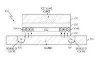
- FIG. 6is a cross-sectional view of a portion of a dual-bit memory cell 150 in accordance with an exemplary embodiment of the present invention.
- the dual-bit memory cell 150comprises a substrate 154 having a first buried junction (e.g., source) region 160 and a second buried junction (e.g., drain) region 161 formed within substrate 154 in self-alignment with the memory device 150 , a first insulator layer 162 disposed over the substrate 154 , a pair of charge storage layers 164 A, 164 B each being disposed over the first insulator layer 162 , a second insulator layer 166 disposed over the charge storage regions 164 A, 164 B, an isolation region 170 disposed between the first insulator layer 162 and the second insulator layer 166 and also disposed between charge storage regions 164 A, 164 B, and a control gate 168 disposed over the second insulator layer 166 .
- a first metal silicide contact(not shown) can be disposed
- the charge storage regions 164 A, 164 Bare physically and electrically separated by the isolation region 170 which is disposed between the charge storage regions 164 A, 164 B such that charge (e.g., electrons) can only be injected into the charge storage regions 164 A, 164 B.
- the control gate 168may comprise polysilicon
- the charge storage regions 164 A, 164 Bmay comprise nitride, such as silicon-rich nitride, aluminum oxide, polysilicon, low K dielectric or other equivalent charge trapping materials
- the isolation region 170may comprise, for example, an oxide.
- the dielectric stackmay comprise, for example, an oxide-nitride-oxide (ONO) stack, an oxide-silicon rich nitride-oxide (ORO) stack, an oxide-poly-oxide (OSO) stack, an oxide-nitride-oxide-nitride-oxide (ONONO) stack, an oxide-silicon rich nitride-oxide-silicon rich nitride-oxide (ORORO) stack, etc.
- OEOoxide-nitride-oxide
- OROoxide-poly-oxide
- OSOoxide-nitride-oxide-nitride-oxide
- ONONOoxide-silicon rich nitride-oxide-silicon rich nitride-oxide
- OROROoxide-silicon rich nitride-oxide-silicon rich nitride-oxide
- techniques for erasing the dual-bit memory cell 150are provided in which electrons can be injected into at least one of the charge storage regions 164 A, B to erase the memory cell 150 .
- FIG. 7is a cross-sectional view of a portion of a dual-bit memory cell 150 which illustrates a Fowler-Nordheim (FN) erase operation in accordance with an exemplary embodiment of the present invention.
- FNFowler-Nordheim
- electrons ( ⁇ )are only injected or tunneled into at least one of the charge storage regions 164 A, 164 B of the memory cell 150 .
- Fowler-Nordheim (FN) electron tunnelingcan be accomplished, for example, by floating or grounding the buried junction regions 60 , 61 , grounding the substrate 154 and then applying a relatively high positive bias voltage to the control gate 168 to pull electrons from the substrate 154 into at least one or both of the charge storage regions 164 A, 164 B.
- the charge storage regions 164 A, 164 Bcan be physically and electrically separated by the isolation region 170 disposed between the charge storage regions 164 A, 164 B such that electrons are only injected into the charge storage regions 164 A, 164 B and not into the isolation region 170 .
- the FN tunneling operationinvolves a relatively small amount of current and therefore consumes relatively low power.
- FIG. 8is a cross-sectional view of a portion of a dual-bit Memory cell 150 which illustrates a band-to-band hot hole (BTBHH) “program” operation in accordance with an exemplary embodiment of the present invention.
- the charge storage regions 164 A, 164 Bcan each initially hold electrons.
- holescan be injected into at least one of the two charge storage regions 164 A, 164 B of the memory cell 150 to neutralize the electrons ( ⁇ ) stored in the at least one of the charge storage regions 164 A, 164 B as bit 1 and/or bit 2 .
- the charge storage regions 164 A, 164 Bare physically and electrically separated by the isolation region 170 disposed between the charge storage regions 164 A, 164 B. As such, holes can only be injected into the charge storage regions 164 A, 164 B.
- FIG. 9is a cross-sectional view of a portion of a dual-bit memory cell 150 which illustrates an electron free isolation region 170 and electron free charge storage regions 164 A, 164 B in accordance with an exemplary embodiment of the present invention.
- the isolation region 170 and at least one of the charge storage regions 164 A, 164 Bare substantially charge free (e.g., no residual electrons ( ⁇ ) remain trapped in the isolation region 170 and at least one of the charge storage regions 164 A, 164 B) after the CCH “program” operation.
- the threshold voltage in isolation region 170is substantially the same as the threshold voltages in the charge storage layer regions 164 A, B.
Landscapes
- Engineering & Computer Science (AREA)
- Microelectronics & Electronic Packaging (AREA)
- Semiconductor Memories (AREA)
- Non-Volatile Memory (AREA)
Abstract
Description
- The present invention generally relates to memory devices, and more particularly relates to methods for erasing and programming a dual-bit memory device.
- Flash memory is a type of electronic memory media that can hold its data in the absence of operating power. Flash memory can be programmed, erased, and reprogrammed during its useful life (which may be up to one million write cycles for typical flash memory devices). Flash memory is becoming increasingly popular as a reliable, compact, and inexpensive nonvolatile memory in a number of consumer, commercial, and other applications. As electronic devices get smaller and smaller, it becomes desirable to increase the amount of data that can be stored per unit area on an integrated circuit memory cell, such as a flash memory unit.
- One conventional flash memory technology is based upon a memory cell that utilizes a charge trapping dielectric cell that is capable of storing two bits of data. Non-volatile memory designers have recently designed memory circuits that utilize two charge storage regions to store charge within a single silicon nitride layer. This type of non-volatile memory device is known as a dual-bit Flash electrically erasable and programmable read-only memory (EEPROM), which is available under the trademark MIRRORBIT™ from Advanced Micro Devices, Inc., Sunnyvale, Calif. In such an arrangement, one bit can be stored using a first charge storing region on one side of the silicon nitride layer, while a second bit can be stored using a second charge storing region on the other side of the same silicon nitride layer. For example, a left bit and right bit can be stored in physically different areas of the silicon nitride layer, near left and right regions of each memory cell, respectively. In comparison to a conventional EEPROM cell, a dual-bit memory cell can store twice as much information in a memory array of equal size.
FIG. 1 is a cross-sectional view of a conventional dual-bit memory cell 50. Thememory cell 50 has a dual-bit (bit1, bit2) architecture that allows twice as much storage capacity as a conventional EEPROM memory device.- The
conventional memory cell 50 includes asubstrate 54, afirst insulator layer 62 disposed over thesubstrate 54, a nitridecharge storage layer 64 disposed over thefirst insulator layer 62, asecond insulator layer 66 disposed over thecharge storage layer 64, and apolysilicon control gate 68 disposed over thesecond insulator layer 66. To produce an operable memory device, a first metal silicide contact (not shown) can be disposed onsubstrate 54, and thecontrol gate 66 can be capped with a second metal silicide contact (not shown). - In one implementation, the
substrate 54 is a P-type semiconductor substrate 54 having a first buriedjunction region 60 and a second buriedjunction region 61 formed withinsubstrate 54 in self-alignment with thememory cell 50. First buriedjunction region 60 and second buriedjunction region 61 are each formed from an N+ semiconductor material. Thecharge storage layer 64 is capable of holding a charge. Thefirst insulator layer 62, thecharge storage layer 64, and thesecond insulator layer 66 can be implemented using an oxide-nitride-oxide (ONO) configuration in which a nitridecharge storage layer 64 is sandwiched between two silicondioxide insulator layers charge storage layer 64 may utilize buried polysilicon islands as a charge trapping layer. Memory cell 50 can store two data bits: a left bit represented by the circle (bit1); and a right bit represented by the circle (bit2). In practice,memory cell 50 is generally symmetrical, thus first buriedjunction region 60 and second buriedjunction region 61 are interchangeable. In this regard, first buriedjunction region 60 may serve as the source region with respect to the right bit (bit2), while second buriedjunction region 61 may serve as the drain region with respect to the right bit (bit2). Conversely, second buriedjunction region 61 may serve as the source region with respect to the left bit (bit1), while first buriedjunction region 60 may serve as the drain region with respect to the left bit (bit1). A threshold voltage exists between thecontrol gate 66 and thesubstrate 54 to prevent leakage during functioning of the device.- While a single dual-
bit memory cell 50 is illustrated inFIG. 1 , it will be appreciated that any suitable number of the dual-bit memory cells 50 could be used to form a memory array, as described below with reference toFIG. 2 . FIG. 2 is a simplified diagram of a plurality of dual-bit memory cells arranged in accordance with a conventional array architecture200 (a practical array architecture can include thousands of dual-bit memory cells50).Array architecture 200 includes a number of buried bit lines formed in a semiconductor substrate as mentioned above.FIG. 2 depicts three buried bit lines (reference numbers array architecture 200.Array architecture 200 also includes a number of word lines that are utilized to control the gate voltage of the memory cells.FIG. 2 depicts four word lines (reference numbers FIG. 2 , charge storage layer, such as an ONO stack, resides between the bit lines and the word lines. The dashed lines inFIG. 2 represent two of the dual-bit memory cells in array architecture200: a first cell216 and a second cell218. Notably,bit line 204 is shared by first cell216 and second cell218.Array architecture 200 is known as a virtual ground architecture because ground potential can be applied to any selected bit line and there need not be any bit lines with a fixed ground potential.- Control logic and circuitry (not shown) for
array architecture 200 governs the selection of memory cells, the application of voltage to theword lines bit lines bit lines FIG. 2 depicts three conductive metal lines (reference numbers - When charging up the
charge storage layer 64, one way to reduce or minimize power consumption is by using Fowler-Nordheim (FN) tunneling mechanism to inject electrons into thecharge storage layer 64 and thereby erase thememory cell 50. FIG. 3 is a cross-sectional view of the conventional dual-bit memory cell during a Fowler-Nordheim (FN) erase operation in which FN tunneling can be used to inject electrons into the nitridecharge storage layer 64. The basic structure of thememory cell 50 is described above with respect toFIG. 1 , and for sake of brevity will not be described again. The buriedjunction regions positive gate 68 bias voltage (e.g., 18 volts to 20 volts) pulls electrons (Θ) from thegrounded substrate 54 into thecharge storage layer 64 such that thecharge storage layer 64 is evenly charged with electrons (Θ). This FN tunneling operation involves a relatively small amount of current and therefore consumes relatively low power.FIG. 4 is a cross-sectional view of the structure of the conventional dual-bit memory cell during band-to-band hot hole (BTBHH) programming operation. The basic structure of thememory cell 50 is described above with respect toFIG. 1 , and for sake of brevity will not be described again. This particular bias configuration, can be used to inject hot holes (electrically positively charged) into the right hand side (bit2) of the nitridecharge storage layer 64 to neutralize electrons stored atbit 2 thereby “programming”bit 2 of thememory cell 50. The right bit (bit2) is programmed by applying a relatively high negative voltage togate 68 via the appropriately selected word line, floating the bit line corresponding to first buried junction region60 (which serves as the source in this case), and applying a medium positive bias voltage to the bit line corresponding to second buried junction region61 (which serves as the drain in this case). This injects holes into thenitride layer 64 to neutralize electrons trapped in thenitride layer 64 atbit 2. Although not shown, by switching the drain/source biasing condition, holes can be injected intobit 1. The left bit (bit1) is programmed by applying a relatively high negative voltage togate 68 via the appropriately selected word line, floating the bit line corresponding to second buried junction region61 (which serves as the source in this case), and applying a medium positive bias voltage to the bit line corresponding to first buried junction region60 (which serves as the drain in this case).FIG. 5 is a cross-sectional view of a conventional dual-bit memory cell 50 which illustrates residual electrons (Θ) that result in the center of thecharge storage layer 64 as a result of the program operation. In an ideal situation, after programming one of thebits memory cell 50, the other one of thebits charge storage layer 64 during the charge up operation ofFIG. 3 . In other words, in an ideal situation, whenbit 1 is programmed, one-half of the electrons atbit 1 would be neutralized, whenbit 2 is programmed, one-half of the electrons atbit 2 would be neutralized, and if bothbit charge storage layer 64 would be neutralized. However, as illustrated inFIG. 5 , band-to-band hot hole (BTBHH) programming leaves residual electrons (Θ) in the center portion of thecharge storage layer 64 since hot holes can not be injected that far and therefore residual electrons (Θ) can not be neutralized. This results in degraded device operation or performance and reliability problems. For example, the residual electrons (Θ) in the center portion of thecharge storage layer 64 can interfere with transistor operation since the transistor is no longer uniform because the threshold voltage at the center of thecharge storage layer 64 would be different than the threshold voltages near the ends of thecharge storage layer 64.- Notwithstanding these advances, it would be desirable to provide improved techniques for erasing and/or programming a dual-bit memory cell. Furthermore, other desirable features and characteristics of the present invention will become apparent from the subsequent detailed description of the invention and the appended claims, taken in conjunction with the accompanying drawings and this background of the invention.
- Techniques for programming and erasing a memory are provided.
- According to one embodiment, techniques for erasing a memory can be provided in which electrons can be injected into at least one charge storage region to erase the memory. The charge storage regions can be physically and electrically separated by an isolation region disposed between the charge storage regions such that electrons are only injected into at least one of the charge storage regions. Electron injection can be accomplished, for example, by Fowler-Nordheim (FN) electron tunneling technique in which electrons are tunneled into at least one of the charge storage regions to erase the memory. Fowler-Nordheim (FN) electron tunneling can be accomplished, for example, by grounding a substrate and then applying a positive bias voltage to a gate to pull electrons from the substrate into at least one of the charge storage regions.
- According to another embodiment, techniques for programming a memory can be provided in which holes can be injected into at least one of the charge storage regions, which initially holds electrons, to program the memory. The charge storage regions can be physically and electrically separated by an isolation region disposed between the charge storage regions such that holes are only injected into at least one of the charge storage regions. Injecting holes into the at least one of the charge storage regions neutralizes electrons held in the at least one of the charge storage regions. Hole injection can be accomplished, for example, using a band-to-band hot hole (BTBHH) programming technique which involves applying a positive bias voltage to a source or drain region of a substrate and applying a negative voltage to a gate to pull holes from either the source region or the drain region into at least one of the charge storage regions. After programming, the isolation region and at least one of the charge storage regions are substantially charge free such that substantially no residual electrons remain in the isolation region and the at least one of the charge storage regions.
- The present invention will hereinafter be described in conjunction with the following drawing figures, wherein like numerals denote like cells, and wherein
FIG. 1 is a simplified cross-sectional view of a conventional dual-bit memory cell;FIG. 2 is a simplified diagram of a plurality of dual-bit memory cells arranged in accordance with a conventional array architecture;FIG. 3 is a cross-sectional view of the conventional dual-bit memory cell during a Fowler-Nordheim (FN) erase operation;FIG. 4 is a cross-sectional view of the structure of the conventional dual-bit Memory cell during band-to-band hot hole (BTBHH) programming operation;FIG. 5 is a cross-sectional view of a conventional dual-bit memory cell which illustrates residual electrons (Θ) that remain in the center of the charge storage layer after the band-to-band hot hole (BTBHH) programming operation;FIG. 6 is a cross-sectional view of a portion of a dual-bit memory cell;FIG. 7 is a cross-sectional view of the portion of the dual-bit memory cell which illustrates a Fowler-Nordheim (FN) erase operation in accordance with an exemplary embodiment of the present invention;FIG. 8 is a cross-sectional view of the portion of the dual-bit memory cell which illustrates a band-to-band hot hole (BTBHH) program operation in accordance with an exemplary embodiment of the present invention; andFIG. 9 is a cross-sectional view of the portion of the dual-bit memory cell which illustrates an electron free charge storage layer that results after BTBHH program operation in accordance with an exemplary embodiment of the present invention.- The following detailed description of the invention is merely exemplary in nature and is not intended to limit the invention or the application and uses of the invention. Furthermore, there is no intention to be bound by any theory presented in the preceding background of the invention or the following detailed description of the invention.
FIGS. 6-9 describe an erasing operation and a programming operation in a dual-bit memory cell 150 in which two charge storage regions are physically and electrically separated from one another by anisolation region 170.FIG. 6 is a cross-sectional view of a portion of a dual-bit memory cell 150 in accordance with an exemplary embodiment of the present invention. The dual-bit memory cell 150 comprises asubstrate 154 having a first buried junction (e.g., source)region 160 and a second buried junction (e.g., drain)region 161 formed withinsubstrate 154 in self-alignment with thememory device 150, afirst insulator layer 162 disposed over thesubstrate 154, a pair ofcharge storage layers first insulator layer 162, asecond insulator layer 166 disposed over thecharge storage regions isolation region 170 disposed between thefirst insulator layer 162 and thesecond insulator layer 166 and also disposed betweencharge storage regions control gate 168 disposed over thesecond insulator layer 166. A first metal silicide contact (not shown) can be disposed onsubstrate 154, and thecontrol gate 166 can be capped with a second metal silicide contact (not shown).- The
charge storage regions isolation region 170 which is disposed between thecharge storage regions charge storage regions control gate 168 may comprise polysilicon, thecharge storage regions isolation region 170 may comprise, for example, an oxide. Thus, depending on the implementation, the dielectric stack may comprise, for example, an oxide-nitride-oxide (ONO) stack, an oxide-silicon rich nitride-oxide (ORO) stack, an oxide-poly-oxide (OSO) stack, an oxide-nitride-oxide-nitride-oxide (ONONO) stack, an oxide-silicon rich nitride-oxide-silicon rich nitride-oxide (ORORO) stack, etc. - According to one embodiment, techniques for erasing the dual-
bit memory cell 150 are provided in which electrons can be injected into at least one of thecharge storage regions 164 A, B to erase thememory cell 150. FIG. 7 is a cross-sectional view of a portion of a dual-bit memory cell 150 which illustrates a Fowler-Nordheim (FN) erase operation in accordance with an exemplary embodiment of the present invention. According to this Fowler-Nordheim (FN) erase operation, electrons (Θ) are only injected or tunneled into at least one of thecharge storage regions memory cell 150. Fowler-Nordheim (FN) electron tunneling can be accomplished, for example, by floating or grounding the buriedjunction regions substrate 154 and then applying a relatively high positive bias voltage to thecontrol gate 168 to pull electrons from thesubstrate 154 into at least one or both of thecharge storage regions charge storage regions isolation region 170 disposed between thecharge storage regions charge storage regions isolation region 170. The FN tunneling operation involves a relatively small amount of current and therefore consumes relatively low power.FIG. 8 is a cross-sectional view of a portion of a dual-bit Memory cell 150 which illustrates a band-to-band hot hole (BTBHH) “program” operation in accordance with an exemplary embodiment of the present invention. Thecharge storage regions charge storage regions memory cell 150 to neutralize the electrons (Θ) stored in the at least one of thecharge storage regions bit 1 and/orbit 2. This can be accomplished, for example, by floating the first buried junction (e.g., source)region 160, applying a positive bias voltage (e.g., 5 volts) to the second buried junction (e.g., drain)region 161, and applying a negative voltage (e.g., −6 volts) to thecontrol gate 168 to pull holes fromregion 161 into one of thecharge storage regions charge storage regions isolation region 170 disposed between thecharge storage regions charge storage regions FIG. 9 is a cross-sectional view of a portion of a dual-bit memory cell 150 which illustrates an electronfree isolation region 170 and electron freecharge storage regions FIG. 5 , theisolation region 170 and at least one of thecharge storage regions isolation region 170 and at least one of thecharge storage regions FIG. 5 , device operation or performance can be improved and a more uniform and reliable transistor structure is provided. The threshold voltage inisolation region 170 is substantially the same as the threshold voltages in the chargestorage layer regions 164 A, B.- While at least one exemplary embodiment has been presented in the foregoing detailed description of the invention, it should be appreciated that a vast number of variations exist. It should also be appreciated that the exemplary embodiment or exemplary embodiments are only examples, and are not intended to limit the scope, applicability, or configuration of the invention in any way. Rather, the foregoing detailed description will provide those skilled in the art with a convenient road map for implementing an exemplary embodiment of the invention, it being understood that various changes may be made in the function and arrangement of cells described in an exemplary embodiment without departing from the scope of the invention as set forth in the appended claims and their legal equivalents.
Claims (36)
Priority Applications (7)
| Application Number | Priority Date | Filing Date | Title |
|---|---|---|---|
| US11/399,130US7394702B2 (en) | 2006-04-05 | 2006-04-05 | Methods for erasing and programming memory devices |
| TW096111970ATWI371101B (en) | 2006-04-05 | 2007-04-04 | Methods for erasing and programming memory devices and semiconductor device |
| KR1020087026872AKR101308692B1 (en) | 2006-04-05 | 2007-04-05 | Method for erasing and programming memory device |
| JP2009504339AJP2009532911A (en) | 2006-04-05 | 2007-04-05 | How to erase and write memory devices |
| EP07774953AEP2005436A2 (en) | 2006-04-05 | 2007-04-05 | Methods for erasing and programming memory devices |
| PCT/US2007/008683WO2007114955A2 (en) | 2006-04-05 | 2007-04-05 | Methods for erasing and programming memory devices |
| CN2007800148670ACN101432820B (en) | 2006-04-05 | 2007-04-05 | Method for erasing and programming memory devices |
Applications Claiming Priority (1)
| Application Number | Priority Date | Filing Date | Title |
|---|---|---|---|
| US11/399,130US7394702B2 (en) | 2006-04-05 | 2006-04-05 | Methods for erasing and programming memory devices |
Publications (2)
| Publication Number | Publication Date |
|---|---|
| US20070247923A1true US20070247923A1 (en) | 2007-10-25 |
| US7394702B2 US7394702B2 (en) | 2008-07-01 |
Family
ID=38564154
Family Applications (1)
| Application Number | Title | Priority Date | Filing Date |
|---|---|---|---|
| US11/399,130ActiveUS7394702B2 (en) | 2006-04-05 | 2006-04-05 | Methods for erasing and programming memory devices |
Country Status (7)
| Country | Link |
|---|---|
| US (1) | US7394702B2 (en) |
| EP (1) | EP2005436A2 (en) |
| JP (1) | JP2009532911A (en) |
| KR (1) | KR101308692B1 (en) |
| CN (1) | CN101432820B (en) |
| TW (1) | TWI371101B (en) |
| WO (1) | WO2007114955A2 (en) |
Cited By (5)
| Publication number | Priority date | Publication date | Assignee | Title |
|---|---|---|---|---|
| US20080031053A1 (en)* | 2006-08-01 | 2008-02-07 | Macronix International Co., Ltd. | A method for improving memory device cycling endurance by providing additional pulse |
| US20080224275A1 (en)* | 2007-03-15 | 2008-09-18 | Spansion Llc | Semiconductor device and method for manufacturing thereof |
| US20100221851A1 (en)* | 2006-07-26 | 2010-09-02 | Macronix International Co., Ltd. | Test structure and method for detecting charge effects during semiconductor processing |
| JP2016500479A (en)* | 2012-12-14 | 2016-01-12 | スパンション エルエルシー | Formation of transistor and split gate charge trap memory cells using disposable gate caps |
| US20160172372A1 (en)* | 2014-12-10 | 2016-06-16 | Ju-Mi YUN | Semiconductor devices |
Families Citing this family (9)
| Publication number | Priority date | Publication date | Assignee | Title |
|---|---|---|---|---|
| TWI300931B (en)* | 2006-06-20 | 2008-09-11 | Macronix Int Co Ltd | Method of operating non-volatile memory device |
| US7916550B2 (en)* | 2006-11-17 | 2011-03-29 | Macronix International Co., Ltd. | Method and apparatus for operating nonvolatile memory with floating voltage at one of the source and drain regions |
| US7652923B2 (en)* | 2007-02-02 | 2010-01-26 | Macronix International Co., Ltd. | Semiconductor device and memory and method of operating thereof |
| JP5425378B2 (en)* | 2007-07-30 | 2014-02-26 | スパンション エルエルシー | Manufacturing method of semiconductor device |
| KR100877483B1 (en)* | 2007-10-04 | 2009-01-07 | 주식회사 동부하이텍 | Flash memory device and manufacturing method thereof |
| TWI442400B (en) | 2010-02-22 | 2014-06-21 | Acer Inc | Memory component operation method |
| US9368606B2 (en) | 2012-12-14 | 2016-06-14 | Cypress Semiconductor Corporation | Memory first process flow and device |
| US10014380B2 (en) | 2012-12-14 | 2018-07-03 | Cypress Semiconductor Corporation | Memory first process flow and device |
| WO2024210502A1 (en)* | 2023-04-05 | 2024-10-10 | 서울대학교산학협력단 | Charge storage type tunneling transistor device, manufacturing device therefor, and boolean logic operation method therefor |
Citations (13)
| Publication number | Priority date | Publication date | Assignee | Title |
|---|---|---|---|---|
| US6242306B1 (en)* | 2000-07-28 | 2001-06-05 | Advanced Micro Devices | Dual bit isolation scheme for flash memory devices having polysilicon floating gates |
| US6261904B1 (en)* | 2000-02-10 | 2001-07-17 | Advanced Micro Devices, Inc. | Dual bit isolation scheme for flash devices |
| US6355514B1 (en)* | 2000-02-10 | 2002-03-12 | Advanced Micro Devices, Inc. | Dual bit isolation scheme for flash devices |
| US6480414B1 (en)* | 2000-01-11 | 2002-11-12 | Winbond Electronics Corp. | Multi-level memory cell |
| US6639271B1 (en)* | 2001-12-20 | 2003-10-28 | Advanced Micro Devices, Inc. | Fully isolated dielectric memory cell structure for a dual bit nitride storage device and process for making same |
| US6735123B1 (en)* | 2002-06-07 | 2004-05-11 | Advanced Micro Devices, Inc. | High density dual bit flash memory cell with non planar structure |
| US6768160B1 (en)* | 2003-01-28 | 2004-07-27 | Advanced Micro Devices, Inc. | Non-volatile memory cell and method of programming for improved data retention |
| US20050104117A1 (en)* | 2003-11-17 | 2005-05-19 | Thomas Mikolajick | Charge-trapping memory device and methods for operating and manufacturing the cell |
| US20050105341A1 (en)* | 2003-11-04 | 2005-05-19 | Micron Technology, Inc. | NROM flash memory with self-aligned structural charge separation |
| US20050116281A1 (en)* | 2003-12-01 | 2005-06-02 | Chin-Tien Yang | Multilayered dual bit memory device with improved write/erase characteristics and method of manufacturing |
| US6906959B2 (en)* | 2002-11-27 | 2005-06-14 | Advanced Micro Devices, Inc. | Method and system for erasing a nitride memory device |
| US6914820B1 (en)* | 2002-05-06 | 2005-07-05 | Multi Level Memory Technology | Erasing storage nodes in a bi-directional nonvolatile memory cell |
| US6958510B2 (en)* | 2001-11-14 | 2005-10-25 | Stmicroelectronics S.R.L. | Process for fabricating a dual charge storage location memory cell |
Family Cites Families (6)
| Publication number | Priority date | Publication date | Assignee | Title |
|---|---|---|---|---|
| US6768165B1 (en) | 1997-08-01 | 2004-07-27 | Saifun Semiconductors Ltd. | Two bit non-volatile electrically erasable and programmable semiconductor memory cell utilizing asymmetrical charge trapping |
| US6538925B2 (en) | 2000-11-09 | 2003-03-25 | Innotech Corporation | Semiconductor memory device, method of manufacturing the same and method of driving the same |
| US20030062567A1 (en) | 2001-09-28 | 2003-04-03 | Wei Zheng | Non volatile dielectric memory cell structure with high dielectric constant capacitive coupling layer |
| US6795342B1 (en)* | 2002-12-02 | 2004-09-21 | Advanced Micro Devices, Inc. | System for programming a non-volatile memory cell |
| CN1677568A (en)* | 2004-04-01 | 2005-10-05 | 上海宏力半导体制造有限公司 | Flash-storage two-position memory cell structure |
| CN1719617A (en)* | 2005-07-08 | 2006-01-11 | 北京大学 | Two-bit flash memory unit storing information at both ends and reading method thereof |
- 2006
- 2006-04-05USUS11/399,130patent/US7394702B2/enactiveActive
- 2007
- 2007-04-04TWTW096111970Apatent/TWI371101B/ennot_activeIP Right Cessation
- 2007-04-05CNCN2007800148670Apatent/CN101432820B/enactiveActive
- 2007-04-05WOPCT/US2007/008683patent/WO2007114955A2/enactiveApplication Filing
- 2007-04-05JPJP2009504339Apatent/JP2009532911A/enactivePending
- 2007-04-05KRKR1020087026872Apatent/KR101308692B1/ennot_activeExpired - Fee Related
- 2007-04-05EPEP07774953Apatent/EP2005436A2/ennot_activeWithdrawn
Patent Citations (15)
| Publication number | Priority date | Publication date | Assignee | Title |
|---|---|---|---|---|
| US6480414B1 (en)* | 2000-01-11 | 2002-11-12 | Winbond Electronics Corp. | Multi-level memory cell |
| US6261904B1 (en)* | 2000-02-10 | 2001-07-17 | Advanced Micro Devices, Inc. | Dual bit isolation scheme for flash devices |
| US6355514B1 (en)* | 2000-02-10 | 2002-03-12 | Advanced Micro Devices, Inc. | Dual bit isolation scheme for flash devices |
| US6242306B1 (en)* | 2000-07-28 | 2001-06-05 | Advanced Micro Devices | Dual bit isolation scheme for flash memory devices having polysilicon floating gates |
| US6958510B2 (en)* | 2001-11-14 | 2005-10-25 | Stmicroelectronics S.R.L. | Process for fabricating a dual charge storage location memory cell |
| US6639271B1 (en)* | 2001-12-20 | 2003-10-28 | Advanced Micro Devices, Inc. | Fully isolated dielectric memory cell structure for a dual bit nitride storage device and process for making same |
| US6861307B2 (en)* | 2001-12-20 | 2005-03-01 | Advanced Micro Devices, Inc. | Fully isolated dielectric memory cell structure for a dual bit nitride storage device and process for making same |
| US6914820B1 (en)* | 2002-05-06 | 2005-07-05 | Multi Level Memory Technology | Erasing storage nodes in a bi-directional nonvolatile memory cell |
| US6735123B1 (en)* | 2002-06-07 | 2004-05-11 | Advanced Micro Devices, Inc. | High density dual bit flash memory cell with non planar structure |
| US6906959B2 (en)* | 2002-11-27 | 2005-06-14 | Advanced Micro Devices, Inc. | Method and system for erasing a nitride memory device |
| US6768160B1 (en)* | 2003-01-28 | 2004-07-27 | Advanced Micro Devices, Inc. | Non-volatile memory cell and method of programming for improved data retention |
| US20050105341A1 (en)* | 2003-11-04 | 2005-05-19 | Micron Technology, Inc. | NROM flash memory with self-aligned structural charge separation |
| US20050104117A1 (en)* | 2003-11-17 | 2005-05-19 | Thomas Mikolajick | Charge-trapping memory device and methods for operating and manufacturing the cell |
| US20050116281A1 (en)* | 2003-12-01 | 2005-06-02 | Chin-Tien Yang | Multilayered dual bit memory device with improved write/erase characteristics and method of manufacturing |
| US6956254B2 (en)* | 2003-12-01 | 2005-10-18 | Taiwan Semiconductor Manufacturing Company, Ltd. | Multilayered dual bit memory device with improved write/erase characteristics and method of manufacturing |
Cited By (13)
| Publication number | Priority date | Publication date | Assignee | Title |
|---|---|---|---|---|
| US20100221851A1 (en)* | 2006-07-26 | 2010-09-02 | Macronix International Co., Ltd. | Test structure and method for detecting charge effects during semiconductor processing |
| US8241928B2 (en)* | 2006-07-26 | 2012-08-14 | Macronix International Co., Ltd. | Test structure and method for detecting charge effects during semiconductor processing |
| US20090323428A1 (en)* | 2006-08-01 | 2009-12-31 | Macronix International Co., Ltd. | Method for improving memory device cycling endurance by providing additional pulses |
| US20080031053A1 (en)* | 2006-08-01 | 2008-02-07 | Macronix International Co., Ltd. | A method for improving memory device cycling endurance by providing additional pulse |
| US7596030B2 (en)* | 2006-08-01 | 2009-09-29 | Macronix International Co., Ltd. | Method for improving memory device cycling endurance by providing additional pulse |
| US7903471B2 (en) | 2006-08-01 | 2011-03-08 | Macronix International Co. Ltd. | Method for improving memory device cycling endurance by providing additional pulses |
| US20080224275A1 (en)* | 2007-03-15 | 2008-09-18 | Spansion Llc | Semiconductor device and method for manufacturing thereof |
| US8994093B2 (en)* | 2007-03-15 | 2015-03-31 | Spansion Llc | Semiconductor device with ONO film |
| US9515081B2 (en) | 2007-03-15 | 2016-12-06 | Cypress Semiconductor Corporation | Semiconductor device and method for manufacturing thereof |
| JP2016500479A (en)* | 2012-12-14 | 2016-01-12 | スパンション エルエルシー | Formation of transistor and split gate charge trap memory cells using disposable gate caps |
| US20160172372A1 (en)* | 2014-12-10 | 2016-06-16 | Ju-Mi YUN | Semiconductor devices |
| US9754959B2 (en)* | 2014-12-10 | 2017-09-05 | Samsung Electronics Co., Ltd. | Non-volatile semiconductor devices |
| US9991281B2 (en) | 2014-12-10 | 2018-06-05 | Samsung Electronics Co., Ltd. | Semiconductor devices and methods of manufacturing the same |
Also Published As
| Publication number | Publication date |
|---|---|
| US7394702B2 (en) | 2008-07-01 |
| WO2007114955A2 (en) | 2007-10-11 |
| TW200746402A (en) | 2007-12-16 |
| JP2009532911A (en) | 2009-09-10 |
| KR20090006158A (en) | 2009-01-14 |
| CN101432820A (en) | 2009-05-13 |
| KR101308692B1 (en) | 2013-09-13 |
| EP2005436A2 (en) | 2008-12-24 |
| TWI371101B (en) | 2012-08-21 |
| WO2007114955A3 (en) | 2008-02-07 |
| CN101432820B (en) | 2012-11-28 |
Similar Documents
| Publication | Publication Date | Title |
|---|---|---|
| US7394702B2 (en) | Methods for erasing and programming memory devices | |
| US6671209B2 (en) | Erasing method for p-channel NROM | |
| US8344445B2 (en) | Non-volatile semiconductor memory cell with dual functions | |
| US7471564B2 (en) | Trapping storage flash memory cell structure with inversion source and drain regions | |
| US7515479B2 (en) | Nonvolatile semiconductor storage device and method for writing therein | |
| US8264884B2 (en) | Methods, circuits and systems for reading non-volatile memory cells | |
| US20070247924A1 (en) | Methods for erasing memory devices and multi-level programming memory device | |
| US6493262B1 (en) | Method for operating nonvolatile memory cells | |
| JP2007142398A (en) | Driving method of single layer polysilicon nonvolatile memory cell | |
| KR20020071706A (en) | Usage of word voltage assistance in twin MONOS cell during program and erase | |
| US6801456B1 (en) | Method for programming, erasing and reading a flash memory cell | |
| TWI243475B (en) | Byte-operational nonvolatile semiconductor memory device | |
| TW201301485A (en) | Dual-function non-volatile semiconductor memory unit | |
| KR20040031655A (en) | Single bit nonvolatile memory cell and methods for programming and erasing thereof | |
| US7911852B2 (en) | Nonvolatile semiconductor memory device and operation method thereof | |
| US7184316B2 (en) | Non-volatile memory cell array having common drain lines and method of operating the same | |
| US6834013B2 (en) | Method for programming and erasing non-volatile memory with nitride tunneling layer | |
| KR20000051783A (en) | Nonvolatile memory device | |
| US7200040B2 (en) | Method of operating p-channel memory | |
| US7948052B2 (en) | Dual-bit memory device having trench isolation material disposed near bit line contact areas | |
| US7554851B2 (en) | Reset method of non-volatile memory | |
| CN100461425C (en) | Operation method of P-type channel memory |
Legal Events
| Date | Code | Title | Description |
|---|---|---|---|
| AS | Assignment | Owner name:SPANSION LLC, CALIFORNIA Free format text:ASSIGNMENT OF ASSIGNORS INTEREST;ASSIGNORS:DING, MENG;LIU, ZHIZHENG;ZHENG, WEI;REEL/FRAME:018462/0946;SIGNING DATES FROM 20061026 TO 20061028 | |
| STCF | Information on status: patent grant | Free format text:PATENTED CASE | |
| AS | Assignment | Owner name:BARCLAYS BANK PLC,NEW YORK Free format text:SECURITY AGREEMENT;ASSIGNORS:SPANSION LLC;SPANSION INC.;SPANSION TECHNOLOGY INC.;AND OTHERS;REEL/FRAME:024522/0338 Effective date:20100510 Owner name:BARCLAYS BANK PLC, NEW YORK Free format text:SECURITY AGREEMENT;ASSIGNORS:SPANSION LLC;SPANSION INC.;SPANSION TECHNOLOGY INC.;AND OTHERS;REEL/FRAME:024522/0338 Effective date:20100510 | |
| FPAY | Fee payment | Year of fee payment:4 | |
| AS | Assignment | Owner name:SPANSION LLC, CALIFORNIA Free format text:RELEASE BY SECURED PARTY;ASSIGNOR:BARCLAYS BANK PLC;REEL/FRAME:035201/0159 Effective date:20150312 Owner name:SPANSION TECHNOLOGY LLC, CALIFORNIA Free format text:RELEASE BY SECURED PARTY;ASSIGNOR:BARCLAYS BANK PLC;REEL/FRAME:035201/0159 Effective date:20150312 Owner name:SPANSION INC., CALIFORNIA Free format text:RELEASE BY SECURED PARTY;ASSIGNOR:BARCLAYS BANK PLC;REEL/FRAME:035201/0159 Effective date:20150312 | |
| AS | Assignment | Owner name:MORGAN STANLEY SENIOR FUNDING, INC., NEW YORK Free format text:SECURITY INTEREST;ASSIGNORS:CYPRESS SEMICONDUCTOR CORPORATION;SPANSION LLC;REEL/FRAME:035240/0429 Effective date:20150312 | |
| AS | Assignment | Owner name:CYPRESS SEMICONDUCTOR CORPORATION, CALIFORNIA Free format text:ASSIGNMENT OF ASSIGNORS INTEREST;ASSIGNOR:SPANSION, LLC;REEL/FRAME:036039/0406 Effective date:20150601 | |
| FPAY | Fee payment | Year of fee payment:8 | |
| AS | Assignment | Owner name:MUFG UNION BANK, N.A., CALIFORNIA Free format text:ASSIGNMENT AND ASSUMPTION OF SECURITY INTEREST IN INTELLECTUAL PROPERTY;ASSIGNOR:MORGAN STANLEY SENIOR FUNDING, INC.;REEL/FRAME:050896/0366 Effective date:20190731 | |
| MAFP | Maintenance fee payment | Free format text:PAYMENT OF MAINTENANCE FEE, 12TH YEAR, LARGE ENTITY (ORIGINAL EVENT CODE: M1553); ENTITY STATUS OF PATENT OWNER: LARGE ENTITY Year of fee payment:12 | |
| AS | Assignment | Owner name:MORGAN STANLEY SENIOR FUNDING, INC., NEW YORK Free format text:CORRECTIVE ASSIGNMENT TO CORRECT THE 8647899 PREVIOUSLY RECORDED ON REEL 035240 FRAME 0429. ASSIGNOR(S) HEREBY CONFIRMS THE SECURITY INTERST;ASSIGNORS:CYPRESS SEMICONDUCTOR CORPORATION;SPANSION LLC;REEL/FRAME:058002/0470 Effective date:20150312 | |
| AS | Assignment | Owner name:SPANSION LLC, CALIFORNIA Free format text:RELEASE BY SECURED PARTY;ASSIGNOR:MUFG UNION BANK, N.A.;REEL/FRAME:059410/0438 Effective date:20200416 Owner name:CYPRESS SEMICONDUCTOR CORPORATION, CALIFORNIA Free format text:RELEASE BY SECURED PARTY;ASSIGNOR:MUFG UNION BANK, N.A.;REEL/FRAME:059410/0438 Effective date:20200416 | |
| AS | Assignment | Owner name:INFINEON TECHNOLOGIES LLC, CALIFORNIA Free format text:ASSIGNMENT OF ASSIGNORS INTEREST;ASSIGNOR:CYPRESS SEMICONDUCTOR CORPORATION;REEL/FRAME:059721/0467 Effective date:20200315 |