US20070246834A1 - Post passivation interconnection schemes on top of the IC chips - Google Patents
Post passivation interconnection schemes on top of the IC chipsDownload PDFInfo
- Publication number
- US20070246834A1 US20070246834A1US11/818,028US81802807AUS2007246834A1US 20070246834 A1US20070246834 A1US 20070246834A1US 81802807 AUS81802807 AUS 81802807AUS 2007246834 A1US2007246834 A1US 2007246834A1
- Authority
- US
- United States
- Prior art keywords
- layer
- circuit
- passivation
- metal
- metallization structure
- Prior art date
- Legal status (The legal status is an assumption and is not a legal conclusion. Google has not performed a legal analysis and makes no representation as to the accuracy of the status listed.)
- Granted
Links
- 238000002161passivationMethods0.000titleclaimsabstractdescription206
- 239000000758substrateSubstances0.000claimsabstractdescription59
- 239000004065semiconductorSubstances0.000claimsabstractdescription35
- 229910052751metalInorganic materials0.000claimsdescription202
- 239000002184metalSubstances0.000claimsdescription202
- 238000001465metallisationMethods0.000claimsdescription55
- 229920000642polymerPolymers0.000claimsdescription37
- RYGMFSIKBFXOCR-UHFFFAOYSA-NCopperChemical compound[Cu]RYGMFSIKBFXOCR-UHFFFAOYSA-N0.000claimsdescription29
- 229910052802copperInorganic materials0.000claimsdescription29
- 239000010949copperSubstances0.000claimsdescription29
- XUIMIQQOPSSXEZ-UHFFFAOYSA-NSiliconChemical compound[Si]XUIMIQQOPSSXEZ-UHFFFAOYSA-N0.000claimsdescription25
- 229910052710siliconInorganic materials0.000claimsdescription25
- 239000010703siliconSubstances0.000claimsdescription25
- PCHJSUWPFVWCPO-UHFFFAOYSA-NgoldChemical compound[Au]PCHJSUWPFVWCPO-UHFFFAOYSA-N0.000claimsdescription22
- 229910052737goldInorganic materials0.000claimsdescription22
- 239000010931goldSubstances0.000claimsdescription22
- KDLHZDBZIXYQEI-UHFFFAOYSA-NPalladiumChemical compound[Pd]KDLHZDBZIXYQEI-UHFFFAOYSA-N0.000claimsdescription16
- PXHVJJICTQNCMI-UHFFFAOYSA-NNickelChemical compound[Ni]PXHVJJICTQNCMI-UHFFFAOYSA-N0.000claimsdescription10
- 229910052709silverInorganic materials0.000claimsdescription9
- 239000004332silverSubstances0.000claimsdescription9
- 229910052763palladiumInorganic materials0.000claimsdescription8
- 229910052759nickelInorganic materials0.000claimsdescription5
- 150000004767nitridesChemical class0.000claimsdescription5
- 238000000034methodMethods0.000abstractdescription46
- XAGFODPZIPBFFR-UHFFFAOYSA-NaluminiumChemical compound[Al]XAGFODPZIPBFFR-UHFFFAOYSA-N0.000description38
- 238000009826distributionMethods0.000description26
- 230000008569processEffects0.000description24
- 229910052782aluminiumInorganic materials0.000description10
- 230000004888barrier functionEffects0.000description10
- 238000013461designMethods0.000description10
- 238000009713electroplatingMethods0.000description9
- 239000000463materialSubstances0.000description9
- 230000009467reductionEffects0.000description9
- 239000004642PolyimideSubstances0.000description8
- 238000000151depositionMethods0.000description8
- 150000002739metalsChemical class0.000description8
- 229920002120photoresistant polymerPolymers0.000description8
- 229920001721polyimidePolymers0.000description8
- 229910000679solderInorganic materials0.000description8
- 230000008021depositionEffects0.000description7
- 238000005137deposition processMethods0.000description7
- BQCADISMDOOEFD-UHFFFAOYSA-NSilverChemical compound[Ag]BQCADISMDOOEFD-UHFFFAOYSA-N0.000description6
- 230000001419dependent effectEffects0.000description5
- 238000010586diagramMethods0.000description5
- 238000005530etchingMethods0.000description5
- 239000010970precious metalSubstances0.000description5
- 230000008901benefitEffects0.000description4
- 238000004519manufacturing processMethods0.000description4
- 230000003071parasitic effectEffects0.000description4
- 239000000126substanceSubstances0.000description4
- 229910052581Si3N4Inorganic materials0.000description3
- VYPSYNLAJGMNEJ-UHFFFAOYSA-NSilicium dioxideChemical compoundO=[Si]=OVYPSYNLAJGMNEJ-UHFFFAOYSA-N0.000description3
- 238000013459approachMethods0.000description3
- 238000011109contaminationMethods0.000description3
- 230000008878couplingEffects0.000description3
- 238000010168coupling processMethods0.000description3
- 238000005859coupling reactionMethods0.000description3
- 239000012212insulatorSubstances0.000description3
- 150000002500ionsChemical class0.000description3
- -1moistureChemical class0.000description3
- 238000000623plasma-assisted chemical vapour depositionMethods0.000description3
- HQVNEWCFYHHQES-UHFFFAOYSA-Nsilicon nitrideChemical compoundN12[Si]34N5[Si]62N3[Si]51N64HQVNEWCFYHHQES-UHFFFAOYSA-N0.000description3
- 238000004544sputter depositionMethods0.000description3
- 239000002699waste materialSubstances0.000description3
- IJGRMHOSHXDMSA-UHFFFAOYSA-NAtomic nitrogenChemical compoundN#NIJGRMHOSHXDMSA-UHFFFAOYSA-N0.000description2
- JPVYNHNXODAKFH-UHFFFAOYSA-NCu2+Chemical compound[Cu+2]JPVYNHNXODAKFH-UHFFFAOYSA-N0.000description2
- 229910001111Fine metalInorganic materials0.000description2
- UMIVXZPTRXBADB-UHFFFAOYSA-NbenzocyclobuteneChemical compoundC1=CC=C2CCC2=C1UMIVXZPTRXBADB-UHFFFAOYSA-N0.000description2
- 230000015572biosynthetic processEffects0.000description2
- 239000003990capacitorSubstances0.000description2
- 239000011248coating agentSubstances0.000description2
- 238000000576coating methodMethods0.000description2
- 239000002131composite materialSubstances0.000description2
- 229910001431copper ionInorganic materials0.000description2
- 239000003989dielectric materialSubstances0.000description2
- 239000011521glassSubstances0.000description2
- 229910010272inorganic materialInorganic materials0.000description2
- 239000011147inorganic materialSubstances0.000description2
- 238000012986modificationMethods0.000description2
- 230000004048modificationEffects0.000description2
- 239000002245particleSubstances0.000description2
- 238000000059patterningMethods0.000description2
- 238000000206photolithographyMethods0.000description2
- 238000005498polishingMethods0.000description2
- 229910052723transition metalInorganic materials0.000description2
- 150000003624transition metalsChemical class0.000description2
- 238000001039wet etchingMethods0.000description2
- 229910000838Al alloyInorganic materials0.000description1
- 239000004593EpoxySubstances0.000description1
- BOTDANWDWHJENH-UHFFFAOYSA-NTetraethyl orthosilicateChemical compoundCCO[Si](OCC)(OCC)OCCBOTDANWDWHJENH-UHFFFAOYSA-N0.000description1
- ATJFFYVFTNAWJD-UHFFFAOYSA-NTinChemical compound[Sn]ATJFFYVFTNAWJD-UHFFFAOYSA-N0.000description1
- 230000005540biological transmissionEffects0.000description1
- 238000005229chemical vapour depositionMethods0.000description1
- 229910052804chromiumInorganic materials0.000description1
- 238000007796conventional methodMethods0.000description1
- QRJOYPHTNNOAOJ-UHFFFAOYSA-Ncopper goldChemical compound[Cu].[Au]QRJOYPHTNNOAOJ-UHFFFAOYSA-N0.000description1
- 238000005336crackingMethods0.000description1
- 238000001312dry etchingMethods0.000description1
- 230000000694effectsEffects0.000description1
- 230000008030eliminationEffects0.000description1
- 238000003379elimination reactionMethods0.000description1
- 238000005538encapsulationMethods0.000description1
- 238000005516engineering processMethods0.000description1
- 229940104869fluorosilicateDrugs0.000description1
- 238000009413insulationMethods0.000description1
- 239000007788liquidSubstances0.000description1
- 238000001459lithographyMethods0.000description1
- 239000007769metal materialSubstances0.000description1
- 229910052757nitrogenInorganic materials0.000description1
- 239000011368organic materialSubstances0.000description1
- 238000004806packaging method and processMethods0.000description1
- 230000035515penetrationEffects0.000description1
- 238000005268plasma chemical vapour depositionMethods0.000description1
- 229920000052poly(p-xylylene)Polymers0.000description1
- 229910021420polycrystalline siliconInorganic materials0.000description1
- 229920006254polymer filmPolymers0.000description1
- 229920005591polysiliconPolymers0.000description1
- 238000012545processingMethods0.000description1
- 238000007650screen-printingMethods0.000description1
- 230000035945sensitivityEffects0.000description1
- 235000012239silicon dioxideNutrition0.000description1
- 239000000377silicon dioxideSubstances0.000description1
- 229910052814silicon oxideInorganic materials0.000description1
- 229920002379silicone rubberPolymers0.000description1
- 229910001415sodium ionInorganic materials0.000description1
Images


Classifications
- H—ELECTRICITY
- H01—ELECTRIC ELEMENTS
- H01L—SEMICONDUCTOR DEVICES NOT COVERED BY CLASS H10
- H01L23/00—Details of semiconductor or other solid state devices
- H01L23/58—Structural electrical arrangements for semiconductor devices not otherwise provided for, e.g. in combination with batteries
- H01L23/62—Protection against overvoltage, e.g. fuses, shunts
- H—ELECTRICITY
- H01—ELECTRIC ELEMENTS
- H01L—SEMICONDUCTOR DEVICES NOT COVERED BY CLASS H10
- H01L23/00—Details of semiconductor or other solid state devices
- H01L23/28—Encapsulations, e.g. encapsulating layers, coatings, e.g. for protection
- H01L23/31—Encapsulations, e.g. encapsulating layers, coatings, e.g. for protection characterised by the arrangement or shape
- H01L23/3157—Partial encapsulation or coating
- H01L23/3192—Multilayer coating
- H—ELECTRICITY
- H01—ELECTRIC ELEMENTS
- H01L—SEMICONDUCTOR DEVICES NOT COVERED BY CLASS H10
- H01L23/00—Details of semiconductor or other solid state devices
- H01L23/52—Arrangements for conducting electric current within the device in operation from one component to another, i.e. interconnections, e.g. wires, lead frames
- H01L23/522—Arrangements for conducting electric current within the device in operation from one component to another, i.e. interconnections, e.g. wires, lead frames including external interconnections consisting of a multilayer structure of conductive and insulating layers inseparably formed on the semiconductor body
- H01L23/528—Layout of the interconnection structure
- H01L23/5283—Cross-sectional geometry
- H—ELECTRICITY
- H01—ELECTRIC ELEMENTS
- H01L—SEMICONDUCTOR DEVICES NOT COVERED BY CLASS H10
- H01L23/00—Details of semiconductor or other solid state devices
- H01L23/52—Arrangements for conducting electric current within the device in operation from one component to another, i.e. interconnections, e.g. wires, lead frames
- H01L23/522—Arrangements for conducting electric current within the device in operation from one component to another, i.e. interconnections, e.g. wires, lead frames including external interconnections consisting of a multilayer structure of conductive and insulating layers inseparably formed on the semiconductor body
- H01L23/532—Arrangements for conducting electric current within the device in operation from one component to another, i.e. interconnections, e.g. wires, lead frames including external interconnections consisting of a multilayer structure of conductive and insulating layers inseparably formed on the semiconductor body characterised by the materials
- H01L23/53204—Conductive materials
- H01L23/53209—Conductive materials based on metals, e.g. alloys, metal silicides
- H01L23/53228—Conductive materials based on metals, e.g. alloys, metal silicides the principal metal being copper
- H01L23/53238—Additional layers associated with copper layers, e.g. adhesion, barrier, cladding layers
- H—ELECTRICITY
- H01—ELECTRIC ELEMENTS
- H01L—SEMICONDUCTOR DEVICES NOT COVERED BY CLASS H10
- H01L23/00—Details of semiconductor or other solid state devices
- H01L23/52—Arrangements for conducting electric current within the device in operation from one component to another, i.e. interconnections, e.g. wires, lead frames
- H01L23/522—Arrangements for conducting electric current within the device in operation from one component to another, i.e. interconnections, e.g. wires, lead frames including external interconnections consisting of a multilayer structure of conductive and insulating layers inseparably formed on the semiconductor body
- H01L23/532—Arrangements for conducting electric current within the device in operation from one component to another, i.e. interconnections, e.g. wires, lead frames including external interconnections consisting of a multilayer structure of conductive and insulating layers inseparably formed on the semiconductor body characterised by the materials
- H01L23/53204—Conductive materials
- H01L23/53209—Conductive materials based on metals, e.g. alloys, metal silicides
- H01L23/53242—Conductive materials based on metals, e.g. alloys, metal silicides the principal metal being a noble metal, e.g. gold
- H01L23/53252—Additional layers associated with noble-metal layers, e.g. adhesion, barrier, cladding layers
- H—ELECTRICITY
- H01—ELECTRIC ELEMENTS
- H01L—SEMICONDUCTOR DEVICES NOT COVERED BY CLASS H10
- H01L2924/00—Indexing scheme for arrangements or methods for connecting or disconnecting semiconductor or solid-state bodies as covered by H01L24/00
- H01L2924/0001—Technical content checked by a classifier
- H01L2924/0002—Not covered by any one of groups H01L24/00, H01L24/00 and H01L2224/00
- H—ELECTRICITY
- H01—ELECTRIC ELEMENTS
- H01L—SEMICONDUCTOR DEVICES NOT COVERED BY CLASS H10
- H01L2924/00—Indexing scheme for arrangements or methods for connecting or disconnecting semiconductor or solid-state bodies as covered by H01L24/00
- H01L2924/19—Details of hybrid assemblies other than the semiconductor or other solid state devices to be connected
- H01L2924/1901—Structure
- H01L2924/1904—Component type
- H01L2924/19041—Component type being a capacitor
- H—ELECTRICITY
- H01—ELECTRIC ELEMENTS
- H01L—SEMICONDUCTOR DEVICES NOT COVERED BY CLASS H10
- H01L2924/00—Indexing scheme for arrangements or methods for connecting or disconnecting semiconductor or solid-state bodies as covered by H01L24/00
- H01L2924/30—Technical effects
- H01L2924/301—Electrical effects
- H01L2924/3011—Impedance
- H—ELECTRICITY
- H10—SEMICONDUCTOR DEVICES; ELECTRIC SOLID-STATE DEVICES NOT OTHERWISE PROVIDED FOR
- H10D—INORGANIC ELECTRIC SEMICONDUCTOR DEVICES
- H10D89/00—Aspects of integrated devices not covered by groups H10D84/00 - H10D88/00
- H10D89/60—Integrated devices comprising arrangements for electrical or thermal protection, e.g. protection circuits against electrostatic discharge [ESD]
- H10D89/601—Integrated devices comprising arrangements for electrical or thermal protection, e.g. protection circuits against electrostatic discharge [ESD] for devices having insulated gate electrodes, e.g. for IGFETs or IGBTs
Definitions
- the inventionrelates to the fabrication of integrated circuit devices, and more particularly, to a method of post-passivation processing for the creation of conductive interconnects.
- Improvements in semiconductor device performanceare typically obtained by scaling down the geometric dimensions of Integrated Circuits; this results in a decrease in the cost per die while at the same time some aspects of semiconductor device performance are improved.
- the metal connections which connect the Integrated Circuit to other circuit or system componentsbecome of relative more importance and have, with the further miniaturization of the IC, an increasingly negative impact on the circuit performance.
- the capacitance and resistance of the metal interconnectionsincrease, which degrades the chip performance significantly. Of most concern in this respect is the voltage drop along the power and ground buses and the RC delay of the critical signal paths. Attempts to reduce the resistance by using wider metal lines result in higher capacitance of these wires.
- low resistance metalsuch as copper
- low-k dielectric materialsare used in between signal lines.
- Current practiceis to create metal interconnection networks under a layer of passivation. This approach, however, limits the interconnect network to fine line interconnects and the therewith associated high line capacitance and high line resistance. The latter two parameters, because of their relatively high values, degrade circuit performance, an effect which becomes even more severe for higher frequency applications and for long interconnect lines that are, for instance, used for clock distribution lines.
- fine line interconnect metalcannot carry high values of current that is typically needed for ground busses and for power busses.
- damascene copper metalbecame an alternative for IC metal interconnection.
- damascene copperthe insulator is patterned and copper metal lines are formed within the insulator openings by blanket electroplating copper and chemical mechanical polishing (CMP) to remove the unwanted copper. Electroplating the whole wafer with thick metal creates large stress.
- the thickness of damascene copperis usually defined by the insulator thickness, typically chemical vapor deposited (CVD) oxides, which does not offer the desired thickness due to stress and cost concerns. Again it is also technically difficult and economically expensive to create thicker than 2 ⁇ m copper lines.
- CVDchemical vapor deposited
- FIG. 1shows a diagram of a silicon substrate on the surface of which has been created a conductive interconnect network.
- the chip structure that is shown in FIG. 1addresses prior art power and ground distribution networks.
- the various features that have been highlighted in FIG. 1are the following:
- circuitsare created in or on the surface of a silicon substrate, interconnect lines are created for these circuits for further interconnection to external circuitry, the circuits are, on a per I/O pad basis, provided with an ESD circuit; these circuits with their ESD circuit are connected to a power or ground pad that penetrates a layer of passivation.
- the layer of passivationis the final layer that overlies the created interconnect line structure; the interconnect lines underneath the layer of passivation are fine line interconnects and have all the electrical disadvantages of fine line interconnects such as high resistance and high capacitance.
- ESD circuitsare, as is known in the art, provided for the protection of semiconductor circuits against unwanted electrostatic discharge. For this reason, each pad that connects a semiconductor circuit to the external circuits must be provided with an ESD circuit.
- FIG. 2shows a diagram of a prior art configuration that resembles the diagram shown in FIG. 1 .
- the chip structure that is shown in FIG. 2however relates to clock and signal distribution networks.
- FIG. 2shows in addition (to the previously highlighted aspects of FIG. 1 ):
- the layer of passivationis the final layer that overlies the created structure
- the interconnect lines underneath the layer of passivationare fine line interconnects and have all the electrical disadvantages of fine line interconnects such as high resistance and high parasitic capacitance.
- pads 56are signal or clock pads:
- a principal objective of the inventionis to provide a method for the creation of post-passivation interconnect metal that allows for the use of thick and wide metal.
- Another objective of the inventionis to create a new integrated circuit interconnection design architecture, analogous to the transportation networks, using the conventional IC fine-line interconnection under the passivation layer as the streets in the cities, and the newly created post-passivation interconnection above the passivation layer as the freeways between the cities.
- Another objective of the inventionis to provide a method for the creation of post-passivation interconnect metal that uses the application of a thick layer of dielectric such as polymer.
- Another objective of the inventionis to provide a method for the creation of post-passivation interconnect metal that uses the application of a thick layer of metal formed by selective electroplating.
- Yet another objective of the inventionis to provide a method that allows for the creation of long post-passivation interconnect lines, whereby these long post-passivation interconnect lines do not have high resistance or introduce high capacitance.
- a still further objective of the inventionis to create post-passivation interconnect lines that can carry high levels of current for the creation of power and ground distribution networks.
- a still further objective of the inventionis to create post-passivation interconnect metal that can be created using cost effective methods of manufacturing by creating the interconnect metal on the surface of and after a layer of passivation has been deposited.
- Fine line interconnectsare provided in a first layer of dielectric overlying semiconductor circuits that have been created in or on the surface of a substrate.
- a layer of passivationis deposited over the layer of dielectric; a thick second layer of dielectric is created over the surface of the layer of passivation.
- Thick and wide interconnect linesare created in the thick second layer of dielectric.
- Intra-chip driversare connected to the thick, wide post-passivation interconnections.
- FIG. 1is a representation of a silicon substrate over which a prior art fine-line interconnect network is created over which a layer of passivation is deposited, and power and/or ground pads are provided through the layer of passivation for external connection.
- the chip structure that is shown in FIG. 1addresses prior art power and ground distribution networks.
- FIG. 2is a representation of a silicon substrate over which a prior art fine-line interconnect network is created over which a layer of passivation is deposited, and clock and/or signal pads are provided through the layer of passivation for external connection.
- the chip structure that is shown in FIG. 2addresses prior art clock and signal distribution networks.
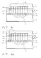
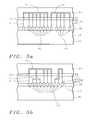
- FIG. 3 ais a representation of a silicon substrate over which an interconnect network is created according to the invention. Power and/or ground pads are provided for external connection.
- the chip structure that is shown in FIGS. 3 a and 3 brelates to power and ground distribution networks of the invention.
- 66represents one or more than one layers of metal.
- FIG. 3 bfurther distributes the power and ground to the circuit nodes through power and ground distribution lines that are below a layer of passivation and power and ground distribution lines that are above a layer of passivation.
- 66 and 66 ′each represent one or more than one layer of metal.
- FIG. 3 cshows an alternative wherein contact is made to a conventional bond pad through the passivation layer rather than through a post-passivation thick wide metal system.
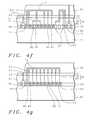
- FIG. 4 ais a representation of a silicon substrate over which an interconnect network is created according to the invention.
- An ESD and/or driver and/or receiver circuit access padis provided through the surface of the layer of dielectric for external connection.
- the chip structure that is shown in FIGS. 4 a and 4 baddresses clock and signal distribution networks of the invention. “Signals” refer to, but are not limited to, address and data. 72 in the figure represents one or more than one layer of metal.
- FIG. 4 bfurther distributes signal and clock to the circuit nodes through clock and signal distribution lines that are below a layer of passivation in addition to clock and signal distribution lines that are above a layer of passivation.
- 71 and 71 ′each represent one or more than one layers of metal.
- FIGS. 4 c and 4 dshow smaller intra-chip circuit drivers.
- FIGS. 4 e through 4 hshow an alternative for the embodiments in FIGS. 4 a to 4 d, respectively, wherein contact is made to a conventional bond pad through the passivation layer rather than through a post-passivation thick wide metal system.
- FIG. 4 ishows two drivers, receivers or I/O circuits sharing a common ESD circuit by using the post-passivation interconnect to connect the drivers, receivers or I/O circuits to the common ESD circuit.
- FIG. 4 jshows multiple (more than two) drivers, receivers, and/or I/O circuits connected to multiple ESD circuits (more than one) using low-impedance post-passivation interconnects.
- FIG. 5 ais a representation of a silicon substrate over which an interconnect network is created according to the invention. No I/O connect pad is provided for external connection in specific networks.
- the chip structure that is shown in FIGS. 5 a and 5 baddresses clock and signal distribution networks of the invention.
- FIG. 5 bdifferentiates between clock and signal distribution lines that are below a layer of passivation and clock and signal distribution lines that are above a layer of passivation.
- FIGS. 5 c and 5 dshow smaller intra-chip circuit drivers.
- FIG. 5 eshows a series of driver/receivers, or transceivers, or repeater devices using the post-passivation interconnects of the present invention.
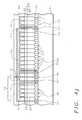
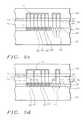
- FIGS. 6 a and 6 bare cross-sections of the interconnect structure of the present invention including contact pads on top of the post-passivation interconnection structure for connection to external circuits through wirebonds, gold bumps and solder bumps.
- FIGS. 6 c and 6 dare cross-sections of the interconnect structure of the present invention including contact made to a conventional bond pad through the passivation layer rather than through a post-passivation thick wide metal system for connection to external circuits through wirebonds, gold bumps and solder bumps.
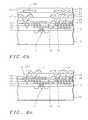
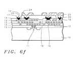
- FIG. 6 eshows details of metal structure in each layer of post-passivation interconnection structure.
- FIG. 6 fis a cross section similar to FIG. 6 c except that a metal cap is formed in the passivation openings.
- the metal capis formed by aluminum or gold to protect the damascene copper used in the fine line metal scheme.
- U.S. Pat. No. 6,383,916to a common inventor as the current invention, teaches an Integrated Circuit structure where re-distribution and interconnect metal layers are created in layers of dielectric over the passivation layer of a conventional Integrated Circuit (IC).
- ICIntegrated Circuit
- a layer of passivationis deposited over the IC, a thick layer of polymer is alternately deposited over the surface of the layer of passivation, and thick, wide metal lines are formed over the passivation.
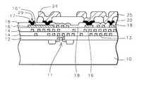
- FIG. 6 athere is shown a cross section of one implementation of U.S. Pat. No. 6,383,916.
- the surface of silicon substrate 10has been provided with transistors 11 and other devices (not shown in FIG. 6 a ).
- the surface of substrate 10is covered by an interlevel dielectric (ILD) layer 12 , formed over the devices.
- ILDinterlevel dielectric
- Layers 14represent all of the metal layers and dielectric layers that are typically created on the dielectric layer 12 .
- Layers 14contain multiple layers of dielectric or insulation and the like.
- Conductive interconnect lines 13make up the network of electrical connections that are created throughout layers 14 .
- Overlying and on the surface of layers 14are points 16 of electrical contact. These points 16 of electrical contact can, for instance, be bond pads that establish electrical interconnects to external circuits. These points of contact 16 can be points of interconnect within the IC arrangement that establish electrical interconnects to the transistors and other devices in the surface of the substrate. These metal layers are referred to as fine line metal interconnections.
- the intermetal dielectric (IMD) layerscomprise silicon-based oxides, such as silicon dioxide formed by a chemical vapor deposition (CVD) process, CVD TEOS oxide, spin-on-glass (SOG), fluorosilicate glass (FSG), high density plasma CVD oxides, or the composite layer formed by a portion of this group of materials.
- the IMD layerstypically have a thickness of between about 1000 and 10,000 Angstroms.
- the fine line metal interconnectionsare typically formed by sputtering aluminum or an aluminum alloy and patterning the aluminum to form the fine metal lines. Alternatively, the fine lines may be formed by a copper damascene process.
- the copperis protected by an adhesion/barrier layer not only underlying the copper, but also surrounding the copper at the sidewalls of the line through the IMD.
- These fine linestypically have a thickness of between about 1000 and 10,000 Angstroms.
- a typical clean room environment of class 10 or lessis required; that is, having no more than 10 particles larger than 0.5 microns in any given cubic foot of air.
- the clean room environment of class 1 or even betteris required.
- the fine line IC metalis fabricated using 5 ⁇ steppers or scanners or better and using a photoresist layer having thickness of less than 5 microns.
- a passivation layer 18formed of, for example, a composite layer of silicon oxide and silicon nitride or oxynitride (the thickness of silicon nitride or oxynitride is usually thicker than about 0.3 ⁇ m for the passivation purpose), is deposited over the surface of layers 14 , and functions to prevent the penetration of mobile ions (such as sodium ions), moisture, transition metals (such as gold, copper, silver), and other contamination.
- the passivation layeris used to protect the underlying devices (such as transistors, polysilicon resistors, poly-to-poly capacitors, etc.) and the fine-line metal interconnection.
- metallizationis performed to create thick, wide metal lines 24 and 25 and to connect to contact points 16 .
- Lines 24 and 25can be of any design in width and thickness to accommodate specific circuit design requirements.
- the thick, wide metal of the post passivation metal lines of the inventionis thicker then the typical fine-line metal layers by a ratio of between about 2 and 1000 times.
- the thick, wide metal linesare wider than the fine-line metal by a ratio of between about 2 and 1000 times.
- the thick, wide metal lineshave a thickness of between about 2 and 100 ⁇ m, and a width of greater than or equal to about 2 ⁇ m. Line spacing preferably is greater than or equal to about 2 ⁇ m.
- Thick, wide metal 25has smaller resistance and capacitance than the fine line metal 14 and is also easier and more cost effective to manufacture.
- the thick, wide metals linesare formed by a selective deposition process—by photoresist defined electroplating of metals. Gold and copper are preferred. Silver, palladium, and nickel are other possible choices.
- a top layer of polymer(not shown in FIG. 6 a ) can also be formed to encapsulate the thick, wide metal 25 .
- the clean room environment of the post-passivation metal processcan be of a class 100 or more; that is, having 100 or more particles larger than 0.5 microns in any given cubic foot of air.
- a clean room environment of class 10may be required.
- aligners or 1 ⁇ steppersare used with a photoresist having a thickness of greater than about 5 microns.
- the thick, wide metal lineshave a thickness of between about 2 and 100 microns and a width of larger than about 2 microns.
- An advantage of the selective deposition process of the inventionis a minimization of wasted material, especially when precious metal, such as gold, silver, or palladium is used.
- precious metalsuch as gold, silver, or palladium
- the metalis electroplated only where it is needed.
- metal damascene process used for fine line metallizationmetal is electroplated everywhere and then etched or polished away where it is not needed. Covering the whole wafer with thick metal creates stress which causes the process problem. This is a waste of metal, especially for the cases when precious metal is used. The removed metal is often contaminated and may not be able to be reused or may be very expensive to be reused.
- the thickness of selective electroplated metalis defined by the thickness of photoresist, which can be formed as thick as 100 microns.
- the thickness of photoresistwhich can be formed as thick as 100 microns.
- a primary limitation to forming thick copper damascene linesis the thickness of the chemical vapor deposited (CVD) oxides which define the damascene copper thickness. CVD oxides cannot be thickly deposited due to stress concerns. It is also very expensive to deposit thick CVD oxides.
- the photoresistis removed.
- the adhesion/barrier layer 22comprising TiW, TaN, Cr, Ti, or TiN
- seed layer 23comprising the same metal as the electroplated metal
- the adhesion/barrier layer 22is removed by etching using the electroplated metal layer 24 as a mask.
- an undercut 21is formed in the adhesion/barrier layer 22 , as shown in FIG. 6 e.
- the undercutis usually between about 0.03 to 2.0 micron per side, depending on etching recipe and over-etch time.
- the chip structure of the thick, wide post-passivation metal 24 and 25is different from the chip structure of the fine line metallization.
- the undercut 21 in the adhesion/barrier layerthere is a clear boundary between the sputtered seed layer 23 and the electroplated metal 24 and 25 . This can be seen, for example, in a transmission electron microscope (TEM) image.
- TEMtransmission electron microscope
- the entire metal bodyis constructed by two layers of materials having the same constitution (i.e. gold copper, silver, palladium, or nickel), but different microstructure.
- the grain size of the electroplated metalis much larger than that of the seed layer, by at least two times.
- the grain size of the sputtered gold layeris about 1,000 Angstroms, and the grain boundary is perpendicular to the surface of substrate.
- the grain size of the electroplated goldis greater than about 2 microns with the grain boundary not perpendicular, and typically, at an angle of about 45 degrees from the substrate surface. In the fine line metal interconnections, there is no undercutting or clear boundary of grain size difference inside the aluminum layer.
- the fine line metal linescan be copper damascene lines. Even if the post-passivation metal is also copper, the chip structure of the post-passivation metal lines is still different from the fine line metal lines. As described above, an undercut in the adhesion/barrier layer is formed during etching of that layer in the post-passivation metal process. Additionally, the adhesion/barrier layer 22 in the post-passivation metal structure is formed only under the copper line, as shown in FIG. 6 e. In the copper damascene process of the fine line metallization, an adhesion/barrier layer is needed not only at the bottom, but also at the sidewalls of the copper line. This is needed primarily to protect the underlying active devices from copper ions. However, in the post-passivation scheme of the invention, the passivation layer 18 provides the barrier to copper ions.
- a second layer of polymer 21is deposited and patterned, followed by the formation of the second layer of thick, wide metal 26 , 27 by selective deposition.
- a final encapsulation 22covers the whole wafer with some exposed pads 28 for connection to external circuits. The exposed pads 28 are connected to external circuits through solder bumps, gold bumps, and/or wirebonds.
- FIGS. 6 c and 6 dare analogous to FIGS. 6 a and 6 b, respectively, but show the process of the invention in conjunction with exposed pads on the top layer of the fine line metal structure for connection to the external circuits. Openings 29 have been made to aluminum pad 16 .
- Conventional wirebonding techniquesmay be used to form wirebond connections to the original Aluminum pad 16 exposed by openings 29 in FIGS. 6 c and 6 d.
- a piece of aluminum 16 ′′is used for a short distance interconnection between wirebonding pads and the post-passivation interconnection.
- gold bump or solder bump connectionmay be used to connect contact pads 16 ′ to external circuits.
- fine line metal 13is formed by the damascene copper, as shown in FIG.
- a metal cap 17is formed in the openings 29 .
- the metal capis formed by either aluminum or gold.
- a piece of damascene copper 16 ′′is used for a short distance interconnection between contact pads 16 ′ and the post-passivation interconnection 24 .
- the following commentsrelate to the size and the number of the contact points 16 in FIGS. 6 a - 6 d. Because these contact points 16 are located on top of a thin dielectric (layer 14 , FIGS. 6 a - 6 d ) the pad size cannot be too large since a large pad size brings with it a large capacitance. In addition, a large pad size will interfere with the routing capability of that layer of metal. It is therefore preferred to keep the size of the pad 16 relatively small.
- the size of the contact pad 16can be in the order of 0.5 ⁇ m to 40 ⁇ m, the exact size being dependent on the electrical requirements of the contacts.
- Layer 18 in FIGS. 6 a - 6 dcan be a typical IC passivation layer.
- the most frequently used passivation layer in the present state of the artis plasma enhanced CVD (PECVD) oxide and nitride.
- PECVDplasma enhanced CVD
- a layer of approximately 0.5 ⁇ m PECVD oxidecan be deposited first followed by a layer of approximately thicker than about 0.3 ⁇ m nitride.
- Passivation layer 18is very important because it protects the device wafer from moisture and foreign ion contamination.
- the silicon nitrideis usually thicker than about 0.3 ⁇ m.
- this layerbetween the sub-micron process (of the integrated circuit) and the tens-micron process (of the post-passivation metallization structure) is of critical importance since it allows for a cheaper process that has less stringent clean room requirements for the process of creating the interconnecting metallization structure.
- Layers 20 , 21 ,and 22are thick polymer dielectric layers (for example polyimide) that have a thickness in excess of 2 ⁇ m (after curing).
- the range of the polymer thicknesscan vary from 2 ⁇ m to 150 ⁇ m, dependent on electrical design requirements.
- a polymercan be spin-on coated and cured. After spin-on coating, the polymer will be cured at 370 degrees C. for 1 hour in a vacuum or nitrogen ambient. For a thicker polymer, the polymer film can be multiple coated and cured. The polymer also can be formed by screen printing.
- a polymer such as a polyimidecan be used as the polymer.
- Another material that can be used to create layers 20 , 21 , 22is the polymer benzocyclobutene (BCB) (Dow Chemical Company, Midland, Mich.), which has recently gained acceptance to be used instead of typical polyimide application.
- Other possible materials for layers 20 , 21 , 22include a silicone elastomer, or parylene.
- the epoxy-based materialsuch as photoepoxy SU-8 (Sotec Microsystems, Renens, Switzerland) can also be used.
- the thick layers 20 , 21 , 22 of polymercan be coated in liquid form on the surface of the layer 18 of passivation or it can be laminated over the surface of the layer 18 of passivation in dry film form.
- the intermetal polymer layermay require a planarization process.
- the polymer layerscan be planarized by the chemical-mechanical polishing (CMP). Planarization can be immediately after depositing each intermetal polymer layer or before forming each layer of post-passivation metallization and after forming openings in the intermetal polymer layer.
- CMPchemical-mechanical polishing
- Additional electrical componentssuch as an inductor, a capacitor, and the like, not shown, can be created on the surface of layer 20 or 22 of polyimide and in electrical contact with underlying metallization.
- FIG. 3 athis figure refers to power and ground architecture.
- FIG. 3 aa silicon substrate 40 over which an interconnect network 60 is created according to the invention, with a wide and thick post-passivation wire interconnect network 66 created in a thick layer 64 of dielectric overlying a layer 62 of passivation.
- a power and/or ground padcan be provided for external connection.
- FIG. 3 acan be summarized as follows: a silicon substrate 40 is provided in the surface of which have been created semiconductor devices 42 and at least one electrostatic discharge (ESD) circuit 44 ; one or more layers 60 ′′ of dielectric are deposited over the substrate 40 ; a fine-line interconnect network 60 is created in the dielectric layers 60 ′′ making contact with the active circuits 42 and the ESD circuit 44 . A layer 62 of passivation is deposited over the fine-line interconnect network 60 . Openings 63 are created in the layer 62 of passivation that aligns with points of contact in the top layer of the fine-line interconnect network 60 .
- ESDelectrostatic discharge
- a thick layer of dielectricis optionally deposited over the layer 62 of passivation.
- An adhesion/barrier layer and a seed layerare deposited over the whole substrate 40 .
- a thick photoresist layeris deposited to a thickness greater than the desired bulk metal thickness.
- Conventional lithographyis used to expose the seed layer in those areas where electroplating thick, wide metallization 66 is desired.
- a wide thick line post-passivation interconnect network 66is created by selective deposition in the layer of dielectric 64 , contacting the ESD circuits 44 and the internal circuits 42 .
- a point of electrical contactcomprising a power or ground contact 68 , 68 ′ is provided in the surface of the thick layer 64 of dielectric.
- a selective deposition processforms the post-passivation metal lines 66 .
- An advantage of the selective deposition process of the inventionis a minimization of wasted material, especially when precious metal, such as gold, silver, or palladium is used.
- precious metalsuch as gold, silver, or palladium
- the metalis electroplated only where it is needed.
- metal damascene process used for fine line metallizationmetal is electroplated everywhere and then etched or polished away where it is not needed. This is a waste of expensive metal especially for the cases when precious metal, is used. The removed metal is often contaminated and may not be able to be reused or may be very expensive to be reused.
- FIG. 3 bprovides further insight into the creation of the power and ground post-passivation interconnect lines of the invention whereby these interconnect lines have been shown as thick, wide interconnect lines 66 and fine line interconnect lines 66 ′.
- Post-passivation thick interconnect lines 66have been created above the layer 62 of passivation and act as global power and ground interconnect lines.
- Fine line interconnect lines 66 ′have been created below the layer 62 of passivation and act as local power and ground interconnect lines.
- thick, wide interconnect line 66represents the combined (for multiple connection scheme in layer 64 ) power or ground bus or plane. This could be one or more than one thick, wide post-passivation metal layers 66 as well as intervening dielectric including a polymer.
- Metal scheme 66 ′represents the combined (for multiple connection scheme in layer 60 ′′ of dielectric) power or ground bus or plane. This could be one or more than one fine-line metal layers 66 ′ as well as intervening dielectric usually including a silicon-based oxide.
- the fine-line metal layers 66 ′are connected through openings in the silicon-based inter-metal dielectrics. Alternately, if the current is large, wide metal lines 66 can be used in the fine-line interconnect network 60 .
- FIG. 3 cprovides an alternative in which contact is made to conventional aluminum metal layers 61 ′, for example, through the passivation layer 62 rather than making contact to the post-passivation thick, wide metal system 66 .
- the top layer of metal layers 61 ′is used for contact pad purposes and for connection between the contact pad 58 ′ and the wide, thick interconnect lines 66 .
- the distance of metal layers 61 ′is a short distance; for example, ⁇ 500 ⁇ m in length.
- the contact pad 58 ′can then be connected to external circuits through wirebonds, gold bumps and/or solder bumps.
- the post passivation metallizationcan optionally be performed directly on the passivation layer 62 without the intervening polymer insulating layer.
- the insulating polymer layerprovides distinct advantages, it may be desirable to remove the insulating polymer layer in order to save costs.
- FIG. 4 aaddresses the interconnections of signal and clock line.
- Signalhere includes address, data, logic, and analog signals.
- Signalalso includes the power/ground voltage output from voltage regulators.
- FIG. 4 athere is shown a cross section of a silicon substrate 40 over which an interconnect network is created according to the invention.
- An access pad 70 to an ESD circuit 44 or driver or receiver circuits or I/O circuits 45 ′is provided through the surface of the layer 64 of dielectric for external connection.
- the I/O interconnectcan also be provided to a receiver circuit or a driver circuit or an I/O circuit 45 ′.
- the method that is used to create the interconnect network 72 that is shown in cross section in FIG. 4 acan be summarized as follows.
- a silicon substrate 40is provided; active circuits 42 have been created in the surface of the substrate 40 including an ESD circuit 44 , receiver, driver and I/O circuit 45 ′.
- First layers 58 of dielectric of inorganic materialare deposited over the substrate 40 and a fine-line interconnect network 60 ′ is created in the layers 60 ′′ of dielectric, making contact with the active circuitry.
- a layer 62 of passivationis deposited over the first thin layers 60 ′′ of dielectric; openings 63 are made through the passivation layer 62 to align with points of electrical contact in the surface of the first layers 60 ′′ of dielectric.
- One or more thicker layers 64 of dielectricare deposited over the surface of the layer 62 of passivation, typically of an organic material; a wide thick line post-passivation interconnect network 72 is created in the thicker layer 64 of dielectric by selective deposition, making electrical contact with the metal pads under the layer 62 of passivation, including to the one ESD circuit 44 , receiver, driver or I/O circuit 45 ′. A point of electrical contact is provided in the surface of the second layer of dielectric to the ESD circuit 44 , receiver, driver or I/O circuit 45 ′.
- FIG. 4 bprovides further insight into the creation of the signal and clock post-passivation interconnect lines of the invention whereby these interconnect lines have been shown as thick, wide interconnect lines 71 and fine-line interconnect lines 71 ′.
- Post-passivation interconnect lines 71have been created above the layer 62 of passivation and act as global signal and clock interconnect lines.
- Fine line interconnect lines 71 ′have been created below the layer 62 of passivation and act as local signal and clock interconnect lines.
- internal circuits 42have no driver, no receiver, and no ESD connections.
- Intra-chip drivers and receiversmay be necessary if the interconnection distance is long and/or the load of the net of circuits is large.
- a driver circuitis used to drive a load; i.e., to charge up the capacitance of a net formed with circuits and interconnects by the drive current.
- a driver currentis the output of a driver circuit.
- the ability to drive currentis proportional, in CMOS devices, to the W/L ratio, where W/L is the ratio of the device channel width to its length.
- These intra-chip driversare typically smaller than off-chip I/O drivers. For the ability to detect a signal level, the sensitivity of a receiver is dependent on the sensing amplifier, or latched input circuits, or cascade stages.
- Intra-chip drivers and receivers 80are shown in FIGS. 4 c and 4 d.
- Intra-chip circuits 80typically have no ESD circuits and no I/O circuits. For short distance on-chip interconnection, no intra-chip circuits may be required.
- FIG. 4 dshows an example of internal circuits 42 that need to utilize attached intra-chip drivers or receivers 80 while internal circuits 42 ′ do not require attached intra-chip drivers or receivers 80 .
- Intra-chip circuitsare usually smaller than the off-chip drivers.
- the intra-chip driver circuitsare different from the off-chip circuits in that they have no I/O circuits and no ESD circuits.
- FIGS. 4 c and 4 dshow smaller internal driver circuits 80 connected to the internal circuits 42 .
- Driver/receiver/I/O circuits 45 ′are larger than off-chip circuits.
- connection to external circuitsis made through pad 70 formed and exposed on the top of the post-passivation metal structure.
- the connection to external circuitscan be made through solder bumps, gold bumps and/or wirebonds.
- the connection to external circuitscan be made on a conventional aluminum metal 70 ′, for example, through the passivation layer 62 rather than making contact to the post-passivation thick, wide metal system.
- FIGS. 4 e, 4 f, 4 g, and 4 hdescribe the similar design architecture as in FIGS. 4 a, 4 b, 4 c, and 4 d, respectively, except that pads for connection to external circuits are at different structure levels.
- FIG. 4 ishows two drivers, receivers or I/O circuits 45 sharing a common ESD circuit 44 by using the post-passivation interconnect 72 ′ to connect the drivers, receivers or I/O circuits 45 to the common ESD circuit 44 .
- Each driver, receiver or I/O circuit 45is connected to the internal circuits 42 through the post-passivation interconnects 72 .
- the drivers, receivers, or I/O circuits 45 and the ESD circuit 44are connected to the external circuits at the contact point 70 .
- Multiple (more than two) drivers, receivers, and/or I/O circuits 45can be connected to multiple ESD circuits 44 (more than one) using the post-passivation interconnects 72 ′.
- FIG. 4 ishows two drivers, receivers or I/O circuits 45 sharing a common ESD circuit 44 by using the post-passivation interconnect 72 ′ to connect the drivers, receivers or I/O circuits 45 to the common ESD circuit 44 .
- FIG. 5 ashows a representation of a silicon substrate 40 over which an interconnect network is created according to the invention, with the post-passivation interconnect network created in a thick layer 64 of dielectric overlying a layer 62 of passivation and remaining internal to the thick layer 64 of dielectric. No ESD, receiver, driver or I/O circuit access pad is provided for external connection to the internal circuits 42 . Shown in FIG. 5 a and not previously highlighted is the clock or signal post-passivation interconnect line 74 , providing for an interconnect scheme of thick, wide lines overlying a passivation layer 62 whereby no external I/O connections are provided.
- each thick, wide interconnect line 74(where such thick, wide interconnect lines are used) must be provided with at least one I/O connect point for off-chip connection.
- the method that is used to create the wide thick line post-passivation interconnect lines that is shown in cross section in FIG. 5 acan be summarized as follows and is similar to that described above for FIG. 4 a.
- a silicon substrate 40is provided. Active devices 42 have been provided in and/or on the surface of the substrate 40 .
- First thin layers of dielectric 58are deposited over the surface of the substrate 40 , a fine-line interconnect network 60 is created in the first layers of dielectric comprising fine-line interconnect lines 60 ′, making contact with points of electrical contact in the surface of the substrate 40 .
- a layer 62 of passivationis deposited over the surface of the first layers 60 ′′ of dielectric.
- Second thick layers 64 of dielectricare deposited over the surface of the passivation layer 62 , a post-passivation interconnect network is created in the second layers 64 of dielectric comprising thick, wide interconnect lines 74 , created by selective deposition, making contact with points 63 of electrical contact in the passivation layer 62 .
- FIG. 5 bprovides further insight into the creation of the signal and clock interconnect lines of the invention whereby these interconnect lines have been shown as post-passivation interconnect lines 71 and fine line interconnect lines 71 ′.
- Post-passivation interconnect lines 71have been created above the layer 62 of passivation and can act as global signal and clock interconnect lines.
- Fine line interconnect lines 71 ′have been created below the layer 62 of passivation and act as local signal and clock interconnect lines 71 ′.
- internal circuits 42are shown. Circuits 42 have no I/O circuits and no ESD circuits.
- FIGS. 5 c and 5 dshow smaller internal driver circuits 80 connected to the internal circuits 42 ′, while no smaller internal drivers are connected to the internal circuits 42 .
- FIG. 5 eshows a series of driver/receivers, 101 ′ 102 ′ or transceivers, 103 or repeater 103 devices.
- An internal circuit 42is connected to an internal circuit 42 ′ at a distance.
- a series of repeaters or transceivers 103 together with the post-passivation interconnects 74are applied.
- a repeater or transceiver 103consists typically of a receiver 102 ′ and a driver 101 ′, using fine-line connection 103 ′′ in series.
- the circuit 42uses fine-line connection 101 ′′ to connect to an on-chip driver 101 , driving through post-passivation interconnects 74 , and passing repeaters 103 , and arriving at the receiver 102 and the internal circuit 42 ′.
- the repeaters or transceivers combined with the post-passivation interconnectsprovide methods for interconnecting different functions on a system-on-a-chip (SOC) chip.
- FIGS. 3-5show a fine-line interconnect network 60 that underlies the layer 62 of passivation
- the inventionalso enables and can be further extended with the complete elimination of the fine-line interconnect network 60 and creating an post-passivation interconnect network 66 , 71 , 72 , 72 , 72 ′, 73 , 74 that uses only thick, wide wires.
- the first layer 60 ′′ of dielectricis not applied and the layer 62 of passivation is deposited directly over the surface of the created semiconductor devices 42 in or on the surface of substrate 40 .
- the post-passivation interconnection lines of the present inventionare formed of thick, wide metal layers, the thickness reducing resistance. Use of the intermetal polymer dielectric between metal layers reduces capacitance. With the reduced capacitance, a higher frequency of operation results due to a higher resonant frequency.
- Metal capacitanceincludes three components: 1) plate capacitance which is a function of the metal width to dielectric thickness aspect ratio, 2) coupling capacitance which is a function of the metal thickness to line spacing aspect ratio, and 3) fringing capacitance which is a function of metal thickness, spacing, and dielectric thickness.
- fine line metal thicknessis about 2 ⁇ m
- fine line metal widthis about 10 ⁇ m
- fine line IMD thicknessis about 2 ⁇ m
- the line spacingis about 10 ⁇ m.
- Post-passivation metal thicknessis about 5 ⁇ m
- metal widthis about 10 ⁇ m
- dielectric thicknessis about 5 ⁇ m
- lines spacingis also about 10 ⁇ m.
- the metal thickness differenceresults in a 2.5 times reduction in resistance (per unit length) in the post-passivation metal structure over the fine line metal structure.
- the dielectric thicknessresults in a 2.5 times difference in capacitance (per unit length) in the post-passivation metal structure over the fine line metal structure.
- the reduction in resistance (per unit length) times capacitance (per unit length)is 6.25 times, or about 5 times.
- fine line metal thicknessis about 1 ⁇
- fine line metal widthis about 10 ⁇ m
- fine line IMD thicknessis about 0.5 ⁇ m
- the line spacingis about 2 ⁇ m.
- Post-passivation metal thicknessis about 5 ⁇ m
- metal widthis about 10 ⁇ m
- dielectric thicknessis about 5 ⁇ m
- lines spacingis about 10 ⁇ m.
- the metal thickness differenceresults in about a 5 times reduction in resistance (per unit length) in the post-passivation metal structure over the fine line metal structure.
- the capacitance (per unit length)is dominated in this case by plate capacitance with a reduction of 10 times difference in capacitance (per unit length) in the post-passivation metal structure over the fine line metal structure.
- the reduction in RC productis about 50 times.
- typical capability fine line metal thicknessis about 0.4 ⁇ m
- fine line metal widthis about 0.2 ⁇ m
- fine line IMD thicknessis about 0.4 ⁇ m
- the line spacingis about 0.2 ⁇ m.
- Post-passivation metal thicknessis about 5 ⁇ m
- metal widthis about 10 ⁇ m
- dielectric thicknessis about 5 ⁇ m
- line spacingis about 10 ⁇ m.
- the metal thickness differenceresults in about a 625 times reduction in resistance (per unit length) in the post-passivation metal structure over the fine line metal structure.
- the capacitance (per unit length)is dominated by coupling capacitance and results in about a 4 times difference in capacitance (per unit length) in the post-passivation metal structure over the fine line metal structure.
- the reduction in RC productis about 2,500 times.
- typical capability fine line metal thicknessis about 0.4 ⁇ m
- fine line metal widthis about 0.2 ⁇ m
- fine line IMD thicknessis about 0.4 ⁇ m
- the line spacingis about 0.2 ⁇ m.
- Post-passivation metal thicknessis about 10 ⁇ m
- metal widthis about 10 ⁇ m
- dielectric thicknessis about 10 ⁇ m
- line spacingis about 40 ⁇ m.
- the metal thickness differenceresults in about a 1250 times reduction in resistance (per unit length) in the post-passivation metal structure over the fine line metal structure.
- the capacitance (per unit length)is dominated by coupling capacitance and results in about an 8 times difference in capacitance (per unit length) in the post-passivation metal structure over the fine line metal structure.
- the reduction in RC productis about 10,000 times.
- the RC product (per unit length) of the post-passivation metal structurecan be about 5 to 10,000 times smaller than the RC product of the fine line metal structure.
- the post-passivation interconnection of the present inventioncan connect to three types of circuits (i) off-chip drivers, receivers, I/O circuits, and ESD circuits, (ii) intra-chip drivers and receivers, and (iii) internal circuits.
- No driveris required for freeway interconnection with a distance ⁇ “D”.
- a smaller driveris used for freeway interconnection with a distance >“D”; that is, intra-chip connection.
- a large driverlarger than the intra-chip driver, is used for off-chip connection.
Landscapes
- Physics & Mathematics (AREA)
- Condensed Matter Physics & Semiconductors (AREA)
- General Physics & Mathematics (AREA)
- Engineering & Computer Science (AREA)
- Computer Hardware Design (AREA)
- Microelectronics & Electronic Packaging (AREA)
- Power Engineering (AREA)
- Geometry (AREA)
- Internal Circuitry In Semiconductor Integrated Circuit Devices (AREA)
Abstract
Description
- This is a continuation application of application Ser. No. 10/962,963, filed on Oct. 12, 2004.
- This application is related to application Ser. No. 10/278,106, filed on Oct. 22, 2002, now U.S. Pat. No. 6,734,563, which is a division of application Ser. No. 09/691,497, filed on Oct. 18, 2000, now U.S. Pat. No. 6,495,442, all assigned to a common assignee and all herein incorporated by reference in their entirety.
- This application is also related to application Ser. No. 09/721,722, filed on Nov. 27, 2000, now U.S. Pat. No. 6,303,423, assigned to a common assignee and herein incorporated by reference in its entirety.
- (1) Field of the Invention
- The invention relates to the fabrication of integrated circuit devices, and more particularly, to a method of post-passivation processing for the creation of conductive interconnects.
- (2) Description of the Related Art
- Improvements in semiconductor device performance are typically obtained by scaling down the geometric dimensions of Integrated Circuits; this results in a decrease in the cost per die while at the same time some aspects of semiconductor device performance are improved. The metal connections which connect the Integrated Circuit to other circuit or system components become of relative more importance and have, with the further miniaturization of the IC, an increasingly negative impact on the circuit performance. The capacitance and resistance of the metal interconnections increase, which degrades the chip performance significantly. Of most concern in this respect is the voltage drop along the power and ground buses and the RC delay of the critical signal paths. Attempts to reduce the resistance by using wider metal lines result in higher capacitance of these wires.
- To solve this problem, one approach has been to develop low resistance metal (such as copper) for the wires while low-k dielectric materials are used in between signal lines. Current practice is to create metal interconnection networks under a layer of passivation. This approach, however, limits the interconnect network to fine line interconnects and the therewith associated high line capacitance and high line resistance. The latter two parameters, because of their relatively high values, degrade circuit performance, an effect which becomes even more severe for higher frequency applications and for long interconnect lines that are, for instance, used for clock distribution lines. Also, fine line interconnect metal cannot carry high values of current that is typically needed for ground busses and for power busses.
- From the aspect of IC metal interconnection history, sputtered aluminum has been a mainstream IC interconnection metal material since the 1960's. The aluminum film is sputtered to cover the whole wafer, and then the metal is patterned using photolithography methods and dry and/or wet etching. It is technically difficult and economically expensive to create thicker than 2 μm aluminum metal lines due to the cost and stress concerns of blanket sputtering. About 1995, damascene copper metal became an alternative for IC metal interconnection. In damascene copper, the insulator is patterned and copper metal lines are formed within the insulator openings by blanket electroplating copper and chemical mechanical polishing (CMP) to remove the unwanted copper. Electroplating the whole wafer with thick metal creates large stress. Furthermore, the thickness of damascene copper is usually defined by the insulator thickness, typically chemical vapor deposited (CVD) oxides, which does not offer the desired thickness due to stress and cost concerns. Again it is also technically difficult and economically expensive to create thicker than 2 μm copper lines.
- It has previously been stated that it is of interest to the semiconductor art to provide a method of creating interconnect lines that removes typical limitations that are imposed on the interconnect wires, such as unwanted parasitic capacitances and high interconnect line resistance. U.S. Pat. No. 6,383,916 to the same inventor as the present invention provides such a method. An analogy can be drawn in this respect whereby the currently (prior art) used fine-line interconnection schemes, which are created under a layer of passivation and providing high density interconnects, are the streets in a city; in the post-passivation interconnection scheme of the above patent, the interconnections that are created above a layer of passivation and providing high performance interconnects can be considered the freeways between cities.
FIG. 1 shows a diagram of a silicon substrate on the surface of which has been created a conductive interconnect network. The chip structure that is shown inFIG. 1 addresses prior art power and ground distribution networks. The various features that have been highlighted inFIG. 1 are the following:- 40, a silicon substrate on the surface of which has been created an interconnect network
- 42, a sample number of semiconductor circuits that have been created in or on the surface of the
substrate 40 - 44, two electrostatic discharge (ESD) circuits created in or on the surface of the
substrate 40; one ESD circuit is provided for each pad that is accessible for external connections (pads 52, see below) - 46 is a layer of interconnect lines; these interconnect lines are above the surface of
substrate 40 and under thelayer 48 of passivation and represent a typical application of prior art fine-line interconnects; these fine-line interconnects oflayer 46 typically have high resistance and high capacitance. - 48 is a layer of passivation that is deposited over the surface of the
layer 46 of interconnect lines. The passivation layer is the final layer of the IC process in the prior art. The passivation layer is used to protect the underlying devices and fine-line interconnection from damage by mobile ions, moisture, transition metals, and contamination. - 50 is a power or ground bus that connects to the
circuits 42 via fine-line interconnect lines provided inlayer 46; this power or ground bus is typically of wider metal since this power or ground bus carries the accumulated current or ground connection for thedevices 42. The power or ground buses are built in the fine line interconnect under the passivation layer. The fine line interconnection can be in one layer or more than one layer of metals. - 52 is a power or ground pad that passes through the
layer 48 of passivation and that has been connected to the power orground bus 50.
- From the above the following can be summarized: circuits are created in or on the surface of a silicon substrate, interconnect lines are created for these circuits for further interconnection to external circuitry, the circuits are, on a per I/O pad basis, provided with an ESD circuit; these circuits with their ESD circuit are connected to a power or ground pad that penetrates a layer of passivation. The layer of passivation is the final layer that overlies the created interconnect line structure; the interconnect lines underneath the layer of passivation are fine line interconnects and have all the electrical disadvantages of fine line interconnects such as high resistance and high capacitance.
- Relating to the diagram that is shown in
FIG. 1 , the following comment applies: ESD circuits are, as is known in the art, provided for the protection of semiconductor circuits against unwanted electrostatic discharge. For this reason, each pad that connects a semiconductor circuit to the external circuits must be provided with an ESD circuit. FIG. 2 shows a diagram of a prior art configuration that resembles the diagram shown inFIG. 1 . The chip structure that is shown inFIG. 2 however relates to clock and signal distribution networks.FIG. 2 shows in addition (to the previously highlighted aspects ofFIG. 1 ):- 45 are two ESD circuits that are provided in or on the surface of the
substrate 40; ESD circuits are always required for any external connection to an input/output (I/O) pad. - 45′ which are circuits that can be receiver or driver or I/O circuits for input (receiver) or output (driver) or I/O purposes respectively.
- 54 is a clock, signal, address, or data bus built in the fine line interconnection metal under the passivation layer. The clock, signal, or buses can be in one layer or in more than one layer of fine line interconnect metals.
- 56 is a clock or signal pad that has been extended through the
layer 48 of passivation.
- 45 are two ESD circuits that are provided in or on the surface of the
- The same comments apply to the diagram that is shown in
FIG. 2 as previously have been made with respect toFIG. 1 , with as a summary statement that the layer of passivation is the final layer that overlies the created structure, the interconnect lines underneath the layer of passivation are fine line interconnects and have all the electrical disadvantages of fine line interconnects such as high resistance and high parasitic capacitance. - Further with respect to
FIG. 2 wherepads 56 are signal or clock pads: pads 56 must be connected to ESD and driver/receiver or I/O circuits 45- for signal or
clock pads 56, these pads must be connected not only to ESD circuits but also to driver or receiver or I/O circuits, highlighted ascircuit 45′ inFIG. 2 - after (clock and signal) stimuli have passed through the ESD and driver/receiver or I/O circuits, these stimuli are further routed using, under prior art methods, fine-line interconnect wires. A layer of passivation is deposited over the dielectric layer in which the interconnect network has been created.
- It is therefore of interest to the semiconductor art to provide a method of creating interconnect lines that removes typical limitations that are imposed on the interconnect wires, such as unwanted parasitic capacitances and high interconnect line resistance.
- A principal objective of the invention is to provide a method for the creation of post-passivation interconnect metal that allows for the use of thick and wide metal.
- Another objective of the invention is to create a new integrated circuit interconnection design architecture, analogous to the transportation networks, using the conventional IC fine-line interconnection under the passivation layer as the streets in the cities, and the newly created post-passivation interconnection above the passivation layer as the freeways between the cities.
- Another objective of the invention is to provide a method for the creation of post-passivation interconnect metal that uses the application of a thick layer of dielectric such as polymer.
- Another objective of the invention is to provide a method for the creation of post-passivation interconnect metal that uses the application of a thick layer of metal formed by selective electroplating.
- Yet another objective of the invention is to provide a method that allows for the creation of long post-passivation interconnect lines, whereby these long post-passivation interconnect lines do not have high resistance or introduce high capacitance.
- A still further objective of the invention is to create post-passivation interconnect lines that can carry high levels of current for the creation of power and ground distribution networks.
- A still further objective of the invention is to create post-passivation interconnect metal that can be created using cost effective methods of manufacturing by creating the interconnect metal on the surface of and after a layer of passivation has been deposited.
- In accordance with the objectives of the invention a new method is provided for the creation of post-passivation interconnect lines. Fine line interconnects are provided in a first layer of dielectric overlying semiconductor circuits that have been created in or on the surface of a substrate. A layer of passivation is deposited over the layer of dielectric; a thick second layer of dielectric is created over the surface of the layer of passivation. Thick and wide interconnect lines are created in the thick second layer of dielectric. Intra-chip drivers are connected to the thick, wide post-passivation interconnections.
FIG. 1 is a representation of a silicon substrate over which a prior art fine-line interconnect network is created over which a layer of passivation is deposited, and power and/or ground pads are provided through the layer of passivation for external connection. The chip structure that is shown inFIG. 1 addresses prior art power and ground distribution networks.FIG. 2 is a representation of a silicon substrate over which a prior art fine-line interconnect network is created over which a layer of passivation is deposited, and clock and/or signal pads are provided through the layer of passivation for external connection. The chip structure that is shown inFIG. 2 addresses prior art clock and signal distribution networks.FIG. 3 ais a representation of a silicon substrate over which an interconnect network is created according to the invention. Power and/or ground pads are provided for external connection. The chip structure that is shown inFIGS. 3 aand3brelates to power and ground distribution networks of the invention.66 represents one or more than one layers of metal.FIG. 3 bfurther distributes the power and ground to the circuit nodes through power and ground distribution lines that are below a layer of passivation and power and ground distribution lines that are above a layer of passivation.66 and66′ each represent one or more than one layer of metal.FIG. 3 cshows an alternative wherein contact is made to a conventional bond pad through the passivation layer rather than through a post-passivation thick wide metal system.FIG. 4 ais a representation of a silicon substrate over which an interconnect network is created according to the invention. An ESD and/or driver and/or receiver circuit access pad is provided through the surface of the layer of dielectric for external connection. The chip structure that is shown inFIGS. 4 aand4baddresses clock and signal distribution networks of the invention. “Signals” refer to, but are not limited to, address and data.72 in the figure represents one or more than one layer of metal.FIG. 4 bfurther distributes signal and clock to the circuit nodes through clock and signal distribution lines that are below a layer of passivation in addition to clock and signal distribution lines that are above a layer of passivation.71 and71′ each represent one or more than one layers of metal.FIGS. 4 cand4dshow smaller intra-chip circuit drivers.FIGS. 4 ethrough4hshow an alternative for the embodiments inFIGS. 4 ato4d,respectively, wherein contact is made to a conventional bond pad through the passivation layer rather than through a post-passivation thick wide metal system.FIG. 4 ishows two drivers, receivers or I/O circuits sharing a common ESD circuit by using the post-passivation interconnect to connect the drivers, receivers or I/O circuits to the common ESD circuit.FIG. 4 jshows multiple (more than two) drivers, receivers, and/or I/O circuits connected to multiple ESD circuits (more than one) using low-impedance post-passivation interconnects.FIG. 5 ais a representation of a silicon substrate over which an interconnect network is created according to the invention. No I/O connect pad is provided for external connection in specific networks. The chip structure that is shown inFIGS. 5 aand5baddresses clock and signal distribution networks of the invention.FIG. 5 bdifferentiates between clock and signal distribution lines that are below a layer of passivation and clock and signal distribution lines that are above a layer of passivation.FIGS. 5 cand5dshow smaller intra-chip circuit drivers.FIG. 5 eshows a series of driver/receivers, or transceivers, or repeater devices using the post-passivation interconnects of the present invention.FIGS. 6 aand6bare cross-sections of the interconnect structure of the present invention including contact pads on top of the post-passivation interconnection structure for connection to external circuits through wirebonds, gold bumps and solder bumps.FIGS. 6 cand6dare cross-sections of the interconnect structure of the present invention including contact made to a conventional bond pad through the passivation layer rather than through a post-passivation thick wide metal system for connection to external circuits through wirebonds, gold bumps and solder bumps.FIG. 6 eshows details of metal structure in each layer of post-passivation interconnection structure.FIG. 6 fis a cross section similar toFIG. 6 cexcept that a metal cap is formed in the passivation openings. The metal cap is formed by aluminum or gold to protect the damascene copper used in the fine line metal scheme.- U.S. Pat. No. 6,383,916, to a common inventor as the current invention, teaches an Integrated Circuit structure where re-distribution and interconnect metal layers are created in layers of dielectric over the passivation layer of a conventional Integrated Circuit (IC). A layer of passivation is deposited over the IC, a thick layer of polymer is alternately deposited over the surface of the layer of passivation, and thick, wide metal lines are formed over the passivation.
- Referring now more specifically to
FIG. 6 a,there is shown a cross section of one implementation of U.S. Pat. No. 6,383,916. The surface ofsilicon substrate 10 has been provided withtransistors 11 and other devices (not shown inFIG. 6 a). The surface ofsubstrate 10 is covered by an interlevel dielectric (ILD)layer 12, formed over the devices. - Layers14 (two examples are shown) represent all of the metal layers and dielectric layers that are typically created on the
dielectric layer 12.Layers 14 contain multiple layers of dielectric or insulation and the like.Conductive interconnect lines 13 make up the network of electrical connections that are created throughoutlayers 14. Overlying and on the surface oflayers 14 arepoints 16 of electrical contact. Thesepoints 16 of electrical contact can, for instance, be bond pads that establish electrical interconnects to external circuits. These points ofcontact 16 can be points of interconnect within the IC arrangement that establish electrical interconnects to the transistors and other devices in the surface of the substrate. These metal layers are referred to as fine line metal interconnections. - Typically, the intermetal dielectric (IMD) layers comprise silicon-based oxides, such as silicon dioxide formed by a chemical vapor deposition (CVD) process, CVD TEOS oxide, spin-on-glass (SOG), fluorosilicate glass (FSG), high density plasma CVD oxides, or the composite layer formed by a portion of this group of materials. The IMD layers typically have a thickness of between about 1000 and 10,000 Angstroms. The fine line metal interconnections are typically formed by sputtering aluminum or an aluminum alloy and patterning the aluminum to form the fine metal lines. Alternatively, the fine lines may be formed by a copper damascene process. In the copper damascene process, the copper is protected by an adhesion/barrier layer not only underlying the copper, but also surrounding the copper at the sidewalls of the line through the IMD. These fine lines typically have a thickness of between about 1000 and 10,000 Angstroms. In the fabrication process of the fine line metal interconnections, a typical clean room environment of
class 10 or less is required; that is, having no more than 10 particles larger than 0.5 microns in any given cubic foot of air. For the generation of the 0.2 μm CMOS technology or more advanced generations, the clean room environment ofclass 1 or even better is required. The fine line IC metal is fabricated using 5× steppers or scanners or better and using a photoresist layer having thickness of less than 5 microns. - A
passivation layer 18, formed of, for example, a composite layer of silicon oxide and silicon nitride or oxynitride (the thickness of silicon nitride or oxynitride is usually thicker than about 0.3 μm for the passivation purpose), is deposited over the surface oflayers 14, and functions to prevent the penetration of mobile ions (such as sodium ions), moisture, transition metals (such as gold, copper, silver), and other contamination. The passivation layer is used to protect the underlying devices (such as transistors, polysilicon resistors, poly-to-poly capacitors, etc.) and the fine-line metal interconnection. - The key steps of U.S. Pat. No. 6,383,916 begin with the deposition of a
thick layer 20 of an insulating polymer, preferably polyimide, which is deposited over the surface ofpassivation layer 18. Access must be provided to points ofelectrical contact 16; for this reason a pattern of openings is formed through thepolyimide layer 20 and thepassivation layer 18. Contact points16 are, by means of the openings that are created in thelayer 20 of polyimide, electrically extended to the surface oflayer 20. - After formation of the openings, metallization is performed to create thick,
wide metal lines Lines - Thick,
wide metal 25 has smaller resistance and capacitance than thefine line metal 14 and is also easier and more cost effective to manufacture. The thick, wide metals lines are formed by a selective deposition process—by photoresist defined electroplating of metals. Gold and copper are preferred. Silver, palladium, and nickel are other possible choices. Optionally, a top layer of polymer (not shown inFIG. 6 a) can also be formed to encapsulate the thick,wide metal 25. - In more detail, the clean room environment of the post-passivation metal process can be of a class 100 or more; that is, having 100 or more particles larger than 0.5 microns in any given cubic foot of air. For advanced applications, a clean room environment of
class 10 may be required. During photolithography in the post-passivation metal process, aligners or 1× steppers are used with a photoresist having a thickness of greater than about 5 microns. The thick, wide metal lines have a thickness of between about 2 and 100 microns and a width of larger than about 2 microns. - An advantage of the selective deposition process of the invention is a minimization of wasted material, especially when precious metal, such as gold, silver, or palladium is used. In the selective deposition process, the metal is electroplated only where it is needed. In contrast, in the standard metal damascene process used for fine line metallization, metal is electroplated everywhere and then etched or polished away where it is not needed. Covering the whole wafer with thick metal creates stress which causes the process problem. This is a waste of metal, especially for the cases when precious metal is used. The removed metal is often contaminated and may not be able to be reused or may be very expensive to be reused.
- Furthermore, in the selective deposition process of the invention, the thickness of selective electroplated metal is defined by the thickness of photoresist, which can be formed as thick as 100 microns. In other words, it is feasible and cost-effective to form thick metal by selective electroplating. By contrast, it is technically difficult to form thick metal by a damascene copper process. A primary limitation to forming thick copper damascene lines is the thickness of the chemical vapor deposited (CVD) oxides which define the damascene copper thickness. CVD oxides cannot be thickly deposited due to stress concerns. It is also very expensive to deposit thick CVD oxides.
- After electroplating, the photoresist is removed. As shown in an enlarged illustration in
FIG. 6 e,the adhesion/barrier layer 22, comprising TiW, TaN, Cr, Ti, or TiN, andseed layer 23, comprising the same metal as the electroplated metal, are removed by etching using the electroplatedmetal layer 24 as a mask. During the self-aligned wet etching of the adhesion/barrier layer, an undercut21 is formed in the adhesion/barrier layer 22, as shown inFIG. 6 e.The undercut is usually between about 0.03 to 2.0 micron per side, depending on etching recipe and over-etch time. - The chip structure of the thick, wide
post-passivation metal seed layer 23 and the electroplatedmetal - The fine line metal lines can be copper damascene lines. Even if the post-passivation metal is also copper, the chip structure of the post-passivation metal lines is still different from the fine line metal lines. As described above, an undercut in the adhesion/barrier layer is formed during etching of that layer in the post-passivation metal process. Additionally, the adhesion/
barrier layer 22 in the post-passivation metal structure is formed only under the copper line, as shown inFIG. 6 e.In the copper damascene process of the fine line metallization, an adhesion/barrier layer is needed not only at the bottom, but also at the sidewalls of the copper line. This is needed primarily to protect the underlying active devices from copper ions. However, in the post-passivation scheme of the invention, thepassivation layer 18 provides the barrier to copper ions. - Referring now to
FIG. 6 b,multiple layers of post-passivation metals can also be built for some applications. A second layer ofpolymer 21 is deposited and patterned, followed by the formation of the second layer of thick,wide metal final encapsulation 22 covers the whole wafer with some exposedpads 28 for connection to external circuits. The exposedpads 28 are connected to external circuits through solder bumps, gold bumps, and/or wirebonds. FIGS. 6 cand6dare analogous toFIGS. 6 aand6b,respectively, but show the process of the invention in conjunction with exposed pads on the top layer of the fine line metal structure for connection to the external circuits.Openings 29 have been made toaluminum pad 16. Conventional wirebonding techniques may be used to form wirebond connections to theoriginal Aluminum pad 16 exposed byopenings 29 inFIGS. 6 cand6d.Here, a piece ofaluminum 16″ is used for a short distance interconnection between wirebonding pads and the post-passivation interconnection. In some other applications, gold bump or solder bump connection may be used to connectcontact pads 16′ to external circuits. For the case whenfine line metal 13 is formed by the damascene copper, as shown inFIG. 6 f,ametal cap 17 is formed in theopenings 29. The metal cap is formed by either aluminum or gold. Here, a piece ofdamascene copper 16″ is used for a short distance interconnection betweencontact pads 16′ and thepost-passivation interconnection 24.- The following comments relate to the size and the number of the contact points16 in
FIGS. 6 a-6d.Because these contact points16 are located on top of a thin dielectric (layer 14,FIGS. 6 a-6d) the pad size cannot be too large since a large pad size brings with it a large capacitance. In addition, a large pad size will interfere with the routing capability of that layer of metal. It is therefore preferred to keep the size of thepad 16 relatively small. The size of thecontact pad 16 can be in the order of 0.5 μm to 40 μm, the exact size being dependent on the electrical requirements of the contacts. - The invention does not impose a limitation on the number of contact pads that can be included in the design; this number is not only dependent on package design requirements but is mostly dependent on the internal circuit design requirements.
Layer 18 inFIGS. 6 a-6dcan be a typical IC passivation layer. - The most frequently used passivation layer in the present state of the art is plasma enhanced CVD (PECVD) oxide and nitride. In creating
layer 18 of passivation, a layer of approximately 0.5 μm PECVD oxide can be deposited first followed by a layer of approximately thicker than about 0.3 μm nitride.Passivation layer 18 is very important because it protects the device wafer from moisture and foreign ion contamination. To achieve the passivation purpose, the silicon nitride is usually thicker than about 0.3 μm. The positioning of this layer between the sub-micron process (of the integrated circuit) and the tens-micron process (of the post-passivation metallization structure) is of critical importance since it allows for a cheaper process that has less stringent clean room requirements for the process of creating the interconnecting metallization structure. Layers - For the deposition of
layers - A polymer such as a polyimide (HD Microsystems, Parlin, N.J.) can be used as the polymer. Another material that can be used to create
layers layers - The thick layers20,21,22 of polymer can be coated in liquid form on the surface of the
layer 18 of passivation or it can be laminated over the surface of thelayer 18 of passivation in dry film form. - For the
thick layers - Additional electrical components such as an inductor, a capacitor, and the like, not shown, can be created on the surface of
layer - Now, the design architecture of the present invention will be described in detail. Referring now specifically to
FIG. 3 a,this figure refers to power and ground architecture. There is shown inFIG. 3 aasilicon substrate 40 over which aninterconnect network 60 is created according to the invention, with a wide and thick post-passivationwire interconnect network 66 created in athick layer 64 of dielectric overlying alayer 62 of passivation. A power and/or ground pad can be provided for external connection. Following are the various features that are shown inFIG. 3 a: - 40 is the silicon substrate on the surface of which interconnect lines are created in accordance with the invention.
- 42 are semiconductor circuits that are created in or on the surface of
substrate 40. These may be n-channel MOS device, p-channel MOS devices, and/or CMOS devices. Each semiconductor circuit has several nodes connected to other circuits or power/ground. A typical circuit consists at least a power node, Vdd, a ground node, Vss, and a signal node, Vs. - 43 is the power (Vdd) or ground node (Vss) of the
semiconductor circuits 42. - 44 is an ESD circuit that is provided for the protection of
circuits 42. - 58 is a layer in or on the surface of
substrate 40 wheresemiconductor circuits 42 are created. - 60 is a layer of fine-line interconnects, formed in one or more layers of
metal 60′ and dielectric60″, that has been created overlyingsemiconductor circuit layer 58 and connected to thesemiconductor devices 42. - 61 is a connection comprising metal formed through a via through one or more
dielectric layers 60″; more such vias are shown inFIG. 3 abut are, for reasons of simplicity, not highlighted. - 62 is a layer of passivation that has been deposited overlying the
layer 60 of fine-line interconnects. - 63 is one of the vias that passes through
layer 62 of passivation; more such vias are shown inFIG. 3 abut are, for reasons of simplicity, not highlighted. - 64 is a layer of dielectric in which, as a post-passivation process, interconnects ,in one or more layers of metal, have been created.
- 65 is a power or ground via that is connected to the
ESD circuit 44, originating inlayer 64 and further passing throughlayers dielectric layers - 66 represents the combined (for multiple connection scheme in layer64) power or ground bus or plane. This layer could be one or more than one thick, wide post-passivation metal layers as well as intervening dielectric including a polymer. For multiple layers of metal, the metals are connected through openings in the polymer.
- 67 is a via that is created in
layer 64 and overlying the openings inlayer 62 of passivation and oflayer 60″. The power or ground bus or plane is connected to thesemiconductor circuits 42 through metals formed in the openings inlayer FIG. 3 abut are, for reasons of simplicity, not highlighted. - 68 is the contact point on the top of the post-passivation interconnection scheme. The
contact point 68 is connected to the external power supply through solder bumps, gold bumps, or wirebonds. - 68′ is an additional (optional) contact point on the top of the post-passivation interconnection scheme. The
contact point 68′, in addition to thecontact point 68, may be added at a location to fit in specific packaging requirements, and to reduce further IR drop for the nearby semiconductor circuits. Thecontact point 68′ is also connected to the external power supply through solder bumps, gold bumps, or wirebonds.
- From the representation that is shown in
FIG. 3 a,it is clear that, most importantly, the ability to create interconnects tosemiconductor devices 42 that have been created in or on the surface of asubstrate 40 has been extended by creating these interconnects not only as fine-line interconnects inlayer 60 but extending the interconnect by creation of a wide, thick post-passivationwire interconnect network 66 overlying alayer 62 of passivation. This provides immediate and significant benefits in that these lines are further removed from the surface of the substrate40 (reducing parasitic influences by theinterconnect lines 60′ on thesemiconductor devices 42 that are created in or on the surface of the substrate40) while theinterconnect network 66 that is created overlying the layer62 of passivation can now contain sturdier; that is, thicker and wider, post-passivation interconnect lines66. The thick,wide metal interconnects 66 can be used for power and ground distribution; this distribution then takes place above alayer 62 of passivation and partially replaces and extends the conventional method of having for these purposes a fine-linedistribution interconnect network 60 under thelayer 62 of passivation. - Some points of interest can be listed at this time as they relate to prior art methods and to the invention.
- Prior Art:
- provides an ESD circuit for each pad that is connected to external power supply. In other words, the ESD circuit must be close to the pad connected to external power supply. In the case that the pad is far away from the ESD circuit, the pad and the ESD circuit are connected to each other by the fine metal line. The metal line will be burned during the power surge, because the load of metal line (high metal resistance and capacitance) is too high.
- provides, in parallel to the ESD circuits, a fine-line interconnect network for further distribution of the power and ground stimuli, and
- the fine-line power and ground distribution network is created underneath a layer of passivation. There is significant IR drop and power/ground noise due to the high resistance and high capacitance of the fine-line interconnect network.
- In this respect and related to the above provided comments, it must be remembered that power and ground pads do not require drivers and/or receiver circuitry.
- The Invention:
- does not need to create an ESD circuit for each pad that is connected to external power supply. That is, more than one pad can be connected to external power supply by sharing one ESD circuit. It also implies that the ESD circuit can be located at a distance from the pad connected to external power supply. In view of the more robust wiring (low load due to low resistance and low capacitance) that drives the ESD circuit, the design architecture results in reduced power loss by an unexpected power surge over the interconnect line, resulting in more power being delivered to the ESD circuit, and
- allows for the power and ground interconnects to be directly connected to the power and ground nodes of the internal circuits of a semiconductor device, this either without an ESD circuit or with a smaller than regular ESD circuit (as previously explained), and.
- the post-passivation power and ground distribution network is created above a layer of passivation. There is no significant IR drop and power/ground noise due to the low resistance and low capacitance of post-passivation interconnect network.
- The method that is used to create the interconnect network that is shown in
FIG. 3 aaddresses only the use of power and ground connections.FIG. 3 acan be summarized as follows: asilicon substrate 40 is provided in the surface of which have been createdsemiconductor devices 42 and at least one electrostatic discharge (ESD)circuit 44; one ormore layers 60″ of dielectric are deposited over thesubstrate 40; a fine-line interconnect network 60 is created in thedielectric layers 60″ making contact with theactive circuits 42 and theESD circuit 44. Alayer 62 of passivation is deposited over the fine-line interconnect network 60.Openings 63 are created in thelayer 62 of passivation that aligns with points of contact in the top layer of the fine-line interconnect network 60. A thick layer of dielectric is optionally deposited over thelayer 62 of passivation. An adhesion/barrier layer and a seed layer are deposited over thewhole substrate 40. A thick photoresist layer is deposited to a thickness greater than the desired bulk metal thickness. Conventional lithography is used to expose the seed layer in those areas where electroplating thick,wide metallization 66 is desired. Thus, a wide thick linepost-passivation interconnect network 66 is created by selective deposition in the layer ofdielectric 64, contacting theESD circuits 44 and theinternal circuits 42. A point of electrical contact comprising a power orground contact thick layer 64 of dielectric. - A selective deposition process forms the post-passivation metal lines66. An advantage of the selective deposition process of the invention is a minimization of wasted material, especially when precious metal, such as gold, silver, or palladium is used. In the selective deposition process, the metal is electroplated only where it is needed. In contrast, in the standard metal damascene process used for fine line metallization, metal is electroplated everywhere and then etched or polished away where it is not needed. This is a waste of expensive metal especially for the cases when precious metal, is used. The removed metal is often contaminated and may not be able to be reused or may be very expensive to be reused.
FIG. 3 bprovides further insight into the creation of the power and ground post-passivation interconnect lines of the invention whereby these interconnect lines have been shown as thick,wide interconnect lines 66 and fineline interconnect lines 66′. Post-passivationthick interconnect lines 66 have been created above thelayer 62 of passivation and act as global power and ground interconnect lines. Fineline interconnect lines 66′ have been created below thelayer 62 of passivation and act as local power and ground interconnect lines. Again thick,wide interconnect line 66 represents the combined (for multiple connection scheme in layer64) power or ground bus or plane. This could be one or more than one thick, wide post-passivation metal layers66 as well as intervening dielectric including a polymer. For multiple thick, wide interconnect layers66 of metal, the metal layers66 are connected through openings in the polymer.Metal scheme 66′ represents the combined (for multiple connection scheme inlayer 60″ of dielectric) power or ground bus or plane. This could be one or more than one fine-line metal layers 66′ as well as intervening dielectric usually including a silicon-based oxide. Formultiple layers 66′ of fine-line metal, the fine-line metal layers 66′ are connected through openings in the silicon-based inter-metal dielectrics. Alternately, if the current is large,wide metal lines 66 can be used in the fine-line interconnect network 60.FIG. 3 cprovides an alternative in which contact is made to conventional aluminum metal layers61′, for example, through thepassivation layer 62 rather than making contact to the post-passivation thick,wide metal system 66. The top layer ofmetal layers 61′ is used for contact pad purposes and for connection between thecontact pad 58′ and the wide, thick interconnect lines66. The distance ofmetal layers 61′ is a short distance; for example, <500 μm in length. Thecontact pad 58′ can then be connected to external circuits through wirebonds, gold bumps and/or solder bumps.- In the process of the present invention, in all aspects shown in the figures, the post passivation metallization can optionally be performed directly on the
passivation layer 62 without the intervening polymer insulating layer. Although the insulating polymer layer provides distinct advantages, it may be desirable to remove the insulating polymer layer in order to save costs. - Referring now to
FIG. 4 a,FIG. 4 aaddresses the interconnections of signal and clock line. Signal here includes address, data, logic, and analog signals. Signal also includes the power/ground voltage output from voltage regulators. InFIG. 4 athere is shown a cross section of asilicon substrate 40 over which an interconnect network is created according to the invention. Anaccess pad 70 to anESD circuit 44 or driver or receiver circuits or I/O circuits 45′ is provided through the surface of thelayer 64 of dielectric for external connection. While anESD circuit 44 is required for all circuits to which an I/O connection is established and independent of the type of circuit to which the I/O connection is established, the I/O interconnect can also be provided to a receiver circuit or a driver circuit or an I/O circuit 45′. - The features not previously highlighted that are shown in
FIG. 4 aare: - 43′ is now the signal node of the
internal semiconductor circuits 42. The control, data, address signals or stimuli are input or output from thesignal node 43′. - the invention provides an
interconnect network 72 comprising wide, thick post-passivation interconnect lines for distribution of the clock and signal stimuli, - the invention creates an
interconnect network 72 of thick, wide post-passivation interconnect lines for the clock and signal stimuli overlying alayer 62 of passivation, - 70 is an external connection (pad) that is provided for the
ESD circuit 44 and for driver/receiver/I/O circuit 45;pad 70 provides external access for clock and signal stimuli tocircuits - 72 is a clock or signal bus that is created in the
dielectric layer 64 using thick, wide post-passivation wires forinterconnect lines 72; it must be noted that the clock and signal interconnect line distribution is entirely contained within thedielectric layer 64 without providing an external point of I/O interconnect.
- 43′ is now the signal node of the
- The method that is used to create the
interconnect network 72 that is shown in cross section inFIG. 4 acan be summarized as follows. Asilicon substrate 40 is provided;active circuits 42 have been created in the surface of thesubstrate 40 including anESD circuit 44, receiver, driver and I/O circuit 45′. First layers58 of dielectric of inorganic material are deposited over thesubstrate 40 and a fine-line interconnect network 60′ is created in thelayers 60″ of dielectric, making contact with the active circuitry. Alayer 62 of passivation is deposited over the firstthin layers 60″ of dielectric;openings 63 are made through thepassivation layer 62 to align with points of electrical contact in the surface of thefirst layers 60″ of dielectric. One or morethicker layers 64 of dielectric are deposited over the surface of thelayer 62 of passivation, typically of an organic material; a wide thick linepost-passivation interconnect network 72 is created in thethicker layer 64 of dielectric by selective deposition, making electrical contact with the metal pads under thelayer 62 of passivation, including to the oneESD circuit 44, receiver, driver or I/O circuit 45′. A point of electrical contact is provided in the surface of the second layer of dielectric to theESD circuit 44, receiver, driver or I/O circuit 45′. FIG. 4 bprovides further insight into the creation of the signal and clock post-passivation interconnect lines of the invention whereby these interconnect lines have been shown as thick,wide interconnect lines 71 and fine-line interconnect lines 71′.Post-passivation interconnect lines 71 have been created above thelayer 62 of passivation and act as global signal and clock interconnect lines. Fineline interconnect lines 71′ have been created below thelayer 62 of passivation and act as local signal and clock interconnect lines. Furthermore,internal circuits 42 have no driver, no receiver, and no ESD connections.- Intra-chip drivers and receivers may be necessary if the interconnection distance is long and/or the load of the net of circuits is large. A driver circuit is used to drive a load; i.e., to charge up the capacitance of a net formed with circuits and interconnects by the drive current. A driver current is the output of a driver circuit. The ability to drive current is proportional, in CMOS devices, to the W/L ratio, where W/L is the ratio of the device channel width to its length. These intra-chip drivers are typically smaller than off-chip I/O drivers. For the ability to detect a signal level, the sensitivity of a receiver is dependent on the sensing amplifier, or latched input circuits, or cascade stages. The intra-chip receiver requires smaller sensing amplifiers, or latched circuits, or fewer stages of cascade circuits as compared to the off-chip receivers. Intra-chip drivers and
receivers 80 are shown inFIGS. 4 cand4d.Intra-chip circuits 80 typically have no ESD circuits and no I/O circuits. For short distance on-chip interconnection, no intra-chip circuits may be required.FIG. 4 dshows an example ofinternal circuits 42 that need to utilize attached intra-chip drivers orreceivers 80 whileinternal circuits 42′ do not require attached intra-chip drivers orreceivers 80. - Further provided are:
- 45 are two ESD circuits that are provided in or on the surface of the
substrate 40;ESD circuits 45 are always required for any external connection to an input/output (I/O)pad 70 - 45′ which are circuits that can be receiver or driver or I/O circuits for input (receiver) or output (driver) or I/O purposes respectively. These are off-chip drivers or receivers or I/
O circuits 45′. Contactpads 70 to the off-chip drivers, receivers, or I/O circuits 45′ may be far from theESD circuits 45. They may be between about 100 microns to 1 millimeter away from theESD circuits 45. Furthermore, off-chip contact pads 70 may be between about 200 microns to 1 millimeter away from each other.
- 45 are two ESD circuits that are provided in or on the surface of the
- Intra-chip circuits are usually smaller than the off-chip drivers. The intra-chip driver circuits are different from the off-chip circuits in that they have no I/O circuits and no ESD circuits.
FIGS. 4 cand4dshow smallerinternal driver circuits 80 connected to theinternal circuits 42. Driver/receiver/I/O circuits 45′ are larger than off-chip circuits. - In
FIGS. 4 a,4b,4c,and4d,the connection to external circuits is made throughpad 70 formed and exposed on the top of the post-passivation metal structure. The connection to external circuits can be made through solder bumps, gold bumps and/or wirebonds. In some applications, as shown inFIGS. 4 e,4f,4g,and4h,the connection to external circuits can be made on aconventional aluminum metal 70′, for example, through thepassivation layer 62 rather than making contact to the post-passivation thick, wide metal system.FIGS. 4 e,4f,4g,and4hdescribe the similar design architecture as inFIGS. 4 a,4b,4c,and4d,respectively, except that pads for connection to external circuits are at different structure levels. FIG. 4 ishows two drivers, receivers or I/O circuits 45 sharing acommon ESD circuit 44 by using thepost-passivation interconnect 72′ to connect the drivers, receivers or I/O circuits 45 to thecommon ESD circuit 44. Each driver, receiver or I/O circuit 45 is connected to theinternal circuits 42 through the post-passivation interconnects72. The drivers, receivers, or I/O circuits 45 and theESD circuit 44 are connected to the external circuits at thecontact point 70. Multiple (more than two) drivers, receivers, and/or I/O circuits 45 can be connected to multiple ESD circuits44 (more than one) using the post-passivation interconnects72′. InFIG. 4 j,three drivers, receivers, or I/O circuits,45,45′,45″, and twoESD circuits networks 73′ and73″. The drivers, receivers or I/O circuits internal circuits 42 through post-passivation interconnects72.FIG. 5 ashows a representation of asilicon substrate 40 over which an interconnect network is created according to the invention, with the post-passivation interconnect network created in athick layer 64 of dielectric overlying alayer 62 of passivation and remaining internal to thethick layer 64 of dielectric. No ESD, receiver, driver or I/O circuit access pad is provided for external connection to theinternal circuits 42. Shown inFIG. 5 aand not previously highlighted is the clock or signalpost-passivation interconnect line 74, providing for an interconnect scheme of thick, wide lines overlying apassivation layer 62 whereby no external I/O connections are provided. Due to the thick, wide lines of theinterconnect network 74 that is created overlying apassivation layer 62, the clock and signal distribution can take place entirely within thedielectric layer 64; this as opposed to prior art methods where, for clock and signal distribution lines, each thick, wide interconnect line74 (where such thick, wide interconnect lines are used) must be provided with at least one I/O connect point for off-chip connection.- The method that is used to create the wide thick line post-passivation interconnect lines that is shown in cross section in
FIG. 5 acan be summarized as follows and is similar to that described above forFIG. 4 a.Asilicon substrate 40 is provided.Active devices 42 have been provided in and/or on the surface of thesubstrate 40. First thin layers of dielectric58 are deposited over the surface of thesubstrate 40, a fine-line interconnect network 60 is created in the first layers of dielectric comprising fine-line interconnect lines 60′, making contact with points of electrical contact in the surface of thesubstrate 40. Alayer 62 of passivation is deposited over the surface of thefirst layers 60″ of dielectric. Secondthick layers 64 of dielectric are deposited over the surface of thepassivation layer 62, a post-passivation interconnect network is created in thesecond layers 64 of dielectric comprising thick,wide interconnect lines 74, created by selective deposition, making contact withpoints 63 of electrical contact in thepassivation layer 62. FIG. 5 bprovides further insight into the creation of the signal and clock interconnect lines of the invention whereby these interconnect lines have been shown aspost-passivation interconnect lines 71 and fineline interconnect lines 71′.Post-passivation interconnect lines 71 have been created above thelayer 62 of passivation and can act as global signal and clock interconnect lines. Fineline interconnect lines 71′ have been created below thelayer 62 of passivation and act as local signal andclock interconnect lines 71′. Also as shown inFIG. 5 a,internal circuits 42 are shown.Circuits 42 have no I/O circuits and no ESD circuits.FIGS. 5 cand5dshow smallerinternal driver circuits 80 connected to theinternal circuits 42′, while no smaller internal drivers are connected to theinternal circuits 42.FIG. 5 eshows a series of driver/receivers,101′102′ or transceivers,103 orrepeater 103 devices. Aninternal circuit 42 is connected to aninternal circuit 42′ at a distance. To interconnect these twocircuits transceivers 103 together with the post-passivation interconnects74 are applied. A repeater ortransceiver 103 consists typically of areceiver 102′ and adriver 101′, using fine-line connection 103″ in series. Thecircuit 42 uses fine-line connection 101″ to connect to an on-chip driver 101, driving through post-passivation interconnects74, and passingrepeaters 103, and arriving at thereceiver 102 and theinternal circuit 42′. The repeaters or transceivers combined with the post-passivation interconnects provide methods for interconnecting different functions on a system-on-a-chip (SOC) chip.- It must further be emphasized that, where
FIGS. 3-5 show a fine-line interconnect network 60 that underlies thelayer 62 of passivation, the invention also enables and can be further extended with the complete elimination of the fine-line interconnect network 60 and creating anpost-passivation interconnect network first layer 60″ of dielectric is not applied and thelayer 62 of passivation is deposited directly over the surface of the createdsemiconductor devices 42 in or on the surface ofsubstrate 40. - The post-passivation interconnection lines of the present invention are formed of thick, wide metal layers, the thickness reducing resistance. Use of the intermetal polymer dielectric between metal layers reduces capacitance. With the reduced capacitance, a higher frequency of operation results due to a higher resonant frequency.
- Resistance (per unit length) of metal interconnections in an integrated circuit is determined by the material to be used and metal thickness and width, while capacitance (per unit length) is related to dielectric types, thickness, and metal line width, spacing, and thickness. Metal capacitance includes three components: 1) plate capacitance which is a function of the metal width to dielectric thickness aspect ratio, 2) coupling capacitance which is a function of the metal thickness to line spacing aspect ratio, and 3) fringing capacitance which is a function of metal thickness, spacing, and dielectric thickness.
- In a first example, to the extreme of the fine line metal capability, fine line metal thickness is about 2 μm, fine line metal width is about 10 μm, fine line IMD thickness is about 2 μm, and the line spacing is about 10 μm. Post-passivation metal thickness is about 5 μm, metal width is about 10 μm, dielectric thickness is about 5 μm, and lines spacing is also about 10 μm. The metal thickness difference results in a 2.5 times reduction in resistance (per unit length) in the post-passivation metal structure over the fine line metal structure. The dielectric thickness results in a 2.5 times difference in capacitance (per unit length) in the post-passivation metal structure over the fine line metal structure. Then, the reduction in resistance (per unit length) times capacitance (per unit length) (RC product (per unit length)) is 6.25 times, or about 5 times.
- In a second example, fine line metal thickness is about 1 μ, fine line metal width is about 10 μm, fine line IMD thickness is about 0.5 μm, and the line spacing is about 2 μm. Post-passivation metal thickness is about 5 μm, metal width is about 10 μm, dielectric thickness is about 5 μm, and lines spacing is about 10 μm. The metal thickness difference results in about a 5 times reduction in resistance (per unit length) in the post-passivation metal structure over the fine line metal structure. The capacitance (per unit length) is dominated in this case by plate capacitance with a reduction of 10 times difference in capacitance (per unit length) in the post-passivation metal structure over the fine line metal structure. Then, the reduction in RC product (per unit length) is about 50 times.
- In a third example, typical capability fine line metal thickness is about 0.4 μm, fine line metal width is about 0.2 μm, fine line IMD thickness is about 0.4 μm, and the line spacing is about 0.2 μm. Post-passivation metal thickness is about 5 μm, metal width is about 10 μm, dielectric thickness is about 5 μm, and line spacing is about 10 μm. The metal thickness difference results in about a 625 times reduction in resistance (per unit length) in the post-passivation metal structure over the fine line metal structure. The capacitance (per unit length) is dominated by coupling capacitance and results in about a 4 times difference in capacitance (per unit length) in the post-passivation metal structure over the fine line metal structure. Then, the reduction in RC product (per unit length) is about 2,500 times.
- In a fourth example, typical capability fine line metal thickness is about 0.4 μm, fine line metal width is about 0.2 μm, fine line IMD thickness is about 0.4 μm, and the line spacing is about 0.2 μm. Post-passivation metal thickness is about 10 μm, metal width is about 10 μm, dielectric thickness is about 10 μm, and line spacing is about 40 μm. The metal thickness difference results in about a 1250 times reduction in resistance (per unit length) in the post-passivation metal structure over the fine line metal structure. The capacitance (per unit length) is dominated by coupling capacitance and results in about an 8 times difference in capacitance (per unit length) in the post-passivation metal structure over the fine line metal structure. Then, the reduction in RC product (per unit length) is about 10,000 times.
- Summarizing the above discussion, the RC product (per unit length) of the post-passivation metal structure can be about 5 to 10,000 times smaller than the RC product of the fine line metal structure.
- It is difficult to achieve 100 times smaller RC product (per unit length) for the top layer metal of a fine line metallization system when compared to the bottom layer metal in the fine line metal interconnection process. For example, the metal line resistance (per unit length) at the top layer metal can be reduced by designing a wide piece of metal, while the capacitance (per unit length) of that metal line will be increasing accordingly (because the IMD is thin). Essentially, it is hard for fine line IC metals to achieve even 10 times smaller RC product (per unit length) for its top metal layer versus its bottom metal layer.
- It is further of value to briefly discuss the above implemented and addressed distinction between fine-line interconnect lines and wide, thick post-passivation interconnect lines. The following points apply in this respect:
- the prior art fine line interconnect lines are created underneath a layer of passivation, the wide, thick post-passivation interconnect lines of the invention are created above a layer of passivation
- the fine-line interconnect lines are typically created in a layer of inorganic dielectric; the thick wide post-passivation interconnect lines are typically created in a layer of dielectric comprising polymer. This is because an inorganic material cannot be deposited as a thick layer of dielectric because such a layer of dielectric could develop fissures and crack as a result. Although the polymer is preferred, the thick wide post-passivation interconnect lines could be formed over a conventional passivation layer without the polymer
- fine-line interconnect metal is typically created using methods of sputter with resist etching or of damascene processes using oxide etch with electroplating after which CMP is applied. Either one of these two approaches cannot create thick metal due to cost considerations or metal stress or oxide cracking
- thick, wide post-passivation interconnect lines can be created by first sputtering a thin metal base layer, coating and patterning a thick layer of photoresist, applying a thick layer of metal by selective electroplating, removing the patterned photoresist and performing metal base etching (of the sputtered thin metal base). This method allows for the creation of a pattern of very thick, wide metal; metal thickness in excess of 1 μm can in this manner be achieved while the thickness of the layer of dielectric in which the thick metal interconnect lines are created can be in excess of 2 μm. In the selective deposition process, the metal is electroplated only where it is needed. In contrast, in the standard metal damascene process used for fine line metallization, metal is electroplated everywhere and then etched or polished away where it is not needed. This is a waste of expensive metal, especially in those cases where precious metal such as gold, silver, or palladium is used. The removed metal is often contaminated and may not be able to be reused or may be very expensive to reuse.
- The fine line interconnect lines must be fabricated in a stringent clean room environment of
class 10 or less while the post-passivation interconnect lines can be fabricated in a much less expensive clean room environment of class 100 or more. - The RC product (per unit length)—resistance times capacitance of the post-passivation interconnection lines is much smaller than the RC product of the fine line interconnect lines.
- In summary, the post-passivation interconnection of the present invention can connect to three types of circuits (i) off-chip drivers, receivers, I/O circuits, and ESD circuits, (ii) intra-chip drivers and receivers, and (iii) internal circuits. No driver is required for freeway interconnection with a distance <“D”. A smaller driver is used for freeway interconnection with a distance >“D”; that is, intra-chip connection. For I/O and ESD circuits, a large driver, larger than the intra-chip driver, is used for off-chip connection.
- Although the invention has been described and illustrated with reference to specific illustrative embodiments thereof, it is not intended that the invention be limited to those illustrative embodiments. Those skilled in the art will recognize that variations and modifications can be made without departing from the spirit of the invention. It is therefore intended to include within the invention all such variations and modifications which fall within the scope of the appended claims and equivalents thereof.
Claims (37)
Priority Applications (2)
| Application Number | Priority Date | Filing Date | Title |
|---|---|---|---|
| US11/818,028US7417317B2 (en) | 2003-10-15 | 2007-06-13 | Post passivation interconnection schemes on top of the IC chips |
| US12/142,825US8013449B2 (en) | 2003-10-15 | 2008-06-20 | Post passivation interconnection schemes on top of the IC chips |
Applications Claiming Priority (3)
| Application Number | Priority Date | Filing Date | Title |
|---|---|---|---|
| US10/685,872US7230340B2 (en) | 2000-10-18 | 2003-10-15 | Post passivation interconnection schemes on top of the IC chips |
| US10/962,963US7271489B2 (en) | 2003-10-15 | 2004-10-12 | Post passivation interconnection schemes on top of the IC chips |
| US11/818,028US7417317B2 (en) | 2003-10-15 | 2007-06-13 | Post passivation interconnection schemes on top of the IC chips |
Related Parent Applications (1)
| Application Number | Title | Priority Date | Filing Date |
|---|---|---|---|
| US10/962,963ContinuationUS7271489B2 (en) | 2000-10-18 | 2004-10-12 | Post passivation interconnection schemes on top of the IC chips |
Related Child Applications (1)
| Application Number | Title | Priority Date | Filing Date |
|---|---|---|---|
| US12/142,825ContinuationUS8013449B2 (en) | 2003-10-15 | 2008-06-20 | Post passivation interconnection schemes on top of the IC chips |
Publications (2)
| Publication Number | Publication Date |
|---|---|
| US20070246834A1true US20070246834A1 (en) | 2007-10-25 |
| US7417317B2 US7417317B2 (en) | 2008-08-26 |
Family
ID=36144452
Family Applications (3)
| Application Number | Title | Priority Date | Filing Date |
|---|---|---|---|
| US10/962,963Expired - LifetimeUS7271489B2 (en) | 2000-10-18 | 2004-10-12 | Post passivation interconnection schemes on top of the IC chips |
| US11/818,028Expired - LifetimeUS7417317B2 (en) | 2003-10-15 | 2007-06-13 | Post passivation interconnection schemes on top of the IC chips |
| US12/142,825Expired - LifetimeUS8013449B2 (en) | 2003-10-15 | 2008-06-20 | Post passivation interconnection schemes on top of the IC chips |
Family Applications Before (1)
| Application Number | Title | Priority Date | Filing Date |
|---|---|---|---|
| US10/962,963Expired - LifetimeUS7271489B2 (en) | 2000-10-18 | 2004-10-12 | Post passivation interconnection schemes on top of the IC chips |
Family Applications After (1)
| Application Number | Title | Priority Date | Filing Date |
|---|---|---|---|
| US12/142,825Expired - LifetimeUS8013449B2 (en) | 2003-10-15 | 2008-06-20 | Post passivation interconnection schemes on top of the IC chips |
Country Status (1)
| Country | Link |
|---|---|
| US (3) | US7271489B2 (en) |
Cited By (3)
| Publication number | Priority date | Publication date | Assignee | Title |
|---|---|---|---|---|
| US20070069347A1 (en)* | 2005-09-23 | 2007-03-29 | Mou-Shiung Lin | Semiconductor chip and process for forming the same |
| US20090284883A1 (en)* | 2008-05-19 | 2009-11-19 | Samsung Electronics Co., Ltd | Electronic device having electrostatic discharge protection device and methods of fabricating the same |
| TWI476894B (en)* | 2008-07-09 | 2015-03-11 | Semiconductor Components Ind | Method of forming a shielded semiconductor device and structure therefor |
Families Citing this family (35)
| Publication number | Priority date | Publication date | Assignee | Title |
|---|---|---|---|---|
| US6495442B1 (en) | 2000-10-18 | 2002-12-17 | Magic Corporation | Post passivation interconnection schemes on top of the IC chips |
| US7381642B2 (en)* | 2004-09-23 | 2008-06-03 | Megica Corporation | Top layers of metal for integrated circuits |
| US7271489B2 (en) | 2003-10-15 | 2007-09-18 | Megica Corporation | Post passivation interconnection schemes on top of the IC chips |
| US7372161B2 (en)* | 2000-10-18 | 2008-05-13 | Megica Corporation | Post passivation interconnection schemes on top of the IC chips |
| US7319277B2 (en)* | 2003-05-08 | 2008-01-15 | Megica Corporation | Chip structure with redistribution traces |
| US7459790B2 (en)* | 2003-10-15 | 2008-12-02 | Megica Corporation | Post passivation interconnection schemes on top of the IC chips |
| US7521805B2 (en)* | 2004-10-12 | 2009-04-21 | Megica Corp. | Post passivation interconnection schemes on top of the IC chips |
| US7586199B1 (en) | 2005-03-23 | 2009-09-08 | Marvell International Ltd. | Structures, architectures, systems, methods, algorithms and software for configuring and integrated circuit for multiple packaging types |
| US8405220B1 (en) | 2005-03-23 | 2013-03-26 | Marvell International Ltd. | Structures, architectures, systems, methods, algorithms and software for configuring an integrated circuit for multiple packaging types |
| US7411305B2 (en)* | 2005-05-09 | 2008-08-12 | International Business Machines Corporation | Interconnect structure encased with high and low k interlevel dielectrics |
| US7947978B2 (en) | 2005-12-05 | 2011-05-24 | Megica Corporation | Semiconductor chip with bond area |
| US8836146B2 (en)* | 2006-03-02 | 2014-09-16 | Qualcomm Incorporated | Chip package and method for fabricating the same |
| EP1837910A1 (en)* | 2006-03-21 | 2007-09-26 | Stmicroelectronics Sa | Integrated-circuit chip with offset external contacts and method of manufacturing such a chip. |
| US8420520B2 (en)* | 2006-05-18 | 2013-04-16 | Megica Corporation | Non-cyanide gold electroplating for fine-line gold traces and gold pads |
| US8022552B2 (en)* | 2006-06-27 | 2011-09-20 | Megica Corporation | Integrated circuit and method for fabricating the same |
| US8421227B2 (en)* | 2006-06-28 | 2013-04-16 | Megica Corporation | Semiconductor chip structure |
| KR100829392B1 (en)* | 2006-08-24 | 2008-05-13 | 동부일렉트로닉스 주식회사 | SOC and its manufacturing method |
| US7960825B2 (en)* | 2006-09-06 | 2011-06-14 | Megica Corporation | Chip package and method for fabricating the same |
| TWI370515B (en)* | 2006-09-29 | 2012-08-11 | Megica Corp | Circuit component |
| US8193636B2 (en) | 2007-03-13 | 2012-06-05 | Megica Corporation | Chip assembly with interconnection by metal bump |
| US8030775B2 (en) | 2007-08-27 | 2011-10-04 | Megica Corporation | Wirebond over post passivation thick metal |
| KR101479512B1 (en)* | 2008-01-22 | 2015-01-08 | 삼성전자주식회사 | Method of manufacturing a semiconductor package |
| US7821038B2 (en)* | 2008-03-21 | 2010-10-26 | Mediatek Inc. | Power and ground routing of integrated circuit devices with improved IR drop and chip performance |
| US9379059B2 (en) | 2008-03-21 | 2016-06-28 | Mediatek Inc. | Power and ground routing of integrated circuit devices with improved IR drop and chip performance |
| TW201034150A (en)* | 2009-03-13 | 2010-09-16 | Advanced Semiconductor Eng | Silicon wafer having interconnection metal |
| KR101044293B1 (en)* | 2009-10-30 | 2011-06-29 | 주식회사 엔타시스 | How to optimize the location and number of power / ground pads in a power network in multiple voltage domains |
| JP5486376B2 (en)* | 2010-03-31 | 2014-05-07 | ルネサスエレクトロニクス株式会社 | Semiconductor device |
| US8581400B2 (en) | 2011-10-13 | 2013-11-12 | Taiwan Semiconductor Manufacturing Company, Ltd. | Post-passivation interconnect structure |
| US9117677B2 (en)* | 2011-10-13 | 2015-08-25 | Taiwan Semiconductor Manufacturing Company, Ltd. | Semiconductor integrated circuit having a resistor and method of forming the same |
| US20130146345A1 (en)* | 2011-12-12 | 2013-06-13 | Kazuki KAJIHARA | Printed wiring board and method for manufacturing the same |
| US9171798B2 (en) | 2013-01-25 | 2015-10-27 | Taiwan Semiconductor Manufacturing Company, Ltd. | Methods and apparatus for transmission lines in packages |
| US20170287838A1 (en) | 2016-04-02 | 2017-10-05 | Intel Corporation | Electrical interconnect bridge |
| DE102018109028B4 (en) | 2017-06-30 | 2023-09-07 | Taiwan Semiconductor Manufacturing Co., Ltd. | Semiconductor device having a shield structure for reducing crosstalk and method of manufacturing the same |
| US10269728B2 (en)* | 2017-06-30 | 2019-04-23 | Taiwan Semiconductor Manufacturing Company, Ltd. | Semiconductor device with shielding structure for cross-talk reduction |
| US11289424B2 (en)* | 2018-11-29 | 2022-03-29 | Taiwan Semiconductor Manufacturing Company, Ltd. | Package and method of manufacturing the same |
Citations (54)
| Publication number | Priority date | Publication date | Assignee | Title |
|---|---|---|---|---|
| US4423547A (en)* | 1981-06-01 | 1984-01-03 | International Business Machines Corporation | Method for forming dense multilevel interconnection metallurgy for semiconductor devices |
| US4618878A (en)* | 1983-06-18 | 1986-10-21 | Kabushiki Kaisha Toshiba | Semiconductor device having a multilayer wiring structure using a polyimide resin |
| US5083187A (en)* | 1990-05-16 | 1992-01-21 | Texas Instruments Incorporated | Integrated circuit device having bumped power supply buses over active surface areas and method of manufacture thereof |
| US5108950A (en)* | 1987-11-18 | 1992-04-28 | Casio Computer Co., Ltd. | Method for forming a bump electrode for a semiconductor device |
| US5227012A (en)* | 1990-04-24 | 1993-07-13 | Hightec Mg Ag | Method of manufacturing multi-layer thin film circuits containing integrated thin film resistors |
| US5384488A (en)* | 1992-06-15 | 1995-01-24 | Texas Instruments Incorporated | Configuration and method for positioning semiconductor device bond pads using additional process layers |
| US5416356A (en)* | 1993-09-03 | 1995-05-16 | Motorola, Inc. | Integrated circuit having passive circuit elements |
| US5468984A (en)* | 1994-11-02 | 1995-11-21 | Texas Instruments Incorporated | ESD protection structure using LDMOS diodes with thick copper interconnect |
| US5478773A (en)* | 1994-04-28 | 1995-12-26 | Motorola, Inc. | Method of making an electronic device having an integrated inductor |
| US5659201A (en)* | 1995-06-05 | 1997-08-19 | Advanced Micro Devices, Inc. | High conductivity interconnection line |
| US5665639A (en)* | 1994-02-23 | 1997-09-09 | Cypress Semiconductor Corp. | Process for manufacturing a semiconductor device bump electrode using a rapid thermal anneal |
| US5789303A (en)* | 1994-11-28 | 1998-08-04 | Northern Telecom Limited | Method of adding on chip capacitors to an integrated circuit |
| US5834844A (en)* | 1995-03-24 | 1998-11-10 | Shinko Electric Industries Co., Ltd. | Semiconductor device having an element with circuit pattern thereon |
| US5854513A (en)* | 1995-07-14 | 1998-12-29 | Lg Electronics Inc. | Semiconductor device having a bump structure and test electrode |
| US5929508A (en)* | 1998-05-21 | 1999-07-27 | Harris Corp | Defect gettering by induced stress |
| US5969424A (en)* | 1997-03-19 | 1999-10-19 | Fujitsu Limited | Semiconductor device with pad structure |
| US6020640A (en)* | 1996-12-19 | 2000-02-01 | Texas Instruments Incorporated | Thick plated interconnect and associated auxillary interconnect |
| US6030877A (en)* | 1997-10-06 | 2000-02-29 | Industrial Technology Research Institute | Electroless gold plating method for forming inductor structures |
| US6066877A (en)* | 1994-12-30 | 2000-05-23 | Siliconix Incorporated | Vertical power MOSFET having thick metal layer to reduce distributed resistance |
| US6103552A (en)* | 1998-08-10 | 2000-08-15 | Lin; Mou-Shiung | Wafer scale packaging scheme |
| US6144100A (en)* | 1997-06-05 | 2000-11-07 | Texas Instruments Incorporated | Integrated circuit with bonding layer over active circuitry |
| US6146958A (en)* | 1996-10-02 | 2000-11-14 | National Semiconductor Corporation | Methods for making VLSI capacitors and high Q VLSI inductors using metal-filled via plugs |
| US6159773A (en)* | 1999-02-12 | 2000-12-12 | Lin; Mou-Shiung | Strain release contact system for integrated circuits |
| US6184143B1 (en)* | 1997-09-08 | 2001-02-06 | Hitachi, Ltd. | Semiconductor integrated circuit device and fabrication process thereof |
| US6187680B1 (en)* | 1998-10-07 | 2001-02-13 | International Business Machines Corporation | Method/structure for creating aluminum wirebound pad on copper BEOL |
| US6229221B1 (en)* | 1998-12-04 | 2001-05-08 | U.S. Philips Corporation | Integrated circuit device |
| US6236101B1 (en)* | 1997-11-05 | 2001-05-22 | Texas Instruments Incorporated | Metallization outside protective overcoat for improved capacitors and inductors |
| US6272736B1 (en)* | 1998-11-13 | 2001-08-14 | United Microelectronics Corp. | Method for forming a thin-film resistor |
| US6303423B1 (en)* | 1998-12-21 | 2001-10-16 | Megic Corporation | Method for forming high performance system-on-chip using post passivation process |
| US20010035452A1 (en)* | 2000-03-24 | 2001-11-01 | Test Howard R. | Wire bonding process for copper-metallized integrated circuits |
| US20020017730A1 (en)* | 2000-08-11 | 2002-02-14 | Integrated Electronics & Packaging | Semiconductor device |
| US6383916B1 (en)* | 1998-12-21 | 2002-05-07 | M. S. Lin | Top layers of metal for high performance IC's |
| US20020109232A1 (en)* | 1998-12-21 | 2002-08-15 | Mou-Shiung Lin | Chip structure and process for forming the same |
| US20020115282A1 (en)* | 1998-12-21 | 2002-08-22 | Mou-Shiung Lin | Chip structure and process for forming the same |
| US6459135B1 (en)* | 1999-03-23 | 2002-10-01 | Memscap S.A. | Monolithic integrated circuit incorporating an inductive component and process for fabricating such an integrated circuit |
| US6465879B1 (en)* | 1999-10-19 | 2002-10-15 | Citizen Watch Co., Ltd. | Structure for mounting semiconductor device, method of mounting same, semiconductor device, and method of fabricating same |
| US6472745B1 (en)* | 1999-01-18 | 2002-10-29 | Shinko Electric Industries Co., Ltd. | Semiconductor device |
| US20020158334A1 (en)* | 2001-04-30 | 2002-10-31 | Intel Corporation | Microelectronic device having signal distribution functionality on an interfacial layer thereof |
| US6495442B1 (en)* | 2000-10-18 | 2002-12-17 | Magic Corporation | Post passivation interconnection schemes on top of the IC chips |
| US6501169B1 (en)* | 1999-11-29 | 2002-12-31 | Casio Computer Co., Ltd. | Semiconductor device which prevents leakage of noise generated in a circuit element forming area and which shields against external electromagnetic noise |
| US6545354B1 (en)* | 1999-02-15 | 2003-04-08 | Casio Computer Co., Ltd. | Semiconductor device having a barrier layer |
| US6544880B1 (en)* | 1999-06-14 | 2003-04-08 | Micron Technology, Inc. | Method of improving copper interconnects of semiconductor devices for bonding |
| US6560862B1 (en)* | 2001-02-06 | 2003-05-13 | Taiwan Semiconductor Manufacturing Company | Modified pad for copper/low-k |
| US20030102551A1 (en)* | 2000-07-13 | 2003-06-05 | Hidekazu Kikuchi | Semiconductor device and method for manufacturing |
| US6636139B2 (en)* | 2001-09-10 | 2003-10-21 | Taiwan Semiconductor Manufacturing Company | Structure to reduce the degradation of the Q value of an inductor caused by via resistance |
| US6683380B2 (en)* | 2000-07-07 | 2004-01-27 | Texas Instruments Incorporated | Integrated circuit with bonding layer over active circuitry |
| US6707159B1 (en)* | 1999-02-18 | 2004-03-16 | Rohm Co., Ltd. | Semiconductor chip and production process therefor |
| US20040089951A1 (en)* | 2000-10-18 | 2004-05-13 | Megic Corporation | Post passivation interconnection schemes on top of the IC chips |
| US20040166659A1 (en)* | 1998-12-21 | 2004-08-26 | Megic Corporation | Top layers of metal for high performance IC's |
| US20050104177A1 (en)* | 2000-10-18 | 2005-05-19 | Megic Corporation | Post passivation interconnection schemes on top of the IC chips |
| US20060049524A1 (en)* | 2004-09-09 | 2006-03-09 | Megic Corporation | Post passivation interconnection process and structures |
| US20060049525A1 (en)* | 2004-09-09 | 2006-03-09 | Megic Corporation | Post passivation interconnection process and structures |
| US20060063378A1 (en)* | 2004-09-23 | 2006-03-23 | Megie Corporation | Top layers of metal for integrated circuits |
| US20060076687A1 (en)* | 2003-10-15 | 2006-04-13 | Megic Corporation | Post passivation interconnection schemes on top of the IC chips |
Family Cites Families (159)
| Publication number | Priority date | Publication date | Assignee | Title |
|---|---|---|---|---|
| JPS5165585A (en)* | 1974-12-04 | 1976-06-07 | Hitachi Ltd | |
| JPS5268376A (en)* | 1975-12-05 | 1977-06-07 | Nec Corp | Semiconductor device |
| GB2037486B (en) | 1978-12-05 | 1983-04-13 | Hughes Aircraft Co | Charge coupled device surrounded by an isolation electrode |
| US4423432A (en) | 1980-01-28 | 1983-12-27 | Rca Corporation | Apparatus for decoding multiple input lines |
| US4442432A (en)* | 1983-12-05 | 1984-04-10 | Quigley William L | Electronic navigation method and system |
| US4685998A (en)* | 1984-03-22 | 1987-08-11 | Thomson Components - Mostek Corp. | Process of forming integrated circuits with contact pads in a standard array |
| NL8600021A (en) | 1986-01-08 | 1987-08-03 | Philips Nv | METHOD FOR MANUFACTURING A SEMICONDUCTOR DEVICE APPLYING METALIZATION TO A SEMICONDUCTOR BODY |
| US4907066A (en)* | 1986-12-05 | 1990-03-06 | Cornell Research Foundation, Inc. | Planar tungsten interconnect with implanted silicon |
| JPH01214141A (en)* | 1988-02-23 | 1989-08-28 | Nec Corp | Flip-chip type semiconductor device |
| US5061985A (en) | 1988-06-13 | 1991-10-29 | Hitachi, Ltd. | Semiconductor integrated circuit device and process for producing the same |
| US5016080A (en)* | 1988-10-07 | 1991-05-14 | Exar Corporation | Programmable die size continuous array |
| JPH02220464A (en)* | 1989-02-22 | 1990-09-03 | Toshiba Corp | Semiconductor device and its manufacturing method |
| US4933743A (en)* | 1989-03-11 | 1990-06-12 | Fairchild Semiconductor Corporation | High performance interconnect system for an integrated circuit |
| JP2859288B2 (en) | 1989-03-20 | 1999-02-17 | 株式会社日立製作所 | Semiconductor integrated circuit device and method of manufacturing the same |
| KR0174746B1 (en)* | 1989-06-26 | 1999-02-01 | 고스기 노부미쓰 | Semiconductor chip wiring structure |
| US5244833A (en)* | 1989-07-26 | 1993-09-14 | International Business Machines Corporation | Method for manufacturing an integrated circuit chip bump electrode using a polymer layer and a photoresist layer |
| US5226232A (en)* | 1990-05-18 | 1993-07-13 | Hewlett-Packard Company | Method for forming a conductive pattern on an integrated circuit |
| DE69123175T2 (en)* | 1990-05-31 | 1997-04-03 | Canon Kk | Method of wiring a semiconductor circuit |
| JPH07123138B2 (en)* | 1990-07-13 | 1995-12-25 | 株式会社東芝 | Method for manufacturing semiconductor device |
| EP0490535B1 (en)* | 1990-12-07 | 1996-08-21 | AT&T Corp. | Transistor with inverse silicide T-gate structure |
| US6274391B1 (en)* | 1992-10-26 | 2001-08-14 | Texas Instruments Incorporated | HDI land grid array packaged device having electrical and optical interconnects |
| US5783471A (en)* | 1992-10-30 | 1998-07-21 | Catalyst Semiconductor, Inc. | Structure and method for improved memory arrays and improved electrical contacts in semiconductor devices |
| JP3368002B2 (en)* | 1993-08-31 | 2003-01-20 | 三菱電機株式会社 | Semiconductor storage device |
| US5593927A (en)* | 1993-10-14 | 1997-01-14 | Micron Technology, Inc. | Method for packaging semiconductor dice |
| JP3432284B2 (en)* | 1994-07-04 | 2003-08-04 | 三菱電機株式会社 | Semiconductor device |
| US5514892A (en)* | 1994-09-30 | 1996-05-07 | Motorola, Inc. | Electrostatic discharge protection device |
| US5532512A (en)* | 1994-10-03 | 1996-07-02 | General Electric Company | Direct stacked and flip chip power semiconductor device structures |
| US5892273A (en)* | 1994-10-03 | 1999-04-06 | Kabushiki Kaisha Toshiba | Semiconductor package integral with semiconductor chip |
| US5545909A (en)* | 1994-10-19 | 1996-08-13 | Siliconix Incorporated | Electrostatic discharge protection device for integrated circuit |
| US5665989A (en)* | 1995-01-03 | 1997-09-09 | Lsi Logic | Programmable microsystems in silicon |
| GB9503305D0 (en)* | 1995-02-20 | 1995-04-12 | Univ Nanyang | Filtered cathodic arc source |
| WO1996030933A2 (en)* | 1995-03-20 | 1996-10-03 | Mcnc | Solder bump fabrication methods and structure including a titanium barrier layer |
| US5691248A (en) | 1995-07-26 | 1997-11-25 | International Business Machines Corporation | Methods for precise definition of integrated circuit chip edges |
| US6022792A (en)* | 1996-03-13 | 2000-02-08 | Seiko Instruments, Inc. | Semiconductor dicing and assembling method |
| US6057224A (en)* | 1996-03-29 | 2000-05-02 | Vlsi Technology, Inc. | Methods for making semiconductor devices having air dielectric interconnect structures |
| US5792594A (en)* | 1996-04-01 | 1998-08-11 | Motorola, Inc. | Metallization and termination process for an integrated circuit chip |
| JP3961044B2 (en) | 1996-05-14 | 2007-08-15 | シャープ株式会社 | Electronic circuit equipment |
| JPH09321214A (en) | 1996-05-30 | 1997-12-12 | Mitsubishi Electric Corp | Semiconductor device |
| US6429120B1 (en)* | 2000-01-18 | 2002-08-06 | Micron Technology, Inc. | Methods and apparatus for making integrated-circuit wiring from copper, silver, gold, and other metals |
| US5883435A (en)* | 1996-07-25 | 1999-03-16 | International Business Machines Corporation | Personalization structure for semiconductor devices |
| US5952726A (en) | 1996-11-12 | 1999-09-14 | Lsi Logic Corporation | Flip chip bump distribution on die |
| US6331722B1 (en) | 1997-01-18 | 2001-12-18 | Semiconductor Energy Laboratory Co., Ltd. | Hybrid circuit and electronic device using same |
| JP3354424B2 (en) | 1997-02-27 | 2002-12-09 | 三洋電機株式会社 | Semiconductor device and method of manufacturing semiconductor device |
| JP3047850B2 (en) | 1997-03-31 | 2000-06-05 | 日本電気株式会社 | Semiconductor device |
| JP3228181B2 (en)* | 1997-05-12 | 2001-11-12 | ヤマハ株式会社 | Flat wiring formation method |
| TW408433B (en)* | 1997-06-30 | 2000-10-11 | Hitachi Ltd | Method for fabricating semiconductor integrated circuit |
| JPH1197525A (en)* | 1997-09-19 | 1999-04-09 | Hitachi Ltd | Semiconductor device and manufacturing method thereof |
| JPH11121754A (en)* | 1997-10-14 | 1999-04-30 | Sanyo Electric Co Ltd | Thin film transistor manufacturing apparatus and manufacturing method |
| JP3697044B2 (en)* | 1997-12-19 | 2005-09-21 | 株式会社ルネサステクノロジ | Semiconductor integrated circuit device and manufacturing method thereof |
| JPH11243180A (en)* | 1998-02-25 | 1999-09-07 | Sony Corp | Method for manufacturing semiconductor device |
| US6075290A (en)* | 1998-02-26 | 2000-06-13 | National Semiconductor Corporation | Surface mount die: wafer level chip-scale package and process for making the same |
| US6016000A (en)* | 1998-04-22 | 2000-01-18 | Cvc, Inc. | Ultra high-speed chip semiconductor integrated circuit interconnect structure and fabrication method using free-space dielectrics |
| US6255155B1 (en)* | 1998-04-23 | 2001-07-03 | Hyundai Electronics Industries Co., Ltd. | Nonvolatile memory and method for fabricating the same |
| US6239491B1 (en)* | 1998-05-18 | 2001-05-29 | Lsi Logic Corporation | Integrated circuit structure with thin dielectric between at least local interconnect level and first metal interconnect level, and process for making same |
| JP2000036568A (en) | 1998-07-17 | 2000-02-02 | Toshiba Corp | Semiconductor memory device and method of manufacturing the same |
| US6077726A (en)* | 1998-07-30 | 2000-06-20 | Motorola, Inc. | Method and apparatus for stress relief in solder bump formation on a semiconductor device |
| US6242302B1 (en)* | 1998-09-03 | 2001-06-05 | Micron Technology, Inc. | Semiconductor processing methods of forming contact openings, methods of forming electrical connections and interconnections, and integrated circuitry |
| US5994766A (en) | 1998-09-21 | 1999-11-30 | Vlsi Technology, Inc. | Flip chip circuit arrangement with redistribution layer that minimizes crosstalk |
| US6137167A (en) | 1998-11-24 | 2000-10-24 | Micron Technology, Inc. | Multichip module with built in repeaters and method |
| DE19858759C1 (en)* | 1998-12-18 | 2000-03-23 | Siemens Ag | Integrated circuit with nanoscale devices and CMOS device |
| US8178435B2 (en) | 1998-12-21 | 2012-05-15 | Megica Corporation | High performance system-on-chip inductor using post passivation process |
| TW511243B (en) | 2001-12-14 | 2002-11-21 | Megic Corp | Chip structure and process for making the same |
| US6869870B2 (en)* | 1998-12-21 | 2005-03-22 | Megic Corporation | High performance system-on-chip discrete components using post passivation process |
| SG93278A1 (en) | 1998-12-21 | 2002-12-17 | Mou Shiung Lin | Top layers of metal for high performance ics |
| TW519726B (en) | 2001-12-21 | 2003-02-01 | Megic Corp | Chip structure and its process |
| TW519707B (en) | 2001-12-13 | 2003-02-01 | Megic Corp | Chip structure with passivation layer having outer layer connection and its manufacturing process |
| US6359328B1 (en)* | 1998-12-31 | 2002-03-19 | Intel Corporation | Methods for making interconnects and diffusion barriers in integrated circuits |
| US6078088A (en)* | 1999-01-05 | 2000-06-20 | Advanced Micro Devices, Inc. | Low dielectric semiconductor device with rigid lined interconnection system |
| JP2000200886A (en) | 1999-01-07 | 2000-07-18 | Hitachi Ltd | Semiconductor integrated circuit device and method of manufacturing the same |
| TW442873B (en) | 1999-01-14 | 2001-06-23 | United Microelectronics Corp | Three-dimension stack-type chip structure and its manufacturing method |
| JP2000216264A (en) | 1999-01-22 | 2000-08-04 | Mitsubishi Electric Corp | CMOS logic circuit element, semiconductor device, method of manufacturing the same, and semiconductor circuit design method used in the method of manufacturing the same |
| US6011314A (en)* | 1999-02-01 | 2000-01-04 | Hewlett-Packard Company | Redistribution layer and under bump material structure for converting periphery conductive pads to an array of solder bumps |
| US6667552B1 (en) | 1999-02-18 | 2003-12-23 | Advanced Micro Devices, Inc. | Low dielectric metal silicide lined interconnection system |
| US6180426B1 (en) | 1999-03-01 | 2001-01-30 | Mou-Shiung Lin | High performance sub-system design and assembly |
| US6031293A (en) | 1999-04-26 | 2000-02-29 | United Microelectronics Corporation | Package-free bonding pad structure |
| US6239482B1 (en)* | 1999-06-21 | 2001-05-29 | General Electric Company | Integrated circuit package including window frame |
| US6204165B1 (en)* | 1999-06-24 | 2001-03-20 | International Business Machines Corporation | Practical air dielectric interconnections by post-processing standard CMOS wafers |
| JP4554011B2 (en)* | 1999-08-10 | 2010-09-29 | ルネサスエレクトロニクス株式会社 | Manufacturing method of semiconductor integrated circuit device |
| JP3329380B2 (en) | 1999-09-21 | 2002-09-30 | 日本電気株式会社 | Semiconductor device and method of manufacturing the same |
| US6803302B2 (en) | 1999-11-22 | 2004-10-12 | Freescale Semiconductor, Inc. | Method for forming a semiconductor device having a mechanically robust pad interface |
| US6483176B2 (en) | 1999-12-22 | 2002-11-19 | Kabushiki Kaisha Toshiba | Semiconductor with multilayer wiring structure that offer high speed performance |
| JP3957945B2 (en)* | 2000-03-31 | 2007-08-15 | 富士通株式会社 | Semiconductor device and manufacturing method thereof |
| JP2001308330A (en)* | 2000-04-19 | 2001-11-02 | Oki Electric Ind Co Ltd | Semiconductor integrated circuit device |
| US6578754B1 (en)* | 2000-04-27 | 2003-06-17 | Advanpack Solutions Pte. Ltd. | Pillar connections for semiconductor chips and method of manufacture |
| EP1151962B1 (en) | 2000-04-28 | 2007-06-13 | STMicroelectronics S.r.l. | Structure for electrically connecting a first body of semiconductor material overlaid by a second body of semiconductor material, composite structure using the electric connection structure, and manufacturing process thereof |
| US6362087B1 (en)* | 2000-05-05 | 2002-03-26 | Aptos Corporation | Method for fabricating a microelectronic fabrication having formed therein a redistribution structure |
| JP2001319928A (en)* | 2000-05-08 | 2001-11-16 | Hitachi Ltd | Semiconductor integrated circuit device and method of manufacturing the same |
| JP2001339047A (en) | 2000-05-29 | 2001-12-07 | Matsushita Electric Ind Co Ltd | Semiconductor device |
| US6521996B1 (en)* | 2000-06-30 | 2003-02-18 | Intel Corporation | Ball limiting metallurgy for input/outputs and methods of fabrication |
| US6376353B1 (en)* | 2000-07-03 | 2002-04-23 | Chartered Semiconductor Manufacturing Ltd. | Aluminum and copper bimetallic bond pad scheme for copper damascene interconnects |
| JP3977578B2 (en) | 2000-09-14 | 2007-09-19 | 株式会社東芝 | Semiconductor device and manufacturing method |
| US7170115B2 (en)* | 2000-10-17 | 2007-01-30 | Matsushita Electric Industrial Co., Ltd. | Semiconductor integrated circuit device and method of producing the same |
| JP2002164428A (en)* | 2000-11-29 | 2002-06-07 | Hitachi Ltd | Semiconductor device and manufacturing method thereof |
| JP2002184950A (en)* | 2000-12-15 | 2002-06-28 | Fujitsu Ltd | Semiconductor device having multilayer wiring structure, wiring method, wiring device, and recording medium |
| TW577152B (en) | 2000-12-18 | 2004-02-21 | Hitachi Ltd | Semiconductor integrated circuit device |
| US6664639B2 (en) | 2000-12-22 | 2003-12-16 | Matrix Semiconductor, Inc. | Contact and via structure and method of fabrication |
| US6492205B1 (en) | 2000-12-26 | 2002-12-10 | Taiwan Semiconductor Manufacturing Company | Utilization of macro power routing area for buffer insertion |
| TW490803B (en) | 2001-01-04 | 2002-06-11 | Megic Corp | Chip structure having outer layer connection on the protection layer |
| JPWO2002063681A1 (en)* | 2001-02-08 | 2004-06-10 | 株式会社ルネサステクノロジ | Semiconductor integrated circuit device and method of manufacturing the same |
| KR100403619B1 (en) | 2001-02-21 | 2003-10-30 | 삼성전자주식회사 | Bond pad of semiconductor device having advantage against thermo-mechanical stress and method for fabricating thereof |
| KR100389925B1 (en) | 2001-03-05 | 2003-07-04 | 삼성전자주식회사 | Semiconductor memory device and method for manufactuirng the same |
| JP4118029B2 (en) | 2001-03-09 | 2008-07-16 | 富士通株式会社 | Semiconductor integrated circuit device and manufacturing method thereof |
| KR100366639B1 (en)* | 2001-03-23 | 2003-01-06 | 삼성전자 주식회사 | A method for formation of contact having low resistivity using porous oxide plug and methods for forming semiconductor devices using the same |
| US6653563B2 (en) | 2001-03-30 | 2003-11-25 | Intel Corporation | Alternate bump metallurgy bars for power and ground routing |
| JP3939504B2 (en) | 2001-04-17 | 2007-07-04 | カシオ計算機株式会社 | Semiconductor device, method for manufacturing the same, and mounting structure |
| US6710425B2 (en) | 2001-04-26 | 2004-03-23 | Zeevo, Inc. | Structure to increase density of MIM capacitors between adjacent metal layers in an integrated circuit |
| JP2002343861A (en) | 2001-05-21 | 2002-11-29 | Mitsubishi Electric Corp | Semiconductor integrated circuit and method of manufacturing the same |
| TW515054B (en)* | 2001-06-13 | 2002-12-21 | Via Tech Inc | Flip chip pad arrangement on chip for reduction of impedance |
| JP2003017522A (en)* | 2001-06-28 | 2003-01-17 | Sanyo Electric Co Ltd | Semiconductor device and its manufacturing method |
| JP3914452B2 (en)* | 2001-08-07 | 2007-05-16 | 株式会社ルネサステクノロジ | Manufacturing method of semiconductor integrated circuit device |
| JP4257051B2 (en) | 2001-08-10 | 2009-04-22 | 株式会社ルネサステクノロジ | Manufacturing method of semiconductor integrated circuit device |
| US7253091B2 (en)* | 2001-09-28 | 2007-08-07 | Hrl Laboratories, Llc | Process for assembling three-dimensional systems on a chip and structure thus obtained |
| KR100400047B1 (en)* | 2001-11-19 | 2003-09-29 | 삼성전자주식회사 | Bonding pad structure of semiconductor device and method for forming thereof |
| JP2003163265A (en) | 2001-11-27 | 2003-06-06 | Nec Corp | Wiring structure and its manufacturing method |
| US6646347B2 (en) | 2001-11-30 | 2003-11-11 | Motorola, Inc. | Semiconductor power device and method of formation |
| US6864565B1 (en)* | 2001-12-06 | 2005-03-08 | Altera Corporation | Post-passivation thick metal pre-routing for flip chip packaging |
| JP4068838B2 (en)* | 2001-12-07 | 2008-03-26 | 株式会社日立製作所 | Manufacturing method of semiconductor device |
| TW511242B (en) | 2001-12-14 | 2002-11-21 | Megic Corp | Chip structure and process for making the same |
| JP4005805B2 (en)* | 2001-12-17 | 2007-11-14 | 株式会社東芝 | Semiconductor device |
| TW544882B (en)* | 2001-12-31 | 2003-08-01 | Megic Corp | Chip package structure and process thereof |
| TW584950B (en) | 2001-12-31 | 2004-04-21 | Megic Corp | Chip packaging structure and process thereof |
| US6960837B2 (en) | 2002-02-26 | 2005-11-01 | International Business Machines Corporation | Method of connecting core I/O pins to backside chip I/O pads |
| JP2003273210A (en)* | 2002-03-12 | 2003-09-26 | Fujitsu Ltd | Semiconductor device and its manufacturing method |
| US6614091B1 (en) | 2002-03-13 | 2003-09-02 | Motorola, Inc. | Semiconductor device having a wire bond pad and method therefor |
| JP3813562B2 (en) | 2002-03-15 | 2006-08-23 | 富士通株式会社 | Semiconductor device and manufacturing method thereof |
| US6730540B2 (en) | 2002-04-18 | 2004-05-04 | Tru-Si Technologies, Inc. | Clock distribution networks and conductive lines in semiconductor integrated circuits |
| TW531052U (en)* | 2002-04-29 | 2003-05-01 | Via Tech Inc | Flip chip and flip chip packaging substrate |
| FR2839581B1 (en) | 2002-05-07 | 2005-07-01 | St Microelectronics Sa | ELECTRONIC CIRCUIT COMPRISING A CAPACITOR AND AT LEAST ONE SEMICONDUCTOR COMPONENT, AND METHOD FOR DESIGNING SUCH CIRCUIT |
| US20030218246A1 (en) | 2002-05-22 | 2003-11-27 | Hirofumi Abe | Semiconductor device passing large electric current |
| JP3967199B2 (en)* | 2002-06-04 | 2007-08-29 | シャープ株式会社 | Semiconductor device and manufacturing method thereof |
| KR100442106B1 (en)* | 2002-06-26 | 2004-07-27 | 삼성전자주식회사 | Conductive contact structure and fabrication method thereof |
| JP4555540B2 (en) | 2002-07-08 | 2010-10-06 | ルネサスエレクトロニクス株式会社 | Semiconductor device |
| JP3779243B2 (en)* | 2002-07-31 | 2006-05-24 | 富士通株式会社 | Semiconductor device and manufacturing method thereof |
| JP3580803B2 (en)* | 2002-08-09 | 2004-10-27 | 沖電気工業株式会社 | Semiconductor device |
| JP2004111711A (en)* | 2002-09-19 | 2004-04-08 | Renesas Technology Corp | Semiconductor device |
| US6919639B2 (en)* | 2002-10-15 | 2005-07-19 | The Board Of Regents, The University Of Texas System | Multiple copper vias for integrated circuit metallization and methods of fabricating same |
| JP4606713B2 (en)* | 2002-10-17 | 2011-01-05 | ルネサスエレクトロニクス株式会社 | Semiconductor device and manufacturing method thereof |
| JP4489345B2 (en)* | 2002-12-13 | 2010-06-23 | 株式会社ルネサステクノロジ | Manufacturing method of semiconductor device |
| US7354798B2 (en)* | 2002-12-20 | 2008-04-08 | International Business Machines Corporation | Three-dimensional device fabrication method |
| JP2004221242A (en)* | 2003-01-14 | 2004-08-05 | Renesas Technology Corp | Semiconductor integrated circuit device and method of manufacturing the same |
| JP4170103B2 (en)* | 2003-01-30 | 2008-10-22 | Necエレクトロニクス株式会社 | Semiconductor device and manufacturing method of semiconductor device |
| US7470997B2 (en) | 2003-07-23 | 2008-12-30 | Megica Corporation | Wirebond pad for semiconductor chip or wafer |
| US6797611B1 (en) | 2003-08-03 | 2004-09-28 | Nanya Technology Corp. | Method of fabricating contact holes on a semiconductor chip |
| US6977435B2 (en) | 2003-09-09 | 2005-12-20 | Intel Corporation | Thick metal layer integrated process flow to improve power delivery and mechanical buffering |
| JP2005093575A (en)* | 2003-09-16 | 2005-04-07 | Nec Electronics Corp | Semiconductor integrated circuit device and wiring layout method |
| US7049701B2 (en)* | 2003-10-15 | 2006-05-23 | Kabushiki Kaisha Toshiba | Semiconductor device using insulating film of low dielectric constant as interlayer insulating film |
| US7459781B2 (en)* | 2003-12-03 | 2008-12-02 | Wen-Kun Yang | Fan out type wafer level package structure and method of the same |
| US7034384B2 (en) | 2004-04-13 | 2006-04-25 | Faraday Technology Corp. | Integrated circuit adapted for ECO and FIB debug |
| JP2005303218A (en)* | 2004-04-16 | 2005-10-27 | Renesas Technology Corp | Semiconductor device and manufacturing method thereof |
| JP4703129B2 (en) | 2004-05-06 | 2011-06-15 | 富士通セミコンダクター株式会社 | Semiconductor device and manufacturing method and design method thereof |
| JP4897201B2 (en) | 2004-05-31 | 2012-03-14 | ルネサスエレクトロニクス株式会社 | Semiconductor device |
| JP2005347622A (en) | 2004-06-04 | 2005-12-15 | Seiko Epson Corp | Semiconductor device, circuit board and electronic equipment |
| KR100583966B1 (en) | 2004-06-08 | 2006-05-26 | 삼성전자주식회사 | Integrated Circuit Packages With Repositioned Metal Wiring and Methods of Manufacturing the Same |
| JP4072523B2 (en)* | 2004-07-15 | 2008-04-09 | 日本電気株式会社 | Semiconductor device |
| US7339260B2 (en)* | 2004-08-27 | 2008-03-04 | Ngk Spark Plug Co., Ltd. | Wiring board providing impedance matching |
| DE102004041961B3 (en)* | 2004-08-31 | 2006-03-30 | Infineon Technologies Ag | Integrated semiconductor circuit with integrated capacitance between Kontaktanscluss and substrate and method for their preparation |
| US7355282B2 (en) | 2004-09-09 | 2008-04-08 | Megica Corporation | Post passivation interconnection process and structures |
| US7115985B2 (en) | 2004-09-30 | 2006-10-03 | Agere Systems, Inc. | Reinforced bond pad for a semiconductor device |
| US7224069B2 (en)* | 2005-07-25 | 2007-05-29 | Taiwan Semiconductor Manufacturing Company, Ltd. | Dummy structures extending from seal ring into active circuit area of integrated circuit chip |
- 2004
- 2004-10-12USUS10/962,963patent/US7271489B2/ennot_activeExpired - Lifetime
- 2007
- 2007-06-13USUS11/818,028patent/US7417317B2/ennot_activeExpired - Lifetime
- 2008
- 2008-06-20USUS12/142,825patent/US8013449B2/ennot_activeExpired - Lifetime
Patent Citations (61)
| Publication number | Priority date | Publication date | Assignee | Title |
|---|---|---|---|---|
| US4423547A (en)* | 1981-06-01 | 1984-01-03 | International Business Machines Corporation | Method for forming dense multilevel interconnection metallurgy for semiconductor devices |
| US4618878A (en)* | 1983-06-18 | 1986-10-21 | Kabushiki Kaisha Toshiba | Semiconductor device having a multilayer wiring structure using a polyimide resin |
| US5108950A (en)* | 1987-11-18 | 1992-04-28 | Casio Computer Co., Ltd. | Method for forming a bump electrode for a semiconductor device |
| US5227012A (en)* | 1990-04-24 | 1993-07-13 | Hightec Mg Ag | Method of manufacturing multi-layer thin film circuits containing integrated thin film resistors |
| US5083187A (en)* | 1990-05-16 | 1992-01-21 | Texas Instruments Incorporated | Integrated circuit device having bumped power supply buses over active surface areas and method of manufacture thereof |
| US5384488A (en)* | 1992-06-15 | 1995-01-24 | Texas Instruments Incorporated | Configuration and method for positioning semiconductor device bond pads using additional process layers |
| US5416356A (en)* | 1993-09-03 | 1995-05-16 | Motorola, Inc. | Integrated circuit having passive circuit elements |
| US5665639A (en)* | 1994-02-23 | 1997-09-09 | Cypress Semiconductor Corp. | Process for manufacturing a semiconductor device bump electrode using a rapid thermal anneal |
| US5478773A (en)* | 1994-04-28 | 1995-12-26 | Motorola, Inc. | Method of making an electronic device having an integrated inductor |
| US5468984A (en)* | 1994-11-02 | 1995-11-21 | Texas Instruments Incorporated | ESD protection structure using LDMOS diodes with thick copper interconnect |
| US5789303A (en)* | 1994-11-28 | 1998-08-04 | Northern Telecom Limited | Method of adding on chip capacitors to an integrated circuit |
| US6066877A (en)* | 1994-12-30 | 2000-05-23 | Siliconix Incorporated | Vertical power MOSFET having thick metal layer to reduce distributed resistance |
| US5834844A (en)* | 1995-03-24 | 1998-11-10 | Shinko Electric Industries Co., Ltd. | Semiconductor device having an element with circuit pattern thereon |
| US5659201A (en)* | 1995-06-05 | 1997-08-19 | Advanced Micro Devices, Inc. | High conductivity interconnection line |
| US5854513A (en)* | 1995-07-14 | 1998-12-29 | Lg Electronics Inc. | Semiconductor device having a bump structure and test electrode |
| US6146958A (en)* | 1996-10-02 | 2000-11-14 | National Semiconductor Corporation | Methods for making VLSI capacitors and high Q VLSI inductors using metal-filled via plugs |
| US6020640A (en)* | 1996-12-19 | 2000-02-01 | Texas Instruments Incorporated | Thick plated interconnect and associated auxillary interconnect |
| US5969424A (en)* | 1997-03-19 | 1999-10-19 | Fujitsu Limited | Semiconductor device with pad structure |
| US6144100A (en)* | 1997-06-05 | 2000-11-07 | Texas Instruments Incorporated | Integrated circuit with bonding layer over active circuitry |
| US6184143B1 (en)* | 1997-09-08 | 2001-02-06 | Hitachi, Ltd. | Semiconductor integrated circuit device and fabrication process thereof |
| US6030877A (en)* | 1997-10-06 | 2000-02-29 | Industrial Technology Research Institute | Electroless gold plating method for forming inductor structures |
| US6236101B1 (en)* | 1997-11-05 | 2001-05-22 | Texas Instruments Incorporated | Metallization outside protective overcoat for improved capacitors and inductors |
| US5929508A (en)* | 1998-05-21 | 1999-07-27 | Harris Corp | Defect gettering by induced stress |
| US6103552A (en)* | 1998-08-10 | 2000-08-15 | Lin; Mou-Shiung | Wafer scale packaging scheme |
| US6187680B1 (en)* | 1998-10-07 | 2001-02-13 | International Business Machines Corporation | Method/structure for creating aluminum wirebound pad on copper BEOL |
| US6272736B1 (en)* | 1998-11-13 | 2001-08-14 | United Microelectronics Corp. | Method for forming a thin-film resistor |
| US6229221B1 (en)* | 1998-12-04 | 2001-05-08 | U.S. Philips Corporation | Integrated circuit device |
| US20020115282A1 (en)* | 1998-12-21 | 2002-08-22 | Mou-Shiung Lin | Chip structure and process for forming the same |
| US6303423B1 (en)* | 1998-12-21 | 2001-10-16 | Megic Corporation | Method for forming high performance system-on-chip using post passivation process |
| US6455885B1 (en)* | 1998-12-21 | 2002-09-24 | Megic Corporation | Inductor structure for high performance system-on-chip using post passivation process |
| US20040166659A1 (en)* | 1998-12-21 | 2004-08-26 | Megic Corporation | Top layers of metal for high performance IC's |
| US6383916B1 (en)* | 1998-12-21 | 2002-05-07 | M. S. Lin | Top layers of metal for high performance IC's |
| US20020109232A1 (en)* | 1998-12-21 | 2002-08-15 | Mou-Shiung Lin | Chip structure and process for forming the same |
| US6472745B1 (en)* | 1999-01-18 | 2002-10-29 | Shinko Electric Industries Co., Ltd. | Semiconductor device |
| US6159773A (en)* | 1999-02-12 | 2000-12-12 | Lin; Mou-Shiung | Strain release contact system for integrated circuits |
| US6545354B1 (en)* | 1999-02-15 | 2003-04-08 | Casio Computer Co., Ltd. | Semiconductor device having a barrier layer |
| US6707159B1 (en)* | 1999-02-18 | 2004-03-16 | Rohm Co., Ltd. | Semiconductor chip and production process therefor |
| US6459135B1 (en)* | 1999-03-23 | 2002-10-01 | Memscap S.A. | Monolithic integrated circuit incorporating an inductive component and process for fabricating such an integrated circuit |
| US6544880B1 (en)* | 1999-06-14 | 2003-04-08 | Micron Technology, Inc. | Method of improving copper interconnects of semiconductor devices for bonding |
| US6465879B1 (en)* | 1999-10-19 | 2002-10-15 | Citizen Watch Co., Ltd. | Structure for mounting semiconductor device, method of mounting same, semiconductor device, and method of fabricating same |
| US6501169B1 (en)* | 1999-11-29 | 2002-12-31 | Casio Computer Co., Ltd. | Semiconductor device which prevents leakage of noise generated in a circuit element forming area and which shields against external electromagnetic noise |
| US20010035452A1 (en)* | 2000-03-24 | 2001-11-01 | Test Howard R. | Wire bonding process for copper-metallized integrated circuits |
| US6800555B2 (en)* | 2000-03-24 | 2004-10-05 | Texas Instruments Incorporated | Wire bonding process for copper-metallized integrated circuits |
| US6683380B2 (en)* | 2000-07-07 | 2004-01-27 | Texas Instruments Incorporated | Integrated circuit with bonding layer over active circuitry |
| US20030102551A1 (en)* | 2000-07-13 | 2003-06-05 | Hidekazu Kikuchi | Semiconductor device and method for manufacturing |
| US20020017730A1 (en)* | 2000-08-11 | 2002-02-14 | Integrated Electronics & Packaging | Semiconductor device |
| US20050104177A1 (en)* | 2000-10-18 | 2005-05-19 | Megic Corporation | Post passivation interconnection schemes on top of the IC chips |
| US6649509B1 (en)* | 2000-10-18 | 2003-11-18 | Megic Corporation | Post passivation metal scheme for high-performance integrated circuit devices |
| US7230340B2 (en)* | 2000-10-18 | 2007-06-12 | Megica Corporation | Post passivation interconnection schemes on top of the IC chips |
| US6495442B1 (en)* | 2000-10-18 | 2002-12-17 | Magic Corporation | Post passivation interconnection schemes on top of the IC chips |
| US6734563B2 (en)* | 2000-10-18 | 2004-05-11 | Megic Corporation | Post passivation interconnection schemes on top of the IC chips |
| US20040089951A1 (en)* | 2000-10-18 | 2004-05-13 | Megic Corporation | Post passivation interconnection schemes on top of the IC chips |
| US6605528B1 (en)* | 2000-10-18 | 2003-08-12 | Megic Corporation | Post passivation metal scheme for high-performance integrated circuit devices |
| US6560862B1 (en)* | 2001-02-06 | 2003-05-13 | Taiwan Semiconductor Manufacturing Company | Modified pad for copper/low-k |
| US20020158334A1 (en)* | 2001-04-30 | 2002-10-31 | Intel Corporation | Microelectronic device having signal distribution functionality on an interfacial layer thereof |
| US6636139B2 (en)* | 2001-09-10 | 2003-10-21 | Taiwan Semiconductor Manufacturing Company | Structure to reduce the degradation of the Q value of an inductor caused by via resistance |
| US20060076687A1 (en)* | 2003-10-15 | 2006-04-13 | Megic Corporation | Post passivation interconnection schemes on top of the IC chips |
| US7271489B2 (en)* | 2003-10-15 | 2007-09-18 | Megica Corporation | Post passivation interconnection schemes on top of the IC chips |
| US20060049524A1 (en)* | 2004-09-09 | 2006-03-09 | Megic Corporation | Post passivation interconnection process and structures |
| US20060049525A1 (en)* | 2004-09-09 | 2006-03-09 | Megic Corporation | Post passivation interconnection process and structures |
| US20060063378A1 (en)* | 2004-09-23 | 2006-03-23 | Megie Corporation | Top layers of metal for integrated circuits |
Cited By (5)
| Publication number | Priority date | Publication date | Assignee | Title |
|---|---|---|---|---|
| US20070069347A1 (en)* | 2005-09-23 | 2007-03-29 | Mou-Shiung Lin | Semiconductor chip and process for forming the same |
| US7473999B2 (en)* | 2005-09-23 | 2009-01-06 | Megica Corporation | Semiconductor chip and process for forming the same |
| US7932172B2 (en) | 2005-09-23 | 2011-04-26 | Megica Corporation | Semiconductor chip and process for forming the same |
| US20090284883A1 (en)* | 2008-05-19 | 2009-11-19 | Samsung Electronics Co., Ltd | Electronic device having electrostatic discharge protection device and methods of fabricating the same |
| TWI476894B (en)* | 2008-07-09 | 2015-03-11 | Semiconductor Components Ind | Method of forming a shielded semiconductor device and structure therefor |
Also Published As
| Publication number | Publication date |
|---|---|
| US7271489B2 (en) | 2007-09-18 |
| US20060076687A1 (en) | 2006-04-13 |
| US20080251924A1 (en) | 2008-10-16 |
| US7417317B2 (en) | 2008-08-26 |
| US8013449B2 (en) | 2011-09-06 |
Similar Documents
| Publication | Publication Date | Title |
|---|---|---|
| US7417317B2 (en) | Post passivation interconnection schemes on top of the IC chips | |
| US7372161B2 (en) | Post passivation interconnection schemes on top of the IC chips | |
| US7265047B2 (en) | Post passivation interconnection schemes on top of the IC chips | |
| US7230340B2 (en) | Post passivation interconnection schemes on top of the IC chips | |
| US7880304B2 (en) | Post passivation interconnection schemes on top of the IC chips | |
| US8456013B2 (en) | Post passivation interconnection schemes on top of the IC chips |
Legal Events
| Date | Code | Title | Description |
|---|---|---|---|
| STCF | Information on status: patent grant | Free format text:PATENTED CASE | |
| FEPP | Fee payment procedure | Free format text:PAYOR NUMBER ASSIGNED (ORIGINAL EVENT CODE: ASPN); ENTITY STATUS OF PATENT OWNER: LARGE ENTITY | |
| FPAY | Fee payment | Year of fee payment:4 | |
| AS | Assignment | Owner name:MEGIC CORPORATION, TAIWAN Free format text:ASSIGNMENT OF ASSIGNORS INTEREST;ASSIGNORS:LIN, MOU-SHIUNG;CHOU, CHIU-MING;CHOU, CHIEN-KANG;REEL/FRAME:030760/0960 Effective date:20041008 | |
| AS | Assignment | Owner name:MEGICA CORPORATION, TAIWAN Free format text:ASSIGNMENT OF ASSIGNORS INTEREST;ASSIGNOR:MEGICA CORPORATION;REEL/FRAME:030770/0876 Effective date:20060428 | |
| AS | Assignment | Owner name:MEGICA CORPORATION, TAIWAN Free format text:CORRECTIVE ASSIGNMENT TO CORRECT THE CONVEYING PARTY NAME NEEDS TO CHANGE FROM MEGICA TO MEGIC PREVIOUSLY RECORDED ON REEL 030770 FRAME 0876. ASSIGNOR(S) HEREBY CONFIRMS THE MEGIC CORPORATION TO MEGICA CORPORATION;ASSIGNOR:MEGIC CORPORATION;REEL/FRAME:030997/0336 Effective date:20060428 | |
| AS | Assignment | Owner name:MEGIT ACQUISITION CORP., CALIFORNIA Free format text:MERGER;ASSIGNOR:MEGICA CORPORATION;REEL/FRAME:031283/0198 Effective date:20130611 | |
| AS | Assignment | Owner name:QUALCOMM INCORPORATED, CALIFORNIA Free format text:ASSIGNMENT OF ASSIGNORS INTEREST;ASSIGNOR:MEGIT ACQUISITION CORP.;REEL/FRAME:033303/0124 Effective date:20140709 | |
| FPAY | Fee payment | Year of fee payment:8 | |
| MAFP | Maintenance fee payment | Free format text:PAYMENT OF MAINTENANCE FEE, 12TH YEAR, LARGE ENTITY (ORIGINAL EVENT CODE: M1553); ENTITY STATUS OF PATENT OWNER: LARGE ENTITY Year of fee payment:12 |