US20070238293A1 - Filling deep features with conductors in semiconductor manufacturing - Google Patents
Filling deep features with conductors in semiconductor manufacturingDownload PDFInfo
- Publication number
- US20070238293A1 US20070238293A1US11/394,064US39406406AUS2007238293A1US 20070238293 A1US20070238293 A1US 20070238293A1US 39406406 AUS39406406 AUS 39406406AUS 2007238293 A1US2007238293 A1US 2007238293A1
- Authority
- US
- United States
- Prior art keywords
- feature
- dispersion
- opening
- filling
- nanoparticles
- Prior art date
- Legal status (The legal status is an assumption and is not a legal conclusion. Google has not performed a legal analysis and makes no representation as to the accuracy of the status listed.)
- Granted
Links
- 238000011049fillingMethods0.000titleclaimsabstractdescription30
- 239000004020conductorSubstances0.000titleclaimsabstractdescription22
- 239000004065semiconductorSubstances0.000titledescription4
- 238000004519manufacturing processMethods0.000title1
- 239000006185dispersionSubstances0.000claimsabstractdescription62
- 239000002245particleSubstances0.000claimsabstractdescription60
- 238000000034methodMethods0.000claimsabstractdescription54
- 230000010354integrationEffects0.000claimsabstractdescription19
- 239000010949copperSubstances0.000claimsdescription52
- RYGMFSIKBFXOCR-UHFFFAOYSA-NCopperChemical compound[Cu]RYGMFSIKBFXOCR-UHFFFAOYSA-N0.000claimsdescription48
- 229910052802copperInorganic materials0.000claimsdescription48
- 239000002105nanoparticleSubstances0.000claimsdescription18
- 238000000137annealingMethods0.000claimsdescription13
- 239000007788liquidSubstances0.000claimsdescription12
- 239000000463materialSubstances0.000claimsdescription11
- 238000001035dryingMethods0.000claimsdescription9
- LYCAIKOWRPUZTN-UHFFFAOYSA-NEthylene glycolChemical compoundOCCOLYCAIKOWRPUZTN-UHFFFAOYSA-N0.000claimsdescription6
- PEDCQBHIVMGVHV-UHFFFAOYSA-NGlycerineChemical compoundOCC(O)COPEDCQBHIVMGVHV-UHFFFAOYSA-N0.000claimsdescription6
- 229910045601alloyInorganic materials0.000claimsdescription5
- 239000000956alloySubstances0.000claimsdescription5
- 239000012298atmosphereSubstances0.000claimsdescription5
- 229910017770Cu—AgInorganic materials0.000claimsdescription4
- 238000010438heat treatmentMethods0.000claimsdescription4
- 229910052709silverInorganic materials0.000claimsdescription4
- 238000009987spinningMethods0.000claimsdescription4
- 239000004094surface-active agentSubstances0.000claimsdescription4
- QPLDLSVMHZLSFG-UHFFFAOYSA-NCopper oxideChemical compound[Cu]=OQPLDLSVMHZLSFG-UHFFFAOYSA-N0.000claimsdescription3
- 239000005751Copper oxideSubstances0.000claimsdescription3
- LFQSCWFLJHTTHZ-UHFFFAOYSA-NEthanolChemical compoundCCOLFQSCWFLJHTTHZ-UHFFFAOYSA-N0.000claimsdescription3
- 229910000431copper oxideInorganic materials0.000claimsdescription3
- 229910052782aluminiumInorganic materials0.000claimsdescription2
- 238000007598dipping methodMethods0.000claimsdescription2
- 229910052737goldInorganic materials0.000claimsdescription2
- 229910052759nickelInorganic materials0.000claimsdescription2
- 238000005507sprayingMethods0.000claimsdescription2
- XLYOFNOQVPJJNP-UHFFFAOYSA-NwaterSubstancesOXLYOFNOQVPJJNP-UHFFFAOYSA-N0.000claimsdescription2
- 238000010408sweepingMethods0.000claims1
- 239000002904solventSubstances0.000abstractdescription3
- 239000010410layerSubstances0.000description20
- 238000009713electroplatingMethods0.000description10
- 239000000976inkSubstances0.000description8
- 229910052751metalInorganic materials0.000description8
- 239000002184metalSubstances0.000description8
- 239000000203mixtureSubstances0.000description8
- 230000008569processEffects0.000description8
- 239000000758substrateSubstances0.000description8
- 230000008901benefitEffects0.000description7
- 238000000151depositionMethods0.000description7
- 230000008021depositionEffects0.000description7
- 238000013459approachMethods0.000description5
- 239000011800void materialSubstances0.000description5
- 238000007747platingMethods0.000description4
- PXHVJJICTQNCMI-UHFFFAOYSA-NNickelChemical compound[Ni]PXHVJJICTQNCMI-UHFFFAOYSA-N0.000description3
- 230000004888barrier functionEffects0.000description3
- 230000007547defectEffects0.000description3
- 238000005516engineering processMethods0.000description3
- 239000000047productSubstances0.000description3
- BQCADISMDOOEFD-UHFFFAOYSA-NSilverChemical compound[Ag]BQCADISMDOOEFD-UHFFFAOYSA-N0.000description2
- 239000000654additiveSubstances0.000description2
- 229960004643cupric oxideDrugs0.000description2
- 238000009472formulationMethods0.000description2
- 239000010931goldSubstances0.000description2
- 239000011261inert gasSubstances0.000description2
- 238000002156mixingMethods0.000description2
- 235000013855polyvinylpyrrolidoneNutrition0.000description2
- 229920000036polyvinylpyrrolidonePolymers0.000description2
- 239000001267polyvinylpyrrolidoneSubstances0.000description2
- 238000004151rapid thermal annealingMethods0.000description2
- 239000004332silverSubstances0.000description2
- 239000012798spherical particleSubstances0.000description2
- 229910000881Cu alloyInorganic materials0.000description1
- 241001417527PempheridaeSpecies0.000description1
- XUIMIQQOPSSXEZ-UHFFFAOYSA-NSiliconChemical compound[Si]XUIMIQQOPSSXEZ-UHFFFAOYSA-N0.000description1
- 230000000996additive effectEffects0.000description1
- 238000013019agitationMethods0.000description1
- XAGFODPZIPBFFR-UHFFFAOYSA-NaluminiumChemical compound[Al]XAGFODPZIPBFFR-UHFFFAOYSA-N0.000description1
- 125000000129anionic groupChemical group0.000description1
- 238000000889atomisationMethods0.000description1
- 230000009286beneficial effectEffects0.000description1
- 230000015572biosynthetic processEffects0.000description1
- 125000002091cationic groupChemical group0.000description1
- 239000003795chemical substances by applicationSubstances0.000description1
- 150000001875compoundsChemical class0.000description1
- 238000000280densificationMethods0.000description1
- 238000005137deposition processMethods0.000description1
- 238000011161developmentMethods0.000description1
- 239000002270dispersing agentSubstances0.000description1
- 238000004070electrodepositionMethods0.000description1
- 239000003792electrolyteSubstances0.000description1
- 230000008020evaporationEffects0.000description1
- 238000001704evaporationMethods0.000description1
- PCHJSUWPFVWCPO-UHFFFAOYSA-NgoldChemical compound[Au]PCHJSUWPFVWCPO-UHFFFAOYSA-N0.000description1
- 239000011229interlayerSubstances0.000description1
- 239000013067intermediate productSubstances0.000description1
- 238000005224laser annealingMethods0.000description1
- 229910044991metal oxideInorganic materials0.000description1
- 150000004706metal oxidesChemical class0.000description1
- 238000012986modificationMethods0.000description1
- 230000004048modificationEffects0.000description1
- 230000007935neutral effectEffects0.000description1
- 239000003960organic solventSubstances0.000description1
- 238000012536packaging technologyMethods0.000description1
- 230000002093peripheral effectEffects0.000description1
- 238000005498polishingMethods0.000description1
- 239000000843powderSubstances0.000description1
- 230000002028prematureEffects0.000description1
- 238000012545processingMethods0.000description1
- 230000009467reductionEffects0.000description1
- 229910052710siliconInorganic materials0.000description1
- 239000010703siliconSubstances0.000description1
- 238000000527sonicationMethods0.000description1
- 239000007921spraySubstances0.000description1
- 238000004544sputter depositionMethods0.000description1
- 239000000126substanceSubstances0.000description1
- 238000012360testing methodMethods0.000description1
- 238000009736wettingMethods0.000description1
- 210000000707wristAnatomy0.000description1
Images


Classifications
- H—ELECTRICITY
- H01—ELECTRIC ELEMENTS
- H01L—SEMICONDUCTOR DEVICES NOT COVERED BY CLASS H10
- H01L21/00—Processes or apparatus adapted for the manufacture or treatment of semiconductor or solid state devices or of parts thereof
- H01L21/70—Manufacture or treatment of devices consisting of a plurality of solid state components formed in or on a common substrate or of parts thereof; Manufacture of integrated circuit devices or of parts thereof
- H01L21/71—Manufacture of specific parts of devices defined in group H01L21/70
- H01L21/768—Applying interconnections to be used for carrying current between separate components within a device comprising conductors and dielectrics
- H01L21/76838—Applying interconnections to be used for carrying current between separate components within a device comprising conductors and dielectrics characterised by the formation and the after-treatment of the conductors
- H01L21/76877—Filling of holes, grooves or trenches, e.g. vias, with conductive material
- H—ELECTRICITY
- H01—ELECTRIC ELEMENTS
- H01L—SEMICONDUCTOR DEVICES NOT COVERED BY CLASS H10
- H01L21/00—Processes or apparatus adapted for the manufacture or treatment of semiconductor or solid state devices or of parts thereof
- H01L21/02—Manufacture or treatment of semiconductor devices or of parts thereof
- H01L21/04—Manufacture or treatment of semiconductor devices or of parts thereof the devices having potential barriers, e.g. a PN junction, depletion layer or carrier concentration layer
- H01L21/18—Manufacture or treatment of semiconductor devices or of parts thereof the devices having potential barriers, e.g. a PN junction, depletion layer or carrier concentration layer the devices having semiconductor bodies comprising elements of Group IV of the Periodic Table or AIIIBV compounds with or without impurities, e.g. doping materials
- H01L21/28—Manufacture of electrodes on semiconductor bodies using processes or apparatus not provided for in groups H01L21/20 - H01L21/268
- H01L21/283—Deposition of conductive or insulating materials for electrodes conducting electric current
- H01L21/288—Deposition of conductive or insulating materials for electrodes conducting electric current from a liquid, e.g. electrolytic deposition
- H—ELECTRICITY
- H01—ELECTRIC ELEMENTS
- H01L—SEMICONDUCTOR DEVICES NOT COVERED BY CLASS H10
- H01L21/00—Processes or apparatus adapted for the manufacture or treatment of semiconductor or solid state devices or of parts thereof
- H01L21/70—Manufacture or treatment of devices consisting of a plurality of solid state components formed in or on a common substrate or of parts thereof; Manufacture of integrated circuit devices or of parts thereof
- H01L21/71—Manufacture of specific parts of devices defined in group H01L21/70
- H01L21/768—Applying interconnections to be used for carrying current between separate components within a device comprising conductors and dielectrics
- H01L21/76838—Applying interconnections to be used for carrying current between separate components within a device comprising conductors and dielectrics characterised by the formation and the after-treatment of the conductors
- H01L21/76877—Filling of holes, grooves or trenches, e.g. vias, with conductive material
- H01L21/76882—Reflowing or applying of pressure to better fill the contact hole
- H—ELECTRICITY
- H01—ELECTRIC ELEMENTS
- H01L—SEMICONDUCTOR DEVICES NOT COVERED BY CLASS H10
- H01L21/00—Processes or apparatus adapted for the manufacture or treatment of semiconductor or solid state devices or of parts thereof
- H01L21/70—Manufacture or treatment of devices consisting of a plurality of solid state components formed in or on a common substrate or of parts thereof; Manufacture of integrated circuit devices or of parts thereof
- H01L21/71—Manufacture of specific parts of devices defined in group H01L21/70
- H01L21/768—Applying interconnections to be used for carrying current between separate components within a device comprising conductors and dielectrics
- H01L21/76898—Applying interconnections to be used for carrying current between separate components within a device comprising conductors and dielectrics formed through a semiconductor substrate
Definitions
- the present inventiongenerally relates to semiconductor integrated circuit technology and, more particularly, to a process for filling features.
- ICssemiconductor devices or integrated circuits
- IC interconnectsare usually formed by filling a conductive material such as copper into features (openings) formed in the dielectric layers.
- Such featuresinclude, but are not limited to, vias, cavities, and trenches that are filled to define lines, pads and contacts.
- multiple levels of interconnect networkslaterally extend with respect to the substrate surface. Interconnects formed in different layers can be electrically connected using vias filled with contacts.
- the vertical interconnectsenable three dimensional (3-D) homogeneous integration of multiple layers of ICs as well as 3-D heterogeneous integration of multiple layers of ICs with various devices fabricated in different materials.
- 3-D integrationincludes integrating multiple ICs either at the chip or wafer level.
- the resulting multi-layer structuresoffer optimal short interconnect paths and large inter-layer signal bandwidth compared to the existing wire bonding technologies with high inductance, low speed, low wiring density and high cross talk.
- 3-D interconnect structurescomprise larger features in terms of depths and widths, compared to the standard IC interconnect structures.
- Standard IC interconnect structuresinclude sub-micron width vias and trenches at lower metal layers and may also have 50-100 micrometers ( ⁇ m) wide lines and bond-pads, especially at the highest metal layers.
- Feature depthmay range from 0.15-0.6 ⁇ m for lower metal levels and it may be in the range of 1-5 ⁇ m at the higher metal levels of typical IC interconnects.
- the aspect ratio (depth-to-width ratio) of small or narrow features in an IC interconnectis typically 2 or higher, whereas the aspect ratio of the larger features (e.g., wider than about 3 ⁇ m in the above example) are smaller than 1, typically smaller than 0.1 for lower metal layers such as M 1 and M 2 , the lowest two levels of metal in an integrated circuit.
- 3-D integration structuresare much deeper. Although their widths are large, their aspect ratios are also larger than 1. In other words, the features have depths larger than their widths.
- These structurestypically include vias with diameters or widths of 10-100 ⁇ m and aspect ratios of more than 5, even higher than 10. Therefore, processes applicable to filling the narrow features of IC interconnects with a metal do not necessarily apply to filling the wider and deeper, i.e., larger, features of 3-D interconnects.
- Electroplating techniquesare relatively low cost. In addition, they have the capability of filling narrow and high aspect ratio features in a bottom-up fashion so that voids and other defects do not form in the features.
- a conductive materialsuch as copper is deposited to fill such features. The material is then annealed for grain growth. Then, a material removal technique, such as chemical mechanical polishing (CMP), is employed to planarize and remove the excess metal or overburden from the top surface of the wafer, leaving conductive material only in the features.
- CMPchemical mechanical polishing
- FIGS. 1A, 1B , 2 A and 2 Bshow exemplary vias of a 3-D integration structure.
- a barrier layer(not shown) and a seed layer 11 are deposited on an internal surface of a via 1 and field regions 2 .
- copperis electroplated onto surfaces of the seed layer 11 in the via 1 and the field regions 2 , as shown in FIG. 1B .
- Electroplated copper portion 14is shown as cross-hatched in FIG. 1B .
- the seed layer 11has discontinuities 12 and 13 on its sidewalls because continuous and uniform barrier and copper seed layers on the internal surfaces of the extremely deep via 1 is very difficult.
- the discontinuities 12 and 13 of the seed layer 11yield voids 15 during electroplating, as shown in FIG. 1B , since electroplating of copper requires good quality copper seed layers on which copper can grow.
- the void 15would deteriorate the electrical properties as well as the reliability of the 3-D via.
- the seed layer thicknessmay be increased to make it more continuous within the via. Then, a situation shown in FIG. 2A arises, where excess thickness at the top surface causes narrowing of the via entrance due to copper overhang 16 .
- FIG. 2Bupon plating copper on and into the structure of FIG. 2A , a center void 17 occurs due to premature closing of the via entrance during plating.
- the center void 17 of FIG. 2Bwhich may be filled with the plating electrolyte deteriorates the reliability and electrical properties of a resulting 3-D structures, just as the void 15 of FIG. 1B does.
- a method of filling a conductive material into a feature formed on a surface of a workpieceis disclosed.
- the methodis used for filling a conductive material into a feature having a width of at least 5 micrometers and a depth of at least twice the width.
- the methodcomprises filling an ink comprising copper particles into the feature.
- the inkis dried so that the copper particles remain in the feature.
- the copper particlesare annealed in the feature to form a copper structure in the feature.
- a method of filling a conductive material in an opening formed in a surface of a wafercomprises filling the opening with a dispersion comprising a plurality of nanoparticles and a liquid.
- the liquidis removed from the opening, leaving the plurality of nanoparticles in the opening.
- the nanoparticlesare fused in the opening to form a conductive plug.
- FIG. 1Ais a schematic cross-sectional illustration of a substrate including a 3-D integration structure feature having a thin seed layer, where the feature is to be filled with a conductive material according to a conventional electroplating method.
- FIG. 1Bis a schematic cross-sectional illustration of the substrate of FIG. 1A following electroplating of a conductor.
- FIG. 2Ais a schematic cross-sectional illustration of a substrate including a 3-D integration structure feature to be filled with a conductive material having a thicker seed layer than FIG. 1A .
- FIG. 2Bis a schematic cross-sectional illustration of the substrate of FIG. 2A following electroplating of a conductor.
- FIGS. 3A-3Dare schematic cross-sectional illustrations of a method of filling 3-D integration structure features with conductive particles according to one embodiment of the invention.
- FIG. 4is a schematic cross-sectional illustration of a method of filling features with conductive particles according to another embodiment of the invention.
- the preferred embodiments of the present inventionprovide dispersion or ink deposition processes for defect-free filling of a feature (cavity or opening) formed on a surface of substrate.
- the dispersion processis used to fill a feature having a large width and depth.
- the processmay include at least two steps: a deposition step that fills a dispersion containing conductive particles into a feature; and an annealing step that fuses the conductive particles to form a conductive plug within the feature.
- the processdeposits or fills a conductive material into a feature with a width of at least 5 ⁇ m, preferably at least 10 ⁇ m.
- the featuremay have an aspect ratio of at least 2.
- the featurehas a depth of at least twice the width of the feature.
- the aspect ratiosmay be more than 5, even higher than 10.
- the term, “aspect ratio,” as used herein,refers to a depth-to-width ratio.
- a composition containing conductive particlesis prepared.
- the compositionmay also be referred to as a dispersion or an ink.
- Exemplary materials for the conductive particlesare copper (Cu), copper alloys, or other conductive materials that may improve reliability of the conductive elements being formed, particularly for 3-D interconnect structures.
- Other examples of materials for the conductive particlesinclude, but are not limited to, silver (Ag), nickel (Ni), gold (Au), and aluminum (Al).
- mixtures, alloys, or oxides of the foregoing materialsmay be used for the conductive particles.
- the particlesmay be non-conductive and later converted to a conductive material, as will be appreciated in view of the disclosure hereinbelow.
- the illustrated embodimentis suited to form conductive plugs including mixtures or alloys of conductive materials.
- Such conductive plugscan easily be formed by controlling the composition(s) of the particles in the dispersion. For example, by mixing controlled ratios of copper particles with silver particles within the dispersion, Cu—Ag conductive plugs may be obtained.
- particles formed of a material including both Cu and Agsuch as Cu—Ag alloys may be used to form Cu—Ag conductive plugs.
- a dispersion or an ink containing Cuis prepared.
- the dispersioncontains nano-size particles of Cu.
- the Cu particlesare suspended and dispersed in a solution.
- the particlesmay have an average diameter between about 1 nm and about 500 nm, preferably between about 5 nm and about 100 nm.
- the deposition stepis conducted for features that are wider than 5 ⁇ m, such that the size of the particles is not limited by the size of the opening of the features. Rather, it is dictated by the ability to obtain a uniform and well-applicable dispersion. Usually smaller particle size gives better dispersion and better ink quality. However, it is more difficult and costly to produce smaller nanoparticles.
- inks for standard IC integrationare problematic since features that are narrower than 70 nm need to be filled in that application and this would only be possible if the particle size were much smaller than 10 nm, preferably smaller than 5 nm.
- Preparing nanoparticle powders and dispersions or inks with such small particle sizesis not very practical because as the particle size gets smaller, the ratio of surface area (4 ⁇ R 2 ) to bulk volume (4 ⁇ R 3 /3) of the spherical particles gets larger and larger. In this regime, particles tend to lose their copper-like properties and their characteristics are dominated more by their surface. Accordingly, it is preferred to employ larger than or equal to 5 nm size particles.
- the copper particles for use in the dispersionmay be obtained by various methods. Examples of such methods include, but are not limited to, evaporation or sputtering of copper into an inert gas such as Ar or He at pressures of 10 ⁇ 3 to 800 Torr. Various atomization or spray approaches may also be utilized.
- the dispersionmay be prepared by adding the copper particles obtained as above into a liquid carrier.
- the liquid carrierinclude, but are not limited to, water, alcohol, and other organic solvents such as ethylene glycol or glycerol.
- Additivessuch as surfactants and/or dispersion agents may be then added to the dispersion.
- the dispersionmay include various surfactants and dispersing agents (cationic, anionic or neutral) commercially available, e.g., from Rohm and Haas of Philadelphia, Pa.
- Polyvinylpyrrolidone (PVP)is a material that may be used as an additive that helps dispersion of the particles in the dispersion.
- the copper particlesmay be in an amount between about 5 wt % and about 50 wt %, preferably between about 20 wt % and about 30 wt % of the dispersion. Then, agitation is provided, preferably through sonic vibration or sonication for the copper particles to form a stable dispersion. The viscosity of the dispersion is adjusted (by selection of particle size, carrier and percentage of nanoparticles in the dispersion) so that the dispersion flows and fills the features characteristic of 3-D structures once applied to a wafer surface.
- the dispersionis prepared, it is deposited on a wafer surface including 3-D integration structure features such as cavities, vias, or trenches.
- 3-D integration structure featuressuch as cavities, vias, or trenches.
- Various approachessuch as spraying, spinning, dipping, etc. may be used for application.
- One preferred methodinvolves delivery of the dispersion on the wafer surface followed by spinning to get rid of excess dispersion on field regions of the wafer surface.
- the dispersionmay be delivered to the whole wafer surface, and then a sweeper may sweep excess dispersion from the field regions, leaving it mainly in the cavities.
- the embodiments of the inventiondo not require a continuous copper seed layer on the inner walls of the 3-D structure features since it does not involve electroplating.
- the dispersionpreferably contains surfactants in their formulation, once the dispersion is delivered to the wafer surface, it is pulled into the features due to the strong surface tension and fills them without any voids and defects. There are also other methods of improving void-free gap fill by the dispersion as will be described below.
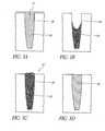
- FIG. 3Adepicts a 3-D integration via 30 filled with a dispersion 31 containing copper particles 32 after a first application of the dispersion 31 into the via 30 .
- a drying stepis performed to remove the solvent or liquid in the via 30 .
- the drying stepmay be conducted at a temperature between about 30° C. and about 100° C. in air, vacuum or inert gas. After the drying step, copper particles 32 settle down and partially fill the via 30 , as shown in FIG. 3B .
- the feature(s) filled with copper particlesis subjected to an annealing or densification step at which the copper particles are fused together, thereby forming a substantially dense copper plug 60 , as shown.
- the density of the copper plugmay be controlled by choosing the shape and size of the particles in the dispersion. While spherical particles or flat particles in the form of plates may yield high density, particles with random shapes and forms yield lower density. Mixing relatively large particles with small ones in the dispersion may also increase the density since small particles can fill the gaps between large ones. Control of density of the plug may be important to minimize stress caused by the plug on the 3-D structures.
- the annealing stepmay include a heat treatment preferably at a temperature of between about 200° C. and about 500° C., more preferably between about 300° C. and 400° C.
- heat treatmentinclude, but are not limited to, furnace annealing, laser annealing, and rapid thermal annealing (RTA).
- the atmosphere during the annealing stepmay be an inert atmosphere (Ar, He, N 2 , etc), a reducing atmosphere (H 2 , CO, alcohol vapor etc.), or vacuum.
- the dispersionmay include alloys or compounds of copper.
- metal oxide particlessuch as copper oxide
- the annealing stepmay be carried out in a reducing atmosphere at reduced pressure, atmospheric pressure or above atmospheric pressure to reduce the oxide into pure copper.
- oxide reductionis an exothermic process and releases heat helping local fusing between the particles, thereby yielding a dense copper plug.
- a mixture of copper and copper-oxide particlesmay also be used in the dispersion.
- FIG. 4illustrates a method of filling cavities on a wafer with a conductive material according to another embodiment.
- the illustrated embodimentapplies to filling particularly large features, such as for forming 3-D integration structures.
- the featurespreferably have a width of at least about 20 ⁇ m and a depth of at least about 50 ⁇ m. Since the features of the 3-D structures are large, it is possible to deliver a dispersion directly into 3-D features instead of delivering to the whole surface of the wafer.
- micro-nozzles 70are used to inject the dispersion 31 into vias 30 without delivering the dispersion to a top surface or field regions 33 of the wafer. Each of the micro-nozzles 70 are aligned over a respective one of the vias 30 .
- the dispersion 31is injected into the vias 30 .
- various apparatuses and methodsmay be used to directly fill such large features with the dispersion containing conductive particles. This configuration improves materials utilization and increases throughput. In addition, it assures that the features are filled with the dispersion without causing any voids.
- the electronic devicemay include, but is not limited to consumer electronic products, electronic circuits, electronic circuit components, parts of the consumer electronic products, electronic test equipments, etc.
- the consumer electronic productsmay include, but are not limited to, a mobile phone, a telephone, a television, a computer monitor, a computer, a hand-held computer, a personal digital assistant (PDA), a microwave, a refrigerator, a stereo system, a cassette recorder or player, a DVD player, a CD player, a VCR, an MP3 player, a radio, a camcorder, a camera, a digital camera, a portable memory chip, a washer, a dryer, a washer/dryer, a copier, a facsimile machine, a scanner, a multi functional peripheral device, a wrist watch, a clock, etc.
- the electronic devicemay include unfinished intermediate products.
Landscapes
- Engineering & Computer Science (AREA)
- Physics & Mathematics (AREA)
- Condensed Matter Physics & Semiconductors (AREA)
- General Physics & Mathematics (AREA)
- Manufacturing & Machinery (AREA)
- Computer Hardware Design (AREA)
- Microelectronics & Electronic Packaging (AREA)
- Power Engineering (AREA)
- Internal Circuitry In Semiconductor Integrated Circuit Devices (AREA)
Abstract
Description
- The present invention generally relates to semiconductor integrated circuit technology and, more particularly, to a process for filling features.
- Conventional semiconductor devices or integrated circuits (ICs) generally include a semiconductor substrate, usually a silicon substrate, and a plurality of sequentially formed dielectric layers and conductive paths or interconnects made of conductive materials. IC interconnects are usually formed by filling a conductive material such as copper into features (openings) formed in the dielectric layers. Such features include, but are not limited to, vias, cavities, and trenches that are filled to define lines, pads and contacts. In a typical integrated circuit, multiple levels of interconnect networks laterally extend with respect to the substrate surface. Interconnects formed in different layers can be electrically connected using vias filled with contacts.
- Recently, work has been carried out to develop high-density, low-capacitance vertical interconnect technologies for integrated circuit systems. These wafer level integration and packaging technologies are aimed at increasing IC system performance in terms of speed and reduced power consumption while reducing weight and volume. The vertical interconnects enable three dimensional (3-D) homogeneous integration of multiple layers of ICs as well as 3-D heterogeneous integration of multiple layers of ICs with various devices fabricated in different materials. Thus, 3-D integration includes integrating multiple ICs either at the chip or wafer level. The resulting multi-layer structures offer optimal short interconnect paths and large inter-layer signal bandwidth compared to the existing wire bonding technologies with high inductance, low speed, low wiring density and high cross talk.
- 3-D interconnect structures comprise larger features in terms of depths and widths, compared to the standard IC interconnect structures. Standard IC interconnect structures include sub-micron width vias and trenches at lower metal layers and may also have 50-100 micrometers (μm) wide lines and bond-pads, especially at the highest metal layers. Feature depth may range from 0.15-0.6 μm for lower metal levels and it may be in the range of 1-5 μm at the higher metal levels of typical IC interconnects. The aspect ratio (depth-to-width ratio) of small or narrow features in an IC interconnect is typically 2 or higher, whereas the aspect ratio of the larger features (e.g., wider than about 3 μm in the above example) are smaller than 1, typically smaller than 0.1 for lower metal layers such as M1 and M2, the lowest two levels of metal in an integrated circuit. In comparison, 3-D integration structures are much deeper. Although their widths are large, their aspect ratios are also larger than 1. In other words, the features have depths larger than their widths. These structures typically include vias with diameters or widths of 10-100 μm and aspect ratios of more than 5, even higher than 10. Therefore, processes applicable to filling the narrow features of IC interconnects with a metal do not necessarily apply to filling the wider and deeper, i.e., larger, features of 3-D interconnects.
- The most commonly used processing approach for filling a conductor into IC interconnect damascene vias or trenches is electrochemical deposition or electroplating. Electroplating techniques are relatively low cost. In addition, they have the capability of filling narrow and high aspect ratio features in a bottom-up fashion so that voids and other defects do not form in the features. In an electroplating process, a conductive material such as copper is deposited to fill such features. The material is then annealed for grain growth. Then, a material removal technique, such as chemical mechanical polishing (CMP), is employed to planarize and remove the excess metal or overburden from the top surface of the wafer, leaving conductive material only in the features. It should be noted that for IC interconnect formation it is beneficial to deposit some overburden thickness onto the top surface or field regions of the wafer surface. Such overburden helps grain growth within the small features and helps reduce resistance of copper within the features.
- 3-D integration using the IC interconnect approaches described above are challenging. First of all, deposition of continuous and uniform barrier and copper seed layers on the internal surfaces of the extremely deep vias is very difficult, if not impossible, especially for via depths of 50 μm or more.
FIGS. 1A, 1B ,2A and2B show exemplary vias of a 3-D integration structure. InFIG. 1A , a barrier layer (not shown) and aseed layer 11 are deposited on an internal surface of a via1 andfield regions 2. Then, copper is electroplated onto surfaces of theseed layer 11 in the via1 and thefield regions 2, as shown inFIG. 1B . Electroplatedcopper portion 14 is shown as cross-hatched inFIG. 1B . As shown inFIG. 1A , theseed layer 11 hasdiscontinuities discontinuities seed layer 11 yieldvoids 15 during electroplating, as shown inFIG. 1B , since electroplating of copper requires good quality copper seed layers on which copper can grow. Thevoid 15 would deteriorate the electrical properties as well as the reliability of the 3-D via.- To avoid the
void 15, the seed layer thickness may be increased to make it more continuous within the via. Then, a situation shown inFIG. 2A arises, where excess thickness at the top surface causes narrowing of the via entrance due tocopper overhang 16. With reference toFIG. 2B , upon plating copper on and into the structure ofFIG. 2A , acenter void 17 occurs due to premature closing of the via entrance during plating. Thecenter void 17 ofFIG. 2B which may be filled with the plating electrolyte deteriorates the reliability and electrical properties of a resulting 3-D structures, just as thevoid 15 ofFIG. 1B does. Other problems associated with the use of electroplating techniques for 3-D integration include low throughput, since the features to be filled are extremely large and the plating current densities are limited to a range that does not cause voiding in the vias. Such current density range is typically about 2-20 mA/cm2. - Therefore, there is a need for development of new approaches that fills the large features, such as those of 3-D integration structures, with a conductive material such as copper in a cost effective manner without voids and other defects within the features.
- According to one aspect of the invention, a method of filling a conductive material into a feature formed on a surface of a workpiece is disclosed. The method is used for filling a conductive material into a feature having a width of at least 5 micrometers and a depth of at least twice the width. The method comprises filling an ink comprising copper particles into the feature. The ink is dried so that the copper particles remain in the feature. The copper particles are annealed in the feature to form a copper structure in the feature.
- According to another aspect of the invention, a method of filling a conductive material in an opening formed in a surface of a wafer is disclosed. The method comprises filling the opening with a dispersion comprising a plurality of nanoparticles and a liquid. The liquid is removed from the opening, leaving the plurality of nanoparticles in the opening. The nanoparticles are fused in the opening to form a conductive plug.
- For purposes of summarizing the invention and the advantages achieved over the prior art, certain objects and advantages of the invention have been described above and as further described below. Of course, it is to be understood that not necessarily all such objects or advantages may be achieved in accordance with any particular embodiment of the invention. Thus, for example, those skilled in the art will recognize that the invention may be embodied or carried out in a manner that achieves or optimizes one advantage or group of advantages as taught herein without necessarily achieving other objects or advantages as may be taught or suggested herein.
- All of these embodiments are intended to be within the scope of the invention herein disclosed. These and other embodiments of the present invention will become readily apparent to those skilled in the art from the following detailed description of the preferred embodiments having reference to the attached figure, the invention not being limited to any particular preferred embodiment(s) disclosed.
FIG. 1A is a schematic cross-sectional illustration of a substrate including a 3-D integration structure feature having a thin seed layer, where the feature is to be filled with a conductive material according to a conventional electroplating method.FIG. 1B is a schematic cross-sectional illustration of the substrate ofFIG. 1A following electroplating of a conductor.FIG. 2A is a schematic cross-sectional illustration of a substrate including a 3-D integration structure feature to be filled with a conductive material having a thicker seed layer thanFIG. 1A .FIG. 2B is a schematic cross-sectional illustration of the substrate ofFIG. 2A following electroplating of a conductor.FIGS. 3A-3D are schematic cross-sectional illustrations of a method of filling 3-D integration structure features with conductive particles according to one embodiment of the invention.FIG. 4 is a schematic cross-sectional illustration of a method of filling features with conductive particles according to another embodiment of the invention.- The preferred embodiments of the present invention provide dispersion or ink deposition processes for defect-free filling of a feature (cavity or opening) formed on a surface of substrate. Preferably, the dispersion process is used to fill a feature having a large width and depth. The process may include at least two steps: a deposition step that fills a dispersion containing conductive particles into a feature; and an annealing step that fuses the conductive particles to form a conductive plug within the feature.
- In one embodiment, the process deposits or fills a conductive material into a feature with a width of at least 5 μm, preferably at least 10 μm. The feature may have an aspect ratio of at least 2. In other words, the feature has a depth of at least twice the width of the feature. In certain embodiments, the aspect ratios may be more than 5, even higher than 10. The term, “aspect ratio,” as used herein, refers to a depth-to-width ratio. The deposition step and the annealing step will now be described in detail.
- Deposition Step
- First, a composition containing conductive particles is prepared. The composition may also be referred to as a dispersion or an ink. Exemplary materials for the conductive particles are copper (Cu), copper alloys, or other conductive materials that may improve reliability of the conductive elements being formed, particularly for 3-D interconnect structures. Other examples of materials for the conductive particles include, but are not limited to, silver (Ag), nickel (Ni), gold (Au), and aluminum (Al). In certain embodiments, mixtures, alloys, or oxides of the foregoing materials may be used for the conductive particles. In the case of oxides, the particles may be non-conductive and later converted to a conductive material, as will be appreciated in view of the disclosure hereinbelow. The illustrated embodiment is suited to form conductive plugs including mixtures or alloys of conductive materials. Such conductive plugs can easily be formed by controlling the composition(s) of the particles in the dispersion. For example, by mixing controlled ratios of copper particles with silver particles within the dispersion, Cu—Ag conductive plugs may be obtained. Alternatively, particles formed of a material including both Cu and Ag (such as Cu—Ag alloys) may be used to form Cu—Ag conductive plugs.
- In one embodiment, a dispersion or an ink containing Cu is prepared. The dispersion contains nano-size particles of Cu. The Cu particles are suspended and dispersed in a solution. The particles may have an average diameter between about 1 nm and about 500 nm, preferably between about 5 nm and about 100 nm. In the illustrated embodiment, the deposition step is conducted for features that are wider than 5 μm, such that the size of the particles is not limited by the size of the opening of the features. Rather, it is dictated by the ability to obtain a uniform and well-applicable dispersion. Usually smaller particle size gives better dispersion and better ink quality. However, it is more difficult and costly to produce smaller nanoparticles. In that respect, use of inks for standard IC integration is problematic since features that are narrower than 70 nm need to be filled in that application and this would only be possible if the particle size were much smaller than 10 nm, preferably smaller than 5 nm. Preparing nanoparticle powders and dispersions or inks with such small particle sizes is not very practical because as the particle size gets smaller, the ratio of surface area (4πR2) to bulk volume (4πR3/3) of the spherical particles gets larger and larger. In this regime, particles tend to lose their copper-like properties and their characteristics are dominated more by their surface. Accordingly, it is preferred to employ larger than or equal to 5 nm size particles.
- The copper particles for use in the dispersion may be obtained by various methods. Examples of such methods include, but are not limited to, evaporation or sputtering of copper into an inert gas such as Ar or He at pressures of 10−3to 800 Torr. Various atomization or spray approaches may also be utilized.
- In one embodiment, the dispersion may be prepared by adding the copper particles obtained as above into a liquid carrier. Examples of the liquid carrier include, but are not limited to, water, alcohol, and other organic solvents such as ethylene glycol or glycerol. Additives such as surfactants and/or dispersion agents may be then added to the dispersion. The dispersion may include various surfactants and dispersing agents (cationic, anionic or neutral) commercially available, e.g., from Rohm and Haas of Philadelphia, Pa. Polyvinylpyrrolidone (PVP) is a material that may be used as an additive that helps dispersion of the particles in the dispersion. The copper particles may be in an amount between about 5 wt % and about 50 wt %, preferably between about 20 wt % and about 30 wt % of the dispersion. Then, agitation is provided, preferably through sonic vibration or sonication for the copper particles to form a stable dispersion. The viscosity of the dispersion is adjusted (by selection of particle size, carrier and percentage of nanoparticles in the dispersion) so that the dispersion flows and fills the features characteristic of 3-D structures once applied to a wafer surface.
- After the dispersion is prepared, it is deposited on a wafer surface including 3-D integration structure features such as cavities, vias, or trenches. Various approaches such as spraying, spinning, dipping, etc. may be used for application. One preferred method involves delivery of the dispersion on the wafer surface followed by spinning to get rid of excess dispersion on field regions of the wafer surface. Alternatively, the dispersion may be delivered to the whole wafer surface, and then a sweeper may sweep excess dispersion from the field regions, leaving it mainly in the cavities. It should be noted that the embodiments of the invention do not require a continuous copper seed layer on the inner walls of the 3-D structure features since it does not involve electroplating. In the illustrated embodiment, no copper seed layer is necessary provided that wetting of the via walls by the dispersion is adequate. Since the dispersion preferably contains surfactants in their formulation, once the dispersion is delivered to the wafer surface, it is pulled into the features due to the strong surface tension and fills them without any voids and defects. There are also other methods of improving void-free gap fill by the dispersion as will be described below.
- Since the weight percent of copper in the dispersion is less than 100%, the dispersion may be applied more than once onto the surface of the wafer to completely fill the features with the copper particles.
FIG. 3A depicts a 3-D integration via30 filled with adispersion 31 containingcopper particles 32 after a first application of thedispersion 31 into the via30. After the first application of thedispersion 31, a drying step is performed to remove the solvent or liquid in the via30. The drying step may be conducted at a temperature between about 30° C. and about 100° C. in air, vacuum or inert gas. After the drying step,copper particles 32 settle down and partially fill the via30, as shown inFIG. 3B . Subsequent application or applications of the dispersion followed by drying step(s) in a cyclical process eventually results in complete filling of the via30 withcopper particles 32, as shown inFIG. 3C . In the illustrated embodiment, no copper is shown on the top surface orfield regions 33 inFIG. 3C . While, there may actually be some copper particles remaining on thetop surface 33, preferably substantially all of the copper particles are within thevias 30 or other features. Preferably 2 to 4 cycles can be performed, depending on the size of a feature to be filled, the size of nanoparticles and the weight ratio ofnanoparticles 32 in thedispersion 31. There may also be annealing (see next section) performed between or part of the deposition cycles. - Annealing Step
- After the deposition step(s), the feature(s) filled with copper particles is subjected to an annealing or densification step at which the copper particles are fused together, thereby forming a substantially
dense copper plug 60, as shown. It should be noted that the density of the copper plug may be controlled by choosing the shape and size of the particles in the dispersion. While spherical particles or flat particles in the form of plates may yield high density, particles with random shapes and forms yield lower density. Mixing relatively large particles with small ones in the dispersion may also increase the density since small particles can fill the gaps between large ones. Control of density of the plug may be important to minimize stress caused by the plug on the 3-D structures. Specifically, a plug with micro-porosity may be obtained by the present technique and such a plug, although highly conductive, may induce less stress on the 3-D integration structures. The annealing step may include a heat treatment preferably at a temperature of between about 200° C. and about 500° C., more preferably between about 300° C. and 400° C. Examples of heat treatment include, but are not limited to, furnace annealing, laser annealing, and rapid thermal annealing (RTA). The atmosphere during the annealing step may be an inert atmosphere (Ar, He, N2, etc), a reducing atmosphere (H2, CO, alcohol vapor etc.), or vacuum. - In the illustrated embodiment, copper is used as an exemplary material to form the dispersion. In other embodiments, the dispersion may include alloys or compounds of copper. In one embodiment, instead of copper particles, metal oxide particles, such as copper oxide, may be used in the formulation of a dispersion. In such an embodiment, the annealing step may be carried out in a reducing atmosphere at reduced pressure, atmospheric pressure or above atmospheric pressure to reduce the oxide into pure copper. Such an embodiment can be advantageous because oxide reduction is an exothermic process and releases heat helping local fusing between the particles, thereby yielding a dense copper plug. In another embodiment, a mixture of copper and copper-oxide particles may also be used in the dispersion.
FIG. 4 illustrates a method of filling cavities on a wafer with a conductive material according to another embodiment. Preferably, the illustrated embodiment applies to filling particularly large features, such as for forming 3-D integration structures. The features preferably have a width of at least about 20 μm and a depth of at least about 50 μm. Since the features of the 3-D structures are large, it is possible to deliver a dispersion directly into 3-D features instead of delivering to the whole surface of the wafer. InFIG. 4 , micro-nozzles70 are used to inject thedispersion 31 intovias 30 without delivering the dispersion to a top surface orfield regions 33 of the wafer. Each of the micro-nozzles70 are aligned over a respective one of thevias 30. Then, thedispersion 31 is injected into thevias 30. A skilled artisan will appreciate that various apparatuses and methods may be used to directly fill such large features with the dispersion containing conductive particles. This configuration improves materials utilization and increases throughput. In addition, it assures that the features are filled with the dispersion without causing any voids.- Electronic Devices
- Another aspect of the invention provides an electronic device including an electronic circuit having an interconnect made by the method described above. The electronic device may include, but is not limited to consumer electronic products, electronic circuits, electronic circuit components, parts of the consumer electronic products, electronic test equipments, etc. The consumer electronic products may include, but are not limited to, a mobile phone, a telephone, a television, a computer monitor, a computer, a hand-held computer, a personal digital assistant (PDA), a microwave, a refrigerator, a stereo system, a cassette recorder or player, a DVD player, a CD player, a VCR, an MP3 player, a radio, a camcorder, a camera, a digital camera, a portable memory chip, a washer, a dryer, a washer/dryer, a copier, a facsimile machine, a scanner, a multi functional peripheral device, a wrist watch, a clock, etc. Further, the electronic device may include unfinished intermediate products.
- Although various preferred embodiments and the best mode have been described in detail above, those skilled in the art will readily appreciate that many modifications of the exemplary embodiment are possible without materially departing from the novel teachings and advantages of this invention.
Claims (26)
Priority Applications (2)
| Application Number | Priority Date | Filing Date | Title |
|---|---|---|---|
| US11/394,064US7485561B2 (en) | 2006-03-29 | 2006-03-29 | Filling deep features with conductors in semiconductor manufacturing |
| US11/742,302US7625814B2 (en) | 2006-03-29 | 2007-04-30 | Filling deep features with conductors in semiconductor manufacturing |
Applications Claiming Priority (1)
| Application Number | Priority Date | Filing Date | Title |
|---|---|---|---|
| US11/394,064US7485561B2 (en) | 2006-03-29 | 2006-03-29 | Filling deep features with conductors in semiconductor manufacturing |
Related Child Applications (1)
| Application Number | Title | Priority Date | Filing Date |
|---|---|---|---|
| US11/742,302Continuation-In-PartUS7625814B2 (en) | 2006-03-29 | 2007-04-30 | Filling deep features with conductors in semiconductor manufacturing |
Publications (2)
| Publication Number | Publication Date |
|---|---|
| US20070238293A1true US20070238293A1 (en) | 2007-10-11 |
| US7485561B2 US7485561B2 (en) | 2009-02-03 |
Family
ID=38575871
Family Applications (1)
| Application Number | Title | Priority Date | Filing Date |
|---|---|---|---|
| US11/394,064Active2026-04-26US7485561B2 (en) | 2006-03-29 | 2006-03-29 | Filling deep features with conductors in semiconductor manufacturing |
Country Status (1)
| Country | Link |
|---|---|
| US (1) | US7485561B2 (en) |
Cited By (5)
| Publication number | Priority date | Publication date | Assignee | Title |
|---|---|---|---|---|
| US20100200989A1 (en)* | 2009-02-12 | 2010-08-12 | Asm International, N.V. | Liner materials and related processes for 3-d integration |
| DE102009029374A1 (en)* | 2009-09-11 | 2011-04-07 | Carl Zeiss Smt Gmbh | Silicon wafer holes coating method for microlithography application, involves bringing particles with center diameter into prepared holes of substrate, and melting particles brought into prepared holes |
| DE102009029373A1 (en)* | 2009-09-11 | 2011-04-07 | Carl Zeiss Smt Gmbh | Silicon wafer holes coating method for use during manufacturing of microelectronic elements for microlithography application, involves producing beam from particles with center diameter and minimum diameter, which is larger than 5 nanometer |
| DE102010037247B4 (en)* | 2009-09-29 | 2014-01-09 | Infineon Technologies Ag | Semiconductor structure and method for its production |
| CN112018031A (en)* | 2020-09-09 | 2020-12-01 | 合肥工业大学 | Method for filling SiC through hole based on copper nanoparticles |
Families Citing this family (2)
| Publication number | Priority date | Publication date | Assignee | Title |
|---|---|---|---|---|
| JP2011159885A (en)* | 2010-02-02 | 2011-08-18 | Toshiba Corp | Method of manufacturing thin film |
| US9136166B2 (en)* | 2013-03-08 | 2015-09-15 | Taiwan Semiconductor Manufacturing Company, Ltd. | Interconnect structure and methods of making same |
Citations (46)
| Publication number | Priority date | Publication date | Assignee | Title |
|---|---|---|---|---|
| US4808273A (en)* | 1988-05-10 | 1989-02-28 | Avantek, Inc. | Method of forming completely metallized via holes in semiconductors |
| US4978639A (en)* | 1989-01-10 | 1990-12-18 | Avantek, Inc. | Method for the simultaneous formation of via-holes and wraparound plating on semiconductor chips |
| US5998292A (en)* | 1997-11-12 | 1999-12-07 | International Business Machines Corporation | Method for making three dimensional circuit integration |
| US6013948A (en)* | 1995-11-27 | 2000-01-11 | Micron Technology, Inc. | Stackable chip scale semiconductor package with mating contacts on opposed surfaces |
| US6176992B1 (en)* | 1998-11-03 | 2001-01-23 | Nutool, Inc. | Method and apparatus for electro-chemical mechanical deposition |
| US6268660B1 (en)* | 1999-03-05 | 2001-07-31 | International Business Machines Corporation | Silicon packaging with through wafer interconnects |
| US6270647B1 (en)* | 1997-09-30 | 2001-08-07 | Semitool, Inc. | Electroplating system having auxiliary electrode exterior to main reactor chamber for contact cleaning operations |
| US6270389B1 (en)* | 1995-04-04 | 2001-08-07 | Canon Kabushiki Kaisha | Method for forming an electron-emitting device using a metal-containing composition |
| US6277740B1 (en)* | 1998-08-14 | 2001-08-21 | Avery N. Goldstein | Integrated circuit trenched features and method of producing same |
| US6319384B1 (en)* | 1998-10-14 | 2001-11-20 | Faraday Technology Marketing Group, Llc | Pulse reverse electrodeposition for metallization and planarization of semiconductor substrates |
| US6319831B1 (en)* | 1999-03-18 | 2001-11-20 | Taiwan Semiconductor Manufacturing Company | Gap filling by two-step plating |
| US6333248B1 (en)* | 1999-11-11 | 2001-12-25 | Nec Corporation | Method of fabricating a semiconductor device |
| US6346479B1 (en)* | 2000-06-14 | 2002-02-12 | Advanced Micro Devices, Inc. | Method of manufacturing a semiconductor device having copper interconnects |
| US6413388B1 (en)* | 2000-02-23 | 2002-07-02 | Nutool Inc. | Pad designs and structures for a versatile materials processing apparatus |
| US6433402B1 (en)* | 2000-11-16 | 2002-08-13 | Advanced Micro Devices, Inc. | Selective copper alloy deposition |
| US6458696B1 (en)* | 2001-04-11 | 2002-10-01 | Agere Systems Guardian Corp | Plated through hole interconnections |
| US6482656B1 (en)* | 2001-06-04 | 2002-11-19 | Advanced Micro Devices, Inc. | Method of electrochemical formation of high Tc superconducting damascene interconnect for integrated circuit |
| US6492260B1 (en)* | 1998-12-02 | 2002-12-10 | Samsung Electronics Co., Ltd. | Method of fabricating damascene metal wiring |
| US20030015435A1 (en)* | 2000-05-11 | 2003-01-23 | Rimma Volodarsky | Anode assembly for plating and planarizing a conductive layer |
| US20030038038A1 (en)* | 2001-07-20 | 2003-02-27 | Basol Bulent M. | Multi step electrodeposition process for reducing defects and minimizing film thickness |
| US6534116B2 (en)* | 2000-08-10 | 2003-03-18 | Nutool, Inc. | Plating method and apparatus that creates a differential between additive disposed on a top surface and a cavity surface of a workpiece using an external influence |
| US6548395B1 (en)* | 2000-11-16 | 2003-04-15 | Advanced Micro Devices, Inc. | Method of promoting void free copper interconnects |
| US20030089986A1 (en)* | 2001-11-13 | 2003-05-15 | Daniele Gilkes | Microelectronic device layer deposited with multiple electrolytes |
| US6566259B1 (en)* | 1997-12-02 | 2003-05-20 | Applied Materials, Inc. | Integrated deposition process for copper metallization |
| US20030119311A1 (en)* | 2001-07-20 | 2003-06-26 | Basol Bulent M. | Planar metal electroprocessing |
| US6599778B2 (en)* | 2001-12-19 | 2003-07-29 | International Business Machines Corporation | Chip and wafer integration process using vertical connections |
| US6620725B1 (en)* | 1999-09-13 | 2003-09-16 | Taiwan Semiconductor Manufacturing Company | Reduction of Cu line damage by two-step CMP |
| US20040012090A1 (en)* | 2002-07-22 | 2004-01-22 | Basol Bulent M. | Defect-free thin and planar film processing |
| US6709970B1 (en)* | 2002-09-03 | 2004-03-23 | Samsung Electronics Co., Ltd. | Method for creating a damascene interconnect using a two-step electroplating process |
| US6750144B2 (en)* | 2002-02-15 | 2004-06-15 | Faraday Technology Marketing Group, Llc | Method for electrochemical metallization and planarization of semiconductor substrates having features of different sizes |
| US6762076B2 (en)* | 2002-02-20 | 2004-07-13 | Intel Corporation | Process of vertically stacking multiple wafers supporting different active integrated circuit (IC) devices |
| US20050014317A1 (en)* | 2003-07-18 | 2005-01-20 | Pyo Sung Gyu | Method for forming inductor in semiconductor device |
| US6846725B2 (en)* | 2002-10-17 | 2005-01-25 | Institute Of Microelectronics | Wafer-level package for micro-electro-mechanical systems |
| US6852627B2 (en)* | 2003-03-05 | 2005-02-08 | Micron Technology, Inc. | Conductive through wafer vias |
| US6887795B2 (en)* | 2000-05-15 | 2005-05-03 | Asm International N.V. | Method of growing electrical conductors |
| US6897148B2 (en)* | 2003-04-09 | 2005-05-24 | Tru-Si Technologies, Inc. | Electroplating and electroless plating of conductive materials into openings, and structures obtained thereby |
| US6924224B2 (en)* | 2002-10-03 | 2005-08-02 | International Business Machines Corporation | Method of forming filled blind vias |
| US6965045B2 (en)* | 2001-12-28 | 2005-11-15 | Samsung Electronics Co., Ltd. | Organic metal precursor for use in forming metal containing patterned films |
| US6975016B2 (en)* | 2002-02-06 | 2005-12-13 | Intel Corporation | Wafer bonding using a flexible bladder press and thinned wafers for three-dimensional (3D) wafer-to-wafer vertical stack integration, and application thereof |
| US20060003566A1 (en)* | 2004-06-30 | 2006-01-05 | Ismail Emesh | Methods and apparatuses for semiconductor fabrication utilizing through-wafer interconnects |
| US7019402B2 (en)* | 2003-10-17 | 2006-03-28 | International Business Machines Corporation | Silicon chip carrier with through-vias using laser assisted chemical vapor deposition of conductor |
| US7067407B2 (en)* | 2003-08-04 | 2006-06-27 | Asm International, N.V. | Method of growing electrical conductors |
| US20060139407A1 (en)* | 2004-12-24 | 2006-06-29 | Takao Umeda | Method of manufacturing an inkjet head through the anodic bonding of silicon members |
| US7098061B2 (en)* | 1999-12-21 | 2006-08-29 | Plastic Logic Limited | Forming interconnects using locally deposited solvents |
| US20060223301A1 (en)* | 2004-12-17 | 2006-10-05 | Serge Vanhaelemeersch | Formation of deep via airgaps for three dimensional wafer to wafer interconnect |
| US7148565B2 (en)* | 2002-02-20 | 2006-12-12 | Intel Corporation | Etch stop layer for silicon (Si) via etch in three-dimensional (3-D) wafer-to-wafer vertical stack |
Family Cites Families (5)
| Publication number | Priority date | Publication date | Assignee | Title |
|---|---|---|---|---|
| JP3507678B2 (en) | 1997-12-03 | 2004-03-15 | 松下電器産業株式会社 | Polishing slurry, substrate polishing apparatus and substrate polishing method |
| JP2000208443A (en) | 1999-01-13 | 2000-07-28 | Sony Corp | Method and apparatus for manufacturing electronic device |
| US6341998B1 (en) | 1999-11-04 | 2002-01-29 | Vlsi Technology, Inc. | Integrated circuit (IC) plating deposition system and method |
| US6582579B1 (en) | 2000-03-24 | 2003-06-24 | Nutool, Inc. | Methods for repairing defects on a semiconductor substrate |
| US6811658B2 (en) | 2000-06-29 | 2004-11-02 | Ebara Corporation | Apparatus for forming interconnects |
- 2006
- 2006-03-29USUS11/394,064patent/US7485561B2/enactiveActive
Patent Citations (47)
| Publication number | Priority date | Publication date | Assignee | Title |
|---|---|---|---|---|
| US4808273A (en)* | 1988-05-10 | 1989-02-28 | Avantek, Inc. | Method of forming completely metallized via holes in semiconductors |
| US4978639A (en)* | 1989-01-10 | 1990-12-18 | Avantek, Inc. | Method for the simultaneous formation of via-holes and wraparound plating on semiconductor chips |
| US6270389B1 (en)* | 1995-04-04 | 2001-08-07 | Canon Kabushiki Kaisha | Method for forming an electron-emitting device using a metal-containing composition |
| US6013948A (en)* | 1995-11-27 | 2000-01-11 | Micron Technology, Inc. | Stackable chip scale semiconductor package with mating contacts on opposed surfaces |
| US6270647B1 (en)* | 1997-09-30 | 2001-08-07 | Semitool, Inc. | Electroplating system having auxiliary electrode exterior to main reactor chamber for contact cleaning operations |
| US5998292A (en)* | 1997-11-12 | 1999-12-07 | International Business Machines Corporation | Method for making three dimensional circuit integration |
| US6566259B1 (en)* | 1997-12-02 | 2003-05-20 | Applied Materials, Inc. | Integrated deposition process for copper metallization |
| US6277740B1 (en)* | 1998-08-14 | 2001-08-21 | Avery N. Goldstein | Integrated circuit trenched features and method of producing same |
| US6319384B1 (en)* | 1998-10-14 | 2001-11-20 | Faraday Technology Marketing Group, Llc | Pulse reverse electrodeposition for metallization and planarization of semiconductor substrates |
| US6176992B1 (en)* | 1998-11-03 | 2001-01-23 | Nutool, Inc. | Method and apparatus for electro-chemical mechanical deposition |
| US6492260B1 (en)* | 1998-12-02 | 2002-12-10 | Samsung Electronics Co., Ltd. | Method of fabricating damascene metal wiring |
| US6268660B1 (en)* | 1999-03-05 | 2001-07-31 | International Business Machines Corporation | Silicon packaging with through wafer interconnects |
| US6319831B1 (en)* | 1999-03-18 | 2001-11-20 | Taiwan Semiconductor Manufacturing Company | Gap filling by two-step plating |
| US6620725B1 (en)* | 1999-09-13 | 2003-09-16 | Taiwan Semiconductor Manufacturing Company | Reduction of Cu line damage by two-step CMP |
| US6333248B1 (en)* | 1999-11-11 | 2001-12-25 | Nec Corporation | Method of fabricating a semiconductor device |
| US7098061B2 (en)* | 1999-12-21 | 2006-08-29 | Plastic Logic Limited | Forming interconnects using locally deposited solvents |
| US6413388B1 (en)* | 2000-02-23 | 2002-07-02 | Nutool Inc. | Pad designs and structures for a versatile materials processing apparatus |
| US20030015435A1 (en)* | 2000-05-11 | 2003-01-23 | Rimma Volodarsky | Anode assembly for plating and planarizing a conductive layer |
| US6887795B2 (en)* | 2000-05-15 | 2005-05-03 | Asm International N.V. | Method of growing electrical conductors |
| US6346479B1 (en)* | 2000-06-14 | 2002-02-12 | Advanced Micro Devices, Inc. | Method of manufacturing a semiconductor device having copper interconnects |
| US6534116B2 (en)* | 2000-08-10 | 2003-03-18 | Nutool, Inc. | Plating method and apparatus that creates a differential between additive disposed on a top surface and a cavity surface of a workpiece using an external influence |
| US6548395B1 (en)* | 2000-11-16 | 2003-04-15 | Advanced Micro Devices, Inc. | Method of promoting void free copper interconnects |
| US6433402B1 (en)* | 2000-11-16 | 2002-08-13 | Advanced Micro Devices, Inc. | Selective copper alloy deposition |
| US6458696B1 (en)* | 2001-04-11 | 2002-10-01 | Agere Systems Guardian Corp | Plated through hole interconnections |
| US6482656B1 (en)* | 2001-06-04 | 2002-11-19 | Advanced Micro Devices, Inc. | Method of electrochemical formation of high Tc superconducting damascene interconnect for integrated circuit |
| US20030038038A1 (en)* | 2001-07-20 | 2003-02-27 | Basol Bulent M. | Multi step electrodeposition process for reducing defects and minimizing film thickness |
| US20030119311A1 (en)* | 2001-07-20 | 2003-06-26 | Basol Bulent M. | Planar metal electroprocessing |
| US20030089986A1 (en)* | 2001-11-13 | 2003-05-15 | Daniele Gilkes | Microelectronic device layer deposited with multiple electrolytes |
| US6599778B2 (en)* | 2001-12-19 | 2003-07-29 | International Business Machines Corporation | Chip and wafer integration process using vertical connections |
| US6856025B2 (en)* | 2001-12-19 | 2005-02-15 | International Business Machines Corporation | Chip and wafer integration process using vertical connections |
| US6965045B2 (en)* | 2001-12-28 | 2005-11-15 | Samsung Electronics Co., Ltd. | Organic metal precursor for use in forming metal containing patterned films |
| US6975016B2 (en)* | 2002-02-06 | 2005-12-13 | Intel Corporation | Wafer bonding using a flexible bladder press and thinned wafers for three-dimensional (3D) wafer-to-wafer vertical stack integration, and application thereof |
| US6750144B2 (en)* | 2002-02-15 | 2004-06-15 | Faraday Technology Marketing Group, Llc | Method for electrochemical metallization and planarization of semiconductor substrates having features of different sizes |
| US6762076B2 (en)* | 2002-02-20 | 2004-07-13 | Intel Corporation | Process of vertically stacking multiple wafers supporting different active integrated circuit (IC) devices |
| US7148565B2 (en)* | 2002-02-20 | 2006-12-12 | Intel Corporation | Etch stop layer for silicon (Si) via etch in three-dimensional (3-D) wafer-to-wafer vertical stack |
| US20040012090A1 (en)* | 2002-07-22 | 2004-01-22 | Basol Bulent M. | Defect-free thin and planar film processing |
| US6709970B1 (en)* | 2002-09-03 | 2004-03-23 | Samsung Electronics Co., Ltd. | Method for creating a damascene interconnect using a two-step electroplating process |
| US6924224B2 (en)* | 2002-10-03 | 2005-08-02 | International Business Machines Corporation | Method of forming filled blind vias |
| US6846725B2 (en)* | 2002-10-17 | 2005-01-25 | Institute Of Microelectronics | Wafer-level package for micro-electro-mechanical systems |
| US6852627B2 (en)* | 2003-03-05 | 2005-02-08 | Micron Technology, Inc. | Conductive through wafer vias |
| US6897148B2 (en)* | 2003-04-09 | 2005-05-24 | Tru-Si Technologies, Inc. | Electroplating and electroless plating of conductive materials into openings, and structures obtained thereby |
| US20050014317A1 (en)* | 2003-07-18 | 2005-01-20 | Pyo Sung Gyu | Method for forming inductor in semiconductor device |
| US7067407B2 (en)* | 2003-08-04 | 2006-06-27 | Asm International, N.V. | Method of growing electrical conductors |
| US7019402B2 (en)* | 2003-10-17 | 2006-03-28 | International Business Machines Corporation | Silicon chip carrier with through-vias using laser assisted chemical vapor deposition of conductor |
| US20060003566A1 (en)* | 2004-06-30 | 2006-01-05 | Ismail Emesh | Methods and apparatuses for semiconductor fabrication utilizing through-wafer interconnects |
| US20060223301A1 (en)* | 2004-12-17 | 2006-10-05 | Serge Vanhaelemeersch | Formation of deep via airgaps for three dimensional wafer to wafer interconnect |
| US20060139407A1 (en)* | 2004-12-24 | 2006-06-29 | Takao Umeda | Method of manufacturing an inkjet head through the anodic bonding of silicon members |
Cited By (6)
| Publication number | Priority date | Publication date | Assignee | Title |
|---|---|---|---|---|
| US20100200989A1 (en)* | 2009-02-12 | 2010-08-12 | Asm International, N.V. | Liner materials and related processes for 3-d integration |
| US7884016B2 (en) | 2009-02-12 | 2011-02-08 | Asm International, N.V. | Liner materials and related processes for 3-D integration |
| DE102009029374A1 (en)* | 2009-09-11 | 2011-04-07 | Carl Zeiss Smt Gmbh | Silicon wafer holes coating method for microlithography application, involves bringing particles with center diameter into prepared holes of substrate, and melting particles brought into prepared holes |
| DE102009029373A1 (en)* | 2009-09-11 | 2011-04-07 | Carl Zeiss Smt Gmbh | Silicon wafer holes coating method for use during manufacturing of microelectronic elements for microlithography application, involves producing beam from particles with center diameter and minimum diameter, which is larger than 5 nanometer |
| DE102010037247B4 (en)* | 2009-09-29 | 2014-01-09 | Infineon Technologies Ag | Semiconductor structure and method for its production |
| CN112018031A (en)* | 2020-09-09 | 2020-12-01 | 合肥工业大学 | Method for filling SiC through hole based on copper nanoparticles |
Also Published As
| Publication number | Publication date |
|---|---|
| US7485561B2 (en) | 2009-02-03 |
Similar Documents
| Publication | Publication Date | Title |
|---|---|---|
| US7485561B2 (en) | Filling deep features with conductors in semiconductor manufacturing | |
| US6359328B1 (en) | Methods for making interconnects and diffusion barriers in integrated circuits | |
| US11121104B2 (en) | Method for manufacturing interconnect structure | |
| US7625814B2 (en) | Filling deep features with conductors in semiconductor manufacturing | |
| US10037940B2 (en) | Reliable packaging and interconnect structures | |
| US20060252254A1 (en) | Filling deep and wide openings with defect-free conductor | |
| US20030168747A1 (en) | Method of forming an air gap intermetal layer dielectric (ILD) by utilizing a dielectric material to bridge underlying metal lines | |
| US20070298607A1 (en) | Method for copper damascence fill for forming an interconnect | |
| KR20100037015A (en) | Methods of forming electrical interconnects using electroless plating techniques that inhibit void formation | |
| US7585760B2 (en) | Method for forming planarizing copper in a low-k dielectric | |
| WO2006102539A2 (en) | Method and system for electroprocessing conductive layers | |
| US7439182B2 (en) | Semiconductor device and method of fabricating the same | |
| US11911839B2 (en) | Low temperature hybrid bonding | |
| CN102959687B (en) | Method for metallising, mixture and electronic device | |
| US11398431B2 (en) | Through-silicon via for high-speed interconnects | |
| Beica et al. | Copper electrodeposition for 3D integration | |
| US20080217183A1 (en) | Electropolishing metal features on a semiconductor wafer | |
| US20080242078A1 (en) | Process of filling deep vias for 3-d integration of substrates | |
| KR100363847B1 (en) | Method of forming a metal wiring in a semiconductor device | |
| US20040248403A1 (en) | Method for forming electroless metal low resistivity interconnects | |
| EP1432016B1 (en) | A plating-rinse-plating process for fabricating copper interconnects | |
| Otake et al. | Indium Through Si Via for Quantum Chiplet Integration | |
| US20070045833A1 (en) | Copper bump barrier cap to reduce electrical resistance | |
| KR100857008B1 (en) | Metal wiring formation method of semiconductor device | |
| US20060270234A1 (en) | Method and composition for preparing a semiconductor surface for deposition of a barrier material |
Legal Events
| Date | Code | Title | Description |
|---|---|---|---|
| AS | Assignment | Owner name:ASM NUTOOL, INC., CALIFORNIA Free format text:ASSIGNMENT OF ASSIGNORS INTEREST;ASSIGNOR:BASOL, BULENT M.;REEL/FRAME:017750/0298 Effective date:20060329 | |
| AS | Assignment | Owner name:ASM NUTOOL, INC., CALIFORNIA Free format text:CHANGE OF NAME;ASSIGNOR:NUTOOL, INC.;REEL/FRAME:017518/0555 Effective date:20040729 Owner name:ASM NUTOOL, INC.,CALIFORNIA Free format text:CHANGE OF NAME;ASSIGNOR:NUTOOL, INC.;REEL/FRAME:017518/0555 Effective date:20040729 | |
| FEPP | Fee payment procedure | Free format text:PAYOR NUMBER ASSIGNED (ORIGINAL EVENT CODE: ASPN); ENTITY STATUS OF PATENT OWNER: LARGE ENTITY | |
| STCF | Information on status: patent grant | Free format text:PATENTED CASE | |
| FPAY | Fee payment | Year of fee payment:4 | |
| FPAY | Fee payment | Year of fee payment:8 | |
| MAFP | Maintenance fee payment | Free format text:PAYMENT OF MAINTENANCE FEE, 12TH YEAR, LARGE ENTITY (ORIGINAL EVENT CODE: M1553); ENTITY STATUS OF PATENT OWNER: LARGE ENTITY Year of fee payment:12 |