US20070236843A1 - Floating gate structure with high electrostatic discharge performance - Google Patents
Floating gate structure with high electrostatic discharge performanceDownload PDFInfo
- Publication number
- US20070236843A1 US20070236843A1US11/655,493US65549307AUS2007236843A1US 20070236843 A1US20070236843 A1US 20070236843A1US 65549307 AUS65549307 AUS 65549307AUS 2007236843 A1US2007236843 A1US 2007236843A1
- Authority
- US
- United States
- Prior art keywords
- diode
- semiconductor structure
- embedded
- esd
- voltage
- Prior art date
- Legal status (The legal status is an assumption and is not a legal conclusion. Google has not performed a legal analysis and makes no representation as to the accuracy of the status listed.)
- Granted
Links
- 238000007667floatingMethods0.000titleclaimsabstractdescription50
- 239000004065semiconductorSubstances0.000claimsabstractdescription31
- 230000015556catabolic processEffects0.000claimsabstractdescription27
- 230000002459sustained effectEffects0.000claimsdescription4
- 230000001960triggered effectEffects0.000claims2
- 239000010405anode materialSubstances0.000claims1
- 238000000034methodMethods0.000abstractdescription15
- 239000000463materialSubstances0.000description26
- 238000000926separation methodMethods0.000description5
- 239000000758substrateSubstances0.000description5
- 238000013461designMethods0.000description4
- 230000003247decreasing effectEffects0.000description3
- 238000004519manufacturing processMethods0.000description3
- 229910052751metalInorganic materials0.000description3
- 239000002184metalSubstances0.000description3
- 230000008569processEffects0.000description3
- 230000000295complement effectEffects0.000description2
- 230000008878couplingEffects0.000description2
- 238000010168coupling processMethods0.000description2
- 238000005859coupling reactionMethods0.000description2
- 230000005669field effectEffects0.000description2
- 238000010521absorption reactionMethods0.000description1
- 229910052782aluminiumInorganic materials0.000description1
- XAGFODPZIPBFFR-UHFFFAOYSA-NaluminiumChemical compound[Al]XAGFODPZIPBFFR-UHFFFAOYSA-N0.000description1
- 238000013459approachMethods0.000description1
- 230000009286beneficial effectEffects0.000description1
- 230000008901benefitEffects0.000description1
- 230000015572biosynthetic processEffects0.000description1
- 238000010276constructionMethods0.000description1
- 230000007547defectEffects0.000description1
- 230000001627detrimental effectEffects0.000description1
- 230000009977dual effectEffects0.000description1
- 238000005421electrostatic potentialMethods0.000description1
- 238000005516engineering processMethods0.000description1
- 239000007943implantSubstances0.000description1
- 238000002347injectionMethods0.000description1
- 239000007924injectionSubstances0.000description1
- 229910044991metal oxideInorganic materials0.000description1
- 150000004706metal oxidesChemical class0.000description1
- 230000005012migrationEffects0.000description1
- 238000013508migrationMethods0.000description1
- 230000000116mitigating effectEffects0.000description1
- 238000012986modificationMethods0.000description1
- 230000004048modificationEffects0.000description1
- 238000002161passivationMethods0.000description1
- 229910021420polycrystalline siliconInorganic materials0.000description1
- 229920005591polysiliconPolymers0.000description1
- 230000009467reductionEffects0.000description1
- 230000004044responseEffects0.000description1
- 238000012421spikingMethods0.000description1
- 238000012546transferMethods0.000description1
Images


Classifications
- H—ELECTRICITY
- H10—SEMICONDUCTOR DEVICES; ELECTRIC SOLID-STATE DEVICES NOT OTHERWISE PROVIDED FOR
- H10D—INORGANIC ELECTRIC SEMICONDUCTOR DEVICES
- H10D89/00—Aspects of integrated devices not covered by groups H10D84/00 - H10D88/00
- H10D89/60—Integrated devices comprising arrangements for electrical or thermal protection, e.g. protection circuits against electrostatic discharge [ESD]
- H10D89/601—Integrated devices comprising arrangements for electrical or thermal protection, e.g. protection circuits against electrostatic discharge [ESD] for devices having insulated gate electrodes, e.g. for IGFETs or IGBTs
- H10D89/811—Integrated devices comprising arrangements for electrical or thermal protection, e.g. protection circuits against electrostatic discharge [ESD] for devices having insulated gate electrodes, e.g. for IGFETs or IGBTs using FETs as protective elements
- H10D89/813—Integrated devices comprising arrangements for electrical or thermal protection, e.g. protection circuits against electrostatic discharge [ESD] for devices having insulated gate electrodes, e.g. for IGFETs or IGBTs using FETs as protective elements specially adapted to provide an electrical current path other than the field-effect induced current path
- H—ELECTRICITY
- H10—SEMICONDUCTOR DEVICES; ELECTRIC SOLID-STATE DEVICES NOT OTHERWISE PROVIDED FOR
- H10D—INORGANIC ELECTRIC SEMICONDUCTOR DEVICES
- H10D62/00—Semiconductor bodies, or regions thereof, of devices having potential barriers
- H10D62/10—Shapes, relative sizes or dispositions of the regions of the semiconductor bodies; Shapes of the semiconductor bodies
- H10D62/102—Constructional design considerations for preventing surface leakage or controlling electric field concentration
- H10D62/103—Constructional design considerations for preventing surface leakage or controlling electric field concentration for increasing or controlling the breakdown voltage of reverse-biased devices
- H10D62/105—Constructional design considerations for preventing surface leakage or controlling electric field concentration for increasing or controlling the breakdown voltage of reverse-biased devices by having particular doping profiles, shapes or arrangements of PN junctions; by having supplementary regions, e.g. junction termination extension [JTE]
- H10D62/108—Constructional design considerations for preventing surface leakage or controlling electric field concentration for increasing or controlling the breakdown voltage of reverse-biased devices by having particular doping profiles, shapes or arrangements of PN junctions; by having supplementary regions, e.g. junction termination extension [JTE] having localised breakdown regions, e.g. built-in avalanching regions
- H—ELECTRICITY
- H10—SEMICONDUCTOR DEVICES; ELECTRIC SOLID-STATE DEVICES NOT OTHERWISE PROVIDED FOR
- H10D—INORGANIC ELECTRIC SEMICONDUCTOR DEVICES
- H10D8/00—Diodes
- H—ELECTRICITY
- H10—SEMICONDUCTOR DEVICES; ELECTRIC SOLID-STATE DEVICES NOT OTHERWISE PROVIDED FOR
- H10D—INORGANIC ELECTRIC SEMICONDUCTOR DEVICES
- H10D8/00—Diodes
- H10D8/20—Breakdown diodes, e.g. avalanche diodes
- H10D8/25—Zener diodes
- H—ELECTRICITY
- H01—ELECTRIC ELEMENTS
- H01L—SEMICONDUCTOR DEVICES NOT COVERED BY CLASS H10
- H01L2924/00—Indexing scheme for arrangements or methods for connecting or disconnecting semiconductor or solid-state bodies as covered by H01L24/00
- H01L2924/0001—Technical content checked by a classifier
- H01L2924/0002—Not covered by any one of groups H01L24/00, H01L24/00 and H01L2224/00
Definitions
- Embodiments of the present inventionrelate to the field of integrated circuits. More specifically, embodiments of the present invention pertain to electrostatic discharge (ESD) protection for integrated circuits.
- ESDelectrostatic discharge
- An electrostatic discharge (ESD) eventoccurs when there is a transfer of energy between bodies that have different electrostatic potentials, either through contact or through an ionized ambient discharge.
- Integrated circuits (ICs) with inadequate ESD protectionare subject to catastrophic failure, including, e.g., ruptured passivation, electrothermal migration, splattered aluminum, contact spiking, dielectric failure and the like.
- an ESD eventcan damage a device even though the device continues to function. Damage of this type constitutes latent defects, which are hard to detect and significantly shorten the life of such damaged ICs.
- output drivere.g., off-chip
- the output driveritself generally provides for enhanced ESD protection through the use of a large total width of a multiple-finger structure and a wide contact-to-poly spacing.
- the gate of an output driveris connected to an internal circuit, e.g., to receive the signal to be output.
- This form of connectiongenerally makes the output device snapback much faster in response to an ESD event than if the gate of the output driver was grounded.
- a separate ESD deviceIn order to fully protect the output driver, a separate ESD device must have a trigger voltage lower than a breakdown voltage of the output driver, as well as having an ultra-low on-resistance even in a high ESD current regime.
- breakdown voltagerefers to both oxide breakdown voltage as well as junction breakdown voltage. In general, the lower of these two voltages is a point at which an integrated circuit fails to operate, and actual physical damage may occur. Either of these voltages may be lower than the other (in magnitude) depending upon a wide variety of construction and process variables.
- An ESD protection deviceshould also have a holding voltage greater than the maximum operating voltage of the circuit to prevent the circuit from turning on during an ESD event. Otherwise the circuit may be permanently damaged due to high ESD currents that cannot be sustained by the circuit itself.
- the snapback trigger voltageis greater than a breakdown voltage, damage to the integrated circuit can occur if an ESD event causes a voltage that is greater than the lowest breakdown voltage.
- MOSFETsmetal oxide semiconductor field effect transistors
- Embodiments in accordance with the present inventionembed a diode device into a floating gate electrostatic discharge protection structure.
- a semiconductor structureincludes a floating field gate device.
- the floating field gate deviceincludes an embedded diode characterized as having less temperature dependence than a Zener diode.
- the breakdown voltage of the embedded diodemay be greater than an operating voltage of an associated integrated circuit and a snapback trigger voltage of the embedded diode is lower than a breakdown voltage of the semiconductor structure.
- a semiconductor structure for electrostatic discharge protectionincludes a plurality of first fingers coupled to an output pad and a plurality of second fingers interlaced between the first fingers and coupled to a ground pad.
- the semiconductor structurefurther includes a plurality of floating field gates interposed between the first and second fingers.
- the first fingerscomprise an embedded hybrid diode characterized as having a diode breakdown voltage lower than a breakdown voltage of the semiconductor structure and a snapback trigger voltage less than the breakdown voltage of the semiconductor structure.
- a semiconductor structurein accordance with an alternative embodiment of the present invention, includes a circuit for driving an off-chip output.
- the circuitincludes a pull-down device.
- the semiconductor structurefurther includes a hybrid diode device embedded in the circuit characterized as having a trigger voltage below a breakdown voltage of the pull-down device.
- an electrostatic discharge (ESD) protection circuit for an integrated circuit (IC) for providing protection during an ESD eventincludes a current flow control component and a current flow direction control component coupled in series to the current flow control component.
- the snapback holding voltage of the electrostatic discharge protection circuitis greater than an operating voltage of the integrated circuit and a snapback trigger voltage of the electrostatic discharge protection circuit is lower than an oxide breakdown voltage of the IC.
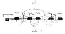
- FIG. 1Aillustrates a side sectional view of a portion of an exemplary low voltage output driver circuit with high electrostatic discharge performance, in accordance with embodiments of the present invention.
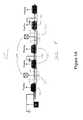
- FIG. 1Bis a detail view of an instance of a stack structure, in accordance with embodiments of the present invention.
- FIG. 2Aillustrates a plan view of a portion of exemplary low voltage output driver floating gate structure 200 with high electrostatic discharge performance, in accordance with embodiments of the present invention.
- FIG. 2Billustrates a variety of alternative layouts of an embedded hybrid diode, in accordance with embodiments of the present invention.
- a diodee.g., a Zener diode
- an output driver circuitto provide enhanced electrostatic discharge performance.
- a diodewas a separate circuit in addition to the output driver circuit.
- Embodiments in accordance with the present inventionform an embedded diode at the emitter or source of a floating gate ESD protection structure, e.g., such a diode is part of the floating gate ESD protection structure, in contrast to the conventional art method of utilizing a separate diode.
- the embedded diodeleads to a sharp decrease in trigger voltage (Vtrig), and a drastic increase in substrate current (Isub) responsive to positive electrostatic discharges.
- the large substrate currentenhances the electron injection from the emitter or source, leading to a reduction in the on-resistance due to conductivity modulation.
- the diodemay be formed in a multiple-finger field ESD device with a floating field gate. It is appreciated that the term “field gate” does not exclude a gate comprising polysilicon. In this case, the on-resistance may be reduced down to the order of tenths of an ohm. Therefore, this novel ESD structure is well suited for low-voltage output protection and enables human body model (HBM) ESD failure thresholds greater than 9 kV.
- HBMhuman body model
- FIG. 1Aillustrates a side sectional view of a portion of a floating gate structure 100 with high electrostatic discharge performance, in accordance with embodiments of the present invention.
- floating gate structure 100may be formed as part of a source and/or emitter of a floating gate ESD protection structure.
- Floating gate structure 100may, for example, be formed in p type material 160 .
- P type material 160may be a p well, an epitaxial layer or a bulk substrate. In general, p type material 160 will be at the same potential as the substrate.
- the structures illustrated in FIG. 1have substantial extent above and below the sectional plane of FIG. 1 , e.g., they extend into and out of the paper.
- Floating gate structure 100comprises a plurality of stacks 125 of n++ region 110 disposed over p+ junction 120 .
- the n++ regions 110 of stack 125are coupled to output pad 150 , which may comprise passivated metal, typically for coupling to an external pin of an integrated circuit package.
- a plurality of floating gates 130is adjacent to either side (in this view) of stacks 125 .
- floating gates 130On the other side of floating gates 130 , e.g., the side opposite from stack 125 , is a grounded region 140 of n type material.
- floating gate structure 100comprises multiple instances of a floating gate 130 , a stack 125 , a floating gate 130 and ground region 140 .
- stack 125has two adjacent floating gates 130 .
- Each ground region 140has two adjacent floating gates 130 .
- Each floating gate 130has a stack 125 on one side and a ground region 140 on the other side.
- n++ region 110floating gate 130 and n+ region 140 , in conjunction with p type material 160 , forms a p channel field effect transistor.
- Such a devicemay be used to couple output pad 150 to ground, e.g., to pull down the output terminal.
- FIG. 1Bis a detail view of an instance of stack 125 , in accordance with embodiments of the present invention.
- Stack 125comprises region 110 of n++ material disposed over region 120 of p+ material. It is to be appreciated that region 110 extends beyond (horizontally, in the view of FIG. 1B ) region 120 . For example, region 110 also contacts p type material 160 .
- stack 125forms two different types of diodes.
- Diode 107is formed between n++ region 110 , acting as a cathode, and p type material 160 , acting as an anode.
- Diode 107is a p/n type diode with a positive temperature coefficient.
- Diode 105is formed between n++ region 110 , acting as a cathode, and p+ junction 120 , acting as an anode.
- Diode 105is a Zener type diode with a negative temperature coefficient.
- the Zener diode 105generally has a lower trigger voltage than a pull down transistor formed by instance of n++ region 110 , floating gate 130 and n+ region 140 , in conjunction with p type material 160 .
- stack 125forms a novel hybrid diode structure with substantially less (in magnitude) temperature variation than diodes of the conventional art.
- the area of diode 107should be about equal to the area of diode 105 , depending upon doping concentrations, resistance, and the like. It is appreciated that other temperature coefficients for the novel hybrid diode may be desirable in alternative embodiments in accordance with the present invention, and that such other temperature coefficients may be achieved by forming differing ratios of diode areas.
- the diode breakdown voltage of floating gate structure 100may be adjusted via well known variations in doping concentrations and the like. Further, the diode breakdown voltage may be constructed so that it is different that a breakdown voltage of an associated integrated circuit, e.g., an integrated circuit protected by floating gate structure 100 . Such diode breakdown voltage(s) should be less than the breakdown voltage(s) of the associated integrated circuits.
- FIG. 2Aillustrates a plan view of a portion of exemplary floating gate structure 200 with high electrostatic discharge performance, in accordance with embodiments of the present invention.
- Floating gate structure 200is generally analogous to floating gate structure 100 of FIG. 1A , although fewer elements are illustrated.
- Floating gate structure 200comprises output pad 250 , which may comprise passivated metal, typically for coupling to an external pin of an integrated circuit package. Fingers of output pad 250 run down (in the view of FIG. 2 ) over regions of n++ material 210 . The full extent of the fingers are not shown so as to illustrate features underneath.
- the n++ material 210is disposed over regions of p+ material (obscured in the view of FIG. 2 ), as illustrated in FIG. 1 .
- regions 210 in conjunction with the underlying regions of p+ material and p type materialform a novel hybrid diode structure with a small temperature coefficient, as described previously with respect to FIG. 1B .
- Region 260is a ground pad of p+ material disposed over metal 280 . Fingers of region 280 run up (in the view of FIG. 2 ) and over n type ground regions 240 . The full extent of the fingers are not shown so as to illustrate features underneath.
- Ground pad 260picks up ground from the p well, epitaxial layer or bulk substrate.
- Floating gates 230are interposed between the fingers 210 and fingers 240 .
- the width (in the view of FIG. 2 ) of features 210plays an important role in the electrostatic discharge performance of output driver floating gate structure 200 .
- Higher ESD resistancefavors a larger width, especially a larger separation 270 between contacts and the floating gates 230 .
- die area considerationsfavor a smaller separation 270 .
- a separation 270 of about 3 to 5 ⁇ mwas found to be optimal. It is appreciated that such separation is generally much larger than the minimum design rule for contact separation for a given process.
- Floating gate structure 200exhibits a snapback holding voltage that is greater than the operating voltage of the hybrid diode 125 ( FIG. 1B ) and a snapback trigger voltage that is lower than that required to cause damage to the host integrated circuit. This electronic arrangement avoids latch up due to the snapback holding voltage being lower than the hybrid diode 125 operating voltage and IC damage due to the snapback trigger voltage being too high.
- an embedded hybrid diode 125may ensure that part of the holding voltage is sustained by the hybrid diode in conduction mode such that the remaining holding voltage is insufficient to cause latchup.
- the floating gate structure 200including hybrid diode 125 , may drain the ESD induced current, hence serving as an ESD protection device for an associated integrated circuit (IC).
- the operating voltagecannot sustain the conduction mode, forcing the hybrid diode off, thereby protecting the floating gate structure 200 and an associated integrated circuit from damage.
- FIG. 2Billustrates a variety of alternative layouts of an embedded hybrid diode, in accordance with embodiments of the present invention.
- floating field gate 231underlies n++ material 211 .
- P+ material 221is disposed above n++ material 211 .
- a plurality of p+ “islands” 222 and 223overlay n++ material 212 .
- the p+ islands 222 and 223may take a variety of shapes, including, but not limited to the illustrated circles and squares.
- “strips” of p+ material 224are formed near the edges of n++ material 213 .
- strips 224may be above or below the plane of material 213 .
- islands of p+ materiale.g., islands 222 and/or 223 , are formed near the edges of n++ material 214 .
- These and other layout alternativesmay be utilized to vary the characteristics of the novel embedded diode, in accordance with embodiments of the present invention.
- Embodiments in accordance with the present inventionprovide for systems and methods for floating gate structures with high electrostatic discharge performance. Embodiments in accordance with the present invention provide also provide for a desirable combination of snapback trigger voltage and snapback holding voltage. Further, embodiments in accordance with the present invention provide for systems and methods for forming floating gate structures with high electrostatic discharge performance that is compatible and complementary with existing systems and methods of integrated circuit design and manufacturing.
Landscapes
- Semiconductor Integrated Circuits (AREA)
- Metal-Oxide And Bipolar Metal-Oxide Semiconductor Integrated Circuits (AREA)
Abstract
Description
- This Application claims priority to U.S. Provisional Application No. 60/760,081, attorney docket VISH-8759.PRO, filed Jan. 18, 2006, entitled “Low Voltage Output Driver with High Performance Electrostatic Discharge Performance” to Luo and Demirlioglu, which is incorporated herein in its entirety by reference for all purposes.
- This application is a Continuation In Part of co-pending, commonly owned U.S. patent application Ser. No. 11/190,682, Attorney Docket No. VISH-8744, filed Jul. 26, 2005, to Luo et al., entitled “Electrostatic Discharge Protection Circuit for Integrated Circuits,” which is incorporated herein in its entirety by reference for all purposes.
- Embodiments of the present invention relate to the field of integrated circuits. More specifically, embodiments of the present invention pertain to electrostatic discharge (ESD) protection for integrated circuits.
- An electrostatic discharge (ESD) event occurs when there is a transfer of energy between bodies that have different electrostatic potentials, either through contact or through an ionized ambient discharge. Integrated circuits (ICs) with inadequate ESD protection are subject to catastrophic failure, including, e.g., ruptured passivation, electrothermal migration, splattered aluminum, contact spiking, dielectric failure and the like. Alternatively, an ESD event can damage a device even though the device continues to function. Damage of this type constitutes latent defects, which are hard to detect and significantly shorten the life of such damaged ICs.
- Under the conventional art, it is common to rely on the physical and electrical size of output (e.g., off-chip) driver circuits, to provide electrostatic discharge protection. The output driver itself generally provides for enhanced ESD protection through the use of a large total width of a multiple-finger structure and a wide contact-to-poly spacing.
- However, the effectiveness of this conventional approach to electrostatic discharge protection has been decreasing as integrated circuit technology advances. The general trend of ever smaller device geometry and decreasing circuit area favors a decreasing chip size. Accordingly, the die area available for output circuits continues to decrease, which lessens the ESD absorption/mitigation capabilities of such output circuits.
- Unfortunately, there is a growing need for even higher levels of electrostatic discharge protection than before. This promotes use of an independent ESD device in parallel with the output driver for ESD protection.
- In general, the gate of an output driver is connected to an internal circuit, e.g., to receive the signal to be output. This form of connection generally makes the output device snapback much faster in response to an ESD event than if the gate of the output driver was grounded. In order to fully protect the output driver, a separate ESD device must have a trigger voltage lower than a breakdown voltage of the output driver, as well as having an ultra-low on-resistance even in a high ESD current regime.
- As used herein, the term breakdown voltage refers to both oxide breakdown voltage as well as junction breakdown voltage. In general, the lower of these two voltages is a point at which an integrated circuit fails to operate, and actual physical damage may occur. Either of these voltages may be lower than the other (in magnitude) depending upon a wide variety of construction and process variables.
- An ESD protection device should also have a holding voltage greater than the maximum operating voltage of the circuit to prevent the circuit from turning on during an ESD event. Otherwise the circuit may be permanently damaged due to high ESD currents that cannot be sustained by the circuit itself. When the snapback trigger voltage is greater than a breakdown voltage, damage to the integrated circuit can occur if an ESD event causes a voltage that is greater than the lowest breakdown voltage.
- IC manufacturers attempt to design metal oxide semiconductor field effect transistors (MOSFETs) that have a desirable relationship between snapback trigger voltage and snapback holding voltage for use in ESD protection devices for IC applications. However, these parameters are constrained by the IC manufacturing process and by circuit performance considerations. Thus, an optimal combination of snapback trigger voltage and snapback holding voltage is not always available.
- Therefore, a need exists for systems and methods for floating gate structures with high electrostatic discharge performance. A need also exists for systems and methods for a desirable combination of snapback trigger voltage and snapback holding voltage that also satisfies the above need. A further need exists for systems and methods for floating gate structures with high electrostatic discharge performance that is compatible and complementary with existing systems and methods of integrated circuit design and manufacturing. Embodiments in accordance with the present invention provide for these needs.
- Embodiments in accordance with the present invention embed a diode device into a floating gate electrostatic discharge protection structure.
- Accordingly, systems and methods for floating gate structures with high electrostatic discharge performance are disclosed. In one embodiment, a semiconductor structure includes a floating field gate device. The floating field gate device includes an embedded diode characterized as having less temperature dependence than a Zener diode. The breakdown voltage of the embedded diode may be greater than an operating voltage of an associated integrated circuit and a snapback trigger voltage of the embedded diode is lower than a breakdown voltage of the semiconductor structure.
- In accordance with another embodiment of the present invention, a semiconductor structure for electrostatic discharge protection includes a plurality of first fingers coupled to an output pad and a plurality of second fingers interlaced between the first fingers and coupled to a ground pad. The semiconductor structure further includes a plurality of floating field gates interposed between the first and second fingers. The first fingers comprise an embedded hybrid diode characterized as having a diode breakdown voltage lower than a breakdown voltage of the semiconductor structure and a snapback trigger voltage less than the breakdown voltage of the semiconductor structure.
- In accordance with an alternative embodiment of the present invention, a semiconductor structure includes a circuit for driving an off-chip output. The circuit includes a pull-down device. The semiconductor structure further includes a hybrid diode device embedded in the circuit characterized as having a trigger voltage below a breakdown voltage of the pull-down device.
- In accordance with yet another embodiment of the present invention, an electrostatic discharge (ESD) protection circuit for an integrated circuit (IC) for providing protection during an ESD event includes a current flow control component and a current flow direction control component coupled in series to the current flow control component. The snapback holding voltage of the electrostatic discharge protection circuit is greater than an operating voltage of the integrated circuit and a snapback trigger voltage of the electrostatic discharge protection circuit is lower than an oxide breakdown voltage of the IC.
- The accompanying drawings, which are incorporated in and form a part of this specification, illustrate embodiments of the invention and, together with the description, serve to explain the principles of the invention. Unless otherwise noted, the drawings are not to scale.
FIG. 1A illustrates a side sectional view of a portion of an exemplary low voltage output driver circuit with high electrostatic discharge performance, in accordance with embodiments of the present invention.FIG. 1B is a detail view of an instance of a stack structure, in accordance with embodiments of the present invention.FIG. 2A illustrates a plan view of a portion of exemplary low voltage output driverfloating gate structure 200 with high electrostatic discharge performance, in accordance with embodiments of the present invention.FIG. 2B illustrates a variety of alternative layouts of an embedded hybrid diode, in accordance with embodiments of the present invention.- Reference will now be made in detail to various embodiments of the invention, examples of which are illustrated in the accompanying drawings. While the invention will be described in conjunction with these embodiments, it is understood that they are not intended to limit the invention to these embodiments. On the contrary, the invention is intended to cover alternatives, modifications and equivalents, which may be included within the spirit and scope of the invention as defined by the appended claims. Furthermore, in the following detailed description of the invention, numerous specific details are set forth in order to provide a thorough understanding of the invention. However, it will be recognized by one of ordinary skill in the art that the invention may be practiced without these specific details. In other instances, well known methods, procedures, components, and circuits have not been described in detail as not to unnecessarily obscure aspects of the invention.
- Under the conventional art, a diode, e.g., a Zener diode, may be utilized along side an output driver circuit to provide enhanced electrostatic discharge performance. Conventionally, such a diode was a separate circuit in addition to the output driver circuit. Embodiments in accordance with the present invention form an embedded diode at the emitter or source of a floating gate ESD protection structure, e.g., such a diode is part of the floating gate ESD protection structure, in contrast to the conventional art method of utilizing a separate diode. The embedded diode leads to a sharp decrease in trigger voltage (Vtrig), and a drastic increase in substrate current (Isub) responsive to positive electrostatic discharges. The large substrate current enhances the electron injection from the emitter or source, leading to a reduction in the on-resistance due to conductivity modulation.
- However, this benefit may be offset by a detrimental increase in the Gummel number of the device as the deep p+ implant is performed. To improve this, the diode may be formed in a multiple-finger field ESD device with a floating field gate. It is appreciated that the term “field gate” does not exclude a gate comprising polysilicon. In this case, the on-resistance may be reduced down to the order of tenths of an ohm. Therefore, this novel ESD structure is well suited for low-voltage output protection and enables human body model (HBM) ESD failure thresholds greater than 9 kV.
FIG. 1A illustrates a side sectional view of a portion of a floatinggate structure 100 with high electrostatic discharge performance, in accordance with embodiments of the present invention. For example, floatinggate structure 100 may be formed as part of a source and/or emitter of a floating gate ESD protection structure. Floatinggate structure 100 may, for example, be formed inp type material 160.P type material 160 may be a p well, an epitaxial layer or a bulk substrate. In general,p type material 160 will be at the same potential as the substrate. As may be seen inFIG. 2 , below, the structures illustrated inFIG. 1 have substantial extent above and below the sectional plane ofFIG. 1 , e.g., they extend into and out of the paper.- It is appreciated that embodiments in accordance with the present invention are well suited to formation in n type materials as well. Due to the well known duality of semiconductor structures, one of ordinary skill in the art may exchange n type conduction for p type conduction to produce alternative embodiments of the present invention. Such variations are considered within the scope of the present invention.
- Floating
gate structure 100 comprises a plurality ofstacks 125 ofn++ region 110 disposed overp+ junction 120. Then++ regions 110 ofstack 125 are coupled to output pad150, which may comprise passivated metal, typically for coupling to an external pin of an integrated circuit package. - A plurality of floating
gates 130, e.g., field oxide, is adjacent to either side (in this view) ofstacks 125. On the other side of floatinggates 130, e.g., the side opposite fromstack 125, is a groundedregion 140 of n type material. Thus floatinggate structure 100 comprises multiple instances of a floatinggate 130, astack 125, a floatinggate 130 andground region 140. - As another way of viewing floating
gate structure 100 in the view ofFIG. 1 , stack125 has two adjacent floatinggates 130. Eachground region 140 has two adjacent floatinggates 130. Each floatinggate 130 has astack 125 on one side and aground region 140 on the other side. - It is to be appreciated that an instance of
n++ region 110, floatinggate 130 andn+ region 140, in conjunction withp type material 160, forms a p channel field effect transistor. Such a device may be used to couple output pad150 to ground, e.g., to pull down the output terminal. FIG. 1B is a detail view of an instance ofstack 125, in accordance with embodiments of the present invention.Stack 125 comprisesregion 110 of n++ material disposed overregion 120 of p+ material. It is to be appreciated thatregion 110 extends beyond (horizontally, in the view ofFIG. 1B )region 120. For example,region 110 also contactsp type material 160.- It is to be further appreciated that
stack 125 forms two different types of diodes.Diode 107 is formed betweenn++ region 110, acting as a cathode, andp type material 160, acting as an anode.Diode 107 is a p/n type diode with a positive temperature coefficient.Diode 105 is formed betweenn++ region 110, acting as a cathode, andp+ junction 120, acting as an anode.Diode 105 is a Zener type diode with a negative temperature coefficient. TheZener diode 105 generally has a lower trigger voltage than a pull down transistor formed by instance ofn++ region 110, floatinggate 130 andn+ region 140, in conjunction withp type material 160. - By combining two types of diodes with opposite temperature coefficients, e.g., a diode with a positive temperature coefficient and a diode with a negative temperature coefficient, stack125 forms a novel hybrid diode structure with substantially less (in magnitude) temperature variation than diodes of the conventional art. The area of
diode 107 should be about equal to the area ofdiode 105, depending upon doping concentrations, resistance, and the like. It is appreciated that other temperature coefficients for the novel hybrid diode may be desirable in alternative embodiments in accordance with the present invention, and that such other temperature coefficients may be achieved by forming differing ratios of diode areas. - It is to be appreciated that the diode breakdown voltage of floating
gate structure 100 may be adjusted via well known variations in doping concentrations and the like. Further, the diode breakdown voltage may be constructed so that it is different that a breakdown voltage of an associated integrated circuit, e.g., an integrated circuit protected by floatinggate structure 100. Such diode breakdown voltage(s) should be less than the breakdown voltage(s) of the associated integrated circuits. FIG. 2A illustrates a plan view of a portion of exemplary floatinggate structure 200 with high electrostatic discharge performance, in accordance with embodiments of the present invention. Floatinggate structure 200 is generally analogous to floatinggate structure 100 ofFIG. 1A , although fewer elements are illustrated.- Floating
gate structure 200 comprisesoutput pad 250, which may comprise passivated metal, typically for coupling to an external pin of an integrated circuit package. Fingers ofoutput pad 250 run down (in the view ofFIG. 2 ) over regions ofn++ material 210. The full extent of the fingers are not shown so as to illustrate features underneath. Then++ material 210 is disposed over regions of p+ material (obscured in the view ofFIG. 2 ), as illustrated inFIG. 1 . As a beneficial result,regions 210 in conjunction with the underlying regions of p+ material and p type material (not shown) form a novel hybrid diode structure with a small temperature coefficient, as described previously with respect toFIG. 1B . Region 260 is a ground pad of p+ material disposed overmetal 280. Fingers ofregion 280 run up (in the view ofFIG. 2 ) and over ntype ground regions 240. The full extent of the fingers are not shown so as to illustrate features underneath.Ground pad 260 picks up ground from the p well, epitaxial layer or bulk substrate. Floatinggates 230 are interposed between thefingers 210 andfingers 240.- The width (in the view of
FIG. 2 ) offeatures 210 plays an important role in the electrostatic discharge performance of output driver floatinggate structure 200. Higher ESD resistance favors a larger width, especially alarger separation 270 between contacts and the floatinggates 230. In contrast, die area considerations favor asmaller separation 270. In an exemplary BiCMOS twin well, dual gate 0.3 μm process, aseparation 270 of about 3 to 5 μm was found to be optimal. It is appreciated that such separation is generally much larger than the minimum design rule for contact separation for a given process. - Floating
gate structure 200 exhibits a snapback holding voltage that is greater than the operating voltage of the hybrid diode125 (FIG. 1B ) and a snapback trigger voltage that is lower than that required to cause damage to the host integrated circuit. This electronic arrangement avoids latch up due to the snapback holding voltage being lower than thehybrid diode 125 operating voltage and IC damage due to the snapback trigger voltage being too high. - The use of an embedded
hybrid diode 125 may ensure that part of the holding voltage is sustained by the hybrid diode in conduction mode such that the remaining holding voltage is insufficient to cause latchup. As a result, during an ESD event the floatinggate structure 200, includinghybrid diode 125, may drain the ESD induced current, hence serving as an ESD protection device for an associated integrated circuit (IC). After the ESD event, the operating voltage cannot sustain the conduction mode, forcing the hybrid diode off, thereby protecting the floatinggate structure 200 and an associated integrated circuit from damage. FIG. 2B illustrates a variety of alternative layouts of an embedded hybrid diode, in accordance with embodiments of the present invention. Inlayout alternative 282, floatingfield gate 231 underlies n++ material211.P+ material 221 is disposed above n++ material211.- In
layout alternative 284, a plurality of p+ “islands”222 and223 overlay n++ material212. Thep+ islands layout alternative 286, “strips” ofp+ material 224 are formed near the edges ofn++ material 213. For example, strips224 may be above or below the plane ofmaterial 213. - In yet another
alternative layout 288, islands of p+ material, e.g.,islands 222 and/or223, are formed near the edges ofn++ material 214. These and other layout alternatives may be utilized to vary the characteristics of the novel embedded diode, in accordance with embodiments of the present invention. - Embodiments in accordance with the present invention provide for systems and methods for floating gate structures with high electrostatic discharge performance. Embodiments in accordance with the present invention provide also provide for a desirable combination of snapback trigger voltage and snapback holding voltage. Further, embodiments in accordance with the present invention provide for systems and methods for forming floating gate structures with high electrostatic discharge performance that is compatible and complementary with existing systems and methods of integrated circuit design and manufacturing.
- Various embodiments of the invention are thus described. While the present invention has been described in particular embodiments, it should be appreciated that the invention should not be construed as limited by such embodiments, but rather construed according to the below claims.
Claims (22)
Priority Applications (2)
| Application Number | Priority Date | Filing Date | Title |
|---|---|---|---|
| TW096101899ATWI435430B (en) | 2006-01-18 | 2007-01-18 | Low voltage output driver with high electrostatic discharge performance |
| US11/655,493US9111754B2 (en) | 2005-07-26 | 2007-01-18 | Floating gate structure with high electrostatic discharge performance |
Applications Claiming Priority (3)
| Application Number | Priority Date | Filing Date | Title |
|---|---|---|---|
| US11/190,682US7583485B1 (en) | 2005-07-26 | 2005-07-26 | Electrostatic discharge protection circuit for integrated circuits |
| US76008106P | 2006-01-18 | 2006-01-18 | |
| US11/655,493US9111754B2 (en) | 2005-07-26 | 2007-01-18 | Floating gate structure with high electrostatic discharge performance |
Related Parent Applications (1)
| Application Number | Title | Priority Date | Filing Date |
|---|---|---|---|
| US11/190,682Continuation-In-PartUS7583485B1 (en) | 2005-07-26 | 2005-07-26 | Electrostatic discharge protection circuit for integrated circuits |
Publications (2)
| Publication Number | Publication Date |
|---|---|
| US20070236843A1true US20070236843A1 (en) | 2007-10-11 |
| US9111754B2 US9111754B2 (en) | 2015-08-18 |
Family
ID=38287959
Family Applications (1)
| Application Number | Title | Priority Date | Filing Date |
|---|---|---|---|
| US11/655,493Active2026-12-01US9111754B2 (en) | 2005-07-26 | 2007-01-18 | Floating gate structure with high electrostatic discharge performance |
Country Status (7)
| Country | Link |
|---|---|
| US (1) | US9111754B2 (en) |
| EP (1) | EP1977450B1 (en) |
| JP (2) | JP2009524248A (en) |
| KR (1) | KR101139438B1 (en) |
| CN (1) | CN101361193B (en) |
| TW (1) | TWI435430B (en) |
| WO (1) | WO2007084688A1 (en) |
Cited By (2)
| Publication number | Priority date | Publication date | Assignee | Title |
|---|---|---|---|---|
| US20080135940A1 (en)* | 2005-09-30 | 2008-06-12 | Hiroyuki Hashigami | Semiconductor Device |
| US20120287969A1 (en)* | 2011-05-12 | 2012-11-15 | Ramkishore Ganti | Isolation and Protection Circuit for a Receiver in a Wireless Communication Device |
Families Citing this family (8)
| Publication number | Priority date | Publication date | Assignee | Title |
|---|---|---|---|---|
| US7544545B2 (en) | 2005-12-28 | 2009-06-09 | Vishay-Siliconix | Trench polysilicon diode |
| JP5296450B2 (en)* | 2008-08-13 | 2013-09-25 | セイコーインスツル株式会社 | Semiconductor device |
| DE102008047850B4 (en) | 2008-09-18 | 2015-08-20 | Austriamicrosystems Ag | Semiconductor body having a protective structure and method for manufacturing the same |
| CN105609500B (en)* | 2016-01-28 | 2018-10-12 | 嘉兴爱禾电子有限公司 | A kind of copolar integrated diode |
| US10381473B2 (en) | 2016-12-02 | 2019-08-13 | Vishay-Siliconix | High-electron-mobility transistor with buried interconnect |
| US10693288B2 (en) | 2018-06-26 | 2020-06-23 | Vishay SIliconix, LLC | Protection circuits with negative gate swing capability |
| US10833063B2 (en) | 2018-07-25 | 2020-11-10 | Vishay SIliconix, LLC | High electron mobility transistor ESD protection structures |
| US11632142B1 (en) | 2021-11-09 | 2023-04-18 | Macom Technology Solutions Holdings, Inc. | Hybrid diode silicon on insulator front end module and related method |
Citations (78)
| Publication number | Priority date | Publication date | Assignee | Title |
|---|---|---|---|---|
| US4922371A (en)* | 1988-11-01 | 1990-05-01 | Teledyne Semiconductor | ESD protection circuit for MOS integrated circuits |
| US5055896A (en)* | 1988-12-15 | 1991-10-08 | Siliconix Incorporated | Self-aligned LDD lateral DMOS transistor with high-voltage interconnect capability |
| US5072266A (en)* | 1988-12-27 | 1991-12-10 | Siliconix Incorporated | Trench DMOS power transistor with field-shaping body profile and three-dimensional geometry |
| US5321289A (en)* | 1992-10-22 | 1994-06-14 | Kabushiki Kaisha Toshiba | Vertical MOSFET having trench covered with multilayer gate film |
| US5374565A (en)* | 1993-10-22 | 1994-12-20 | United Microelectronics Corporation | Method for ESD protection improvement |
| US5416036A (en)* | 1993-10-04 | 1995-05-16 | United Microelectronics Corporation | Method of improvement ESD for LDD process |
| US5416351A (en)* | 1991-10-30 | 1995-05-16 | Harris Corporation | Electrostatic discharge protection |
| US5430315A (en)* | 1993-07-22 | 1995-07-04 | Rumennik; Vladimir | Bi-directional power trench MOS field effect transistor having low on-state resistance and low leakage current |
| US5455444A (en)* | 1994-04-22 | 1995-10-03 | United Microelectronics Corporation | Double polysilicon electrostatic discharge protection device for SRAM and DRAM memory devices |
| US5468667A (en)* | 1993-03-31 | 1995-11-21 | Texas Instruments Incorporated | Method of placing source contacts for efficient ESD/EOS protection in grounded substrate MOS integrated circuit |
| US5496751A (en)* | 1993-05-07 | 1996-03-05 | Vlsi Technology, Inc. | Method of forming an ESD and hot carrier resistant integrated circuit structure |
| US5500547A (en)* | 1993-12-28 | 1996-03-19 | Nec Corporation | Integrated semiconductor device with temperature sensing circuit and method for operating same |
| US5502320A (en)* | 1993-03-15 | 1996-03-26 | Kabushiki Kaisha Toshiba | Dynamic random access memory (DRAM) semiconductor device |
| US5519242A (en)* | 1994-08-17 | 1996-05-21 | David Sarnoff Research Center, Inc. | Electrostatic discharge protection circuit for a NMOS or lateral NPN transistor |
| US5529941A (en)* | 1994-03-28 | 1996-06-25 | Vlsi Technology, Inc. | Method for making an integrated circuit structure |
| US5545909A (en)* | 1994-10-19 | 1996-08-13 | Siliconix Incorporated | Electrostatic discharge protection device for integrated circuit |
| US5547880A (en)* | 1992-09-21 | 1996-08-20 | Siliconix Incorporated | Method for forming a zener diode region and an isolation region |
| US5567634A (en)* | 1995-05-01 | 1996-10-22 | National Semiconductor Corporation | Method of fabricating self-aligned contact trench DMOS transistors |
| US5581104A (en)* | 1991-01-16 | 1996-12-03 | Micron Technology, Inc. | Static discharge circuit having low breakdown voltage bipolar clamp |
| US5585299A (en)* | 1996-03-19 | 1996-12-17 | United Microelectronics Corporation | Process for fabricating a semiconductor electrostatic discharge (ESD) protective device |
| US5637900A (en)* | 1995-04-06 | 1997-06-10 | Industrial Technology Research Institute | Latchup-free fully-protected CMOS on-chip ESD protection circuit |
| US5637898A (en)* | 1995-12-22 | 1997-06-10 | North Carolina State University | Vertical field effect transistors having improved breakdown voltage capability and low on-state resistance |
| US5643820A (en)* | 1992-09-21 | 1997-07-01 | Siliconix Incorporated | Method for fabricating an MOS capacitor using zener diode region |
| US5648283A (en)* | 1992-08-07 | 1997-07-15 | Advanced Power Technology, Inc. | High density power device fabrication process using undercut oxide sidewalls |
| US5661322A (en)* | 1995-06-02 | 1997-08-26 | Siliconix Incorporated | Bidirectional blocking accumulation-mode trench power MOSFET |
| US5672527A (en)* | 1996-03-08 | 1997-09-30 | United Microelectronics Corp. | Method for fabricating an electrostatic discharge protection circuit |
| US5674761A (en)* | 1996-05-02 | 1997-10-07 | Etron Technology, Inc. | Method of making ESD protection device structure for low supply voltage applications |
| US5733794A (en)* | 1995-02-06 | 1998-03-31 | Motorola, Inc. | Process for forming a semiconductor device with ESD protection |
| US5850095A (en)* | 1996-09-24 | 1998-12-15 | Texas Instruments Incorporated | ESD protection circuit using zener diode and interdigitated NPN transistor |
| US5932916A (en)* | 1997-09-26 | 1999-08-03 | Lg Semicon Co., Ltd. | Electrostatic discharge protection circuit |
| US5953601A (en)* | 1998-02-17 | 1999-09-14 | Taiwan Semiconductor Manufacturing Company, Ltd. | ESD implantation scheme for 0.35 μm 3.3V 70A gate oxide process |
| US5998837A (en)* | 1995-06-02 | 1999-12-07 | Siliconix Incorporated | Trench-gated power MOSFET with protective diode having adjustable breakdown voltage |
| US5998836A (en)* | 1995-06-02 | 1999-12-07 | Siliconix Incorporated | Trench-gated power MOSFET with protective diode |
| US5998833A (en)* | 1998-10-26 | 1999-12-07 | North Carolina State University | Power semiconductor devices having improved high frequency switching and breakdown characteristics |
| US6044018A (en)* | 1998-06-17 | 2000-03-28 | Mosel Vitelic, Inc. | Single-poly flash memory cell for embedded application and related methods |
| US6046470A (en)* | 1995-10-02 | 2000-04-04 | Siliconix Incorporated | Trench-gated MOSFET with integral temperature detection diode |
| US6049108A (en)* | 1995-06-02 | 2000-04-11 | Siliconix Incorporated | Trench-gated MOSFET with bidirectional voltage clamping |
| US6060752A (en)* | 1997-12-31 | 2000-05-09 | Siliconix, Incorporated | Electrostatic discharge protection circuit |
| US6078090A (en)* | 1997-04-02 | 2000-06-20 | Siliconix Incorporated | Trench-gated Schottky diode with integral clamping diode |
| US6140678A (en)* | 1995-06-02 | 2000-10-31 | Siliconix Incorporated | Trench-gated power MOSFET with protective diode |
| US6168996B1 (en)* | 1997-08-28 | 2001-01-02 | Hitachi, Ltd. | Method of fabricating semiconductor device |
| US6211018B1 (en)* | 1999-08-14 | 2001-04-03 | Electronics And Telecommunications Research Institute | Method for fabricating high density trench gate type power device |
| US6255683B1 (en)* | 1998-12-29 | 2001-07-03 | Infineon Technologies Ag | Dynamic random access memory |
| US6268242B1 (en)* | 1997-12-31 | 2001-07-31 | Richard K. Williams | Method of forming vertical mosfet device having voltage clamped gate and self-aligned contact |
| US6277695B1 (en)* | 1999-04-16 | 2001-08-21 | Siliconix Incorporated | Method of forming vertical planar DMOSFET with self-aligned contact |
| US6347026B1 (en)* | 1999-05-26 | 2002-02-12 | Lsi Logic Corporation | Input and power protection circuit implemented in a complementary metal oxide semiconductor process using salicides |
| US20020030231A1 (en)* | 2000-05-31 | 2002-03-14 | Seiko Epson Corporation | Semiconductor device having electrostatic protection circuit and method of fabricating the same |
| US6365462B2 (en)* | 1999-05-28 | 2002-04-02 | Micro-Ohm Corporation | Methods of forming power semiconductor devices having tapered trench-based insulating regions therein |
| US6365941B1 (en)* | 1998-09-29 | 2002-04-02 | Samsung Electronics Co., Ltd. | Electro-static discharge circuit of semiconductor device, structure thereof and method for fabricating the structure |
| US6368922B1 (en)* | 1996-04-02 | 2002-04-09 | Winbond Electronics Corporation | Internal ESD protection structure with contact diffusion |
| US6391721B2 (en)* | 1999-01-27 | 2002-05-21 | Fujitsu Limited | Non-volatile semiconductor memory device having vertical transistors and fabrication method therefor |
| US20020063289A1 (en)* | 2000-11-30 | 2002-05-30 | Kung-Yen Su | Field oxide device with zener junction for electrostatic discharge (ESD) protection and other applications |
| US20020074585A1 (en)* | 1988-05-17 | 2002-06-20 | Advanced Power Technology, Inc., Delaware Corporation | Self-aligned power MOSFET with enhanced base region |
| US6413822B2 (en)* | 1999-04-22 | 2002-07-02 | Advanced Analogic Technologies, Inc. | Super-self-aligned fabrication process of trench-gate DMOS with overlying device layer |
| US6514839B1 (en)* | 2001-10-05 | 2003-02-04 | Taiwan Semiconductor Manufacturing Company | ESD implantation method in deep-submicron CMOS technology for high-voltage-tolerant applications with light-doping concentrations |
| US20030030092A1 (en)* | 2001-08-10 | 2003-02-13 | Darwish Mohamed N. | Trench MIS device with reduced gate-to-drain capacitance |
| US6548860B1 (en)* | 2000-02-29 | 2003-04-15 | General Semiconductor, Inc. | DMOS transistor structure having improved performance |
| US20030071310A1 (en)* | 2001-10-11 | 2003-04-17 | Salling Craig T. | Method to increase substrate potential in MOS transistors used in ESD protection circuits |
| US6642109B2 (en)* | 2001-12-22 | 2003-11-04 | Hynix Semiconductor Inc. | Method of manufacturing a flash memory cell |
| US6645802B1 (en)* | 1999-02-11 | 2003-11-11 | Xilinx, Inc. | Method of forming a zener diode |
| US6661054B1 (en)* | 1998-03-05 | 2003-12-09 | Mitsubishi Denki Kabushiki Kaisha | Semiconductor device and method of fabricating the same |
| US6680833B2 (en)* | 1999-12-27 | 2004-01-20 | Nec Electronics Corporation | Input-output protection device for semiconductor integrated circuit |
| US6700158B1 (en)* | 2000-08-18 | 2004-03-02 | Fairchild Semiconductor Corporation | Trench corner protection for trench MOSFET |
| US20040075145A1 (en)* | 2002-10-18 | 2004-04-22 | Shibib Muhammed Ayman | Electrostatic discharge protection in a semiconductor device |
| US20040124472A1 (en)* | 2002-12-30 | 2004-07-01 | Shi-Tron Lin | Electrostatic discharge (ESD) protection device |
| US6815775B2 (en)* | 2001-02-02 | 2004-11-09 | Industrial Technology Research Institute | ESD protection design with turn-on restraining method and structures |
| US6855593B2 (en)* | 2002-07-11 | 2005-02-15 | International Rectifier Corporation | Trench Schottky barrier diode |
| US20050036251A1 (en)* | 2003-08-12 | 2005-02-17 | Micrel, Incorporated | Electrostatic discharge protection for trim-diodes |
| US6861701B2 (en)* | 2003-03-05 | 2005-03-01 | Advanced Analogic Technologies, Inc. | Trench power MOSFET with planarized gate bus |
| US6919603B2 (en)* | 2003-04-30 | 2005-07-19 | Texas Instruments Incorporated | Efficient protection structure for reverse pin-to-pin electrostatic discharge |
| US6927455B2 (en)* | 2002-12-25 | 2005-08-09 | Mitsubishi Denki Kabushiki Kaisha | Power semiconductor device having semiconductor-layer-forming position controlled by ion implantation without using photoresist pattern, and method of manufacturing such power semiconductor device |
| US7019368B1 (en)* | 2003-07-11 | 2006-03-28 | Actel Corporation | Low-capacitance input/output and electrostatic discharge circuit for protecting an integrated circuit from electrostatic discharge |
| US20060208340A1 (en)* | 2005-03-15 | 2006-09-21 | Glenn Jack L | Protection device for handling energy transients |
| US20060268479A1 (en)* | 2005-05-31 | 2006-11-30 | Atmel Germany Gmbh | ESD protection structure |
| US7544545B2 (en)* | 2005-12-28 | 2009-06-09 | Vishay-Siliconix | Trench polysilicon diode |
| US7583485B1 (en)* | 2005-07-26 | 2009-09-01 | Vishay-Siliconix | Electrostatic discharge protection circuit for integrated circuits |
| US7781826B2 (en)* | 2006-11-16 | 2010-08-24 | Alpha & Omega Semiconductor, Ltd. | Circuit configuration and manufacturing processes for vertical transient voltage suppressor (TVS) and EMI filter |
| US8629019B2 (en)* | 2002-09-24 | 2014-01-14 | Vishay-Siliconix | Method of forming self aligned contacts for a power MOSFET |
Family Cites Families (27)
| Publication number | Priority date | Publication date | Assignee | Title |
|---|---|---|---|---|
| US4677369A (en) | 1985-09-19 | 1987-06-30 | Precision Monolithics, Inc. | CMOS temperature insensitive voltage reference |
| US4748103A (en) | 1986-03-21 | 1988-05-31 | Advanced Power Technology | Mask-surrogate semiconductor process employing dopant protective region |
| JP2667392B2 (en) | 1986-09-26 | 1997-10-27 | 株式会社デンソー | Method for manufacturing polycrystalline semiconductor diode |
| JPH0590520A (en)* | 1991-09-26 | 1993-04-09 | Nissan Motor Co Ltd | Semiconductor protective device |
| JPH05291501A (en)* | 1992-04-13 | 1993-11-05 | Nissan Motor Co Ltd | Semiconductor protective device |
| GB9306895D0 (en) | 1993-04-01 | 1993-05-26 | Philips Electronics Uk Ltd | A method of manufacturing a semiconductor device comprising an insulated gate field effect device |
| JPH07273320A (en) | 1994-03-31 | 1995-10-20 | Toshiba Corp | Semiconductor device |
| JPH09129877A (en) | 1995-10-30 | 1997-05-16 | Toyota Central Res & Dev Lab Inc | Semiconductor device manufacturing method, insulated gate semiconductor device manufacturing method, and insulated gate semiconductor device |
| US5882967A (en)* | 1997-05-07 | 1999-03-16 | International Business Machines Corporation | Process for buried diode formation in CMOS |
| JPH11233641A (en)* | 1998-02-10 | 1999-08-27 | Seiko Epson Corp | Semiconductor device and method of manufacturing semiconductor device |
| JP3413569B2 (en) | 1998-09-16 | 2003-06-03 | 株式会社日立製作所 | Insulated gate semiconductor device and method of manufacturing the same |
| JP3574359B2 (en)* | 1998-09-18 | 2004-10-06 | セイコーエプソン株式会社 | Semiconductor device |
| JP3708764B2 (en)* | 1999-09-07 | 2005-10-19 | Necエレクトロニクス株式会社 | Semiconductor device |
| JP3348711B2 (en)* | 1999-12-03 | 2002-11-20 | セイコーエプソン株式会社 | Semiconductor device and method of manufacturing the same |
| JP2001257349A (en) | 2000-03-09 | 2001-09-21 | Sanyo Electric Co Ltd | MOSFET protection device |
| JP2002016080A (en) | 2000-06-28 | 2002-01-18 | Toshiba Corp | Manufacturing method of trench gate type MOSFET |
| JP2002110978A (en) | 2000-10-02 | 2002-04-12 | Toshiba Corp | Power semiconductor device |
| JP2002208677A (en) | 2001-01-12 | 2002-07-26 | Toyota Industries Corp | Semiconductor device with temperature detection function |
| JP4932088B2 (en) | 2001-02-19 | 2012-05-16 | ルネサスエレクトロニクス株式会社 | Insulated gate type semiconductor device manufacturing method |
| JP2002270841A (en) | 2001-03-13 | 2002-09-20 | Denso Corp | Semiconductor device and manufacturing method thereof |
| JP2002274640A (en) | 2001-03-19 | 2002-09-25 | Honda Motor Co Ltd | Pallet stopper device |
| KR100954471B1 (en) | 2001-11-02 | 2010-04-22 | 페어차일드 세미컨덕터 코포레이션 | ESD NMOS devices and formation methods, and systems including the same |
| US6838722B2 (en) | 2002-03-22 | 2005-01-04 | Siliconix Incorporated | Structures of and methods of fabricating trench-gated MIS devices |
| JP2004247455A (en)* | 2003-02-13 | 2004-09-02 | Seiko Epson Corp | Semiconductor device |
| JP2004296883A (en)* | 2003-03-27 | 2004-10-21 | Sharp Corp | Semiconductor device and manufacturing method thereof |
| US7129557B2 (en) | 2004-05-25 | 2006-10-31 | International Business Machines Corporation | Autonomic thermal monitor and controller for thin film devices |
| JP2011233641A (en) | 2010-04-26 | 2011-11-17 | Disco Abrasive Syst Ltd | Laser processing method for plate-like object |
- 2007
- 2007-01-18CNCN2007800016046Apatent/CN101361193B/enactiveActive
- 2007-01-18TWTW096101899Apatent/TWI435430B/enactive
- 2007-01-18JPJP2008551423Apatent/JP2009524248A/enactivePending
- 2007-01-18KRKR1020087013982Apatent/KR101139438B1/enactiveActive
- 2007-01-18EPEP07718296.2Apatent/EP1977450B1/enactiveActive
- 2007-01-18WOPCT/US2007/001473patent/WO2007084688A1/enactiveApplication Filing
- 2007-01-18USUS11/655,493patent/US9111754B2/enactiveActive
- 2013
- 2013-01-09JPJP2013001443Apatent/JP5738903B2/enactiveActive
Patent Citations (88)
| Publication number | Priority date | Publication date | Assignee | Title |
|---|---|---|---|---|
| US20020074585A1 (en)* | 1988-05-17 | 2002-06-20 | Advanced Power Technology, Inc., Delaware Corporation | Self-aligned power MOSFET with enhanced base region |
| US4922371A (en)* | 1988-11-01 | 1990-05-01 | Teledyne Semiconductor | ESD protection circuit for MOS integrated circuits |
| US5055896A (en)* | 1988-12-15 | 1991-10-08 | Siliconix Incorporated | Self-aligned LDD lateral DMOS transistor with high-voltage interconnect capability |
| US5072266A (en)* | 1988-12-27 | 1991-12-10 | Siliconix Incorporated | Trench DMOS power transistor with field-shaping body profile and three-dimensional geometry |
| US5581104A (en)* | 1991-01-16 | 1996-12-03 | Micron Technology, Inc. | Static discharge circuit having low breakdown voltage bipolar clamp |
| US5416351A (en)* | 1991-10-30 | 1995-05-16 | Harris Corporation | Electrostatic discharge protection |
| US5648283A (en)* | 1992-08-07 | 1997-07-15 | Advanced Power Technology, Inc. | High density power device fabrication process using undercut oxide sidewalls |
| US5547880A (en)* | 1992-09-21 | 1996-08-20 | Siliconix Incorporated | Method for forming a zener diode region and an isolation region |
| US5643820A (en)* | 1992-09-21 | 1997-07-01 | Siliconix Incorporated | Method for fabricating an MOS capacitor using zener diode region |
| US5321289A (en)* | 1992-10-22 | 1994-06-14 | Kabushiki Kaisha Toshiba | Vertical MOSFET having trench covered with multilayer gate film |
| US5502320A (en)* | 1993-03-15 | 1996-03-26 | Kabushiki Kaisha Toshiba | Dynamic random access memory (DRAM) semiconductor device |
| US5468667A (en)* | 1993-03-31 | 1995-11-21 | Texas Instruments Incorporated | Method of placing source contacts for efficient ESD/EOS protection in grounded substrate MOS integrated circuit |
| US5496751A (en)* | 1993-05-07 | 1996-03-05 | Vlsi Technology, Inc. | Method of forming an ESD and hot carrier resistant integrated circuit structure |
| US5430315A (en)* | 1993-07-22 | 1995-07-04 | Rumennik; Vladimir | Bi-directional power trench MOS field effect transistor having low on-state resistance and low leakage current |
| US5416036A (en)* | 1993-10-04 | 1995-05-16 | United Microelectronics Corporation | Method of improvement ESD for LDD process |
| US5559352A (en)* | 1993-10-22 | 1996-09-24 | United Microelectronics Corporation | ESD protection improvement |
| US5374565A (en)* | 1993-10-22 | 1994-12-20 | United Microelectronics Corporation | Method for ESD protection improvement |
| US5500547A (en)* | 1993-12-28 | 1996-03-19 | Nec Corporation | Integrated semiconductor device with temperature sensing circuit and method for operating same |
| US5529941A (en)* | 1994-03-28 | 1996-06-25 | Vlsi Technology, Inc. | Method for making an integrated circuit structure |
| US5455444A (en)* | 1994-04-22 | 1995-10-03 | United Microelectronics Corporation | Double polysilicon electrostatic discharge protection device for SRAM and DRAM memory devices |
| US5519242A (en)* | 1994-08-17 | 1996-05-21 | David Sarnoff Research Center, Inc. | Electrostatic discharge protection circuit for a NMOS or lateral NPN transistor |
| US5545909A (en)* | 1994-10-19 | 1996-08-13 | Siliconix Incorporated | Electrostatic discharge protection device for integrated circuit |
| US5654574A (en)* | 1994-10-19 | 1997-08-05 | Siliconix Incorporated | Electrostatic discharge protection device for integrated circuit |
| US5877534A (en)* | 1994-10-19 | 1999-03-02 | Siliconix Incorporated | Method of forming electrostatic discharge protection device for integrated circuit |
| US5677205A (en)* | 1994-10-19 | 1997-10-14 | Siliconix Incorporated | Method for forming electrostatic discharge protection device for integrated circuit |
| US5733794A (en)* | 1995-02-06 | 1998-03-31 | Motorola, Inc. | Process for forming a semiconductor device with ESD protection |
| US5637900A (en)* | 1995-04-06 | 1997-06-10 | Industrial Technology Research Institute | Latchup-free fully-protected CMOS on-chip ESD protection circuit |
| US5567634A (en)* | 1995-05-01 | 1996-10-22 | National Semiconductor Corporation | Method of fabricating self-aligned contact trench DMOS transistors |
| US5998837A (en)* | 1995-06-02 | 1999-12-07 | Siliconix Incorporated | Trench-gated power MOSFET with protective diode having adjustable breakdown voltage |
| US5661322A (en)* | 1995-06-02 | 1997-08-26 | Siliconix Incorporated | Bidirectional blocking accumulation-mode trench power MOSFET |
| US5998836A (en)* | 1995-06-02 | 1999-12-07 | Siliconix Incorporated | Trench-gated power MOSFET with protective diode |
| US6140678A (en)* | 1995-06-02 | 2000-10-31 | Siliconix Incorporated | Trench-gated power MOSFET with protective diode |
| US6049108A (en)* | 1995-06-02 | 2000-04-11 | Siliconix Incorporated | Trench-gated MOSFET with bidirectional voltage clamping |
| US6046470A (en)* | 1995-10-02 | 2000-04-04 | Siliconix Incorporated | Trench-gated MOSFET with integral temperature detection diode |
| US5637898A (en)* | 1995-12-22 | 1997-06-10 | North Carolina State University | Vertical field effect transistors having improved breakdown voltage capability and low on-state resistance |
| US5672527A (en)* | 1996-03-08 | 1997-09-30 | United Microelectronics Corp. | Method for fabricating an electrostatic discharge protection circuit |
| US5585299A (en)* | 1996-03-19 | 1996-12-17 | United Microelectronics Corporation | Process for fabricating a semiconductor electrostatic discharge (ESD) protective device |
| US6368922B1 (en)* | 1996-04-02 | 2002-04-09 | Winbond Electronics Corporation | Internal ESD protection structure with contact diffusion |
| US5674761A (en)* | 1996-05-02 | 1997-10-07 | Etron Technology, Inc. | Method of making ESD protection device structure for low supply voltage applications |
| US5850095A (en)* | 1996-09-24 | 1998-12-15 | Texas Instruments Incorporated | ESD protection circuit using zener diode and interdigitated NPN transistor |
| US6078090A (en)* | 1997-04-02 | 2000-06-20 | Siliconix Incorporated | Trench-gated Schottky diode with integral clamping diode |
| US6168996B1 (en)* | 1997-08-28 | 2001-01-02 | Hitachi, Ltd. | Method of fabricating semiconductor device |
| US5932916A (en)* | 1997-09-26 | 1999-08-03 | Lg Semicon Co., Ltd. | Electrostatic discharge protection circuit |
| US6268242B1 (en)* | 1997-12-31 | 2001-07-31 | Richard K. Williams | Method of forming vertical mosfet device having voltage clamped gate and self-aligned contact |
| US6060752A (en)* | 1997-12-31 | 2000-05-09 | Siliconix, Incorporated | Electrostatic discharge protection circuit |
| US5953601A (en)* | 1998-02-17 | 1999-09-14 | Taiwan Semiconductor Manufacturing Company, Ltd. | ESD implantation scheme for 0.35 μm 3.3V 70A gate oxide process |
| US6661054B1 (en)* | 1998-03-05 | 2003-12-09 | Mitsubishi Denki Kabushiki Kaisha | Semiconductor device and method of fabricating the same |
| US6044018A (en)* | 1998-06-17 | 2000-03-28 | Mosel Vitelic, Inc. | Single-poly flash memory cell for embedded application and related methods |
| US6365941B1 (en)* | 1998-09-29 | 2002-04-02 | Samsung Electronics Co., Ltd. | Electro-static discharge circuit of semiconductor device, structure thereof and method for fabricating the structure |
| US5998833A (en)* | 1998-10-26 | 1999-12-07 | North Carolina State University | Power semiconductor devices having improved high frequency switching and breakdown characteristics |
| US6255683B1 (en)* | 1998-12-29 | 2001-07-03 | Infineon Technologies Ag | Dynamic random access memory |
| US6391721B2 (en)* | 1999-01-27 | 2002-05-21 | Fujitsu Limited | Non-volatile semiconductor memory device having vertical transistors and fabrication method therefor |
| US6645802B1 (en)* | 1999-02-11 | 2003-11-11 | Xilinx, Inc. | Method of forming a zener diode |
| US6277695B1 (en)* | 1999-04-16 | 2001-08-21 | Siliconix Incorporated | Method of forming vertical planar DMOSFET with self-aligned contact |
| US6413822B2 (en)* | 1999-04-22 | 2002-07-02 | Advanced Analogic Technologies, Inc. | Super-self-aligned fabrication process of trench-gate DMOS with overlying device layer |
| US6347026B1 (en)* | 1999-05-26 | 2002-02-12 | Lsi Logic Corporation | Input and power protection circuit implemented in a complementary metal oxide semiconductor process using salicides |
| US6365462B2 (en)* | 1999-05-28 | 2002-04-02 | Micro-Ohm Corporation | Methods of forming power semiconductor devices having tapered trench-based insulating regions therein |
| US6211018B1 (en)* | 1999-08-14 | 2001-04-03 | Electronics And Telecommunications Research Institute | Method for fabricating high density trench gate type power device |
| US6680833B2 (en)* | 1999-12-27 | 2004-01-20 | Nec Electronics Corporation | Input-output protection device for semiconductor integrated circuit |
| US6548860B1 (en)* | 2000-02-29 | 2003-04-15 | General Semiconductor, Inc. | DMOS transistor structure having improved performance |
| US20020030231A1 (en)* | 2000-05-31 | 2002-03-14 | Seiko Epson Corporation | Semiconductor device having electrostatic protection circuit and method of fabricating the same |
| US6700158B1 (en)* | 2000-08-18 | 2004-03-02 | Fairchild Semiconductor Corporation | Trench corner protection for trench MOSFET |
| US6631060B2 (en)* | 2000-11-30 | 2003-10-07 | Winbond Electronics Corporation | Field oxide device with zener junction for electrostatic discharge (ESD) protection and other applications |
| US20020063289A1 (en)* | 2000-11-30 | 2002-05-30 | Kung-Yen Su | Field oxide device with zener junction for electrostatic discharge (ESD) protection and other applications |
| US6815775B2 (en)* | 2001-02-02 | 2004-11-09 | Industrial Technology Research Institute | ESD protection design with turn-on restraining method and structures |
| US20030030092A1 (en)* | 2001-08-10 | 2003-02-13 | Darwish Mohamed N. | Trench MIS device with reduced gate-to-drain capacitance |
| US6514839B1 (en)* | 2001-10-05 | 2003-02-04 | Taiwan Semiconductor Manufacturing Company | ESD implantation method in deep-submicron CMOS technology for high-voltage-tolerant applications with light-doping concentrations |
| US20030071310A1 (en)* | 2001-10-11 | 2003-04-17 | Salling Craig T. | Method to increase substrate potential in MOS transistors used in ESD protection circuits |
| US6642109B2 (en)* | 2001-12-22 | 2003-11-04 | Hynix Semiconductor Inc. | Method of manufacturing a flash memory cell |
| US6855593B2 (en)* | 2002-07-11 | 2005-02-15 | International Rectifier Corporation | Trench Schottky barrier diode |
| US8629019B2 (en)* | 2002-09-24 | 2014-01-14 | Vishay-Siliconix | Method of forming self aligned contacts for a power MOSFET |
| US20040075145A1 (en)* | 2002-10-18 | 2004-04-22 | Shibib Muhammed Ayman | Electrostatic discharge protection in a semiconductor device |
| US6927455B2 (en)* | 2002-12-25 | 2005-08-09 | Mitsubishi Denki Kabushiki Kaisha | Power semiconductor device having semiconductor-layer-forming position controlled by ion implantation without using photoresist pattern, and method of manufacturing such power semiconductor device |
| US20040124472A1 (en)* | 2002-12-30 | 2004-07-01 | Shi-Tron Lin | Electrostatic discharge (ESD) protection device |
| US6861701B2 (en)* | 2003-03-05 | 2005-03-01 | Advanced Analogic Technologies, Inc. | Trench power MOSFET with planarized gate bus |
| US7419878B2 (en)* | 2003-03-05 | 2008-09-02 | Advanced Analogic Technologies, Inc. | Planarized and silicided trench contact |
| US6919603B2 (en)* | 2003-04-30 | 2005-07-19 | Texas Instruments Incorporated | Efficient protection structure for reverse pin-to-pin electrostatic discharge |
| US7482218B1 (en)* | 2003-07-11 | 2009-01-27 | Actel Corporation | Low-capacitance input/output and electrostatic discharge circuit for protecting an integrated circuit from electrostatic discharge |
| US7019368B1 (en)* | 2003-07-11 | 2006-03-28 | Actel Corporation | Low-capacitance input/output and electrostatic discharge circuit for protecting an integrated circuit from electrostatic discharge |
| US20050036251A1 (en)* | 2003-08-12 | 2005-02-17 | Micrel, Incorporated | Electrostatic discharge protection for trim-diodes |
| US20060208340A1 (en)* | 2005-03-15 | 2006-09-21 | Glenn Jack L | Protection device for handling energy transients |
| US20060268479A1 (en)* | 2005-05-31 | 2006-11-30 | Atmel Germany Gmbh | ESD protection structure |
| US7583485B1 (en)* | 2005-07-26 | 2009-09-01 | Vishay-Siliconix | Electrostatic discharge protection circuit for integrated circuits |
| US8582258B1 (en)* | 2005-07-26 | 2013-11-12 | Vishay-Siliconix | Electrostatic discharge protection circuit for integrated circuits |
| US7544545B2 (en)* | 2005-12-28 | 2009-06-09 | Vishay-Siliconix | Trench polysilicon diode |
| US7612431B2 (en)* | 2005-12-28 | 2009-11-03 | Vishay-Siliconix | Trench polysilicon diode |
| US8072013B1 (en)* | 2005-12-28 | 2011-12-06 | Vishay-Siliconix | Trench polysilicon diode |
| US7781826B2 (en)* | 2006-11-16 | 2010-08-24 | Alpha & Omega Semiconductor, Ltd. | Circuit configuration and manufacturing processes for vertical transient voltage suppressor (TVS) and EMI filter |
Cited By (3)
| Publication number | Priority date | Publication date | Assignee | Title |
|---|---|---|---|---|
| US20080135940A1 (en)* | 2005-09-30 | 2008-06-12 | Hiroyuki Hashigami | Semiconductor Device |
| US20120287969A1 (en)* | 2011-05-12 | 2012-11-15 | Ramkishore Ganti | Isolation and Protection Circuit for a Receiver in a Wireless Communication Device |
| US9124354B2 (en)* | 2011-05-12 | 2015-09-01 | St-Ericsson Sa | Isolation and protection circuit for a receiver in a wireless communication device |
Also Published As
| Publication number | Publication date |
|---|---|
| TW200735324A (en) | 2007-09-16 |
| TWI435430B (en) | 2014-04-21 |
| WO2007084688A1 (en) | 2007-07-26 |
| CN101361193A (en) | 2009-02-04 |
| CN101361193B (en) | 2013-07-10 |
| JP5738903B2 (en) | 2015-06-24 |
| EP1977450B1 (en) | 2015-06-10 |
| KR20080100164A (en) | 2008-11-14 |
| JP2013123060A (en) | 2013-06-20 |
| KR101139438B1 (en) | 2012-04-27 |
| JP2009524248A (en) | 2009-06-25 |
| EP1977450A4 (en) | 2010-07-21 |
| US9111754B2 (en) | 2015-08-18 |
| EP1977450A1 (en) | 2008-10-08 |
Similar Documents
| Publication | Publication Date | Title |
|---|---|---|
| US9111754B2 (en) | Floating gate structure with high electrostatic discharge performance | |
| CN102214655B (en) | Integrated circuit and method for reducing the trigger voltage of a stacked electrostatic discharge protection circuit | |
| US9859270B2 (en) | Diode biased ESD protection devices and methods | |
| US7709896B2 (en) | ESD protection device and method | |
| US8143673B1 (en) | Circuit with electrostatic discharge protection | |
| US6433979B1 (en) | Electrostatic discharge protection device using semiconductor controlled rectifier | |
| US7838937B1 (en) | Circuits providing ESD protection to high voltage laterally diffused metal oxide semiconductor (LDMOS) transistors | |
| US8703547B2 (en) | Thyristor comprising a special doped region characterized by an LDD region and a halo implant | |
| US8022505B2 (en) | Semiconductor device structure and integrated circuit therefor | |
| US20040190209A1 (en) | Apparatus for providing ESD protection for MOS input devices having ultra-thin gate oxides | |
| US6455898B1 (en) | Electrostatic discharge input protection for reducing input resistance | |
| US7145204B2 (en) | Guardwall structures for ESD protection | |
| US6466423B1 (en) | Electrostatic discharge protection device for mixed voltage application | |
| KR100504203B1 (en) | Protecting device of semiconductor device | |
| US7843009B2 (en) | Electrostatic discharge protection device for an integrated circuit | |
| CN111725206A (en) | SCR device triggered by PMOS, manufacturing method of SCR device and SCR electrostatic protection circuit | |
| JP2001110914A (en) | Semiconductor integrated circuit and method of manufacturing semiconductor integrated circuit | |
| US20040196601A1 (en) | Electrostatic discharge protecting circuit using flash cell | |
| KR20010058937A (en) | Input pads of a semiconductor device |
Legal Events
| Date | Code | Title | Description |
|---|---|---|---|
| AS | Assignment | Owner name:VISHAY-SILICONIX, CALIFORNIA Free format text:ASSIGNMENT OF ASSIGNORS INTEREST;ASSIGNORS:DEMIRLIOGLU, ESIN KUTLU;LUO, MIN-YIH;SIGNING DATES FROM 20070520 TO 20070529;REEL/FRAME:019482/0918 Owner name:VISHAY-SILICONIX, CALIFORNIA Free format text:ASSIGNMENT OF ASSIGNORS INTEREST;ASSIGNORS:DEMIRLIOGLU, ESIN KUTLU;LUO, MIN-YIH;REEL/FRAME:019482/0918;SIGNING DATES FROM 20070520 TO 20070529 | |
| AS | Assignment | Owner name:JPMORGAN CHASE BANK, N.A., AS ADMINISTRATIVE AGENT, TEXAS Free format text:SECURITY AGREEMENT;ASSIGNORS:VISHAY INTERTECHNOLOGY, INC.;VISHAY DALE ELECTRONICS, INC.;SILICONIX INCORPORATED;AND OTHERS;REEL/FRAME:025675/0001 Effective date:20101201 Owner name:JPMORGAN CHASE BANK, N.A., AS ADMINISTRATIVE AGENT Free format text:SECURITY AGREEMENT;ASSIGNORS:VISHAY INTERTECHNOLOGY, INC.;VISHAY DALE ELECTRONICS, INC.;SILICONIX INCORPORATED;AND OTHERS;REEL/FRAME:025675/0001 Effective date:20101201 | |
| STCF | Information on status: patent grant | Free format text:PATENTED CASE | |
| MAFP | Maintenance fee payment | Free format text:PAYMENT OF MAINTENANCE FEE, 4TH YEAR, LARGE ENTITY (ORIGINAL EVENT CODE: M1551); ENTITY STATUS OF PATENT OWNER: LARGE ENTITY Year of fee payment:4 | |
| AS | Assignment | Owner name:JPMORGAN CHASE BANK, N.A., AS ADMINISTRATIVE AGENT Free format text:SECURITY INTEREST;ASSIGNORS:VISHAY DALE ELECTRONICS, INC.;DALE ELECTRONICS, INC.;VISHAY DALE ELECTRONICS, LLC;AND OTHERS;REEL/FRAME:049440/0876 Effective date:20190605 Owner name:JPMORGAN CHASE BANK, N.A., AS ADMINISTRATIVE AGENT, ILLINOIS Free format text:SECURITY INTEREST;ASSIGNORS:VISHAY DALE ELECTRONICS, INC.;DALE ELECTRONICS, INC.;VISHAY DALE ELECTRONICS, LLC;AND OTHERS;REEL/FRAME:049440/0876 Effective date:20190605 | |
| AS | Assignment | Owner name:VISHAY SPRAGUE, INC., VERMONT Free format text:RELEASE BY SECURED PARTY;ASSIGNOR:JPMORGAN CHASE BANK, N.A., AS ADMINISTRATIVE AGENT;REEL/FRAME:049826/0312 Effective date:20190716 Owner name:SILICONIX INCORPORATED, CALIFORNIA Free format text:RELEASE BY SECURED PARTY;ASSIGNOR:JPMORGAN CHASE BANK, N.A., AS ADMINISTRATIVE AGENT;REEL/FRAME:049826/0312 Effective date:20190716 Owner name:DALE ELECTRONICS, INC., NEBRASKA Free format text:RELEASE BY SECURED PARTY;ASSIGNOR:JPMORGAN CHASE BANK, N.A., AS ADMINISTRATIVE AGENT;REEL/FRAME:049826/0312 Effective date:20190716 Owner name:VISHAY TECHNO COMPONENTS, LLC, VERMONT Free format text:RELEASE BY SECURED PARTY;ASSIGNOR:JPMORGAN CHASE BANK, N.A., AS ADMINISTRATIVE AGENT;REEL/FRAME:049826/0312 Effective date:20190716 Owner name:SPRAGUE ELECTRIC COMPANY, VERMONT Free format text:RELEASE BY SECURED PARTY;ASSIGNOR:JPMORGAN CHASE BANK, N.A., AS ADMINISTRATIVE AGENT;REEL/FRAME:049826/0312 Effective date:20190716 Owner name:VISHAY DALE ELECTRONICS, INC., NEBRASKA Free format text:RELEASE BY SECURED PARTY;ASSIGNOR:JPMORGAN CHASE BANK, N.A., AS ADMINISTRATIVE AGENT;REEL/FRAME:049826/0312 Effective date:20190716 Owner name:VISHAY INTERTECHNOLOGY, INC., PENNSYLVANIA Free format text:RELEASE BY SECURED PARTY;ASSIGNOR:JPMORGAN CHASE BANK, N.A., AS ADMINISTRATIVE AGENT;REEL/FRAME:049826/0312 Effective date:20190716 Owner name:VISHAY VITRAMON, INC., VERMONT Free format text:RELEASE BY SECURED PARTY;ASSIGNOR:JPMORGAN CHASE BANK, N.A., AS ADMINISTRATIVE AGENT;REEL/FRAME:049826/0312 Effective date:20190716 Owner name:VISHAY EFI, INC., VERMONT Free format text:RELEASE BY SECURED PARTY;ASSIGNOR:JPMORGAN CHASE BANK, N.A., AS ADMINISTRATIVE AGENT;REEL/FRAME:049826/0312 Effective date:20190716 | |
| MAFP | Maintenance fee payment | Free format text:PAYMENT OF MAINTENANCE FEE, 8TH YEAR, LARGE ENTITY (ORIGINAL EVENT CODE: M1552); ENTITY STATUS OF PATENT OWNER: LARGE ENTITY Year of fee payment:8 |