US20070235712A1 - Resistance variable memory cells - Google Patents
Resistance variable memory cellsDownload PDFInfo
- Publication number
- US20070235712A1 US20070235712A1US11/751,896US75189607AUS2007235712A1US 20070235712 A1US20070235712 A1US 20070235712A1US 75189607 AUS75189607 AUS 75189607AUS 2007235712 A1US2007235712 A1US 2007235712A1
- Authority
- US
- United States
- Prior art keywords
- conductive material
- layer
- chalcogenide
- memory cell
- memory
- Prior art date
- Legal status (The legal status is an assumption and is not a legal conclusion. Google has not performed a legal analysis and makes no representation as to the accuracy of the status listed.)
- Granted
Links
- 230000015654memoryEffects0.000titleclaimsdescription126
- 239000000463materialSubstances0.000claimsabstractdescription98
- 150000004770chalcogenidesChemical class0.000claimsabstractdescription86
- 239000004020conductorSubstances0.000claimsabstractdescription65
- 229910052709silverInorganic materials0.000claimsabstractdescription35
- 239000004332silverSubstances0.000claimsabstractdescription35
- RYGMFSIKBFXOCR-UHFFFAOYSA-NCopperChemical compound[Cu]RYGMFSIKBFXOCR-UHFFFAOYSA-N0.000claimsabstractdescription9
- 229910052802copperInorganic materials0.000claimsabstractdescription9
- 239000010949copperSubstances0.000claimsabstractdescription9
- 150000002500ionsChemical class0.000claimsabstractdescription9
- 239000003989dielectric materialSubstances0.000claimsdescription22
- 239000000758substrateSubstances0.000claimsdescription16
- 238000007654immersionMethods0.000claimsdescription15
- QIHHYQWNYKOHEV-UHFFFAOYSA-N4-tert-butyl-3-nitrobenzoic acidChemical compoundCC(C)(C)C1=CC=C(C(O)=O)C=C1[N+]([O-])=OQIHHYQWNYKOHEV-UHFFFAOYSA-N0.000claimsdescription14
- PXHVJJICTQNCMI-UHFFFAOYSA-NNickelChemical compound[Ni]PXHVJJICTQNCMI-UHFFFAOYSA-N0.000claimsdescription9
- 229910052759nickelInorganic materials0.000claimsdescription5
- WFKWXMTUELFFGS-UHFFFAOYSA-NtungstenChemical compound[W]WFKWXMTUELFFGS-UHFFFAOYSA-N0.000claimsdescription5
- 229910052721tungstenInorganic materials0.000claimsdescription5
- 239000010937tungstenSubstances0.000claimsdescription5
- 229910052782aluminiumInorganic materials0.000claimsdescription4
- XAGFODPZIPBFFR-UHFFFAOYSA-NaluminiumChemical compound[Al]XAGFODPZIPBFFR-UHFFFAOYSA-N0.000claimsdescription4
- 230000037361pathwayEffects0.000claims2
- 230000004044responseEffects0.000claims1
- 238000000034methodMethods0.000abstractdescription22
- 230000008569processEffects0.000abstractdescription12
- 238000007747platingMethods0.000abstractdescription10
- 238000006243chemical reactionMethods0.000abstractdescription4
- 210000004027cellAnatomy0.000description68
- BQCADISMDOOEFD-UHFFFAOYSA-NSilverChemical compound[Ag]BQCADISMDOOEFD-UHFFFAOYSA-N0.000description32
- 238000004519manufacturing processMethods0.000description17
- 229910052751metalInorganic materials0.000description17
- 239000002184metalSubstances0.000description17
- 229910021645metal ionInorganic materials0.000description9
- 239000010953base metalSubstances0.000description8
- 230000006870functionEffects0.000description8
- 238000005229chemical vapour depositionMethods0.000description7
- 229910000510noble metalInorganic materials0.000description6
- 239000011159matrix materialSubstances0.000description5
- 230000005855radiationEffects0.000description5
- 239000000126substanceSubstances0.000description5
- VYPSYNLAJGMNEJ-UHFFFAOYSA-NSilicium dioxideChemical compoundO=[Si]=OVYPSYNLAJGMNEJ-UHFFFAOYSA-N0.000description4
- 210000001787dendriteAnatomy0.000description4
- -1i.e.Substances0.000description4
- 239000004065semiconductorSubstances0.000description4
- 238000003860storageMethods0.000description4
- 230000008859changeEffects0.000description3
- 238000000151depositionMethods0.000description3
- 239000011521glassSubstances0.000description3
- 229910052581Si3N4Inorganic materials0.000description2
- 230000002411adverseEffects0.000description2
- 230000008901benefitEffects0.000description2
- 238000004891communicationMethods0.000description2
- 238000011161developmentMethods0.000description2
- 230000018109developmental processEffects0.000description2
- 238000010586diagramMethods0.000description2
- 239000010416ion conductorSubstances0.000description2
- 150000002739metalsChemical class0.000description2
- 238000012986modificationMethods0.000description2
- 230000004048modificationEffects0.000description2
- 239000012782phase change materialSubstances0.000description2
- BASFCYQUMIYNBI-UHFFFAOYSA-NplatinumChemical compound[Pt]BASFCYQUMIYNBI-UHFFFAOYSA-N0.000description2
- 235000012239silicon dioxideNutrition0.000description2
- 239000000377silicon dioxideSubstances0.000description2
- HQVNEWCFYHHQES-UHFFFAOYSA-Nsilicon nitrideChemical compoundN12[Si]34N5[Si]62N3[Si]51N64HQVNEWCFYHHQES-UHFFFAOYSA-N0.000description2
- 238000001228spectrumMethods0.000description2
- 238000004544sputter depositionMethods0.000description2
- 241001101998GaliumSpecies0.000description1
- 229910045601alloyInorganic materials0.000description1
- 239000000956alloySubstances0.000description1
- 229910052787antimonyInorganic materials0.000description1
- 239000003054catalystSubstances0.000description1
- 230000001413cellular effectEffects0.000description1
- 235000019504cigarettesNutrition0.000description1
- 238000013461designMethods0.000description1
- 238000009826distributionMethods0.000description1
- 230000005611electricityEffects0.000description1
- 229910052732germaniumInorganic materials0.000description1
- PCHJSUWPFVWCPO-UHFFFAOYSA-NgoldChemical compound[Au]PCHJSUWPFVWCPO-UHFFFAOYSA-N0.000description1
- 229910052737goldInorganic materials0.000description1
- 239000010931goldSubstances0.000description1
- 238000005342ion exchangeMethods0.000description1
- 239000003446ligandSubstances0.000description1
- 238000001465metallisationMethods0.000description1
- 150000002825nitrilesChemical class0.000description1
- 230000000737periodic effectEffects0.000description1
- 230000002093peripheral effectEffects0.000description1
- 238000005240physical vapour depositionMethods0.000description1
- 238000000623plasma-assisted chemical vapour depositionMethods0.000description1
- 229910052697platinumInorganic materials0.000description1
- 230000008672reprogrammingEffects0.000description1
- 230000000717retained effectEffects0.000description1
- 230000002441reversible effectEffects0.000description1
- 229910052711seleniumInorganic materials0.000description1
- 229910052710siliconInorganic materials0.000description1
- 239000010703siliconSubstances0.000description1
- 150000003378silverChemical class0.000description1
- 230000003068static effectEffects0.000description1
- 229910052714telluriumInorganic materials0.000description1
Images


Classifications
- H—ELECTRICITY
- H01—ELECTRIC ELEMENTS
- H01L—SEMICONDUCTOR DEVICES NOT COVERED BY CLASS H10
- H01L21/00—Processes or apparatus adapted for the manufacture or treatment of semiconductor or solid state devices or of parts thereof
- H01L21/02—Manufacture or treatment of semiconductor devices or of parts thereof
- H01L21/04—Manufacture or treatment of semiconductor devices or of parts thereof the devices having potential barriers, e.g. a PN junction, depletion layer or carrier concentration layer
- H01L21/18—Manufacture or treatment of semiconductor devices or of parts thereof the devices having potential barriers, e.g. a PN junction, depletion layer or carrier concentration layer the devices having semiconductor bodies comprising elements of Group IV of the Periodic Table or AIIIBV compounds with or without impurities, e.g. doping materials
- H01L21/28—Manufacture of electrodes on semiconductor bodies using processes or apparatus not provided for in groups H01L21/20 - H01L21/268
- H01L21/283—Deposition of conductive or insulating materials for electrodes conducting electric current
- H01L21/288—Deposition of conductive or insulating materials for electrodes conducting electric current from a liquid, e.g. electrolytic deposition
- H—ELECTRICITY
- H10—SEMICONDUCTOR DEVICES; ELECTRIC SOLID-STATE DEVICES NOT OTHERWISE PROVIDED FOR
- H10N—ELECTRIC SOLID-STATE DEVICES NOT OTHERWISE PROVIDED FOR
- H10N70/00—Solid-state devices having no potential barriers, and specially adapted for rectifying, amplifying, oscillating or switching
- H10N70/011—Manufacture or treatment of multistable switching devices
- H10N70/021—Formation of switching materials, e.g. deposition of layers
- H10N70/023—Formation of switching materials, e.g. deposition of layers by chemical vapor deposition, e.g. MOCVD, ALD
- H—ELECTRICITY
- H10—SEMICONDUCTOR DEVICES; ELECTRIC SOLID-STATE DEVICES NOT OTHERWISE PROVIDED FOR
- H10N—ELECTRIC SOLID-STATE DEVICES NOT OTHERWISE PROVIDED FOR
- H10N70/00—Solid-state devices having no potential barriers, and specially adapted for rectifying, amplifying, oscillating or switching
- H10N70/011—Manufacture or treatment of multistable switching devices
- H10N70/041—Modification of switching materials after formation, e.g. doping
- H10N70/043—Modification of switching materials after formation, e.g. doping by implantation
- H—ELECTRICITY
- H10—SEMICONDUCTOR DEVICES; ELECTRIC SOLID-STATE DEVICES NOT OTHERWISE PROVIDED FOR
- H10N—ELECTRIC SOLID-STATE DEVICES NOT OTHERWISE PROVIDED FOR
- H10N70/00—Solid-state devices having no potential barriers, and specially adapted for rectifying, amplifying, oscillating or switching
- H10N70/20—Multistable switching devices, e.g. memristors
- H10N70/24—Multistable switching devices, e.g. memristors based on migration or redistribution of ionic species, e.g. anions, vacancies
- H10N70/245—Multistable switching devices, e.g. memristors based on migration or redistribution of ionic species, e.g. anions, vacancies the species being metal cations, e.g. programmable metallization cells
- H—ELECTRICITY
- H10—SEMICONDUCTOR DEVICES; ELECTRIC SOLID-STATE DEVICES NOT OTHERWISE PROVIDED FOR
- H10N—ELECTRIC SOLID-STATE DEVICES NOT OTHERWISE PROVIDED FOR
- H10N70/00—Solid-state devices having no potential barriers, and specially adapted for rectifying, amplifying, oscillating or switching
- H10N70/801—Constructional details of multistable switching devices
- H10N70/821—Device geometry
- H10N70/826—Device geometry adapted for essentially vertical current flow, e.g. sandwich or pillar type devices
- H—ELECTRICITY
- H10—SEMICONDUCTOR DEVICES; ELECTRIC SOLID-STATE DEVICES NOT OTHERWISE PROVIDED FOR
- H10N—ELECTRIC SOLID-STATE DEVICES NOT OTHERWISE PROVIDED FOR
- H10N70/00—Solid-state devices having no potential barriers, and specially adapted for rectifying, amplifying, oscillating or switching
- H10N70/801—Constructional details of multistable switching devices
- H10N70/881—Switching materials
- H10N70/882—Compounds of sulfur, selenium or tellurium, e.g. chalcogenides
- H10N70/8825—Selenides, e.g. GeSe
Definitions
- the inventionrelates generally to the field of semiconductor devices and fabrication and, more particularly, to memory elements and methods for making memory elements.
- Microprocessor-controlled integrated circuitsare used in a wide variety of applications. Such applications include personal computers, vehicle control systems, telephone networks, and a host of consumer products. As is well known, microprocessors are essentially generic devices that perform specific functions under the control of a software program. This program is stored in one or more memory devices that are coupled to the microprocessor. Not only does the microprocessor access memory devices to retrieve the program instructions, but it also stores and retrieves data created during execution of the program in one or more memory devices.
- NVRAMnonvolatile random access memory
- phase change materialscan be electrically switched between a first structural state, in which the material is generally amorphous, and a second structural state, in which the material has a generally crystalline local order.
- the materialmay also be electrically switched between different detectable states of local order across the entire spectrum between the completely amorphous and the completely crystalline states.
- the switching of such materialsis not required to take place in a binary fashion between completely amorphous and completely crystalline states.
- the materialmay be switched in incremental steps reflecting changes of local order to provide a “gray scale” represented by a multiplicity of conditions of local order spanning the spectrum from the completely amorphous state to the completely crystalline state.
- These memory elementsare monolithic, homogeneous, and formed of chalcogenide material typically selected from the group of Te, Se, Sb, Ni, and Ge.
- This chalcogenide materialexhibits different electrical characteristics depending upon its state. For instance, in its amorphous state the material exhibits a higher resistivity than it does in its crystalline state.
- Such chalcogenide materialsmay be switched between numerous electrically detectable conditions of varying resistivity in nanosecond time periods with the input of picojoules of energy.
- the resulting memory elementis truly non-volatile. It will maintain the integrity of the information stored by the memory cell without the need for periodic refresh signals, and the data integrity of the information stored by these memory cells is not lost when power is removed from the device.
- the memory materialis also directly overwritable so that the memory cells need not be erased, i.e., set to a specified starting point, in order to change information stored within the memory cells.
- the large dynamic range offered by the memory materialtheoretically provides for the gray scale storage of multiple bits of binary information in a single cell by mimicking the binary encoded information in analog form and, thereby, storing multiple bits of binary encoded information as a single resistance value in a single cell.
- chalcogenide memory cellsrequire that a region of the chalcogenide memory material, called the “active region,” be subjected to a current pulse to change the crystalline state of the chalcogenide material within the active region.
- a current densitytypically of between about 10 5 and 10 7 amperes/cm 2 is needed.
- the active region of each memory cellshould be made as small as possible to minimize the total current drawn by the memory device.
- Such traditional chalcogenide memory cellshave evolved into what is referred to as a programmable metallization cell or a plated chalcogenide memory cell for use in a plated chalcogenide random access memory (PCRAM) device.
- a cellincludes a chalcogenide material between opposing electrodes.
- a fast ion conductor materialis incorporated into the chalcogenide material. The resistance of such material can be changed between highly resistive and highly conductive states.
- a voltage potentialis applied to a certain one of the electrodes, with the other of the electrode being held at zero voltage or ground.
- the electrode having the voltage applied to itfunctions as an anode, while the electrode held at zero or ground functions as a cathode.
- the nature of the fast ion conductor materialis such that it undergoes a chemical and structural change at a certain applied voltage level. Specifically, at some suitable threshold voltage, the metal ions within the chalcogenide material begin to plate on the cathode and progress through the chalcogenide material toward the anode. The process continues until a conductive dendrite or filament extends between the electrodes, effectively interconnecting the top and bottom electrodes to create an electrical short circuit.
- such a devicecan, for example, function as a reprogrammable memory cell of non-volatile random access memory circuit.
- the variable resistance material disposed between the electrodestypically is a chalcogenide material having metal ions diffused therein.
- a specific exampleis germanium selenide with silver ions.
- germanium selenideis deposited onto the first electrode using chemical vapor deposition.
- a thin layer of silveris then deposited on the glass, for example by physical vapor deposition or another technique.
- the layer of silveris then irradiated with ultraviolet radiation.
- the thin nature of the deposited silverallows the energy to pass through the silver to the silver/glass interface to cause the silver to diffuse into the chalcogenide material.
- the applied energy and overlying silverresult in the silver migrating into the glass layer such that a homegenous distribution of silver throughout the layer is ultimately achieved.
- chalcogenide materialsare relatively delicate. The nature of the deposition technique used to deposit the silver can damage the chalcogenide material,and, thus, adversely affect the resulting memory cell. Furthermore, it can be challenging to etch and polish chalcogenide materials. Accordingly, it would be desirable to develop memory cell fabrication methods that avoid steps that can damage such materials.
- FIG. 1illustrates a block diagram of an exemplary processor-based device
- FIG. 2illustrates an exemplary memory device
- FIG. 3illustrates a more detailed view of the memory array of the memory device illustrated in FIG. 2 ;
- FIGS. 4-10illustrate cross-sectional views of a memory cell during different stages of fabrication
- FIGS. 11-15illustrate cross-sectional views of an alternate embodiment of a memory cell during different stages of fabrication.
- FIGS. 16-19illustrate cross-sectional views of another alternate embodiment of a memory cell during different stages of fabrication.
- FIG. 1a block diagram depicting an exemplary processor-based device, generally designated by the reference numeral 10 , is illustrated.
- the device 10may be any of a variety of different types, such as a computer, pager, cellular telephone, personal organizer, control circuit, etc.
- processors 12such as a microprocessor(s), control many of the functions of the device 10 .
- the device 10typically includes a power supply 14 .
- the power supply 14would advantageously include permanent batteries, replaceable batteries, and/or rechargeable batteries.
- the power supply 14may also include an A/C adapter, so that the device may be plugged into a wall outlet, for instance.
- the power supply 14may also include a D/C adapter, so that the device 10 may be plugged into a vehicle's cigarette lighter, for instance.
- a user interface 16may be coupled to the processor(s) 12 .
- the user interface 16may include an input device, such as buttons, switches, a keyboard, a light pin, a mouse, and/or a voice recognition system, for instance.
- a display 18may also be coupled to the processor(s) 12 .
- the display 18may include an LCD display, a CRT, LEDs, and/or an audio display.
- an RF subsystem/baseband processor 20may also be coupled to the processor(s) 12 .
- the RF subsystem/baseband processor 20may include an antenna that is coupled to an RF receiver and to an RF transmitter (not shown).
- a communication port 22may also be coupled to the processor(s) 12 .
- the communication port 22may be adapted to be coupled to a peripheral device 24 , such as a modem, a printer, or a computer, for instance, or to a network, such as a local area network or the Internet.
- memoryis coupled to the processor(s) 12 to store and facilitate execution of the software program.
- the processor(s) 12may be coupled to volatile memory 26 , which may include dynamic random access memory (DRAM), static random access memory (SRAM), Double Data Rate (DDR) memory, etc.
- volatile memory 26may include dynamic random access memory (DRAM), static random access memory (SRAM), Double Data Rate (DDR) memory, etc.
- the processor(s) 12may also be coupled to non-volatile memory 28 .
- the non-volatile memory 28may include a read only memory (ROM), such as an EPROM or Flash Memory, to be used in conjunction with the volatile memory.
- ROMread only memory
- the size of the ROMis typically selected to be just large enough to store any necessary operating system, application programs, and fixed data.
- the volatile memoryis typically quite large so that it can store dynamically loaded applications.
- the non-volatile memory 28may include a high capacity memory such as a disk drive, tape drive memory, CD ROM drive, DVD, read/write CD ROM drive, and/or a floppy disk drive.
- the memory device 30is an integrated circuit memory that is advantageously formed on a semiconductor substrate 32 .
- the memory device 30includes a memory matrix or array 34 that includes a plurality of memory cells for storing data, as described below.
- the memory matrix 34is coupled to periphery circuitry 36 by the plurality of control lines 38 .
- the periphery circuitry 36may include circuitry for addressing the memory cells contained within the memory matrix 34 , along with circuitry for storing data in and retrieving data from the memory cells.
- the periphery circuitry 36may also include other circuitry used for controlling or otherwise insuring the proper functioning of the memory device 30 .
- the memory matrix 34includes a plurality of memory cells 40 that are arranged in generally perpendicular rows and columns.
- the memory cells 40 in each roware coupled together by a respective word line 42
- the memory cells 40 in each columnare coupled together by a respective digit line 44 .
- each memory cell 40includes a word line node 46 that is coupled to a respective word line 42
- each memory cell 40includes a digit line node 48 that is coupled to a respective digit line 44 .
- the conductive word lines 42 and digit lines 44are collectively referred to as address lines. These address lines are electrically coupled to the periphery circuitry 36 so that each of the memory cells 40 can be accessed for the storage and retrieval of information.
- FIG. 10illustrates the finished memory cell 40 A
- FIGS. 4-9illustrate the memory cell 40 A at various stages of fabrication.
- the suffix “A”is used in describing this first embodiment for clarity so that similar reference numerals may be used to describe subsequent embodiments.
- the finished memory cell 40 Aincludes a word line 42 A, which is often referred to as a Metal 1 (M 1 ) layer.
- the word line 42 Ahas a layer of conductive material 50 A, such as silver (Ag), disposed thereon.
- a layer of chalcogenide material 52 Asuch as germanium selenide (GeSe), having metal ions diffused therein is disposed over the conductive layer 50 A.
- the metal ions diffused in the chalcogenide material 52 Atypically originate in the layer of conductive material 50 A.
- the digit line 44 Aoften referred to as a Metal 2 (M 2 ) layer, is disposed over the chalcogenide layer 52 A.
- M 2Metal 2
- a substrate 56 Ais typically used as a base upon which the memory cells 40 A of the memory array 44 are formed.
- the substrate 56 Ais generally used in a generic sense, because it is possible for the substrate 56 A to take various forms depending upon the nature of the circuit design.
- the substrate 56 Amay be a suitable semiconductor substrate, such as silicon or galium arsenide, or a suitable dielectric substrate, such as PECVD silicon dioxide.
- the substrate 56 Amay include layers, devices, and/or structures upon which or around which the memory cells 40 A may be fabricated.
- a layer of dielectric material 54 Afor example an oxide such as silicon dioxide, is formed over the substrate 56 A, as illustrated in FIG. 5 .
- the layer of dielectric material 54 Amay be formed by any suitable process, such as by chemical vapor deposition.
- a window 58 Ais formed in the layer of dielectric material 54 A. The window may extend partially through the layer of dielectric material 54 A, or completely through the layer of dielectric material 54 A to the substrate 56 A, as illustrated in FIG. 5 .
- the window 58 Amay be formed by any suitable process, such as by the use of standard photolithographic techniques.
- a layer of conductive materialis deposited into the window 58 A and planarized to form the word line 42 A.
- any suitable deposition techniquesuch as sputtering, and any suitable planarization technique, such as chemical mechanical planarization (CMP), may be used.
- the conductive material used to form the word line 42 Ais typically a metal, such as copper, tungsten, nickel, or aluminum.
- the word line 42 Ais illustrated as being formed in a dielectric material 54 A in this embodiment, it should be appreciated that the word line 42 A may be formed in other manners as well. For example, the word line 42 A may be buried in the substrate 56 A.
- a fast ion conductive materialis then disposed on the word line 42 A.
- the fast ion conductive materialis selected to cooperate with a subsequently applied layer of chalcogenide material to form the memory element of the memory cell 40 A.
- the word line 42 Ais plated with the conductive material 50 A using an immersion plating process.
- immersion platingreplaces a less noble metal with a more noble metal. It is an ion exchange process that requires neither external electricity nor a catalyst.
- Immersion platingcan be used in a self-limiting process, and it usually plates thinner films than other plating methods. Immersion plating depends on the base metal, i.e., the less noble metal. Many factors can influence immersion plating, such as the type of ligand used to take up the base metal and to keep the base metal in solution.
- the base metal of the word line 42 Ais selected to be copper, and the more noble metal of the conductive layer 50 A is selected to be silver.
- the base metal of the word line 42 Ais selected to be copper
- the more noble metal of the conductive layer 50 Ais selected to be silver.
- other base metalssuch as nickel, aluminum, or tungsten, for example, may be used in place of copper, and that alloys of such metals may be used as well.
- various “more noble” metals, such as goldmay be used in place of silver.
- a silver immersion solutioncalled “argentomerse” available from Technic, Inc. may be used. This silver immersion solution utilizes a cyanide salt chemistry, which essentially represents a general purpose immersion plating solution.
- a silver immersion solution such as argentomerseshould suffice for plating silver on base metals such as nickel or copper. However, for immersion plating of silver on tungsten, it may be desirable to utilize another silver immersion solution in order to optimize the chemistry.
- the structure illustrated in FIG. 6is immersed in the silver immersion solution for a sufficient amount of time to form the layer of conductive material 50 A For example, the structure may be immersed in the solution for 15 to 30 minutes to form the conductive layer 5 A having a thickness of 500 A to 2000 A.
- a layer of chalcogenide material 52 Asuch as germanium selenide, may be formed over the conductive layer 50 A, as illustrated in FIG. 8 .
- the layer of chalcogenide material 52 Amay be formed by any suitable process, such as chemical vapor deposition.
- the layer of chalcogenide material 52 Amay have a thickness in the range of 200 A to 800 A, for example.
- the structure illustrated in FIG. 8is processed in a manner that causes at least a portion of the material in the conductive layer 50 A to migrate into the layer of chalcogenide material 52 A.
- the structure illustrated in FIG. 8is subjected to ultraviolet radiation and heat to cause silver atoms in the layer of conductive material 50 A to migrate into the layer of chalcogenide material 52 A.
- the structure in FIG. 8is subjected to ultraviolet radiation and heat to cause silver atoms in the layer of conductive material 50 A to migrate into the layer of chalcogenide material 52 A.
- UV radiation 8may be submitted to ultraviolet radiation in the range of 160 nm to 904 nm, e.g., 405 nm, at an intensity of 10 microjoules to 10 millijoules for a period of 5 to 30 minutes, and heat at a temperature of 50 to 85 degrees Celsius for a period of 5 to 20 minutes.
- the heat cycleis performed first, followed by the UV cycle.
- the layer of chalcogenide material 52 Ahas metal ions in it, as illustrated in FIG. 9 .
- the Metal 2 (M 2 ) layerwhich forms the digit line 44 A, may be disposed over the layer of chalcogenide material 52 A, as illustrated in FIG. 10 , to complete the memory cell 40 A.
- the memory cell 40 Arepresents an inverted PCRAM memory cell.
- a typical PCRAM memory cellis fabricated by forming a layer of chalcogenide material on the Metal 1 layer, thus requiring the conductive layer, such as silver, to be disposed on the chalcogenide layer.
- chalcogenideis a very delicate material as discussed previously, known methods of depositing silver on chalcogenide are difficult to control in a reliable and repeatable fashion.
- the delicate nature of the subsequently deposited chalcogenide materialdoes not pose a problem.
- FIGS. 11-15illustrate a second embodiment of the memory cell 40 .
- FIG. 15illustrates the finished memory cell 40 B
- FIGS. 11-14illustrate the memory cell 40 B at various stages of fabrication.
- the suffix “B”is used in describing this second embodiment for clarity so that similar reference numerals may be used.
- the finished memory cell 40 Bincludes a word line 42 B, which is again referred to as a Metal 1 (M 1 ) layer.
- the word line 42 Bhas a layer of conductive material 50 B, such as silver (Ag), disposed thereon.
- a layer of chalcogenide material 52 B, such as germanium selenide (GeSe), having metal ions diffused thereinis disposed over the conductive layer 50 B.
- the layer of conductive material 50 B and the layer of chalcogenide material 52 Bare disposed in a window created in a layer of dielectric material 60 B.
- the digit line 44 Bagain referred to as a Metal 2 (M 2 ) layer, is disposed over the chalcogenide layer 52 B.
- Each memory cell 40 Bis typically isolated from adjacent memory cells by oxide regions 54 B, and each memory cell 40 B is typically fabricated on a substrate 56 B.
- FIGS. 11-14One method of fabricating the memory cell 40 B is disclosed with reference to, the various stages of fabrication illustrated in FIGS. 11-14 . However, before discussing FIGS. 11-14 , it should be understood that the memory cell 40 B first undergoes the stages of fabrication illustrated in FIGS. 4-6 . Then, as illustrated in FIG. 11 , a layer of dielectric material 60 B is deposited over the structure, and a window 62 is formed in the layer of dielectric material 60 B to expose at least a portion of the underlying word line 42 B.
- the layer of dielectric material 60 Bmay be deposited in any suitable manner, such as by chemical vapor deposition, and it may include any suitable dielectric, such as silicon nitride.
- the thickness of the layer of dielectric material 60 Bmay be in the range of 200 A to 1000 A, for example.
- a fast ion conductive materialis then disposed on the portion of the word line 42 B exposed by the window 62 .
- the selection of the fast ion conductive material and the manner in which it may be applieddoes not differ from the previous embodiment. Accordingly, for the sake of clarity, in this exemplary embodiment, the base metal of the word line 42 B is selected to be copper, and the more noble metal of the conductive layer 50 B is selected to be silver.
- the structure illustrated in FIG. 11is immersed in the silver immersion solution for a sufficient amount of time to form the layer of conductive material 50 B, as illustrated in FIG. 12 .
- a layer of chalcogenide material 52 Bsuch as germanium selenide, may be deposited in the window 62 over the conductive layer 50 B, as illustrated in FIG. 13 .
- the layer of chalcogenide material 52 Bmay be formed by any suitable process, such as chemical vapor deposition.
- the deposited layer of chalcogenide material 52 Bis then planarized, by chemical mechanical planarizatiqn for example, so that the layer of chalcogenide material 52 B remains only within the window 62 .
- the thickness of the layer of chalcogenide material 52 Bis approximately the same as the thickness of the layer of dielectric material 60 B.
- the structure illustrated in FIG. 13is processed in a manner that causes at least a portion of the material in the conductive layer 50 B to migrate into the layer of chalcogenide material 52 B.
- the structure illustrated in FIG. 13is subjected to ultraviolet radiation and heat to cause silver atoms in the layer of conductive material 50 B to migrate into the layer of chalcogenide material 52 B.
- the layer of chalcogenide material 52 Bhas metal ions in it, as illustrated in FIG. 14 .
- the Metal 2 (M 2 ) layerwhich forms the digit line 44 B, may be disposed over the layer of dielectric material 60 B and over the layer of chalcogenide material 52 B, as illustrated in FIG. 15 , to complete the memory cell 40 B.
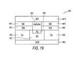
- FIGS. 16-19illustrate a third embodiment of the memory cell 40 .
- FIG. 19illustrates the finished memory cell 40 C
- FIGS. 16-18illustrate the memory cell 40 C at various stages of fabrication.
- the suffix “C”is used in describing this third embodiment for clarity so that similar reference numerals may be used.
- the finished memory cell 40 Cincludes a word line 42 C, which is again referred to as a Metal 1 (M 1 ) layer.
- the word line 42 Chas a layer of conductive material 50 C, such as silver (Ag), disposed thereon.
- a layer of chalcogenide material 52 C, such as germanium selenide (GeSe), having metal ions diffused thereinis disposed over the conductive layer 50 C.
- the layer of conductive material 50 C and the layer of chalcogenide material 52 Care disposed in a window created in a layer of dielectric material 60 C and in a layer of conductive material 44 ′C.
- the layer of conductive material 44 ′Cforms a portion of the digit line and is again referred to as a Metal 2 (M 2 ) layer.
- the other portion of the digit lineis formed by a layer of conductive material 44 ′′C, which is disposed over the chalcogenide layer 52 C and over the Metal 2 layer.
- the layer of conductive material 44 ′′Cis referred to as the Metal 3 (M 3 ) layer.
- Each memory cell 40 Cis typically isolated from adjacent memory cells by oxide regions 54 C, and each memory cell 40 C is typically fabricated on a substrate 56 C.
- FIGS. 16-18One method of fabricating the memory cell 40 C is disclosed with reference to the various stages of fabrication illustrated in FIGS. 16-18 . However, before discussing FIGS. 16-18 , it should be understood that the memory cell 40 C first undergoes the stages of fabrication illustrated in FIGS. 4-6 . Then, as illustrated in FIG. 16 , a layer of dielectric material 60 C is deposited over the structure, and a layer of conductive material 44 ′C (the Metal 2 layer) is deposited over the layer of dielectric material 60 C.
- the layer of dielectric material 60 Cmay be deposited in any suitable manner, such as by chemical vapor deposition, and it may include any suitable dielectric, such as silicon nitride.
- the layer of conductive material 44 ′Cmay be deposited in any suitable manner, such as by sputtering, and it may include any suitable conductive material, such as platinum, aluminum, or tungsten.
- the thickness of the layer of dielectric material 60 Cmay be in the range of 200 A to 1000 A, for example, and the thickness of the layer of conductive material 44 ′C may be in the range of 500 A to 2000 A, for example.
- a window 64is formed in the layer of dielectric material 60 C and in the layer of conductive material 44 ′C to expose at least a portion of the underlying word line 42 C.
- the window 64may be formed in any suitable manner, such as by the use of standard photolithographic techniques.
- a fast ion conductive materialis then disposed on the portion of the word line 42 C exposed by the window 64 .
- the selection of the fast ion conductive material and the manner in which it may be applieddoes not differ from the previous embodiments. Accordingly, for the sake of clarity, in this exemplary embodiment, the base metal of the word line 42 C is selected to be copper, and the more noble metal of the conductive layer 50 C is selected to be silver.
- the structure illustrated in FIG. 16is immersed in the silver immersion solution for a sufficient amount of time to form the layer of conductive material 50 C, as illustrated in FIG. 17 .
- a layer of chalcogenide material 52 Csuch as germanium selenide, may be deposited in the window 64 over the conductive layer 50 C, as illustrated in FIG. 18 .
- the layer of chalcogenide material 52 Cmay be formed by any suitable process, such as chemical vapor deposition.
- the deposited layer of chalcogenide material 52 Cis then planarized, by chemical mechanical planarization for example, so that the layer of chalcogenide material 52 C remains only within the window 64 .
- the thickness of the layer of chalcogenide material 52 Cis approximately the same as the thickness of the layers of dielectric material 60 C and conductive material 44 ′C.
- the structure illustrated in FIG. 18is processed in a manner that causes at least a portion of the material in the conductive layer 50 C to migrate into the layer of chalcogenide material 52 C.
- the structure illustrated in FIG. 18is subjected to ultraviolet radiation and heat to cause silver atoms in the layer of conductive material 50 C to migrate into the layer of chalcogenide material 52 C.
- the layer of chalcogenide material 52 Chas metal ions in it, as illustrated in FIG. 19 .
- a layer of conductive material 44 ′′C(the Metal 3 layer), which forms the remainder of the digit line, may be disposed over the layer of conductive material 44 ′C and over the layer of chalcogenide material 52 C to complete the memory cell 40 C.
- chalcogenide materialis somewhat susceptible to damage from planarization techniques, such as chemical mechanical planarization.
- planarization techniquessuch as chemical mechanical planarization.
- the memory cell 40 Cis relatively immune to any “over planarization” of the chalcogenide material 52 C within the window 64 .
- the planarization stepcan remove some of the relatively delicate chalcogenide material 52 C from the top of the window 64 , the electrical path from the digit line 44 C through the chalcogenide material 52 C typically does not extend directly from the layer of conductive material 44 ′′C. Rather, the shortest path typically extends from the edge of the layer of conductive material 44 ′C.
- the memory cell 40 Ctypically provides for relatively repeatable and consistent memory operation.
Landscapes
- Engineering & Computer Science (AREA)
- Manufacturing & Machinery (AREA)
- Physics & Mathematics (AREA)
- Condensed Matter Physics & Semiconductors (AREA)
- General Physics & Mathematics (AREA)
- Computer Hardware Design (AREA)
- Microelectronics & Electronic Packaging (AREA)
- Power Engineering (AREA)
- Semiconductor Memories (AREA)
Abstract
Description
- 1. Field of the Invention
- The invention relates generally to the field of semiconductor devices and fabrication and, more particularly, to memory elements and methods for making memory elements.
- 2. Background of the Related Art
- This section is intended to introduce the reader to various aspects of art which may be related to various aspects of the present invention that are described and/or claimed below. This discussion is believed to be helpful in providing the reader with background information to facilitate a better understanding of the various aspects of the present invention. Accordingly, it should be understood that these statements are to be read in this light, and not as admissions of prior art.
- Microprocessor-controlled integrated circuits are used in a wide variety of applications. Such applications include personal computers, vehicle control systems, telephone networks, and a host of consumer products. As is well known, microprocessors are essentially generic devices that perform specific functions under the control of a software program. This program is stored in one or more memory devices that are coupled to the microprocessor. Not only does the microprocessor access memory devices to retrieve the program instructions, but it also stores and retrieves data created during execution of the program in one or more memory devices.
- There are a variety of different memory devices available for use in microprocessor-based systems. The type of memory device chosen for a specific function within a microprocessor-based system depends largely upon what features of the memory are best suited to perform the particular function. For instance, volatile memories, such as dynamic random access memories (DRAMs), must be continually powered in order to retain their contents, but they tend to provide greater storage capability and programming options and cycles than non-volatile memories, such as read only memories (ROMs). While non-volatile memories that permit limited reprogramming exist, such as electrically erasable and programmable “ROMs,” all true random access memories, i.e., those memories capable of 1014programming cycles are more, are volatile memories. Although one time programmable read only memories and moderately reprogrammable memories serve many useful applications, a true nonvolatile random access memory (NVRAM) would likely be needed to surpass volatile memories in usefulness.
- Efforts have been underway to create a commercially viable memory device that is both random access and nonvolatile using structure changing memory elements, as opposed to the charge storage memory elements used in most commercial memory devices. The use of electrically writable and erasable phase change materials, i.e., materials which can be electrically switched between generally amorphous and generally crystalline states or between different resistive states while in crystalline form, in memory applications is known in the art and is disclosed, for example, in U.S. Pat. No. 5,296,716 to Ovshinsky et al. The Ovshinsky patent contains a discussion of the general theory of operation of chalcogenide materials, which are a particular type of structure changing material.
- As disclosed in the Ovshinsky patent, such phase change materials can be electrically switched between a first structural state, in which the material is generally amorphous, and a second structural state, in which the material has a generally crystalline local order. The material may also be electrically switched between different detectable states of local order across the entire spectrum between the completely amorphous and the completely crystalline states. In other words, the switching of such materials is not required to take place in a binary fashion between completely amorphous and completely crystalline states. Rather, the material may be switched in incremental steps reflecting changes of local order to provide a “gray scale” represented by a multiplicity of conditions of local order spanning the spectrum from the completely amorphous state to the completely crystalline state.
- These memory elements are monolithic, homogeneous, and formed of chalcogenide material typically selected from the group of Te, Se, Sb, Ni, and Ge. This chalcogenide material exhibits different electrical characteristics depending upon its state. For instance, in its amorphous state the material exhibits a higher resistivity than it does in its crystalline state. Such chalcogenide materials may be switched between numerous electrically detectable conditions of varying resistivity in nanosecond time periods with the input of picojoules of energy. The resulting memory element is truly non-volatile. It will maintain the integrity of the information stored by the memory cell without the need for periodic refresh signals, and the data integrity of the information stored by these memory cells is not lost when power is removed from the device. The memory material is also directly overwritable so that the memory cells need not be erased, i.e., set to a specified starting point, in order to change information stored within the memory cells. Finally, the large dynamic range offered by the memory material theoretically provides for the gray scale storage of multiple bits of binary information in a single cell by mimicking the binary encoded information in analog form and, thereby, storing multiple bits of binary encoded information as a single resistance value in a single cell.
- Traditionally, the operation of chalcogenide memory cells requires that a region of the chalcogenide memory material, called the “active region,” be subjected to a current pulse to change the crystalline state of the chalcogenide material within the active region. Typically, a current density of between about 105and 107amperes/cm2is needed. To obtain this current density in a commercially viable device having at least one million memory cells, for instance, one theory suggests that the active region of each memory cell should be made as small as possible to minimize the total current drawn by the memory device.
- However, such traditional chalcogenide memory cells have evolved into what is referred to as a programmable metallization cell or a plated chalcogenide memory cell for use in a plated chalcogenide random access memory (PCRAM) device. Such a cell includes a chalcogenide material between opposing electrodes. A fast ion conductor material is incorporated into the chalcogenide material. The resistance of such material can be changed between highly resistive and highly conductive states.
- To perform a write operation with the memory cell in its normal high resistive state, a voltage potential is applied to a certain one of the electrodes, with the other of the electrode being held at zero voltage or ground. The electrode having the voltage applied to it functions as an anode, while the electrode held at zero or ground functions as a cathode. The nature of the fast ion conductor material is such that it undergoes a chemical and structural change at a certain applied voltage level. Specifically, at some suitable threshold voltage, the metal ions within the chalcogenide material begin to plate on the cathode and progress through the chalcogenide material toward the anode. The process continues until a conductive dendrite or filament extends between the electrodes, effectively interconnecting the top and bottom electrodes to create an electrical short circuit.
- Once this occurs, dendrite growth stops, and the dendrite is retained when the voltage potentials are removed. This results in the resistance of the chalcogenide material between the electrodes dropping by a factor of about 1,000. The material can be returned to its highly resistive state by reversing the voltage potential between the anode and cathode to cause the dendrite to disappear. Again, the highly resistive state is maintained when the reverse voltage potential is removed. Accordingly, such a device can, for example, function as a reprogrammable memory cell of non-volatile random access memory circuit.
- As mentioned above, the variable resistance material disposed between the electrodes typically is a chalcogenide material having metal ions diffused therein. A specific example is germanium selenide with silver ions. Typically, to provide the silver ions within the germanium selenide material, germanium selenide is deposited onto the first electrode using chemical vapor deposition. A thin layer of silver is then deposited on the glass, for example by physical vapor deposition or another technique. The layer of silver is then irradiated with ultraviolet radiation. The thin nature of the deposited silver allows the energy to pass through the silver to the silver/glass interface to cause the silver to diffuse into the chalcogenide material. The applied energy and overlying silver result in the silver migrating into the glass layer such that a homegenous distribution of silver throughout the layer is ultimately achieved.
- Unfortunately, chalcogenide materials are relatively delicate. The nature of the deposition technique used to deposit the silver can damage the chalcogenide material,and, thus, adversely affect the resulting memory cell. Furthermore, it can be challenging to etch and polish chalcogenide materials. Accordingly, it would be desirable to develop memory cell fabrication methods that avoid steps that can damage such materials.
- The foregoing and other advantages of the invention will become apparent upon reading the following detailed description and upon reference to the drawings in which:
FIG. 1 illustrates a block diagram of an exemplary processor-based device;FIG. 2 illustrates an exemplary memory device;FIG. 3 illustrates a more detailed view of the memory array of the memory device illustrated inFIG. 2 ;FIGS. 4-10 illustrate cross-sectional views of a memory cell during different stages of fabrication;FIGS. 11-15 illustrate cross-sectional views of an alternate embodiment of a memory cell during different stages of fabrication; andFIGS. 16-19 illustrate cross-sectional views of another alternate embodiment of a memory cell during different stages of fabrication.- Specific embodiments of microprocessor-based systems, memories, memory elements, and methods of making such memory elements are described below as they might be implemented for use in semiconductor memory circuits. In the interest of clarity, not all features of an actual implementation are described in this specification. It should be appreciated that in the development of any such actual implementation, as in any engineering project, numerous implementation-specific decisions must be made to achieve the developers' specific goals, such as compliance with system-related and business-related constraints, which may vary from one implementation to another. Moreover, it should be appreciated that such a development effort might be complex and time-consuming, but would nevertheless be a routine undertaking for those of ordinary skill having the benefit of this disclosure.
- Turning now to the drawings, and referring initially to
FIG. 1 , a block diagram depicting an exemplary processor-based device, generally designated by thereference numeral 10, is illustrated. Thedevice 10 may be any of a variety of different types, such as a computer, pager, cellular telephone, personal organizer, control circuit, etc. In a typical processor-based device, one ormore processors 12, such as a microprocessor(s), control many of the functions of thedevice 10. - The
device 10 typically includes apower supply 14. For instance, if thedevice 10 is portable, thepower supply 14 would advantageously include permanent batteries, replaceable batteries, and/or rechargeable batteries. Thepower supply 14 may also include an A/C adapter, so that the device may be plugged into a wall outlet, for instance. In fact, thepower supply 14 may also include a D/C adapter, so that thedevice 10 may be plugged into a vehicle's cigarette lighter, for instance. - Various other devices may be coupled to the processor(s)12, depending upon the functions that the
device 10 performs. For instance, auser interface 16 may be coupled to the processor(s)12. Theuser interface 16 may include an input device, such as buttons, switches, a keyboard, a light pin, a mouse, and/or a voice recognition system, for instance. Adisplay 18 may also be coupled to the processor(s)12. Thedisplay 18 may include an LCD display, a CRT, LEDs, and/or an audio display. Furthermore, an RF subsystem/baseband processor 20 may also be coupled to the processor(s)12. The RF subsystem/baseband processor 20 may include an antenna that is coupled to an RF receiver and to an RF transmitter (not shown). Acommunication port 22 may also be coupled to the processor(s)12. Thecommunication port 22 may be adapted to be coupled to aperipheral device 24, such as a modem, a printer, or a computer, for instance, or to a network, such as a local area network or the Internet. - Because the processor(s)12 controls the functioning of the
device 10 generally under the control of software programming, memory is coupled to the processor(s)12 to store and facilitate execution of the software program. For instance, the processor(s)12 may be coupled tovolatile memory 26, which may include dynamic random access memory (DRAM), static random access memory (SRAM), Double Data Rate (DDR) memory, etc. The processor(s)12 may also be coupled tonon-volatile memory 28. Thenon-volatile memory 28 may include a read only memory (ROM), such as an EPROM or Flash Memory, to be used in conjunction with the volatile memory. The size of the ROM is typically selected to be just large enough to store any necessary operating system, application programs, and fixed data. The volatile memory, on the other hand, is typically quite large so that it can store dynamically loaded applications. Additionally, thenon-volatile memory 28 may include a high capacity memory such as a disk drive, tape drive memory, CD ROM drive, DVD, read/write CD ROM drive, and/or a floppy disk drive. - An exemplary memory device is illustrated in
FIG. 2 and generally designated by areference numeral 30. Thememory device 30 is an integrated circuit memory that is advantageously formed on asemiconductor substrate 32. Thememory device 30 includes a memory matrix orarray 34 that includes a plurality of memory cells for storing data, as described below. Thememory matrix 34 is coupled toperiphery circuitry 36 by the plurality of control lines38. Theperiphery circuitry 36 may include circuitry for addressing the memory cells contained within thememory matrix 34, along with circuitry for storing data in and retrieving data from the memory cells. Theperiphery circuitry 36 may also include other circuitry used for controlling or otherwise insuring the proper functioning of thememory device 30. - A more detailed depiction of the
memory matrix 34 is illustrated inFIG. 3 . As can be seen, thememory matrix 34 includes a plurality ofmemory cells 40 that are arranged in generally perpendicular rows and columns. Thememory cells 40 in each row are coupled together by arespective word line 42, and thememory cells 40 in each column are coupled together by arespective digit line 44. Specifically, eachmemory cell 40 includes aword line node 46 that is coupled to arespective word line 42, and eachmemory cell 40 includes adigit line node 48 that is coupled to arespective digit line 44. The conductive word lines42 anddigit lines 44 are collectively referred to as address lines. These address lines are electrically coupled to theperiphery circuitry 36 so that each of thememory cells 40 can be accessed for the storage and retrieval of information. - Turning now to
FIGS. 4-10 , a first exemplary embodiment of a memory cell49 will be described.FIG. 10 illustrates thefinished memory cell 40A, andFIGS. 4-9 illustrate thememory cell 40A at various stages of fabrication. The suffix “A” is used in describing this first embodiment for clarity so that similar reference numerals may be used to describe subsequent embodiments. As illustrated inFIG. 10 , thefinished memory cell 40A includes aword line 42A, which is often referred to as a Metal1 (M1) layer. Theword line 42A has a layer ofconductive material 50A, such as silver (Ag), disposed thereon. A layer ofchalcogenide material 52A, such as germanium selenide (GeSe), having metal ions diffused therein is disposed over theconductive layer 50A. The metal ions diffused in thechalcogenide material 52A typically originate in the layer ofconductive material 50A. Thedigit line 44A, often referred to as a Metal2 (M2) layer, is disposed over thechalcogenide layer 52A. Eachmemory cell 40A is typically isolated from adjacent memory cells byoxide regions 54A, and eachmemory cell 40A is typically fabricated on asubstrate 56A. - One method of fabricating the
memory cell 40A is disclosed with reference to the various stages of fabrication illustrated inFIGS. 4-9 . Referring first toFIG. 4 , asubstrate 56A is typically used as a base upon which thememory cells 40A of thememory array 44 are formed. In this discussion, thesubstrate 56A is generally used in a generic sense, because it is possible for thesubstrate 56A to take various forms depending upon the nature of the circuit design. For example, thesubstrate 56A may be a suitable semiconductor substrate, such as silicon or galium arsenide, or a suitable dielectric substrate, such as PECVD silicon dioxide. Furthermore, thesubstrate 56A may include layers, devices, and/or structures upon which or around which thememory cells 40A may be fabricated. - A layer of
dielectric material 54A, for example an oxide such as silicon dioxide, is formed over thesubstrate 56A, as illustrated inFIG. 5 . The layer ofdielectric material 54A may be formed by any suitable process, such as by chemical vapor deposition. Awindow 58A is formed in the layer ofdielectric material 54A. The window may extend partially through the layer ofdielectric material 54A, or completely through the layer ofdielectric material 54A to thesubstrate 56A, as illustrated inFIG. 5 . Thewindow 58A may be formed by any suitable process, such as by the use of standard photolithographic techniques. - As illustrated in
FIGS. 5 and 6 , a layer of conductive material is deposited into thewindow 58A and planarized to form theword line 42A. Again, any suitable deposition technique, such as sputtering, and any suitable planarization technique, such as chemical mechanical planarization (CMP), may be used. The conductive material used to form theword line 42A is typically a metal, such as copper, tungsten, nickel, or aluminum. Although theword line 42A is illustrated as being formed in adielectric material 54A in this embodiment, it should be appreciated that theword line 42A may be formed in other manners as well. For example, theword line 42A may be buried in thesubstrate 56A. - A fast ion conductive material is then disposed on the
word line 42A. The fast ion conductive material is selected to cooperate with a subsequently applied layer of chalcogenide material to form the memory element of thememory cell 40A. In this embodiment, theword line 42A is plated with theconductive material 50A using an immersion plating process. In general, immersion plating replaces a less noble metal with a more noble metal. It is an ion exchange process that requires neither external electricity nor a catalyst. Immersion plating can be used in a self-limiting process, and it usually plates thinner films than other plating methods. Immersion plating depends on the base metal, i.e., the less noble metal. Many factors can influence immersion plating, such as the type of ligand used to take up the base metal and to keep the base metal in solution. - In this exemplary embodiment, the base metal of the
word line 42A is selected to be copper, and the more noble metal of theconductive layer 50A is selected to be silver. Of course, it should be recognized that other base metals, such as nickel, aluminum, or tungsten, for example, may be used in place of copper, and that alloys of such metals may be used as well. In addition, various “more noble” metals, such as gold, may be used in place of silver. However, for the purposes of this exemplary embodiment utilizing copper and silver, a silver immersion solution called “argentomerse” available from Technic, Inc. may be used. This silver immersion solution utilizes a cyanide salt chemistry, which essentially represents a general purpose immersion plating solution. A silver immersion solution such as argentomerse should suffice for plating silver on base metals such as nickel or copper. However, for immersion plating of silver on tungsten, it may be desirable to utilize another silver immersion solution in order to optimize the chemistry. The structure illustrated inFIG. 6 is immersed in the silver immersion solution for a sufficient amount of time to form the layer ofconductive material 50A For example, the structure may be immersed in the solution for 15 to 30 minutes to form the conductive layer5A having a thickness of 500 A to 2000 A. - After the
conductive layer 50A has been formed on theword line 42A, a layer ofchalcogenide material 52A, such as germanium selenide, may be formed over theconductive layer 50A, as illustrated inFIG. 8 . The layer ofchalcogenide material 52A may be formed by any suitable process, such as chemical vapor deposition. The layer ofchalcogenide material 52A may have a thickness in the range of 200 A to 800 A, for example. - Once the layer of
chalcogenide material 52A is formed over the layer ofconductive material 50A, the structure illustrated inFIG. 8 is processed in a manner that causes at least a portion of the material in theconductive layer 50A to migrate into the layer ofchalcogenide material 52A. In this embodiment, the structure illustrated inFIG. 8 is subjected to ultraviolet radiation and heat to cause silver atoms in the layer ofconductive material 50A to migrate into the layer ofchalcogenide material 52A. For example, the structure inFIG. 8 may be submitted to ultraviolet radiation in the range of 160 nm to 904 nm, e.g., 405 nm, at an intensity of 10 microjoules to 10 millijoules for a period of 5 to 30 minutes, and heat at a temperature of 50 to 85 degrees Celsius for a period of 5 to 20 minutes. Typically, the heat cycle is performed first, followed by the UV cycle. - After this conversion process, the layer of
chalcogenide material 52A has metal ions in it, as illustrated inFIG. 9 . Then, the Metal2 (M2) layer, which forms thedigit line 44A, may be disposed over the layer ofchalcogenide material 52A, as illustrated inFIG. 10 , to complete thememory cell 40A. - It should be appreciated from the discussion of the structure and method of fabrication of the
memory cell 40A that it represents an inverted PCRAM memory cell. As discussed previously, a typical PCRAM memory cell is fabricated by forming a layer of chalcogenide material on the Metal1 layer, thus requiring the conductive layer, such as silver, to be disposed on the chalcogenide layer. However, because chalcogenide is a very delicate material as discussed previously, known methods of depositing silver on chalcogenide are difficult to control in a reliable and repeatable fashion. However, by inverting the traditional PCRAM memory cell so that the conductive layer, such as silver, is disposed on the Metal1 layer, the delicate nature of the subsequently deposited chalcogenide material does not pose a problem. FIGS. 11-15 illustrate a second embodiment of thememory cell 40.FIG. 15 illustrates thefinished memory cell 40B, andFIGS. 11-14 illustrate thememory cell 40B at various stages of fabrication. The suffix “B” is used in describing this second embodiment for clarity so that similar reference numerals may be used. As illustrated inFIG. 15 , thefinished memory cell 40B includes aword line 42B, which is again referred to as a Metal1 (M1) layer. Theword line 42B has a layer ofconductive material 50B, such as silver (Ag), disposed thereon. A layer ofchalcogenide material 52B, such as germanium selenide (GeSe), having metal ions diffused therein is disposed over theconductive layer 50B. Unlike the first embodiment, the layer ofconductive material 50B and the layer ofchalcogenide material 52B are disposed in a window created in a layer ofdielectric material 60B. Thedigit line 44B, again referred to as a Metal2 (M2) layer, is disposed over thechalcogenide layer 52B. Eachmemory cell 40B is typically isolated from adjacent memory cells byoxide regions 54B, and eachmemory cell 40B is typically fabricated on asubstrate 56B.- One method of fabricating the
memory cell 40B is disclosed with reference to, the various stages of fabrication illustrated inFIGS. 11-14 . However, before discussingFIGS. 11-14 , it should be understood that thememory cell 40B first undergoes the stages of fabrication illustrated inFIGS. 4-6 . Then, as illustrated inFIG. 11 , a layer ofdielectric material 60B is deposited over the structure, and awindow 62 is formed in the layer ofdielectric material 60B to expose at least a portion of theunderlying word line 42B. The layer ofdielectric material 60B may be deposited in any suitable manner, such as by chemical vapor deposition, and it may include any suitable dielectric, such as silicon nitride. The thickness of the layer ofdielectric material 60B may be in the range of 200 A to 1000 A, for example. - A fast ion conductive material is then disposed on the portion of the
word line 42B exposed by thewindow 62. The selection of the fast ion conductive material and the manner in which it may be applied does not differ from the previous embodiment. Accordingly, for the sake of clarity, in this exemplary embodiment, the base metal of theword line 42B is selected to be copper, and the more noble metal of theconductive layer 50B is selected to be silver. The structure illustrated inFIG. 11 is immersed in the silver immersion solution for a sufficient amount of time to form the layer ofconductive material 50B, as illustrated inFIG. 12 . - After the
conductive layer 50B has been formed on theword line 42B, a layer ofchalcogenide material 52B, such as germanium selenide, may be deposited in thewindow 62 over theconductive layer 50B, as illustrated inFIG. 13 . The layer ofchalcogenide material 52B may be formed by any suitable process, such as chemical vapor deposition. The deposited layer ofchalcogenide material 52B is then planarized, by chemical mechanical planarizatiqn for example, so that the layer ofchalcogenide material 52B remains only within thewindow 62. Thus, the thickness of the layer ofchalcogenide material 52B is approximately the same as the thickness of the layer ofdielectric material 60B. - Once the layer of
chalcogenide material 52B is formed in thewindow 62, the structure illustrated inFIG. 13 is processed in a manner that causes at least a portion of the material in theconductive layer 50B to migrate into the layer ofchalcogenide material 52B. As in the previous embodiment, the structure illustrated inFIG. 13 is subjected to ultraviolet radiation and heat to cause silver atoms in the layer ofconductive material 50B to migrate into the layer ofchalcogenide material 52B. - After this conversion process, the layer of
chalcogenide material 52B has metal ions in it, as illustrated inFIG. 14 . Then, the Metal2 (M2) layer, which forms thedigit line 44B, may be disposed over the layer ofdielectric material 60B and over the layer ofchalcogenide material 52B, as illustrated inFIG. 15 , to complete thememory cell 40B. FIGS. 16-19 illustrate a third embodiment of thememory cell 40.FIG. 19 illustrates thefinished memory cell 40C, andFIGS. 16-18 illustrate thememory cell 40C at various stages of fabrication. The suffix “C” is used in describing this third embodiment for clarity so that similar reference numerals may be used. As illustrated inFIG. 19 , thefinished memory cell 40C includes aword line 42C, which is again referred to as a Metal1 (M1) layer. Theword line 42C has a layer ofconductive material 50C, such as silver (Ag), disposed thereon. A layer ofchalcogenide material 52C, such as germanium selenide (GeSe), having metal ions diffused therein is disposed over theconductive layer 50C. Unlike the previous embodiments, the layer ofconductive material 50C and the layer ofchalcogenide material 52C are disposed in a window created in a layer ofdielectric material 60C and in a layer ofconductive material 44′C. The layer ofconductive material 44′C forms a portion of the digit line and is again referred to as a Metal2 (M2) layer. The other portion of the digit line is formed by a layer ofconductive material 44″C, which is disposed over thechalcogenide layer 52C and over the Metal2 layer. The layer ofconductive material 44″C is referred to as the Metal3 (M3) layer. Eachmemory cell 40C is typically isolated from adjacent memory cells byoxide regions 54C, and eachmemory cell 40C is typically fabricated on asubstrate 56C.- One method of fabricating the
memory cell 40C is disclosed with reference to the various stages of fabrication illustrated inFIGS. 16-18 . However, before discussingFIGS. 16-18 , it should be understood that thememory cell 40C first undergoes the stages of fabrication illustrated inFIGS. 4-6 . Then, as illustrated inFIG. 16 , a layer ofdielectric material 60C is deposited over the structure, and a layer ofconductive material 44′C (the Metal2 layer) is deposited over the layer ofdielectric material 60C. The layer ofdielectric material 60C may be deposited in any suitable manner, such as by chemical vapor deposition, and it may include any suitable dielectric, such as silicon nitride. The layer ofconductive material 44′C may be deposited in any suitable manner, such as by sputtering, and it may include any suitable conductive material, such as platinum, aluminum, or tungsten. The thickness of the layer ofdielectric material 60C may be in the range of 200 A to 1000 A, for example, and the thickness of the layer ofconductive material 44′C may be in the range of 500 A to 2000 A, for example. - A
window 64 is formed in the layer ofdielectric material 60C and in the layer ofconductive material 44′C to expose at least a portion of theunderlying word line 42C. Thewindow 64 may be formed in any suitable manner, such as by the use of standard photolithographic techniques. - A fast ion conductive material is then disposed on the portion of the
word line 42C exposed by thewindow 64. The selection of the fast ion conductive material and the manner in which it may be applied does not differ from the previous embodiments. Accordingly, for the sake of clarity, in this exemplary embodiment, the base metal of theword line 42C is selected to be copper, and the more noble metal of theconductive layer 50C is selected to be silver. The structure illustrated inFIG. 16 is immersed in the silver immersion solution for a sufficient amount of time to form the layer ofconductive material 50C, as illustrated inFIG. 17 . - After the
conductive layer 50C has been formed on theword line 42C, a layer ofchalcogenide material 52C, such as germanium selenide, may be deposited in thewindow 64 over theconductive layer 50C, as illustrated inFIG. 18 . The layer ofchalcogenide material 52C may be formed by any suitable process, such as chemical vapor deposition. The deposited layer ofchalcogenide material 52C is then planarized, by chemical mechanical planarization for example, so that the layer ofchalcogenide material 52C remains only within thewindow 64. Thus, the thickness of the layer ofchalcogenide material 52C is approximately the same as the thickness of the layers ofdielectric material 60C andconductive material 44′C. - Once the layer of
chalcogenide material 52C is formed in thewindow 64, the structure illustrated inFIG. 18 is processed in a manner that causes at least a portion of the material in theconductive layer 50C to migrate into the layer ofchalcogenide material 52C. As in the previous embodiments, the structure illustrated inFIG. 18 is subjected to ultraviolet radiation and heat to cause silver atoms in the layer ofconductive material 50C to migrate into the layer ofchalcogenide material 52C. - After this conversion process, the layer of
chalcogenide material 52C has metal ions in it, as illustrated inFIG. 19 . Then, a layer ofconductive material 44″C (the Metal3 layer), which forms the remainder of the digit line, may be disposed over the layer ofconductive material 44′C and over the layer ofchalcogenide material 52C to complete thememory cell 40C. - As previously mention, chalcogenide material is somewhat susceptible to damage from planarization techniques, such as chemical mechanical planarization. However, it should be noted that the
memory cell 40C is relatively immune to any “over planarization” of thechalcogenide material 52C within thewindow 64. Although the planarization step can remove some of the relatively delicatechalcogenide material 52C from the top of thewindow 64, the electrical path from the digit line44C through thechalcogenide material 52C typically does not extend directly from the layer ofconductive material 44″C. Rather, the shortest path typically extends from the edge of the layer ofconductive material 44′C. Thus, for over planarization to affect thememory cell 40C adversely,chalcogenide material 52C below the level of thedielectric layer 60C would have to be removed. Since over planarization to such an extent is unlikely, thememory cell 40C typically provides for relatively repeatable and consistent memory operation. - While the invention may be susceptible to various modifications and alternative forms, specific embodiments have been shown by way of example in the drawings and have been described in detail herein. However, it should be understood that the invention is not intended to be limited to the particular forms disclosed. Rather, the invention is to cover all modifications, equivalents, and alternatives falling within the spirit and scope of the invention as defined by the following appended claims.
Claims (19)
Priority Applications (1)
| Application Number | Priority Date | Filing Date | Title |
|---|---|---|---|
| US11/751,896US7687793B2 (en) | 2001-05-11 | 2007-05-22 | Resistance variable memory cells |
Applications Claiming Priority (4)
| Application Number | Priority Date | Filing Date | Title |
|---|---|---|---|
| US09/853,233US7102150B2 (en) | 2001-05-11 | 2001-05-11 | PCRAM memory cell and method of making same |
| US10/205,387US7071021B2 (en) | 2001-05-11 | 2002-07-25 | PCRAM memory cell and method of making same |
| US11/302,119US7235419B2 (en) | 2001-05-11 | 2005-12-14 | Method of making a memory cell |
| US11/751,896US7687793B2 (en) | 2001-05-11 | 2007-05-22 | Resistance variable memory cells |
Related Parent Applications (1)
| Application Number | Title | Priority Date | Filing Date |
|---|---|---|---|
| US11/302,119ContinuationUS7235419B2 (en) | 2001-05-11 | 2005-12-14 | Method of making a memory cell |
Publications (2)
| Publication Number | Publication Date |
|---|---|
| US20070235712A1true US20070235712A1 (en) | 2007-10-11 |
| US7687793B2 US7687793B2 (en) | 2010-03-30 |
Family
ID=25315450
Family Applications (4)
| Application Number | Title | Priority Date | Filing Date |
|---|---|---|---|
| US09/853,233Expired - LifetimeUS7102150B2 (en) | 2001-05-11 | 2001-05-11 | PCRAM memory cell and method of making same |
| US10/205,387Expired - Fee RelatedUS7071021B2 (en) | 2001-05-11 | 2002-07-25 | PCRAM memory cell and method of making same |
| US11/302,119Expired - LifetimeUS7235419B2 (en) | 2001-05-11 | 2005-12-14 | Method of making a memory cell |
| US11/751,896Expired - Fee RelatedUS7687793B2 (en) | 2001-05-11 | 2007-05-22 | Resistance variable memory cells |
Family Applications Before (3)
| Application Number | Title | Priority Date | Filing Date |
|---|---|---|---|
| US09/853,233Expired - LifetimeUS7102150B2 (en) | 2001-05-11 | 2001-05-11 | PCRAM memory cell and method of making same |
| US10/205,387Expired - Fee RelatedUS7071021B2 (en) | 2001-05-11 | 2002-07-25 | PCRAM memory cell and method of making same |
| US11/302,119Expired - LifetimeUS7235419B2 (en) | 2001-05-11 | 2005-12-14 | Method of making a memory cell |
Country Status (1)
| Country | Link |
|---|---|
| US (4) | US7102150B2 (en) |
Cited By (5)
| Publication number | Priority date | Publication date | Assignee | Title |
|---|---|---|---|---|
| US20050174861A1 (en)* | 2004-01-05 | 2005-08-11 | Young-Tae Kim | Phase-change memory device and method of manufacturing the same |
| US7491573B1 (en) | 2008-03-13 | 2009-02-17 | International Business Machines Corporation | Phase change materials for applications that require fast switching and high endurance |
| US20120015475A1 (en)* | 2010-07-14 | 2012-01-19 | Jun Liu | Methods Of Forming Memory Cells, And Methods Of Patterning Chalcogenide-Containing Stacks |
| US20130026436A1 (en)* | 2011-07-27 | 2013-01-31 | International Business Machines Corporation | Phase change memory electrode with sheath for reduced programming current |
| WO2013169758A1 (en)* | 2012-05-07 | 2013-11-14 | Micron Technology, Inc. | Resistive memory having confined filament formation |
Families Citing this family (206)
| Publication number | Priority date | Publication date | Assignee | Title |
|---|---|---|---|---|
| US5841768A (en)* | 1996-06-27 | 1998-11-24 | Interdigital Technology Corporation | Method of controlling initial power ramp-up in CDMA systems by using short codes |
| US7902536B2 (en)* | 1999-03-25 | 2011-03-08 | Ovonyx, Inc. | Memory device and method of making same |
| US6734455B2 (en) | 2001-03-15 | 2004-05-11 | Micron Technology, Inc. | Agglomeration elimination for metal sputter deposition of chalcogenides |
| US7102150B2 (en) | 2001-05-11 | 2006-09-05 | Harshfield Steven T | PCRAM memory cell and method of making same |
| US6951805B2 (en) | 2001-08-01 | 2005-10-04 | Micron Technology, Inc. | Method of forming integrated circuitry, method of forming memory circuitry, and method of forming random access memory circuitry |
| US6881623B2 (en) | 2001-08-29 | 2005-04-19 | Micron Technology, Inc. | Method of forming chalcogenide comprising devices, method of forming a programmable memory cell of memory circuitry, and a chalcogenide comprising device |
| US6955940B2 (en) | 2001-08-29 | 2005-10-18 | Micron Technology, Inc. | Method of forming chalcogenide comprising devices |
| US6784018B2 (en) | 2001-08-29 | 2004-08-31 | Micron Technology, Inc. | Method of forming chalcogenide comprising devices and method of forming a programmable memory cell of memory circuitry |
| US6800899B2 (en)* | 2001-08-30 | 2004-10-05 | Micron Technology, Inc. | Vertical transistors, electrical devices containing a vertical transistor, and computer systems containing a vertical transistor |
| US6646902B2 (en) | 2001-08-30 | 2003-11-11 | Micron Technology, Inc. | Method of retaining memory state in a programmable conductor RAM |
| US7109056B2 (en)* | 2001-09-20 | 2006-09-19 | Micron Technology, Inc. | Electro-and electroless plating of metal in the manufacture of PCRAM devices |
| US6815818B2 (en) | 2001-11-19 | 2004-11-09 | Micron Technology, Inc. | Electrode structure for use in an integrated circuit |
| US6791859B2 (en) | 2001-11-20 | 2004-09-14 | Micron Technology, Inc. | Complementary bit PCRAM sense amplifier and method of operation |
| US6909656B2 (en)* | 2002-01-04 | 2005-06-21 | Micron Technology, Inc. | PCRAM rewrite prevention |
| US6867064B2 (en) | 2002-02-15 | 2005-03-15 | Micron Technology, Inc. | Method to alter chalcogenide glass for improved switching characteristics |
| US6791885B2 (en) | 2002-02-19 | 2004-09-14 | Micron Technology, Inc. | Programmable conductor random access memory and method for sensing same |
| US6809362B2 (en) | 2002-02-20 | 2004-10-26 | Micron Technology, Inc. | Multiple data state memory cell |
| US7087919B2 (en) | 2002-02-20 | 2006-08-08 | Micron Technology, Inc. | Layered resistance variable memory device and method of fabrication |
| US7151273B2 (en) | 2002-02-20 | 2006-12-19 | Micron Technology, Inc. | Silver-selenide/chalcogenide glass stack for resistance variable memory |
| US6847535B2 (en) | 2002-02-20 | 2005-01-25 | Micron Technology, Inc. | Removable programmable conductor memory card and associated read/write device and method of operation |
| US6937528B2 (en) | 2002-03-05 | 2005-08-30 | Micron Technology, Inc. | Variable resistance memory and method for sensing same |
| US6849868B2 (en) | 2002-03-14 | 2005-02-01 | Micron Technology, Inc. | Methods and apparatus for resistance variable material cells |
| US6858482B2 (en) | 2002-04-10 | 2005-02-22 | Micron Technology, Inc. | Method of manufacture of programmable switching circuits and memory cells employing a glass layer |
| US6864500B2 (en)* | 2002-04-10 | 2005-03-08 | Micron Technology, Inc. | Programmable conductor memory cell structure |
| US6855975B2 (en) | 2002-04-10 | 2005-02-15 | Micron Technology, Inc. | Thin film diode integrated with chalcogenide memory cell |
| US6731528B2 (en)* | 2002-05-03 | 2004-05-04 | Micron Technology, Inc. | Dual write cycle programmable conductor memory system and method of operation |
| US6825135B2 (en) | 2002-06-06 | 2004-11-30 | Micron Technology, Inc. | Elimination of dendrite formation during metal/chalcogenide glass deposition |
| US6890790B2 (en)* | 2002-06-06 | 2005-05-10 | Micron Technology, Inc. | Co-sputter deposition of metal-doped chalcogenides |
| US7015494B2 (en) | 2002-07-10 | 2006-03-21 | Micron Technology, Inc. | Assemblies displaying differential negative resistance |
| TWI233204B (en)* | 2002-07-26 | 2005-05-21 | Infineon Technologies Ag | Nonvolatile memory element and associated production methods and memory element arrangements |
| US7209378B2 (en) | 2002-08-08 | 2007-04-24 | Micron Technology, Inc. | Columnar 1T-N memory cell structure |
| US7018863B2 (en)* | 2002-08-22 | 2006-03-28 | Micron Technology, Inc. | Method of manufacture of a resistance variable memory cell |
| US6867114B2 (en) | 2002-08-29 | 2005-03-15 | Micron Technology Inc. | Methods to form a memory cell with metal-rich metal chalcogenide |
| US6831019B1 (en) | 2002-08-29 | 2004-12-14 | Micron Technology, Inc. | Plasma etching methods and methods of forming memory devices comprising a chalcogenide comprising layer received operably proximate conductive electrodes |
| US6864521B2 (en) | 2002-08-29 | 2005-03-08 | Micron Technology, Inc. | Method to control silver concentration in a resistance variable memory element |
| US7010644B2 (en) | 2002-08-29 | 2006-03-07 | Micron Technology, Inc. | Software refreshed memory device and method |
| US7364644B2 (en) | 2002-08-29 | 2008-04-29 | Micron Technology, Inc. | Silver selenide film stoichiometry and morphology control in sputter deposition |
| US7294527B2 (en) | 2002-08-29 | 2007-11-13 | Micron Technology Inc. | Method of forming a memory cell |
| US7163837B2 (en) | 2002-08-29 | 2007-01-16 | Micron Technology, Inc. | Method of forming a resistance variable memory element |
| US7022579B2 (en) | 2003-03-14 | 2006-04-04 | Micron Technology, Inc. | Method for filling via with metal |
| TWI245288B (en)* | 2003-03-20 | 2005-12-11 | Sony Corp | Semiconductor memory element and semiconductor memory device using the same |
| US6930909B2 (en) | 2003-06-25 | 2005-08-16 | Micron Technology, Inc. | Memory device and methods of controlling resistance variation and resistance profile drift |
| US6961277B2 (en) | 2003-07-08 | 2005-11-01 | Micron Technology, Inc. | Method of refreshing a PCRAM memory device |
| US7061004B2 (en) | 2003-07-21 | 2006-06-13 | Micron Technology, Inc. | Resistance variable memory elements and methods of formation |
| DE10342026A1 (en)* | 2003-09-11 | 2005-04-28 | Infineon Technologies Ag | Memory cell with ion conduction storage mechanism and method for its production |
| US6903361B2 (en) | 2003-09-17 | 2005-06-07 | Micron Technology, Inc. | Non-volatile memory structure |
| US7050319B2 (en)* | 2003-12-03 | 2006-05-23 | Micron Technology, Inc. | Memory architecture and method of manufacture and operation thereof |
| US7138687B2 (en)* | 2004-01-26 | 2006-11-21 | Macronix International Co., Ltd. | Thin film phase-change memory |
| US7098068B2 (en) | 2004-03-10 | 2006-08-29 | Micron Technology, Inc. | Method of forming a chalcogenide material containing device |
| US7583551B2 (en) | 2004-03-10 | 2009-09-01 | Micron Technology, Inc. | Power management control and controlling memory refresh operations |
| US20050260338A1 (en)* | 2004-05-19 | 2005-11-24 | Trendon Touch Technology Corp. | Method of manufacturing circuit layout on touch panel by utilizing metal plating technology |
| US7190048B2 (en) | 2004-07-19 | 2007-03-13 | Micron Technology, Inc. | Resistance variable memory device and method of fabrication |
| US7326950B2 (en) | 2004-07-19 | 2008-02-05 | Micron Technology, Inc. | Memory device with switching glass layer |
| US7354793B2 (en) | 2004-08-12 | 2008-04-08 | Micron Technology, Inc. | Method of forming a PCRAM device incorporating a resistance-variable chalocogenide element |
| US7365411B2 (en) | 2004-08-12 | 2008-04-29 | Micron Technology, Inc. | Resistance variable memory with temperature tolerant materials |
| US7151688B2 (en) | 2004-09-01 | 2006-12-19 | Micron Technology, Inc. | Sensing of resistance variable memory devices |
| US7224598B2 (en)* | 2004-09-02 | 2007-05-29 | Hewlett-Packard Development Company, L.P. | Programming of programmable resistive memory devices |
| US7189626B2 (en)* | 2004-11-03 | 2007-03-13 | Micron Technology, Inc. | Electroless plating of metal caps for chalcogenide-based memory devices |
| US20060131555A1 (en)* | 2004-12-22 | 2006-06-22 | Micron Technology, Inc. | Resistance variable devices with controllable channels |
| US7374174B2 (en) | 2004-12-22 | 2008-05-20 | Micron Technology, Inc. | Small electrode for resistance variable devices |
| FR2880177B1 (en)* | 2004-12-23 | 2007-05-18 | Commissariat Energie Atomique | MEMORY PMC HAVING IMPROVED RETENTION TIME AND WRITING SPEED |
| US7361925B2 (en)* | 2005-02-10 | 2008-04-22 | Infineon Technologies Ag | Integrated circuit having a memory including a low-k dielectric material for thermal isolation |
| US7317200B2 (en) | 2005-02-23 | 2008-01-08 | Micron Technology, Inc. | SnSe-based limited reprogrammable cell |
| DE102005012047A1 (en)* | 2005-03-16 | 2006-09-28 | Infineon Technologies Ag | Solid-state electrolyte memory manufacture involves coating first electrode with solid-state electrolyte layer, and then forming second electrode on solid-state electrolyte layer |
| US7427770B2 (en) | 2005-04-22 | 2008-09-23 | Micron Technology, Inc. | Memory array for increased bit density |
| US7269044B2 (en) | 2005-04-22 | 2007-09-11 | Micron Technology, Inc. | Method and apparatus for accessing a memory array |
| US7709289B2 (en) | 2005-04-22 | 2010-05-04 | Micron Technology, Inc. | Memory elements having patterned electrodes and method of forming the same |
| US7269079B2 (en) | 2005-05-16 | 2007-09-11 | Micron Technology, Inc. | Power circuits for reducing a number of power supply voltage taps required for sensing a resistive memory |
| US7233520B2 (en) | 2005-07-08 | 2007-06-19 | Micron Technology, Inc. | Process for erasing chalcogenide variable resistance memory bits |
| US7274034B2 (en) | 2005-08-01 | 2007-09-25 | Micron Technology, Inc. | Resistance variable memory device with sputtered metal-chalcogenide region and method of fabrication |
| US7317567B2 (en) | 2005-08-02 | 2008-01-08 | Micron Technology, Inc. | Method and apparatus for providing color changing thin film material |
| US7332735B2 (en) | 2005-08-02 | 2008-02-19 | Micron Technology, Inc. | Phase change memory cell and method of formation |
| US7579615B2 (en) | 2005-08-09 | 2009-08-25 | Micron Technology, Inc. | Access transistor for memory device |
| US7304368B2 (en) | 2005-08-11 | 2007-12-04 | Micron Technology, Inc. | Chalcogenide-based electrokinetic memory element and method of forming the same |
| US7251154B2 (en) | 2005-08-15 | 2007-07-31 | Micron Technology, Inc. | Method and apparatus providing a cross-point memory array using a variable resistance memory cell and capacitance |
| US7277313B2 (en) | 2005-08-31 | 2007-10-02 | Micron Technology, Inc. | Resistance variable memory element with threshold device and method of forming the same |
| US7635855B2 (en) | 2005-11-15 | 2009-12-22 | Macronix International Co., Ltd. | I-shaped phase change memory cell |
| US7449710B2 (en) | 2005-11-21 | 2008-11-11 | Macronix International Co., Ltd. | Vacuum jacket for phase change memory element |
| US7875871B2 (en) | 2006-03-31 | 2011-01-25 | Sandisk 3D Llc | Heterojunction device comprising a semiconductor and a resistivity-switching oxide or nitride |
| KR100729361B1 (en)* | 2006-04-24 | 2007-06-15 | 삼성전자주식회사 | Gap fill method and method for forming semiconductor memory device using the same |
| US7501648B2 (en)* | 2006-08-16 | 2009-03-10 | International Business Machines Corporation | Phase change materials and associated memory devices |
| US7560723B2 (en) | 2006-08-29 | 2009-07-14 | Micron Technology, Inc. | Enhanced memory density resistance variable memory cells, arrays, devices and systems including the same, and methods of fabrication |
| US8003972B2 (en) | 2006-08-30 | 2011-08-23 | Micron Technology, Inc. | Bottom electrode geometry for phase change memory |
| US7511984B2 (en)* | 2006-08-30 | 2009-03-31 | Micron Technology, Inc. | Phase change memory |
| US8232175B2 (en)* | 2006-09-14 | 2012-07-31 | Spansion Llc | Damascene metal-insulator-metal (MIM) device with improved scaleability |
| WO2008088599A2 (en)* | 2006-10-19 | 2008-07-24 | Boise State University | Forced ion migration for chalcogenide phase change memory device |
| US7718989B2 (en) | 2006-12-28 | 2010-05-18 | Macronix International Co., Ltd. | Resistor random access memory cell device |
| US7663135B2 (en) | 2007-01-31 | 2010-02-16 | Macronix International Co., Ltd. | Memory cell having a side electrode contact |
| US7800093B2 (en)* | 2007-02-01 | 2010-09-21 | Qimonda North America Corp. | Resistive memory including buried word lines |
| US7718533B2 (en)* | 2007-05-08 | 2010-05-18 | Micron Technology, Inc. | Inverted variable resistance memory cell and method of making the same |
| US20080278988A1 (en)* | 2007-05-09 | 2008-11-13 | Klaus Ufert | Resistive switching element |
| KR100881055B1 (en)* | 2007-06-20 | 2009-01-30 | 삼성전자주식회사 | Phase change memory unit, manufacturing method thereof, phase change memory device including same and manufacturing method thereof |
| US7813167B2 (en) | 2008-03-21 | 2010-10-12 | Micron Technology, Inc. | Memory cell |
| US8233308B2 (en) | 2007-06-29 | 2012-07-31 | Sandisk 3D Llc | Memory cell that employs a selectively deposited reversible resistance-switching element and methods of forming the same |
| US7824956B2 (en) | 2007-06-29 | 2010-11-02 | Sandisk 3D Llc | Memory cell that employs a selectively grown reversible resistance-switching element and methods of forming the same |
| US20090104756A1 (en)* | 2007-06-29 | 2009-04-23 | Tanmay Kumar | Method to form a rewriteable memory cell comprising a diode and a resistivity-switching grown oxide |
| KR101447176B1 (en)* | 2007-06-29 | 2014-10-08 | 쌘디스크 3디 엘엘씨 | Method for forming a memory cell and a memory cell using a selectively reversible resistive-switching element |
| US7884342B2 (en)* | 2007-07-31 | 2011-02-08 | Macronix International Co., Ltd. | Phase change memory bridge cell |
| US7729161B2 (en)* | 2007-08-02 | 2010-06-01 | Macronix International Co., Ltd. | Phase change memory with dual word lines and source lines and method of operating same |
| FR2922368A1 (en)* | 2007-10-16 | 2009-04-17 | Commissariat Energie Atomique | METHOD FOR MANUFACTURING A CBRAM MEMORY HAVING IMPROVED RELIABILITY |
| US7989793B2 (en)* | 2007-12-10 | 2011-08-02 | Electronics And Telecommunications Research Institute | Electrical device using phase change material, phase change memory device using solid state reaction and method for fabricating the same |
| US7768812B2 (en) | 2008-01-15 | 2010-08-03 | Micron Technology, Inc. | Memory cells, memory cell programming methods, memory cell reading methods, memory cell operating methods, and memory devices |
| US8168468B2 (en)* | 2008-02-29 | 2012-05-01 | Freescale Semiconductor, Inc. | Method of making a semiconductor device including a bridgeable material |
| US8034655B2 (en)* | 2008-04-08 | 2011-10-11 | Micron Technology, Inc. | Non-volatile resistive oxide memory cells, non-volatile resistive oxide memory arrays, and methods of forming non-volatile resistive oxide memory cells and memory arrays |
| US8211743B2 (en)* | 2008-05-02 | 2012-07-03 | Micron Technology, Inc. | Methods of forming non-volatile memory cells having multi-resistive state material between conductive electrodes |
| US8114468B2 (en) | 2008-06-18 | 2012-02-14 | Boise Technology, Inc. | Methods of forming a non-volatile resistive oxide memory array |
| US8134137B2 (en)* | 2008-06-18 | 2012-03-13 | Micron Technology, Inc. | Memory device constructions, memory cell forming methods, and semiconductor construction forming methods |
| US9343665B2 (en) | 2008-07-02 | 2016-05-17 | Micron Technology, Inc. | Methods of forming a non-volatile resistive oxide memory cell and methods of forming a non-volatile resistive oxide memory array |
| US8467236B2 (en) | 2008-08-01 | 2013-06-18 | Boise State University | Continuously variable resistor |
| US7825479B2 (en)* | 2008-08-06 | 2010-11-02 | International Business Machines Corporation | Electrical antifuse having a multi-thickness dielectric layer |
| US8064247B2 (en)* | 2009-01-14 | 2011-11-22 | Macronix International Co., Ltd. | Rewritable memory device based on segregation/re-absorption |
| US8809829B2 (en) | 2009-06-15 | 2014-08-19 | Macronix International Co., Ltd. | Phase change memory having stabilized microstructure and manufacturing method |
| US8406033B2 (en)* | 2009-06-22 | 2013-03-26 | Macronix International Co., Ltd. | Memory device and method for sensing and fixing margin cells |
| US8238149B2 (en)* | 2009-06-25 | 2012-08-07 | Macronix International Co., Ltd. | Methods and apparatus for reducing defect bits in phase change memory |
| US8363463B2 (en)* | 2009-06-25 | 2013-01-29 | Macronix International Co., Ltd. | Phase change memory having one or more non-constant doping profiles |
| US8110822B2 (en)* | 2009-07-15 | 2012-02-07 | Macronix International Co., Ltd. | Thermal protect PCRAM structure and methods for making |
| US8198619B2 (en)* | 2009-07-15 | 2012-06-12 | Macronix International Co., Ltd. | Phase change memory cell structure |
| US7894254B2 (en)* | 2009-07-15 | 2011-02-22 | Macronix International Co., Ltd. | Refresh circuitry for phase change memory |
| US20110049456A1 (en)* | 2009-09-03 | 2011-03-03 | Macronix International Co., Ltd. | Phase change structure with composite doping for phase change memory |
| US8064248B2 (en)* | 2009-09-17 | 2011-11-22 | Macronix International Co., Ltd. | 2T2R-1T1R mix mode phase change memory array |
| US8178387B2 (en)* | 2009-10-23 | 2012-05-15 | Macronix International Co., Ltd. | Methods for reducing recrystallization time for a phase change material |
| US8411477B2 (en) | 2010-04-22 | 2013-04-02 | Micron Technology, Inc. | Arrays of vertically stacked tiers of non-volatile cross point memory cells, methods of forming arrays of vertically stacked tiers of non-volatile cross point memory cells, and methods of reading a data value stored by an array of vertically stacked tiers of non-volatile cross point memory cells |
| US8427859B2 (en) | 2010-04-22 | 2013-04-23 | Micron Technology, Inc. | Arrays of vertically stacked tiers of non-volatile cross point memory cells, methods of forming arrays of vertically stacked tiers of non-volatile cross point memory cells, and methods of reading a data value stored by an array of vertically stacked tiers of non-volatile cross point memory cells |
| US8729521B2 (en) | 2010-05-12 | 2014-05-20 | Macronix International Co., Ltd. | Self aligned fin-type programmable memory cell |
| US8289763B2 (en) | 2010-06-07 | 2012-10-16 | Micron Technology, Inc. | Memory arrays |
| US8946046B1 (en) | 2012-05-02 | 2015-02-03 | Crossbar, Inc. | Guided path for forming a conductive filament in RRAM |
| US9601692B1 (en) | 2010-07-13 | 2017-03-21 | Crossbar, Inc. | Hetero-switching layer in a RRAM device and method |
| US9012307B2 (en) | 2010-07-13 | 2015-04-21 | Crossbar, Inc. | Two terminal resistive switching device structure and method of fabricating |
| US9570678B1 (en) | 2010-06-08 | 2017-02-14 | Crossbar, Inc. | Resistive RAM with preferental filament formation region and methods |
| CN103081093B (en) | 2010-06-11 | 2015-06-03 | 科洛斯巴股份有限公司 | Pillar structure and method of memory device |
| US8441835B2 (en) | 2010-06-11 | 2013-05-14 | Crossbar, Inc. | Interface control for improved switching in RRAM |
| US8310864B2 (en) | 2010-06-15 | 2012-11-13 | Macronix International Co., Ltd. | Self-aligned bit line under word line memory array |
| US8374018B2 (en) | 2010-07-09 | 2013-02-12 | Crossbar, Inc. | Resistive memory using SiGe material |
| US8884261B2 (en) | 2010-08-23 | 2014-11-11 | Crossbar, Inc. | Device switching using layered device structure |
| US8168506B2 (en) | 2010-07-13 | 2012-05-01 | Crossbar, Inc. | On/off ratio for non-volatile memory device and method |
| US8569172B1 (en) | 2012-08-14 | 2013-10-29 | Crossbar, Inc. | Noble metal/non-noble metal electrode for RRAM applications |
| US8467227B1 (en) | 2010-11-04 | 2013-06-18 | Crossbar, Inc. | Hetero resistive switching material layer in RRAM device and method |
| US8947908B2 (en) | 2010-11-04 | 2015-02-03 | Crossbar, Inc. | Hetero-switching layer in a RRAM device and method |
| US8492195B2 (en) | 2010-08-23 | 2013-07-23 | Crossbar, Inc. | Method for forming stackable non-volatile resistive switching memory devices |
| US9401475B1 (en) | 2010-08-23 | 2016-07-26 | Crossbar, Inc. | Method for silver deposition for a non-volatile memory device |
| US8889521B1 (en) | 2012-09-14 | 2014-11-18 | Crossbar, Inc. | Method for silver deposition for a non-volatile memory device |
| US8404553B2 (en) | 2010-08-23 | 2013-03-26 | Crossbar, Inc. | Disturb-resistant non-volatile memory device and method |
| US8391049B2 (en) | 2010-09-29 | 2013-03-05 | Crossbar, Inc. | Resistor structure for a non-volatile memory device and method |
| US8558212B2 (en) | 2010-09-29 | 2013-10-15 | Crossbar, Inc. | Conductive path in switching material in a resistive random access memory device and control |
| US8351242B2 (en) | 2010-09-29 | 2013-01-08 | Micron Technology, Inc. | Electronic devices, memory devices and memory arrays |
| US8395935B2 (en) | 2010-10-06 | 2013-03-12 | Macronix International Co., Ltd. | Cross-point self-aligned reduced cell size phase change memory |
| US8759809B2 (en) | 2010-10-21 | 2014-06-24 | Micron Technology, Inc. | Integrated circuitry comprising nonvolatile memory cells having platelike electrode and ion conductive material layer |
| US8357582B2 (en) | 2010-11-01 | 2013-01-22 | Micron Technology, Inc. | Methods of forming electrical components and memory cells |
| US8796661B2 (en) | 2010-11-01 | 2014-08-05 | Micron Technology, Inc. | Nonvolatile memory cells and methods of forming nonvolatile memory cell |
| US8526213B2 (en) | 2010-11-01 | 2013-09-03 | Micron Technology, Inc. | Memory cells, methods of programming memory cells, and methods of forming memory cells |
| US8502185B2 (en) | 2011-05-31 | 2013-08-06 | Crossbar, Inc. | Switching device having a non-linear element |
| USRE46335E1 (en) | 2010-11-04 | 2017-03-07 | Crossbar, Inc. | Switching device having a non-linear element |
| US8088688B1 (en) | 2010-11-05 | 2012-01-03 | Crossbar, Inc. | p+ polysilicon material on aluminum for non-volatile memory device and method |
| US8497705B2 (en) | 2010-11-09 | 2013-07-30 | Macronix International Co., Ltd. | Phase change device for interconnection of programmable logic device |
| US8467238B2 (en) | 2010-11-15 | 2013-06-18 | Macronix International Co., Ltd. | Dynamic pulse operation for phase change memory |
| US9454997B2 (en) | 2010-12-02 | 2016-09-27 | Micron Technology, Inc. | Array of nonvolatile memory cells having at least five memory cells per unit cell, having a plurality of the unit cells which individually comprise three elevational regions of programmable material, and/or having a continuous volume having a combination of a plurality of vertically oriented memory cells and a plurality of horizontally oriented memory cells; array of vertically stacked tiers of nonvolatile memory cells |
| US8431458B2 (en) | 2010-12-27 | 2013-04-30 | Micron Technology, Inc. | Methods of forming a nonvolatile memory cell and methods of forming an array of nonvolatile memory cells |
| US8930174B2 (en) | 2010-12-28 | 2015-01-06 | Crossbar, Inc. | Modeling technique for resistive random access memory (RRAM) cells |
| US9153623B1 (en) | 2010-12-31 | 2015-10-06 | Crossbar, Inc. | Thin film transistor steering element for a non-volatile memory device |
| US8791010B1 (en) | 2010-12-31 | 2014-07-29 | Crossbar, Inc. | Silver interconnects for stacked non-volatile memory device and method |
| US8815696B1 (en) | 2010-12-31 | 2014-08-26 | Crossbar, Inc. | Disturb-resistant non-volatile memory device using via-fill and etchback technique |
| US8791447B2 (en) | 2011-01-20 | 2014-07-29 | Micron Technology, Inc. | Arrays of nonvolatile memory cells and methods of forming arrays of nonvolatile memory cells |
| US8488365B2 (en) | 2011-02-24 | 2013-07-16 | Micron Technology, Inc. | Memory cells |
| FR2972568B1 (en)* | 2011-03-09 | 2018-01-12 | Commissariat A L'energie Atomique Et Aux Energies Alternatives | ELECTRONIC DEVICE OF MEMORY TYPE |
| US8537592B2 (en) | 2011-04-15 | 2013-09-17 | Micron Technology, Inc. | Arrays of nonvolatile memory cells and methods of forming arrays of nonvolatile memory cells |
| US8962460B2 (en) | 2011-04-26 | 2015-02-24 | Micron Technology, Inc. | Methods of selectively forming metal-doped chalcogenide materials, methods of selectively doping chalcogenide materials, and methods of forming semiconductor device structures including same |
| US8450710B2 (en) | 2011-05-27 | 2013-05-28 | Crossbar, Inc. | Low temperature p+ silicon junction material for a non-volatile memory device |
| US8394670B2 (en) | 2011-05-31 | 2013-03-12 | Crossbar, Inc. | Vertical diodes for non-volatile memory device |
| US9620206B2 (en) | 2011-05-31 | 2017-04-11 | Crossbar, Inc. | Memory array architecture with two-terminal memory cells |
| US8619459B1 (en) | 2011-06-23 | 2013-12-31 | Crossbar, Inc. | High operating speed resistive random access memory |
| US8946669B1 (en) | 2012-04-05 | 2015-02-03 | Crossbar, Inc. | Resistive memory device and fabrication methods |
| US9627443B2 (en) | 2011-06-30 | 2017-04-18 | Crossbar, Inc. | Three-dimensional oblique two-terminal memory with enhanced electric field |
| US8659929B2 (en) | 2011-06-30 | 2014-02-25 | Crossbar, Inc. | Amorphous silicon RRAM with non-linear device and operation |
| US9166163B2 (en) | 2011-06-30 | 2015-10-20 | Crossbar, Inc. | Sub-oxide interface layer for two-terminal memory |
| US9564587B1 (en) | 2011-06-30 | 2017-02-07 | Crossbar, Inc. | Three-dimensional two-terminal memory with enhanced electric field and segmented interconnects |
| US9252191B2 (en) | 2011-07-22 | 2016-02-02 | Crossbar, Inc. | Seed layer for a p+ silicon germanium material for a non-volatile memory device and method |
| US10056907B1 (en) | 2011-07-29 | 2018-08-21 | Crossbar, Inc. | Field programmable gate array utilizing two-terminal non-volatile memory |
| US8674724B2 (en) | 2011-07-29 | 2014-03-18 | Crossbar, Inc. | Field programmable gate array utilizing two-terminal non-volatile memory |
| US9729155B2 (en) | 2011-07-29 | 2017-08-08 | Crossbar, Inc. | Field programmable gate array utilizing two-terminal non-volatile memory |
| JP5840505B2 (en)* | 2012-01-12 | 2016-01-06 | 株式会社東芝 | Manufacturing method of semiconductor device |
| US9117515B2 (en)* | 2012-01-18 | 2015-08-25 | Macronix International Co., Ltd. | Programmable metallization cell with two dielectric layers |
| US8716098B1 (en) | 2012-03-09 | 2014-05-06 | Crossbar, Inc. | Selective removal method and structure of silver in resistive switching device for a non-volatile memory device |
| US9087576B1 (en) | 2012-03-29 | 2015-07-21 | Crossbar, Inc. | Low temperature fabrication method for a three-dimensional memory device and structure |
| US9685608B2 (en) | 2012-04-13 | 2017-06-20 | Crossbar, Inc. | Reduced diffusion in metal electrode for two-terminal memory |
| US8658476B1 (en) | 2012-04-20 | 2014-02-25 | Crossbar, Inc. | Low temperature P+ polycrystalline silicon material for non-volatile memory device |
| US8796658B1 (en) | 2012-05-07 | 2014-08-05 | Crossbar, Inc. | Filamentary based non-volatile resistive memory device and method |
| US8765566B2 (en) | 2012-05-10 | 2014-07-01 | Crossbar, Inc. | Line and space architecture for a non-volatile memory device |
| US9741765B1 (en) | 2012-08-14 | 2017-08-22 | Crossbar, Inc. | Monolithically integrated resistive memory using integrated-circuit foundry compatible processes |
| US9583701B1 (en) | 2012-08-14 | 2017-02-28 | Crossbar, Inc. | Methods for fabricating resistive memory device switching material using ion implantation |
| US8946673B1 (en) | 2012-08-24 | 2015-02-03 | Crossbar, Inc. | Resistive switching device structure with improved data retention for non-volatile memory device and method |
| US9312483B2 (en) | 2012-09-24 | 2016-04-12 | Crossbar, Inc. | Electrode structure for a non-volatile memory device and method |
| US9576616B2 (en) | 2012-10-10 | 2017-02-21 | Crossbar, Inc. | Non-volatile memory with overwrite capability and low write amplification |
| US11068620B2 (en) | 2012-11-09 | 2021-07-20 | Crossbar, Inc. | Secure circuit integrated with memory layer |
| US9437266B2 (en) | 2012-11-13 | 2016-09-06 | Macronix International Co., Ltd. | Unipolar programmable metallization cell |
| US8982647B2 (en) | 2012-11-14 | 2015-03-17 | Crossbar, Inc. | Resistive random access memory equalization and sensing |
| US9412790B1 (en) | 2012-12-04 | 2016-08-09 | Crossbar, Inc. | Scalable RRAM device architecture for a non-volatile memory device and method |
| US9406379B2 (en) | 2013-01-03 | 2016-08-02 | Crossbar, Inc. | Resistive random access memory with non-linear current-voltage relationship |
| US9324942B1 (en) | 2013-01-31 | 2016-04-26 | Crossbar, Inc. | Resistive memory cell with solid state diode |
| US9112145B1 (en) | 2013-01-31 | 2015-08-18 | Crossbar, Inc. | Rectified switching of two-terminal memory via real time filament formation |
| US8934280B1 (en) | 2013-02-06 | 2015-01-13 | Crossbar, Inc. | Capacitive discharge programming for two-terminal memory cells |
| US9093635B2 (en) | 2013-03-14 | 2015-07-28 | Crossbar, Inc. | Controlling on-state current for two-terminal memory |
| US10290801B2 (en) | 2014-02-07 | 2019-05-14 | Crossbar, Inc. | Scalable silicon based resistive memory device |
| US9672906B2 (en) | 2015-06-19 | 2017-06-06 | Macronix International Co., Ltd. | Phase change memory with inter-granular switching |
| US10062845B1 (en)* | 2016-05-13 | 2018-08-28 | Crossbar, Inc. | Flatness of memory cell surfaces |
| US10522754B2 (en) | 2016-06-15 | 2019-12-31 | Crossbar, Inc. | Liner layer for dielectric block layer |
| US10749110B1 (en) | 2016-07-15 | 2020-08-18 | Crossbar, Inc. | Memory stack liner comprising dielectric block layer material |
Citations (92)
| Publication number | Priority date | Publication date | Assignee | Title |
|---|---|---|---|---|
| US3961314A (en)* | 1974-03-05 | 1976-06-01 | Energy Conversion Devices, Inc. | Structure and method for producing an image |
| US3966317A (en)* | 1974-04-08 | 1976-06-29 | Energy Conversion Devices, Inc. | Dry process production of archival microform records from hard copy |
| US4267261A (en)* | 1971-07-15 | 1981-05-12 | Energy Conversion Devices, Inc. | Method for full format imaging |
| US4269935A (en)* | 1979-07-13 | 1981-05-26 | Ionomet Company, Inc. | Process of doping silver image in chalcogenide layer |
| US4312938A (en)* | 1979-07-06 | 1982-01-26 | Drexler Technology Corporation | Method for making a broadband reflective laser recording and data storage medium with absorptive underlayer |
| US4316946A (en)* | 1979-12-03 | 1982-02-23 | Ionomet Company, Inc. | Surface sensitized chalcogenide product and process for making and using the same |
| US4320191A (en)* | 1978-11-07 | 1982-03-16 | Nippon Telegraph & Telephone Public Corporation | Pattern-forming process |
| US4499557A (en)* | 1980-10-28 | 1985-02-12 | Energy Conversion Devices, Inc. | Programmable cell for use in programmable electronic arrays |
| US4637895A (en)* | 1985-04-01 | 1987-01-20 | Energy Conversion Devices, Inc. | Gas mixtures for the vapor deposition of semiconductor material |
| US4646266A (en)* | 1984-09-28 | 1987-02-24 | Energy Conversion Devices, Inc. | Programmable semiconductor structures and methods for using the same |
| US4664939A (en)* | 1985-04-01 | 1987-05-12 | Energy Conversion Devices, Inc. | Vertical semiconductor processor |
| US4668968A (en)* | 1984-05-14 | 1987-05-26 | Energy Conversion Devices, Inc. | Integrated circuit compatible thin film field effect transistor and method of making same |
| US4670763A (en)* | 1984-05-14 | 1987-06-02 | Energy Conversion Devices, Inc. | Thin film field effect transistor |
| US4671618A (en)* | 1986-05-22 | 1987-06-09 | Wu Bao Gang | Liquid crystalline-plastic material having submillisecond switch times and extended memory |
| US4673957A (en)* | 1984-05-14 | 1987-06-16 | Energy Conversion Devices, Inc. | Integrated circuit compatible thin film field effect transistor and method of making same |
| US4728406A (en)* | 1986-08-18 | 1988-03-01 | Energy Conversion Devices, Inc. | Method for plasma - coating a semiconductor body |
| US4737379A (en)* | 1982-09-24 | 1988-04-12 | Energy Conversion Devices, Inc. | Plasma deposited coatings, and low temperature plasma method of making same |
| US4795657A (en)* | 1984-04-13 | 1989-01-03 | Energy Conversion Devices, Inc. | Method of fabricating a programmable array |
| US4800526A (en)* | 1987-05-08 | 1989-01-24 | Gaf Corporation | Memory element for information storage and retrieval system and associated process |
| US4809044A (en)* | 1986-08-22 | 1989-02-28 | Energy Conversion Devices, Inc. | Thin film overvoltage protection devices |
| US4818717A (en)* | 1986-06-27 | 1989-04-04 | Energy Conversion Devices, Inc. | Method for making electronic matrix arrays |
| US4843443A (en)* | 1984-05-14 | 1989-06-27 | Energy Conversion Devices, Inc. | Thin film field effect transistor and method of making same |
| US4891330A (en)* | 1987-07-27 | 1990-01-02 | Energy Conversion Devices, Inc. | Method of fabricating n-type and p-type microcrystalline semiconductor alloy material including band gap widening elements |
| US5177567A (en)* | 1991-07-19 | 1993-01-05 | Energy Conversion Devices, Inc. | Thin-film structure for chalcogenide electrical switching devices and process therefor |
| US5219788A (en)* | 1991-02-25 | 1993-06-15 | Ibm Corporation | Bilayer metallization cap for photolithography |
| US5296716A (en)* | 1991-01-18 | 1994-03-22 | Energy Conversion Devices, Inc. | Electrically erasable, directly overwritable, multibit single cell memory elements and arrays fabricated therefrom |
| US5314772A (en)* | 1990-10-09 | 1994-05-24 | Arizona Board Of Regents | High resolution, multi-layer resist for microlithography and method therefor |
| US5315131A (en)* | 1990-11-22 | 1994-05-24 | Matsushita Electric Industrial Co., Ltd. | Electrically reprogrammable nonvolatile memory device |
| US5406509A (en)* | 1991-01-18 | 1995-04-11 | Energy Conversion Devices, Inc. | Electrically erasable, directly overwritable, multibit single cell memory elements and arrays fabricated therefrom |
| US5414271A (en)* | 1991-01-18 | 1995-05-09 | Energy Conversion Devices, Inc. | Electrically erasable memory elements having improved set resistance stability |
| US5500532A (en)* | 1994-08-18 | 1996-03-19 | Arizona Board Of Regents | Personal electronic dosimeter |
| US5512328A (en)* | 1992-08-07 | 1996-04-30 | Hitachi, Ltd. | Method for forming a pattern and forming a thin film used in pattern formation |
| US5512773A (en)* | 1993-12-23 | 1996-04-30 | U.S. Philips Corporation | Switching element with memory provided with Schottky tunnelling barrier |
| US5591501A (en)* | 1995-12-20 | 1997-01-07 | Energy Conversion Devices, Inc. | Optical recording medium having a plurality of discrete phase change data recording points |
| US5596522A (en)* | 1991-01-18 | 1997-01-21 | Energy Conversion Devices, Inc. | Homogeneous compositions of microcrystalline semiconductor material, semiconductor devices and directly overwritable memory elements fabricated therefrom, and arrays fabricated from the memory elements |
| US5714768A (en)* | 1995-10-24 | 1998-02-03 | Energy Conversion Devices, Inc. | Second-layer phase change memory array on top of a logic device |
| US5726083A (en)* | 1994-11-29 | 1998-03-10 | Nec Corporation | Process of fabricating dynamic random access memory device having storage capacitor low in contact resistance and small in leakage current through tantalum oxide film |
| US5751012A (en)* | 1995-06-07 | 1998-05-12 | Micron Technology, Inc. | Polysilicon pillar diode for use in a non-volatile memory cell |
| US5761115A (en)* | 1996-05-30 | 1998-06-02 | Axon Technologies Corporation | Programmable metallization cell structure and method of making same |
| US5869843A (en)* | 1995-06-07 | 1999-02-09 | Micron Technology, Inc. | Memory array having a multi-state element and method for forming such array or cells thereof |
| US5912839A (en)* | 1998-06-23 | 1999-06-15 | Energy Conversion Devices, Inc. | Universal memory element and method of programming same |
| US6011757A (en)* | 1998-01-27 | 2000-01-04 | Ovshinsky; Stanford R. | Optical recording media having increased erasability |
| US6031287A (en)* | 1997-06-18 | 2000-02-29 | Micron Technology, Inc. | Contact structure and memory element incorporating the same |
| US6072716A (en)* | 1999-04-14 | 2000-06-06 | Massachusetts Institute Of Technology | Memory structures and methods of making same |
| US6177338B1 (en)* | 1999-02-08 | 2001-01-23 | Taiwan Semiconductor Manufacturing Company | Two step barrier process |
| US6236059B1 (en)* | 1996-08-22 | 2001-05-22 | Micron Technology, Inc. | Memory cell incorporating a chalcogenide element and method of making same |
| US20020000666A1 (en)* | 1998-08-31 | 2002-01-03 | Michael N. Kozicki | Self-repairing interconnections for electrical circuits |
| US6339544B1 (en)* | 2000-09-29 | 2002-01-15 | Intel Corporation | Method to enhance performance of thermal resistor device |
| US6348365B1 (en)* | 2001-03-02 | 2002-02-19 | Micron Technology, Inc. | PCRAM cell manufacturing |
| US6350679B1 (en)* | 1999-08-03 | 2002-02-26 | Micron Technology, Inc. | Methods of providing an interlevel dielectric layer intermediate different elevation conductive metal layers in the fabrication of integrated circuitry |
| US6376284B1 (en)* | 1996-02-23 | 2002-04-23 | Micron Technology, Inc. | Method of fabricating a memory device |
| US6391688B1 (en)* | 1995-06-07 | 2002-05-21 | Micron Technology, Inc. | Method for fabricating an array of ultra-small pores for chalcogenide memory cells |
| US20030001229A1 (en)* | 2001-03-01 | 2003-01-02 | Moore John T. | Chalcogenide comprising device |
| US6507061B1 (en)* | 2001-08-31 | 2003-01-14 | Intel Corporation | Multiple layer phase-change memory |
| US6511862B2 (en)* | 2001-06-30 | 2003-01-28 | Ovonyx, Inc. | Modified contact for programmable devices |
| US6512241B1 (en)* | 2001-12-31 | 2003-01-28 | Intel Corporation | Phase change material memory device |
| US6511867B2 (en)* | 2001-06-30 | 2003-01-28 | Ovonyx, Inc. | Utilizing atomic layer deposition for programmable device |
| US6514805B2 (en)* | 2001-06-30 | 2003-02-04 | Intel Corporation | Trench sidewall profile for device isolation |
| US20030027416A1 (en)* | 2001-08-01 | 2003-02-06 | Moore John T. | Method of forming integrated circuitry, method of forming memory circuitry, and method of forming random access memory circuitry |
| US20030032254A1 (en)* | 2000-12-08 | 2003-02-13 | Gilton Terry L. | Resistance variable device, analog memory device, and programmable memory cell |
| US20030035315A1 (en)* | 2001-04-06 | 2003-02-20 | Kozicki Michael N. | Microelectronic device, structure, and system, including a memory structure having a variable programmable property and method of forming the same |
| US20030035314A1 (en)* | 1998-12-04 | 2003-02-20 | Kozicki Michael N. | Programmable microelectronic devices and methods of forming and programming same |
| US20030038301A1 (en)* | 2001-08-27 | 2003-02-27 | John Moore | Apparatus and method for dual cell common electrode PCRAM memory device |
| US20030045054A1 (en)* | 2001-08-29 | 2003-03-06 | Campbell Kristy A. | Method of forming non-volatile resistance variable devices, method of forming a programmable memory cell of memory circuitry, and a non-volatile resistance variable device |
| US20030043631A1 (en)* | 2001-08-30 | 2003-03-06 | Gilton Terry L. | Method of retaining memory state in a programmable conductor RAM |
| US20030045049A1 (en)* | 2001-08-29 | 2003-03-06 | Campbell Kristy A. | Method of forming chalcogenide comprising devices |
| US6531373B2 (en)* | 2000-12-27 | 2003-03-11 | Ovonyx, Inc. | Method of forming a phase-change memory cell using silicon on insulator low electrode in charcogenide elements |
| US20030047765A1 (en)* | 2001-08-30 | 2003-03-13 | Campbell Kristy A. | Stoichiometry for chalcogenide glasses useful for memory devices and method of formation |
| US20030047772A1 (en)* | 2001-03-15 | 2003-03-13 | Jiutao Li | Agglomeration elimination for metal sputter deposition of chalcogenides |
| US20030048744A1 (en)* | 2001-09-01 | 2003-03-13 | Ovshinsky Stanford R. | Increased data storage in optical data storage and retrieval systems using blue lasers and/or plasmon lenses |
| US20030049912A1 (en)* | 2001-08-29 | 2003-03-13 | Campbell Kristy A. | Method of forming chalcogenide comprsing devices and method of forming a programmable memory cell of memory circuitry |
| US20030048519A1 (en)* | 2000-02-11 | 2003-03-13 | Kozicki Michael N. | Microelectronic photonic structure and device and method of forming the same |
| US6534781B2 (en)* | 2000-12-26 | 2003-03-18 | Ovonyx, Inc. | Phase-change memory bipolar array utilizing a single shallow trench isolation for creating an individual active area region for two memory array elements and one bipolar base contact |
| US6545287B2 (en)* | 2001-09-07 | 2003-04-08 | Intel Corporation | Using selective deposition to form phase-change memory cells |
| US6545907B1 (en)* | 2001-10-30 | 2003-04-08 | Ovonyx, Inc. | Technique and apparatus for performing write operations to a phase change material memory device |
| US20030068862A1 (en)* | 2001-08-30 | 2003-04-10 | Jiutao Li | Integrated circuit device and fabrication using metal-doped chalcogenide materials |
| US6555860B2 (en)* | 2000-09-29 | 2003-04-29 | Intel Corporation | Compositionally modified resistive electrode |
| US6563164B2 (en)* | 2000-09-29 | 2003-05-13 | Ovonyx, Inc. | Compositionally modified resistive electrode |
| US6567293B1 (en)* | 2000-09-29 | 2003-05-20 | Ovonyx, Inc. | Single level metal memory cell using chalcogenide cladding |
| US6566700B2 (en)* | 2001-10-11 | 2003-05-20 | Ovonyx, Inc. | Carbon-containing interfacial layer for phase-change memory |
| US20030096497A1 (en)* | 2001-11-19 | 2003-05-22 | Micron Technology, Inc. | Electrode structure for use in an integrated circuit |
| US20030095426A1 (en)* | 2001-11-20 | 2003-05-22 | Glen Hush | Complementary bit PCRAM sense amplifier and method of operation |
| US6570784B2 (en)* | 2001-06-29 | 2003-05-27 | Ovonyx, Inc. | Programming a phase-change material memory |
| US6569705B2 (en)* | 2000-12-21 | 2003-05-27 | Intel Corporation | Metal structure for a phase-change memory device |
| US6673700B2 (en)* | 2001-06-30 | 2004-01-06 | Ovonyx, Inc. | Reduced area intersection between electrode and programming element |
| US6673648B2 (en)* | 2001-11-08 | 2004-01-06 | Intel Corporation | Isolating phase change material memory cells |
| US6687427B2 (en)* | 2000-12-29 | 2004-02-03 | Intel Corporation | Optic switch |
| US6690026B2 (en)* | 2001-09-28 | 2004-02-10 | Intel Corporation | Method of fabricating a three-dimensional array of active media |
| US6696355B2 (en)* | 2000-12-14 | 2004-02-24 | Ovonyx, Inc. | Method to selectively increase the top resistance of the lower programming electrode in a phase-change memory |
| US20040035401A1 (en)* | 2002-08-26 | 2004-02-26 | Subramanian Ramachandran | Hydrogen powered scooter |
| US6707712B2 (en)* | 2001-08-02 | 2004-03-16 | Intel Corporation | Method for reading a structural phase-change memory |
| US6714954B2 (en)* | 2002-05-10 | 2004-03-30 | Energy Conversion Devices, Inc. | Methods of factoring and modular arithmetic |
Family Cites Families (98)
| Publication number | Priority date | Publication date | Assignee | Title |
|---|---|---|---|---|
| US3271591A (en) | 1963-09-20 | 1966-09-06 | Energy Conversion Devices Inc | Symmetrical current controlling device |
| US3622319A (en) | 1966-10-20 | 1971-11-23 | Western Electric Co | Nonreflecting photomasks and methods of making same |
| US3868651A (en) | 1970-08-13 | 1975-02-25 | Energy Conversion Devices Inc | Method and apparatus for storing and reading data in a memory having catalytic material to initiate amorphous to crystalline change in memory structure |
| US3743847A (en) | 1971-06-01 | 1973-07-03 | Motorola Inc | Amorphous silicon film as a uv filter |
| US4177474A (en) | 1977-05-18 | 1979-12-04 | Energy Conversion Devices, Inc. | High temperature amorphous semiconductor member and method of making the same |
| DE2901303C2 (en) | 1979-01-15 | 1984-04-19 | Max Planck Gesellschaft Zur Foerderung Der Wissenschaften E.V., 3400 Goettingen | Solid ionic conductor material, its use and process for its manufacture |
| JPS6024580B2 (en) | 1980-03-10 | 1985-06-13 | 日本電信電話株式会社 | Manufacturing method for semiconductor devices |
| US4405710A (en) | 1981-06-22 | 1983-09-20 | Cornell Research Foundation, Inc. | Ion beam exposure of (g-Gex -Se1-x) inorganic resists |
| US4545111A (en)* | 1983-01-18 | 1985-10-08 | Energy Conversion Devices, Inc. | Method for making, parallel preprogramming or field programming of electronic matrix arrays |
| US4608296A (en)* | 1983-12-06 | 1986-08-26 | Energy Conversion Devices, Inc. | Superconducting films and devices exhibiting AC to DC conversion |
| US4769338A (en) | 1984-05-14 | 1988-09-06 | Energy Conversion Devices, Inc. | Thin film field effect transistor and method of making same |
| US4678679A (en)* | 1984-06-25 | 1987-07-07 | Energy Conversion Devices, Inc. | Continuous deposition of activated process gases |
| US4710899A (en) | 1985-06-10 | 1987-12-01 | Energy Conversion Devices, Inc. | Data storage medium incorporating a transition metal for increased switching speed |
| US4766471A (en)* | 1986-01-23 | 1988-08-23 | Energy Conversion Devices, Inc. | Thin film electro-optical devices |
| US4768594A (en) | 1986-06-24 | 1988-09-06 | Ava International Corporation | Valves |
| US4845533A (en)* | 1986-08-22 | 1989-07-04 | Energy Conversion Devices, Inc. | Thin film electrical devices with amorphous carbon electrodes and method of making same |
| US4788594A (en) | 1986-10-15 | 1988-11-29 | Energy Conversion Devices, Inc. | Solid state electronic camera including thin film matrix of photosensors |
| US4853785A (en)* | 1986-10-15 | 1989-08-01 | Energy Conversion Devices, Inc. | Electronic camera including electronic signal storage cartridge |
| US4847674A (en) | 1987-03-10 | 1989-07-11 | Advanced Micro Devices, Inc. | High speed interconnect system with refractory non-dogbone contacts and an active electromigration suppression mechanism |
| US4775425A (en) | 1987-07-27 | 1988-10-04 | Energy Conversion Devices, Inc. | P and n-type microcrystalline semiconductor alloy material including band gap widening elements, devices utilizing same |
| US5272359A (en) | 1988-04-07 | 1993-12-21 | California Institute Of Technology | Reversible non-volatile switch based on a TCNQ charge transfer complex |
| GB8910854D0 (en) | 1989-05-11 | 1989-06-28 | British Petroleum Co Plc | Semiconductor device |
| US5159661A (en) | 1990-10-05 | 1992-10-27 | Energy Conversion Devices, Inc. | Vertically interconnected parallel distributed processor |
| US5166756A (en) | 1990-11-28 | 1992-11-24 | Nir Systems Incorporated | Powder fiber optic probe having angled end in nir optical analyzing instrument |
| US5335219A (en)* | 1991-01-18 | 1994-08-02 | Ovshinsky Stanford R | Homogeneous composition of microcrystalline semiconductor material, semiconductor devices and directly overwritable memory elements fabricated therefrom, and arrays fabricated from the memory elements |
| US5534712A (en)* | 1991-01-18 | 1996-07-09 | Energy Conversion Devices, Inc. | Electrically erasable memory elements characterized by reduced current and improved thermal stability |
| US5166758A (en) | 1991-01-18 | 1992-11-24 | Energy Conversion Devices, Inc. | Electrically erasable phase change memory |
| US5341328A (en)* | 1991-01-18 | 1994-08-23 | Energy Conversion Devices, Inc. | Electrically erasable memory elements having reduced switching current requirements and increased write/erase cycle life |
| US5536947A (en)* | 1991-01-18 | 1996-07-16 | Energy Conversion Devices, Inc. | Electrically erasable, directly overwritable, multibit single cell memory element and arrays fabricated therefrom |
| US5534711A (en)* | 1991-01-18 | 1996-07-09 | Energy Conversion Devices, Inc. | Electrically erasable, directly overwritable, multibit single cell memory elements and arrays fabricated therefrom |
| US5128099A (en)* | 1991-02-15 | 1992-07-07 | Energy Conversion Devices, Inc. | Congruent state changeable optical memory material and device |
| US5359205A (en) | 1991-11-07 | 1994-10-25 | Energy Conversion Devices, Inc. | Electrically erasable memory elements characterized by reduced current and improved thermal stability |
| US5238862A (en) | 1992-03-18 | 1993-08-24 | Micron Technology, Inc. | Method of forming a stacked capacitor with striated electrode |
| US5350484A (en) | 1992-09-08 | 1994-09-27 | Intel Corporation | Method for the anisotropic etching of metal films in the fabrication of interconnects |
| US5818749A (en) | 1993-08-20 | 1998-10-06 | Micron Technology, Inc. | Integrated circuit memory device |
| US5543737A (en)* | 1995-02-10 | 1996-08-06 | Energy Conversion Devices, Inc. | Logical operation circuit employing two-terminal chalcogenide switches |
| US6420725B1 (en) | 1995-06-07 | 2002-07-16 | Micron Technology, Inc. | Method and apparatus for forming an integrated circuit electrode having a reduced contact area |
| US5789758A (en) | 1995-06-07 | 1998-08-04 | Micron Technology, Inc. | Chalcogenide memory cell with a plurality of chalcogenide electrodes |
| AU6048896A (en) | 1995-06-07 | 1996-12-30 | Micron Technology, Inc. | A stack/trench diode for use with a multi-state material in a non-volatile memory cell |
| US5694054A (en) | 1995-11-28 | 1997-12-02 | Energy Conversion Devices, Inc. | Integrated drivers for flat panel displays employing chalcogenide logic elements |
| US5687112A (en) | 1996-04-19 | 1997-11-11 | Energy Conversion Devices, Inc. | Multibit single cell memory element having tapered contact |
| US5852870A (en) | 1996-04-24 | 1998-12-29 | Amkor Technology, Inc. | Method of making grid array assembly |
| US5851882A (en) | 1996-05-06 | 1998-12-22 | Micron Technology, Inc. | ZPROM manufacture and design and methods for forming thin structures using spacers as an etching mask |
| US6025220A (en)* | 1996-06-18 | 2000-02-15 | Micron Technology, Inc. | Method of forming a polysilicon diode and devices incorporating such diode |
| US6337266B1 (en)* | 1996-07-22 | 2002-01-08 | Micron Technology, Inc. | Small electrode for chalcogenide memories |
| US5814527A (en) | 1996-07-22 | 1998-09-29 | Micron Technology, Inc. | Method of making small pores defined by a disposable internal spacer for use in chalcogenide memories |
| US5789277A (en) | 1996-07-22 | 1998-08-04 | Micron Technology, Inc. | Method of making chalogenide memory device |
| US5862843A (en)* | 1996-08-12 | 1999-01-26 | Corbitt, Iii; Newsome E. | Inflator/deflator nozzle |
| JP3414160B2 (en) | 1996-10-16 | 2003-06-09 | 住友電装株式会社 | Jig for passing electric wires through corrugated tube |
| US5825046A (en) | 1996-10-28 | 1998-10-20 | Energy Conversion Devices, Inc. | Composite memory material comprising a mixture of phase-change memory material and dielectric material |
| US6087674A (en)* | 1996-10-28 | 2000-07-11 | Energy Conversion Devices, Inc. | Memory element with memory material comprising phase-change material and dielectric material |
| US5846889A (en) | 1997-03-14 | 1998-12-08 | The United States Of America As Represented By The Secretary Of The Navy | Infrared transparent selenide glasses |
| US5998066A (en) | 1997-05-16 | 1999-12-07 | Aerial Imaging Corporation | Gray scale mask and depth pattern transfer technique using inorganic chalcogenide glass |
| US5933365A (en)* | 1997-06-19 | 1999-08-03 | Energy Conversion Devices, Inc. | Memory element with energy control mechanism |
| US6051511A (en) | 1997-07-31 | 2000-04-18 | Micron Technology, Inc. | Method and apparatus for reducing isolation stress in integrated circuits |
| WO1999028914A2 (en) | 1997-12-04 | 1999-06-10 | Axon Technologies Corporation | Programmable sub-surface aggregating metallization structure and method of making same |
| US6297170B1 (en) | 1998-06-23 | 2001-10-02 | Vlsi Technology, Inc. | Sacrificial multilayer anti-reflective coating for mos gate formation |
| US6141241A (en) | 1998-06-23 | 2000-10-31 | Energy Conversion Devices, Inc. | Universal memory element with systems employing same and apparatus and method for reading, writing and programming same |
| US6469364B1 (en) | 1998-08-31 | 2002-10-22 | Arizona Board Of Regents | Programmable interconnection system for electrical circuits |
| US6635914B2 (en)* | 2000-09-08 | 2003-10-21 | Axon Technologies Corp. | Microelectronic programmable device and methods of forming and programming the same |
| CA2362283A1 (en) | 1999-02-11 | 2000-08-17 | Arizona Board Of Regents | Programmable microelectronic devices and methods of forming and programming same |
| US6143604A (en) | 1999-06-04 | 2000-11-07 | Taiwan Semiconductor Manufacturing Company | Method for fabricating small-size two-step contacts for word-line strapping on dynamic random access memory (DRAM) |
| US6423628B1 (en) | 1999-10-22 | 2002-07-23 | Lsi Logic Corporation | Method of forming integrated circuit structure having low dielectric constant material and having silicon oxynitride caps over closely spaced apart metal lines |
| US6865117B2 (en)* | 2000-02-11 | 2005-03-08 | Axon Technologies Corporation | Programming circuit for a programmable microelectronic device, system including the circuit, and method of forming the same |
| US6501111B1 (en) | 2000-06-30 | 2002-12-31 | Intel Corporation | Three-dimensional (3D) programmable device |
| US6563156B2 (en) | 2001-03-15 | 2003-05-13 | Micron Technology, Inc. | Memory elements and methods for making same |
| US6440837B1 (en) | 2000-07-14 | 2002-08-27 | Micron Technology, Inc. | Method of forming a contact structure in a semiconductor device |
| WO2002021542A1 (en) | 2000-09-08 | 2002-03-14 | Axon Technologies Corporation | Microelectronic programmable device and methods of forming and programming the same |
| US6404665B1 (en)* | 2000-09-29 | 2002-06-11 | Intel Corporation | Compositionally modified resistive electrode |
| US6429064B1 (en)* | 2000-09-29 | 2002-08-06 | Intel Corporation | Reduced contact area of sidewall conductor |
| US6649928B2 (en) | 2000-12-13 | 2003-11-18 | Intel Corporation | Method to selectively remove one side of a conductive bottom electrode of a phase-change memory cell and structure obtained thereby |
| US6437383B1 (en)* | 2000-12-21 | 2002-08-20 | Intel Corporation | Dual trench isolation for a phase-change memory cell and method of making same |
| US6646297B2 (en) | 2000-12-26 | 2003-11-11 | Ovonyx, Inc. | Lower electrode isolation in a double-wide trench |
| US6638820B2 (en)* | 2001-02-08 | 2003-10-28 | Micron Technology, Inc. | Method of forming chalcogenide comprising devices, method of precluding diffusion of a metal into adjacent chalcogenide material, and chalcogenide comprising devices |
| US6818481B2 (en) | 2001-03-07 | 2004-11-16 | Micron Technology, Inc. | Method to manufacture a buried electrode PCRAM cell |
| US6473332B1 (en) | 2001-04-04 | 2002-10-29 | The University Of Houston System | Electrically variable multi-state resistance computing |
| KR100900080B1 (en) | 2001-05-07 | 2009-06-01 | 어드밴스드 마이크로 디바이시즈, 인코포레이티드 | Memory device having self-assembled polymer film and manufacturing method thereof |
| US7102150B2 (en) | 2001-05-11 | 2006-09-05 | Harshfield Steven T | PCRAM memory cell and method of making same |
| US6480438B1 (en) | 2001-06-12 | 2002-11-12 | Ovonyx, Inc. | Providing equal cell programming conditions across a large and high density array of phase-change memory cells |
| US6613604B2 (en) | 2001-08-02 | 2003-09-02 | Ovonyx, Inc. | Method for making small pore for use in programmable resistance memory element |
| US6589714B2 (en)* | 2001-06-26 | 2003-07-08 | Ovonyx, Inc. | Method for making programmable resistance memory element using silylated photoresist |
| US6487113B1 (en) | 2001-06-29 | 2002-11-26 | Ovonyx, Inc. | Programming a phase-change memory with slow quench time |
| US6462984B1 (en) | 2001-06-29 | 2002-10-08 | Intel Corporation | Biasing scheme of floating unselected wordlines and bitlines of a diode-based memory array |
| US6642102B2 (en) | 2001-06-30 | 2003-11-04 | Intel Corporation | Barrier material encapsulation of programmable material |
| US6605527B2 (en) | 2001-06-30 | 2003-08-12 | Intel Corporation | Reduced area intersection between electrode and programming element |
| US6586761B2 (en)* | 2001-09-07 | 2003-07-01 | Intel Corporation | Phase change material memory device |
| WO2003028098A2 (en)* | 2001-09-26 | 2003-04-03 | Axon Technologies Corporation | Programmable chip-to-substrate interconnect structure and device and method of forming same |
| WO2003032392A2 (en)* | 2001-10-09 | 2003-04-17 | Axon Technologies Corporation | Programmable microelectronic device, structure, and system, and method of forming the same |
| EP1440485B1 (en) | 2001-10-26 | 2006-06-21 | Arizona Board of Regents | Programmable surface control devices and method of using same |
| US6873538B2 (en)* | 2001-12-20 | 2005-03-29 | Micron Technology, Inc. | Programmable conductor random access memory and a method for writing thereto |
| US6625054B2 (en) | 2001-12-28 | 2003-09-23 | Intel Corporation | Method and apparatus to program a phase change memory |
| US6667900B2 (en) | 2001-12-28 | 2003-12-23 | Ovonyx, Inc. | Method and apparatus to operate a memory cell |
| US6909656B2 (en)* | 2002-01-04 | 2005-06-21 | Micron Technology, Inc. | PCRAM rewrite prevention |
| US20030143782A1 (en)* | 2002-01-31 | 2003-07-31 | Gilton Terry L. | Methods of forming germanium selenide comprising devices and methods of forming silver selenide comprising structures |
| US6867064B2 (en)* | 2002-02-15 | 2005-03-15 | Micron Technology, Inc. | Method to alter chalcogenide glass for improved switching characteristics |
| US6791885B2 (en) | 2002-02-19 | 2004-09-14 | Micron Technology, Inc. | Programmable conductor random access memory and method for sensing same |
| US7151273B2 (en)* | 2002-02-20 | 2006-12-19 | Micron Technology, Inc. | Silver-selenide/chalcogenide glass stack for resistance variable memory |
| AU2003233406A1 (en) | 2002-03-15 | 2003-09-29 | Axon Technologies Corporation | Programmable structure, an array including the structure, and methods of forming the same |
- 2001
- 2001-05-11USUS09/853,233patent/US7102150B2/ennot_activeExpired - Lifetime
- 2002
- 2002-07-25USUS10/205,387patent/US7071021B2/ennot_activeExpired - Fee Related
- 2005
- 2005-12-14USUS11/302,119patent/US7235419B2/ennot_activeExpired - Lifetime
- 2007
- 2007-05-22USUS11/751,896patent/US7687793B2/ennot_activeExpired - Fee Related
Patent Citations (99)
| Publication number | Priority date | Publication date | Assignee | Title |
|---|---|---|---|---|
| US4267261A (en)* | 1971-07-15 | 1981-05-12 | Energy Conversion Devices, Inc. | Method for full format imaging |
| US3961314A (en)* | 1974-03-05 | 1976-06-01 | Energy Conversion Devices, Inc. | Structure and method for producing an image |
| US3966317A (en)* | 1974-04-08 | 1976-06-29 | Energy Conversion Devices, Inc. | Dry process production of archival microform records from hard copy |
| US4320191A (en)* | 1978-11-07 | 1982-03-16 | Nippon Telegraph & Telephone Public Corporation | Pattern-forming process |
| US4312938A (en)* | 1979-07-06 | 1982-01-26 | Drexler Technology Corporation | Method for making a broadband reflective laser recording and data storage medium with absorptive underlayer |
| US4269935A (en)* | 1979-07-13 | 1981-05-26 | Ionomet Company, Inc. | Process of doping silver image in chalcogenide layer |
| US4316946A (en)* | 1979-12-03 | 1982-02-23 | Ionomet Company, Inc. | Surface sensitized chalcogenide product and process for making and using the same |
| US4499557A (en)* | 1980-10-28 | 1985-02-12 | Energy Conversion Devices, Inc. | Programmable cell for use in programmable electronic arrays |
| US4737379A (en)* | 1982-09-24 | 1988-04-12 | Energy Conversion Devices, Inc. | Plasma deposited coatings, and low temperature plasma method of making same |
| US4795657A (en)* | 1984-04-13 | 1989-01-03 | Energy Conversion Devices, Inc. | Method of fabricating a programmable array |
| US4673957A (en)* | 1984-05-14 | 1987-06-16 | Energy Conversion Devices, Inc. | Integrated circuit compatible thin film field effect transistor and method of making same |
| US4670763A (en)* | 1984-05-14 | 1987-06-02 | Energy Conversion Devices, Inc. | Thin film field effect transistor |
| US4843443A (en)* | 1984-05-14 | 1989-06-27 | Energy Conversion Devices, Inc. | Thin film field effect transistor and method of making same |
| US4668968A (en)* | 1984-05-14 | 1987-05-26 | Energy Conversion Devices, Inc. | Integrated circuit compatible thin film field effect transistor and method of making same |
| US4646266A (en)* | 1984-09-28 | 1987-02-24 | Energy Conversion Devices, Inc. | Programmable semiconductor structures and methods for using the same |
| US4637895A (en)* | 1985-04-01 | 1987-01-20 | Energy Conversion Devices, Inc. | Gas mixtures for the vapor deposition of semiconductor material |
| US4664939A (en)* | 1985-04-01 | 1987-05-12 | Energy Conversion Devices, Inc. | Vertical semiconductor processor |
| US4671618A (en)* | 1986-05-22 | 1987-06-09 | Wu Bao Gang | Liquid crystalline-plastic material having submillisecond switch times and extended memory |
| US4818717A (en)* | 1986-06-27 | 1989-04-04 | Energy Conversion Devices, Inc. | Method for making electronic matrix arrays |
| US4728406A (en)* | 1986-08-18 | 1988-03-01 | Energy Conversion Devices, Inc. | Method for plasma - coating a semiconductor body |
| US4809044A (en)* | 1986-08-22 | 1989-02-28 | Energy Conversion Devices, Inc. | Thin film overvoltage protection devices |
| US4800526A (en)* | 1987-05-08 | 1989-01-24 | Gaf Corporation | Memory element for information storage and retrieval system and associated process |
| US4891330A (en)* | 1987-07-27 | 1990-01-02 | Energy Conversion Devices, Inc. | Method of fabricating n-type and p-type microcrystalline semiconductor alloy material including band gap widening elements |
| US5314772A (en)* | 1990-10-09 | 1994-05-24 | Arizona Board Of Regents | High resolution, multi-layer resist for microlithography and method therefor |
| US5315131A (en)* | 1990-11-22 | 1994-05-24 | Matsushita Electric Industrial Co., Ltd. | Electrically reprogrammable nonvolatile memory device |
| US5596522A (en)* | 1991-01-18 | 1997-01-21 | Energy Conversion Devices, Inc. | Homogeneous compositions of microcrystalline semiconductor material, semiconductor devices and directly overwritable memory elements fabricated therefrom, and arrays fabricated from the memory elements |
| US5414271A (en)* | 1991-01-18 | 1995-05-09 | Energy Conversion Devices, Inc. | Electrically erasable memory elements having improved set resistance stability |
| US5296716A (en)* | 1991-01-18 | 1994-03-22 | Energy Conversion Devices, Inc. | Electrically erasable, directly overwritable, multibit single cell memory elements and arrays fabricated therefrom |
| US5406509A (en)* | 1991-01-18 | 1995-04-11 | Energy Conversion Devices, Inc. | Electrically erasable, directly overwritable, multibit single cell memory elements and arrays fabricated therefrom |
| US5219788A (en)* | 1991-02-25 | 1993-06-15 | Ibm Corporation | Bilayer metallization cap for photolithography |
| US5177567A (en)* | 1991-07-19 | 1993-01-05 | Energy Conversion Devices, Inc. | Thin-film structure for chalcogenide electrical switching devices and process therefor |
| US5512328A (en)* | 1992-08-07 | 1996-04-30 | Hitachi, Ltd. | Method for forming a pattern and forming a thin film used in pattern formation |
| US5512773A (en)* | 1993-12-23 | 1996-04-30 | U.S. Philips Corporation | Switching element with memory provided with Schottky tunnelling barrier |
| US5500532A (en)* | 1994-08-18 | 1996-03-19 | Arizona Board Of Regents | Personal electronic dosimeter |
| US5726083A (en)* | 1994-11-29 | 1998-03-10 | Nec Corporation | Process of fabricating dynamic random access memory device having storage capacitor low in contact resistance and small in leakage current through tantalum oxide film |
| US6391688B1 (en)* | 1995-06-07 | 2002-05-21 | Micron Technology, Inc. | Method for fabricating an array of ultra-small pores for chalcogenide memory cells |
| US5751012A (en)* | 1995-06-07 | 1998-05-12 | Micron Technology, Inc. | Polysilicon pillar diode for use in a non-volatile memory cell |
| US5869843A (en)* | 1995-06-07 | 1999-02-09 | Micron Technology, Inc. | Memory array having a multi-state element and method for forming such array or cells thereof |
| US5714768A (en)* | 1995-10-24 | 1998-02-03 | Energy Conversion Devices, Inc. | Second-layer phase change memory array on top of a logic device |
| US5591501A (en)* | 1995-12-20 | 1997-01-07 | Energy Conversion Devices, Inc. | Optical recording medium having a plurality of discrete phase change data recording points |
| US6376284B1 (en)* | 1996-02-23 | 2002-04-23 | Micron Technology, Inc. | Method of fabricating a memory device |
| US5761115A (en)* | 1996-05-30 | 1998-06-02 | Axon Technologies Corporation | Programmable metallization cell structure and method of making same |
| US5914893A (en)* | 1996-05-30 | 1999-06-22 | Axon Technologies Corporation | Programmable metallization cell structure and method of making same |
| US5896312A (en)* | 1996-05-30 | 1999-04-20 | Axon Technologies Corporation | Programmable metallization cell structure and method of making same |
| US6236059B1 (en)* | 1996-08-22 | 2001-05-22 | Micron Technology, Inc. | Memory cell incorporating a chalcogenide element and method of making same |
| US6031287A (en)* | 1997-06-18 | 2000-02-29 | Micron Technology, Inc. | Contact structure and memory element incorporating the same |
| US6011757A (en)* | 1998-01-27 | 2000-01-04 | Ovshinsky; Stanford R. | Optical recording media having increased erasability |
| US5912839A (en)* | 1998-06-23 | 1999-06-15 | Energy Conversion Devices, Inc. | Universal memory element and method of programming same |
| US20020000666A1 (en)* | 1998-08-31 | 2002-01-03 | Michael N. Kozicki | Self-repairing interconnections for electrical circuits |
| US6388324B2 (en)* | 1998-08-31 | 2002-05-14 | Arizona Board Of Regents | Self-repairing interconnections for electrical circuits |
| US20030035314A1 (en)* | 1998-12-04 | 2003-02-20 | Kozicki Michael N. | Programmable microelectronic devices and methods of forming and programming same |
| US6177338B1 (en)* | 1999-02-08 | 2001-01-23 | Taiwan Semiconductor Manufacturing Company | Two step barrier process |
| US6072716A (en)* | 1999-04-14 | 2000-06-06 | Massachusetts Institute Of Technology | Memory structures and methods of making same |
| US6350679B1 (en)* | 1999-08-03 | 2002-02-26 | Micron Technology, Inc. | Methods of providing an interlevel dielectric layer intermediate different elevation conductive metal layers in the fabrication of integrated circuitry |
| US20030048519A1 (en)* | 2000-02-11 | 2003-03-13 | Kozicki Michael N. | Microelectronic photonic structure and device and method of forming the same |
| US6339544B1 (en)* | 2000-09-29 | 2002-01-15 | Intel Corporation | Method to enhance performance of thermal resistor device |
| US6567293B1 (en)* | 2000-09-29 | 2003-05-20 | Ovonyx, Inc. | Single level metal memory cell using chalcogenide cladding |
| US6563164B2 (en)* | 2000-09-29 | 2003-05-13 | Ovonyx, Inc. | Compositionally modified resistive electrode |
| US6555860B2 (en)* | 2000-09-29 | 2003-04-29 | Intel Corporation | Compositionally modified resistive electrode |
| US20030032254A1 (en)* | 2000-12-08 | 2003-02-13 | Gilton Terry L. | Resistance variable device, analog memory device, and programmable memory cell |
| US6696355B2 (en)* | 2000-12-14 | 2004-02-24 | Ovonyx, Inc. | Method to selectively increase the top resistance of the lower programming electrode in a phase-change memory |
| US6569705B2 (en)* | 2000-12-21 | 2003-05-27 | Intel Corporation | Metal structure for a phase-change memory device |
| US6534781B2 (en)* | 2000-12-26 | 2003-03-18 | Ovonyx, Inc. | Phase-change memory bipolar array utilizing a single shallow trench isolation for creating an individual active area region for two memory array elements and one bipolar base contact |
| US6531373B2 (en)* | 2000-12-27 | 2003-03-11 | Ovonyx, Inc. | Method of forming a phase-change memory cell using silicon on insulator low electrode in charcogenide elements |
| US6687427B2 (en)* | 2000-12-29 | 2004-02-03 | Intel Corporation | Optic switch |
| US20030001229A1 (en)* | 2001-03-01 | 2003-01-02 | Moore John T. | Chalcogenide comprising device |
| US6348365B1 (en)* | 2001-03-02 | 2002-02-19 | Micron Technology, Inc. | PCRAM cell manufacturing |
| US20030047773A1 (en)* | 2001-03-15 | 2003-03-13 | Jiutao Li | Agglomeration elimination for metal sputter deposition of chalcogenides |
| US20030047772A1 (en)* | 2001-03-15 | 2003-03-13 | Jiutao Li | Agglomeration elimination for metal sputter deposition of chalcogenides |
| US20030035315A1 (en)* | 2001-04-06 | 2003-02-20 | Kozicki Michael N. | Microelectronic device, structure, and system, including a memory structure having a variable programmable property and method of forming the same |
| US6687153B2 (en)* | 2001-06-29 | 2004-02-03 | Ovonyx, Inc. | Programming a phase-change material memory |
| US6570784B2 (en)* | 2001-06-29 | 2003-05-27 | Ovonyx, Inc. | Programming a phase-change material memory |
| US6673700B2 (en)* | 2001-06-30 | 2004-01-06 | Ovonyx, Inc. | Reduced area intersection between electrode and programming element |
| US6514805B2 (en)* | 2001-06-30 | 2003-02-04 | Intel Corporation | Trench sidewall profile for device isolation |
| US6511867B2 (en)* | 2001-06-30 | 2003-01-28 | Ovonyx, Inc. | Utilizing atomic layer deposition for programmable device |
| US6511862B2 (en)* | 2001-06-30 | 2003-01-28 | Ovonyx, Inc. | Modified contact for programmable devices |
| US20030027416A1 (en)* | 2001-08-01 | 2003-02-06 | Moore John T. | Method of forming integrated circuitry, method of forming memory circuitry, and method of forming random access memory circuitry |
| US6707712B2 (en)* | 2001-08-02 | 2004-03-16 | Intel Corporation | Method for reading a structural phase-change memory |
| US20030038301A1 (en)* | 2001-08-27 | 2003-02-27 | John Moore | Apparatus and method for dual cell common electrode PCRAM memory device |
| US20030049912A1 (en)* | 2001-08-29 | 2003-03-13 | Campbell Kristy A. | Method of forming chalcogenide comprsing devices and method of forming a programmable memory cell of memory circuitry |
| US20030045049A1 (en)* | 2001-08-29 | 2003-03-06 | Campbell Kristy A. | Method of forming chalcogenide comprising devices |
| US20030045054A1 (en)* | 2001-08-29 | 2003-03-06 | Campbell Kristy A. | Method of forming non-volatile resistance variable devices, method of forming a programmable memory cell of memory circuitry, and a non-volatile resistance variable device |
| US20030043631A1 (en)* | 2001-08-30 | 2003-03-06 | Gilton Terry L. | Method of retaining memory state in a programmable conductor RAM |
| US20030047765A1 (en)* | 2001-08-30 | 2003-03-13 | Campbell Kristy A. | Stoichiometry for chalcogenide glasses useful for memory devices and method of formation |
| US20030068862A1 (en)* | 2001-08-30 | 2003-04-10 | Jiutao Li | Integrated circuit device and fabrication using metal-doped chalcogenide materials |
| US20030068861A1 (en)* | 2001-08-30 | 2003-04-10 | Jiutao Li | Integrated circuit device and fabrication using metal-doped chalcogenide materials |
| US6507061B1 (en)* | 2001-08-31 | 2003-01-14 | Intel Corporation | Multiple layer phase-change memory |
| US6674115B2 (en)* | 2001-08-31 | 2004-01-06 | Intel Corporation | Multiple layer phrase-change memory |
| US20030048744A1 (en)* | 2001-09-01 | 2003-03-13 | Ovshinsky Stanford R. | Increased data storage in optical data storage and retrieval systems using blue lasers and/or plasmon lenses |
| US6545287B2 (en)* | 2001-09-07 | 2003-04-08 | Intel Corporation | Using selective deposition to form phase-change memory cells |
| US6690026B2 (en)* | 2001-09-28 | 2004-02-10 | Intel Corporation | Method of fabricating a three-dimensional array of active media |
| US6566700B2 (en)* | 2001-10-11 | 2003-05-20 | Ovonyx, Inc. | Carbon-containing interfacial layer for phase-change memory |
| US6545907B1 (en)* | 2001-10-30 | 2003-04-08 | Ovonyx, Inc. | Technique and apparatus for performing write operations to a phase change material memory device |
| US6673648B2 (en)* | 2001-11-08 | 2004-01-06 | Intel Corporation | Isolating phase change material memory cells |
| US20030096497A1 (en)* | 2001-11-19 | 2003-05-22 | Micron Technology, Inc. | Electrode structure for use in an integrated circuit |
| US20030095426A1 (en)* | 2001-11-20 | 2003-05-22 | Glen Hush | Complementary bit PCRAM sense amplifier and method of operation |
| US6512241B1 (en)* | 2001-12-31 | 2003-01-28 | Intel Corporation | Phase change material memory device |
| US6714954B2 (en)* | 2002-05-10 | 2004-03-30 | Energy Conversion Devices, Inc. | Methods of factoring and modular arithmetic |
| US20040035401A1 (en)* | 2002-08-26 | 2004-02-26 | Subramanian Ramachandran | Hydrogen powered scooter |
Cited By (15)
| Publication number | Priority date | Publication date | Assignee | Title |
|---|---|---|---|---|
| US7514704B2 (en)* | 2004-01-05 | 2009-04-07 | Samsung Electronics Co., Ltd. | Phase-change memory device and method of manufacturing the same |
| US20090176329A1 (en)* | 2004-01-05 | 2009-07-09 | Young-Tae Kim | Phase-change memory device and method of manufacturing the same |
| US7910398B2 (en)* | 2004-01-05 | 2011-03-22 | Samsung Electronics Co., Ltd. | Phase-change memory device and method of manufacturing the same |
| US20050174861A1 (en)* | 2004-01-05 | 2005-08-11 | Young-Tae Kim | Phase-change memory device and method of manufacturing the same |
| US7491573B1 (en) | 2008-03-13 | 2009-02-17 | International Business Machines Corporation | Phase change materials for applications that require fast switching and high endurance |
| US9093641B2 (en) | 2010-07-14 | 2015-07-28 | Micron Technology, Inc. | Methods of forming memory cells, and methods of patterning chalcogenide-containing stacks |
| US20120015475A1 (en)* | 2010-07-14 | 2012-01-19 | Jun Liu | Methods Of Forming Memory Cells, And Methods Of Patterning Chalcogenide-Containing Stacks |
| US8394667B2 (en)* | 2010-07-14 | 2013-03-12 | Micron Technology, Inc. | Methods of forming memory cells, and methods of patterning chalcogenide-containing stacks |
| US20130026436A1 (en)* | 2011-07-27 | 2013-01-31 | International Business Machines Corporation | Phase change memory electrode with sheath for reduced programming current |
| US8648326B2 (en)* | 2011-07-27 | 2014-02-11 | International Business Machines Corporation | Phase change memory electrode with sheath for reduced programming current |
| US8853713B2 (en) | 2012-05-07 | 2014-10-07 | Micron Technology, Inc. | Resistive memory having confined filament formation |
| WO2013169758A1 (en)* | 2012-05-07 | 2013-11-14 | Micron Technology, Inc. | Resistive memory having confined filament formation |
| US9406880B2 (en) | 2012-05-07 | 2016-08-02 | Micron Technology, Inc. | Resistive memory having confined filament formation |
| US9722178B2 (en) | 2012-05-07 | 2017-08-01 | Micron Technology, Inc. | Resistive memory having confined filament formation |
| US10153431B2 (en) | 2012-05-07 | 2018-12-11 | Micron Technology, Inc. | Resistive memory having confined filament formation |
Also Published As
| Publication number | Publication date |
|---|---|
| US7102150B2 (en) | 2006-09-05 |
| US20020190289A1 (en) | 2002-12-19 |
| US20020168852A1 (en) | 2002-11-14 |
| US7687793B2 (en) | 2010-03-30 |
| US7235419B2 (en) | 2007-06-26 |
| US20060099822A1 (en) | 2006-05-11 |
| US7071021B2 (en) | 2006-07-04 |
Similar Documents
| Publication | Publication Date | Title |
|---|---|---|
| US7687793B2 (en) | Resistance variable memory cells | |
| US10522757B2 (en) | Dual resistive-material regions for phase change memory devices | |
| US9747975B2 (en) | Multi-level phase change memory | |
| US7102151B2 (en) | Small electrode for a chalcogenide switching device and method for fabricating same | |
| US7381611B2 (en) | Multilayered phase change memory | |
| US8063394B2 (en) | Integrated circuit | |
| CN106098933B (en) | The autoregistration growing method of chalcogen compound memory access device | |
| US20050029503A1 (en) | Lateral phase change memory | |
| US7420200B2 (en) | Damascene phase change memory | |
| US20080078983A1 (en) | Layer structures comprising chalcogenide materials | |
| US8067766B2 (en) | Multi-level memory cell | |
| US20050029504A1 (en) | Reducing parasitic conductive paths in phase change memories | |
| US8526225B2 (en) | Non-volatile memory device |
Legal Events
| Date | Code | Title | Description |
|---|---|---|---|
| FEPP | Fee payment procedure | Free format text:PAYOR NUMBER ASSIGNED (ORIGINAL EVENT CODE: ASPN); ENTITY STATUS OF PATENT OWNER: LARGE ENTITY | |
| STCF | Information on status: patent grant | Free format text:PATENTED CASE | |
| FPAY | Fee payment | Year of fee payment:4 | |
| AS | Assignment | Owner name:OVONYX MEMORY TECHNOLOGY, LLC, VIRGINIA Free format text:ASSIGNMENT OF ASSIGNORS INTEREST;ASSIGNOR:MICRON TECHNOLOGY, INC;REEL/FRAME:039974/0496 Effective date:20160829 | |
| MAFP | Maintenance fee payment | Free format text:PAYMENT OF MAINTENANCE FEE, 8TH YEAR, LARGE ENTITY (ORIGINAL EVENT CODE: M1552) Year of fee payment:8 | |
| FEPP | Fee payment procedure | Free format text:MAINTENANCE FEE REMINDER MAILED (ORIGINAL EVENT CODE: REM.); ENTITY STATUS OF PATENT OWNER: LARGE ENTITY | |
| LAPS | Lapse for failure to pay maintenance fees | Free format text:PATENT EXPIRED FOR FAILURE TO PAY MAINTENANCE FEES (ORIGINAL EVENT CODE: EXP.); ENTITY STATUS OF PATENT OWNER: LARGE ENTITY | |
| STCH | Information on status: patent discontinuation | Free format text:PATENT EXPIRED DUE TO NONPAYMENT OF MAINTENANCE FEES UNDER 37 CFR 1.362 | |
| FP | Lapsed due to failure to pay maintenance fee | Effective date:20220330 |