US20070234252A1 - Method, system, and program product for computing a yield gradient from statistical timing - Google Patents
Method, system, and program product for computing a yield gradient from statistical timingDownload PDFInfo
- Publication number
- US20070234252A1 US20070234252A1US11/358,622US35862206AUS2007234252A1US 20070234252 A1US20070234252 A1US 20070234252A1US 35862206 AUS35862206 AUS 35862206AUS 2007234252 A1US2007234252 A1US 2007234252A1
- Authority
- US
- United States
- Prior art keywords
- edge
- delay
- statistical
- yield
- circuit
- Prior art date
- Legal status (The legal status is an assumption and is not a legal conclusion. Google has not performed a legal analysis and makes no representation as to the accuracy of the status listed.)
- Granted
Links
Images


Classifications
- G—PHYSICS
- G06—COMPUTING OR CALCULATING; COUNTING
- G06F—ELECTRIC DIGITAL DATA PROCESSING
- G06F30/00—Computer-aided design [CAD]
- G06F30/10—Geometric CAD
- G06F30/18—Network design, e.g. design based on topological or interconnect aspects of utility systems, piping, heating ventilation air conditioning [HVAC] or cabling
- G—PHYSICS
- G06—COMPUTING OR CALCULATING; COUNTING
- G06F—ELECTRIC DIGITAL DATA PROCESSING
- G06F30/00—Computer-aided design [CAD]
- G06F30/30—Circuit design
- G06F30/32—Circuit design at the digital level
- G06F30/33—Design verification, e.g. functional simulation or model checking
- G06F30/3308—Design verification, e.g. functional simulation or model checking using simulation
- G06F30/3312—Timing analysis
- G—PHYSICS
- G06—COMPUTING OR CALCULATING; COUNTING
- G06F—ELECTRIC DIGITAL DATA PROCESSING
- G06F30/00—Computer-aided design [CAD]
- G06F30/30—Circuit design
- G06F30/32—Circuit design at the digital level
- G06F30/33—Design verification, e.g. functional simulation or model checking
- G06F30/3315—Design verification, e.g. functional simulation or model checking using static timing analysis [STA]
- G—PHYSICS
- G06—COMPUTING OR CALCULATING; COUNTING
- G06F—ELECTRIC DIGITAL DATA PROCESSING
- G06F30/00—Computer-aided design [CAD]
- G06F30/30—Circuit design
- G06F30/32—Circuit design at the digital level
- G06F30/33—Design verification, e.g. functional simulation or model checking
- G06F30/3323—Design verification, e.g. functional simulation or model checking using formal methods, e.g. equivalence checking or property checking
- G—PHYSICS
- G06—COMPUTING OR CALCULATING; COUNTING
- G06F—ELECTRIC DIGITAL DATA PROCESSING
- G06F2111/00—Details relating to CAD techniques
- G06F2111/08—Probabilistic or stochastic CAD
- G—PHYSICS
- G06—COMPUTING OR CALCULATING; COUNTING
- G06F—ELECTRIC DIGITAL DATA PROCESSING
- G06F2119/00—Details relating to the type or aim of the analysis or the optimisation
- G06F2119/18—Manufacturability analysis or optimisation for manufacturability
- Y—GENERAL TAGGING OF NEW TECHNOLOGICAL DEVELOPMENTS; GENERAL TAGGING OF CROSS-SECTIONAL TECHNOLOGIES SPANNING OVER SEVERAL SECTIONS OF THE IPC; TECHNICAL SUBJECTS COVERED BY FORMER USPC CROSS-REFERENCE ART COLLECTIONS [XRACs] AND DIGESTS
- Y02—TECHNOLOGIES OR APPLICATIONS FOR MITIGATION OR ADAPTATION AGAINST CLIMATE CHANGE
- Y02P—CLIMATE CHANGE MITIGATION TECHNOLOGIES IN THE PRODUCTION OR PROCESSING OF GOODS
- Y02P90/00—Enabling technologies with a potential contribution to greenhouse gas [GHG] emissions mitigation
- Y02P90/02—Total factory control, e.g. smart factories, flexible manufacturing systems [FMS] or integrated manufacturing systems [IMS]
Definitions
- the inventionrelates generally to computer-aided design of integrated circuits, and more particularly, to the optimization of a digital circuit based on yield considerations. Even more particularly, the invention relates to the computation of yield gradients using statistical timing.
- Sources of variabilityinclude manufacturing conditions, device fatigue, environmental variations, and phase-locked loop (PLL) variations.
- PLLphase-locked loop
- timing graphIn the past, static timing analyses have been used to determine the performance of a circuit.
- a circuitIn static timing analysis, a circuit is mapped to a graph called a timing graph.
- the longest path through the timing graphis the performance-limiting (i.e., critical) path of the circuit. If the delay of the critical path is more than a required value, the circuit cannot function properly. That is, the circuit has a timing violation. Because of variability, only a fraction of all manufactured circuits can meet the required timing constraints. This fraction is called the parametric yield of the circuit.
- a static timing analysisis conducted for a particular setting of each of the process and environmental parameters, such as the thickness of a metal layer, the lengths of transistors, temperature, supply voltage, etc.
- the set of values to which process parameters are assignedis called a process corner.
- Such a static timing analysis at a particular process corneris referred to as “deterministic” timing analysis.
- Deterministic timing analysisonly verifies timing at a few selected process corners. Because of variability, multiple deterministic timing analyses are generally required to accurately analyze a circuit. When a large number of independently variable process parameters must be modeled, the number of timing runs necessary using traditional deterministic static timing analysis makes such a method impractical. Optimization of circuits based on deterministic timing analysis is also problematic. In the presence of process variations, the critical path is no longer unique. In fact, each process corner may have a different critical path. Thus, guiding optimization by the results of a deterministic timing analysis may not be the most efficient way to optimize a circuit.
- timing quantitiessuch as delays, arrival times, and slacks are not treated as single numbers, but as correlated probability distributions. As such, the full probability distribution of the performance of the circuit under the influence of variations is predicted by a single timing run.
- an important role of a static timing analyzeris to provide diagnostics that are useful for optimization of the circuit. Such optimization may be automated or manual, and discrete or continuous. Since the critical path is not unique, as explained above, diagnostics that cover the entire space of process variations are especially important.
- the concept of criticalitywas taught in Patent Application Publication No. 20050066298 to Visweswariah, which is hereby incorporated by reference. Simply defined, the criticality probability of an edge, node, or path of a timing graph is the probability of manufacturing a chip in which the edge, node or path is in the critical path. An efficient method of computing criticality probabilities of all edges of a timing graph was also taught in U.S. Patent Application Publication No. 20050066298.
- the inventionprovides a method, system, and program product for determining a gradient of a yield of an integrated circuit with respect to parameters (characteristics) of a delay of an edge of a timing graph of the circuit.
- a first aspect of the inventionprovides a method for determining a gradient of a parametric yield of an integrated circuit with respect to parameters of a delay of an edge of a timing graph of the circuit, the method comprising: conducting a statistical timing analysis; expressing a statistical circuit delay in terms of a delay of the edge; and computing a gradient of the statistical circuit delay with respect to parameters of the delay of the edge.
- a second aspect of the inventionprovides a system for determining a gradient of a parametric yield of an integrated circuit with respect to parameters of a delay of an edge of a timing graph of the circuit, the system comprising: a system for conducting a statistical timing analysis; a system for expressing a statistical circuit delay in terms of a delay of the edge; and a system for computing a gradient of the statistical circuit delay with respect to parameters of the delay of the edge.
- a third aspect of the inventionprovides a program product stored on a computer-readable medium, which when executed, determines a gradient of a parametric yield of an integrated circuit with respect to parameters of a delay of an edge of a timing graph of the circuit, the program product comprising: program code for conducting a statistical timing analysis; program code for expressing statistical circuit delay in terms of a delay of the edge; and program code for computing a gradient of the statistical circuit delay with respect to parameters of the delay of the edge.
- a fourth aspect of the inventionprovides a method for deploying an application for determining a gradient of a parametric yield of an integrated circuit with respect to parameters of a delay of an edge of a timing graph of the circuit, comprising: providing a computer infrastructure being operable to: conduct a statistical timing analysis; express statistical circuit delay in terms of a delay of the edge; and compute a gradient of the statistical circuit delay with respect to parameters of the delay of the edge.
- a fifth aspect of the inventionprovides a business method for determining a gradient of a parametric yield of an integrated circuit with respect to parameters of a delay of an edge of a timing graph of the circuit.
- FIGS. 1 A-Bshow aspects of a criticality probability analysis.
- FIG. 2shows a graphical representation of a step in the computation of a yield gradient according to the invention.
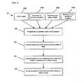
- FIG. 3shows a flow diagram of an illustrative method of yield gradient computation according to the invention.
- FIG. 4shows a flow diagram of an illustrative method of circuit parametric yield optimization by using yield gradients computed according to the invention in conjunction with a nonlinear optimization package.
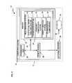
- FIG. 5shows a block diagram of an illustrative system according to the invention.
- the inventionprovides a method, system, and program product for continuously optimizing an integrated circuit based on yield considerations.
- FIGS. 1 A-Baspects of criticality probability analysis, upon which the invention is based, are shown.
- a timing graph 100is shown, comprising a plurality of nodes 110 , 120 , 122 . . . and edges (represented as unidirectional arrows) between pairs of nodes.
- the first or “upstream” node 110is designated the “source” of the timing graph and the terminal node 150 is designated the “sink” of the timing graph.
- the timing graph 100 of FIG. 1Ais provided for purposes of explanation only. An actual timing graph may contain many more nodes and edges than those shown in FIG. 1A .
- Criticality probability analysissuch as that described in U.S. Patent Application Publication No. 20050066298 to Visweswariah, permits calculation of such a probability in an efficient manner.
- the first step in computing the criticality probability of edge Ais to find an appropriate cutset that includes edge A, as shown in FIG. 1A .
- the cutsetdivides the timing graph 100 into two sub-graphs, one of which includes the source node 110 and the other of which includes the sink node 150 . All paths of timing graph 100 must pass through one and precisely one edge of the cutset.
- AT ais the statistical maximum delay from the source node 110 to point a (i.e., node 122 )
- dabis the statistical delay attributable to passage of the signal between points a and b (i.e., along edge A)
- ATs and RATs of nodes of a timing graphare computed by statistical timing analysis as arrival times (AT) and required arrival times (RAT), respectively.
- the edge slack of edge Ais the statistical maximum of the delays of all paths passing through edge A.
- an edge slackis calculated for each edge of the timing graph 100 ( FIG. 1A ) for which its corresponding nodes lie on opposite sides of a cutset (e.g., vertical dotted line of FIG. 1A ).
- a cutsete.g., vertical dotted line of FIG. 1A
- an edge slackwould also typically be calculated for edges B and C.
- a complement edge slackis simply the statistical maximum of the edge slack of all edges in the cutset other than the edge of interest.
- the complement edge slack in the example shown in FIG. 1Ais the statistical maximum of the edge slacks of edges B and C.
- the complement edge slackis the statistical maximum of the delays of all paths not passing through the edge of interest.
- edge Athe edge of interest
- the ensemble longest path through iti.e., its edge slack
- the probability that the edge slack of edge A is statistically larger than the complementary edge slackis the criticality probability of edge A.
- Arrow 170represents the ensemble of all paths of the timing graph 100 ( FIG. 1A ) that do not pass through edge A.
- Arrow 172represents the ensemble of all paths of the timing graph 100 passing through edge A.
- edge slack B of edge Adoes not depend on the delay of edge A, since it represents statistical maximum of delays of the ensemble of paths that do not pass through edge A.
- AT a and RAT bdo not depend on the delay of edge A, since they represent the statistical maximum of delays of the paths “upstream” and “downstream” of edge A, respectively.
- the statistical circuit delay equation abovecan be differentiated to obtain the gradient of the statistical circuit delay to the components of edge A.
- the second stepis to express the parametric yield of the circuit in terms of the statistical circuit delay.
- Yield at a required performanceis simply the probability that the statistical circuit delay is less than the clock cycle time dictated by the performance requirement. Since the optimization of a circuit can be carried out in many different ways, we introduce the concept of a “profit” function whose gradients we seek to compute. Profit is the quantity being maximized or constrained in the optimization.
- a profit functionis the yield at a required performance. This profit function implies that any chip with performance not lower than the requirement can be sold at a constant non-zero profit and any chip with performance lower than the requirement cannot be sold at all.
- Another exampleis the performance at a given required yield.
- Yet another exampleis a weighted sum of the parametric yield in various “bins” or performance ranges. The gradient of any such profit function can be computed once the gradients of the statistical circuit delay are known.
- ⁇ ⁇ 1 ( )denotes the inverse CDF (Cumulative Distribution Function) of a standard normal or Gaussian distribution
- z 0is the mean of z
- ⁇ zis the standard deviation of z.
- the yield gradients obtained abovemay be used in any number of ways useful in optimizing an integrated circuit.
- the circuitmay be optimized to maximize performance at a given yield (e.g., 90%).
- the circuitmay be optimized to maximize yield at a required performance (e.g., clock frequency).
- the circuitmay be optimized to maximize a profit function which is a weighted sum of the parametric yield in each of several “bins” or performance ranges.
- FIG. 3shows an inventive process for computing yield gradients.
- Step S 1shows the usual inputs to statistical timing.
- the first inputis the netlist of the circuit to be analyzed 202 .
- the next inputis the set of timing assertions or timing constraints 204 , which can include primary input arrival times, primary output required arrival times, external loading on the primary outputs, etc.
- a set of parameterized delay models 206 that capture the delay variability of circuit componentsis the third input.
- statistics of the sources of variation 208include process and environmental parameters, comprise the final input. These can include means, standard deviations, distributions, and correlations among the sources of variation.
- step S 2a probabilistic or statistical static timing analysis is carried out using methods known in the art.
- step S 3the statistical circuit delay is expressed in terms of the delay of an edge of interest. This is accomplished by identifying a suitable cutset, computing the edge slack and complement edge slack of the edge of interest, and expressing the statistical circuit delay as a statistical maximum of the edge slack and complement edge slack.
- step S 4the gradient of the mean and standard deviation of the statistical circuit delay with respect to the delay components of the edge of interest are computed by applying the formulas of Appendix A.
- the delay componentsmay in turn be functions of physical parameters such as channel length or metal thickness, and this step includes any chain-ruling of gradients necessary.
- Step S 5the gradients of the profit function are computed by expressing these gradients in terms of the gradients of the mean and standard deviation of the statistical circuit delay.
- Yield gradientscan be used for both discrete and continuous optimization of circuits.
- FIG. 4shows how continuous optimization can be carried out using the inventive yield gradients.
- a problemis formulated, comprising a statement of what is to be minimized or maximized, subject to what constraints, and subject to what simple bounds on the optimization variables.
- the problem statement of step S 101is fed to a nonlinear optimization package at step S 102 .
- the nonlinear optimizercomes up with new assignments to the optimization variables at step S 103 . If convergence has been obtained (“Yes” at step S 104 ), the optimization process is stopped (step S 105 ). Convergence is obtained when the optimization variables cease to change or all optimization goals are met.
- the new optimization variablesare applied to the inventive statistical timer at step 106 .
- the timerproduces both timing results (step S 108 ) as well as yield and/or profit gradients (step S 107 ). These are fed back to the nonlinear optimization package at step S 109 , where the nonlinear optimization package uses all the function and gradient values of the present and all past iterations to come up with the next set of optimization variables. This procedure is carried out until convergence is obtained (“Yes” at step S 104 ) and the optimization process is stopped at step S 105 .
- FIG. 5shows an illustrative system 10 for computing yield gradients from statistical timing.
- system 10includes a computer infrastructure 12 that can perform the various process steps described herein for computing yield gradients from statistical timing.
- computer infrastructure 12is shown including a computer system 14 that comprises a yield gradient system 40 , which enables computer system 14 to compute yield gradients from statistical timing by performing the process steps of the invention.
- Computer system 14is shown including a processing unit 20 , a memory 22 , an input/output (I/O) interface 26 , and a bus 24 . Further, computer system 14 is shown in communication with external devices 28 and a storage system 30 . As is known in the art, in general, processing unit 20 executes computer program code, such as yield gradient system 40 , that is stored in memory 22 and/or storage system 30 . While executing computer program code, processing unit 20 can read and/or write data from/to memory 22 , storage system 30 , and/or I/O interface 26 . Bus 24 provides a communication link between each of the components in computer system 14 . External devices 28 can comprise any device that enables a user (not shown) to interact with computer system 14 or any device that enables computer system 14 to communicate with one or more other computer systems.
- external devices 28can comprise any device that enables a user (not shown) to interact with computer system 14 or any device that enables computer system 14 to communicate with one or more other computer systems.
- computer system 14can comprise any general purpose computing article of manufacture capable of executing computer program code installed by a user (e.g., a personal computer, server, handheld device, etc.).
- computer system 14 and yield gradient system 40are only representative of various possible computer systems that may perform the various process steps of the invention.
- computer system 14can comprise any specific purpose computing article of manufacture comprising hardware and/or computer program code for performing specific functions, any computing article of manufacture that comprises a combination of specific purpose and general purpose hardware/software, or the like.
- the program code and hardwarecan be created using standard programming and engineering techniques, respectively.
- computer infrastructure 12is only illustrative of various types of computer infrastructures for implementing the invention.
- computer infrastructure 12comprises two or more computer systems (e.g., a server cluster) that communicate over any type of wired and/or wireless communications link, such as a network, a shared memory, or the like, to perform the various process steps of the invention.
- the communications linkcomprises a network
- the networkcan comprise any combination of one or more types of networks (e.g., the Internet, a wide area network, a local area network, a virtual private network, etc.).
- communications between the computer systemsmay utilize any combination of various types of transmission techniques.
- yield gradient system 40enables computer system 14 to compute yield gradients from statistical timing.
- yield gradient system 40is shown including a statistical timing analysis system 42 , an expression system 44 , a gradient computation system 46 , and a profit function system 48 . Operation of each of these systems is discussed above.
- Yield gradient system 40may further include other system components 50 to provide additional or improved functionality to yield gradient system 40 . It is understood that some of the various systems shown in FIG. 5 can be implemented independently, combined, and/or stored in memory for one or more separate computer systems 14 that communicate over a network. Further, it is understood that some of the systems and/or functionality may not be implemented, or additional systems and/or functionality may be included as part of system 10 .
- the inventionprovides a computer-readable medium that includes computer program code to enable a computer infrastructure to compute yield gradients from statistical timing.
- the computer-readable mediumincludes program code, such as yield gradient system 40 , that implements each of the various process steps of the invention.
- the term “computer-readable medium”comprises one or more of any type of physical embodiment of the program code.
- the computer-readable mediumcan comprise program code embodied on one or more portable storage articles of manufacture (e.g., a compact disc, a magnetic disk, a tape, etc.), on one or more data storage portions of a computer system, such as memory 22 and/or storage system 30 (e.g., a fixed disk, a read-only memory, a random access memory, a cache memory, etc.), and/or as a data signal traveling over a network (e.g., during a wired/wireless electronic distribution of the program code).
- portable storage articles of manufacturee.g., a compact disc, a magnetic disk, a tape, etc.
- data storage portions of a computer systemsuch as memory 22 and/or storage system 30 (e.g., a fixed disk, a read-only memory, a random access memory, a cache memory, etc.), and/or as a data signal traveling over a network (e.g., during a wired/wireless electronic distribution of the program code).
- storage system 30
- the inventionprovides a business method that performs the process steps of the invention on a subscription, advertising, and/or fee basis. That is, a service provider could offer to compute yield gradients from statistical timing as described above.
- the service providercan create, maintain, support, etc., a computer infrastructure, such as computer infrastructure 12 , that performs the process steps of the invention for one or more customers.
- the service providercan receive payment from the customer(s) under a subscription and/or fee agreement and/or the service provider can receive payment from the sale of advertising space to one or more third parties.
- the inventionprovides a method of generating a system for computing yield gradients from statistical timing.
- a computer infrastructuresuch as computer infrastructure 12
- one or more systems for performing the process steps of the inventioncan be obtained (e.g., created, purchased, used, modified, etc.) and deployed to the computer infrastructure.
- the deployment of each systemcan comprise one or more of (1) installing program code on a computer system, such as computer system 14 , from a computer-readable medium; (2) adding one or more computer systems to the computer infrastructure; and (3) incorporating and/or modifying one or more existing systems of the computer infrastructure, to enable the computer infrastructure to perform the process steps of the invention.
- program codeand “computer program code” are synonymous and mean any expression, in any language, code or notation, of a set of instructions intended to cause a computer system having an information processing capability to perform a particular function either directly or after either or both of the following: (a) conversion to another language, code or notation; and (b) reproduction in a different material form.
- program codecan be embodied as one or more types of program products, such as an application/software program, component software/a library of functions, an operating system, a basic I/O system/driver for a particular computing and/or I/O device, and the like.
- Zmax(A, B).
- ⁇ and ⁇to represent ⁇ ( a 0 - b 0 ⁇ ) ⁇ ⁇ and ⁇ ⁇ ⁇ ( a 0 - b 0 ⁇ ) .
- ⁇ Z 2( ⁇ A 2 + a 0 2 ) ⁇ ⁇ + ( ⁇ B 2 + b 0 2 ) ⁇ ( 1 - ⁇ ) + ( a 0 + b 0 ) ⁇ ⁇ ⁇ ⁇ ⁇ - z 0 2 . ( A ⁇ .12 )
- ⁇ ⁇ Z ⁇ a r⁇ 1 ⁇ Z [ a r ⁇ ⁇ ⁇ ⁇ - ⁇ z 0 ⁇ ⁇ a r ⁇ ⁇ ⁇ ⁇ + ⁇ ⁇ a ⁇ r ⁇ ⁇ a ⁇ 0 + b ⁇ 0 + ⁇ ( a ⁇ 0 ⁇ - ⁇ b ⁇ 0 ) ⁇ ⁇ ⁇ ⁇ B ⁇ 2 ⁇ - ⁇ ⁇ ⁇ A ⁇ 2 ⁇ ⁇ ⁇ 2 ⁇ ⁇ ⁇ 2 ⁇ ⁇ ⁇ ⁇ 2 ⁇ ⁇ ⁇ ] .
Landscapes
- Engineering & Computer Science (AREA)
- Physics & Mathematics (AREA)
- Computer Hardware Design (AREA)
- Theoretical Computer Science (AREA)
- General Physics & Mathematics (AREA)
- Geometry (AREA)
- Evolutionary Computation (AREA)
- General Engineering & Computer Science (AREA)
- Computer Networks & Wireless Communication (AREA)
- Computational Mathematics (AREA)
- Mathematical Analysis (AREA)
- Mathematical Optimization (AREA)
- Pure & Applied Mathematics (AREA)
- Design And Manufacture Of Integrated Circuits (AREA)
Abstract
Description
- 1. Technical Field
- The invention relates generally to computer-aided design of integrated circuits, and more particularly, to the optimization of a digital circuit based on yield considerations. Even more particularly, the invention relates to the computation of yield gradients using statistical timing.
- 2. Background Art
- Variability in integrated circuits increases with each new technology generation. Sources of variability include manufacturing conditions, device fatigue, environmental variations, and phase-locked loop (PLL) variations.
- In the past, static timing analyses have been used to determine the performance of a circuit. In static timing analysis, a circuit is mapped to a graph called a timing graph. The longest path through the timing graph is the performance-limiting (i.e., critical) path of the circuit. If the delay of the critical path is more than a required value, the circuit cannot function properly. That is, the circuit has a timing violation. Because of variability, only a fraction of all manufactured circuits can meet the required timing constraints. This fraction is called the parametric yield of the circuit.
- Typically, a static timing analysis is conducted for a particular setting of each of the process and environmental parameters, such as the thickness of a metal layer, the lengths of transistors, temperature, supply voltage, etc. The set of values to which process parameters are assigned is called a process corner. Such a static timing analysis at a particular process corner is referred to as “deterministic” timing analysis.
- Deterministic timing analysis only verifies timing at a few selected process corners. Because of variability, multiple deterministic timing analyses are generally required to accurately analyze a circuit. When a large number of independently variable process parameters must be modeled, the number of timing runs necessary using traditional deterministic static timing analysis makes such a method impractical. Optimization of circuits based on deterministic timing analysis is also problematic. In the presence of process variations, the critical path is no longer unique. In fact, each process corner may have a different critical path. Thus, guiding optimization by the results of a deterministic timing analysis may not be the most efficient way to optimize a circuit.
- These problems are partially overcome by statistical or probabilistic timing analysis, as taught in Patent Application Publication No. 20050065765 to Visweswariah, which is hereby incorporated by reference. In such an analysis, timing quantities such as delays, arrival times, and slacks are not treated as single numbers, but as correlated probability distributions. As such, the full probability distribution of the performance of the circuit under the influence of variations is predicted by a single timing run.
- In such a run, the statistical maximum of the delay of all paths of the circuit is predicted. This quantity is called “statistical circuit delay.” It is to be noted that this quantity is not the delay of any particular path. Rather, it represents the statistical maximum of the delay of all paths of the circuit.
- In addition to timing analysis, an important role of a static timing analyzer is to provide diagnostics that are useful for optimization of the circuit. Such optimization may be automated or manual, and discrete or continuous. Since the critical path is not unique, as explained above, diagnostics that cover the entire space of process variations are especially important. The concept of criticality was taught in Patent Application Publication No. 20050066298 to Visweswariah, which is hereby incorporated by reference. Simply defined, the criticality probability of an edge, node, or path of a timing graph is the probability of manufacturing a chip in which the edge, node or path is in the critical path. An efficient method of computing criticality probabilities of all edges of a timing graph was also taught in U.S. Patent Application Publication No. 20050066298.
- Recently, a method for computing the sensitivity of the mean of the circuit's longest path to the mean or nominal delay of each circuit component was taught in “Defining statistical sensitivity for timing optimization of logic circuits with large-scale process and environmental variations” by Xin Li et al the IEEE International Conference on Computer-Aided Design, San Jose, Calif., November 2005. Unfortunately, this method does not compute yield gradients, and the sensitivities are computed by an inefficient chain-ruling method that propagates sensitivities through the timing graph.
- Recently, a method for computing sensitivities in the context of statistical timing was taught by K. Chopra et al., “Parametric yield maximization using gate sizing based on efficient statistical power and delay gradient computation,” at the International Conference on Computer-Aided Design, San Jose, Calif., November 2005. While this approach uses the concept of a cutset, it uses a numerical perturbation method for sensitivity computation, which is neither efficient nor accurate.
- While criticality computation and sensitivity analysis provide valuable diagnostics, they still do not provide sufficient data for fully optimizing a circuit. More efficient optimization may be achieved if one were to know the gradient of a parametric yield (i.e., the circuit's yield due to variation in process parameters) with respect to the delay characteristics of one or more circuit components, e.g., the delay of each gate or the size of each transistor. To this extent, a need exists for a method for determining the gradient of a parametric yield relative to the delay characteristics or designable parameters of a circuit component.
- The invention provides a method, system, and program product for determining a gradient of a yield of an integrated circuit with respect to parameters (characteristics) of a delay of an edge of a timing graph of the circuit.
- A first aspect of the invention provides a method for determining a gradient of a parametric yield of an integrated circuit with respect to parameters of a delay of an edge of a timing graph of the circuit, the method comprising: conducting a statistical timing analysis; expressing a statistical circuit delay in terms of a delay of the edge; and computing a gradient of the statistical circuit delay with respect to parameters of the delay of the edge.
- A second aspect of the invention provides a system for determining a gradient of a parametric yield of an integrated circuit with respect to parameters of a delay of an edge of a timing graph of the circuit, the system comprising: a system for conducting a statistical timing analysis; a system for expressing a statistical circuit delay in terms of a delay of the edge; and a system for computing a gradient of the statistical circuit delay with respect to parameters of the delay of the edge.
- A third aspect of the invention provides a program product stored on a computer-readable medium, which when executed, determines a gradient of a parametric yield of an integrated circuit with respect to parameters of a delay of an edge of a timing graph of the circuit, the program product comprising: program code for conducting a statistical timing analysis; program code for expressing statistical circuit delay in terms of a delay of the edge; and program code for computing a gradient of the statistical circuit delay with respect to parameters of the delay of the edge.
- A fourth aspect of the invention provides a method for deploying an application for determining a gradient of a parametric yield of an integrated circuit with respect to parameters of a delay of an edge of a timing graph of the circuit, comprising: providing a computer infrastructure being operable to: conduct a statistical timing analysis; express statistical circuit delay in terms of a delay of the edge; and compute a gradient of the statistical circuit delay with respect to parameters of the delay of the edge.
- A fifth aspect of the invention provides a business method for determining a gradient of a parametric yield of an integrated circuit with respect to parameters of a delay of an edge of a timing graph of the circuit.
- The illustrative aspects of the present invention are designed to solve the problems herein described and other problems not discussed, which are discoverable by a skilled artisan.
- These and other features of this invention will be more readily understood from the following detailed description of the various aspects of the invention taken in conjunction with the accompanying drawings that depict various embodiments of the invention, in which:
- FIGS.1A-B show aspects of a criticality probability analysis.
FIG. 2 shows a graphical representation of a step in the computation of a yield gradient according to the invention.FIG. 3 shows a flow diagram of an illustrative method of yield gradient computation according to the invention.FIG. 4 shows a flow diagram of an illustrative method of circuit parametric yield optimization by using yield gradients computed according to the invention in conjunction with a nonlinear optimization package.FIG. 5 shows a block diagram of an illustrative system according to the invention.- It is noted that the drawings of the invention are not to scale. The drawings are intended to depict only typical aspects of the invention, and therefore should not be considered as limiting the scope of the invention. In the drawings, like numbering represents like elements between the drawings.
- As indicated above, the invention provides a method, system, and program product for continuously optimizing an integrated circuit based on yield considerations.
- Referring now to FIGS.1A-B, aspects of criticality probability analysis, upon which the invention is based, are shown. In
FIG. 1A , atiming graph 100 is shown, comprising a plurality ofnodes node 110 is designated the “source” of the timing graph and theterminal node 150 is designated the “sink” of the timing graph. Thetiming graph 100 ofFIG. 1A is provided for purposes of explanation only. An actual timing graph may contain many more nodes and edges than those shown inFIG. 1A . - In performing a criticality probability analysis, one determines the probability of manufacturing an integrated circuit (i.e., a chip) in which a particular edge or node is included in the critical path. For example, in
FIG. 1A , one may wish to know the probability that edge A (shown as a broken arrow betweennodes 122 and132) will lie in the critical path of the chip. Criticality probability analysis, such as that described in U.S. Patent Application Publication No. 20050066298 to Visweswariah, permits calculation of such a probability in an efficient manner. - The first step in computing the criticality probability of edge A is to find an appropriate cutset that includes edge A, as shown in
FIG. 1A . The cutset divides thetiming graph 100 into two sub-graphs, one of which includes thesource node 110 and the other of which includes thesink node 150. All paths oftiming graph 100 must pass through one and precisely one edge of the cutset. - In
FIG. 1B ,timing graph 100 ofFIG. 1A has been simplified to show only those paths including edge A. Upstream nodes andedges 160 and downstream nodes andedges 162 are shown in simplified form. FromFIG. 1B , an edge slack can be computed using the following equation:
Edge slack=ATa+dab−RATb,
wherein ATais the statistical maximum delay from thesource node 110 to point a (i.e., node122), dab is the statistical delay attributable to passage of the signal between points a and b (i.e., along edge A), and RATbis the negative of the statistical maximum delay from point b (i.e., node132) to thesink node 150. ATs and RATs of nodes of a timing graph are computed by statistical timing analysis as arrival times (AT) and required arrival times (RAT), respectively. The edge slack of edge A is the statistical maximum of the delays of all paths passing through edge A. Typically, an edge slack is calculated for each edge of the timing graph100 (FIG. 1A ) for which its corresponding nodes lie on opposite sides of a cutset (e.g., vertical dotted line ofFIG. 1A ). For example, referring toFIG. 1A , an edge slack would also typically be calculated for edges B and C. - According to the invention, additional computational steps are performed in addition to those shown above. First, a complement edge slack is computed. A complement edge slack is simply the statistical maximum of the edge slack of all edges in the cutset other than the edge of interest. The complement edge slack in the example shown in
FIG. 1A is the statistical maximum of the edge slacks of edges B and C. The complement edge slack is the statistical maximum of the delays of all paths not passing through the edge of interest. Next, one computes the probability that the edge slack of edge A is statistically larger than the complement edge slack. This probability is the criticality probability of edge A. - The purpose of these additional steps is to find the total probability of the criticality of all paths that pass through the edge of interest (i.e., edge A). Since every path of the timing graph100 (
FIG. 1A ) goes through precisely one edge of the cutset, for the edge to be included in the critical path, the ensemble longest path through it (i.e., its edge slack) must be larger than all other edge slacks. Thus, the probability that the edge slack of edge A is statistically larger than the complementary edge slack is the criticality probability of edge A. - U.S. Patent Application Publication No. 20050066298 to Visweswariah teaches efficient ways of finding suitable cutsets, efficient ways of computing edge slacks, efficient ways of processing the edge slacks of a cutset to obtain complement edge slacks, and efficient ways of computing the criticality probabilities of all edges of a timing graph.
- The above computations do not, by themselves, provide a measure of how the parametric yield of the circuit is impacted by changing the delay characteristics of an edge of the timing graph. This problem is overcome by the present invention, particularly the steps described below, which provide the gradient of the parametric yield of a chip to all components of the statistical delay model of an edge of the timing graph. Computation of the yield gradient requires two additional steps. First, the dependence of the statistical circuit delay on the delay of a single edge must be isolated. Second, the parametric yield of the circuit must be expressed in terms of the cumulative distribution function (CDF) of the statistical delay of the circuit. The requisite yield gradients can then be obtained from the above two steps.
- Referring now to
FIG. 2 , a figure useful in describing the derivation of yield gradients is shown.Arrow 170 represents the ensemble of all paths of the timing graph100 (FIG. 1A ) that do not pass through edge A. The statistical maximum of all delays of these paths is the complement edge slack of edge A. It can be expressed by the equation
wherein Xirepresents globally correlated random variation, i=1, 2, . . . , n, XBrepresents uncorrelated random variation, b0represents the mean or nominal delay, birepresents the sensitivity to random variation Xi, and brrepresents the sensitivity to random variation XB. - The above equation assumes that all statistical quantities are expressed in a so-called “first-order canonical form” taught in Patent Application Publication No. 200500665298 to Visweswariah. It is to be noted that the present invention can be applied to any other form that is chosen for expressing statistical quantities.
Arrow 172, on the other hand, represents the ensemble of all paths of thetiming graph 100 passing through edge A. The arrival time (AT) atnode 122 represents the statistical maximum of the delay of the ensemble of paths from thesource node 110 tonode 122 and may be represented by the equation:
wherein Xirepresents globally correlated random variation, i=1, 2, . . . , n, XATrepresents uncorrelated random variation, AT0represents the mean or nominal arrival time, ATirepresents the sensitivity to random variation Xi, and ATrrepresents the sensitivity to random variation XAT.- Similarly, the required arrival time (RAT) at
node 132 represents the negative of the statistical maximum of the delay of the ensemble of paths fromnode 132 to thesink node 150 and may be represented by the equation:
wherein Xirepresents globally correlated random variation, i=1, 2, . . . , n, XRATrepresents uncorrelated random variation, RAT0represents the mean or nominal required arrival time, RATirepresents the sensitivity to random variation Xi, and RATrrepresents the sensitivity to random variation XRAT. - Finally, the delay attributable to edge A itself may be represented by the equation:
wherein Xirepresents globally correlated random variation, i=1, 2, . . . , n, XDelayrepresents uncorrelated random variation, Delay0represents the mean or nominal delay, Delayirepresents the sensitivity to random variation Xi,and Delayrrepresents the sensitivity to random variation XDelay. - As can be seen in
FIG. 2 , all paths of the timing graph100 (FIG. 1A ) have been separated into two groups: those that pass through edge A and those that do not. This effectively isolates the impact of edge A on the statistical circuit delay. - Next, the statistical circuit delay is expressed as the statistical maximum of the delay of all circuit paths in
FIG. 2 : - It should be noted that the complement edge slack B of edge A does not depend on the delay of edge A, since it represents statistical maximum of delays of the ensemble of paths that do not pass through edge A. Similarly, ATaand RATbdo not depend on the delay of edge A, since they represent the statistical maximum of delays of the paths “upstream” and “downstream” of edge A, respectively. As a result, the statistical circuit delay equation above can be differentiated to obtain the gradient of the statistical circuit delay to the components of edge A.
- The statistical maximum operation in the equation above can be approximated analytically according to Clark, C. E., “The greatest of a finite set of random variables,” Operations Research, 145-162 (1961). The equations thereof may be differentiated in a straightforward manner to obtain the gradients of the following functions:
- Mean of the longest path delay; and
- Standard deviation of the longest path delay,
with respect to the following parameters: - Mean of the delay of any edge of interest (edge A in the example of
FIG. 1A ); - Sensitivity of the delay of any edge of interest (edge A in the example of
FIG. 1A ) to any globally correlated random variation (Delayiin this example); and - Sensitivity of the delay of any edge of interest (edge A in the example of
FIG. 1A ) to uncorrelated random variation (Delayrin this example).
Equations to perform such a straightforward differentiation of the statistical maximum operation are shown in Appendix A. - The second step is to express the parametric yield of the circuit in terms of the statistical circuit delay. Yield at a required performance is simply the probability that the statistical circuit delay is less than the clock cycle time dictated by the performance requirement. Since the optimization of a circuit can be carried out in many different ways, we introduce the concept of a “profit” function whose gradients we seek to compute. Profit is the quantity being maximized or constrained in the optimization. One example of a profit function is the yield at a required performance. This profit function implies that any chip with performance not lower than the requirement can be sold at a constant non-zero profit and any chip with performance lower than the requirement cannot be sold at all. Another example is the performance at a given required yield. Yet another example is a weighted sum of the parametric yield in various “bins” or performance ranges. The gradient of any such profit function can be computed once the gradients of the statistical circuit delay are known.
- Let us first consider a profit function, which is the performance at a given yield, p, a constant. Let the statistical circuit delay be z. The statistical circuit delay that meets the yield requirement p is denoted by z(p), which can be written as
z(p)=Φ−1(p)σz+z0,
where Φ−1( ) denotes the inverse CDF (Cumulative Distribution Function) of a standard normal or Gaussian distribution, z0is the mean of z, and σzis the standard deviation of z. Thus the gradient with respect to some delay component of some edge diis
which in turn is easily computed since gradients of the mean and standard deviation of z are known by applying the formulas in Appendix A. - Next, we consider a profit function which is the yield at a given performance, which translates into a requirement that the statistical circuit delay be less than or equal to T. The yield is therefore
which can be differentiated to obtain the necessary profit gradients
where φ( ) represents the PDF (Probability Density Function) of a standard normal or Gaussian distribution. - It is to be understood that once the gradients of the statistical circuit delay are known, one of ordinary skill in the art can derive methods for computing the gradients of various profit functions.
- The yield gradients obtained above may be used in any number of ways useful in optimizing an integrated circuit. For example, the circuit may be optimized to maximize performance at a given yield (e.g., 90%). Alternatively, the circuit may be optimized to maximize yield at a required performance (e.g., clock frequency). Or the circuit may be optimized to maximize a profit function which is a weighted sum of the parametric yield in each of several “bins” or performance ranges.
- In accordance with the above,
FIG. 3 shows an inventive process for computing yield gradients. Step S1 shows the usual inputs to statistical timing. The first input is the netlist of the circuit to be analyzed202. The next input is the set of timing assertions or timingconstraints 204, which can include primary input arrival times, primary output required arrival times, external loading on the primary outputs, etc. A set of parameterizeddelay models 206 that capture the delay variability of circuit components is the third input. Finally, statistics of the sources ofvariation 208, including process and environmental parameters, comprise the final input. These can include means, standard deviations, distributions, and correlations among the sources of variation. - In step S2, a probabilistic or statistical static timing analysis is carried out using methods known in the art. In step S3, the statistical circuit delay is expressed in terms of the delay of an edge of interest. This is accomplished by identifying a suitable cutset, computing the edge slack and complement edge slack of the edge of interest, and expressing the statistical circuit delay as a statistical maximum of the edge slack and complement edge slack.
- In step S4, the gradient of the mean and standard deviation of the statistical circuit delay with respect to the delay components of the edge of interest are computed by applying the formulas of Appendix A. The delay components may in turn be functions of physical parameters such as channel length or metal thickness, and this step includes any chain-ruling of gradients necessary.
- Finally, in Step S5, the gradients of the profit function are computed by expressing these gradients in terms of the gradients of the mean and standard deviation of the statistical circuit delay.
- Yield gradients can be used for both discrete and continuous optimization of circuits.
FIG. 4 shows how continuous optimization can be carried out using the inventive yield gradients. At step S101 a problem is formulated, comprising a statement of what is to be minimized or maximized, subject to what constraints, and subject to what simple bounds on the optimization variables. The problem statement of step S101 is fed to a nonlinear optimization package at step S102. At each iteration of the optimization, the nonlinear optimizer comes up with new assignments to the optimization variables at step S103. If convergence has been obtained (“Yes” at step S104), the optimization process is stopped (step S105). Convergence is obtained when the optimization variables cease to change or all optimization goals are met. Otherwise (“No” at step S104), the new optimization variables are applied to the inventive statistical timer atstep 106. The timer produces both timing results (step S108) as well as yield and/or profit gradients (step S107). These are fed back to the nonlinear optimization package at step S109, where the nonlinear optimization package uses all the function and gradient values of the present and all past iterations to come up with the next set of optimization variables. This procedure is carried out until convergence is obtained (“Yes” at step S104) and the optimization process is stopped at step S105. - Although the above detailed description was explained in terms of late-mode timing, it is to be understood that one of ordinary skill in the art can apply the same concepts to early-mode timing. Similarly, the assumptions of Gaussian distributions or first-order canonical statistical quantities were made for demonstration purposes only, and the concepts apply to any distributions and any form chosen for statistical quantities. Although the above gradient computation was explained for one edge of interest, gradient computation for some or all edge delays can be computed simultaneously by the inventive method. While gradient computation with respect to delay components was explained, gradient computation with respect to dimensions (transistor width, length, wire length) or environmental values (temperature, supply voltage) or component values (resistance values, capacitance values) can be computed by the inventive method by chain-ruling that will be known to one skilled in the art. The inventive techniques are applicable to all kinds of circuits, including combinational and sequential, and gate-level, block-level transistor-level, or mixed-level circuit representations.
FIG. 5 shows anillustrative system 10 for computing yield gradients from statistical timing. To this extent,system 10 includes acomputer infrastructure 12 that can perform the various process steps described herein for computing yield gradients from statistical timing. In particular,computer infrastructure 12 is shown including acomputer system 14 that comprises ayield gradient system 40, which enablescomputer system 14 to compute yield gradients from statistical timing by performing the process steps of the invention.Computer system 14 is shown including aprocessing unit 20, amemory 22, an input/output (I/O)interface 26, and abus 24. Further,computer system 14 is shown in communication withexternal devices 28 and astorage system 30. As is known in the art, in general, processingunit 20 executes computer program code, such asyield gradient system 40, that is stored inmemory 22 and/orstorage system 30. While executing computer program code, processingunit 20 can read and/or write data from/tomemory 22,storage system 30, and/or I/O interface 26.Bus 24 provides a communication link between each of the components incomputer system 14.External devices 28 can comprise any device that enables a user (not shown) to interact withcomputer system 14 or any device that enablescomputer system 14 to communicate with one or more other computer systems.- In any event,
computer system 14 can comprise any general purpose computing article of manufacture capable of executing computer program code installed by a user (e.g., a personal computer, server, handheld device, etc.). However, it is understood thatcomputer system 14 andyield gradient system 40 are only representative of various possible computer systems that may perform the various process steps of the invention. To this extent, in other embodiments,computer system 14 can comprise any specific purpose computing article of manufacture comprising hardware and/or computer program code for performing specific functions, any computing article of manufacture that comprises a combination of specific purpose and general purpose hardware/software, or the like. In each case, the program code and hardware can be created using standard programming and engineering techniques, respectively. - Similarly,
computer infrastructure 12 is only illustrative of various types of computer infrastructures for implementing the invention. For example, in one embodiment,computer infrastructure 12 comprises two or more computer systems (e.g., a server cluster) that communicate over any type of wired and/or wireless communications link, such as a network, a shared memory, or the like, to perform the various process steps of the invention. When the communications link comprises a network, the network can comprise any combination of one or more types of networks (e.g., the Internet, a wide area network, a local area network, a virtual private network, etc.). Regardless, communications between the computer systems may utilize any combination of various types of transmission techniques. - As previously mentioned,
yield gradient system 40 enablescomputer system 14 to compute yield gradients from statistical timing. To this extent,yield gradient system 40 is shown including a statisticaltiming analysis system 42, anexpression system 44, agradient computation system 46, and aprofit function system 48. Operation of each of these systems is discussed above.Yield gradient system 40 may further includeother system components 50 to provide additional or improved functionality to yieldgradient system 40. It is understood that some of the various systems shown inFIG. 5 can be implemented independently, combined, and/or stored in memory for one or moreseparate computer systems 14 that communicate over a network. Further, it is understood that some of the systems and/or functionality may not be implemented, or additional systems and/or functionality may be included as part ofsystem 10. - While shown and described herein as a method and system for computing yield gradients from statistical timing, it is understood that the invention further provides various alternative embodiments. For example, in one embodiment, the invention provides a computer-readable medium that includes computer program code to enable a computer infrastructure to compute yield gradients from statistical timing. To this extent, the computer-readable medium includes program code, such as
yield gradient system 40, that implements each of the various process steps of the invention. It is understood that the term “computer-readable medium” comprises one or more of any type of physical embodiment of the program code. In particular, the computer-readable medium can comprise program code embodied on one or more portable storage articles of manufacture (e.g., a compact disc, a magnetic disk, a tape, etc.), on one or more data storage portions of a computer system, such asmemory 22 and/or storage system30 (e.g., a fixed disk, a read-only memory, a random access memory, a cache memory, etc.), and/or as a data signal traveling over a network (e.g., during a wired/wireless electronic distribution of the program code). - In another embodiment, the invention provides a business method that performs the process steps of the invention on a subscription, advertising, and/or fee basis. That is, a service provider could offer to compute yield gradients from statistical timing as described above. In this case, the service provider can create, maintain, support, etc., a computer infrastructure, such as
computer infrastructure 12, that performs the process steps of the invention for one or more customers. In return, the service provider can receive payment from the customer(s) under a subscription and/or fee agreement and/or the service provider can receive payment from the sale of advertising space to one or more third parties. - In still another embodiment, the invention provides a method of generating a system for computing yield gradients from statistical timing. In this case, a computer infrastructure, such as
computer infrastructure 12, can be obtained (e.g., created, maintained, having made available to, etc.) and one or more systems for performing the process steps of the invention can be obtained (e.g., created, purchased, used, modified, etc.) and deployed to the computer infrastructure. To this extent, the deployment of each system can comprise one or more of (1) installing program code on a computer system, such ascomputer system 14, from a computer-readable medium; (2) adding one or more computer systems to the computer infrastructure; and (3) incorporating and/or modifying one or more existing systems of the computer infrastructure, to enable the computer infrastructure to perform the process steps of the invention. - As used herein, it is understood that the terms “program code” and “computer program code” are synonymous and mean any expression, in any language, code or notation, of a set of instructions intended to cause a computer system having an information processing capability to perform a particular function either directly or after either or both of the following: (a) conversion to another language, code or notation; and (b) reproduction in a different material form. To this extent, program code can be embodied as one or more types of program products, such as an application/software program, component software/a library of functions, an operating system, a basic I/O system/driver for a particular computing and/or I/O device, and the like.
- The foregoing description of various aspects of the invention has been presented for purposes of illustration and description. It is not intended to be exhaustive or to limit the invention to the precise form disclosed, and obviously, many modifications and variations are possible. Such modifications and variations that may be apparent to a person skilled in the art are intended to be included within the scope of the invention as defined by the accompanying claims.
- Formulas for differentiation of the statistical maximum operation are included in this Appendix.
- Differentiation of the Max Operation
- This Appendix derives formulas for differentiation of the statistical max operator with respect to its arguments. While this appendix assumes that the max operator is implemented as taught in C. Visweswariah et al, “First-order incremental block-based statistical timing analysis,” Proceedings of the 2004 Design Automation Conference, San Diego, Calif., June 2004, it is to be understood that similar differentiation formulas can be readily derived for any other method of implementing the max operator. Likewise, formulas for differentiation of the min operator can also be derived.
- A.1 Preliminaries
- Let A and B be two first-order canonical forms
A=a0+ΣaiXi+arXA, (A.1)
B=b0+ΣbXi+brXB, (A.2)
where Xiare the correlated unit-Gaussian random variations, XAand XBare uncorrelated unit-Gaussian random variations, aiand biare sensitivities to correlated random variations, and arand brare the sensitivities to uncorrelated random variations, respectively. The variance of A and B and their covariance are
σ2A==Σa2i+a2r, (A.3)
σ2B=Σb2i+b2r, (A.4)
cov(A,B)=Σaibi. (A.5) - Some frequently-used equations are listed below.
- Let Z=max(A, B). The mean of Z is given by
- For simplicity, we have used φ and Φ to represent
- This notation will be used wherever there is no ambiguity.
- The variance of Z is
- We are interested in the sensitivity of z0and σZto the ai, bi, arand brparameters. Because of the symmetry between A and B, we will only focus on the derivation of sensitivity with respect to a0, aiand ar.
- A.2 Sensitivity of Mean
- A.2.1 With Respect to Mean
- We first derive the sensitivity of z0with respect to a0.
- It is easy to show that the following equations hold.
- Therefore, we have
A.2.2 With Respect to Correlated Sensitivity - Next, we derive the sensitivity of z0with respect to the correlated sensitivity term ai.
- It is easy to show that the following equations hold.
- Therefore, we have
- We need to compute
which is given by - Therefore, in summary, we have
A.2.3 With Respect to Uncorrelated Sensitivity - We derive the sensitivity of z0with respect to the uncorrelated sensitivity term ar.
- It is easy to show that the following equations hold.
- Therefore, we have
- We need to compute
which is given by - Therefore, in summary, we have
A.3 Sensitivity of Sigma
A.3.1 With Respect to Mean - We derive the sensitivity of σZwith respect to a0.
- Therefore, in summary, we have
A.3.2 With Respect to Correlated Sensitivity - We derive the sensitivity of σZwith respect to the correlated sensitivity term ai.
- Therefore, the sensitivity can be computed as
- Finally,
A.3.3 With Respect to Uncorrelated Sensitivity - We derive the sensitivity of σZwith respect to the uncorrelated term ar.
- Therefore, the sensitivity can be computed as
- Finally,
Claims (24)
Priority Applications (1)
| Application Number | Priority Date | Filing Date | Title |
|---|---|---|---|
| US11/358,622US7480880B2 (en) | 2006-02-21 | 2006-02-21 | Method, system, and program product for computing a yield gradient from statistical timing |
Applications Claiming Priority (1)
| Application Number | Priority Date | Filing Date | Title |
|---|---|---|---|
| US11/358,622US7480880B2 (en) | 2006-02-21 | 2006-02-21 | Method, system, and program product for computing a yield gradient from statistical timing |
Publications (2)
| Publication Number | Publication Date |
|---|---|
| US20070234252A1true US20070234252A1 (en) | 2007-10-04 |
| US7480880B2 US7480880B2 (en) | 2009-01-20 |
Family
ID=38561002
Family Applications (1)
| Application Number | Title | Priority Date | Filing Date |
|---|---|---|---|
| US11/358,622Expired - Fee RelatedUS7480880B2 (en) | 2006-02-21 | 2006-02-21 | Method, system, and program product for computing a yield gradient from statistical timing |
Country Status (1)
| Country | Link |
|---|---|
| US (1) | US7480880B2 (en) |
Cited By (37)
| Publication number | Priority date | Publication date | Assignee | Title |
|---|---|---|---|---|
| US20090100393A1 (en)* | 2007-10-11 | 2009-04-16 | Chandramouli Visweswariah | Method and apparatus for incrementally computing criticality and yield gradient |
| US20100006900A1 (en)* | 2006-03-09 | 2010-01-14 | Tela Innovations, Inc. | Semiconductor Device Portion Having Sub-Wavelength-Sized Gate Electrode Conductive Structures Formed from Rectangular Shaped Gate Electrode Layout Features and Having Equal Number of PMOS and NMOS Transistors |
| US20100023917A1 (en)* | 2003-02-25 | 2010-01-28 | The Regents Of The University Of California | Tool for modifying mask design layout |
| US7730432B1 (en) | 2005-03-30 | 2010-06-01 | Tela Innovations, Inc. | Method and system for reshaping a transistor gate in an integrated circuit to achieve a target objective |
| US20100169847A1 (en)* | 2005-05-06 | 2010-07-01 | Tela Innovations. Inc., A Delaware Corporation | Standard cells having transistors annotated for gate-length biasing |
| US7888705B2 (en) | 2007-08-02 | 2011-02-15 | Tela Innovations, Inc. | Methods for defining dynamic array section with manufacturing assurance halo and apparatus implementing the same |
| US20110041114A1 (en)* | 2009-08-17 | 2011-02-17 | Fujitsu Limited | Circuit design support apparatus, circuit design support method, and circuit design support program |
| US7932545B2 (en) | 2006-03-09 | 2011-04-26 | Tela Innovations, Inc. | Semiconductor device and associated layouts including gate electrode level region having arrangement of six linear conductive segments with side-to-side spacing less than 360 nanometers |
| US7939443B2 (en) | 2008-03-27 | 2011-05-10 | Tela Innovations, Inc. | Methods for multi-wire routing and apparatus implementing same |
| US7943967B2 (en) | 2006-03-09 | 2011-05-17 | Tela Innovations, Inc. | Semiconductor device and associated layouts including diffusion contact placement restriction based on relation to linear conductive segments |
| US7956421B2 (en) | 2008-03-13 | 2011-06-07 | Tela Innovations, Inc. | Cross-coupled transistor layouts in restricted gate level layout architecture |
| US20110140745A1 (en)* | 2009-12-15 | 2011-06-16 | International Business Machines Corporatino | Method for Modeling Variation in a Feedback Loop of a Phase-Locked Loop |
| US7979829B2 (en) | 2007-02-20 | 2011-07-12 | Tela Innovations, Inc. | Integrated circuit cell library with cell-level process compensation technique (PCT) application and associated methods |
| US7994545B2 (en) | 2007-10-26 | 2011-08-09 | Tela Innovations, Inc. | Methods, structures, and designs for self-aligning local interconnects used in integrated circuits |
| US20110231806A1 (en)* | 2010-01-13 | 2011-09-22 | Andreas-Juergen Rohatschek | Method for partitioning electronic units |
| US8127266B1 (en) | 2005-05-06 | 2012-02-28 | Tela Innovations, Inc. | Gate-length biasing for digital circuit optimization |
| US8214778B2 (en) | 2007-08-02 | 2012-07-03 | Tela Innovations, Inc. | Methods for cell phasing and placement in dynamic array architecture and implementation of the same |
| US8225261B2 (en) | 2006-03-09 | 2012-07-17 | Tela Innovations, Inc. | Methods for defining contact grid in dynamic array architecture |
| US8225239B2 (en) | 2006-03-09 | 2012-07-17 | Tela Innovations, Inc. | Methods for defining and utilizing sub-resolution features in linear topology |
| US8245180B2 (en) | 2006-03-09 | 2012-08-14 | Tela Innovations, Inc. | Methods for defining and using co-optimized nanopatterns for integrated circuit design and apparatus implementing same |
| US8247846B2 (en) | 2006-03-09 | 2012-08-21 | Tela Innovations, Inc. | Oversized contacts and vias in semiconductor chip defined by linearly constrained topology |
| US8286107B2 (en) | 2007-02-20 | 2012-10-09 | Tela Innovations, Inc. | Methods and systems for process compensation technique acceleration |
| US8448102B2 (en) | 2006-03-09 | 2013-05-21 | Tela Innovations, Inc. | Optimizing layout of irregular structures in regular layout context |
| US8453094B2 (en) | 2008-01-31 | 2013-05-28 | Tela Innovations, Inc. | Enforcement of semiconductor structure regularity for localized transistors and interconnect |
| US8541879B2 (en) | 2007-12-13 | 2013-09-24 | Tela Innovations, Inc. | Super-self-aligned contacts and method for making the same |
| US8631362B1 (en)* | 2012-10-15 | 2014-01-14 | Berkeley Design Automation, Inc. | Circuit instance variation probability system and method |
| US8653857B2 (en) | 2006-03-09 | 2014-02-18 | Tela Innovations, Inc. | Circuitry and layouts for XOR and XNOR logic |
| US8661392B2 (en) | 2009-10-13 | 2014-02-25 | Tela Innovations, Inc. | Methods for cell boundary encroachment and layouts implementing the Same |
| US8658542B2 (en) | 2006-03-09 | 2014-02-25 | Tela Innovations, Inc. | Coarse grid design methods and structures |
| US8667443B2 (en) | 2007-03-05 | 2014-03-04 | Tela Innovations, Inc. | Integrated circuit cell library for multiple patterning |
| US8839175B2 (en) | 2006-03-09 | 2014-09-16 | Tela Innovations, Inc. | Scalable meta-data objects |
| US8863063B2 (en) | 2009-05-06 | 2014-10-14 | Tela Innovations, Inc. | Finfet transistor circuit |
| US9035359B2 (en) | 2006-03-09 | 2015-05-19 | Tela Innovations, Inc. | Semiconductor chip including region including linear-shaped conductive structures forming gate electrodes and having electrical connection areas arranged relative to inner region between transistors of different types and associated methods |
| US9122832B2 (en) | 2008-08-01 | 2015-09-01 | Tela Innovations, Inc. | Methods for controlling microloading variation in semiconductor wafer layout and fabrication |
| US9159627B2 (en) | 2010-11-12 | 2015-10-13 | Tela Innovations, Inc. | Methods for linewidth modification and apparatus implementing the same |
| US9230910B2 (en) | 2006-03-09 | 2016-01-05 | Tela Innovations, Inc. | Oversized contacts and vias in layout defined by linearly constrained topology |
| US9563733B2 (en) | 2009-05-06 | 2017-02-07 | Tela Innovations, Inc. | Cell circuit and layout with linear finfet structures |
Families Citing this family (1)
| Publication number | Priority date | Publication date | Assignee | Title |
|---|---|---|---|---|
| JP2010160787A (en)* | 2008-12-11 | 2010-07-22 | Jedat Inc | System for creating parameter information, system for estimating yields, program and recording medium |
Citations (2)
| Publication number | Priority date | Publication date | Assignee | Title |
|---|---|---|---|---|
| US5886908A (en)* | 1997-03-27 | 1999-03-23 | International Business Machines Corporation | Method of efficient gradient computation |
| US20070143722A1 (en)* | 2005-12-16 | 2007-06-21 | International Business Machines Corporation | System and method of criticality prediction in statistical timing analysis |
Family Cites Families (2)
| Publication number | Priority date | Publication date | Assignee | Title |
|---|---|---|---|---|
| US7428716B2 (en) | 2003-09-19 | 2008-09-23 | International Business Machines Corporation | System and method for statistical timing analysis of digital circuits |
| US7086023B2 (en) | 2003-09-19 | 2006-08-01 | International Business Machines Corporation | System and method for probabilistic criticality prediction of digital circuits |
- 2006
- 2006-02-21USUS11/358,622patent/US7480880B2/ennot_activeExpired - Fee Related
Patent Citations (2)
| Publication number | Priority date | Publication date | Assignee | Title |
|---|---|---|---|---|
| US5886908A (en)* | 1997-03-27 | 1999-03-23 | International Business Machines Corporation | Method of efficient gradient computation |
| US20070143722A1 (en)* | 2005-12-16 | 2007-06-21 | International Business Machines Corporation | System and method of criticality prediction in statistical timing analysis |
Cited By (212)
| Publication number | Priority date | Publication date | Assignee | Title |
|---|---|---|---|---|
| US8103981B2 (en) | 2003-02-25 | 2012-01-24 | The Regents Of The University Of California | Tool for modifying mask design layout |
| US20100023917A1 (en)* | 2003-02-25 | 2010-01-28 | The Regents Of The University Of California | Tool for modifying mask design layout |
| US7730432B1 (en) | 2005-03-30 | 2010-06-01 | Tela Innovations, Inc. | Method and system for reshaping a transistor gate in an integrated circuit to achieve a target objective |
| US9202003B2 (en) | 2005-05-06 | 2015-12-01 | Tela Innovations, Inc. | Gate-length biasing for digital circuit optimization |
| US20100169847A1 (en)* | 2005-05-06 | 2010-07-01 | Tela Innovations. Inc., A Delaware Corporation | Standard cells having transistors annotated for gate-length biasing |
| US9069926B2 (en) | 2005-05-06 | 2015-06-30 | Tela Innovations, Inc. | Standard cells having transistors annotated for gate-length biasing |
| US8949768B2 (en) | 2005-05-06 | 2015-02-03 | Tela Innovations, Inc. | Standard cells having transistors annotated for gate-length biasing |
| US8869094B2 (en) | 2005-05-06 | 2014-10-21 | Tela Innovations, Inc. | Standard cells having transistors annotated for gate-length biasing |
| US8756555B2 (en) | 2005-05-06 | 2014-06-17 | Tela Innovations, Inc. | Standard cells having transistors annotated for gate-length biasing |
| US8635583B2 (en) | 2005-05-06 | 2014-01-21 | Tela Innovations, Inc. | Standard cells having transistors annotated for gate-length biasing |
| US8490043B2 (en) | 2005-05-06 | 2013-07-16 | Tela Innovations, Inc. | Standard cells having transistors annotated for gate-length biasing |
| US8127266B1 (en) | 2005-05-06 | 2012-02-28 | Tela Innovations, Inc. | Gate-length biasing for digital circuit optimization |
| US9035359B2 (en) | 2006-03-09 | 2015-05-19 | Tela Innovations, Inc. | Semiconductor chip including region including linear-shaped conductive structures forming gate electrodes and having electrical connection areas arranged relative to inner region between transistors of different types and associated methods |
| US8110854B2 (en) | 2006-03-09 | 2012-02-07 | Tela Innovations, Inc. | Integrated circuit device with linearly defined gate electrode level region and shared diffusion region of first type connected to shared diffusion region of second type through at least two interconnect levels |
| US7923757B2 (en) | 2006-03-09 | 2011-04-12 | Tela Innovations, Inc. | Semiconductor device and associated layouts having linear shaped gate electrodes defined along at least five adjacent gate electrode tracks of equal pitch with gate electrode connection through single interconnect level |
| US7932545B2 (en) | 2006-03-09 | 2011-04-26 | Tela Innovations, Inc. | Semiconductor device and associated layouts including gate electrode level region having arrangement of six linear conductive segments with side-to-side spacing less than 360 nanometers |
| US7932544B2 (en) | 2006-03-09 | 2011-04-26 | Tela Innovations, Inc. | Semiconductor device and associated layouts including linear conductive segments having non-gate extension portions |
| US10230377B2 (en) | 2006-03-09 | 2019-03-12 | Tela Innovations, Inc. | Circuitry and layouts for XOR and XNOR logic |
| US7943966B2 (en) | 2006-03-09 | 2011-05-17 | Tela Innovations, Inc. | Integrated circuit and associated layout with gate electrode level portion including at least two complimentary transistor forming linear conductive segments and at least one non-gate linear conductive segment |
| US10217763B2 (en) | 2006-03-09 | 2019-02-26 | Tela Innovations, Inc. | Semiconductor chip having region including gate electrode features of rectangular shape on gate horizontal grid and first-metal structures of rectangular shape on at least eight first-metal gridlines of first-metal vertical grid |
| US7948013B2 (en) | 2006-03-09 | 2011-05-24 | Tela Innovations, Inc. | Semiconductor device and associated layouts having linear shaped gate electrodes defined along at least five adjacent gate electrode tracks of equal pitch |
| US7948012B2 (en) | 2006-03-09 | 2011-05-24 | Tela Innovations, Inc. | Semiconductor device having 1965 nm gate electrode level region including at least four active linear conductive segments and at least one non-gate linear conductive segment |
| US7952119B2 (en) | 2006-03-09 | 2011-05-31 | Tela Innovations, Inc. | Semiconductor device and associated layout having three or more linear-shaped gate electrode level conductive segments of both equal length and equal pitch |
| US10186523B2 (en) | 2006-03-09 | 2019-01-22 | Tela Innovations, Inc. | Semiconductor chip having region including gate electrode features formed in part from rectangular layout shapes on gate horizontal grid and first-metal structures formed in part from rectangular layout shapes on at least eight first-metal gridlines of first-metal vertical grid |
| US10141335B2 (en) | 2006-03-09 | 2018-11-27 | Tela Innovations, Inc. | Semiconductor CIP including region having rectangular-shaped gate structures and first metal structures |
| US10141334B2 (en) | 2006-03-09 | 2018-11-27 | Tela Innovations, Inc. | Semiconductor chip including region having rectangular-shaped gate structures and first-metal structures |
| US7989848B2 (en) | 2006-03-09 | 2011-08-02 | Tela Innovations, Inc. | Semiconductor device having at least four side-by-side electrodes of equal length and equal pitch with at least two transistor connections to power or ground |
| US7989847B2 (en) | 2006-03-09 | 2011-08-02 | Tela Innovations, Inc. | Semiconductor device having linear-shaped gate electrodes of different transistor types with uniformity extending portions of different lengths |
| US9917056B2 (en) | 2006-03-09 | 2018-03-13 | Tela Innovations, Inc. | Coarse grid design methods and structures |
| US8022441B2 (en) | 2006-03-09 | 2011-09-20 | Tela Innovations, Inc. | Semiconductor device and associated layouts having transistors formed from six linear conductive segments with gate electrode-to-gate electrode connection through single interconnect level and common node connection through different interconnect level |
| US9905576B2 (en) | 2006-03-09 | 2018-02-27 | Tela Innovations, Inc. | Semiconductor chip including region having rectangular-shaped gate structures and first metal structures |
| US8030689B2 (en) | 2006-03-09 | 2011-10-04 | Tela Innovations, Inc. | Integrated circuit device and associated layout including separated diffusion regions of different type each having four gate electrodes with each of two complementary gate electrode pairs formed from respective linear conductive segment |
| US8035133B2 (en) | 2006-03-09 | 2011-10-11 | Tela Innovations, Inc. | Semiconductor device having two pairs of transistors of different types formed from shared linear-shaped conductive features with intervening transistors of common type on equal pitch |
| US8058671B2 (en) | 2006-03-09 | 2011-11-15 | Tela Innovations, Inc. | Semiconductor device having at least three linear-shaped electrode level conductive features of equal length positioned side-by-side at equal pitch |
| US9859277B2 (en) | 2006-03-09 | 2018-01-02 | Tela Innovations, Inc. | Methods, structures, and designs for self-aligning local interconnects used in integrated circuits |
| US8072003B2 (en) | 2006-03-09 | 2011-12-06 | Tela Innovations, Inc. | Integrated circuit device and associated layout including two pairs of co-aligned complementary gate electrodes with offset gate contact structures |
| US8089101B2 (en) | 2006-03-09 | 2012-01-03 | Tela Innovations, Inc. | Integrated circuit device with gate electrode level region including two side-by-side ones of at least three linear-shaped conductive structures electrically connected to each other through non-gate level |
| US8089102B2 (en) | 2006-03-09 | 2012-01-03 | Tela Innovations, Inc. | Method for fabricating integrated circuit having three or more linear-shaped gate electrode level conductive segments of both equal length and equal pitch |
| US8089100B2 (en) | 2006-03-09 | 2012-01-03 | Tela Innovations, Inc. | Integrated circuit with gate electrode level region including at least four linear-shaped conductive structures forming gate electrodes of transistors and including extending portions of at least two different sizes |
| US8089103B2 (en) | 2006-03-09 | 2012-01-03 | Tela Innovations, Inc. | Integrated circuit device with gate level region including at least three linear-shaped conductive segments having offset line ends and forming three transistors of first type and one transistor of second type |
| US8088681B2 (en) | 2006-03-09 | 2012-01-03 | Tela Innovations, Inc. | Method for fabricating integrated circuit including separated diffusion regions of different type each having four gate electrodes with each of two complementary gate electrode pairs formed from respective linear condcutive segment |
| US8088679B2 (en) | 2006-03-09 | 2012-01-03 | Tela Innovations, Inc. | Method for fabricating integrated circuit with gate electrode level portion including at least two complementary transistor forming linear conductive segments and at least one non-gate linear conductive segment |
| US8088680B2 (en) | 2006-03-09 | 2012-01-03 | Tela Innovations, Inc. | Method for fabricating integrated circuit having at least three linear-shaped gate electrode level conductive features of equal length positioned side-by-side at equal pitch |
| US8088682B2 (en) | 2006-03-09 | 2012-01-03 | Tela Innovations, Inc. | Method for fabricating integrated circuit with gate electrode level region including two side-by-side ones of at least three linear-shaped conductive structures electrically connected to each other through non-gate level |
| US8089098B2 (en) | 2006-03-09 | 2012-01-03 | Tela Innovations, Inc. | Integrated circuit device and associated layout including linear gate electrodes of different transistor types next to linear-shaped non-gate conductive segment |
| US8089104B2 (en) | 2006-03-09 | 2012-01-03 | Tela Innovations, Inc. | Integrated circuit with gate electrode level region including multiple linear-shaped conductive structures forming gate electrodes of transistors and including uniformity extending portions of different size |
| US8089099B2 (en) | 2006-03-09 | 2012-01-03 | Tela Innovations, Inc, | Integrated circuit device and associated layout including gate electrode level region of 965 NM radius with linear-shaped conductive segments on fixed pitch |
| US8101975B2 (en) | 2006-03-09 | 2012-01-24 | Tela Innovations, Inc. | Integrated circuit device with gate level region including non-gate linear conductive segment positioned within 965 nanometers of four transistors of first type and four transistors of second type |
| US7910959B2 (en) | 2006-03-09 | 2011-03-22 | Tela Innovations, Inc. | Semiconductor device and associated layouts having transistors formed from six linear conductive segments with gate electrode connection through single interconnect level |
| US9754878B2 (en) | 2006-03-09 | 2017-09-05 | Tela Innovations, Inc. | Semiconductor chip including a chip level based on a layout that includes both regular and irregular wires |
| US7910958B2 (en) | 2006-03-09 | 2011-03-22 | Tela Innovations, Inc. | Semiconductor device and associated layouts having transistors formed from linear conductive segment with non-active neighboring linear conductive segment |
| US8129819B2 (en) | 2006-03-09 | 2012-03-06 | Tela Innovations, Inc. | Method of fabricating integrated circuit including at least six linear-shaped conductive structures at equal pitch including at least two linear-shaped conductive structures having non-gate portions of different length |
| US8129750B2 (en) | 2006-03-09 | 2012-03-06 | Tela Innovations, Inc. | Integrated circuit including at least six linear-shaped conductive structures forming gate electrodes of transistors with at least two linear-shaped conductive structures of different length |
| US8129755B2 (en) | 2006-03-09 | 2012-03-06 | Tela Innovations, Inc. | Integrated circuit with gate electrode level including at least four linear-shaped conductive structures of equal length and equal pitch with linear-shaped conductive structure forming one transistor |
| US8129751B2 (en) | 2006-03-09 | 2012-03-06 | Tela Innovations, Inc. | Integrated circuit including at least six linear-shaped conductive structures forming gate electrodes and including four conductive contacting structures having at least two different connection distances |
| US8129753B2 (en) | 2006-03-09 | 2012-03-06 | Tela Innovations, Inc. | Integrated circuit including gate electrode level region including at least seven linear-shaped conductive structures of equal length positioned at equal pitch with at least two linear-shaped conductive structures each forming one transistor and having extending portion sized greater than gate portion |
| US8129754B2 (en) | 2006-03-09 | 2012-03-06 | Tela Innovations, Inc. | Integrated circuit with gate electrode level including at least six linear-shaped conductive structures forming gate electrodes of transisters with at least one pair of linear-shaped conductive structures having offset ends |
| US8129752B2 (en) | 2006-03-09 | 2012-03-06 | Tela Innovations, Inc. | Integrated circuit including a linear-shaped conductive structure forming one gate electrode and having length greater than or equal to one-half the length of linear-shaped conductive structure forming two gate electrodes |
| US8129757B2 (en) | 2006-03-09 | 2012-03-06 | Tela Innovations, Inc. | Integrated circuit including at least six linear-shaped conductive structive structures at equal pitch including at least two linear-shaped conductive structures having non-gate portions of different length |
| US8129756B2 (en) | 2006-03-09 | 2012-03-06 | Tela Innovations, Inc. | Integrated circuit including at least six linear-shaped conductive structures forming gate electrodes of transistors with at least two different extension distances beyond conductive contacting structures |
| US8134183B2 (en) | 2006-03-09 | 2012-03-13 | Tela Innovations, Inc. | Integrated circuit including linear-shaped conductive structures that have gate portions and extending portions of different size |
| US8134185B2 (en) | 2006-03-09 | 2012-03-13 | Tela Innovations, Inc. | Integrated circuit having gate electrode level region including at least seven linear-shaped conductive structures at equal pitch including linear-shaped conductive structure forming transistors of two different types and at least three linear-shaped conductive structures having aligned ends |
| US8134184B2 (en) | 2006-03-09 | 2012-03-13 | Tela Innovations, Inc. | Integrated circuit having gate electrode level region including at least four linear-shaped conductive structures with some outer-contacted linear-shaped conductive structures having larger outer extending portion than inner extending portion |
| US8134186B2 (en) | 2006-03-09 | 2012-03-13 | Tela Innovations, Inc. | Integrated circuit including at least three linear-shaped conductive structures at equal pitch including linear-shaped conductive structure having non-gate portion length greater than gate portion length |
| US8138525B2 (en) | 2006-03-09 | 2012-03-20 | Tela Innovations, Inc. | Integrated circuit including at least three linear-shaped conductive structures of different length each forming gate of different transistor |
| US8198656B2 (en) | 2006-03-09 | 2012-06-12 | Tela Innovations, Inc. | Integrated circuit including gate electrode level region including at least four linear-shaped conductive structures of equal length having aligned ends and positioned at equal pitch and forming multiple gate electrodes of transistors of different type |
| US8207053B2 (en) | 2006-03-09 | 2012-06-26 | Tela Innovations, Inc. | Electrodes of transistors with at least two linear-shaped conductive structures of different length |
| US9741719B2 (en) | 2006-03-09 | 2017-08-22 | Tela Innovations, Inc. | Methods, structures, and designs for self-aligning local interconnects used in integrated circuits |
| US8217428B2 (en) | 2006-03-09 | 2012-07-10 | Tela Innovations, Inc. | Integrated circuit including gate electrode level region including at least three linear-shaped conductive structures of equal length having aligned ends and positioned at equal pitch and forming multiple gate electrodes of transistors of different type |
| US8225261B2 (en) | 2006-03-09 | 2012-07-17 | Tela Innovations, Inc. | Methods for defining contact grid in dynamic array architecture |
| US8225239B2 (en) | 2006-03-09 | 2012-07-17 | Tela Innovations, Inc. | Methods for defining and utilizing sub-resolution features in linear topology |
| US8245180B2 (en) | 2006-03-09 | 2012-08-14 | Tela Innovations, Inc. | Methods for defining and using co-optimized nanopatterns for integrated circuit design and apparatus implementing same |
| US8247846B2 (en) | 2006-03-09 | 2012-08-21 | Tela Innovations, Inc. | Oversized contacts and vias in semiconductor chip defined by linearly constrained topology |
| US8253172B2 (en) | 2006-03-09 | 2012-08-28 | Tela Innovations, Inc. | Semiconductor device with linearly restricted gate level region including four serially connected transistors of first type and four serially connected transistors of second type separated by non-diffusion region |
| US8253173B2 (en) | 2006-03-09 | 2012-08-28 | Tela Innovations, Inc. | Semiconductor device with gate level including four transistors of first type and four transistors of second type separated by non-diffusion region and having at least two gate contacts positioned outside separating non-diffusion region |
| US9711495B2 (en) | 2006-03-09 | 2017-07-18 | Tela Innovations, Inc. | Oversized contacts and vias in layout defined by linearly constrained topology |
| US8258551B2 (en) | 2006-03-09 | 2012-09-04 | Tela Innovations, Inc. | Semiconductor device with gate level including transistors of first type and transistors of second type with corresponding gate contact placement restriction |
| US8258552B2 (en) | 2006-03-09 | 2012-09-04 | Tela Innovations, Inc. | Semiconductor device including at least six transistor forming linear shapes with at least two transistor forming linear shapes having offset ends |
| US8258549B2 (en) | 2006-03-09 | 2012-09-04 | Tela Innovations, Inc. | Semiconductor device including two transistors of first type having gates formed by conductors of different length respectively aligned with two transistors of second type having gates formed by conductors of different length |
| US8258548B2 (en) | 2006-03-09 | 2012-09-04 | Tela Innovations, Inc. | Semiconductor device with gate level including four transistors of first type and four transistors of second type separated by non-diffusion region with restricted gate contact placement over separating non-diffusion region |
| US8258550B2 (en) | 2006-03-09 | 2012-09-04 | Tela Innovations, Inc. | Semiconductor device including at least six transistor forming linear shapes including at least two transistor forming linear shapes having different extension distances beyond gate contact |
| US8258547B2 (en) | 2006-03-09 | 2012-09-04 | Tela Innovations, Inc. | Semiconductor device with linearly restricted gate level region including two transistors of first type and two transistors of second type with offset gate contacts |
| US8264009B2 (en) | 2006-03-09 | 2012-09-11 | Tela Innovations, Inc. | Semiconductor device with linearly restricted gate level region including four transistors of first type and four transistors of second type with gate defining shapes of different length |
| US8264008B2 (en) | 2006-03-09 | 2012-09-11 | Tela Innovations, Inc. | Semiconductor device including transistor forming linear shapes including gate portions and extending portions of different size |
| US9673825B2 (en) | 2006-03-09 | 2017-06-06 | Tela Innovations, Inc. | Circuitry and layouts for XOR and XNOR logic |
| US8264007B2 (en) | 2006-03-09 | 2012-09-11 | Tela Innovations, Inc. | Semiconductor device including at least six transistor forming linear shapes including at least two different gate contact connection distances |
| US9589091B2 (en) | 2006-03-09 | 2017-03-07 | Tela Innovations, Inc. | Scalable meta-data objects |
| US9443947B2 (en) | 2006-03-09 | 2016-09-13 | Tela Innovations, Inc. | Semiconductor chip including region having integrated circuit transistor gate electrodes formed by various conductive structures of specified shape and position and method for manufacturing the same |
| US9425145B2 (en) | 2006-03-09 | 2016-08-23 | Tela Innovations, Inc. | Oversized contacts and vias in layout defined by linearly constrained topology |
| US9425273B2 (en) | 2006-03-09 | 2016-08-23 | Tela Innovations, Inc. | Semiconductor chip including integrated circuit including at least five gate level conductive structures having particular spatial and electrical relationship and method for manufacturing the same |
| US9425272B2 (en) | 2006-03-09 | 2016-08-23 | Tela Innovations, Inc. | Semiconductor chip including integrated circuit including four transistors of first transistor type and four transistors of second transistor type with electrical connections between various transistors and methods for manufacturing the same |
| US9336344B2 (en) | 2006-03-09 | 2016-05-10 | Tela Innovations, Inc. | Coarse grid design methods and structures |
| US9240413B2 (en) | 2006-03-09 | 2016-01-19 | Tela Innovations, Inc. | Methods, structures, and designs for self-aligning local interconnects used in integrated circuits |
| US9230910B2 (en) | 2006-03-09 | 2016-01-05 | Tela Innovations, Inc. | Oversized contacts and vias in layout defined by linearly constrained topology |
| US20100006900A1 (en)* | 2006-03-09 | 2010-01-14 | Tela Innovations, Inc. | Semiconductor Device Portion Having Sub-Wavelength-Sized Gate Electrode Conductive Structures Formed from Rectangular Shaped Gate Electrode Layout Features and Having Equal Number of PMOS and NMOS Transistors |
| US8436400B2 (en) | 2006-03-09 | 2013-05-07 | Tela Innovations, Inc. | Semiconductor device with gate level including gate electrode conductors for transistors of first type and transistors of second type with some gate electrode conductors of different length |
| US8448102B2 (en) | 2006-03-09 | 2013-05-21 | Tela Innovations, Inc. | Optimizing layout of irregular structures in regular layout context |
| US7842975B2 (en) | 2006-03-09 | 2010-11-30 | Tela Innovations, Inc. | Dynamic array architecture |
| US9009641B2 (en) | 2006-03-09 | 2015-04-14 | Tela Innovations, Inc. | Circuits with linear finfet structures |
| US8952425B2 (en) | 2006-03-09 | 2015-02-10 | Tela Innovations, Inc. | Integrated circuit including at least four linear-shaped conductive structures having extending portions of different length |
| US8946781B2 (en) | 2006-03-09 | 2015-02-03 | Tela Innovations, Inc. | Integrated circuit including gate electrode conductive structures with different extension distances beyond contact |
| US8921896B2 (en) | 2006-03-09 | 2014-12-30 | Tela Innovations, Inc. | Integrated circuit including linear gate electrode structures having different extension distances beyond contact |
| US8921897B2 (en) | 2006-03-09 | 2014-12-30 | Tela Innovations, Inc. | Integrated circuit with gate electrode conductive structures having offset ends |
| US8839175B2 (en) | 2006-03-09 | 2014-09-16 | Tela Innovations, Inc. | Scalable meta-data objects |
| US8823062B2 (en) | 2006-03-09 | 2014-09-02 | Tela Innovations, Inc. | Integrated circuit with offset line end spacings in linear gate electrode level |
| US8658542B2 (en) | 2006-03-09 | 2014-02-25 | Tela Innovations, Inc. | Coarse grid design methods and structures |
| US8653857B2 (en) | 2006-03-09 | 2014-02-18 | Tela Innovations, Inc. | Circuitry and layouts for XOR and XNOR logic |
| US7906801B2 (en) | 2006-03-09 | 2011-03-15 | Tela Innovations, Inc. | Semiconductor device and associated layouts having transistors formed from six linear conductive segments with intervening diffusion contact restrictions |
| US7943967B2 (en) | 2006-03-09 | 2011-05-17 | Tela Innovations, Inc. | Semiconductor device and associated layouts including diffusion contact placement restriction based on relation to linear conductive segments |
| US8286107B2 (en) | 2007-02-20 | 2012-10-09 | Tela Innovations, Inc. | Methods and systems for process compensation technique acceleration |
| US7979829B2 (en) | 2007-02-20 | 2011-07-12 | Tela Innovations, Inc. | Integrated circuit cell library with cell-level process compensation technique (PCT) application and associated methods |
| US8667443B2 (en) | 2007-03-05 | 2014-03-04 | Tela Innovations, Inc. | Integrated circuit cell library for multiple patterning |
| US10074640B2 (en) | 2007-03-05 | 2018-09-11 | Tela Innovations, Inc. | Integrated circuit cell library for multiple patterning |
| US9633987B2 (en) | 2007-03-05 | 2017-04-25 | Tela Innovations, Inc. | Integrated circuit cell library for multiple patterning |
| US8966424B2 (en) | 2007-03-07 | 2015-02-24 | Tela Innovations, Inc. | Methods for cell phasing and placement in dynamic array architecture and implementation of the same |
| US9424387B2 (en) | 2007-03-07 | 2016-08-23 | Tela Innovations, Inc. | Methods for cell phasing and placement in dynamic array architecture and implementation of the same |
| US9595515B2 (en) | 2007-03-07 | 2017-03-14 | Tela Innovations, Inc. | Semiconductor chip including integrated circuit defined within dynamic array section |
| US9910950B2 (en) | 2007-03-07 | 2018-03-06 | Tela Innovations, Inc. | Methods for cell phasing and placement in dynamic array architecture and implementation of the same |
| US8759882B2 (en) | 2007-08-02 | 2014-06-24 | Tela Innovations, Inc. | Semiconductor device with dynamic array sections defined and placed according to manufacturing assurance halos |
| US7917879B2 (en) | 2007-08-02 | 2011-03-29 | Tela Innovations, Inc. | Semiconductor device with dynamic array section |
| US7908578B2 (en) | 2007-08-02 | 2011-03-15 | Tela Innovations, Inc. | Methods for designing semiconductor device with dynamic array section |
| US7888705B2 (en) | 2007-08-02 | 2011-02-15 | Tela Innovations, Inc. | Methods for defining dynamic array section with manufacturing assurance halo and apparatus implementing the same |
| US8756551B2 (en) | 2007-08-02 | 2014-06-17 | Tela Innovations, Inc. | Methods for designing semiconductor device with dynamic array section |
| US8549455B2 (en) | 2007-08-02 | 2013-10-01 | Tela Innovations, Inc. | Methods for cell phasing and placement in dynamic array architecture and implementation of the same |
| US8214778B2 (en) | 2007-08-02 | 2012-07-03 | Tela Innovations, Inc. | Methods for cell phasing and placement in dynamic array architecture and implementation of the same |
| US8356268B2 (en) | 2007-08-02 | 2013-01-15 | Tela Innovations, Inc. | Integrated circuit device including dynamic array section with gate level having linear conductive features on at least three side-by-side lines and uniform line end spacings |
| US8283701B2 (en) | 2007-08-02 | 2012-10-09 | Tela Innovations, Inc. | Semiconductor device with dynamic array sections defined and placed according to manufacturing assurance halos |
| US7861199B2 (en) | 2007-10-11 | 2010-12-28 | International Business Machines Corporation | Method and apparatus for incrementally computing criticality and yield gradient |
| US20090100393A1 (en)* | 2007-10-11 | 2009-04-16 | Chandramouli Visweswariah | Method and apparatus for incrementally computing criticality and yield gradient |
| US7994545B2 (en) | 2007-10-26 | 2011-08-09 | Tela Innovations, Inc. | Methods, structures, and designs for self-aligning local interconnects used in integrated circuits |
| US8680626B2 (en) | 2007-10-26 | 2014-03-25 | Tela Innovations, Inc. | Methods, structures, and designs for self-aligning local interconnects used in integrated circuits |
| US10734383B2 (en) | 2007-10-26 | 2020-08-04 | Tela Innovations, Inc. | Methods, structures, and designs for self-aligning local interconnects used in integrated circuits |
| US8951916B2 (en) | 2007-12-13 | 2015-02-10 | Tela Innovations, Inc. | Super-self-aligned contacts and method for making the same |
| US9281371B2 (en) | 2007-12-13 | 2016-03-08 | Tela Innovations, Inc. | Super-self-aligned contacts and method for making the same |
| US8541879B2 (en) | 2007-12-13 | 2013-09-24 | Tela Innovations, Inc. | Super-self-aligned contacts and method for making the same |
| US10461081B2 (en) | 2007-12-13 | 2019-10-29 | Tel Innovations, Inc. | Super-self-aligned contacts and method for making the same |
| US9818747B2 (en) | 2007-12-13 | 2017-11-14 | Tela Innovations, Inc. | Super-self-aligned contacts and method for making the same |
| US9530734B2 (en) | 2008-01-31 | 2016-12-27 | Tela Innovations, Inc. | Enforcement of semiconductor structure regularity for localized transistors and interconnect |
| US9202779B2 (en) | 2008-01-31 | 2015-12-01 | Tela Innovations, Inc. | Enforcement of semiconductor structure regularity for localized transistors and interconnect |
| US8453094B2 (en) | 2008-01-31 | 2013-05-28 | Tela Innovations, Inc. | Enforcement of semiconductor structure regularity for localized transistors and interconnect |
| US8701071B2 (en) | 2008-01-31 | 2014-04-15 | Tela Innovations, Inc. | Enforcement of semiconductor structure regularity for localized transistors and interconnect |
| US8772839B2 (en) | 2008-03-13 | 2014-07-08 | Tela Innovations, Inc. | Integrated circuit including cross-coupled transistors having gate electrodes formed within gate level feature layout channels with four inside positioned gate contacts having offset and aligned relationships and electrical connection of transistor gates through linear interconnect conductors in single interconnect layer |
| US8735944B2 (en) | 2008-03-13 | 2014-05-27 | Tela Innovations, Inc. | Integrated circuit including cross-coupled transistors having gate electrodes formed within gate level feature layout channels with serially connected transistors |
| US8847329B2 (en) | 2008-03-13 | 2014-09-30 | Tela Innovations, Inc. | Cross-coupled transistor circuit defined having diffusion regions of common node on opposing sides of same gate electrode track with at least two non-inner positioned gate contacts |
| US8853794B2 (en) | 2008-03-13 | 2014-10-07 | Tela Innovations, Inc. | Integrated circuit within semiconductor chip including cross-coupled transistor configuration |
| US8853793B2 (en) | 2008-03-13 | 2014-10-07 | Tela Innovations, Inc. | Integrated circuit including gate electrode level region including cross-coupled transistors having gate contacts located over inner portion of gate electrode level region and offset gate level feature line ends |
| US8581303B2 (en) | 2008-03-13 | 2013-11-12 | Tela Innovations, Inc. | Integrated circuit including cross-coupled trasistors having gate electrodes formed within gate level feature layout channels with four inside positioned gate contacts having offset relationships and electrical connection of cross-coupled transistors through same interconnect layer |
| US8866197B2 (en) | 2008-03-13 | 2014-10-21 | Tela Innovations, Inc. | Integrated circuit including cross-coupled transistors having gate electrodes formed within gate level feature layout channels with at least two gate electrodes electrically connected to each other through another transistor forming gate level feature |
| US8836045B2 (en) | 2008-03-13 | 2014-09-16 | Tela Innovations, Inc. | Cross-coupled transistor circuit having diffusion regions of common node on opposing sides of same gate electrode track |
| US8872283B2 (en) | 2008-03-13 | 2014-10-28 | Tela Innovations, Inc. | Integrated circuit including cross-coupled transistors having gate electrodes formed within gate level feature layout channels with shared diffusion regions on opposite sides of two-transistor-forming gate level feature |
| US8552509B2 (en) | 2008-03-13 | 2013-10-08 | Tela Innovations, Inc. | Integrated circuit including cross-coupled transistors having gate electrodes formed within gate level feature layout channels with other transistors positioned between cross-coupled transistors |
| US8552508B2 (en) | 2008-03-13 | 2013-10-08 | Tela Innovations, Inc. | Integrated circuit including cross-coupled transistors having gate electrodes formed within gate level feature layout channels with shared diffusion regions on opposite sides of two-transistor-forming gate level feature and electrical connection of transistor gates through linear interconnect conductors in single interconnect layer |
| US8835989B2 (en) | 2008-03-13 | 2014-09-16 | Tela Innovations, Inc. | Integrated circuit including cross-coupled transistors having gate electrodes formed within gate level feature layout channels with gate electrode placement specifications |
| US8558322B2 (en) | 2008-03-13 | 2013-10-15 | Tela Innovations, Inc. | Integrated circuit including cross-coupled transistors having gate electrodes formed within gate level feature layout channels with at least two gate electrodes electrically connected to each other through gate level feature |
| US8816402B2 (en) | 2008-03-13 | 2014-08-26 | Tela Innovations, Inc. | Integrated circuit including cross-coupled transistors having gate electrodes formed within gate level feature layout channels with gate level feature layout channel including single transistor |
| US8785979B2 (en) | 2008-03-13 | 2014-07-22 | Tela Innovations, Inc. | Integrated circuit including cross-coupled transistors having gate electrodes formed within gate level feature layout channels with two inside positioned gate contacts and two outside positioned gate contacts and electrical connection of cross-coupled transistors through same interconnect layer |
| US8785978B2 (en) | 2008-03-13 | 2014-07-22 | Tela Innovations, Inc. | Integrated circuit including cross-coupled transistors having gate electrodes formed within gate level feature layout channels with electrical connection of cross-coupled transistors through same interconnect layer |
| US10727252B2 (en) | 2008-03-13 | 2020-07-28 | Tela Innovations, Inc. | Semiconductor chip including integrated circuit having cross-coupled transistor configuration and method for manufacturing the same |
| US8581304B2 (en) | 2008-03-13 | 2013-11-12 | Tela Innovations, Inc. | Integrated circuit including cross-coupled transistors having gate electrodes formed within gate level feature layout channels with four inside positioned gate contacts having offset and aligned relationships |
| US8742462B2 (en) | 2008-03-13 | 2014-06-03 | Tela Innovations, Inc. | Integrated circuit including cross-coupled transistors having gate electrodes formed within gate level feature layout channels with gate contact position specifications |
| US9081931B2 (en) | 2008-03-13 | 2015-07-14 | Tela Innovations, Inc. | Cross-coupled transistor circuit having diffusion regions of common node on opposing sides of same gate electrode track and gate node connection through single interconnect layer |
| US9117050B2 (en) | 2008-03-13 | 2015-08-25 | Tela Innovations, Inc. | Integrated circuit including cross-coupled transistors having gate electrodes formed within gate level feature layout channels with gate contact position and offset specifications |
| US10658385B2 (en) | 2008-03-13 | 2020-05-19 | Tela Innovations, Inc. | Cross-coupled transistor circuit defined on four gate electrode tracks |
| US10651200B2 (en) | 2008-03-13 | 2020-05-12 | Tela Innovations, Inc. | Cross-coupled transistor circuit defined on three gate electrode tracks |
| US8575706B2 (en) | 2008-03-13 | 2013-11-05 | Tela Innovations, Inc. | Integrated circuit including cross-coupled transistors having gate electrodes formed within gate level feature layout channels with at least two different gate level features inner extensions beyond gate electrode |
| US8405163B2 (en) | 2008-03-13 | 2013-03-26 | Tela Innovations, Inc. | Integrated circuit including cross-coupled transistors having gate electrodes formed within gate level feature layout channels with shared diffusion regions on opposite sides of two-transistor-forming gate level feature |
| US9208279B2 (en) | 2008-03-13 | 2015-12-08 | Tela Innovations, Inc. | Semiconductor chip including digital logic circuit including linear-shaped conductive structures having electrical connection areas located within inner region between transistors of different type and associated methods |
| US9213792B2 (en) | 2008-03-13 | 2015-12-15 | Tela Innovations, Inc. | Semiconductor chip including digital logic circuit including at least six transistors with some transistors forming cross-coupled transistor configuration and associated methods |
| US8405162B2 (en) | 2008-03-13 | 2013-03-26 | Tela Innovations, Inc. | Integrated circuit including gate electrode level region including cross-coupled transistors having at least one gate contact located over outer portion of gate electrode level region |
| US8395224B2 (en) | 2008-03-13 | 2013-03-12 | Tela Innovations, Inc. | Linear gate level cross-coupled transistor device with non-overlapping PMOS transistors and non-overlapping NMOS transistors relative to directions of gate electrodes |
| US9245081B2 (en) | 2008-03-13 | 2016-01-26 | Tela Innovations, Inc. | Semiconductor chip including digital logic circuit including at least nine linear-shaped conductive structures collectively forming gate electrodes of at least six transistors with some transistors forming cross-coupled transistor configuration and associated methods |
| US8587034B2 (en) | 2008-03-13 | 2013-11-19 | Tela Innovations, Inc. | Integrated circuit including cross-coupled transistors having gate electrodes formed within gate level feature layout channels with four inside positioned gate contacts and electrical connection of transistor gates through linear interconnect conductors in single interconnect layer |
| US7956421B2 (en) | 2008-03-13 | 2011-06-07 | Tela Innovations, Inc. | Cross-coupled transistor layouts in restricted gate level layout architecture |
| US8742463B2 (en) | 2008-03-13 | 2014-06-03 | Tela Innovations, Inc. | Integrated circuit including cross-coupled transistors having gate electrodes formed within gate level feature layout channels with outer positioned gate contacts |
| US8569841B2 (en) | 2008-03-13 | 2013-10-29 | Tela Innovations, Inc. | Integrated circuit including cross-coupled transistors having gate electrodes formed within gate level feature layout channels with at least one gate level feature extending into adjacent gate level feature layout channel |
| US8735995B2 (en) | 2008-03-13 | 2014-05-27 | Tela Innovations, Inc. | Cross-coupled transistor circuit defined on three gate electrode tracks with diffusion regions of common node on opposing sides of same gate electrode track |
| US8847331B2 (en) | 2008-03-13 | 2014-09-30 | Tela Innovations, Inc. | Semiconductor chip including region having cross-coupled transistor configuration with offset electrical connection areas on gate electrode forming conductive structures and at least two different inner extension distances of gate electrode forming conductive structures |
| US10020321B2 (en) | 2008-03-13 | 2018-07-10 | Tela Innovations, Inc. | Cross-coupled transistor circuit defined on two gate electrode tracks |
| US8729643B2 (en) | 2008-03-13 | 2014-05-20 | Tela Innovations, Inc. | Cross-coupled transistor circuit including offset inner gate contacts |
| US8274099B2 (en) | 2008-03-13 | 2012-09-25 | Tela Innovations, Inc. | Integrated circuit including cross-coupled transistors having gate electrodes formed within gate level feature layout channels with gate contact position and offset specifications |
| US8729606B2 (en) | 2008-03-13 | 2014-05-20 | Tela Innovations, Inc. | Integrated circuit including cross-coupled transistors having gate electrodes formed within gate level feature layout channels |
| US9871056B2 (en) | 2008-03-13 | 2018-01-16 | Tela Innovations, Inc. | Semiconductor chip including integrated circuit having cross-coupled transistor configuration and method for manufacturing the same |
| US9536899B2 (en) | 2008-03-13 | 2017-01-03 | Tela Innovations, Inc. | Semiconductor chip including integrated circuit having cross-coupled transistor configuration and method for manufacturing the same |
| US8058691B2 (en) | 2008-03-13 | 2011-11-15 | Tela Innovations, Inc. | Semiconductor device including cross-coupled transistors formed from linear-shaped gate level features |
| US8264044B2 (en) | 2008-03-13 | 2012-09-11 | Tela Innovations, Inc. | Integrated circuit including cross-coupled transistors having two complementary pairs of co-aligned gate electrodes with offset contacting structures positioned between transistors of different type |
| US8680583B2 (en) | 2008-03-13 | 2014-03-25 | Tela Innovations, Inc. | Integrated circuit including cross-coupled transistors having gate electrodes formed within at least nine gate level feature layout channels |
| US8669595B2 (en) | 2008-03-13 | 2014-03-11 | Tela Innovations, Inc. | Integrated circuit including cross-coupled transistors having gate electrodes formed within gate level feature layout channels with gate contact position, alignment, and offset specifications |
| US8264049B2 (en) | 2008-03-13 | 2012-09-11 | Tela Innovations, Inc. | Integrated circuit including cross-coupled transistors with two transistors of different type having gate electrodes formed by common gate level feature with shared diffusion regions on opposite sides of common gate level feature |
| US8564071B2 (en) | 2008-03-13 | 2013-10-22 | Tela Innovations, Inc. | Integrated circuit including cross-coupled transistors having gate electrodes formed within gate level feature layout channels with at least two different gate level feature extensions beyond contact |
| US8258581B2 (en) | 2008-03-13 | 2012-09-04 | Tela Innovations, Inc. | Integrated circuit including cross-coupled transistors with two transistors of different type formed by same gate level structure and two transistors of different type formed by separate gate level structures |
| US8669594B2 (en) | 2008-03-13 | 2014-03-11 | Tela Innovations, Inc. | Integrated circuit including cross-coupled transistors having gate electrodes formed within at least twelve gate level feature layout channels |
| US8592872B2 (en) | 2008-03-13 | 2013-11-26 | Tela Innovations, Inc. | Integrated circuit including cross-coupled transistors with two transistors of different type having gate electrodes formed by common gate level feature with shared diffusion regions on opposite sides of common gate level feature |
| US8471391B2 (en) | 2008-03-27 | 2013-06-25 | Tela Innovations, Inc. | Methods for multi-wire routing and apparatus implementing same |
| US9779200B2 (en) | 2008-03-27 | 2017-10-03 | Tela Innovations, Inc. | Methods for multi-wire routing and apparatus implementing same |
| US8759985B2 (en) | 2008-03-27 | 2014-06-24 | Tela Innovations, Inc. | Methods for multi-wire routing and apparatus implementing same |
| US9390215B2 (en) | 2008-03-27 | 2016-07-12 | Tela Innovations, Inc. | Methods for multi-wire routing and apparatus implementing same |
| US7939443B2 (en) | 2008-03-27 | 2011-05-10 | Tela Innovations, Inc. | Methods for multi-wire routing and apparatus implementing same |
| US9122832B2 (en) | 2008-08-01 | 2015-09-01 | Tela Innovations, Inc. | Methods for controlling microloading variation in semiconductor wafer layout and fabrication |
| US8863063B2 (en) | 2009-05-06 | 2014-10-14 | Tela Innovations, Inc. | Finfet transistor circuit |
| US9563733B2 (en) | 2009-05-06 | 2017-02-07 | Tela Innovations, Inc. | Cell circuit and layout with linear finfet structures |
| US10446536B2 (en) | 2009-05-06 | 2019-10-15 | Tela Innovations, Inc. | Cell circuit and layout with linear finfet structures |
| US20110041114A1 (en)* | 2009-08-17 | 2011-02-17 | Fujitsu Limited | Circuit design support apparatus, circuit design support method, and circuit design support program |
| US8281267B2 (en)* | 2009-08-17 | 2012-10-02 | Fujitsu Limited | Circuit design support apparatus, circuit design support method, and circuit design support program |
| US8661392B2 (en) | 2009-10-13 | 2014-02-25 | Tela Innovations, Inc. | Methods for cell boundary encroachment and layouts implementing the Same |
| US9269702B2 (en) | 2009-10-13 | 2016-02-23 | Tela Innovations, Inc. | Methods for cell boundary encroachment and layouts implementing the same |
| US9530795B2 (en) | 2009-10-13 | 2016-12-27 | Tela Innovations, Inc. | Methods for cell boundary encroachment and semiconductor devices implementing the same |
| US20110140745A1 (en)* | 2009-12-15 | 2011-06-16 | International Business Machines Corporatino | Method for Modeling Variation in a Feedback Loop of a Phase-Locked Loop |
| US8656207B2 (en)* | 2009-12-15 | 2014-02-18 | International Business Machines Corporation | Method for modeling variation in a feedback loop of a phase-locked loop |
| US20110231806A1 (en)* | 2010-01-13 | 2011-09-22 | Andreas-Juergen Rohatschek | Method for partitioning electronic units |
| US9159627B2 (en) | 2010-11-12 | 2015-10-13 | Tela Innovations, Inc. | Methods for linewidth modification and apparatus implementing the same |
| US9704845B2 (en) | 2010-11-12 | 2017-07-11 | Tela Innovations, Inc. | Methods for linewidth modification and apparatus implementing the same |
| US8631362B1 (en)* | 2012-10-15 | 2014-01-14 | Berkeley Design Automation, Inc. | Circuit instance variation probability system and method |
Also Published As
| Publication number | Publication date |
|---|---|
| US7480880B2 (en) | 2009-01-20 |
Similar Documents
| Publication | Publication Date | Title |
|---|---|---|
| US7480880B2 (en) | Method, system, and program product for computing a yield gradient from statistical timing | |
| US7487486B2 (en) | Defining statistical sensitivity for timing optimization of logic circuits with large-scale process and environmental variations | |
| EP1969502B1 (en) | System and method of criticality prediction in statistical timing analysis | |
| JP4061295B2 (en) | System and method for statistical timing analysis of digital circuits | |
| US7512919B2 (en) | System and method for incremental statistical timing analysis of digital circuits | |
| US7555740B2 (en) | Method and system for evaluating statistical sensitivity credit in path-based hybrid multi-corner static timing analysis | |
| US7458049B1 (en) | Aggregate sensitivity for statistical static timing analysis | |
| US8056035B2 (en) | Method and system for analyzing cross-talk coupling noise events in block-based statistical static timing | |
| US20110035203A1 (en) | system level power evaluation method | |
| US7861199B2 (en) | Method and apparatus for incrementally computing criticality and yield gradient | |
| US20050066298A1 (en) | System and method for probabilistic criticality prediction of digital circuits | |
| US7873926B2 (en) | Methods for practical worst test definition and debug during block based statistical static timing analysis | |
| US8341569B2 (en) | Statistical iterative timing analysis of circuits having latches and/or feedback loops | |
| CN115204076A (en) | Logic optimization method and device of integrated circuit, electronic equipment and readable medium | |
| US11959950B2 (en) | Method and apparatus for power measurement in electronic circuit design and analysis | |
| Sivaswamy et al. | Statistical analysis and process variation-aware routing and skew assignment for FPGAs | |
| Lee et al. | Approximate high-level synthesis of custom hardware | |
| Li et al. | Defining statistical timing sensitivity for logic circuits with large-scale process and environmental variations | |
| Sengupta et al. | Error analysis and optimization in approximate arithmetic circuits | |
| Rao et al. | Statistical path tracing in timing graphs | |
| Corbetta et al. | Time-efficient modeling and simulation of true workload dependency for bti-induced degradation in processor-level platform specifications | |
| Ghavami et al. | Resynthesize Technique for Soft Error-Tolerant Design of Combinational Circuits | |
| Hamad et al. | Formal Methods Based Synthesis of Single Event Transient Tolerant Combinational Circuits | |
| Ghavami et al. | Process Variation-Aware Soft Error Rate Estimation Method for Integrated Circuits | |
| CN120380475A (en) | Event driven tracking in static timing analysis of digital circuit design |
Legal Events
| Date | Code | Title | Description |
|---|---|---|---|
| AS | Assignment | Owner name:INTERNATIONAL BUSINESS MACHINES CORPORATION, NEW Y Free format text:ASSIGNMENT OF ASSIGNORS INTEREST;ASSIGNORS:VISWESWARIAH, CHANDRAMOULI;XIONG, JINJUN;ZOLOTOV, VLADIMIR;REEL/FRAME:017334/0615;SIGNING DATES FROM 20060210 TO 20060213 | |
| FEPP | Fee payment procedure | Free format text:PAYOR NUMBER ASSIGNED (ORIGINAL EVENT CODE: ASPN); ENTITY STATUS OF PATENT OWNER: LARGE ENTITY | |
| STCF | Information on status: patent grant | Free format text:PATENTED CASE | |
| REMI | Maintenance fee reminder mailed | ||
| FPAY | Fee payment | Year of fee payment:4 | |
| SULP | Surcharge for late payment | ||
| AS | Assignment | Owner name:GLOBALFOUNDRIES U.S. 2 LLC, NEW YORK Free format text:ASSIGNMENT OF ASSIGNORS INTEREST;ASSIGNOR:INTERNATIONAL BUSINESS MACHINES CORPORATION;REEL/FRAME:036550/0001 Effective date:20150629 | |
| AS | Assignment | Owner name:GLOBALFOUNDRIES INC., CAYMAN ISLANDS Free format text:ASSIGNMENT OF ASSIGNORS INTEREST;ASSIGNORS:GLOBALFOUNDRIES U.S. 2 LLC;GLOBALFOUNDRIES U.S. INC.;REEL/FRAME:036779/0001 Effective date:20150910 | |
| FPAY | Fee payment | Year of fee payment:8 | |
| AS | Assignment | Owner name:WILMINGTON TRUST, NATIONAL ASSOCIATION, DELAWARE Free format text:SECURITY AGREEMENT;ASSIGNOR:GLOBALFOUNDRIES INC.;REEL/FRAME:049490/0001 Effective date:20181127 | |
| FEPP | Fee payment procedure | Free format text:MAINTENANCE FEE REMINDER MAILED (ORIGINAL EVENT CODE: REM.); ENTITY STATUS OF PATENT OWNER: LARGE ENTITY | |
| AS | Assignment | Owner name:GLOBALFOUNDRIES INC., CAYMAN ISLANDS Free format text:RELEASE BY SECURED PARTY;ASSIGNOR:WILMINGTON TRUST, NATIONAL ASSOCIATION;REEL/FRAME:054636/0001 Effective date:20201117 | |
| LAPS | Lapse for failure to pay maintenance fees | Free format text:PATENT EXPIRED FOR FAILURE TO PAY MAINTENANCE FEES (ORIGINAL EVENT CODE: EXP.); ENTITY STATUS OF PATENT OWNER: LARGE ENTITY | |
| STCH | Information on status: patent discontinuation | Free format text:PATENT EXPIRED DUE TO NONPAYMENT OF MAINTENANCE FEES UNDER 37 CFR 1.362 | |
| FP | Lapsed due to failure to pay maintenance fee | Effective date:20210120 | |
| AS | Assignment | Owner name:GLOBALFOUNDRIES U.S. INC., NEW YORK Free format text:RELEASE BY SECURED PARTY;ASSIGNOR:WILMINGTON TRUST, NATIONAL ASSOCIATION;REEL/FRAME:056987/0001 Effective date:20201117 |