US20070231988A1 - Method of fabricating nanowire memory device and system of controlling nanowire formation used in the same - Google Patents
Method of fabricating nanowire memory device and system of controlling nanowire formation used in the sameDownload PDFInfo
- Publication number
- US20070231988A1 US20070231988A1US11/712,990US71299007AUS2007231988A1US 20070231988 A1US20070231988 A1US 20070231988A1US 71299007 AUS71299007 AUS 71299007AUS 2007231988 A1US2007231988 A1US 2007231988A1
- Authority
- US
- United States
- Prior art keywords
- nanowire
- electrodes
- electrode
- substrate
- current
- Prior art date
- Legal status (The legal status is an assumption and is not a legal conclusion. Google has not performed a legal analysis and makes no representation as to the accuracy of the status listed.)
- Granted
Links
Images


Classifications
- B—PERFORMING OPERATIONS; TRANSPORTING
- B82—NANOTECHNOLOGY
- B82Y—SPECIFIC USES OR APPLICATIONS OF NANOSTRUCTURES; MEASUREMENT OR ANALYSIS OF NANOSTRUCTURES; MANUFACTURE OR TREATMENT OF NANOSTRUCTURES
- B82Y10/00—Nanotechnology for information processing, storage or transmission, e.g. quantum computing or single electron logic
- B—PERFORMING OPERATIONS; TRANSPORTING
- B60—VEHICLES IN GENERAL
- B60N—SEATS SPECIALLY ADAPTED FOR VEHICLES; VEHICLE PASSENGER ACCOMMODATION NOT OTHERWISE PROVIDED FOR
- B60N2/00—Seats specially adapted for vehicles; Arrangement or mounting of seats in vehicles
- B60N2/56—Heating or ventilating devices
- B60N2/5607—Heating or ventilating devices characterised by convection
- B60N2/5621—Heating or ventilating devices characterised by convection by air
- B60N2/5657—Heating or ventilating devices characterised by convection by air blown towards the seat surface
- B—PERFORMING OPERATIONS; TRANSPORTING
- B60—VEHICLES IN GENERAL
- B60N—SEATS SPECIALLY ADAPTED FOR VEHICLES; VEHICLE PASSENGER ACCOMMODATION NOT OTHERWISE PROVIDED FOR
- B60N2/00—Seats specially adapted for vehicles; Arrangement or mounting of seats in vehicles
- B60N2/56—Heating or ventilating devices
- B60N2/5607—Heating or ventilating devices characterised by convection
- B60N2/5621—Heating or ventilating devices characterised by convection by air
- B60N2/5635—Heating or ventilating devices characterised by convection by air coming from the passenger compartment
- H—ELECTRICITY
- H10—SEMICONDUCTOR DEVICES; ELECTRIC SOLID-STATE DEVICES NOT OTHERWISE PROVIDED FOR
- H10B—ELECTRONIC MEMORY DEVICES
- H10B99/00—Subject matter not provided for in other groups of this subclass
- H10B99/10—Memory cells having a cross-point geometry
Definitions
- a method consistent with the present inventionrelates to a method of fabricating a semiconductor memory device and, more particularly, to a method of fabricating a memory device including a nanowire as a storage node and a system of controlling nanowire formation used in the same method.
- FRAMferroelectric RAM
- MRAMmagnetic RAM
- PRAMphase change RAM
- RRAMresistive RAM
- the advanced memory devicessuch as the FRAM, MRAM, PRAM, and RRAM are different from one another in terms of the constitution of a storage node.
- the carbon nanotube memory deviceuses a carbon nanotube as a storage node.
- the carbon nanotube memory devicehas the advantage of reducing the volume of the storage node, compared to the FRAM, MRAM, PRAM, or RRAM.
- the carbon nanotube memory devicesince the carbon nanotube is formed by using a composite electric field, it is possible to form the carbon nanotube at an accurate position.
- Exemplary embodiments consistent with the present inventionprovide a method of fabricating a nanowire memory device which is capable of increasing an effective operation yield.
- the present inventionalso provides a system of controlling nanowire formation used in the method of fabricating a nanowire memory device.
- a method of fabricating a nanowire memory devicewhich includes a substrate; an electrode formed on the substrate and insulated from the substrate; and a nanowire having its one end connected with the electrode and formed at a given length, the method comprising: forming an electrode and a dummy electrode to be paired with the electrode on the substrate; forming the nanowire between the electrode and the dummy electrode while measuring a current flowing between the electrode and the dummy electrode, and cutting power applied between the electrode and the dummy electrode when the current measured is a given value; and removing the dummy electrode.
- a method of fabricating a nanowire memory devicewhich includes a substrate; two pairs of electrodes formed on the substrate, insulated from the substrate and spaced apart from each other, a nanowire connecting two electrodes of each pair, the method comprising: forming, on the substrate, two electrodes of a first pair spaced apart from each other, and two electrodes of a second pair spaced apart from each other, and spaced apart from the first pair of electrodes; and forming the nanowire between two electrodes of each pair while measuring a current flowing between the two electrodes of each pair, and cutting power applied between the two electrodes of each pair when the current measured is a given value.
- At least one more first pair of electrodes, at least one more second pair of electrodes, and at least one more nanowire for connecting two electrodes in each pairmay be formed.
- the nanowiremay be formed using a composite electric field, and the measuring of the current and the cutting of the power may be performed using a system including a switching logic and a current monitor.
- the systemmay be a complementary metal-oxide semiconductor (CMOS) logic.
- CMOScomplementary metal-oxide semiconductor
- a system of controlling nanowire formationused in a method of fabricating a nanowire memory device which includes electrodes spaced apart from one another; and a nanowire for connecting two electrodes of each pair, among the electrodes, the system comprising: a function generator which generates a composite electric field between two electrodes to be paired; a current monitor which measures a current flowing between the two electrodes while the nanowire is formed, and sends an operation signal when the current measured is a given value; and a switching logic which cuts power applied between the two electrodes when the operation signal is given from the current monitor.
- a system of controlling nanowire formationused in a method of fabricating a nanowire memory device, in which the method comprises: forming an electrode and a dummy electrode of the electrode on a substrate; forming a nanowire between the electrode and the dummy electrode; and removing the dummy electrode, the system comprising: a function generator which generates a composite electric field between the electrode and the dummy electrode; a current monitor which measures a current flowing between the electrode and the dummy electrode while the nanowire is formed, and sends an operation signal when the measured current is a given value; and a switching logic which cuts power applied between the electrode and the dummy electrode when the operation signal is given from the current monitor.
- the systemsmay be a CMOS logic including the function generator, current monitor and switching logic.
- a system of controlling nanowire formationused in a method of fabricating a nanowire memory device which includes electrodes spaced apart from one another, and a nanowire connecting two electrodes to be paired among the electrodes, the system comprising: means for generating a composite electric field between the two electrodes to be paired, a current monitor which measures a current flowing between the two electrodes while the nanowire is formed, and sends an operation signal when the current measured is a given value; and a switching logic which cuts power applied between the two electrodes when the operation signal is given from the current monitor.
- the effective operation yieldi.e., the yield of an operable memory cell is increased.
- FIG. 1is a block diagram illustrating constitution of a system for monitoring whether a nanowire is formed between electrodes, in a method of fabricating a nanowire memory device according to an exemplary embodiment of the present invention
- FIG. 2is a graph illustrating a change of the current-time characteristics before and after the nanowire is formed between the electrodes, in the method of fabricating a nanowire memory device according to the exemplary embodiment of the present invention
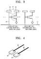
- FIG. 3illustrates a logic for forming a nanowire in a plurality of memory cells by using CMOS unit cells including a current monitor and a switching logic, as a system of controlling nanowire formation;
- FIGS. 4 through 6are perspective views illustrating examples of a nanowire memory device to which the method of fabricating a nanowire memory device according to the exemplary embodiment of the present invention is applicable.
- a method of fabricating a nanowire memory device(hereinafter, referred to as the ‘fabrication method’) and a system of controlling nanowire formation used in the fabrication method (hereinafter, referred to as the ‘system’) according to exemplary embodiments of the present invention will now be described more fully hereinafter with reference to the accompanying drawing.
- the fabrication method according to the present exemplary embodimentcomprises: forming electrodes spaced apart from each other, on a substrate; forming a nanowire between the electrodes by using a composite electric field; monitoring and controlling the nanowire formation to form only one nanowire between the electrodes while the nanowire is formed.
- FIG. 1illustrates an exemplary constitution of the system for monitoring and controlling the nanowire formation.
- a function generator 46applies power to first and second electrodes 40 and 42 formed on a substrate (not shown) and spaced apart from each other.
- a composite electric fieldis generated between the first and second electrodes 40 and 42 , and a nanowire 44 is formed between the first and second electrodes 40 and 42 .
- the nanowire 44may be a carbon nanotube or it may take other forms such as a carbon nanowire.
- the first electrode 40is directly connected with the function generator 46
- the second electrode 42is connected with the function generator 46 through a switching logic 50 and a current monitor 48 .
- the switching logic 50directly connected with the second electrode 42 cuts power supplied from the function generator 46 to the first and second electrodes 40 and 42 .
- the current monitor 48positioned between the function generator 46 and the switching logic 50 detects a point in time of the sudden increase of the current and sends a signal to the switching logic 50 .
- the switching logic 50receiving the signal from the current monitor 48 cuts the power supplied to the first and second electrodes 40 and 42 .
- the systemi.e., the power supplied to the first and second electrodes 40 and 42 , the current monitor 48 and the switching logic 50 , is constituted by using a CMOS circuit. Then, the power is independently supplied to the first electrode 40 and the second electrode 42 .
- CMOS circuitCMOS circuit
- the poweris independently supplied to the first electrode 40 and the second electrode 42 .
- the graph Gillustrates a change of the current flowing between the first and second electrodes 40 and 42 with the passage of time, before and after the nanowire 44 is formed between the first and second electrodes 40 and 42 .
- a first period P 1represents the current flowing between the first and second electrodes 40 and 42 before these electrodes 40 and 42 are connected by the nanowire 44
- a second period P 2represents the current flowing between the first and second electrodes 40 and 42 after these electrodes 40 and 42 are connected by the nanowire 44 and before the power is cut.
- FIG. 3illustrates a logic used the operation of the system, to form a nanowire in a plurality of memory cells by using a CMOS unit cell including a current monitor and a switching logic.
- each memory cell C 1power is applied from a function generator to each memory cell C 1 through a power bus L 1 .
- the power bus L 1is connected, in common, with a first electrode 40 of each memory cell C 1 .
- the power bus L 1is connected, in common, with a gate of each transistor T 1 corresponding to each memory cell C 1 .
- the number of transistorsis same as that of memory cells.
- the transistoris ON.
- a source of the transistor T 1is connected with the second electrode 42 , and a drain thereof is grounded.
- a CMOS unit cellis assigned between the first and second electrodes 40 and 42 .
- the CMOS unit cellincludes the current monitor and the switching logic which control the formation of the nanowire such that only a single nanowire is formed between the first and second electrodes 40 and 42 .
- the CMOS unit cellmay be positioned between a line L 2 branched off from the power bus L 1 to each memory cell C 1 and the drain of the transistor T 1 . Accordingly, the nanowire can be independently formed between the first and second electrodes 40 and 42 of each memory cell C 1 by the CMOS unit cell. When only the single nanowire is initially formed between the first and second electrodes 40 and 42 , it is possible to independently cut the power supplied to each memory cell C 1 .
- the CMOS unit cellmay further include a storing and reading logic used for storing and reading data in the memory cell C 1 .
- the design, manufacture and mass production of the logic as shown in FIG. 3are possible by using a semiconductor process.
- Nanowire memory devices formed by the fabrication method according to the present exemplary embodimentmay vary as shown, for example, in FIGS. 4 through 6 .
- a nanowire memory device of FIG. 4includes first and second electrodes 60 and 62 formed on a substrate (not shown) and spaced apart from each other.
- a first nanowire 64 formed by using a composite electric fieldis positioned, with a given length, on the first electrode 60 .
- a second nanowire 66 formed by using the composite electric fieldis positioned, with a given length, on the second elctrode 62 .
- the first and second nanowires 64 and 66are formed to be parallel to each other.
- the first and second nanowires 64 and 66may be, for example, carbon nanotubes or carbon nanowires, and have the same length.
- the first and second nanowires 64 and 66are used as a storage node where data 0 or 1 is stored.
- a first dummy electrode (not shown) corresponding to the first electrode 60 and a second dummy electrode (not shown) corresponding to the second electrode 62are formed on the substrate corresponding to the ends of the first and second nanowires 64 and 66 .
- the first nanowire 64is formed between the first electrode 60 and the first dummy electrode
- the second nanowire 66is formed between the second electrode 62 and the second dummy electrode.
- the first and second dummy electrodesare removed during a process of cutting the first and second nanowires 64 and 66 at the same regular length.
- the above-described nanowire formation systemis applied during the process of forming the first and second nanowires 64 and 66 , thereby forming only a single first nanowire 64 on the first electrode 60 and only a single second nanowire 66 on the second electrode 62 .
- a nanowire memory device as illustrated in FIG. 5includes first and second electrodes 70 and 72 formed on a substrate (not shown) and spaced apart from each other; and third and fourth electrodes 74 and 76 formed on the substrate and spaced apart from each other.
- the third electrode 74is paired with the first electrode 70
- the fourth electrode 76is paired with the second electrode 72 .
- the third and fourth electrodes 74 and 76are spaced apart from each other at the same interval as that of the first and second electrodes 70 and 72 .
- the first to fourth electrodes 70 , 72 , 74 and 76are positioned as shown in FIG. 5 .
- a first nanowire 78is formed between the first and third electrodes 70 and 74
- a second nanowire 80is formed between the second and fourth electrodes 72 and 76 .
- the first and second nanowires 78 and 80are formed by using a composite electric field. Only a single first nanowire 78 is formed between the first and third electrodes 70 and 74 , and only a single second nanowire 80 is formed between the second and fourth electrodes 72 and 76 , by using the system including the function generator 46 , the current monitor 48 and the switching logic 50 as described with reference to FIG. 1 .
- the first and second nanowires 78 and 80are used as a storage node.
- data 0or 1
- data 1or 0
- a memory device as illustrated in FIG. 6includes a substrate (not shown); a first electrode 90 formed on the substrate and insulated from the substrate; and a nanowire 92 formed at a given length. One end of the nanowire 92 is connected with the first electrode 90 . The nanowire 92 is formed to be parallel to the substrate. The nanowire 92 is used as a storage node, together with the substrate. Thus, depending on whether the other end of the nanowire 92 contacts with the substrate, it is considered that data 0 or 1 is recorded in the memory device.
- a dummy electrode(not shown) to be paired with the first electrode 90 is formed on a desired region of the substrate corresponding to the other end of the nanowire 92 . Then, the nanowire 92 is formed between the first electrode 90 and the dummy electrode. The nanowire 92 is formed by using a composite electric field. During a process of cutting the nanowire 92 at a regular length, the dummy electrode is removed.
- the systemis applied such that only a single nanowire 92 is formed between the first electrode 90 and the dummy electrode.
- the method of fabricating a nanowire memory deviceuses the system including the function generator for generating the composite electric field, the current monitor and the switching logic, during the process of forming the nanowire by using the composite electric field, thereby forming only the single nanowire between the electrodes to be paired.
- the present inventionis used to form the nanowire at an accurate position and to increase the effective operation yield of the memory device, i.e., the yield of the memory cells which are operable in accordance with predetermined operation conditions or standard operation conditions.
Landscapes
- Engineering & Computer Science (AREA)
- Chemical & Material Sciences (AREA)
- Nanotechnology (AREA)
- Aviation & Aerospace Engineering (AREA)
- Transportation (AREA)
- Mechanical Engineering (AREA)
- Physics & Mathematics (AREA)
- Mathematical Physics (AREA)
- Theoretical Computer Science (AREA)
- Crystallography & Structural Chemistry (AREA)
- Semiconductor Memories (AREA)
Abstract
Description
- This application claims priority from Korean Patent Application No. 10-2006-0022322, filed on Mar. 9, 2006, in the Korean Intellectual Property Office, the disclosure of which is incorporated herein in its entirety by reference.
- 1. Field of the Invention
- A method consistent with the present invention relates to a method of fabricating a semiconductor memory device and, more particularly, to a method of fabricating a memory device including a nanowire as a storage node and a system of controlling nanowire formation used in the same method.
- 2. Description of the Related Art
- Most of the recently introduced memory devices combine the advantages of existing volatile memory devices and those of existing non-volatile memory devices, for example, a ferroelectric RAM (FRAM), a magnetic RAM (MRAM), a phase change RAM (PRAM), or a resistive RAM (RRAM). The advanced memory devices such as the FRAM, MRAM, PRAM, and RRAM are different from one another in terms of the constitution of a storage node.
- As another example of the advanced memory devices, a memory device using a carbon nanotube has been introduced. The carbon nanotube memory device uses a carbon nanotube as a storage node.
- The carbon nanotube memory device has the advantage of reducing the volume of the storage node, compared to the FRAM, MRAM, PRAM, or RRAM. In the carbon nanotube memory device, since the carbon nanotube is formed by using a composite electric field, it is possible to form the carbon nanotube at an accurate position.
- However, in a method of fabricating the carbon nanotube memory device which has been introduced up to now, there may occur an occasion that two or more carbon nanotubes are formed between electrodes forming one cell, thereby decreasing an effective operation yield of the memory device.
- Exemplary embodiments consistent with the present invention provide a method of fabricating a nanowire memory device which is capable of increasing an effective operation yield.
- The present invention also provides a system of controlling nanowire formation used in the method of fabricating a nanowire memory device.
- According to an aspect of the invention, there is provided a method of fabricating a nanowire memory device which includes a substrate; an electrode formed on the substrate and insulated from the substrate; and a nanowire having its one end connected with the electrode and formed at a given length, the method comprising: forming an electrode and a dummy electrode to be paired with the electrode on the substrate; forming the nanowire between the electrode and the dummy electrode while measuring a current flowing between the electrode and the dummy electrode, and cutting power applied between the electrode and the dummy electrode when the current measured is a given value; and removing the dummy electrode.
- According to another aspect of the present invention, there is provided a method of fabricating a nanowire memory device which includes a substrate; two pairs of electrodes formed on the substrate, insulated from the substrate and spaced apart from each other, a nanowire connecting two electrodes of each pair, the method comprising: forming, on the substrate, two electrodes of a first pair spaced apart from each other, and two electrodes of a second pair spaced apart from each other, and spaced apart from the first pair of electrodes; and forming the nanowire between two electrodes of each pair while measuring a current flowing between the two electrodes of each pair, and cutting power applied between the two electrodes of each pair when the current measured is a given value.
- In the method, at least one more first pair of electrodes, at least one more second pair of electrodes, and at least one more nanowire for connecting two electrodes in each pair may be formed.
- The nanowire may be formed using a composite electric field, and the measuring of the current and the cutting of the power may be performed using a system including a switching logic and a current monitor. The system may be a complementary metal-oxide semiconductor (CMOS) logic.
- According to another aspect of the present invention, there is provided a system of controlling nanowire formation used in a method of fabricating a nanowire memory device which includes electrodes spaced apart from one another; and a nanowire for connecting two electrodes of each pair, among the electrodes, the system comprising: a function generator which generates a composite electric field between two electrodes to be paired; a current monitor which measures a current flowing between the two electrodes while the nanowire is formed, and sends an operation signal when the current measured is a given value; and a switching logic which cuts power applied between the two electrodes when the operation signal is given from the current monitor.
- According to another aspect of the present invention, there is provided a system of controlling nanowire formation used in a method of fabricating a nanowire memory device, in which the method comprises: forming an electrode and a dummy electrode of the electrode on a substrate; forming a nanowire between the electrode and the dummy electrode; and removing the dummy electrode, the system comprising: a function generator which generates a composite electric field between the electrode and the dummy electrode; a current monitor which measures a current flowing between the electrode and the dummy electrode while the nanowire is formed, and sends an operation signal when the measured current is a given value; and a switching logic which cuts power applied between the electrode and the dummy electrode when the operation signal is given from the current monitor.
- The systems may be a CMOS logic including the function generator, current monitor and switching logic.
- According to another aspect of the present invention, there is provided a system of controlling nanowire formation used in a method of fabricating a nanowire memory device which includes electrodes spaced apart from one another, and a nanowire connecting two electrodes to be paired among the electrodes, the system comprising: means for generating a composite electric field between the two electrodes to be paired, a current monitor which measures a current flowing between the two electrodes while the nanowire is formed, and sends an operation signal when the current measured is a given value; and a switching logic which cuts power applied between the two electrodes when the operation signal is given from the current monitor.
- In accordance with the present invention, the effective operation yield, i.e., the yield of an operable memory cell is increased.
- The above and other features and advantages of the present invention will become more apparent by describing in detail exemplary embodiments thereof with reference to the attached drawings, in which:
FIG. 1 is a block diagram illustrating constitution of a system for monitoring whether a nanowire is formed between electrodes, in a method of fabricating a nanowire memory device according to an exemplary embodiment of the present invention;FIG. 2 is a graph illustrating a change of the current-time characteristics before and after the nanowire is formed between the electrodes, in the method of fabricating a nanowire memory device according to the exemplary embodiment of the present invention;FIG. 3 illustrates a logic for forming a nanowire in a plurality of memory cells by using CMOS unit cells including a current monitor and a switching logic, as a system of controlling nanowire formation; andFIGS. 4 through 6 are perspective views illustrating examples of a nanowire memory device to which the method of fabricating a nanowire memory device according to the exemplary embodiment of the present invention is applicable.- A method of fabricating a nanowire memory device (hereinafter, referred to as the ‘fabrication method’) and a system of controlling nanowire formation used in the fabrication method (hereinafter, referred to as the ‘system’) according to exemplary embodiments of the present invention will now be described more fully hereinafter with reference to the accompanying drawing.
- In the drawings, the thickness of layers and regions is exaggerated for clarity.
- The description of the system will not be separately presented but will be presented along with the description of the fabrication method according to the present exemplary embodiment.
- The fabrication method according to the present exemplary embodiment comprises: forming electrodes spaced apart from each other, on a substrate; forming a nanowire between the electrodes by using a composite electric field; monitoring and controlling the nanowire formation to form only one nanowire between the electrodes while the nanowire is formed.
FIG. 1 illustrates an exemplary constitution of the system for monitoring and controlling the nanowire formation.- Referring to
FIG. 1 , afunction generator 46 applies power to first andsecond electrodes second electrodes nanowire 44 is formed between the first andsecond electrodes nanowire 44 may be a carbon nanotube or it may take other forms such as a carbon nanowire. Thefirst electrode 40 is directly connected with thefunction generator 46, and thesecond electrode 42 is connected with thefunction generator 46 through aswitching logic 50 and acurrent monitor 48. When thenanowire 44 is formed between the first andsecond electrodes second electrodes switching logic 50 directly connected with thesecond electrode 42 cuts power supplied from thefunction generator 46 to the first andsecond electrodes nanowire 44 is formed between the first andsecond electrodes second electrodes current monitor 48 positioned between thefunction generator 46 and theswitching logic 50 detects a point in time of the sudden increase of the current and sends a signal to theswitching logic 50. Theswitching logic 50 receiving the signal from thecurrent monitor 48 cuts the power supplied to the first andsecond electrodes second electrodes current monitor 48 and theswitching logic 50, is constituted by using a CMOS circuit. Then, the power is independently supplied to thefirst electrode 40 and thesecond electrode 42. When asingle nanowire 44 connecting thefirst electrode 40 with thesecond electrode 42 is formed between the first andsecond electrodes single nanowire 44 initially formed between the first andsecond electrodes - In
FIG. 2 , the graph G illustrates a change of the current flowing between the first andsecond electrodes nanowire 44 is formed between the first andsecond electrodes - In the graph G, a first period P1 represents the current flowing between the first and
second electrodes electrodes nanowire 44, and a second period P2 represents the current flowing between the first andsecond electrodes electrodes nanowire 44 and before the power is cut. - Referring to the graph G of
FIG. 2 , it is known that a change of the current is sudden between the first and second periods P1 and P2. The sudden change results from the connection of the first andsecond electrodes nanowire 44. Thecurrent monitor 48 detects the change of the current and informs theswitching logic 50 thereof. Thus, there is no current flowing between the first andsecond electrodes FIG. 3 illustrates a logic used the operation of the system, to form a nanowire in a plurality of memory cells by using a CMOS unit cell including a current monitor and a switching logic.- Referring to
FIG. 3 , power is applied from a function generator to each memory cell C1 through a power bus L1. The power bus L1 is connected, in common, with afirst electrode 40 of each memory cell C1. The power bus L1 is connected, in common, with a gate of each transistor T1 corresponding to each memory cell C1. The number of transistors is same as that of memory cells. When the power is supplied to thefirst electrode 40 through the power bus L1, the transistor is ON. A source of the transistor T1 is connected with thesecond electrode 42, and a drain thereof is grounded. In each memory cell C1, a CMOS unit cell is assigned between the first andsecond electrodes second electrodes second electrodes second electrodes - The design, manufacture and mass production of the logic as shown in
FIG. 3 are possible by using a semiconductor process. - Nanowire memory devices formed by the fabrication method according to the present exemplary embodiment may vary as shown, for example, in
FIGS. 4 through 6 . - A nanowire memory device of
FIG. 4 includes first andsecond electrodes first nanowire 64 formed by using a composite electric field is positioned, with a given length, on thefirst electrode 60. Asecond nanowire 66 formed by using the composite electric field is positioned, with a given length, on thesecond elctrode 62. The first andsecond nanowires second nanowires second nanowires second nanowires second electrodes second nanowires FIG. 4 , i.e., when the resistance between the first andsecond electrodes - In a method of fabricating the memory device as illustrated in
FIG. 4 , a first dummy electrode (not shown) corresponding to thefirst electrode 60 and a second dummy electrode (not shown) corresponding to thesecond electrode 62 are formed on the substrate corresponding to the ends of the first andsecond nanowires first nanowire 64 is formed between thefirst electrode 60 and the first dummy electrode, and thesecond nanowire 66 is formed between thesecond electrode 62 and the second dummy electrode. The first and second dummy electrodes are removed during a process of cutting the first andsecond nanowires - The above-described nanowire formation system is applied during the process of forming the first and
second nanowires first nanowire 64 on thefirst electrode 60 and only a singlesecond nanowire 66 on thesecond electrode 62. - A nanowire memory device as illustrated in
FIG. 5 includes first andsecond electrodes fourth electrodes third electrode 74 is paired with thefirst electrode 70, and thefourth electrode 76 is paired with thesecond electrode 72. The third andfourth electrodes second electrodes - The first to
fourth electrodes FIG. 5 . Afirst nanowire 78 is formed between the first andthird electrodes second nanowire 80 is formed between the second andfourth electrodes second nanowires first nanowire 78 is formed between the first andthird electrodes second nanowire 80 is formed between the second andfourth electrodes function generator 46, thecurrent monitor 48 and the switchinglogic 50 as described with reference toFIG. 1 . - In the memory device of
FIG. 5 , the first andsecond nanowires second nanowires second nanowires - A memory device as illustrated in
FIG. 6 includes a substrate (not shown); afirst electrode 90 formed on the substrate and insulated from the substrate; and ananowire 92 formed at a given length. One end of thenanowire 92 is connected with thefirst electrode 90. Thenanowire 92 is formed to be parallel to the substrate. Thenanowire 92 is used as a storage node, together with the substrate. Thus, depending on whether the other end of thenanowire 92 contacts with the substrate, it is considered that data0 or1 is recorded in the memory device. - In a method of fabricating the memory device of
FIG. 6 , before thenanowire 92 is formed, a dummy electrode (not shown) to be paired with thefirst electrode 90 is formed on a desired region of the substrate corresponding to the other end of thenanowire 92. Then, thenanowire 92 is formed between thefirst electrode 90 and the dummy electrode. Thenanowire 92 is formed by using a composite electric field. During a process of cutting thenanowire 92 at a regular length, the dummy electrode is removed. - During the process of forming the
nanowire 92, the system is applied such that only asingle nanowire 92 is formed between thefirst electrode 90 and the dummy electrode. - As described above, the method of fabricating a nanowire memory device according to the present embodiment uses the system including the function generator for generating the composite electric field, the current monitor and the switching logic, during the process of forming the nanowire by using the composite electric field, thereby forming only the single nanowire between the electrodes to be paired. Thus, the present invention is used to form the nanowire at an accurate position and to increase the effective operation yield of the memory device, i.e., the yield of the memory cells which are operable in accordance with predetermined operation conditions or standard operation conditions.
- While the present invention has been particularly shown and described with reference to an exemplary embodiment thereof, it should not be construed as being limited to the embodiment set forth, and it will be understood by those of ordinary skill in the art that various changes in form and details may be made. For example, a skilled person in the art may apply the above-described system to a method of fabricating a memory device having any other constitution if it uses a nanowire as a storage node, in addition to the memory devices illustrated in
FIGS. 4 through 6 . Thus, the spirit and scope of the present invention shall not be limited by the exemplary embodiments and shall be defined by the following claims.
Claims (13)
Applications Claiming Priority (2)
| Application Number | Priority Date | Filing Date | Title |
|---|---|---|---|
| KR10-2006-0022322 | 2006-03-09 | ||
| KR1020060022322AKR100745764B1 (en) | 2006-03-09 | 2006-03-09 | Manufacturing Method of Nanowire Memory Device and Nanowire Formation Control System Used in the Method |
Publications (2)
| Publication Number | Publication Date |
|---|---|
| US20070231988A1true US20070231988A1 (en) | 2007-10-04 |
| US7985646B2 US7985646B2 (en) | 2011-07-26 |
Family
ID=38559675
Family Applications (1)
| Application Number | Title | Priority Date | Filing Date |
|---|---|---|---|
| US11/712,990Expired - Fee RelatedUS7985646B2 (en) | 2006-03-09 | 2007-03-02 | Method of fabricating nanowire memory device and system of controlling nanowire formation used in the same |
Country Status (2)
| Country | Link |
|---|---|
| US (1) | US7985646B2 (en) |
| KR (1) | KR100745764B1 (en) |
Cited By (19)
| Publication number | Priority date | Publication date | Assignee | Title |
|---|---|---|---|---|
| US20070268739A1 (en)* | 2006-03-08 | 2007-11-22 | Samsung Electronics Co., Ltd. | Nanowire memory device and method of manufacturing the same |
| US20090250681A1 (en)* | 2008-04-08 | 2009-10-08 | John Smythe | Non-Volatile Resistive Oxide Memory Cells, Non-Volatile Resistive Oxide Memory Arrays, And Methods Of Forming Non-Volatile Resistive Oxide Memory Cells And Memory Arrays |
| US20100289509A1 (en)* | 2007-05-15 | 2010-11-18 | Samsung Electronics Co., Ltd. | Method for positioning carbon nanotubes between electrodes, biomolecule detector based on carbon nanotube-probe complexes and detection method using the same |
| US8134137B2 (en) | 2008-06-18 | 2012-03-13 | Micron Technology, Inc. | Memory device constructions, memory cell forming methods, and semiconductor construction forming methods |
| US8154906B2 (en) | 2008-01-15 | 2012-04-10 | Micron Technology, Inc. | Memory cells, memory cell programming methods, memory cell reading methods, memory cell operating methods, and memory devices |
| US8211743B2 (en) | 2008-05-02 | 2012-07-03 | Micron Technology, Inc. | Methods of forming non-volatile memory cells having multi-resistive state material between conductive electrodes |
| US8411477B2 (en) | 2010-04-22 | 2013-04-02 | Micron Technology, Inc. | Arrays of vertically stacked tiers of non-volatile cross point memory cells, methods of forming arrays of vertically stacked tiers of non-volatile cross point memory cells, and methods of reading a data value stored by an array of vertically stacked tiers of non-volatile cross point memory cells |
| US8427859B2 (en) | 2010-04-22 | 2013-04-23 | Micron Technology, Inc. | Arrays of vertically stacked tiers of non-volatile cross point memory cells, methods of forming arrays of vertically stacked tiers of non-volatile cross point memory cells, and methods of reading a data value stored by an array of vertically stacked tiers of non-volatile cross point memory cells |
| US8431458B2 (en) | 2010-12-27 | 2013-04-30 | Micron Technology, Inc. | Methods of forming a nonvolatile memory cell and methods of forming an array of nonvolatile memory cells |
| US8537592B2 (en) | 2011-04-15 | 2013-09-17 | Micron Technology, Inc. | Arrays of nonvolatile memory cells and methods of forming arrays of nonvolatile memory cells |
| US8681531B2 (en) | 2011-02-24 | 2014-03-25 | Micron Technology, Inc. | Memory cells, methods of forming memory cells, and methods of programming memory cells |
| US8753949B2 (en) | 2010-11-01 | 2014-06-17 | Micron Technology, Inc. | Nonvolatile memory cells and methods of forming nonvolatile memory cells |
| US8759809B2 (en) | 2010-10-21 | 2014-06-24 | Micron Technology, Inc. | Integrated circuitry comprising nonvolatile memory cells having platelike electrode and ion conductive material layer |
| US8791447B2 (en) | 2011-01-20 | 2014-07-29 | Micron Technology, Inc. | Arrays of nonvolatile memory cells and methods of forming arrays of nonvolatile memory cells |
| US8811063B2 (en) | 2010-11-01 | 2014-08-19 | Micron Technology, Inc. | Memory cells, methods of programming memory cells, and methods of forming memory cells |
| US8976566B2 (en) | 2010-09-29 | 2015-03-10 | Micron Technology, Inc. | Electronic devices, memory devices and memory arrays |
| US9343665B2 (en) | 2008-07-02 | 2016-05-17 | Micron Technology, Inc. | Methods of forming a non-volatile resistive oxide memory cell and methods of forming a non-volatile resistive oxide memory array |
| US9412421B2 (en) | 2010-06-07 | 2016-08-09 | Micron Technology, Inc. | Memory arrays |
| US9454997B2 (en) | 2010-12-02 | 2016-09-27 | Micron Technology, Inc. | Array of nonvolatile memory cells having at least five memory cells per unit cell, having a plurality of the unit cells which individually comprise three elevational regions of programmable material, and/or having a continuous volume having a combination of a plurality of vertically oriented memory cells and a plurality of horizontally oriented memory cells; array of vertically stacked tiers of nonvolatile memory cells |
Families Citing this family (2)
| Publication number | Priority date | Publication date | Assignee | Title |
|---|---|---|---|---|
| CN104779346B (en)* | 2014-01-15 | 2017-04-12 | 清华大学 | Preparation method of phase change storage unit |
| US10903425B2 (en) | 2018-09-05 | 2021-01-26 | International Business Machines Corporation | Oxygen vacancy and filament-loss protection for resistive switching devices |
Citations (6)
| Publication number | Priority date | Publication date | Assignee | Title |
|---|---|---|---|---|
| US6719602B2 (en)* | 2001-05-28 | 2004-04-13 | Yoshikazu Nakayama | Nanotube length control method |
| US6874668B2 (en)* | 2000-07-25 | 2005-04-05 | The Regents Of The University Of California | Telescoped multiwall nanotube and manufacture thereof |
| US7256063B2 (en)* | 2003-06-02 | 2007-08-14 | Ambient Systems, Inc. | Nanoelectromechanical transistors and switch systems |
| US20070268739A1 (en)* | 2006-03-08 | 2007-11-22 | Samsung Electronics Co., Ltd. | Nanowire memory device and method of manufacturing the same |
| US7382648B2 (en)* | 2004-09-30 | 2008-06-03 | California Institute Of Technology | Nanomechanical switching device |
| US7405420B1 (en)* | 2006-09-29 | 2008-07-29 | The Board Of Trustees Of The Leland Stanford Junior University | Method and system for chalcogenide-based nanowire memory |
Family Cites Families (2)
| Publication number | Priority date | Publication date | Assignee | Title |
|---|---|---|---|---|
| JP2005031228A (en)* | 2003-07-09 | 2005-02-03 | Fuji Xerox Co Ltd | Cleaning device and cleaning method for image forming apparatus |
| WO2005017967A2 (en)* | 2003-08-13 | 2005-02-24 | Nantero, Inc. | Nanotube device structure and methods of fabrication |
- 2006
- 2006-03-09KRKR1020060022322Apatent/KR100745764B1/ennot_activeExpired - Fee Related
- 2007
- 2007-03-02USUS11/712,990patent/US7985646B2/ennot_activeExpired - Fee Related
Patent Citations (6)
| Publication number | Priority date | Publication date | Assignee | Title |
|---|---|---|---|---|
| US6874668B2 (en)* | 2000-07-25 | 2005-04-05 | The Regents Of The University Of California | Telescoped multiwall nanotube and manufacture thereof |
| US6719602B2 (en)* | 2001-05-28 | 2004-04-13 | Yoshikazu Nakayama | Nanotube length control method |
| US7256063B2 (en)* | 2003-06-02 | 2007-08-14 | Ambient Systems, Inc. | Nanoelectromechanical transistors and switch systems |
| US7382648B2 (en)* | 2004-09-30 | 2008-06-03 | California Institute Of Technology | Nanomechanical switching device |
| US20070268739A1 (en)* | 2006-03-08 | 2007-11-22 | Samsung Electronics Co., Ltd. | Nanowire memory device and method of manufacturing the same |
| US7405420B1 (en)* | 2006-09-29 | 2008-07-29 | The Board Of Trustees Of The Leland Stanford Junior University | Method and system for chalcogenide-based nanowire memory |
Cited By (59)
| Publication number | Priority date | Publication date | Assignee | Title |
|---|---|---|---|---|
| US20070268739A1 (en)* | 2006-03-08 | 2007-11-22 | Samsung Electronics Co., Ltd. | Nanowire memory device and method of manufacturing the same |
| US8184473B2 (en) | 2006-03-08 | 2012-05-22 | Samsung Electronics Co., Ltd. | Nanowire memory device and method of manufacturing the same |
| US7821813B2 (en)* | 2006-03-08 | 2010-10-26 | Samsung Electronics Co., Ltd. | Nanowire memory device and method of manufacturing the same |
| US20100320564A1 (en)* | 2006-03-08 | 2010-12-23 | Samsung Electronics Co., Ltd. | Nanowire memory device and method of manufacturing the same |
| US8293654B2 (en) | 2006-03-08 | 2012-10-23 | Samsung Electronics Co., Ltd. | Nanowire memory device and method of manufacturing the same |
| US20100289509A1 (en)* | 2007-05-15 | 2010-11-18 | Samsung Electronics Co., Ltd. | Method for positioning carbon nanotubes between electrodes, biomolecule detector based on carbon nanotube-probe complexes and detection method using the same |
| US7928740B2 (en)* | 2007-05-15 | 2011-04-19 | Samsung Electronics Co., Ltd. | Method for positioning carbon nanotubes between electrodes, biomolecule detector based on carbon nanotube-probe complexes and detection method using the same |
| US9805792B2 (en) | 2008-01-15 | 2017-10-31 | Micron Technology, Inc. | Memory cells, memory cell programming methods, memory cell reading methods, memory cell operating methods, and memory devices |
| US8154906B2 (en) | 2008-01-15 | 2012-04-10 | Micron Technology, Inc. | Memory cells, memory cell programming methods, memory cell reading methods, memory cell operating methods, and memory devices |
| US11393530B2 (en) | 2008-01-15 | 2022-07-19 | Micron Technology, Inc. | Memory cells, memory cell programming methods, memory cell reading methods, memory cell operating methods, and memory devices |
| US9343145B2 (en) | 2008-01-15 | 2016-05-17 | Micron Technology, Inc. | Memory cells, memory cell programming methods, memory cell reading methods, memory cell operating methods, and memory devices |
| US10262734B2 (en) | 2008-01-15 | 2019-04-16 | Micron Technology, Inc. | Memory cells, memory cell programming methods, memory cell reading methods, memory cell operating methods, and memory devices |
| US10790020B2 (en) | 2008-01-15 | 2020-09-29 | Micron Technology, Inc. | Memory cells, memory cell programming methods, memory cell reading methods, memory cell operating methods, and memory devices |
| US20090250681A1 (en)* | 2008-04-08 | 2009-10-08 | John Smythe | Non-Volatile Resistive Oxide Memory Cells, Non-Volatile Resistive Oxide Memory Arrays, And Methods Of Forming Non-Volatile Resistive Oxide Memory Cells And Memory Arrays |
| US8034655B2 (en) | 2008-04-08 | 2011-10-11 | Micron Technology, Inc. | Non-volatile resistive oxide memory cells, non-volatile resistive oxide memory arrays, and methods of forming non-volatile resistive oxide memory cells and memory arrays |
| US8674336B2 (en) | 2008-04-08 | 2014-03-18 | Micron Technology, Inc. | Non-volatile resistive oxide memory cells, non-volatile resistive oxide memory arrays, and methods of forming non-volatile resistive oxide memory cells and memory arrays |
| US8211743B2 (en) | 2008-05-02 | 2012-07-03 | Micron Technology, Inc. | Methods of forming non-volatile memory cells having multi-resistive state material between conductive electrodes |
| US9577186B2 (en) | 2008-05-02 | 2017-02-21 | Micron Technology, Inc. | Non-volatile resistive oxide memory cells and methods of forming non-volatile resistive oxide memory cells |
| US9111788B2 (en) | 2008-06-18 | 2015-08-18 | Micron Technology, Inc. | Memory device constructions, memory cell forming methods, and semiconductor construction forming methods |
| US8134137B2 (en) | 2008-06-18 | 2012-03-13 | Micron Technology, Inc. | Memory device constructions, memory cell forming methods, and semiconductor construction forming methods |
| US9257430B2 (en) | 2008-06-18 | 2016-02-09 | Micron Technology, Inc. | Semiconductor construction forming methods |
| US9559301B2 (en) | 2008-06-18 | 2017-01-31 | Micron Technology, Inc. | Methods of forming memory device constructions, methods of forming memory cells, and methods of forming semiconductor constructions |
| US9666801B2 (en) | 2008-07-02 | 2017-05-30 | Micron Technology, Inc. | Methods of forming a non-volatile resistive oxide memory cell and methods of forming a non-volatile resistive oxide memory array |
| US9343665B2 (en) | 2008-07-02 | 2016-05-17 | Micron Technology, Inc. | Methods of forming a non-volatile resistive oxide memory cell and methods of forming a non-volatile resistive oxide memory array |
| US8542513B2 (en) | 2010-04-22 | 2013-09-24 | Micron Technology, Inc. | Arrays of vertically stacked tiers of non-volatile cross point memory cells, methods of forming arrays of vertically stacked tiers of non-volatile cross point memory cells, and methods of reading a data value stored by an array of vertically stacked tiers of non-volatile cross point memory cells |
| US8743589B2 (en) | 2010-04-22 | 2014-06-03 | Micron Technology, Inc. | Arrays of vertically stacked tiers of non-volatile cross point memory cells and methods of reading a data value stored by an array of vertically stacked tiers of non-volatile cross point memory cells |
| US8760910B2 (en) | 2010-04-22 | 2014-06-24 | Micron Technology, Inc. | Arrays of vertically stacked tiers of non-volatile cross point memory cells, methods of forming arrays of vertically stacked tiers of non-volatile cross point memory cells, and methods of reading a data value stored by an array of vertically stacked tiers of non-volatile cross point memory cells |
| US8411477B2 (en) | 2010-04-22 | 2013-04-02 | Micron Technology, Inc. | Arrays of vertically stacked tiers of non-volatile cross point memory cells, methods of forming arrays of vertically stacked tiers of non-volatile cross point memory cells, and methods of reading a data value stored by an array of vertically stacked tiers of non-volatile cross point memory cells |
| US8427859B2 (en) | 2010-04-22 | 2013-04-23 | Micron Technology, Inc. | Arrays of vertically stacked tiers of non-volatile cross point memory cells, methods of forming arrays of vertically stacked tiers of non-volatile cross point memory cells, and methods of reading a data value stored by an array of vertically stacked tiers of non-volatile cross point memory cells |
| US9036402B2 (en) | 2010-04-22 | 2015-05-19 | Micron Technology, Inc. | Arrays of vertically stacked tiers of non-volatile cross point memory cells |
| US10656231B1 (en) | 2010-06-07 | 2020-05-19 | Micron Technology, Inc. | Memory Arrays |
| US10241185B2 (en) | 2010-06-07 | 2019-03-26 | Micron Technology, Inc. | Memory arrays |
| US9697873B2 (en) | 2010-06-07 | 2017-07-04 | Micron Technology, Inc. | Memory arrays |
| US9989616B2 (en) | 2010-06-07 | 2018-06-05 | Micron Technology, Inc. | Memory arrays |
| US9887239B2 (en) | 2010-06-07 | 2018-02-06 | Micron Technology, Inc. | Memory arrays |
| US10613184B2 (en) | 2010-06-07 | 2020-04-07 | Micron Technology, Inc. | Memory arrays |
| US10746835B1 (en) | 2010-06-07 | 2020-08-18 | Micron Technology, Inc. | Memory arrays |
| US10859661B2 (en) | 2010-06-07 | 2020-12-08 | Micron Technology, Inc. | Memory arrays |
| US9412421B2 (en) | 2010-06-07 | 2016-08-09 | Micron Technology, Inc. | Memory arrays |
| US8976566B2 (en) | 2010-09-29 | 2015-03-10 | Micron Technology, Inc. | Electronic devices, memory devices and memory arrays |
| US8883604B2 (en) | 2010-10-21 | 2014-11-11 | Micron Technology, Inc. | Integrated circuitry comprising nonvolatile memory cells and methods of forming a nonvolatile memory cell |
| US8759809B2 (en) | 2010-10-21 | 2014-06-24 | Micron Technology, Inc. | Integrated circuitry comprising nonvolatile memory cells having platelike electrode and ion conductive material layer |
| US8811063B2 (en) | 2010-11-01 | 2014-08-19 | Micron Technology, Inc. | Memory cells, methods of programming memory cells, and methods of forming memory cells |
| US9406878B2 (en) | 2010-11-01 | 2016-08-02 | Micron Technology, Inc. | Resistive memory cells with two discrete layers of programmable material, methods of programming memory cells, and methods of forming memory cells |
| US9117998B2 (en) | 2010-11-01 | 2015-08-25 | Micron Technology, Inc. | Nonvolatile memory cells and methods of forming nonvolatile memory cells |
| US8796661B2 (en) | 2010-11-01 | 2014-08-05 | Micron Technology, Inc. | Nonvolatile memory cells and methods of forming nonvolatile memory cell |
| US8753949B2 (en) | 2010-11-01 | 2014-06-17 | Micron Technology, Inc. | Nonvolatile memory cells and methods of forming nonvolatile memory cells |
| US9454997B2 (en) | 2010-12-02 | 2016-09-27 | Micron Technology, Inc. | Array of nonvolatile memory cells having at least five memory cells per unit cell, having a plurality of the unit cells which individually comprise three elevational regions of programmable material, and/or having a continuous volume having a combination of a plurality of vertically oriented memory cells and a plurality of horizontally oriented memory cells; array of vertically stacked tiers of nonvolatile memory cells |
| US9034710B2 (en) | 2010-12-27 | 2015-05-19 | Micron Technology, Inc. | Methods of forming a nonvolatile memory cell and methods of forming an array of nonvolatile memory cells |
| US8652909B2 (en) | 2010-12-27 | 2014-02-18 | Micron Technology, Inc. | Methods of forming a nonvolatile memory cell and methods of forming an array of nonvolatile memory cells array of nonvolatile memory cells |
| US8431458B2 (en) | 2010-12-27 | 2013-04-30 | Micron Technology, Inc. | Methods of forming a nonvolatile memory cell and methods of forming an array of nonvolatile memory cells |
| US9093368B2 (en) | 2011-01-20 | 2015-07-28 | Micron Technology, Inc. | Nonvolatile memory cells and arrays of nonvolatile memory cells |
| US8791447B2 (en) | 2011-01-20 | 2014-07-29 | Micron Technology, Inc. | Arrays of nonvolatile memory cells and methods of forming arrays of nonvolatile memory cells |
| US9424920B2 (en) | 2011-02-24 | 2016-08-23 | Micron Technology, Inc. | Memory cells, methods of forming memory cells, and methods of programming memory cells |
| US9257648B2 (en) | 2011-02-24 | 2016-02-09 | Micron Technology, Inc. | Memory cells, methods of forming memory cells, and methods of programming memory cells |
| US8681531B2 (en) | 2011-02-24 | 2014-03-25 | Micron Technology, Inc. | Memory cells, methods of forming memory cells, and methods of programming memory cells |
| US9184385B2 (en) | 2011-04-15 | 2015-11-10 | Micron Technology, Inc. | Arrays of nonvolatile memory cells and methods of forming arrays of nonvolatile memory cells |
| US8854863B2 (en) | 2011-04-15 | 2014-10-07 | Micron Technology, Inc. | Arrays of nonvolatile memory cells and methods of forming arrays of nonvolatile memory cells |
| US8537592B2 (en) | 2011-04-15 | 2013-09-17 | Micron Technology, Inc. | Arrays of nonvolatile memory cells and methods of forming arrays of nonvolatile memory cells |
Also Published As
| Publication number | Publication date |
|---|---|
| US7985646B2 (en) | 2011-07-26 |
| KR100745764B1 (en) | 2007-08-02 |
Similar Documents
| Publication | Publication Date | Title |
|---|---|---|
| US7985646B2 (en) | Method of fabricating nanowire memory device and system of controlling nanowire formation used in the same | |
| TWI705319B (en) | Apparatuses and methods for generating programmable voltage reference | |
| JP5230955B2 (en) | Resistive memory element | |
| TWI728020B (en) | Circuit, method and device for configurable impedance array | |
| US8067815B2 (en) | Aluminum copper oxide based memory devices and methods for manufacture | |
| JP5058487B2 (en) | Phase change RAM operation method | |
| US10608175B2 (en) | Resistance change device having electrode disposed between resistance switching layer and ferroelectric layer | |
| JP2013534723A (en) | Composition of memory cell with resistive switching layer | |
| US8212621B2 (en) | Memristive programmable frequency source and method | |
| US8604457B2 (en) | Phase-change memory element | |
| TW201729210A (en) | Method of RRAM row forming | |
| KR100657958B1 (en) | Memory element with resistor nodes in series connection structure | |
| JP6021688B2 (en) | Semiconductor device and control method thereof | |
| JP2008219011A (en) | Reconfigurable circuit and programming method thereof | |
| US20090010040A1 (en) | Resistance change memory device | |
| KR20150122648A (en) | Resistive random access memory cells having variable switching characteristics | |
| CN103348472A (en) | Non-volatile storage element and non-volatile storage device | |
| DE112023000316T5 (en) | CROSSPOINT ARRAY UPDATE SCHEME | |
| US20150103579A1 (en) | Memory device, writing method, and reading method | |
| CN108346449B (en) | eFuse storage circuit | |
| US10153326B2 (en) | Memory device | |
| US20100124096A1 (en) | Electric element, switching element, memory element, switching method and memory method | |
| KR20160130468A (en) | Memristor devices with a thermally-insulating cladding | |
| US20110069540A1 (en) | Method of a phase-change memory programming | |
| JP2017037689A (en) | Semiconductor device and rewriting method for switch cell |
Legal Events
| Date | Code | Title | Description |
|---|---|---|---|
| AS | Assignment | Owner name:SEOUL NATIONAL UNIVERSITY INDUSTRY FOUNDATION, KOR Free format text:ASSIGNMENT OF ASSIGNORS INTEREST;ASSIGNORS:YOO, JIN-GYOO;KIM, CHEOL-SOON;LEE, JUNG-HOON;REEL/FRAME:019016/0859 Effective date:20070227 Owner name:SAMSUNG ELECTRONICS CO., LTD., KOREA, REPUBLIC OF Free format text:ASSIGNMENT OF ASSIGNORS INTEREST;ASSIGNORS:YOO, JIN-GYOO;KIM, CHEOL-SOON;LEE, JUNG-HOON;REEL/FRAME:019016/0859 Effective date:20070227 | |
| STCF | Information on status: patent grant | Free format text:PATENTED CASE | |
| FPAY | Fee payment | Year of fee payment:4 | |
| FEPP | Fee payment procedure | Free format text:PAYOR NUMBER ASSIGNED (ORIGINAL EVENT CODE: ASPN); ENTITY STATUS OF PATENT OWNER: LARGE ENTITY | |
| FEPP | Fee payment procedure | Free format text:MAINTENANCE FEE REMINDER MAILED (ORIGINAL EVENT CODE: REM.); ENTITY STATUS OF PATENT OWNER: LARGE ENTITY | |
| LAPS | Lapse for failure to pay maintenance fees | Free format text:PATENT EXPIRED FOR FAILURE TO PAY MAINTENANCE FEES (ORIGINAL EVENT CODE: EXP.); ENTITY STATUS OF PATENT OWNER: LARGE ENTITY | |
| STCH | Information on status: patent discontinuation | Free format text:PATENT EXPIRED DUE TO NONPAYMENT OF MAINTENANCE FEES UNDER 37 CFR 1.362 | |
| FP | Lapsed due to failure to pay maintenance fee | Effective date:20190726 |