US20070228589A1 - Method for expelling gas positioned between a substrate and a mold - Google Patents
Method for expelling gas positioned between a substrate and a moldDownload PDFInfo
- Publication number
- US20070228589A1 US20070228589A1US11/749,909US74990907AUS2007228589A1US 20070228589 A1US20070228589 A1US 20070228589A1US 74990907 AUS74990907 AUS 74990907AUS 2007228589 A1US2007228589 A1US 2007228589A1
- Authority
- US
- United States
- Prior art keywords
- substrate
- mold assembly
- region
- mold
- recited
- Prior art date
- Legal status (The legal status is an assumption and is not a legal conclusion. Google has not performed a legal analysis and makes no representation as to the accuracy of the status listed.)
- Granted
Links
Images


Classifications
- G—PHYSICS
- G03—PHOTOGRAPHY; CINEMATOGRAPHY; ANALOGOUS TECHNIQUES USING WAVES OTHER THAN OPTICAL WAVES; ELECTROGRAPHY; HOLOGRAPHY
- G03F—PHOTOMECHANICAL PRODUCTION OF TEXTURED OR PATTERNED SURFACES, e.g. FOR PRINTING, FOR PROCESSING OF SEMICONDUCTOR DEVICES; MATERIALS THEREFOR; ORIGINALS THEREFOR; APPARATUS SPECIALLY ADAPTED THEREFOR
- G03F7/00—Photomechanical, e.g. photolithographic, production of textured or patterned surfaces, e.g. printing surfaces; Materials therefor, e.g. comprising photoresists; Apparatus specially adapted therefor
- G03F7/0002—Lithographic processes using patterning methods other than those involving the exposure to radiation, e.g. by stamping
- B—PERFORMING OPERATIONS; TRANSPORTING
- B82—NANOTECHNOLOGY
- B82Y—SPECIFIC USES OR APPLICATIONS OF NANOSTRUCTURES; MEASUREMENT OR ANALYSIS OF NANOSTRUCTURES; MANUFACTURE OR TREATMENT OF NANOSTRUCTURES
- B82Y10/00—Nanotechnology for information processing, storage or transmission, e.g. quantum computing or single electron logic
- B—PERFORMING OPERATIONS; TRANSPORTING
- B82—NANOTECHNOLOGY
- B82Y—SPECIFIC USES OR APPLICATIONS OF NANOSTRUCTURES; MEASUREMENT OR ANALYSIS OF NANOSTRUCTURES; MANUFACTURE OR TREATMENT OF NANOSTRUCTURES
- B82Y40/00—Manufacture or treatment of nanostructures
Definitions
- the field of the inventionrelates generally to nano-fabrication of structures. More particularly, the present invention is directed to a method and a system of expelling gas positioned between a substrate and a mold.
- Nano-fabricationinvolves the fabrication of very small structures, e.g., having features on the order of nanometers or smaller.
- One area in which nano-fabrication has had a sizeable impactis in the processing of integrated circuits.
- nano-fabricationbecomes increasingly important. Nano-fabrication provides greater process control while allowing increased reduction of the minimum feature dimension of the structures formed.
- Other areas of development in which nano-fabrication has been employedinclude biotechnology, optical technology, mechanical systems and the like.
- An exemplary nano-fabrication techniqueis commonly referred to as imprint lithography.
- Exemplary imprint lithography processesare described in detail in numerous publications, such as United States patent application publication 2004/0065976 filed as U.S. patent application Ser. No. 10/264,960, entitled, “Method and a Mold to Arrange Features on a Substrate to Replicate Features having Minimal Dimensional Variability;” United States patent application publication 2004/0065252 filed as U.S. patent application Ser. No. 10/264,926, entitled “Method of Forming a Layer on a Substrate to Facilitate Fabrication of Metrology Standards;” and U.S. Pat. No. 6,936,194, entitled “Functional Patterning Material for Imprint Lithography Processes,” all of which are assigned to the assignee of the present invention.
- the fundamental imprint lithography technique disclosed in each of the aforementioned United States patent application publications and United States patentincludes formation of a relief pattern in a polymerizable layer and transferring a pattern corresponding to the relief pattern into an underlying substrate.
- the substratemay be positioned upon a motion stage to obtain a desired position to facilitate patterning thereof.
- a templateis employed spaced-apart from the substrate with a formable liquid present between the template and the substrate.
- the liquidis solidified to form a solidified layer that has a pattern recorded therein that is conforming to a shape of the surface of the template in contact with the liquid.
- the templateis then separated from the solidified layer such that the template and the substrate are spaced-apart.
- the substrate and the solidified layerare then subjected to processes to transfer, into the substrate, a relief image that corresponds to the pattern in the solidified layer.
- gasesmay be present between the template and the substrate and within the formable liquid which may result in, inter alia, pattern distortion of the solidified layer, low fidelity of features formed in the solidified layer, and a non-uniform thickness of a residual layer of the solidified layer, all of which are undesirable.
- FIG. 1is a simplified side view of a lithographic system having a patterning device spaced-apart from a substrate, the patterning device comprising a template and a mold;
- FIG. 2is a top down view of the substrate shown in FIG. 1 , the substrate having an inner, middle, and outer radius;
- FIG. 3is a side view of the substrate shown in FIG. 1 coupled to a substrate chuck;
- FIG. 4is a bottom-up plan view of the substrate chuck shown in FIG. 3
- FIG. 5is a top down view of the template shown in FIG. 1 , having a mold coupled thereto;
- FIG. 6is a side view of the template shown in FIG. 1 coupled to a template chuck;
- FIG. 7is a bottom-up plan view of the template chuck shown in FIG. 6 ;
- FIG. 8is a top down view showing an array of droplets of imprinting material positioned upon a region of the substrate shown in FIG. 1 ;
- FIG. 9is a simplified side view of the substrate shown in FIG. 1 , having a patterned layer positioned thereon;
- FIG. 10is a flow diagram showing a method of patterning the substrate shown in FIG. 1 , in a first embodiment
- FIG. 11is a side view of the patterning device shown in FIG. 1 having an altered shape
- FIG. 12is a side view of the patterning device shown in FIG. 11 , in contact with a portion of the droplets of imprinting material shown in FIG. 8 ;
- FIGS. 13-15are top down views showing the compression of the droplets shown in FIG. 8 , employing the altered shape of the template shown in FIG. 12 ;
- FIG. 16is a flow diagram showing a method of patterning a region of the substrate shown in FIG. 1 , in a second embodiment
- FIG. 17is a side view of the substrate shown in FIG. 1 having an altered shape
- FIG. 18is a side view of a pin exerting a force on the patterning device shown in FIG. 1 , to alter a shape thereof, and
- FIG. 19is a side view of the system shown in FIG. 1 , with a gas being introduced between the patterning device and the mold.
- Substrate 12may have circular shape; however, in a further embodiment, substrate 12 may have any geometric shape.
- substrate 12may have a disk shape having an inner radius r 1 and outer radius r 2 , with radius r 2 being greater than radius r 1 .
- inner radius r 1 and outer radius r 2is defined between inner radius r 1 and outer radius r 2 .
- middle radius r 3is defined between inner radius r 1 and outer radius r 2 .
- substrate 12may be coupled to a substrate chuck 14 .
- substrate chuck 14is a vacuum chuck, however, substrate chuck 14 may be any chuck including, but not limited to, vacuum, pin-type, groove-type, or electromagnetic, as described in U.S. Pat. No. 6,873,087 entitled “High-Precision Orientation Alignment and Gap Control Stages for Imprint Lithography Processes,” which is incorporated herein by reference.
- Substrate 12 and substrate chuck 14may be supported upon a stage 16 . Further, substrate 12 , substrate chuck 14 , and stage 16 may be positioned on a base (not shown). Stage 16 may provide motion about a first and a second axis, with the first and the second axis being orthogonal to one another, i.e., the x and y axes.
- substrate chuck 14includes first 18 and second 20 opposed sides.
- a side, or edge, surface 22extends between first side 18 and second side 20 .
- First side 18includes a first recess 20 , a second recess 22 , and a third recess 24 , defining first 26 , second 28 , third 30 , and fourth 32 spaced-apart support regions.
- First support region 26cinctures second 28 , third 30 , and fourth 32 support regions and first 20 , second 22 , and third 24 recesses.
- Second support region 28cinctures third 30 and fourth 32 support regions and second 22 and third 24 recesses.
- Third support region 30cinctures fourth support region 32 and third recess 24 .
- first 26 , second 28 , third 30 , and fourth 32 support regionsmay be formed from a compliant material.
- First 26 , second 28 , third 30 , and fourth 32 support regionsmay have a circular shape; however, in a further embodiment, first 26 , second 28 , third 30 , and fourth 32 may comprise any geometric shape desired.
- substrate chuck 12may comprise any number of throughways.
- Throughway 34places first and third recesses 20 and 24 in fluid communication with side surface 18 , however, in a further embodiment, it should be understood that throughway 34 may place first and third recesses 20 and 24 in fluid communication with any surface of substrate chuck 14 .
- Throughway 36places second recess 22 in fluid communication with side surface 18 , however, in a further embodiment, it should be understood that throughway 36 may place second recess 22 in fluid communication with any surface of substrate chuck 14 .
- throughway 34facilitates placing first 20 and third 24 recesses and throughway 36 facilitates placing second recesses 22 in fluid communication with a pressure control system, such as a pump system 38 .
- Pump system 38may include one or more pumps to control the pressure proximate to first 20 , second 22 , and third 24 recesses. To that end, when substrate 12 is coupled to substrate chuck 14 , substrate 12 rests against first 26 , second 28 , third 30 , and fourth 32 support regions, covering first 20 , second 22 , and third 24 recesses. First recess 20 and a portion 40 a of substrate 12 in superimposition therewith define a first chamber 42 . Second recess 22 and a portion 40 b of substrate 12 in superimposition therewith define a second chamber 44 . Third recesses 24 and a portion 40 c of substrate 12 in superimposition therewith define a third chamber 46 . Pump system 38 operates to control a pressure in first 42 , second 44 , and third 46 chambers.
- Patterning device 48spaced-apart from substrate 12 is a patterning device 48 .
- Patterning device 48comprises a template 50 having a mesa 52 extending therefrom towards substrate 12 with a patterning surface 54 thereon.
- mesa 52may be referred to as a mold 52 .
- template 50may be substantially absent of mold 52 .
- Template 50 and/or mold 52may be formed from such materials including but not limited to, fused-silica, quartz, silicon, organic polymers, siloxane polymers, borosilicate glass, fluorocarbon polymers, metal, and hardened sapphire.
- patterning surface 54comprises features defined by a plurality of spaced-apart recesses 56 and protrusions 58 .
- patterning surface 54may be substantially smooth and/or planar. Patterning surface 54 may define an original pattern that forms the basis of a pattern to be formed on substrate 12 .
- template 50may be coupled to a template chuck 60 , template chuck 60 being any chuck including, but not limited to, vacuum, pin-type, groove-type, or electromagnetic, as described in U.S. Pat. No. 6,873,087 entitled “High-Precision Orientation Alignment and Gap Control Stages for Imprint Lithography Processes”.
- Template chuck 60includes first 62 and second 64 opposed sides. A side, or edge, surface 66 extends between first side 62 and second side 64 .
- First side 62includes a first recess 68 , a second recess 70 , and a third recess 72 , defining first 74 , second 76 , and third 78 spaced-apart support regions.
- First support region 74cinctures second 70 and third 72 support regions and first 68 , second 70 , and third 72 recesses.
- Second support region 76cinctures third support region 78 and second 70 and third 72 recesses.
- Third support region 78cinctures third recess 72 .
- first 74 , second 76 , and third 78 support regionsmay be formed from a compliant material.
- First 74 , second 76 , and third 78 support regionsmay have a circular shape; however, in a further embodiment, first 74 , second 76 , and third 78 support regions may have any geometric shape desired.
- template chuck 60may comprise any number of throughways.
- Throughway 80places first and third recesses 68 and 72 in fluid communication with second side 64 , however, in a further embodiment, it should be understood that throughway 80 may place first and third recesses 68 and 72 in fluid communication with any surface of template chuck 60 .
- Throughway 82places second recess 70 in fluid communication with second side 64 , however, in a further embodiment, it should be understood that throughway 80 may place second recess 70 in fluid communication with any surface of template chuck 60 .
- throughway 80facilitates placing first 68 and third 72 recesses and throughway 82 facilitates placing second recesses 70 in fluid communication with a pressure control system, such as a pump system 84 .
- Pump system 84may include one or more pumps to control the pressure proximate to first 68 , second 70 , and third 72 recesses. To that end, when template 50 is coupled to template chuck 60 , template 50 rests against first 74 , second 76 , and third 78 support regions, covering first 68 , second 70 , and third 72 recesses. First recess 68 and a portion 86 a of template 50 in superimposition therewith define a first chamber 88 . Second recess 70 and a portion 86 b of template 50 in superimposition therewith define a second chamber 92 . Third recess 72 and a portion 86 c of substrate 12 in superimposition therewith define a third chamber 96 . Pump system 84 operates to control a pressure in first 88 , second 92 , and third 96 chambers. Further, template chuck 60 may be coupled to an imprint head 97 to facilitate movement of patterning device 48 .
- system 10further comprises a fluid dispense system 98 .
- Fluid dispense system 98may be in fluid communication with substrate 12 so as to deposit polymeric material 100 thereon.
- Fluid dispense system 98may comprise a plurality of dispensing units therein.
- polymeric material 100may be deposited using any known technique, e.g., drop dispense, spin-coating, dip coating, chemical vapor deposition (CVD), physical vapor deposition (PVD), thin film deposition, thick film deposition, and the like.
- CVDchemical vapor deposition
- PVDphysical vapor deposition
- polymeric material 100may be disposed upon substrate 12 before the desired volume is defined between mold 52 and substrate 12 . However, polymeric material 100 may fill the volume after the desired volume has been obtained. As shown in FIG.
- polymeric material 100may be deposited upon substrate 12 as a plurality of spaced-apart droplets 102 , defining a matrix array 104 .
- each droplet of droplets 102may have a unit volume of approximately 1-10 pico-liters.
- Droplets 102may be arranged in any two-dimensional arrangement on substrate 12 .
- system 10further comprises a source 106 of energy 108 coupled to direct energy 108 along a path 110 .
- Imprint head 97 and stage 16are configured to arrange mold 52 and substrate 12 , respectively, to be in superimposition and disposed in path 110 . Either imprint head 97 , stage 16 , or both vary a distance between mold 52 and substrate 12 to define a desired volume therebetween that is filled by polymeric material 100 .
- source 106produces energy 108 , e.g., broadband ultraviolet radiation that causes polymeric material 100 to solidify and/or cross-link conforming to the shape of a surface 112 of substrate 12 and patterning surface 54 , defining a patterned layer 114 on substrate 12 .
- Patterned layer 114may comprise a residual layer 116 and a plurality of features shown as protrusions 118 and recessions 120 . Control of this process is regulated by a processor 122 that is in data communication with stage 16 , pump systems 38 and 84 , imprint head 97 , fluid dispense system 98 , and source 106 , operating on a computer readable program stored in a memory 124 .
- system 10further includes a pin 126 coupled to stage 16 .
- Pin 126may translate about a third axis orthogonal to the first and second axis, i.e., along the z axis. As a result, pin 126 may contact mold 52 to alter a shape thereof, described further below.
- Pin 126may be any force or displacement actuator known in the art including, inter alia, pneumatic, piezoelectric, magnetostrictive, linear, and voice coils.
- pin 126may be a high resolution pressure regulator and clean series air piston, with a center pin thereof comprising a vacuum source that may evacuate an atmosphere between an interface of patterning device 48 and substrate 12 .
- a distance between mold 52 and substrate 12is varied such that a desired volume is defined therebetween that is filled by polymeric material 100 . Furthermore, after solidification, polymeric material 100 conforms to the shape of surface 112 of substrate 12 and patterning surface 54 , defining patterned layer 114 on substrate 12 . To that end, in a volume 128 defined between droplets 102 of matrix array 104 , there are gases present, and droplets 102 in matrix array 104 are spread over substrate 12 so as to avoid, if not prevent, trapping of gases and/or gas pockets between substrate 12 and mold 52 and within patterned layer 114 .
- the gases and/or gas pocketsmay be such gases including, but not limited to air, nitrogen, carbon dioxide, and helium.
- Gas and/or gas pockets between substrate 12 and mold 52 and within patterned layer 114may result in, inter alia, pattern distortion of features formed in patterned layer 114 , low fidelity of features formed in patterned layer 114 , and a non-uniform thickness of residual layer 116 across patterned layer 114 , all of which are undesirable.
- a method and a system of minimizing, if not preventing, trapping of gas and/or gas pockets between substrate 12 and mold 52 and within patterned layer 114are described below.
- polymeric material 100may be positioned on substrate 12 by drop dispense, spin-coating, dip coating, chemical vapor deposition (CVD), physical vapor deposition (PVD), thin film deposition, thick film deposition, and the like.
- polymeric material 100may be positioned on mold 52 .
- a shape of patterning device 48may be altered. More specifically, a shape of patterning device 48 may be altered such that a distance d 1 defined between mold 52 and substrate 12 at middle radius r 3 of substrate 12 , shown in FIG. 2 , is less than a distance defined between mold 52 and substrate 12 at remaining portions of mold 52 . In an example, distance d 1 is less than a distance d 2 , distance d 2 being defined at an edge of mold 52 . In a further embodiment, the distance d 1 may be defined at any desired location of mold 52 .
- the shape of patterning device 48may be altered by controlling a pressure within first and third chambers 68 and 72 .
- pump system 84operates to control the pressure in first and third chambers 68 and 72 .
- pump system 84may create a vacuum within first and third chambers 68 and 72 via throughway 80 such that portions 86 a and 86 c of template 50 may bow away from substrate 12 and bow towards template chuck 60 .
- portion 86 b of template 50bows toward substrate 12 and away from template chuck 60 .
- either imprint head 97shown in FIG. 1 , stage 16 , or both, may vary distance d 1 , shown in FIG. 11 , such that a portion of mold 52 contacts a sub-portion of droplets 102 .
- a portion of mold 52 in superimposition with middle radius r 3 of substrate 12shown in FIG. 2 , contacts a sub-portion of droplets 102 prior to the remaining portions of mold 52 contacting the remaining droplets of droplets 102 .
- any portion of mold 52may contact droplets 102 prior to remaining portions of mold 52 .
- mold 52contacts all of droplets 102 in superimposition with middle radius r 3 of substrate 12 , shown in FIG. 2 , substantially concurrently.
- Thiscauses droplets 102 to spread and to produce a contiguous liquid sheet 130 of polymeric material 100 .
- Edge 132 of liquid sheet 130defines a liquid-gas interface 134 that functions to push gases in volume 128 toward edge 136 of substrate 12 .
- Volume 128 between droplets 102define gas passages through which gas may be pushed to edge 136 .
- liquid-gas interface 134in conjunction with the gas passages reduces, if not prevents, trapping of gases in liquid sheet 130 .
- the shape of patterning device 48may be altered such that the desired volume defined between mold 52 and substrate 12 may be filled by polymeric material 100 , as described above with respect to FIG. 1 . More specifically, the shape of patterning device 48 may be altered by the combination of controlling the pressure within first and third chambers 88 and 96 and a force exerted by imprint head 97 , shown in FIG. 1 , and/or stage 16 upon patterning device 48 as a result of contact been polymeric material 100 and mold 52 . More specifically, as mentioned above, pump system 84 operates to control the pressure in first and third chambers 88 and 96 .
- pump system 84decreases a magnitude of the vacuum created within first and third chambers 88 and 96 via throughway 80 such that polymeric material 100 associated with subsequent subsets of droplets 100 surrounding middle radius r 3 of substrate 12 shown in FIG. 2 , spread to become included in contiguous fluid sheet 130 , as shown in FIG. 14 .
- the shape of patterning device 48continues to be altered such that mold 52 subsequently comes into contact with the remaining droplets 102 so that polymeric material 100 associated therewith spreads to become included in contiguous sheet 130 , as shown in FIG. 15 .
- interface 134has moved towards edge 136 so that there is an unimpeded path for the gases in the remaining volume 128 , shown in FIG. 8 , to travel thereto.
- a pressure within second chamber 92may be controlled. More specifically, as mentioned above, pump system 84 operates to control the pressure in second chamber 92 . To that end, pump system 84 may create a pressure within second chamber 92 via throughway 82 such that portion 86 c of template 50 may bow towards substrate 12 and bow away from template chuck 60 . Further, a pressure may be created within second chamber 92 concurrently with creating a vacuum in first and third chamber 88 and 96 , as mentioned above.
- polymeric material 100may be then be solidified and/or cross-linked, defining patterned layer 114 , shown in FIG. 9 .
- mold 52may be separated from patterned layer 114 , shown in FIG. 9 .
- polymeric material 100may be positioned on substrate 12 or mold 52 .
- a shape of patterning device 48may be altered. Furthermore, concurrently with altering a shape of patterning device 48 , a shape of substrate 12 may be altered. More specifically, a shape of substrate 12 may be altered by controlling a pressure within first and third chambers 42 and 46 . More specifically, as mentioned above, pump system 38 operates to control the pressure in first and third chambers 42 and 46 .
- pump system 38may create a vacuum within first and third chambers 42 and 46 via throughway 36 such that portions 40 a and 40 c of substrate 12 may bow away from substrate chuck 14 and bow towards mold 52 , as shown in FIG. 17 .
- portion 40 b of substrate 12bows toward mold 52 and away from substrate chuck 14 .
- analaogus to that mentioned above with respect to step 204shown in FIG. 10
- imprint head 97 , stage 16 , or bothmay vary distance d 1 , shown in FIG. 11 , such that a portion of mold 52 contacts a sub-portion of droplets 102 in superimposition with middle radius r 3 of substrate 12 , shown in FIG. 2 , substantially concurrently, producing contiguous liquid sheet 130 of polymeric material 100 .
- the shape of patterning device 48may be altered such that the desired volume defined between mold 52 and substrate 12 may be filled by polymeric material 100 . Furthermore, concurrently with altering the shape of patterning device 48 , the shape of substrate 12 may be altered. More specifically, as mentioned above, pump system 38 operates to control the pressure in first and third chambers 42 and 26 . To that end, pump system 38 decreases a magnitude of the vacuum created within first and third chambers 42 and 46 via throughway 36 concurrently with altering a shape of patterning device 48 as mentioned above in step 204 , shown in FIG.
- the shape of substrate 12may be further altered concurrently with the shape of patterning device 48 being altered such that mold 52 subsequently comes into contact with the remaining droplets 102 so that polymeric material 100 associated therewith spreads to become included in contiguous sheet 130 , as shown in FIG. 15 .
- the gases in volume 128shown in FIG. 8 may egress from between mold 52 and substrate 12 vis-à-vis edge 136 in substantially the same method as mentioned above with respect to step 206 , shown in FIG. 10 .
- a pressure within second chamber 44may be controlled. More specifically, as mentioned above, pump system 38 operates to control the pressure in second chamber 44 . To that end, pump system 38 may create a pressure within second chamber 44 via throughway 34 such that portion 40 b of template 50 may bow towards mold 52 and bow away from substrate chuck 14 . Further, a pressure may be created within second chamber 44 concurrently with creating a vacuum in first and third chamber 42 and 46 , as mentioned above.
- polymeric material 100may be then be solidified and/or cross-linked, defining patterned layer 114 , shown in FIG. 9 .
- mold 52may be separated from patterned layer 114 , shown in FIG. 9 .
- pin 126may be employed. More specifically, pin 126 may exert a force upon patterning device 48 , and in the present example, upon third portion 86 c of template 50 . As a result, patterning device 48 may comprise the aforementioned desired altered shape and may be employed in any of the methods mentioned above. Pin 126 may be also employed to facilitate separation of mold 52 and substrate 12 , as mentioned above with respect to steps 208 and 308 , shown in FIGS. 10 and 16 , respectively. Furthermore, after formation of patterned layer 114 , shown in FIG. 9 , pin 126 may translate away from patterned device 48 such that patterning device 48 may be substantially flat. Pin 126 may be in communication with processor 122 such that pin 126 may employ force feedback to determine a magnitude of the force.
- a gas 148may be introduced between substrate 12 and mold 52 via pin 126 .
- pin 126may comprise a throughway 150 having apertures 152 in fluid communication with a pressure control system, such as a pump system 38 .
- pin 126may comprise any number of apertures.
- Apertures 152may be positioned to introduce gas 148 between mold 52 and substrate 12 .
- Gas 148exerts a force upon mold 52 and substrate 12 to push mold 52 in a direction away from substrate 12 and to push substrate 12 in a direction away from mold 52 .
- gas 148may be introduced between mold 52 and substrate 12 when pin 126 is proximate to template 50 ; however, in a further embodiment, gas 148 may be introduced between mold 52 and substrate 12 when pin 126 is in any position.
Landscapes
- Engineering & Computer Science (AREA)
- Chemical & Material Sciences (AREA)
- Nanotechnology (AREA)
- Physics & Mathematics (AREA)
- General Physics & Mathematics (AREA)
- Crystallography & Structural Chemistry (AREA)
- Condensed Matter Physics & Semiconductors (AREA)
- Manufacturing & Machinery (AREA)
- Mathematical Physics (AREA)
- Theoretical Computer Science (AREA)
- Shaping Of Tube Ends By Bending Or Straightening (AREA)
- Exposure Of Semiconductors, Excluding Electron Or Ion Beam Exposure (AREA)
Abstract
Description
- The present application claims priority to U.S. Provisional Application No. 60/801,265, filed on May 18, 2006, entitled “Substrate Holding Apparatus and Methods for Data Storage Substrate” and U.S. Provisional Application No. 60/827,128, filed on Sep. 27, 2006, entitled “Double Side Imprinting”; and is a continuation-in-part of U.S. patent application Ser. No. 11/565,393, filed on Nov. 30, 2006, entitled “Method for Expelling Gas Positioned Between a Substrate and a Mold,” which claims priority to U.S. Provisional Application No. 60/748,380, filed on Dec. 8, 2005, entitled “Method and Apparatus for Imprinting with Preshaped Templates and/or Light Curable Liquids” and is a continuation of U.S. patent application Ser. No. 11/389,731, filed on Mar. 27, 2006, entitled “Imprint Lithography Substrate Processing Tool for Modulating Shapes of Substrates,” which is a continuation of U.S. patent application Ser. No. 10/293,224, now U.S. Pat. No. 7,019,819, filed on Nov. 13, 2002, entitled “Chucking System for Modulating Shapes of Substrates,” all of which are incorporated herein by reference.
- The field of the invention relates generally to nano-fabrication of structures. More particularly, the present invention is directed to a method and a system of expelling gas positioned between a substrate and a mold.
- Nano-fabrication involves the fabrication of very small structures, e.g., having features on the order of nanometers or smaller. One area in which nano-fabrication has had a sizeable impact is in the processing of integrated circuits. As the semiconductor processing industry continues to strive for larger production yields while increasing the circuits per unit area formed on a substrate, nano-fabrication becomes increasingly important. Nano-fabrication provides greater process control while allowing increased reduction of the minimum feature dimension of the structures formed. Other areas of development in which nano-fabrication has been employed include biotechnology, optical technology, mechanical systems and the like.
- An exemplary nano-fabrication technique is commonly referred to as imprint lithography. Exemplary imprint lithography processes are described in detail in numerous publications, such as United States patent application publication 2004/0065976 filed as U.S. patent application Ser. No. 10/264,960, entitled, “Method and a Mold to Arrange Features on a Substrate to Replicate Features having Minimal Dimensional Variability;” United States patent application publication 2004/0065252 filed as U.S. patent application Ser. No. 10/264,926, entitled “Method of Forming a Layer on a Substrate to Facilitate Fabrication of Metrology Standards;” and U.S. Pat. No. 6,936,194, entitled “Functional Patterning Material for Imprint Lithography Processes,” all of which are assigned to the assignee of the present invention.
- The fundamental imprint lithography technique disclosed in each of the aforementioned United States patent application publications and United States patent includes formation of a relief pattern in a polymerizable layer and transferring a pattern corresponding to the relief pattern into an underlying substrate. The substrate may be positioned upon a motion stage to obtain a desired position to facilitate patterning thereof. To that end, a template is employed spaced-apart from the substrate with a formable liquid present between the template and the substrate. The liquid is solidified to form a solidified layer that has a pattern recorded therein that is conforming to a shape of the surface of the template in contact with the liquid. The template is then separated from the solidified layer such that the template and the substrate are spaced-apart. The substrate and the solidified layer are then subjected to processes to transfer, into the substrate, a relief image that corresponds to the pattern in the solidified layer.
- To that end, gases may be present between the template and the substrate and within the formable liquid which may result in, inter alia, pattern distortion of the solidified layer, low fidelity of features formed in the solidified layer, and a non-uniform thickness of a residual layer of the solidified layer, all of which are undesirable. To that end, a need exists, therefore, to provide a method and a system to expel gas positioned between a substrate and a mold.
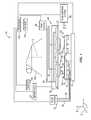
FIG. 1 is a simplified side view of a lithographic system having a patterning device spaced-apart from a substrate, the patterning device comprising a template and a mold;FIG. 2 is a top down view of the substrate shown inFIG. 1 , the substrate having an inner, middle, and outer radius;FIG. 3 is a side view of the substrate shown inFIG. 1 coupled to a substrate chuck;FIG. 4 is a bottom-up plan view of the substrate chuck shown inFIG. 3 FIG. 5 is a top down view of the template shown inFIG. 1 , having a mold coupled thereto;FIG. 6 is a side view of the template shown inFIG. 1 coupled to a template chuck;FIG. 7 is a bottom-up plan view of the template chuck shown inFIG. 6 ;FIG. 8 is a top down view showing an array of droplets of imprinting material positioned upon a region of the substrate shown inFIG. 1 ;FIG. 9 is a simplified side view of the substrate shown inFIG. 1 , having a patterned layer positioned thereon;FIG. 10 is a flow diagram showing a method of patterning the substrate shown inFIG. 1 , in a first embodiment;FIG. 11 is a side view of the patterning device shown inFIG. 1 having an altered shape;FIG. 12 is a side view of the patterning device shown inFIG. 11 , in contact with a portion of the droplets of imprinting material shown inFIG. 8 ;FIGS. 13-15 are top down views showing the compression of the droplets shown inFIG. 8 , employing the altered shape of the template shown inFIG. 12 ;FIG. 16 is a flow diagram showing a method of patterning a region of the substrate shown inFIG. 1 , in a second embodiment;FIG. 17 is a side view of the substrate shown inFIG. 1 having an altered shape;FIG. 18 is a side view of a pin exerting a force on the patterning device shown inFIG. 1 , to alter a shape thereof, andFIG. 19 is a side view of the system shown inFIG. 1 , with a gas being introduced between the patterning device and the mold.- Referring to
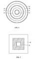
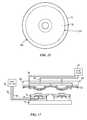
FIGS. 1 and 2 , asystem 10 to form a relief pattern on asubstrate 12 is shown.Substrate 12 may have circular shape; however, in a further embodiment,substrate 12 may have any geometric shape. In the present example,substrate 12 may have a disk shape having an inner radius r1and outer radius r2, with radius r2being greater than radius r1. Further, defined between inner radius r1and outer radius r2is a middle radius r3, with middle radius r3positioned substantially equidistant from inner radius r1and outer radius r2. - Referring to
FIG. 1 ,substrate 12 may be coupled to asubstrate chuck 14. As shownsubstrate chuck 14 is a vacuum chuck, however,substrate chuck 14 may be any chuck including, but not limited to, vacuum, pin-type, groove-type, or electromagnetic, as described in U.S. Pat. No. 6,873,087 entitled “High-Precision Orientation Alignment and Gap Control Stages for Imprint Lithography Processes,” which is incorporated herein by reference.Substrate 12 andsubstrate chuck 14 may be supported upon astage 16. Further,substrate 12,substrate chuck 14, andstage 16 may be positioned on a base (not shown).Stage 16 may provide motion about a first and a second axis, with the first and the second axis being orthogonal to one another, i.e., the x and y axes. - Referring to
FIGS. 1, 3 , and4,substrate chuck 14 includes first18 and second20 opposed sides. A side, or edge,surface 22 extends betweenfirst side 18 andsecond side 20.First side 18 includes afirst recess 20, asecond recess 22, and athird recess 24, defining first26, second28, third30, and fourth32 spaced-apart support regions.First support region 26cinctures second 28, third30, and fourth32 support regions and first20, second22, and third24 recesses.Second support region 28 cinctures third30 and fourth32 support regions and second22 and third24 recesses.Third support region 30 cincturesfourth support region 32 andthird recess 24.Third recess 24 cincturesfourth support region 32. In a further embodiment, first26,second 28, third30, and fourth32 support regions may be formed from a compliant material. First26, second28, third30, and fourth32 support regions may have a circular shape; however, in a further embodiment, first26, second28, third30, and fourth32 may comprise any geometric shape desired. - Formed in
substrate chuck 14 arethroughways substrate chuck 12 may comprise any number of throughways.Throughway 34 places first andthird recesses side surface 18, however, in a further embodiment, it should be understood thatthroughway 34 may place first andthird recesses substrate chuck 14.Throughway 36 placessecond recess 22 in fluid communication withside surface 18, however, in a further embodiment, it should be understood thatthroughway 36 may placesecond recess 22 in fluid communication with any surface ofsubstrate chuck 14. Furthermore, what is desired is thatthroughway 34 facilitates placing first20 and third24 recesses andthroughway 36 facilitates placingsecond recesses 22 in fluid communication with a pressure control system, such as apump system 38. Pump system 38 may include one or more pumps to control the pressure proximate to first20, second22, and third24 recesses. To that end, whensubstrate 12 is coupled tosubstrate chuck 14,substrate 12 rests against first26, second28, third30, and fourth32 support regions, covering first20, second22, and third24 recesses.First recess 20 and aportion 40aofsubstrate 12 in superimposition therewith define afirst chamber 42.Second recess 22 and aportion 40bofsubstrate 12 in superimposition therewith define asecond chamber 44. Third recesses24 and aportion 40cofsubstrate 12 in superimposition therewith define athird chamber 46.Pump system 38 operates to control a pressure in first42, second44, and third46 chambers.- Referring to
FIGS. 1 and 5 , spaced-apart fromsubstrate 12 is apatterning device 48.Patterning device 48 comprises atemplate 50 having amesa 52 extending therefrom towardssubstrate 12 with apatterning surface 54 thereon. Further,mesa 52 may be referred to as amold 52. In a further embodiment,template 50 may be substantially absent ofmold 52.Template 50 and/ormold 52 may be formed from such materials including but not limited to, fused-silica, quartz, silicon, organic polymers, siloxane polymers, borosilicate glass, fluorocarbon polymers, metal, and hardened sapphire. As shown, patterningsurface 54 comprises features defined by a plurality of spaced-apart recesses56 andprotrusions 58. However, in a further embodiment, patterningsurface 54 may be substantially smooth and/or planar. Patterningsurface 54 may define an original pattern that forms the basis of a pattern to be formed onsubstrate 12. - Referring to
FIGS. 1, 6 , and7,template 50 may be coupled to atemplate chuck 60,template chuck 60 being any chuck including, but not limited to, vacuum, pin-type, groove-type, or electromagnetic, as described in U.S. Pat. No. 6,873,087 entitled “High-Precision Orientation Alignment and Gap Control Stages for Imprint Lithography Processes”.Template chuck 60 includes first62 and second64 opposed sides. A side, or edge,surface 66 extends betweenfirst side 62 andsecond side 64.First side 62 includes afirst recess 68, a second recess70, and athird recess 72, defining first74, second76, and third78 spaced-apart support regions.First support region 74 cinctures second70 and third72 support regions and first68, second70, and third72 recesses.Second support region 76 cincturesthird support region 78 and second70 and third72 recesses.Third support region 78 cincturesthird recess 72. In a further embodiment, first74, second76, and third78 support regions may be formed from a compliant material. First74, second76, and third78 support regions may have a circular shape; however, in a further embodiment, first74, second76, and third78 support regions may have any geometric shape desired. - Formed in
template chuck 60 arethroughways template chuck 60 may comprise any number of throughways.Throughway 80 places first andthird recesses second side 64, however, in a further embodiment, it should be understood thatthroughway 80 may place first andthird recesses template chuck 60.Throughway 82 places second recess70 in fluid communication withsecond side 64, however, in a further embodiment, it should be understood thatthroughway 80 may place second recess70 in fluid communication with any surface oftemplate chuck 60. Furthermore, what is desired is thatthroughway 80 facilitates placing first68 and third72 recesses andthroughway 82 facilitates placing second recesses70 in fluid communication with a pressure control system, such as apump system 84. Pump system 84 may include one or more pumps to control the pressure proximate to first68, second70, and third72 recesses. To that end, whentemplate 50 is coupled totemplate chuck 60,template 50 rests against first74, second76, and third78 support regions, covering first68, second70, and third72 recesses.First recess 68 and aportion 86aoftemplate 50 in superimposition therewith define afirst chamber 88. Second recess70 and aportion 86boftemplate 50 in superimposition therewith define asecond chamber 92.Third recess 72 and aportion 86cofsubstrate 12 in superimposition therewith define a third chamber96.Pump system 84 operates to control a pressure in first88, second92, and third96 chambers. Further,template chuck 60 may be coupled to animprint head 97 to facilitate movement ofpatterning device 48.- Referring to
FIG. 1 ,system 10 further comprises a fluid dispensesystem 98. Fluid dispensesystem 98 may be in fluid communication withsubstrate 12 so as to depositpolymeric material 100 thereon. Fluid dispensesystem 98 may comprise a plurality of dispensing units therein. It should be understood thatpolymeric material 100 may be deposited using any known technique, e.g., drop dispense, spin-coating, dip coating, chemical vapor deposition (CVD), physical vapor deposition (PVD), thin film deposition, thick film deposition, and the like. Typically,polymeric material 100 may be disposed uponsubstrate 12 before the desired volume is defined betweenmold 52 andsubstrate 12. However,polymeric material 100 may fill the volume after the desired volume has been obtained. As shown inFIG. 8 ,polymeric material 100 may be deposited uponsubstrate 12 as a plurality of spaced-apartdroplets 102, defining amatrix array 104. In an example, each droplet ofdroplets 102 may have a unit volume of approximately 1-10 pico-liters.Droplets 102 may be arranged in any two-dimensional arrangement onsubstrate 12. - Referring to
FIGS. 1 and 9 ,system 10 further comprises asource 106 ofenergy 108 coupled todirect energy 108 along apath 110.Imprint head 97 andstage 16 are configured to arrangemold 52 andsubstrate 12, respectively, to be in superimposition and disposed inpath 110. Eitherimprint head 97,stage 16, or both vary a distance betweenmold 52 andsubstrate 12 to define a desired volume therebetween that is filled bypolymeric material 100. After the desired volume is filled withpolymeric material 100,source 106 producesenergy 108, e.g., broadband ultraviolet radiation that causespolymeric material 100 to solidify and/or cross-link conforming to the shape of asurface 112 ofsubstrate 12 andpatterning surface 54, defining apatterned layer 114 onsubstrate 12.Patterned layer 114 may comprise aresidual layer 116 and a plurality of features shown as protrusions118 andrecessions 120. Control of this process is regulated by aprocessor 122 that is in data communication withstage 16,pump systems imprint head 97, fluid dispensesystem 98, andsource 106, operating on a computer readable program stored in amemory 124. - Referring to
FIG. 1 ,system 10 further includes apin 126 coupled tostage 16.Pin 126 may translate about a third axis orthogonal to the first and second axis, i.e., along the z axis. As a result,pin 126 may contactmold 52 to alter a shape thereof, described further below.Pin 126 may be any force or displacement actuator known in the art including, inter alia, pneumatic, piezoelectric, magnetostrictive, linear, and voice coils. In a further embodiment, pin126 may be a high resolution pressure regulator and clean series air piston, with a center pin thereof comprising a vacuum source that may evacuate an atmosphere between an interface ofpatterning device 48 andsubstrate 12. - Referring to
FIGS. 1, 8 , and9, as mentioned above, a distance betweenmold 52 andsubstrate 12 is varied such that a desired volume is defined therebetween that is filled bypolymeric material 100. Furthermore, after solidification,polymeric material 100 conforms to the shape ofsurface 112 ofsubstrate 12 andpatterning surface 54, defining patternedlayer 114 onsubstrate 12. To that end, in avolume 128 defined betweendroplets 102 ofmatrix array 104, there are gases present, anddroplets 102 inmatrix array 104 are spread oversubstrate 12 so as to avoid, if not prevent, trapping of gases and/or gas pockets betweensubstrate 12 andmold 52 and within patternedlayer 114. The gases and/or gas pockets may be such gases including, but not limited to air, nitrogen, carbon dioxide, and helium. Gas and/or gas pockets betweensubstrate 12 andmold 52 and within patternedlayer 114 may result in, inter alia, pattern distortion of features formed in patternedlayer 114, low fidelity of features formed in patternedlayer 114, and a non-uniform thickness ofresidual layer 116 across patternedlayer 114, all of which are undesirable. To that end, a method and a system of minimizing, if not preventing, trapping of gas and/or gas pockets betweensubstrate 12 andmold 52 and within patternedlayer 114 are described below. - Referring to
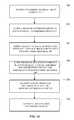
FIGS. 1 and 10 , in a first embodiment, a method of expelling gas betweensubstrate 12 andmold 52 is shown. More specifically, atstep 200, as mentioned above,polymeric material 100 may be positioned onsubstrate 12 by drop dispense, spin-coating, dip coating, chemical vapor deposition (CVD), physical vapor deposition (PVD), thin film deposition, thick film deposition, and the like. In a further embodiment,polymeric material 100 may be positioned onmold 52. - Referring to
FIGS. 6, 7 ,10, and11, atstep 202, a shape ofpatterning device 48 may be altered. More specifically, a shape ofpatterning device 48 may be altered such that a distance d1defined betweenmold 52 andsubstrate 12 at middle radius r3ofsubstrate 12, shown inFIG. 2 , is less than a distance defined betweenmold 52 andsubstrate 12 at remaining portions ofmold 52. In an example, distance d1is less than a distance d2, distance d2being defined at an edge ofmold 52. In a further embodiment, the distance d1may be defined at any desired location ofmold 52. The shape ofpatterning device 48 may be altered by controlling a pressure within first andthird chambers pump system 84 operates to control the pressure in first andthird chambers pump system 84 may create a vacuum within first andthird chambers throughway 80 such thatportions template 50 may bow away fromsubstrate 12 and bow towardstemplate chuck 60. As a result of bowingportions template 50 away fromsubstrate 12,portion 86boftemplate 50 bows towardsubstrate 12 and away fromtemplate chuck 60. - Referring to
FIGS. 10, 12 , and13, atstep 204, as described above with respect toFIG. 1 , eitherimprint head 97, shown inFIG. 1 ,stage 16, or both, may vary distance d1, shown inFIG. 11 , such that a portion ofmold 52 contacts a sub-portion ofdroplets 102. As shown, a portion ofmold 52 in superimposition with middle radius r3ofsubstrate 12, shown inFIG. 2 , contacts a sub-portion ofdroplets 102 prior to the remaining portions ofmold 52 contacting the remaining droplets ofdroplets 102. However, in a further embodiment, any portion ofmold 52 may contactdroplets 102 prior to remaining portions ofmold 52. To that end, as shown,mold 52 contacts all ofdroplets 102 in superimposition with middle radius r3ofsubstrate 12, shown inFIG. 2 , substantially concurrently. This causesdroplets 102 to spread and to produce acontiguous liquid sheet 130 ofpolymeric material 100.Edge 132 ofliquid sheet 130 defines a liquid-gas interface 134 that functions to push gases involume 128 towardedge 136 ofsubstrate 12.Volume 128 betweendroplets 102 define gas passages through which gas may be pushed to edge136. As a result, liquid-gas interface 134 in conjunction with the gas passages reduces, if not prevents, trapping of gases inliquid sheet 130. - Referring to
FIGS. 7, 10 , and14, atstep 206, the shape ofpatterning device 48 may be altered such that the desired volume defined betweenmold 52 andsubstrate 12 may be filled bypolymeric material 100, as described above with respect toFIG. 1 . More specifically, the shape ofpatterning device 48 may be altered by the combination of controlling the pressure within first andthird chambers 88 and96 and a force exerted byimprint head 97, shown inFIG. 1 , and/orstage 16 uponpatterning device 48 as a result of contact beenpolymeric material 100 andmold 52. More specifically, as mentioned above,pump system 84 operates to control the pressure in first andthird chambers 88 and96. To that end,pump system 84 decreases a magnitude of the vacuum created within first andthird chambers 88 and96 viathroughway 80 such thatpolymeric material 100 associated with subsequent subsets ofdroplets 100 surrounding middle radius r3ofsubstrate 12 shown inFIG. 2 , spread to become included incontiguous fluid sheet 130, as shown inFIG. 14 . The shape ofpatterning device 48 continues to be altered such thatmold 52 subsequently comes into contact with the remainingdroplets 102 so thatpolymeric material 100 associated therewith spreads to become included incontiguous sheet 130, as shown inFIG. 15 . As can be seen,interface 134 has moved towardsedge 136 so that there is an unimpeded path for the gases in the remainingvolume 128, shown inFIG. 8 , to travel thereto. This allows gases involume 128, shown inFIG. 8 , to egress from betweenmold 52 andsubstrate 12 vis-à-visedge 136. In this manner, the trapping of gas and/or gas pockets betweensubstrate 12 andmold 52 and within patternedlayer 114, shown inFIG. 9 , is minimized, if not prevented. In a further embodiment, the shape ofpatterning device 48 may be altered concurrently with decreasing the distance d1, as mentioned above with respect toFIG. 11 . - Referring to
FIGS. 7 and 12 , in still a further embodiment, to facilitate altering a shape ofpatterning device 48, a pressure withinsecond chamber 92 may be controlled. More specifically, as mentioned above,pump system 84 operates to control the pressure insecond chamber 92. To that end,pump system 84 may create a pressure withinsecond chamber 92 viathroughway 82 such thatportion 86coftemplate 50 may bow towardssubstrate 12 and bow away fromtemplate chuck 60. Further, a pressure may be created withinsecond chamber 92 concurrently with creating a vacuum in first andthird chamber 88 and96, as mentioned above. - Referring to
FIGS. 1 and 10 , atstep 208, as mentioned above with respect toFIG. 1 ,polymeric material 100 may be then be solidified and/or cross-linked, defining patternedlayer 114, shown inFIG. 9 . Subsequently, atstep 210,mold 52 may be separated from patternedlayer 114, shown inFIG. 9 . - Referring to
FIGS. 1 and 16 , a further embodiment of the present invention is shown. More specifically, atstep 300, analogous to that mentioned above with respect to step200, shown inFIG. 10 ,polymeric material 100 may be positioned onsubstrate 12 ormold 52. - Referring to
FIGS. 3, 4 ,16, and17, atstep 302, analogous to that mentioned above with respect to step202, shown inFIG. 10 , a shape ofpatterning device 48 may be altered. Furthermore, concurrently with altering a shape ofpatterning device 48, a shape ofsubstrate 12 may be altered. More specifically, a shape ofsubstrate 12 may be altered by controlling a pressure within first andthird chambers pump system 38 operates to control the pressure in first andthird chambers pump system 38 may create a vacuum within first andthird chambers throughway 36 such thatportions substrate 12 may bow away fromsubstrate chuck 14 and bow towardsmold 52, as shown inFIG. 17 . As a result of bowingportions substrate 12 toward fromsubstrate chuck 14,portion 40bofsubstrate 12 bows towardmold 52 and away fromsubstrate chuck 14. Referring toFIGS. 11, 13 , and16, atstep 304, analaogus to that mentioned above with respect to step204, shown inFIG. 10 ,imprint head 97,stage 16, or both, may vary distance d1, shown inFIG. 11 , such that a portion ofmold 52 contacts a sub-portion ofdroplets 102 in superimposition with middle radius r3ofsubstrate 12, shown inFIG. 2 , substantially concurrently, producingcontiguous liquid sheet 130 ofpolymeric material 100. - Referring to
FIGS. 4, 12 , and16, atstep 306, analogous to that mentioned above with respect to step206, shown inFIG. 10 , the shape ofpatterning device 48 may be altered such that the desired volume defined betweenmold 52 andsubstrate 12 may be filled bypolymeric material 100. Furthermore, concurrently with altering the shape ofpatterning device 48, the shape ofsubstrate 12 may be altered. More specifically, as mentioned above,pump system 38 operates to control the pressure in first andthird chambers pump system 38 decreases a magnitude of the vacuum created within first andthird chambers throughway 36 concurrently with altering a shape ofpatterning device 48 as mentioned above instep 204, shown inFIG. 10 , such thatpolymeric material 100 associated withdroplets 102 surrounding middle radius r3ofsubstrate 12, shown inFIG. 2 , spread to become included incontiguous fluid sheet 130, as shown inFIG. 14 . The shape ofsubstrate 12 may be further altered concurrently with the shape ofpatterning device 48 being altered such thatmold 52 subsequently comes into contact with the remainingdroplets 102 so thatpolymeric material 100 associated therewith spreads to become included incontiguous sheet 130, as shown inFIG. 15 . The gases involume 128, shown inFIG. 8 may egress from betweenmold 52 andsubstrate 12 vis-à-visedge 136 in substantially the same method as mentioned above with respect to step206, shown inFIG. 10 . - Referring to
FIGS. 3 and 4 , to further facilitate altering a shape ofsubstrate 12, a pressure withinsecond chamber 44 may be controlled. More specifically, as mentioned above,pump system 38 operates to control the pressure insecond chamber 44. To that end,pump system 38 may create a pressure withinsecond chamber 44 viathroughway 34 such thatportion 40boftemplate 50 may bow towardsmold 52 and bow away fromsubstrate chuck 14. Further, a pressure may be created withinsecond chamber 44 concurrently with creating a vacuum in first andthird chamber - Referring to
FIGS. 1 and 10 , atstep 308, as mentioned above with respect toFIG. 1 ,polymeric material 100 may be then be solidified and/or cross-linked, defining patternedlayer 114, shown inFIG. 9 . Subsequently, atstep 310,mold 52 may be separated from patternedlayer 114, shown inFIG. 9 . - Referring to
FIGS. 6 and 18 , in a further embodiment, to facilitate altering a shape ofpatterning device 48,pin 126 may be employed. More specifically, pin126 may exert a force upon patterningdevice 48, and in the present example, uponthird portion 86coftemplate 50. As a result,patterning device 48 may comprise the aforementioned desired altered shape and may be employed in any of the methods mentioned above.Pin 126 may be also employed to facilitate separation ofmold 52 andsubstrate 12, as mentioned above with respect tosteps FIGS. 10 and 16 , respectively. Furthermore, after formation of patternedlayer 114, shown inFIG. 9 , pin126 may translate away frompatterned device 48 such thatpatterning device 48 may be substantially flat.Pin 126 may be in communication withprocessor 122 such thatpin 126 may employ force feedback to determine a magnitude of the force. - Referring to
FIG. 19 , to further facilitate separation ofmold 52 andsubstrate 12, agas 148 may be introduced betweensubstrate 12 andmold 52 viapin 126. More specifically, pin126 may comprise athroughway 150 havingapertures 152 in fluid communication with a pressure control system, such as apump system 38. In a further embodiment, pin126 may comprise any number of apertures.Apertures 152 may be positioned to introducegas 148 betweenmold 52 andsubstrate 12.Gas 148 exerts a force uponmold 52 andsubstrate 12 to pushmold 52 in a direction away fromsubstrate 12 and to pushsubstrate 12 in a direction away frommold 52. As shown,gas 148 may be introduced betweenmold 52 andsubstrate 12 whenpin 126 is proximate totemplate 50; however, in a further embodiment,gas 148 may be introduced betweenmold 52 andsubstrate 12 whenpin 126 is in any position. - The embodiments of the present invention described above are exemplary. Many changes and modifications may be made to the disclosure recited above, while remaining within the scope of the invention. Therefore, the scope of the invention should not be limited by the above description, but instead should be determined with reference to the appended claims along with their full scope of equivalents.
Claims (20)
Priority Applications (2)
| Application Number | Priority Date | Filing Date | Title |
|---|---|---|---|
| US11/749,909US7641840B2 (en) | 2002-11-13 | 2007-05-17 | Method for expelling gas positioned between a substrate and a mold |
| US12/582,091US8215946B2 (en) | 2006-05-18 | 2009-10-20 | Imprint lithography system and method |
Applications Claiming Priority (7)
| Application Number | Priority Date | Filing Date | Title |
|---|---|---|---|
| US10/293,224US7019819B2 (en) | 2002-11-13 | 2002-11-13 | Chucking system for modulating shapes of substrates |
| US74838005P | 2005-12-08 | 2005-12-08 | |
| US11/389,731US7224443B2 (en) | 2002-11-13 | 2006-03-27 | Imprint lithography substrate processing tool for modulating shapes of substrates |
| US80126506P | 2006-05-18 | 2006-05-18 | |
| US82712806P | 2006-09-27 | 2006-09-27 | |
| US11/565,393US7691313B2 (en) | 2002-11-13 | 2006-11-30 | Method for expelling gas positioned between a substrate and a mold |
| US11/749,909US7641840B2 (en) | 2002-11-13 | 2007-05-17 | Method for expelling gas positioned between a substrate and a mold |
Related Parent Applications (2)
| Application Number | Title | Priority Date | Filing Date |
|---|---|---|---|
| US11/389,731ContinuationUS7224443B2 (en) | 2002-07-11 | 2006-03-27 | Imprint lithography substrate processing tool for modulating shapes of substrates |
| US11/565,393Continuation-In-PartUS7691313B2 (en) | 2002-07-11 | 2006-11-30 | Method for expelling gas positioned between a substrate and a mold |
Related Child Applications (1)
| Application Number | Title | Priority Date | Filing Date |
|---|---|---|---|
| US12/582,091Continuation-In-PartUS8215946B2 (en) | 2006-05-18 | 2009-10-20 | Imprint lithography system and method |
Publications (2)
| Publication Number | Publication Date |
|---|---|
| US20070228589A1true US20070228589A1 (en) | 2007-10-04 |
| US7641840B2 US7641840B2 (en) | 2010-01-05 |
Family
ID=38557622
Family Applications (1)
| Application Number | Title | Priority Date | Filing Date |
|---|---|---|---|
| US11/749,909Expired - LifetimeUS7641840B2 (en) | 2002-11-13 | 2007-05-17 | Method for expelling gas positioned between a substrate and a mold |
Country Status (1)
| Country | Link |
|---|---|
| US (1) | US7641840B2 (en) |
Cited By (32)
| Publication number | Priority date | Publication date | Assignee | Title |
|---|---|---|---|---|
| US20070231422A1 (en)* | 2006-04-03 | 2007-10-04 | Molecular Imprints, Inc. | System to vary dimensions of a thin template |
| US20080160129A1 (en)* | 2006-05-11 | 2008-07-03 | Molecular Imprints, Inc. | Template Having a Varying Thickness to Facilitate Expelling a Gas Positioned Between a Substrate and the Template |
| US20080174046A1 (en)* | 2002-07-11 | 2008-07-24 | Molecular Imprints Inc. | Capillary Imprinting Technique |
| US20090243153A1 (en)* | 2008-04-01 | 2009-10-01 | Molecular Imprints, Inc. | Large Area Roll-To-Roll Imprint Lithography |
| US7635263B2 (en) | 2005-01-31 | 2009-12-22 | Molecular Imprints, Inc. | Chucking system comprising an array of fluid chambers |
| US7636999B2 (en) | 2005-01-31 | 2009-12-29 | Molecular Imprints, Inc. | Method of retaining a substrate to a wafer chuck |
| US20100007868A1 (en)* | 2004-05-28 | 2010-01-14 | Board Of Regents, The University Of Texas System | Substrate Support System Having a Plurality of Contact Lands |
| US7670530B2 (en) | 2006-01-20 | 2010-03-02 | Molecular Imprints, Inc. | Patterning substrates employing multiple chucks |
| US7670529B2 (en) | 2005-12-08 | 2010-03-02 | Molecular Imprints, Inc. | Method and system for double-sided patterning of substrates |
| US20100059904A1 (en)* | 2008-09-11 | 2010-03-11 | Canon Kabushiki Kaisha | Imprint apparatus |
| US7691313B2 (en) | 2002-11-13 | 2010-04-06 | Molecular Imprints, Inc. | Method for expelling gas positioned between a substrate and a mold |
| US20100193994A1 (en)* | 2009-02-04 | 2010-08-05 | Asml Netherlands B.V. | Imprint lithography method and apparatus |
| US20100255139A1 (en)* | 2009-04-03 | 2010-10-07 | Ryuta Washiya | Micropattern transfer stamper and micropattern transfer device |
| US20100273027A1 (en)* | 2009-04-23 | 2010-10-28 | Samsung Electronics Co., Ltd. | Magnetic printing stamp, method of manufacturing magnetic printing stamp and magnetic printing method |
| US20100314803A1 (en)* | 2005-01-31 | 2010-12-16 | Molecular Imprints, Inc. | Chucking System for Nano-Manufacturing |
| US20100320645A1 (en)* | 2009-06-19 | 2010-12-23 | Molecular Imprints, Inc. | Dual zone template chuck |
| US20110180965A1 (en)* | 2010-01-22 | 2011-07-28 | Nanonex Corporation | Fast nanoimprinting apparatus using deformale mold |
| US20110272838A1 (en)* | 2010-05-06 | 2011-11-10 | Matt Malloy | Apparatus, System, and Method for Nanoimprint Template with a Backside Recess Having Tapered Sidewalls |
| US20120015065A1 (en)* | 2009-03-26 | 2012-01-19 | Marel Townsend Further Processing B.V. | Mass-distributing device and moulding device comprising a mass-distributing device of this type |
| US20120306122A1 (en)* | 2010-02-16 | 2012-12-06 | Tokyo Electron Limited | Imprinting method |
| CN101853801B (en)* | 2009-03-31 | 2013-04-24 | 台湾积体电路制造股份有限公司 | Method and apparatus of holding a device |
| US20140141135A1 (en)* | 2011-05-24 | 2014-05-22 | Hendrikus Cornelis Koos van Doom | Moulding device and method for moulding a food product |
| US20140191441A1 (en)* | 2011-09-21 | 2014-07-10 | Canon Kabushiki Kaisha | Imprint apparatus and article manufacturing method using same |
| US20140199426A1 (en)* | 2010-06-07 | 2014-07-17 | Lg Display Co., Ltd. | Imprinting apparatus and imprinting method using the same |
| US20170291350A1 (en)* | 2016-04-12 | 2017-10-12 | Iai Industrial Systems B.V. | Method and apparatus for applying a layer having a relief on a flat face of a substrate |
| KR20180071971A (en)* | 2016-12-20 | 2018-06-28 | 캐논 가부시끼가이샤 | Methods for controlling extrusions during imprint template replication processes |
| KR20180090357A (en)* | 2015-12-16 | 2018-08-10 | 캐논 가부시끼가이샤 | Imprint apparatus and article manufacturing method |
| US10108086B2 (en) | 2013-03-15 | 2018-10-23 | Nanonex Corporation | System and methods of mold/substrate separation for imprint lithography |
| US10105883B2 (en) | 2013-03-15 | 2018-10-23 | Nanonex Corporation | Imprint lithography system and method for manufacturing |
| TWI708307B (en)* | 2011-08-12 | 2020-10-21 | Ev集團E塔那有限公司 | Device and method for bonding of substrates |
| EP3950148A1 (en)* | 2013-08-19 | 2022-02-09 | Board Of Regents Of the University Of Texas System | Programmable deposition of thin films of a user-defined profile with nanometer scale accuracy |
| WO2023141583A3 (en)* | 2022-01-20 | 2023-09-07 | Magic Leap, Inc. | Surface relief waveguides with high refractive index resist |
Families Citing this family (10)
| Publication number | Priority date | Publication date | Assignee | Title |
|---|---|---|---|---|
| US20070228608A1 (en)* | 2006-04-03 | 2007-10-04 | Molecular Imprints, Inc. | Preserving Filled Features when Vacuum Wiping |
| US8215946B2 (en) | 2006-05-18 | 2012-07-10 | Molecular Imprints, Inc. | Imprint lithography system and method |
| CN101808808B (en) | 2007-09-28 | 2013-05-01 | 东丽株式会社 | Method and device for manufacturing sheet having fine shape transferred thereon |
| US20100096764A1 (en)* | 2008-10-20 | 2010-04-22 | Molecular Imprints, Inc. | Gas Environment for Imprint Lithography |
| US8652393B2 (en) | 2008-10-24 | 2014-02-18 | Molecular Imprints, Inc. | Strain and kinetics control during separation phase of imprint process |
| US8309008B2 (en)* | 2008-10-30 | 2012-11-13 | Molecular Imprints, Inc. | Separation in an imprint lithography process |
| WO2010111307A1 (en)* | 2009-03-23 | 2010-09-30 | Intevac, Inc. | A process for optimization of island to trench ratio in patterned media |
| JP5875250B2 (en)* | 2011-04-28 | 2016-03-02 | キヤノン株式会社 | Imprint apparatus, imprint method, and device manufacturing method |
| TWI672212B (en)* | 2016-08-25 | 2019-09-21 | 國立成功大學 | Nano imprinting assembly and imprinting method thereof |
| JP7256773B2 (en)* | 2020-04-24 | 2023-04-12 | 信越化学工業株式会社 | Flatness control method, coating film forming method, flatness control apparatus, and coating film forming apparatus |
Citations (90)
| Publication number | Priority date | Publication date | Assignee | Title |
|---|---|---|---|---|
| US3637381A (en)* | 1966-09-22 | 1972-01-25 | Teeg Research Inc | Radiation-sensitive self-revealing elements and methods of making and utilizing the same |
| US4148549A (en)* | 1975-12-08 | 1979-04-10 | The Rank Organisation Ltd. | Diffraction gratings |
| US4279628A (en)* | 1979-12-31 | 1981-07-21 | Energy Synergistics, Inc. | Apparatus for drying a natural gas stream |
| US4312823A (en)* | 1977-03-14 | 1982-01-26 | U.S. Philips Corporation | Method of manufacturing a plastic record carrier having a stratified structure |
| US4395211A (en)* | 1979-08-10 | 1983-07-26 | U.S. Philips Corporation | Method and device for manufacturing a plastic record carrier |
| US4506184A (en)* | 1984-01-10 | 1985-03-19 | Varian Associates, Inc. | Deformable chuck driven by piezoelectric means |
| US4512848A (en)* | 1984-02-06 | 1985-04-23 | Exxon Research And Engineering Co. | Procedure for fabrication of microstructures over large areas using physical replication |
| US4521175A (en)* | 1980-03-14 | 1985-06-04 | Multivac Sepp Haggenmuller Kg | Apparatus for producing containers from thermoplastic sheet material |
| US4689004A (en)* | 1985-04-18 | 1987-08-25 | Firma Carl Freudenberg | Apparatus for adhering thermally-softenable plastic particles into a plastic body |
| US4724222A (en)* | 1986-04-28 | 1988-02-09 | American Telephone And Telegraph Company, At&T Bell Laboratories | Wafer chuck comprising a curved reference surface |
| US4731155A (en)* | 1987-04-15 | 1988-03-15 | General Electric Company | Process for forming a lithographic mask |
| US4767584A (en)* | 1985-04-03 | 1988-08-30 | Massachusetts Institute Of Technology | Process of and apparatus for producing design patterns in materials |
| US5028361A (en)* | 1987-11-09 | 1991-07-02 | Takeo Fujimoto | Method for molding a photosensitive composition |
| US5028366A (en)* | 1988-01-12 | 1991-07-02 | Air Products And Chemicals, Inc. | Water based mold release compositions for making molded polyurethane foam |
| US5213600A (en)* | 1987-06-09 | 1993-05-25 | International Business Machines Corp. | Method of manufacturing an optical storage disk |
| US5324012A (en)* | 1991-07-16 | 1994-06-28 | Nikon Corporation | Holding apparatus for holding an article such as a semiconductor wafer |
| US5331371A (en)* | 1990-09-26 | 1994-07-19 | Canon Kabushiki Kaisha | Alignment and exposure method |
| US5338177A (en)* | 1992-04-22 | 1994-08-16 | Societe Nationale Industrielle Et Aerospatiale | Hot compacting device for the production of parts requiring simultaneous pressure and temperature rises |
| US5425848A (en)* | 1993-03-16 | 1995-06-20 | U.S. Philips Corporation | Method of providing a patterned relief of cured photoresist on a flat substrate surface and device for carrying out such a method |
| US5512131A (en)* | 1993-10-04 | 1996-04-30 | President And Fellows Of Harvard College | Formation of microstamped patterns on surfaces and derivative articles |
| US5515167A (en)* | 1994-09-13 | 1996-05-07 | Hughes Aircraft Company | Transparent optical chuck incorporating optical monitoring |
| US5527662A (en)* | 1990-05-24 | 1996-06-18 | Matsushita Electric Industrial Co., Ltd. | Process for forming fine pattern |
| US5534073A (en)* | 1992-09-07 | 1996-07-09 | Mitsubishi Denki Kabushiki Kaisha | Semiconductor producing apparatus comprising wafer vacuum chucking device |
| US5545367A (en)* | 1992-04-15 | 1996-08-13 | Soane Technologies, Inc. | Rapid prototype three dimensional stereolithography |
| US5550654A (en)* | 1993-07-19 | 1996-08-27 | Lucent Technologies Inc. | Method for forming, in optical media, refractive index perturbations having reduced birefringence |
| US5601641A (en)* | 1992-07-21 | 1997-02-11 | Tse Industries, Inc. | Mold release composition with polybutadiene and method of coating a mold core |
| US5772905A (en)* | 1995-11-15 | 1998-06-30 | Regents Of The University Of Minnesota | Nanoimprint lithography |
| US5776748A (en)* | 1993-10-04 | 1998-07-07 | President And Fellows Of Harvard College | Method of formation of microstamped patterns on plates for adhesion of cells and other biological materials, devices and uses therefor |
| US5900062A (en)* | 1995-12-28 | 1999-05-04 | Applied Materials, Inc. | Lift pin for dechucking substrates |
| US5923408A (en)* | 1996-01-31 | 1999-07-13 | Canon Kabushiki Kaisha | Substrate holding system and exposure apparatus using the same |
| US6019166A (en)* | 1997-12-30 | 2000-02-01 | Intel Corporation | Pickup chuck with an integral heatsink |
| US6030275A (en)* | 1998-03-17 | 2000-02-29 | International Business Machines Corporation | Variable control of carrier curvature with direct feedback loop |
| US6032506A (en)* | 1996-05-30 | 2000-03-07 | S.C. Recherche Et Developpement Groupe | Improvment to the blank holder force regulating system in a press |
| US6099771A (en)* | 1998-07-08 | 2000-08-08 | Lear Corporation | Vacuum compression method for forming molded thermoplastic floor mat having a "Class A" finish |
| US6182510B1 (en)* | 1997-04-30 | 2001-02-06 | Sensys Instruments Corporation | Apparatus and method for characterizing semiconductor wafers during processing |
| US6218316B1 (en)* | 1998-10-22 | 2001-04-17 | Micron Technology, Inc. | Planarization of non-planar surfaces in device fabrication |
| US6220561B1 (en)* | 1999-06-30 | 2001-04-24 | Sandia Corporation | Compound floating pivot micromechanisms |
| US6247579B1 (en)* | 1999-01-18 | 2001-06-19 | Tokyo Ohka Kogyo Co., Ltd | Substrate transfer apparatus and method of substrate transfer |
| US6257866B1 (en)* | 1996-06-18 | 2001-07-10 | Hy-Tech Forming Systems, Inc. | Apparatus for accurately forming plastic sheet |
| US6334960B1 (en)* | 1999-03-11 | 2002-01-01 | Board Of Regents, The University Of Texas System | Step and flash imprint lithography |
| US6355198B1 (en)* | 1996-03-15 | 2002-03-12 | President And Fellows Of Harvard College | Method of forming articles including waveguides via capillary micromolding and microtransfer molding |
| US20020042027A1 (en)* | 1998-10-09 | 2002-04-11 | Chou Stephen Y. | Microscale patterning and articles formed thereby |
| US6383890B2 (en)* | 1997-12-26 | 2002-05-07 | Canon Kabushiki Kaisha | Wafer bonding method, apparatus and vacuum chuck |
| US6391217B2 (en)* | 1999-12-23 | 2002-05-21 | University Of Massachusetts | Methods and apparatus for forming submicron patterns on films |
| US6407006B1 (en)* | 1999-09-09 | 2002-06-18 | Honeywell International, Inc. | Method for integrated circuit planarization |
| US6416311B1 (en)* | 1998-05-04 | 2002-07-09 | Jenoptik Aktiengesellschaft | Device and method for separating a shaped substrate from a stamping tool |
| US20020094496A1 (en)* | 2000-07-17 | 2002-07-18 | Choi Byung J. | Method and system of automatic fluid dispensing for imprint lithography processes |
| US6512401B2 (en)* | 1999-09-10 | 2003-01-28 | Intel Corporation | Output buffer for high and low voltage bus |
| US6517995B1 (en)* | 1999-09-14 | 2003-02-11 | Massachusetts Institute Of Technology | Fabrication of finely featured devices by liquid embossing |
| US6518189B1 (en)* | 1995-11-15 | 2003-02-11 | Regents Of The University Of Minnesota | Method and apparatus for high density nanostructures |
| US20030034329A1 (en)* | 1998-06-30 | 2003-02-20 | Chou Stephen Y. | Lithographic method for molding pattern with nanoscale depth |
| US20030062334A1 (en)* | 2001-09-25 | 2003-04-03 | Lee Hong Hie | Method for forming a micro-pattern on a substrate by using capillary force |
| US20030080471A1 (en)* | 2001-10-29 | 2003-05-01 | Chou Stephen Y. | Lithographic method for molding pattern with nanoscale features |
| US6580172B2 (en)* | 2001-03-02 | 2003-06-17 | Motorola, Inc. | Lithographic template and method of formation and use |
| US20040009673A1 (en)* | 2002-07-11 | 2004-01-15 | Sreenivasan Sidlgata V. | Method and system for imprint lithography using an electric field |
| US20040022888A1 (en)* | 2002-08-01 | 2004-02-05 | Sreenivasan Sidlgata V. | Alignment systems for imprint lithography |
| US20040029041A1 (en)* | 2002-02-27 | 2004-02-12 | Brewer Science, Inc. | Novel planarization method for multi-layer lithography processing |
| US6696220B2 (en)* | 2000-10-12 | 2004-02-24 | Board Of Regents, The University Of Texas System | Template for room temperature, low pressure micro-and nano-imprint lithography |
| US20040036201A1 (en)* | 2000-07-18 | 2004-02-26 | Princeton University | Methods and apparatus of field-induced pressure imprint lithography |
| US20040046288A1 (en)* | 2000-07-18 | 2004-03-11 | Chou Stephen Y. | Laset assisted direct imprint lithography |
| US6726195B1 (en)* | 1998-10-13 | 2004-04-27 | Dek International Gmbh | Method for ensuring planarity when using a flexible, self conforming, workpiece support system |
| US6736408B2 (en)* | 2002-01-25 | 2004-05-18 | Applied Materials Inc. | Rotary vacuum-chuck with venturi formed at base of rotating shaft |
| US20040104641A1 (en)* | 1999-10-29 | 2004-06-03 | University Of Texas System | Method of separating a template from a substrate during imprint lithography |
| US20040110856A1 (en)* | 2002-12-04 | 2004-06-10 | Young Jung Gun | Polymer solution for nanoimprint lithography to reduce imprint temperature and pressure |
| US20040124566A1 (en)* | 2002-07-11 | 2004-07-01 | Sreenivasan Sidlgata V. | Step and repeat imprint lithography processes |
| US20040131718A1 (en)* | 2000-07-18 | 2004-07-08 | Princeton University | Lithographic apparatus for fluid pressure imprint lithography |
| US20040137734A1 (en)* | 1995-11-15 | 2004-07-15 | Princeton University | Compositions and processes for nanoimprinting |
| US6764368B2 (en)* | 1999-05-27 | 2004-07-20 | University Of North Carolina At Charlotte | Method of fabricating a cathodo-/electro-luminescent device using a porous silicon/porous silicon carbide as an electron emitter |
| US6771372B1 (en)* | 2001-11-01 | 2004-08-03 | Therma-Wave, Inc. | Rotational stage with vertical axis adjustment |
| US20040156108A1 (en)* | 2001-10-29 | 2004-08-12 | Chou Stephen Y. | Articles comprising nanoscale patterns with reduced edge roughness and methods of making same |
| US6776094B1 (en)* | 1993-10-04 | 2004-08-17 | President & Fellows Of Harvard College | Kit For Microcontact Printing |
| US6849558B2 (en)* | 2002-05-22 | 2005-02-01 | The Board Of Trustees Of The Leland Stanford Junior University | Replication and transfer of microstructures and nanostructures |
| US20050037143A1 (en)* | 2000-07-18 | 2005-02-17 | Chou Stephen Y. | Imprint lithography with improved monitoring and control and apparatus therefor |
| US6869980B2 (en)* | 2000-03-02 | 2005-03-22 | Celanese Ventures Gmbh | Polymer blend membranes for use in fuel cells |
| US6898064B1 (en)* | 2001-08-29 | 2005-05-24 | Lsi Logic Corporation | System and method for optimizing the electrostatic removal of a workpiece from a chuck |
| US6900881B2 (en)* | 2002-07-11 | 2005-05-31 | Molecular Imprints, Inc. | Step and repeat imprint lithography systems |
| US6916584B2 (en)* | 2002-08-01 | 2005-07-12 | Molecular Imprints, Inc. | Alignment methods for imprint lithography |
| US6932934B2 (en)* | 2002-07-11 | 2005-08-23 | Molecular Imprints, Inc. | Formation of discontinuous films during an imprint lithography process |
| US6982783B2 (en)* | 2002-11-13 | 2006-01-03 | Molecular Imprints, Inc. | Chucking system for modulating shapes of substrates |
| US7007992B2 (en)* | 2002-11-20 | 2006-03-07 | Young Freddie W | Internal tube gripping device |
| US7018572B2 (en)* | 2001-06-11 | 2006-03-28 | General Electric Company | Method for producing data storage media |
| US7023238B1 (en)* | 2004-01-07 | 2006-04-04 | Altera Corporation | Input buffer with selectable threshold and hysteresis option |
| US20060172553A1 (en)* | 2005-01-31 | 2006-08-03 | Molecular Imprints, Inc. | Method of retaining a substrate to a wafer chuck |
| US20060172549A1 (en)* | 2005-01-31 | 2006-08-03 | Molecular Imprints, Inc. | Method of separating a mold from a solidified layer disposed on a substrate |
| US7090716B2 (en)* | 2003-10-02 | 2006-08-15 | Molecular Imprints, Inc. | Single phase fluid imprint lithography method |
| US7179079B2 (en)* | 2002-07-08 | 2007-02-20 | Molecular Imprints, Inc. | Conforming template for patterning liquids disposed on substrates |
| US20070132152A1 (en)* | 2005-12-08 | 2007-06-14 | Molecular Imprints, Inc. | Method and System for Double-Sided Patterning of Substrates |
| US7245358B2 (en)* | 2004-05-28 | 2007-07-17 | Board Of Regents, The University Of Texas System | Substrate support system |
| US20070170617A1 (en)* | 2006-01-20 | 2007-07-26 | Molecular Imprints, Inc. | Patterning Substrates Employing Multiple Chucks |
| US20080174046A1 (en)* | 2002-07-11 | 2008-07-24 | Molecular Imprints Inc. | Capillary Imprinting Technique |
Family Cites Families (66)
| Publication number | Priority date | Publication date | Assignee | Title |
|---|---|---|---|---|
| US3997447A (en) | 1974-06-07 | 1976-12-14 | Composite Sciences, Inc. | Fluid processing apparatus |
| IT1068535B (en)* | 1975-11-03 | 1985-03-21 | Ibm | APPARATUS AND GRAPHIC ELECTROLYTE PROCESS |
| US4223261A (en) | 1978-08-23 | 1980-09-16 | Exxon Research & Engineering Co. | Multi-phase synchronous machine system |
| JPS5732629Y2 (en) | 1978-09-20 | 1982-07-17 | ||
| JPS57153434U (en) | 1981-03-20 | 1982-09-27 | ||
| JPS57204547A (en) | 1981-06-12 | 1982-12-15 | Hitachi Ltd | Exposing method |
| JPS5884808A (en) | 1981-11-13 | 1983-05-21 | Nippon Synthetic Chem Ind Co Ltd:The | Preparation of resinous material |
| US4551192A (en) | 1983-06-30 | 1985-11-05 | International Business Machines Corporation | Electrostatic or vacuum pinchuck formed with microcircuit lithography |
| JPS60127935U (en) | 1984-02-03 | 1985-08-28 | 三菱電機株式会社 | thermal head |
| US4559717A (en) | 1984-02-21 | 1985-12-24 | The United States Of America As Represented By The Secretary Of Commerce | Flexure hinge |
| EP0245461A1 (en) | 1985-11-18 | 1987-11-19 | EASTMAN KODAK COMPANY (a New Jersey corporation) | Process for making optical recording media |
| DE3639346A1 (en) | 1986-11-18 | 1988-05-26 | Siemens Ag | METHOD AND ARRANGEMENT FOR CHANGING THE IMAGE SCALE IN X-RAY LITHOGRAPHY |
| JPH01196749A (en) | 1988-01-30 | 1989-08-08 | Hoya Corp | Manufacture of substrate for optical information recording medium |
| US5821175A (en) | 1988-07-08 | 1998-10-13 | Cauldron Limited Partnership | Removal of surface contaminants by irradiation using various methods to achieve desired inert gas flow over treated surface |
| JPH0292603A (en) | 1988-09-30 | 1990-04-03 | Hoya Corp | Manufacture of data recording board with guide groove |
| JPH02192045A (en) | 1989-01-20 | 1990-07-27 | Fujitsu Ltd | Production of optical disk substrate |
| JPH0580530A (en) | 1991-09-24 | 1993-04-02 | Hitachi Ltd | Production of thin film pattern |
| JP2867194B2 (en)* | 1992-02-05 | 1999-03-08 | 東京エレクトロン株式会社 | Processing device and processing method |
| JPH08130207A (en) | 1994-10-31 | 1996-05-21 | Matsushita Electric Ind Co Ltd | Plasma processing device |
| US5563684A (en) | 1994-11-30 | 1996-10-08 | Sgs-Thomson Microelectronics, Inc. | Adaptive wafer modulator for placing a selected pattern on a semiconductor wafer |
| US5849209A (en) | 1995-03-31 | 1998-12-15 | Johnson & Johnson Vision Products, Inc. | Mold material made with additives |
| US5820769A (en) | 1995-05-24 | 1998-10-13 | Regents Of The University Of Minnesota | Method for making magnetic storage having discrete elements with quantized magnetic moments |
| US5997273A (en) | 1995-08-01 | 1999-12-07 | Laquer; Henry Louis | Differential pressure HIP forging in a controlled gaseous environment |
| US5849222A (en) | 1995-09-29 | 1998-12-15 | Johnson & Johnson Vision Products, Inc. | Method for reducing lens hole defects in production of contact lens blanks |
| US6482742B1 (en) | 2000-07-18 | 2002-11-19 | Stephen Y. Chou | Fluid pressure imprint lithography |
| US5669303A (en)* | 1996-03-04 | 1997-09-23 | Motorola | Apparatus and method for stamping a surface |
| US20030179354A1 (en) | 1996-03-22 | 2003-09-25 | Nikon Corporation | Mask-holding apparatus for a light exposure apparatus and related scanning-exposure method |
| JPH10172897A (en) | 1996-12-05 | 1998-06-26 | Nikon Corp | Substrate adapter, substrate holding device and substrate holding method |
| US5948470A (en) | 1997-04-28 | 1999-09-07 | Harrison; Christopher | Method of nanoscale patterning and products made thereby |
| AU3818997A (en) | 1997-07-25 | 1999-02-16 | Regents Of The University Of Minnesota | Single-electron floating-gate mos memory |
| EP0921683B1 (en) | 1997-12-02 | 2010-09-08 | Daewoo Electronics Corporation | Method and apparatus for encoding mode signals for use in a binary shape coder |
| US6304424B1 (en) | 1998-04-03 | 2001-10-16 | Applied Materials Inc. | Method and apparatus for minimizing plasma destabilization within a semiconductor wafer processing system |
| US5997963A (en) | 1998-05-05 | 1999-12-07 | Ultratech Stepper, Inc. | Microchamber |
| JP3780700B2 (en) | 1998-05-26 | 2006-05-31 | セイコーエプソン株式会社 | Pattern forming method, pattern forming apparatus, pattern forming plate, pattern forming plate manufacturing method, color filter manufacturing method, conductive film manufacturing method, and liquid crystal panel manufacturing method |
| US5947027A (en)* | 1998-09-08 | 1999-09-07 | Motorola, Inc. | Printing apparatus with inflatable means for advancing a substrate towards the stamping surface |
| US6965506B2 (en) | 1998-09-30 | 2005-11-15 | Lam Research Corporation | System and method for dechucking a workpiece from an electrostatic chuck |
| WO2000021689A1 (en) | 1998-10-09 | 2000-04-20 | The Trustees Of Princeton University | Microscale patterning and articles formed thereby |
| US6160430A (en) | 1999-03-22 | 2000-12-12 | Ati International Srl | Powerup sequence artificial voltage supply circuit |
| US6305677B1 (en) | 1999-03-30 | 2001-10-23 | Lam Research Corporation | Perimeter wafer lifting |
| JP3291488B2 (en) | 1999-05-27 | 2002-06-10 | 三洋電機株式会社 | Fluid removal method |
| EP1077393A2 (en)* | 1999-08-19 | 2001-02-21 | Canon Kabushiki Kaisha | Substrate attracting and holding system for use in exposure apparatus |
| US6313567B1 (en) | 2000-04-10 | 2001-11-06 | Motorola, Inc. | Lithography chuck having piezoelectric elements, and method |
| JP2001358056A (en) | 2000-06-15 | 2001-12-26 | Canon Inc | Exposure equipment |
| JP2004505273A (en)* | 2000-08-01 | 2004-02-19 | ボード・オブ・リージエンツ,ザ・ユニバーシテイ・オブ・テキサス・システム | Method for highly accurate sensing of gap and orientation between transparent template and substrate for transfer lithography |
| AU2001286573A1 (en) | 2000-08-21 | 2002-03-04 | Board Of Regents, The University Of Texas System | Flexure based macro motion translation stage |
| US6718630B2 (en) | 2000-09-18 | 2004-04-13 | Matsushita Electric Industrial Co., Ltd. | Apparatus and method for mounting components on substrate |
| WO2002047139A2 (en) | 2000-12-04 | 2002-06-13 | Ebara Corporation | Methode of forming a copper film on a substrate |
| US6612590B2 (en) | 2001-01-12 | 2003-09-02 | Tokyo Electron Limited | Apparatus and methods for manipulating semiconductor wafers |
| SG169225A1 (en) | 2001-07-25 | 2011-03-30 | Univ Princeton | Nanochannel arrays and their preparation and use for high throughput macromolecular analysis |
| US6764386B2 (en) | 2002-01-11 | 2004-07-20 | Applied Materials, Inc. | Air bearing-sealed micro-processing chamber |
| CA2380114C (en) | 2002-04-04 | 2010-01-19 | Obducat Aktiebolag | Imprint method and device |
| US20040132301A1 (en) | 2002-09-12 | 2004-07-08 | Harper Bruce M. | Indirect fluid pressure imprinting |
| US6980282B2 (en) | 2002-12-11 | 2005-12-27 | Molecular Imprints, Inc. | Method for modulating shapes of substrates |
| US6986815B2 (en) | 2003-01-08 | 2006-01-17 | General Electric Company | Flow system flush process |
| US6943117B2 (en) | 2003-03-27 | 2005-09-13 | Korea Institute Of Machinery & Materials | UV nanoimprint lithography process using elementwise embossed stamp and selectively additive pressurization |
| US6951173B1 (en) | 2003-05-14 | 2005-10-04 | Molecular Imprints, Inc. | Assembly and method for transferring imprint lithography templates |
| TWI228638B (en) | 2003-06-10 | 2005-03-01 | Ind Tech Res Inst | Method for and apparatus for bonding patterned imprint to a substrate by adhering means |
| US7150622B2 (en) | 2003-07-09 | 2006-12-19 | Molecular Imprints, Inc. | Systems for magnification and distortion correction for imprint lithography processes |
| WO2005018702A2 (en) | 2003-08-13 | 2005-03-03 | Medtronic, Inc. | Active agent delivery systems including a miscible polymer blend, medical devices, and methods |
| US6879191B2 (en) | 2003-08-26 | 2005-04-12 | Intel Corporation | Voltage mismatch tolerant input/output buffer |
| EP1594001B1 (en)* | 2004-05-07 | 2015-12-30 | Obducat AB | Device and method for imprint lithography |
| WO2005119802A2 (en) | 2004-05-28 | 2005-12-15 | Board Of Regents, The University Of Texas System | Adaptive shape substrate support system and method |
| US7768624B2 (en) | 2004-06-03 | 2010-08-03 | Board Of Regents, The University Of Texas System | Method for obtaining force combinations for template deformation using nullspace and methods optimization techniques |
| US7635263B2 (en) | 2005-01-31 | 2009-12-22 | Molecular Imprints, Inc. | Chucking system comprising an array of fluid chambers |
| US7316554B2 (en) | 2005-09-21 | 2008-01-08 | Molecular Imprints, Inc. | System to control an atmosphere between a body and a substrate |
| US20070231422A1 (en) | 2006-04-03 | 2007-10-04 | Molecular Imprints, Inc. | System to vary dimensions of a thin template |
- 2007
- 2007-05-17USUS11/749,909patent/US7641840B2/ennot_activeExpired - Lifetime
Patent Citations (99)
| Publication number | Priority date | Publication date | Assignee | Title |
|---|---|---|---|---|
| US3637381A (en)* | 1966-09-22 | 1972-01-25 | Teeg Research Inc | Radiation-sensitive self-revealing elements and methods of making and utilizing the same |
| US4148549A (en)* | 1975-12-08 | 1979-04-10 | The Rank Organisation Ltd. | Diffraction gratings |
| US4312823A (en)* | 1977-03-14 | 1982-01-26 | U.S. Philips Corporation | Method of manufacturing a plastic record carrier having a stratified structure |
| US4395211A (en)* | 1979-08-10 | 1983-07-26 | U.S. Philips Corporation | Method and device for manufacturing a plastic record carrier |
| US4279628A (en)* | 1979-12-31 | 1981-07-21 | Energy Synergistics, Inc. | Apparatus for drying a natural gas stream |
| US4521175A (en)* | 1980-03-14 | 1985-06-04 | Multivac Sepp Haggenmuller Kg | Apparatus for producing containers from thermoplastic sheet material |
| US4506184A (en)* | 1984-01-10 | 1985-03-19 | Varian Associates, Inc. | Deformable chuck driven by piezoelectric means |
| US4512848A (en)* | 1984-02-06 | 1985-04-23 | Exxon Research And Engineering Co. | Procedure for fabrication of microstructures over large areas using physical replication |
| US4767584A (en)* | 1985-04-03 | 1988-08-30 | Massachusetts Institute Of Technology | Process of and apparatus for producing design patterns in materials |
| US4689004A (en)* | 1985-04-18 | 1987-08-25 | Firma Carl Freudenberg | Apparatus for adhering thermally-softenable plastic particles into a plastic body |
| US4724222A (en)* | 1986-04-28 | 1988-02-09 | American Telephone And Telegraph Company, At&T Bell Laboratories | Wafer chuck comprising a curved reference surface |
| US4731155A (en)* | 1987-04-15 | 1988-03-15 | General Electric Company | Process for forming a lithographic mask |
| US5213600A (en)* | 1987-06-09 | 1993-05-25 | International Business Machines Corp. | Method of manufacturing an optical storage disk |
| US5427599A (en)* | 1987-06-09 | 1995-06-27 | International Business Machines Corporation | System for stamping an optical storage disk |
| US5028361A (en)* | 1987-11-09 | 1991-07-02 | Takeo Fujimoto | Method for molding a photosensitive composition |
| US5028366A (en)* | 1988-01-12 | 1991-07-02 | Air Products And Chemicals, Inc. | Water based mold release compositions for making molded polyurethane foam |
| US5527662A (en)* | 1990-05-24 | 1996-06-18 | Matsushita Electric Industrial Co., Ltd. | Process for forming fine pattern |
| US5331371A (en)* | 1990-09-26 | 1994-07-19 | Canon Kabushiki Kaisha | Alignment and exposure method |
| US5324012A (en)* | 1991-07-16 | 1994-06-28 | Nikon Corporation | Holding apparatus for holding an article such as a semiconductor wafer |
| US5545367A (en)* | 1992-04-15 | 1996-08-13 | Soane Technologies, Inc. | Rapid prototype three dimensional stereolithography |
| US5338177A (en)* | 1992-04-22 | 1994-08-16 | Societe Nationale Industrielle Et Aerospatiale | Hot compacting device for the production of parts requiring simultaneous pressure and temperature rises |
| US5601641A (en)* | 1992-07-21 | 1997-02-11 | Tse Industries, Inc. | Mold release composition with polybutadiene and method of coating a mold core |
| US5534073A (en)* | 1992-09-07 | 1996-07-09 | Mitsubishi Denki Kabushiki Kaisha | Semiconductor producing apparatus comprising wafer vacuum chucking device |
| US5425848A (en)* | 1993-03-16 | 1995-06-20 | U.S. Philips Corporation | Method of providing a patterned relief of cured photoresist on a flat substrate surface and device for carrying out such a method |
| US5550654A (en)* | 1993-07-19 | 1996-08-27 | Lucent Technologies Inc. | Method for forming, in optical media, refractive index perturbations having reduced birefringence |
| US5512131A (en)* | 1993-10-04 | 1996-04-30 | President And Fellows Of Harvard College | Formation of microstamped patterns on surfaces and derivative articles |
| US6776094B1 (en)* | 1993-10-04 | 2004-08-17 | President & Fellows Of Harvard College | Kit For Microcontact Printing |
| US5776748A (en)* | 1993-10-04 | 1998-07-07 | President And Fellows Of Harvard College | Method of formation of microstamped patterns on plates for adhesion of cells and other biological materials, devices and uses therefor |
| US5515167A (en)* | 1994-09-13 | 1996-05-07 | Hughes Aircraft Company | Transparent optical chuck incorporating optical monitoring |
| US6518189B1 (en)* | 1995-11-15 | 2003-02-11 | Regents Of The University Of Minnesota | Method and apparatus for high density nanostructures |
| US20040137734A1 (en)* | 1995-11-15 | 2004-07-15 | Princeton University | Compositions and processes for nanoimprinting |
| US5772905A (en)* | 1995-11-15 | 1998-06-30 | Regents Of The University Of Minnesota | Nanoimprint lithography |
| US5900062A (en)* | 1995-12-28 | 1999-05-04 | Applied Materials, Inc. | Lift pin for dechucking substrates |
| US5923408A (en)* | 1996-01-31 | 1999-07-13 | Canon Kabushiki Kaisha | Substrate holding system and exposure apparatus using the same |
| US6355198B1 (en)* | 1996-03-15 | 2002-03-12 | President And Fellows Of Harvard College | Method of forming articles including waveguides via capillary micromolding and microtransfer molding |
| US6032506A (en)* | 1996-05-30 | 2000-03-07 | S.C. Recherche Et Developpement Groupe | Improvment to the blank holder force regulating system in a press |
| US6257866B1 (en)* | 1996-06-18 | 2001-07-10 | Hy-Tech Forming Systems, Inc. | Apparatus for accurately forming plastic sheet |
| US6182510B1 (en)* | 1997-04-30 | 2001-02-06 | Sensys Instruments Corporation | Apparatus and method for characterizing semiconductor wafers during processing |
| US6383890B2 (en)* | 1997-12-26 | 2002-05-07 | Canon Kabushiki Kaisha | Wafer bonding method, apparatus and vacuum chuck |
| US6019166A (en)* | 1997-12-30 | 2000-02-01 | Intel Corporation | Pickup chuck with an integral heatsink |
| US6030275A (en)* | 1998-03-17 | 2000-02-29 | International Business Machines Corporation | Variable control of carrier curvature with direct feedback loop |
| US6416311B1 (en)* | 1998-05-04 | 2002-07-09 | Jenoptik Aktiengesellschaft | Device and method for separating a shaped substrate from a stamping tool |
| US20030034329A1 (en)* | 1998-06-30 | 2003-02-20 | Chou Stephen Y. | Lithographic method for molding pattern with nanoscale depth |
| US6099771A (en)* | 1998-07-08 | 2000-08-08 | Lear Corporation | Vacuum compression method for forming molded thermoplastic floor mat having a "Class A" finish |
| US20020042027A1 (en)* | 1998-10-09 | 2002-04-11 | Chou Stephen Y. | Microscale patterning and articles formed thereby |
| US20040118809A1 (en)* | 1998-10-09 | 2004-06-24 | Chou Stephen Y. | Microscale patterning and articles formed thereby |
| US6713238B1 (en)* | 1998-10-09 | 2004-03-30 | Stephen Y. Chou | Microscale patterning and articles formed thereby |
| US6726195B1 (en)* | 1998-10-13 | 2004-04-27 | Dek International Gmbh | Method for ensuring planarity when using a flexible, self conforming, workpiece support system |
| US6218316B1 (en)* | 1998-10-22 | 2001-04-17 | Micron Technology, Inc. | Planarization of non-planar surfaces in device fabrication |
| US6247579B1 (en)* | 1999-01-18 | 2001-06-19 | Tokyo Ohka Kogyo Co., Ltd | Substrate transfer apparatus and method of substrate transfer |
| US6334960B1 (en)* | 1999-03-11 | 2002-01-01 | Board Of Regents, The University Of Texas System | Step and flash imprint lithography |
| US6764368B2 (en)* | 1999-05-27 | 2004-07-20 | University Of North Carolina At Charlotte | Method of fabricating a cathodo-/electro-luminescent device using a porous silicon/porous silicon carbide as an electron emitter |
| US6220561B1 (en)* | 1999-06-30 | 2001-04-24 | Sandia Corporation | Compound floating pivot micromechanisms |
| US6407006B1 (en)* | 1999-09-09 | 2002-06-18 | Honeywell International, Inc. | Method for integrated circuit planarization |
| US6512401B2 (en)* | 1999-09-10 | 2003-01-28 | Intel Corporation | Output buffer for high and low voltage bus |
| US6517995B1 (en)* | 1999-09-14 | 2003-02-11 | Massachusetts Institute Of Technology | Fabrication of finely featured devices by liquid embossing |
| US20040104641A1 (en)* | 1999-10-29 | 2004-06-03 | University Of Texas System | Method of separating a template from a substrate during imprint lithography |
| US6391217B2 (en)* | 1999-12-23 | 2002-05-21 | University Of Massachusetts | Methods and apparatus for forming submicron patterns on films |
| US6869980B2 (en)* | 2000-03-02 | 2005-03-22 | Celanese Ventures Gmbh | Polymer blend membranes for use in fuel cells |
| US20020094496A1 (en)* | 2000-07-17 | 2002-07-18 | Choi Byung J. | Method and system of automatic fluid dispensing for imprint lithography processes |
| US20040131718A1 (en)* | 2000-07-18 | 2004-07-08 | Princeton University | Lithographic apparatus for fluid pressure imprint lithography |
| US20050037143A1 (en)* | 2000-07-18 | 2005-02-17 | Chou Stephen Y. | Imprint lithography with improved monitoring and control and apparatus therefor |
| US20040036201A1 (en)* | 2000-07-18 | 2004-02-26 | Princeton University | Methods and apparatus of field-induced pressure imprint lithography |
| US20040046288A1 (en)* | 2000-07-18 | 2004-03-11 | Chou Stephen Y. | Laset assisted direct imprint lithography |
| US6696220B2 (en)* | 2000-10-12 | 2004-02-24 | Board Of Regents, The University Of Texas System | Template for room temperature, low pressure micro-and nano-imprint lithography |
| US6580172B2 (en)* | 2001-03-02 | 2003-06-17 | Motorola, Inc. | Lithographic template and method of formation and use |
| US7018572B2 (en)* | 2001-06-11 | 2006-03-28 | General Electric Company | Method for producing data storage media |
| US6898064B1 (en)* | 2001-08-29 | 2005-05-24 | Lsi Logic Corporation | System and method for optimizing the electrostatic removal of a workpiece from a chuck |
| US20030062334A1 (en)* | 2001-09-25 | 2003-04-03 | Lee Hong Hie | Method for forming a micro-pattern on a substrate by using capillary force |
| US20030080471A1 (en)* | 2001-10-29 | 2003-05-01 | Chou Stephen Y. | Lithographic method for molding pattern with nanoscale features |
| US20040156108A1 (en)* | 2001-10-29 | 2004-08-12 | Chou Stephen Y. | Articles comprising nanoscale patterns with reduced edge roughness and methods of making same |
| US20030080472A1 (en)* | 2001-10-29 | 2003-05-01 | Chou Stephen Y. | Lithographic method with bonded release layer for molding small patterns |
| US6771372B1 (en)* | 2001-11-01 | 2004-08-03 | Therma-Wave, Inc. | Rotational stage with vertical axis adjustment |
| US6736408B2 (en)* | 2002-01-25 | 2004-05-18 | Applied Materials Inc. | Rotary vacuum-chuck with venturi formed at base of rotating shaft |
| US20040029041A1 (en)* | 2002-02-27 | 2004-02-12 | Brewer Science, Inc. | Novel planarization method for multi-layer lithography processing |
| US6849558B2 (en)* | 2002-05-22 | 2005-02-01 | The Board Of Trustees Of The Leland Stanford Junior University | Replication and transfer of microstructures and nanostructures |
| US7179079B2 (en)* | 2002-07-08 | 2007-02-20 | Molecular Imprints, Inc. | Conforming template for patterning liquids disposed on substrates |
| US6932934B2 (en)* | 2002-07-11 | 2005-08-23 | Molecular Imprints, Inc. | Formation of discontinuous films during an imprint lithography process |
| US6900881B2 (en)* | 2002-07-11 | 2005-05-31 | Molecular Imprints, Inc. | Step and repeat imprint lithography systems |
| US6908861B2 (en)* | 2002-07-11 | 2005-06-21 | Molecular Imprints, Inc. | Method for imprint lithography using an electric field |
| US20060076717A1 (en)* | 2002-07-11 | 2006-04-13 | Molecular Imprints, Inc. | Step and repeat imprint lithography processes |
| US20080174046A1 (en)* | 2002-07-11 | 2008-07-24 | Molecular Imprints Inc. | Capillary Imprinting Technique |
| US20040124566A1 (en)* | 2002-07-11 | 2004-07-01 | Sreenivasan Sidlgata V. | Step and repeat imprint lithography processes |
| US20060077374A1 (en)* | 2002-07-11 | 2006-04-13 | Molecular Imprints, Inc. | Step and repeat imprint lithography systems |
| US20040009673A1 (en)* | 2002-07-11 | 2004-01-15 | Sreenivasan Sidlgata V. | Method and system for imprint lithography using an electric field |
| US20040022888A1 (en)* | 2002-08-01 | 2004-02-05 | Sreenivasan Sidlgata V. | Alignment systems for imprint lithography |
| US6916584B2 (en)* | 2002-08-01 | 2005-07-12 | Molecular Imprints, Inc. | Alignment methods for imprint lithography |
| US6982783B2 (en)* | 2002-11-13 | 2006-01-03 | Molecular Imprints, Inc. | Chucking system for modulating shapes of substrates |
| US7019819B2 (en)* | 2002-11-13 | 2006-03-28 | Molecular Imprints, Inc. | Chucking system for modulating shapes of substrates |
| US7224443B2 (en)* | 2002-11-13 | 2007-05-29 | Molecular Imprints, Inc. | Imprint lithography substrate processing tool for modulating shapes of substrates |
| US7007992B2 (en)* | 2002-11-20 | 2006-03-07 | Young Freddie W | Internal tube gripping device |
| US20040110856A1 (en)* | 2002-12-04 | 2004-06-10 | Young Jung Gun | Polymer solution for nanoimprint lithography to reduce imprint temperature and pressure |
| US7090716B2 (en)* | 2003-10-02 | 2006-08-15 | Molecular Imprints, Inc. | Single phase fluid imprint lithography method |
| US7023238B1 (en)* | 2004-01-07 | 2006-04-04 | Altera Corporation | Input buffer with selectable threshold and hysteresis option |
| US7245358B2 (en)* | 2004-05-28 | 2007-07-17 | Board Of Regents, The University Of Texas System | Substrate support system |
| US20060172553A1 (en)* | 2005-01-31 | 2006-08-03 | Molecular Imprints, Inc. | Method of retaining a substrate to a wafer chuck |
| US20060172549A1 (en)* | 2005-01-31 | 2006-08-03 | Molecular Imprints, Inc. | Method of separating a mold from a solidified layer disposed on a substrate |
| US20070132152A1 (en)* | 2005-12-08 | 2007-06-14 | Molecular Imprints, Inc. | Method and System for Double-Sided Patterning of Substrates |
| US20070170617A1 (en)* | 2006-01-20 | 2007-07-26 | Molecular Imprints, Inc. | Patterning Substrates Employing Multiple Chucks |
Cited By (60)
| Publication number | Priority date | Publication date | Assignee | Title |
|---|---|---|---|---|
| US20110171340A1 (en)* | 2002-07-08 | 2011-07-14 | Molecular Imprints, Inc. | Template Having a Varying Thickness to Facilitate Expelling a Gas Positioned Between a Substrate and the Template |
| US8556616B2 (en)* | 2002-07-08 | 2013-10-15 | Molecular Imprints, Inc. | Template having a varying thickness to facilitate expelling a gas positioned between a substrate and the template |
| US7708926B2 (en) | 2002-07-11 | 2010-05-04 | Molecular Imprints, Inc. | Capillary imprinting technique |
| US20080174046A1 (en)* | 2002-07-11 | 2008-07-24 | Molecular Imprints Inc. | Capillary Imprinting Technique |
| US7691313B2 (en) | 2002-11-13 | 2010-04-06 | Molecular Imprints, Inc. | Method for expelling gas positioned between a substrate and a mold |
| US20100007868A1 (en)* | 2004-05-28 | 2010-01-14 | Board Of Regents, The University Of Texas System | Substrate Support System Having a Plurality of Contact Lands |
| US8334967B2 (en) | 2004-05-28 | 2012-12-18 | Board Of Regents, The University Of Texas System | Substrate support system having a plurality of contact lands |
| US7635263B2 (en) | 2005-01-31 | 2009-12-22 | Molecular Imprints, Inc. | Chucking system comprising an array of fluid chambers |
| US7636999B2 (en) | 2005-01-31 | 2009-12-29 | Molecular Imprints, Inc. | Method of retaining a substrate to a wafer chuck |
| US20100314803A1 (en)* | 2005-01-31 | 2010-12-16 | Molecular Imprints, Inc. | Chucking System for Nano-Manufacturing |
| US7670529B2 (en) | 2005-12-08 | 2010-03-02 | Molecular Imprints, Inc. | Method and system for double-sided patterning of substrates |
| US7670530B2 (en) | 2006-01-20 | 2010-03-02 | Molecular Imprints, Inc. | Patterning substrates employing multiple chucks |
| US20070231422A1 (en)* | 2006-04-03 | 2007-10-04 | Molecular Imprints, Inc. | System to vary dimensions of a thin template |
| USRE47483E1 (en)* | 2006-05-11 | 2019-07-02 | Molecular Imprints, Inc. | Template having a varying thickness to facilitate expelling a gas positioned between a substrate and the template |
| US20080160129A1 (en)* | 2006-05-11 | 2008-07-03 | Molecular Imprints, Inc. | Template Having a Varying Thickness to Facilitate Expelling a Gas Positioned Between a Substrate and the Template |
| US8187515B2 (en)* | 2008-04-01 | 2012-05-29 | Molecular Imprints, Inc. | Large area roll-to-roll imprint lithography |
| KR101767966B1 (en)* | 2008-04-01 | 2017-08-14 | 캐논 나노테크놀로지즈 인코퍼레이티드 | Large area roll-to-roll imprint lithography |
| US20090243153A1 (en)* | 2008-04-01 | 2009-10-01 | Molecular Imprints, Inc. | Large Area Roll-To-Roll Imprint Lithography |
| TWI391233B (en)* | 2008-04-01 | 2013-04-01 | Molecular Imprints Inc | Large area roll-to-roll imprint lithography |
| US20100059904A1 (en)* | 2008-09-11 | 2010-03-11 | Canon Kabushiki Kaisha | Imprint apparatus |
| CN101900937B (en)* | 2009-02-04 | 2014-04-16 | Asml荷兰有限公司 | Imprint lithography method and apparatus |
| TWI395656B (en)* | 2009-02-04 | 2013-05-11 | Asml Netherlands Bv | Imprint lithography method and apparatus |
| US20100193994A1 (en)* | 2009-02-04 | 2010-08-05 | Asml Netherlands B.V. | Imprint lithography method and apparatus |
| US8696969B2 (en)* | 2009-02-04 | 2014-04-15 | Asml Netherlands B.V. | Imprint lithography method and apparatus |
| CN101900937A (en)* | 2009-02-04 | 2010-12-01 | Asml荷兰有限公司 | Imprint lithography method and equipment |
| US9044029B2 (en)* | 2009-03-26 | 2015-06-02 | Marel Townsend Further Processing B.V. | Mass-distributing device and moulding device comprising a mass-distributing device of this type |
| US20120015065A1 (en)* | 2009-03-26 | 2012-01-19 | Marel Townsend Further Processing B.V. | Mass-distributing device and moulding device comprising a mass-distributing device of this type |
| US20150250226A1 (en)* | 2009-03-26 | 2015-09-10 | Marel Townsend Further Processing B.V. | Mass-distributing device and moulding device comprising a mass-distributing device of this type |
| US9433238B2 (en)* | 2009-03-26 | 2016-09-06 | Marel Townsend Further Processing B.V. | Mass-distributing device and moulding device comprising a mass distributing device of this type |
| US8851133B2 (en) | 2009-03-31 | 2014-10-07 | Taiwan Semiconductor Manufacturing Company, Ltd. | Method and apparatus of holding a device |
| CN101853801B (en)* | 2009-03-31 | 2013-04-24 | 台湾积体电路制造股份有限公司 | Method and apparatus of holding a device |
| US20100255139A1 (en)* | 2009-04-03 | 2010-10-07 | Ryuta Washiya | Micropattern transfer stamper and micropattern transfer device |
| US20100273027A1 (en)* | 2009-04-23 | 2010-10-28 | Samsung Electronics Co., Ltd. | Magnetic printing stamp, method of manufacturing magnetic printing stamp and magnetic printing method |
| US20100320645A1 (en)* | 2009-06-19 | 2010-12-23 | Molecular Imprints, Inc. | Dual zone template chuck |
| US9164375B2 (en)* | 2009-06-19 | 2015-10-20 | Canon Nanotechnologies, Inc. | Dual zone template chuck |
| US8747092B2 (en)* | 2010-01-22 | 2014-06-10 | Nanonex Corporation | Fast nanoimprinting apparatus using deformale mold |
| US9533445B2 (en) | 2010-01-22 | 2017-01-03 | Nanonex Corporation | Fast nanoimprinting methods using deformable mold |
| US20110180965A1 (en)* | 2010-01-22 | 2011-07-28 | Nanonex Corporation | Fast nanoimprinting apparatus using deformale mold |
| US20120306122A1 (en)* | 2010-02-16 | 2012-12-06 | Tokyo Electron Limited | Imprinting method |
| US9370875B2 (en)* | 2010-02-16 | 2016-06-21 | Tokyo Electron Limited | Imprinting method |
| US20110272838A1 (en)* | 2010-05-06 | 2011-11-10 | Matt Malloy | Apparatus, System, and Method for Nanoimprint Template with a Backside Recess Having Tapered Sidewalls |
| US9333700B2 (en)* | 2010-06-07 | 2016-05-10 | Lg Display Co., Ltd. | Imprinting apparatus and imprinting method using the same |
| US20140199426A1 (en)* | 2010-06-07 | 2014-07-17 | Lg Display Co., Ltd. | Imprinting apparatus and imprinting method using the same |
| US9526269B2 (en)* | 2011-05-24 | 2016-12-27 | Marel Townsend Further Procesing B.V. | Moulding device and method for moulding a food product |
| US20140141135A1 (en)* | 2011-05-24 | 2014-05-22 | Hendrikus Cornelis Koos van Doom | Moulding device and method for moulding a food product |
| TWI708307B (en)* | 2011-08-12 | 2020-10-21 | Ev集團E塔那有限公司 | Device and method for bonding of substrates |
| US9694535B2 (en)* | 2011-09-21 | 2017-07-04 | Canon Kabushiki Kaisha | Imprint apparatus and article manufacturing method using same |
| US20140191441A1 (en)* | 2011-09-21 | 2014-07-10 | Canon Kabushiki Kaisha | Imprint apparatus and article manufacturing method using same |
| US10108086B2 (en) | 2013-03-15 | 2018-10-23 | Nanonex Corporation | System and methods of mold/substrate separation for imprint lithography |
| US10105883B2 (en) | 2013-03-15 | 2018-10-23 | Nanonex Corporation | Imprint lithography system and method for manufacturing |
| EP3950148A1 (en)* | 2013-08-19 | 2022-02-09 | Board Of Regents Of the University Of Texas System | Programmable deposition of thin films of a user-defined profile with nanometer scale accuracy |
| KR102081527B1 (en) | 2015-12-16 | 2020-02-25 | 캐논 가부시끼가이샤 | Imprint apparatus and article manufacturing method |
| KR20180090357A (en)* | 2015-12-16 | 2018-08-10 | 캐논 가부시끼가이샤 | Imprint apparatus and article manufacturing method |
| US20170291350A1 (en)* | 2016-04-12 | 2017-10-12 | Iai Industrial Systems B.V. | Method and apparatus for applying a layer having a relief on a flat face of a substrate |
| US10611078B2 (en)* | 2016-04-12 | 2020-04-07 | Iai Industrial Systems B.V. | Method and apparatus for applying a layer having a relief on a flat face of a substrate |
| US10288999B2 (en)* | 2016-12-20 | 2019-05-14 | Canon Kabushiki Kaisha | Methods for controlling extrusions during imprint template replication processes |
| KR102247829B1 (en) | 2016-12-20 | 2021-05-04 | 캐논 가부시끼가이샤 | Methods for controlling extrusions during imprint template replication processes |
| KR20180071971A (en)* | 2016-12-20 | 2018-06-28 | 캐논 가부시끼가이샤 | Methods for controlling extrusions during imprint template replication processes |
| WO2023141583A3 (en)* | 2022-01-20 | 2023-09-07 | Magic Leap, Inc. | Surface relief waveguides with high refractive index resist |
| US12222537B2 (en) | 2022-01-20 | 2025-02-11 | Magic Leap, Inc. | Surface relief waveguides with high refractive index resist |
Also Published As
| Publication number | Publication date |
|---|---|
| US7641840B2 (en) | 2010-01-05 |
Similar Documents
| Publication | Publication Date | Title |
|---|---|---|
| US7641840B2 (en) | Method for expelling gas positioned between a substrate and a mold | |
| US8556616B2 (en) | Template having a varying thickness to facilitate expelling a gas positioned between a substrate and the template | |
| US8215946B2 (en) | Imprint lithography system and method | |
| US7635263B2 (en) | Chucking system comprising an array of fluid chambers | |
| US7691313B2 (en) | Method for expelling gas positioned between a substrate and a mold | |
| EP1958025B1 (en) | Method for expelling gas positioned between a substrate and a mold | |
| US7670530B2 (en) | Patterning substrates employing multiple chucks | |
| US8142850B2 (en) | Patterning a plurality of fields on a substrate to compensate for differing evaporation times | |
| US20070231422A1 (en) | System to vary dimensions of a thin template | |
| WO2007126767A2 (en) | Chucking system comprising an array of fluid chambers | |
| US9164375B2 (en) | Dual zone template chuck | |
| WO2007136832A2 (en) | Method for expelling gas positioned between a substrate and a mold |
Legal Events
| Date | Code | Title | Description |
|---|---|---|---|
| AS | Assignment | Owner name:MOLECULAR IMPRINTS, INC., TEXAS Free format text:ASSIGNMENT OF ASSIGNORS INTEREST;ASSIGNORS:CHOI, BYUNG-JIN, DR.;GANAPATHISUBRAMANIAN, MAHADEVAN, MR.;CHOI, YEONG-JUN, MR.;AND OTHERS;REEL/FRAME:019454/0234 Effective date:20070612 | |
| FEPP | Fee payment procedure | Free format text:PAYOR NUMBER ASSIGNED (ORIGINAL EVENT CODE: ASPN); ENTITY STATUS OF PATENT OWNER: LARGE ENTITY | |
| STCF | Information on status: patent grant | Free format text:PATENTED CASE | |
| AS | Assignment | Owner name:CANON INC., JAPAN Free format text:ASSIGNMENT OF ASSIGNORS INTEREST;ASSIGNOR:MOLECULAR IMPRINTS, INC.;REEL/FRAME:026842/0929 Effective date:20110901 | |
| FPAY | Fee payment | Year of fee payment:4 | |
| AS | Assignment | Owner name:CANON INC., JAPAN Free format text:CORRECTIVE ASSIGNMENT TO CORRECT THE NATURE OF CONVEYANCE FROM AN "ASSIGNMENT" TO "SECURITY AGREEMENT" PREVIOUSLY RECORDED ON REEL 026842 FRAME 0929. ASSIGNOR(S) HEREBY CONFIRMS THE THE ORIGINAL DOCUMENT SUBMITTED WAS A "SECURITY AGREEMENT";ASSIGNOR:MOLECULAR IMPRINTS, INC.;REEL/FRAME:031003/0031 Effective date:20110901 | |
| AS | Assignment | Owner name:CANON INC., JAPAN Free format text:RELEASE OF SECURITY INTEREST;ASSIGNOR:MOLECULAR IMPRINTS, INC.;REEL/FRAME:033161/0705 Effective date:20140613 | |
| AS | Assignment | Owner name:MOLECULAR IMPRINTS, INC., TEXAS Free format text:CORRECTIVE ASSIGNMENT TO CORRECT THE ASSIGNOR AND ASSIGNEE PREVIOUSLY RECORDED ON REEL 033161 FRAME 0705. ASSIGNOR(S) HEREBY CONFIRMS THE ASSIGNMENT;ASSIGNOR:CANON INC.;REEL/FRAME:033227/0398 Effective date:20140613 | |
| AS | Assignment | Owner name:MII NEWCO, INC., TEXAS Free format text:ASSIGNMENT OF JOINT OWNERSHIP;ASSIGNOR:MOLECULAR IMPRINTS, INC.;REEL/FRAME:033329/0280 Effective date:20140710 | |
| AS | Assignment | Owner name:CANON NANOTECHNOLOGIES, INC., TEXAS Free format text:CHANGE OF NAME;ASSIGNOR:MOLECULAR IMPRINTS, INC.;REEL/FRAME:033400/0184 Effective date:20140417 | |
| AS | Assignment | Owner name:MOLECULAR IMPRINTS, INC., TEXAS Free format text:CHANGE OF NAME;ASSIGNOR:MII NEWCO, INC.;REEL/FRAME:033449/0684 Effective date:20140423 | |
| AS | Assignment | Owner name:MOLECULAR IMPRINTS, INC., TEXAS Free format text:CONFIRMATORY ASSIGNMENT OF JOINT PATENT OWNERSHIP;ASSIGNOR:CANON NANOTECHNOLOGIES, INC.;REEL/FRAME:035507/0559 Effective date:20150427 | |
| FPAY | Fee payment | Year of fee payment:8 | |
| AS | Assignment | Owner name:JP MORGAN CHASE BANK, N.A., NEW YORK Free format text:PATENT SECURITY AGREEMENT;ASSIGNORS:MAGIC LEAP, INC.;MOLECULAR IMPRINTS, INC.;MENTOR ACQUISITION ONE, LLC;REEL/FRAME:050138/0287 Effective date:20190820 | |
| AS | Assignment | Owner name:CITIBANK, N.A., NEW YORK Free format text:ASSIGNMENT OF SECURITY INTEREST IN PATENTS;ASSIGNOR:JPMORGAN CHASE BANK, N.A.;REEL/FRAME:050967/0138 Effective date:20191106 | |
| MAFP | Maintenance fee payment | Free format text:PAYMENT OF MAINTENANCE FEE, 12TH YEAR, LARGE ENTITY (ORIGINAL EVENT CODE: M1553); ENTITY STATUS OF PATENT OWNER: LARGE ENTITY Year of fee payment:12 |