US20070228451A1 - Scalable Electrically Eraseable And Programmable Memory (EEPROM) Cell Array - Google Patents
Scalable Electrically Eraseable And Programmable Memory (EEPROM) Cell ArrayDownload PDFInfo
- Publication number
- US20070228451A1 US20070228451A1US11/278,103US27810306AUS2007228451A1US 20070228451 A1US20070228451 A1US 20070228451A1US 27810306 AUS27810306 AUS 27810306AUS 2007228451 A1US2007228451 A1US 2007228451A1
- Authority
- US
- United States
- Prior art keywords
- volatile memory
- transistor
- transistors
- access
- drain
- Prior art date
- Legal status (The legal status is an assumption and is not a legal conclusion. Google has not performed a legal analysis and makes no representation as to the accuracy of the status listed.)
- Granted
Links
- 230000002093peripheral effectEffects0.000claimsdescription27
- 229910021420polycrystalline siliconInorganic materials0.000claimsdescription17
- 229920005591polysiliconPolymers0.000claimsdescription16
- 238000000034methodMethods0.000claimsdescription13
- 230000005641tunnelingEffects0.000claimsdescription9
- 238000012544monitoring processMethods0.000claims1
- 238000010586diagramMethods0.000description10
- 239000007943implantSubstances0.000description8
- 230000008569processEffects0.000description7
- 238000009792diffusion processMethods0.000description6
- 125000006850spacer groupChemical group0.000description6
- 239000002184metalSubstances0.000description5
- 230000005689Fowler Nordheim tunnelingEffects0.000description4
- VYPSYNLAJGMNEJ-UHFFFAOYSA-NSilicium dioxideChemical compoundO=[Si]=OVYPSYNLAJGMNEJ-UHFFFAOYSA-N0.000description4
- 229910052581Si3N4Inorganic materials0.000description3
- 229910044991metal oxideInorganic materials0.000description3
- 229910021332silicideInorganic materials0.000description3
- FVBUAEGBCNSCDD-UHFFFAOYSA-Nsilicide(4-)Chemical compound[Si-4]FVBUAEGBCNSCDD-UHFFFAOYSA-N0.000description3
- HQVNEWCFYHHQES-UHFFFAOYSA-Nsilicon nitrideChemical compoundN12[Si]34N5[Si]62N3[Si]51N64HQVNEWCFYHHQES-UHFFFAOYSA-N0.000description3
- 229910052814silicon oxideInorganic materials0.000description3
- 239000005380borophosphosilicate glassSubstances0.000description2
- 230000008878couplingEffects0.000description2
- 238000010168coupling processMethods0.000description2
- 238000005859coupling reactionMethods0.000description2
- 239000012535impuritySubstances0.000description2
- 230000004044responseEffects0.000description2
- UFHFLCQGNIYNRP-UHFFFAOYSA-NHydrogenChemical compound[H][H]UFHFLCQGNIYNRP-UHFFFAOYSA-N0.000description1
- XUIMIQQOPSSXEZ-UHFFFAOYSA-NSiliconChemical group[Si]XUIMIQQOPSSXEZ-UHFFFAOYSA-N0.000description1
- 238000003491arrayMethods0.000description1
- 239000002131composite materialSubstances0.000description1
- 238000010276constructionMethods0.000description1
- 230000008021depositionEffects0.000description1
- 238000005530etchingMethods0.000description1
- 230000006870functionEffects0.000description1
- 229910052739hydrogenInorganic materials0.000description1
- 239000001257hydrogenSubstances0.000description1
- 238000012986modificationMethods0.000description1
- 230000004048modificationEffects0.000description1
- 229910021421monocrystalline siliconInorganic materials0.000description1
- RJCRUVXAWQRZKQ-UHFFFAOYSA-Noxosilicon;siliconChemical compound[Si].[Si]=ORJCRUVXAWQRZKQ-UHFFFAOYSA-N0.000description1
- 238000002161passivationMethods0.000description1
- 238000005498polishingMethods0.000description1
- 239000004065semiconductorSubstances0.000description1
- 229910052710siliconInorganic materials0.000description1
- 239000010703siliconSubstances0.000description1
- 235000012239silicon dioxideNutrition0.000description1
- 239000000377silicon dioxideSubstances0.000description1
- 239000000126substanceSubstances0.000description1
- 239000000758substrateSubstances0.000description1
Images


Classifications
- H—ELECTRICITY
- H10—SEMICONDUCTOR DEVICES; ELECTRIC SOLID-STATE DEVICES NOT OTHERWISE PROVIDED FOR
- H10D—INORGANIC ELECTRIC SEMICONDUCTOR DEVICES
- H10D30/00—Field-effect transistors [FET]
- H10D30/60—Insulated-gate field-effect transistors [IGFET]
- H10D30/68—Floating-gate IGFETs
- H10D30/681—Floating-gate IGFETs having only two programming levels
- H10D30/683—Floating-gate IGFETs having only two programming levels programmed by tunnelling of carriers, e.g. Fowler-Nordheim tunnelling
- G—PHYSICS
- G11—INFORMATION STORAGE
- G11C—STATIC STORES
- G11C16/00—Erasable programmable read-only memories
- G11C16/02—Erasable programmable read-only memories electrically programmable
- G11C16/04—Erasable programmable read-only memories electrically programmable using variable threshold transistors, e.g. FAMOS
- G11C16/0408—Erasable programmable read-only memories electrically programmable using variable threshold transistors, e.g. FAMOS comprising cells containing floating gate transistors
- G11C16/0433—Erasable programmable read-only memories electrically programmable using variable threshold transistors, e.g. FAMOS comprising cells containing floating gate transistors comprising cells containing a single floating gate transistor and one or more separate select transistors
- H—ELECTRICITY
- H10—SEMICONDUCTOR DEVICES; ELECTRIC SOLID-STATE DEVICES NOT OTHERWISE PROVIDED FOR
- H10B—ELECTRONIC MEMORY DEVICES
- H10B41/00—Electrically erasable-and-programmable ROM [EEPROM] devices comprising floating gates
- H10B41/30—Electrically erasable-and-programmable ROM [EEPROM] devices comprising floating gates characterised by the memory core region
- H10B41/35—Electrically erasable-and-programmable ROM [EEPROM] devices comprising floating gates characterised by the memory core region with a cell select transistor, e.g. NAND
- H—ELECTRICITY
- H10—SEMICONDUCTOR DEVICES; ELECTRIC SOLID-STATE DEVICES NOT OTHERWISE PROVIDED FOR
- H10B—ELECTRONIC MEMORY DEVICES
- H10B69/00—Erasable-and-programmable ROM [EPROM] devices not provided for in groups H10B41/00 - H10B63/00, e.g. ultraviolet erasable-and-programmable ROM [UVEPROM] devices
Definitions
- the present inventionrelates to electrically erasable and programmable memory (EEPROM) cells.
- EEPROMelectrically erasable and programmable memory
- FIG. 1is a circuit diagram illustrating a conventional memory system 100 that includes a 2 ⁇ 2 array of electrically erasable and programmable memory (EEPROM) cells 101 - 104 .
- EEPROM cells 101 - 104include CMOS access transistors 111 - 114 , respectively, and non-volatile memory (NVM) transistors 121 - 124 , respectively.
- the drains of access transistors 111 and 113are coupled to drain (bit line) terminal D 1 .
- the drains of access transistors 112 and 114are coupled to drain (bit line) terminal D 2 .
- the sources of access transistors 111 - 114are coupled to the drains of NVM transistors 121 - 124 , respectively.
- the sources of NVM transistors 121 - 124are commonly coupled to source terminal S 12 .
- the select gates of access transistors 111 - 112are commonly connected to select line SL 1
- the select gates of access transistors 113 - 114are commonly connected to select line SL 2 .
- the control gates of NVM transistors 121 - 122are commonly connected to control line CL 1
- the control gates of NVM transistors 123 - 124are commonly connected to control line CL 2 .
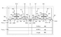
- FIG. 2is a cross sectional view of EEPROM cell 101 and peripheral transistors 201 and 202 .
- Peripheral transistors 201 - 202are located on the same chip as EEPROM cells 101 - 104 , and are typically used to access these EEPROM cells.
- Peripheral transistor 201includes a source 211 , a drain 212 , a control gate 210 , and a gate dielectric layer 213 .
- Gate dielectric layer 213has a first thickness T 1 , which is selected in view of a first voltage used to control the peripheral circuitry.
- thickness T 1can be 75 Angstroms or less, depending on the process.
- peripheral transistor 202includes a source 221 , a drain 222 , a control gate 220 , and a gate dielectric layer 223 .
- Gate dielectric layer 223has a second thickness T 2 , which is selected in view of a second voltage used to control the peripheral circuitry.
- thickness T 2can be 300 Angstroms to handle a control voltage of 15 Volts.
- Access transistor 111includes a gate dielectric layer 231 having the second thickness T 2 .
- a select gate SG 1is located over this gate dielectric layer 231 .
- NVM transistor 121includes a gate dielectric layer 232 , most of which has a thickness close to the second thickness T 2 .
- Dielectric layer 232includes a thin dielectric tunneling region 233 , which has a third thickness T 3 of about 100 Angstroms.
- a floating gate FG 1which stores charge, is located over gate dielectric layer 232 (including tunneling dielectric region 233 ).
- the tunneling dielectric region 233is located over a highly doped N+ region 235 , which is an extension of the n-type source/drain diffusion shared by access transistor 111 and NVM transistor 121 .
- An inter-poly dielectric layer 234having a thickness T 4 , is located over floating gate FG 1 .
- a control gate CG 1is located over the inter-poly dielectric layer 234 .
- the thickness T 4 of gate dielectric layer 234is selected in view of the voltages used to control NVM transistor 121 .
- the dielectric layer 234can be a composite dielectric (oxide-nitride-oxide) with an equivalent silicon dioxide thickness of about 200 Angstroms to handle programming voltages of about 15 Volts.
- EEPROM cells 102 - 104are identical to EEPROM cell 101 .
- a high programming voltage VPP(on the order of about 15 Volts) is applied to the control line CL 1 and the select line SL 1 .
- the drain terminals D 1 -D 2 and the source terminal S 12are grounded.
- the floating gates of NVM transistors 121 - 122are coupled to a fraction of the programming voltage VPP, which is enough to produce tunneling currents from the underlying diffusion extension region 235 through the thin gate dielectric region 233 . Consequently, the tunneling currents in NVM transistors 121 - 122 , will cause excess electrons to be trapped in the floating gates of these NVM transistors.
- EEPROM cells 101 - 102can be erased independently of EEPROM cells 103 - 104 . Alternately, EEPROM cells 103 - 104 can be erased at the same time as EEPROM cells 101 - 102 .
- the high programming voltage VPP(15 Volts), is applied to the drain terminal D 1 and to select line SL 1 .
- the control line CL 1 and the select line SL 2are grounded.
- the source terminal S 12 and drain D 2are left floating.
- access transistor 111is turned on, and the high programming voltage VPP is applied to the drain extension region 235 of NVM transistor 121 .
- the high voltage across the thin gate dielectric region 233causes electrons to be removed from the floating gate FG 1 , thereby causing this transistor to have a relatively low threshold voltage.
- the drain of access transistor 111must have a relatively large active region around the contact in order to properly receive the high programming voltage VPP.
- the select gate SG 1 of access transistor 111must be relatively large in order to properly receive the high programming voltage VPP.
- access transistor 111cannot be scaled for processes with feature size of less than 0.35 microns.
- the memory transistor 121has a large gate area, to accommodate the drain extension diffusion region 235 under the tunneling dielectric region 233 .
- access transistors 112 - 114 and memory transistors 122 - 124respectively. It would therefore be desirable to have an EEPROM system that can be scaled to sub-0.35 micron processes.
- the present inventionprovides a memory system that includes a column of EEPROM cells, including a first EEPROM cell having a first access transistor and a first NVM transistor, and a second EEPROM cell having a second access transistor and a second NVM transistor.
- the first access transistorhas a drain region that is continuous with the source region of the first NVM transistor
- the second access transistorhas a drain region that is continuous with the source region of the second NVM transistor.
- the first and second access transistorsshare a common source region.
- a first bit lineconnects the drain of the first NVM transistor and the drain of the second NVM transistor.
- First and second word linesare connected to the control gates of the first and second NVM transistors, respectively.
- First and second select linesare connected to the control gates of the first and second access transistors, respectively. Multiple columns can be combined to form an array of EEPROM cells.
- the EEPROM cellsare fabricated in a first well region, which in turn, is located in a second well region of an opposite conductivity type.
- the EEPROM cellsare made of n-channel access transistors and n-channel NVM transistors, then the EEPROM cells are fabricated in a p-well region.
- the p-well regionin turn, is located in an n-well region. Bias voltages are applied to the p-well and n-well regions in accordance with one embodiment of the present invention.
- the control gate of the first NVM transistori.e., the first word line
- a programming voltage V PPe.g. 15 Volts
- the first and second bit lines and the source lineare left in a floating state. Under these conditions, a tunneling current flows from the first well region to the floating gate of the first NVM transistor, thereby erasing the first NVM transistor. Any other NVM transistors coupled to the first word line are erased at the same time as the first NVM transistor.
- the second NVM transistor(and any other NVM transistors coupled to the second word line) can be erased at the same time as the first NVM transistor by grounding the second word line during the erase operation.
- the programming voltage V PPis applied to the control gate of the first NVM transistor, and the first and second well regions are grounded.
- the first bit linewhich corresponds to the cell selected to be programmed, is also grounded.
- the control gates of the first and second access transistors and the control gate of the second NVM transistorare grounded.
- the sources of the first and second access transistorsare left in a floating state. Under these conditions, a tunnel current flows from the floating gate of the first NVM transistor to the first well region, thereby programming this NVM transistor.
- Bit lines associated with columns that are not to be programmedare held at an intermediate voltage to prevent programming of EEPROM cells in these columns.
- the high programming voltageis not applied across the gate dielectric layers of the first and second access transistors during erase and program operations of the present invention.
- the gate dielectric layers of the first and second access transistorscan be made relatively thin.
- the high programming voltageis not applied to the bit lines or to the source lines, with respect to the underlying well. Consequently, the access transistors and the NVM transistors may be scaled to sub-0.35 micron processes.
- FIG. 1is a circuit diagram illustrating a conventional memory system that includes an array of electrically erasable and programmable memory (EEPROM) cells.
- EEPROMelectrically erasable and programmable memory
- FIG. 2is a cross sectional view of one of the EEPROM cells of FIG. 1 and a pair of peripheral transistors, which are located on the same chip.
- FIG. 3is a circuit diagram of a memory array, which includes a plurality of EEPROM cells, in accordance with one embodiment of the present invention.
- FIG. 4is a cross sectional view of two of the EEPROM cells of FIG. 3 in accordance with one embodiment of the present invention.
- FIG. 5is a circuit diagram illustrating an erase operation being performed to two of the EEPROM cells of FIG. 3 in accordance with one embodiment of the present invention.
- FIG. 6is a circuit diagram illustrating a programming operation being performed to an EEPROM cell of FIG. 3 in accordance with one embodiment of the present invention.
- FIG. 7is a circuit diagram illustrating a read operation of two of the EEPROM cells of FIG. 3 in accordance with one embodiment of the present invention.
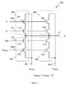
- FIG. 3is a circuit diagram of a 2 ⁇ 2 memory array 300 , which includes EEPROM cells 301 - 304 , in accordance with one embodiment of the present invention.
- EEPROM cells 301 and 302are located in a first row of memory array 300
- EEPROM cells 303 and 304are located in a second row of memory array 300
- EEPROM cells 301 and 303are located in a first column of memory array 300
- EEPROM cells 302 and 304are located in a second column of memory array 300 .
- Data wordsare written to (and read from) the various rows of memory array 300 .
- Each of the EEPROM cells 301 - 304includes an access transistor 311 - 314 , respectively, and an NVM transistor 321 - 324 , respectively.
- the source of each access transistor 311 - 314is commonly coupled to a source terminal S.
- the drains of access transistors 311 - 314are coupled to the sources of NVM transistors 321 - 324 , respectively.
- the drains of the NVM transistors in each columnare commonly coupled to a corresponding bit line.
- the drains of NVM transistors 321 and 323are coupled to bit line BL 1
- the drains of NVM transistors 322 and 324are coupled to bit line BL 2 .
- control gates of the NVM transistors in each roware commonly coupled to a corresponding word line.
- control gates of NVM transistors 321 and 322are coupled to word line WL 1
- control gates of NVM transistors 323 and 324are coupled to word line WL 2 .
- the select gates of the access transistors in each roware commonly coupled to a corresponding select line.
- the select gates of access transistors 301 and 302are coupled to select line S 1
- the select gates of access transistors 313 and 314are coupled to select line S 2 .
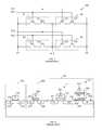
- FIG. 4is a cross sectional view of EEPROM cells 301 and 303 in accordance with one embodiment of the present invention.
- EEPROM cells 301 - 304are N-channel devices, which are fabricated in a P-well region 403 .
- the P-well region 403is contacted to receive a P-well bias voltage, V PWELL .
- the P-well region 403is fabricated in an N-well region 402 .
- the N-well region 402is contacted to receive an N-well bias voltage, V NWELL .
- the N-well region 402in turn is fabricated in a p-type semiconductor substrate 401 .
- NVM transistor 321includes n-type drain region 451 , n-type source/drain region 452 , gate dielectric 441 , floating gate 421 , inter-gate dielectric 445 , control gate 431 and dielectric sidewall spacers 461 - 462 .
- Drain region 451includes n+ contact region 451 A and lightly doped (n ⁇ ) drain region 451 B. Drain region 451 A is separated from the gate 421 , thus preventing high field disturb during programming.
- Salicide regions 471 and 472are formed on the upper surfaces of drain contact region 451 A and control gate 431 .
- inter-gate dielectric 445is a stacked oxide-nitride-oxide (ONO) structure.
- Access transistor 311includes n-type source/drain region 452 (which is shared with NVM transistor 321 ), source region 453 , gate dielectric 442 , control gate 411 and dielectric sidewall spacers 463 - 464 .
- Source region 453includes n+ contact region 453 A and lightly doped (n ⁇ ) regions 453 B- 453 C.
- Salicide regions 473 and 474are formed on the upper surfaces of control gate 411 and source contact region 453 A.
- Access transistor 313includes n-type source region 453 (which is shared with access transistor 311 ), n-type source/drain region 454 , gate dielectric 443 , control gate 412 and dielectric sidewall spacers 465 - 466 .
- Salicide region 475is formed on the upper surface of control gate 412 .
- NVM transistor 323includes n-type drain region 455 , n-type source/drain region 454 , gate dielectric 444 , floating gate 422 , inter-gate dielectric 446 , control gate 432 and dielectric sidewall spacers 467 - 468 .
- Drain region 455includes n+ contact region 455 A and lightly doped (n ⁇ ) drain region 455 B.
- Salicide layers 476 and 477are formed on the upper surfaces of control gate 432 and drain contact region 455 A.
- inter-gate dielectric 446is a stacked oxide-nitride-oxide (ONO) structure.
- EEPROM cells 302 and 304have the same construction as EEPROM cells 301 and 303 .
- Memory array 300operates as follows in accordance with one embodiment of the present invention.
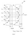
- FIG. 5is a circuit diagram illustrating an erase operation being performed to EEPROM cells 303 and 304 of memory array 300 .
- common source region S and bit lines BL 1 -BL 2are maintained in a floating state (i.e., not connected to any external voltage).
- Word line WL 1 , select lines S 1 -S 2 , P-well region 403 and N-well region 402are coupled to receive a high programming voltage V PP , on the order of about 15 Volts. That is, V PWELL and V NWELL are set equal to V PP .
- Word line WL 2which connects to the NVM transistors 323 - 324 selected for erase, is coupled to the ground voltage supply terminal.
- NVM transistor 323exhibits a relatively low threshold voltage. Because NVM transistor 324 is biased in the same manner as NVM transistor 323 , NVM transistor 324 is also erased. Note that all NVM transistors in the same row will be simultaneously erased.
- NVM transistors 321 and 322are not erased because word line WL 1 is held at the high voltage V PP .
- NVM transistors 321 and 322can be erased at the same time as NVM transistors 323 and 324 by coupling word line WL 1 to the ground voltage supply terminal (rather than the V PP programming voltage terminal).
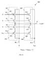
- FIG. 6is a circuit diagram illustrating a programming operation being performed to EEPROM cell 303 of memory array 300 .
- common source region Sis maintained in a floating state.
- Word line WL 2is coupled to receive the high programming voltage V PP .
- Select lines S 1 -S 2 , word line WL 1 , bit line BL 1 , P-well region 403 and N-well region 402are coupled to the ground voltage supply terminal.
- Bit line BL 2is coupled to receive an intermediate voltage V INT , on the order of about 5 Volts.
- NVM transistor 323exhibits a relatively high threshold voltage. Because the drain of NVM transistor 324 is biased with the intermediate voltage V INT , the voltage across the gate dielectric located between the drain and the floating gate of NVM transistor 324 is not high enough to induce a Fowler-Nordheim tunneling current. Consequently, NVM transistor 324 is not programmed. However, note that NVM transistor 324 could be programmed at the same time as NVM transistor 323 by connecting bit line BL 2 to the ground voltage supply terminal.
- NVM transistors 321 and 322are not disturbed because bit line potential is too low for Fowler-Nordheim tunneling. Moreover, there is no drain current through NVM transistors 321 and 322 because the word line WL 1 and the select line S 1 are held at the ground supply voltage. In an alternate example, NVM transistor 321 can be programmed at the same time as NVM transistor 323 by coupling word line WL 1 to receive the high voltage V PP .
- the high programming voltage V PPis not applied to the access transistors 311 - 314 during the programming operation.
- FIG. 7is a circuit diagram illustrating a read operation that accesses EEPROM cells 303 and 304 of memory array 300 .
- common source region S, word line WL 1 and select line S 1are coupled to the ground voltage supply terminal.
- access transistors 311 - 312 and NVM transistors 321 - 322are turned off.
- Select line S 2is coupled to receive the V DD supply voltage.
- access transistors 313 and 314are turned on.
- Word line WL 2is coupled to receive the read voltage V READ .
- the read voltage V READis selected to have a value that is large enough to turn on a corresponding NVM transistor that is in the erased state (i.e., in a low threshold voltage state).
- the read voltage V READis selected to be smaller than the minimum value which turns on a corresponding NVM transistor that is in the programmed state (i.e., in a high threshold voltage state).
- the read voltage V READis 2 Volts, but other values can be used in the range of 1 to 5 Volts.
- Bit lines BL 1 and BL 2are coupled to receive the read voltage V READ , or a value close to V READ in the same range of 1 to 5V.
- Sense amplifier circuits(not shown) are also coupled to bit lines BL 1 and BL 2 . These sense amplifiers latch a read data value having a first state if the current flowing on the corresponding bit line exceeds a threshold current value (i.e., if the corresponding NVM transistor is in an erased state). Conversely, these sense amplifiers latch a read data value having a second state if the current flowing on the corresponding bit line is less than the threshold current value (i.e., if the corresponding NVM transistor is in a programmed state).
- the high programming voltage V PPis not applied to any transistors during the read operation. Because the high programming voltage V PP is not applied to the drains, sources or select gates of access transistors 311 - 314 during the erase, program or read operations, these access transistors do not require thick gate oxide and do not require large spacing at diffusion contacts. As a result, memory array 300 can advantageously be scaled to sub-0.35 micron processes.
- the present inventionalso includes a process for fabricating the memory array 300 and the associated peripheral devices.
- this processis implemented as follows.
- a pad oxide layeris formed over a p-type monocrystalline silicon wafer having a ⁇ 100> crystalline structure.
- An N-well region maskis formed over the wafer.
- N-well implantsare then performed through the N-well mask, and the N-well mask is removed.
- the N-well implantis diffused at a depth of 3-5 microns in a high temperature furnace.
- a pad oxide layer and an overlying silicon nitride (Si 3 N 4 ) layerare then formed over the wafer surface.
- An active region maskwhich defines the locations of the active regions to be formed on the wafer, is then formed over the resulting structure.
- An etchis performed through the active region mask, thereby exposing the inactive regions of the wafer.
- the active region maskis then removed.
- Field oxideis then thermally grown in the inactive regions, to a thickness of about 500 nm.
- the pad oxide layer and silicon nitride layerare then removed, and a sacrificial oxide layer, having a thickness of about 30 nm, is formed over the upper surface of the wafer.
- a p-well maskwhich defines the locations of P-well regions (e.g., P-well region 403 ) to be formed in the wafer, is then formed over the resulting structure. P-well implants are then performed through the P-well mask, and the P-well mask is removed. The sacrificial oxide layer is then removed (e.g., by etching).
- a high voltage gate dielectric layeris then formed, in two steps, over the resulting structure.
- the high voltage gate dielectric layercan be, for example, thermally grown silicon oxide having a thickness of about 30 nm.
- the high voltage gate dielectric layeris used to form peripheral transistors that route the V PP programming voltage (15 Volts) to word lines WL 1 and WL 2 .
- a thinner oxideis grown, for example, to a thickness of about 25 nm.
- An intermediate voltage oxide maskis formed over the structure and the first step oxide is etched. The low voltage oxide mask is then removed.
- the intermediate voltage gate dielectric layeris then grown over the resulting structure, such that the intermediate voltage areas have an oxide of about 10 nm, while the remaining high voltage area has an oxide of about 30 nm.
- the intermediate voltage gate dielectric layeris used in transistors that operate in response to the intermediate voltage of 5 Volts.
- the intermediate voltage gate dielectric layeris used to form gate dielectric layers 442 and 443 of access transistors 311 and 313 , respectively, and gate dielectric layers 441 and 444 of NVM transistors 321 and 323 , respectively.
- the intermediate voltage gate dielectric layeris also used to form similar structures in access transistors 312 and 314 and NVM transistors 322 and 324 .
- the intermediate voltage gate dielectric layeris also used to form peripheral devices (e.g., transistors) which operate in response to an intermediate voltage.
- a first layer of polycrystalline silicon (polysilicon) having a thickness of 100-200 nmis then deposited over the gate dielectric layer.
- the first polysilicon layeris doped with a n-type impurity (N+), such that the first polysilicon layer becomes conductive.
- a silicon oxide-silicon nitride-silicon oxide (ONO) structureis then formed over the first polysilicon layer. This ONO structure is used in NVM transistors 321 - 324 (see, e.g., ONO structures 445 - 446 ).
- a first gate maskwhich defines the locations of the floating gates of NVM transistors 321 - 324 and of high-voltage peripheral transistors is then formed over the second dielectric layer.
- a dry etchis performed through the ONO dielectric and the first polysilicon layer and, thereby forming the control gates.
- the first gate maskis then removed.
- a low voltage oxide maskis then formed over the resulting structure.
- a threshold adjustmentis performed for the low voltage transistors and the intermediate oxide is etched.
- the low voltage oxide maskis then removed.
- a low voltage gate dielectric layeris then formed over the resulting structure.
- the low voltage gate dielectric layercan be, for example, thermally grown silicon oxide having a thickness of about 7 nm. In the described embodiments, the low voltage gate dielectric layer is used to form peripheral transistors that control the addressing of memory array 300 and all logic functions.
- a second layer of polysilicon having a thickness of 200-300 nmis then deposited over the ONO layer.
- the second polysilicon layeris doped with an n-type impurity (N+), such that the second polysilicon layer becomes conductive.
- a second gate maskwhich defines the locations of the low-voltage peripheral transistors, is then formed over the second layer of polysilicon.
- a dry etchis performed through the second polysilicon layer, thereby forming the gates of the low-voltage peripheral transistors.
- the second gate maskis then removed.
- a high voltage n-type lightly doped drain (HVNLDD) maskwhich defines the locations of the lightly doped n-type regions in memory array 300 (e.g., 451 B 452 , 453 B, 453 C, 454 and 455 B) and the lightly doped n-type regions in the high voltage n-channel peripheral transistors.
- An n-type LDD implantis performed through the HVNLDD mask, thereby forming the lightly doped drain regions of the high-voltage NMOS transistors.
- the HVNLDD maskis then removed.
- a low voltage n-type lightly doped drain (NLDD) maskwhich defines the locations of the lightly doped n-type regions the low voltage n-channel peripheral transistors.
- An n-type LDD implantis performed through the NLDD mask, thereby forming the lightly doped drain regions of the low-voltage peripheral NMOS transistors.
- the NLDD maskis then removed.
- a p-type lightly doped drain (PLDD) maskwhich defines the locations of the lightly doped p-type regions of the p-channel peripheral transistors.
- a p-type LDD implantis performed through the PLDD mask, thereby forming the lightly doped drain regions of the p-channel peripheral transistors.
- the PLDD maskis then removed.
- a sidewall dielectric layeris then deposited over the resulting structure.
- the sidewall dielectric layeris then etched, thereby forming dielectric sidewall spacers (e.g., sidewall spacers 461 - 468 ) adjacent to the various polysilicon structures.
- a n-type source/drain maskwhich defines the locations of the n-type source and drain contact regions (e.g., regions 451 A, 453 A and 455 A) is formed over the resulting structure.
- a n+ implantis performed through the n-type source/drain mask, thereby forming the n-type source/drain contact regions of the NMOS transistors.
- the n-type source/drain maskis then removed.
- a p-type source/drain maskwhich defines the locations of the p-type source and drain contact regions is formed over the resulting structure.
- a p+ implantis performed through the p-type source/drain mask, thereby forming the required p-type source/drain contact regions of the PMOS transistors.
- the p-type source/drain maskis then removed.
- a salicide maskwhich defines the locations where salicide should not be formed, is formed over the resulting structure.
- a layer of metal silicideis then deposited over the resulting structure.
- An anneal stepis then performed, thereby causing the metal silicide layer to react with underlying silicon regions, thereby forming self-aligned polysilicide (salicide).
- the unreacted portions of the metal silicide layerare then removed.
- the salicide maskis then removed.
- the back end processingis then performed, wherein: pad oxide/oxide is deposited over the resulting structure; BPSG deposition/flow is performed over the pad oxide/oxide; contact openings are formed through the pad oxide/oxide/BPSG; the contact openings are filled with conductive plugs; a first metal layer is deposited over the resulting structure and patterned; an inter-metal oxide layer is formed over the resulting structure; the inter-metal oxide is planarized by chemical mechanical polishing (CMP); vias are formed in the inter-metal oxide; the vias are filled by conductive plugs; a second metal layer is deposited and patterned; a bake is performed in the presence of hydrogen; and a passivation layer is deposited and patterned to expose the pads on the wafer.
- CMPchemical mechanical polishing
Landscapes
- Engineering & Computer Science (AREA)
- Microelectronics & Electronic Packaging (AREA)
- Non-Volatile Memory (AREA)
Abstract
Description
- The present invention relates to electrically erasable and programmable memory (EEPROM) cells.
FIG. 1 is a circuit diagram illustrating aconventional memory system 100 that includes a 2×2 array of electrically erasable and programmable memory (EEPROM) cells101-104. EEPROM cells101-104 include CMOS access transistors111-114, respectively, and non-volatile memory (NVM) transistors121-124, respectively. The drains ofaccess transistors access transistors FIG. 2 is a cross sectional view ofEEPROM cell 101 andperipheral transistors Peripheral transistor 201 includes asource 211, adrain 212, acontrol gate 210, and a gatedielectric layer 213. Gatedielectric layer 213 has a first thickness T1, which is selected in view of a first voltage used to control the peripheral circuitry. For example, thickness T1 can be 75 Angstroms or less, depending on the process. Similarly,peripheral transistor 202 includes asource 221, adrain 222, acontrol gate 220, and a gatedielectric layer 223. Gatedielectric layer 223 has a second thickness T2, which is selected in view of a second voltage used to control the peripheral circuitry. For example, thickness T2 can be 300 Angstroms to handle a control voltage of 15 Volts.Access transistor 111 includes a gatedielectric layer 231 having the second thickness T2. A select gate SG1 is located over this gatedielectric layer 231.NVM transistor 121 includes a gatedielectric layer 232, most of which has a thickness close to the second thickness T2.Dielectric layer 232 includes a thindielectric tunneling region 233, which has a third thickness T3 of about 100 Angstroms. A floating gate FG1, which stores charge, is located over gate dielectric layer232 (including tunneling dielectric region233). The tunnelingdielectric region 233 is located over a highlydoped N+ region 235, which is an extension of the n-type source/drain diffusion shared byaccess transistor 111 andNVM transistor 121. An inter-polydielectric layer 234, having a thickness T4, is located over floating gate FG1. A control gate CG1 is located over the inter-polydielectric layer 234. The thickness T4 of gatedielectric layer 234 is selected in view of the voltages used to controlNVM transistor 121. For example, thedielectric layer 234 can be a composite dielectric (oxide-nitride-oxide) with an equivalent silicon dioxide thickness of about 200 Angstroms to handle programming voltages of about 15 Volts. EEPROM cells102-104 are identical toEEPROM cell 101.- In order to erase
EEPROM cells diffusion extension region 235 through the thin gatedielectric region 233. Consequently, the tunneling currents in NVM transistors121-122, will cause excess electrons to be trapped in the floating gates of these NVM transistors. These trapped electrons increase the threshold voltages of NVM transistors121-122 (i.e., erase NVM transistors121-122). EEPROM cells101-102 can be erased independently of EEPROM cells103-104. Alternately, EEPROM cells103-104 can be erased at the same time as EEPROM cells101-102. - In order to program
EEPROM cell 101, the high programming voltage VPP (15 Volts), is applied to the drain terminal D1 and to select line SL1. The control line CL1 and the select line SL2 are grounded. The source terminal S12 and drain D2 are left floating. Under these conditions,access transistor 111 is turned on, and the high programming voltage VPP is applied to thedrain extension region 235 ofNVM transistor 121. The high voltage across the thin gatedielectric region 233 causes electrons to be removed from the floating gate FG1, thereby causing this transistor to have a relatively low threshold voltage. - The drain of
access transistor 111 must have a relatively large active region around the contact in order to properly receive the high programming voltage VPP. In addition, the select gate SG1 ofaccess transistor 111 must be relatively large in order to properly receive the high programming voltage VPP. As a result,access transistor 111 cannot be scaled for processes with feature size of less than 0.35 microns. Similarly, thememory transistor 121 has a large gate area, to accommodate the drainextension diffusion region 235 under the tunnelingdielectric region 233. The same limitations apply to access transistors112-114 and memory transistors122-124, respectively. It would therefore be desirable to have an EEPROM system that can be scaled to sub-0.35 micron processes. - Accordingly, the present invention provides a memory system that includes a column of EEPROM cells, including a first EEPROM cell having a first access transistor and a first NVM transistor, and a second EEPROM cell having a second access transistor and a second NVM transistor. The first access transistor has a drain region that is continuous with the source region of the first NVM transistor, and the second access transistor has a drain region that is continuous with the source region of the second NVM transistor. The first and second access transistors share a common source region. A first bit line connects the drain of the first NVM transistor and the drain of the second NVM transistor. First and second word lines are connected to the control gates of the first and second NVM transistors, respectively. First and second select lines are connected to the control gates of the first and second access transistors, respectively. Multiple columns can be combined to form an array of EEPROM cells.
- The EEPROM cells are fabricated in a first well region, which in turn, is located in a second well region of an opposite conductivity type. For example, if the EEPROM cells are made of n-channel access transistors and n-channel NVM transistors, then the EEPROM cells are fabricated in a p-well region. The p-well region, in turn, is located in an n-well region. Bias voltages are applied to the p-well and n-well regions in accordance with one embodiment of the present invention.
- To erase the first NVM transistor, the control gate of the first NVM transistor (i.e., the first word line) is grounded, and a programming voltage VPP(e.g., 15 Volts) is applied to the first and second well regions, the first and second select lines, and the second word line (assuming that the second NVM transistor is not to be erased). The first and second bit lines and the source line are left in a floating state. Under these conditions, a tunneling current flows from the first well region to the floating gate of the first NVM transistor, thereby erasing the first NVM transistor. Any other NVM transistors coupled to the first word line are erased at the same time as the first NVM transistor. The second NVM transistor (and any other NVM transistors coupled to the second word line) can be erased at the same time as the first NVM transistor by grounding the second word line during the erase operation.
- To program the first EEPROM cell, the programming voltage VPPis applied to the control gate of the first NVM transistor, and the first and second well regions are grounded. The first bit line, which corresponds to the cell selected to be programmed, is also grounded. The control gates of the first and second access transistors and the control gate of the second NVM transistor are grounded. The sources of the first and second access transistors are left in a floating state. Under these conditions, a tunnel current flows from the floating gate of the first NVM transistor to the first well region, thereby programming this NVM transistor. Bit lines associated with columns that are not to be programmed are held at an intermediate voltage to prevent programming of EEPROM cells in these columns.
- Advantageously, the high programming voltage is not applied across the gate dielectric layers of the first and second access transistors during erase and program operations of the present invention. Thus, the gate dielectric layers of the first and second access transistors can be made relatively thin. Similarly, the high programming voltage is not applied to the bit lines or to the source lines, with respect to the underlying well. Consequently, the access transistors and the NVM transistors may be scaled to sub-0.35 micron processes.
- The present invention will be more fully understood in view of the following description and drawings.
FIG. 1 is a circuit diagram illustrating a conventional memory system that includes an array of electrically erasable and programmable memory (EEPROM) cells.FIG. 2 is a cross sectional view of one of the EEPROM cells ofFIG. 1 and a pair of peripheral transistors, which are located on the same chip.FIG. 3 is a circuit diagram of a memory array, which includes a plurality of EEPROM cells, in accordance with one embodiment of the present invention.FIG. 4 is a cross sectional view of two of the EEPROM cells ofFIG. 3 in accordance with one embodiment of the present invention.FIG. 5 is a circuit diagram illustrating an erase operation being performed to two of the EEPROM cells ofFIG. 3 in accordance with one embodiment of the present invention.FIG. 6 is a circuit diagram illustrating a programming operation being performed to an EEPROM cell ofFIG. 3 in accordance with one embodiment of the present invention.FIG. 7 is a circuit diagram illustrating a read operation of two of the EEPROM cells ofFIG. 3 in accordance with one embodiment of the present invention.FIG. 3 is a circuit diagram of a 2×2memory array 300, which includes EEPROM cells301-304, in accordance with one embodiment of the present invention. Although a 2×2 memory array is described in the following embodiments, it is understood that this memory array can be easily expanded to implement larger arrays. In the described embodiments,EEPROM cells memory array 300, andEEPROM cells memory array 300.EEPROM cells memory array 300, andEEPROM cells memory array 300. Data words are written to (and read from) the various rows ofmemory array 300.- Each of the EEPROM cells301-304 includes an access transistor311-314, respectively, and an NVM transistor321-324, respectively. The source of each access transistor311-314 is commonly coupled to a source terminal S. The drains of access transistors311-314 are coupled to the sources of NVM transistors321-324, respectively. The drains of the NVM transistors in each column are commonly coupled to a corresponding bit line. Thus, the drains of
NVM transistors NVM transistors - The control gates of the NVM transistors in each row are commonly coupled to a corresponding word line. Thus, the control gates of
NVM transistors NVM transistors - The select gates of the access transistors in each row are commonly coupled to a corresponding select line. Thus, the select gates of
access transistors access transistors FIG. 4 is a cross sectional view ofEEPROM cells well region 403. The P-well region 403 is contacted to receive a P-well bias voltage, VPWELL. The P-well region 403, in turn, is fabricated in an N-well region 402. The N-well region 402 is contacted to receive an N-well bias voltage, VNWELL. The N-well region 402, in turn is fabricated in a p-type semiconductor substrate 401.NVM transistor 321 includes n-type drain region 451, n-type source/drain region 452,gate dielectric 441, floatinggate 421,inter-gate dielectric 445,control gate 431 and dielectric sidewall spacers461-462.Drain region 451 includesn+ contact region 451A and lightly doped (n−)drain region 451B.Drain region 451A is separated from thegate 421, thus preventing high field disturb during programming.Salicide regions drain contact region 451A andcontrol gate 431. In the described embodiment,inter-gate dielectric 445 is a stacked oxide-nitride-oxide (ONO) structure.Access transistor 311 includes n-type source/drain region452 (which is shared with NVM transistor321),source region 453,gate dielectric 442,control gate 411 and dielectric sidewall spacers463-464.Source region 453 includesn+ contact region 453A and lightly doped (n−)regions 453B-453C.Salicide regions control gate 411 andsource contact region 453A.Access transistor 313 includes n-type source region453 (which is shared with access transistor311), n-type source/drain region 454,gate dielectric 443,control gate 412 and dielectric sidewall spacers465-466.Salicide region 475 is formed on the upper surface ofcontrol gate 412.NVM transistor 323 includes n-type drain region 455, n-type source/drain region 454,gate dielectric 444, floatinggate 422,inter-gate dielectric 446,control gate 432 and dielectric sidewall spacers467-468.Drain region 455 includesn+ contact region 455A and lightly doped (n−)drain region 455B. Salicide layers476 and477 are formed on the upper surfaces ofcontrol gate 432 anddrain contact region 455A. In the described embodiment,inter-gate dielectric 446 is a stacked oxide-nitride-oxide (ONO) structure.- Although not illustrated in
FIG. 4 ,EEPROM cells EEPROM cells Memory array 300 operates as follows in accordance with one embodiment of the present invention. FIG. 5 is a circuit diagram illustrating an erase operation being performed toEEPROM cells memory array 300. During this erase operation, common source region S and bit lines BL1-BL2 are maintained in a floating state (i.e., not connected to any external voltage). Word line WL1, select lines S1-S2, P-well region 403 and N-well region 402 are coupled to receive a high programming voltage VPP, on the order of about 15 Volts. That is, VPWELLand VNWELLare set equal to VPP. Word line WL2, which connects to the NVM transistors323-324 selected for erase, is coupled to the ground voltage supply terminal.- Under these conditions, a large voltage (VPP) exists between the P-
well region 403 and thecontrol gate 432 ofNVM transistor 323. As a result, a Fowler-Nordheim tunneling current is introduced between P-well region 403 and floatinggate 422, which is coupled to the high voltage on thecontrol gate 432 ofNVM transistor 323, such that excess electrons are removed from floatinggate 422. At the end of the erase operation,NVM transistor 323 exhibits a relatively low threshold voltage. BecauseNVM transistor 324 is biased in the same manner asNVM transistor 323,NVM transistor 324 is also erased. Note that all NVM transistors in the same row will be simultaneously erased. - In the described example,
NVM transistors NVM transistors NVM transistors - Note that all drain and source diffusions will acquire a potential close to the voltage of P-well403, so that the junction bias' associated with these diffusions is close to zero. Also, the high programming voltage VPPis not applied between any terminals of the access transistors311-314 during the erase operation.
FIG. 6 is a circuit diagram illustrating a programming operation being performed toEEPROM cell 303 ofmemory array 300. During this programming operation, common source region S is maintained in a floating state. Word line WL2 is coupled to receive the high programming voltage VPP. Select lines S1-S2, word line WL1, bit line BL1, P-well region 403 and N-well region 402 are coupled to the ground voltage supply terminal. Bit line BL2 is coupled to receive an intermediate voltage VINT, on the order of about 5 Volts.- Under these conditions, a large voltage (a large fraction of VPP) exists between the channel region below gate dielectric444 (which has the same potential as drain region455) and the floating
gate 422 ofNVM transistor 323. As a result, a Fowler-Nordheim tunneling current flows betweendrain region 455 and floatinggate 422 ofNVM transistor 323, such that electrons are trapped on floatinggate 422. At the end of the programming operation,NVM transistor 323 exhibits a relatively high threshold voltage. Because the drain ofNVM transistor 324 is biased with the intermediate voltage VINT, the voltage across the gate dielectric located between the drain and the floating gate ofNVM transistor 324 is not high enough to induce a Fowler-Nordheim tunneling current. Consequently,NVM transistor 324 is not programmed. However, note thatNVM transistor 324 could be programmed at the same time asNVM transistor 323 by connecting bit line BL2 to the ground voltage supply terminal. - In the described example,
NVM transistors NVM transistors NVM transistor 321 can be programmed at the same time asNVM transistor 323 by coupling word line WL1 to receive the high voltage VPP. - Note that the high programming voltage VPPis not applied to the access transistors311-314 during the programming operation.
FIG. 7 is a circuit diagram illustrating a read operation that accessesEEPROM cells memory array 300. During this read operation, common source region S, word line WL1 and select line S1 are coupled to the ground voltage supply terminal. As a result, access transistors311-312 and NVM transistors321-322 are turned off. Select line S2 is coupled to receive the VDDsupply voltage. As a result,access transistors - Bit lines BL1 and BL2 are coupled to receive the read voltage VREAD, or a value close to VREADin the same range of 1 to 5V. Sense amplifier circuits (not shown) are also coupled to bit lines BL1 and BL2. These sense amplifiers latch a read data value having a first state if the current flowing on the corresponding bit line exceeds a threshold current value (i.e., if the corresponding NVM transistor is in an erased state). Conversely, these sense amplifiers latch a read data value having a second state if the current flowing on the corresponding bit line is less than the threshold current value (i.e., if the corresponding NVM transistor is in a programmed state).
- Note that the high programming voltage VPPis not applied to any transistors during the read operation. Because the high programming voltage VPPis not applied to the drains, sources or select gates of access transistors311-314 during the erase, program or read operations, these access transistors do not require thick gate oxide and do not require large spacing at diffusion contacts. As a result,
memory array 300 can advantageously be scaled to sub-0.35 micron processes. - The present invention also includes a process for fabricating the
memory array 300 and the associated peripheral devices. In accordance with one embodiment, this process is implemented as follows. A pad oxide layer is formed over a p-type monocrystalline silicon wafer having a <100> crystalline structure. An N-well region mask is formed over the wafer. N-well implants are then performed through the N-well mask, and the N-well mask is removed. The N-well implant is diffused at a depth of 3-5 microns in a high temperature furnace. After removing the N-well oxide, a pad oxide layer and an overlying silicon nitride (Si3N4) layer are then formed over the wafer surface. An active region mask, which defines the locations of the active regions to be formed on the wafer, is then formed over the resulting structure. An etch is performed through the active region mask, thereby exposing the inactive regions of the wafer. The active region mask is then removed. Field oxide is then thermally grown in the inactive regions, to a thickness of about 500 nm. The pad oxide layer and silicon nitride layer are then removed, and a sacrificial oxide layer, having a thickness of about 30 nm, is formed over the upper surface of the wafer. - A p-well mask, which defines the locations of P-well regions (e.g., P-well region403) to be formed in the wafer, is then formed over the resulting structure. P-well implants are then performed through the P-well mask, and the P-well mask is removed. The sacrificial oxide layer is then removed (e.g., by etching).
- A high voltage gate dielectric layer is then formed, in two steps, over the resulting structure. The high voltage gate dielectric layer can be, for example, thermally grown silicon oxide having a thickness of about 30 nm. In the described embodiments, the high voltage gate dielectric layer is used to form peripheral transistors that route the VPPprogramming voltage (15 Volts) to word lines WL1 and WL2. In the first step, a thinner oxide is grown, for example, to a thickness of about 25 nm. An intermediate voltage oxide mask is formed over the structure and the first step oxide is etched. The low voltage oxide mask is then removed. An intermediate voltage gate dielectric layer is then grown over the resulting structure, such that the intermediate voltage areas have an oxide of about 10 nm, while the remaining high voltage area has an oxide of about 30 nm. In the described embodiments, the intermediate voltage gate dielectric layer is used in transistors that operate in response to the intermediate voltage of 5 Volts. For example, the intermediate voltage gate dielectric layer is used to form gate
dielectric layers access transistors dielectric layers NVM transistors access transistors NVM transistors - A first layer of polycrystalline silicon (polysilicon) having a thickness of 100-200 nm is then deposited over the gate dielectric layer. The first polysilicon layer is doped with a n-type impurity (N+), such that the first polysilicon layer becomes conductive. A silicon oxide-silicon nitride-silicon oxide (ONO) structure is then formed over the first polysilicon layer. This ONO structure is used in NVM transistors321-324 (see, e.g., ONO structures445-446).
- A first gate mask, which defines the locations of the floating gates of NVM transistors321-324 and of high-voltage peripheral transistors is then formed over the second dielectric layer. A dry etch is performed through the ONO dielectric and the first polysilicon layer and, thereby forming the control gates. The first gate mask is then removed.
- A low voltage oxide mask is then formed over the resulting structure. A threshold adjustment is performed for the low voltage transistors and the intermediate oxide is etched. The low voltage oxide mask is then removed. A low voltage gate dielectric layer is then formed over the resulting structure. The low voltage gate dielectric layer can be, for example, thermally grown silicon oxide having a thickness of about 7 nm. In the described embodiments, the low voltage gate dielectric layer is used to form peripheral transistors that control the addressing of
memory array 300 and all logic functions. - A second layer of polysilicon having a thickness of 200-300 nm is then deposited over the ONO layer. The second polysilicon layer is doped with an n-type impurity (N+), such that the second polysilicon layer becomes conductive.
- A second gate mask, which defines the locations of the low-voltage peripheral transistors, is then formed over the second layer of polysilicon. A dry etch is performed through the second polysilicon layer, thereby forming the gates of the low-voltage peripheral transistors. The second gate mask is then removed.
- A high voltage n-type lightly doped drain (HVNLDD) mask, which defines the locations of the lightly doped n-type regions in memory array300 (e.g.,
451 B - A low voltage n-type lightly doped drain (NLDD) mask, which defines the locations of the lightly doped n-type regions the low voltage n-channel peripheral transistors. An n-type LDD implant is performed through the NLDD mask, thereby forming the lightly doped drain regions of the low-voltage peripheral NMOS transistors. The NLDD mask is then removed.
- A p-type lightly doped drain (PLDD) mask, which defines the locations of the lightly doped p-type regions of the p-channel peripheral transistors. A p-type LDD implant is performed through the PLDD mask, thereby forming the lightly doped drain regions of the p-channel peripheral transistors. The PLDD mask is then removed.
- A sidewall dielectric layer is then deposited over the resulting structure. The sidewall dielectric layer is then etched, thereby forming dielectric sidewall spacers (e.g., sidewall spacers461-468) adjacent to the various polysilicon structures.
- A n-type source/drain mask, which defines the locations of the n-type source and drain contact regions (e.g.,
regions - A p-type source/drain mask, which defines the locations of the p-type source and drain contact regions is formed over the resulting structure. A p+ implant is performed through the p-type source/drain mask, thereby forming the required p-type source/drain contact regions of the PMOS transistors. The p-type source/drain mask is then removed.
- A salicide mask, which defines the locations where salicide should not be formed, is formed over the resulting structure. A layer of metal silicide is then deposited over the resulting structure. An anneal step is then performed, thereby causing the metal silicide layer to react with underlying silicon regions, thereby forming self-aligned polysilicide (salicide). The unreacted portions of the metal silicide layer are then removed. The salicide mask is then removed.
- The back end processing is then performed, wherein: pad oxide/oxide is deposited over the resulting structure; BPSG deposition/flow is performed over the pad oxide/oxide; contact openings are formed through the pad oxide/oxide/BPSG; the contact openings are filled with conductive plugs; a first metal layer is deposited over the resulting structure and patterned; an inter-metal oxide layer is formed over the resulting structure; the inter-metal oxide is planarized by chemical mechanical polishing (CMP); vias are formed in the inter-metal oxide; the vias are filled by conductive plugs; a second metal layer is deposited and patterned; a bake is performed in the presence of hydrogen; and a passivation layer is deposited and patterned to expose the pads on the wafer.
- Although the invention has been described in connection with several embodiments, it is understood that this invention is not limited to the embodiments disclosed, but is capable of various modifications, which would be apparent to one of ordinary skill in the art. Accordingly, the present invention is only limited by the following claims.
Claims (21)
Priority Applications (4)
| Application Number | Priority Date | Filing Date | Title |
|---|---|---|---|
| US11/278,103US7547944B2 (en) | 2006-03-30 | 2006-03-30 | Scalable electrically eraseable and programmable memory (EEPROM) cell array |
| US12/207,320US20090003074A1 (en) | 2006-03-30 | 2008-09-09 | Scalable Electrically Eraseable And Programmable Memory (EEPROM) Cell Array |
| US12/366,569US8093650B2 (en) | 2006-03-30 | 2009-02-05 | Scalable electrically eraseable and programmable memory (EEPROM) cell array |
| US12/389,972US7920424B2 (en) | 2006-03-30 | 2009-02-20 | Scalable electrically eraseable and programmable memory (EEPROM) cell array |
Applications Claiming Priority (1)
| Application Number | Priority Date | Filing Date | Title |
|---|---|---|---|
| US11/278,103US7547944B2 (en) | 2006-03-30 | 2006-03-30 | Scalable electrically eraseable and programmable memory (EEPROM) cell array |
Related Child Applications (3)
| Application Number | Title | Priority Date | Filing Date |
|---|---|---|---|
| US12/207,320Continuation-In-PartUS20090003074A1 (en) | 2006-03-30 | 2008-09-09 | Scalable Electrically Eraseable And Programmable Memory (EEPROM) Cell Array |
| US12/366,569ContinuationUS8093650B2 (en) | 2006-03-30 | 2009-02-05 | Scalable electrically eraseable and programmable memory (EEPROM) cell array |
| US12/389,972DivisionUS7920424B2 (en) | 2006-03-30 | 2009-02-20 | Scalable electrically eraseable and programmable memory (EEPROM) cell array |
Publications (2)
| Publication Number | Publication Date |
|---|---|
| US20070228451A1true US20070228451A1 (en) | 2007-10-04 |
| US7547944B2 US7547944B2 (en) | 2009-06-16 |
Family
ID=38557530
Family Applications (3)
| Application Number | Title | Priority Date | Filing Date |
|---|---|---|---|
| US11/278,103ActiveUS7547944B2 (en) | 2006-03-30 | 2006-03-30 | Scalable electrically eraseable and programmable memory (EEPROM) cell array |
| US12/366,569ActiveUS8093650B2 (en) | 2006-03-30 | 2009-02-05 | Scalable electrically eraseable and programmable memory (EEPROM) cell array |
| US12/389,972Active2026-07-10US7920424B2 (en) | 2006-03-30 | 2009-02-20 | Scalable electrically eraseable and programmable memory (EEPROM) cell array |
Family Applications After (2)
| Application Number | Title | Priority Date | Filing Date |
|---|---|---|---|
| US12/366,569ActiveUS8093650B2 (en) | 2006-03-30 | 2009-02-05 | Scalable electrically eraseable and programmable memory (EEPROM) cell array |
| US12/389,972Active2026-07-10US7920424B2 (en) | 2006-03-30 | 2009-02-20 | Scalable electrically eraseable and programmable memory (EEPROM) cell array |
Country Status (1)
| Country | Link |
|---|---|
| US (3) | US7547944B2 (en) |
Cited By (12)
| Publication number | Priority date | Publication date | Assignee | Title |
|---|---|---|---|---|
| US20080165582A1 (en)* | 2006-09-05 | 2008-07-10 | Catalyst Semiconductor, Inc. | Scalable Electrically Eraseable And Programmable Memory |
| US20090003074A1 (en)* | 2006-03-30 | 2009-01-01 | Catalyst Semiconductor, Inc. | Scalable Electrically Eraseable And Programmable Memory (EEPROM) Cell Array |
| US20090135649A1 (en)* | 2006-03-30 | 2009-05-28 | Catalyst Semiconductor, Inc. | Scalable Electrically Eraseable And Programmable Memory (EEPROM) Cell Array |
| CN103137194A (en)* | 2011-11-23 | 2013-06-05 | 上海华虹Nec电子有限公司 | Memory cell circuit structure of flash memory |
| US8750041B2 (en) | 2006-09-05 | 2014-06-10 | Semiconductor Components Industries, Llc | Scalable electrically erasable and programmable memory |
| CN107482009A (en)* | 2016-06-07 | 2017-12-15 | 中芯国际集成电路制造(上海)有限公司 | A kind of semiconductor devices and preparation method thereof, electronic installation |
| CN110649102A (en)* | 2018-06-27 | 2020-01-03 | 力旺电子股份有限公司 | Programmable Erasable Non-Volatile Memory |
| CN114023754A (en)* | 2022-01-10 | 2022-02-08 | 广州粤芯半导体技术有限公司 | Non-volatile flash memory and erasing method thereof |
| US11316011B2 (en)* | 2019-12-11 | 2022-04-26 | Ememory Technology Inc. | Erasable programmable non-volatile memory |
| CN114613775A (en)* | 2022-05-16 | 2022-06-10 | 广州粤芯半导体技术有限公司 | Non-volatile memory and its layout |
| US20230119398A1 (en)* | 2021-10-14 | 2023-04-20 | Ememory Technology Inc. | Erasable programmable single-poly non-volatile memory cell and associated array structure |
| US11972800B2 (en)* | 2021-12-16 | 2024-04-30 | Ememory Technology Inc. | Non-volatile memory cell and non-volatile memory cell array |
Families Citing this family (6)
| Publication number | Priority date | Publication date | Assignee | Title |
|---|---|---|---|---|
| US8320191B2 (en) | 2007-08-30 | 2012-11-27 | Infineon Technologies Ag | Memory cell arrangement, method for controlling a memory cell, memory array and electronic device |
| WO2010046873A1 (en)* | 2008-10-23 | 2010-04-29 | Nxp B.V. | Multi-transistor memory cell |
| US8228726B2 (en)* | 2008-12-14 | 2012-07-24 | Chip Memory Technology, Inc. | N-channel SONOS non-volatile memory for embedded in logic |
| JP2012191455A (en)* | 2011-03-10 | 2012-10-04 | Toshiba Corp | Semiconductor integrated circuit |
| US8923049B2 (en) | 2011-09-09 | 2014-12-30 | Aplus Flash Technology, Inc | 1T1b and 2T2b flash-based, data-oriented EEPROM design |
| US9041078B1 (en)* | 2013-12-17 | 2015-05-26 | Taiwan Semiconductor Manufacturing Company, Ltd. | Three-dimensional integrated circuit with inter-layer vias and intra-layer coupled transistors |
Citations (14)
| Publication number | Priority date | Publication date | Assignee | Title |
|---|---|---|---|---|
| US5364806A (en)* | 1991-08-29 | 1994-11-15 | Hyundai Electronics Industries Co., Ltd. | Method of making a self-aligned dual-bit split gate (DSG) flash EEPROM cell |
| US5862082A (en)* | 1998-04-16 | 1999-01-19 | Xilinx, Inc. | Two transistor flash EEprom cell and method of operating same |
| US5940324A (en)* | 1997-02-07 | 1999-08-17 | National Semiconductor Corporation | Single-poly EEPROM cell that is programmable and erasable in a low-voltage environment |
| US6107659A (en)* | 1997-09-05 | 2000-08-22 | Mitsubishi Denki Kabushiki Kaisha | Nonvolatile semiconductor memory device operable at high speed with low power supply voltage while preventing overerasing/overwriting |
| US6177315B1 (en)* | 1999-05-28 | 2001-01-23 | National Semiconductor Corporation | Method of fabricating a high density EEPROM array |
| US6420754B2 (en)* | 2000-02-28 | 2002-07-16 | Hitachi, Ltd. | Semiconductor integrated circuit device |
| US20030057474A1 (en)* | 1999-12-10 | 2003-03-27 | Ma Yueh Yale | Method of operation of a dual-bit double-polysilicon source-side injection flash EEPROM cell |
| US20030127684A1 (en)* | 2002-01-07 | 2003-07-10 | Hyun-Khe Yoo | Split-gate type nonvolatile memory devices and methods for fabricating the same |
| US20040047217A1 (en)* | 2002-07-09 | 2004-03-11 | Eiji Kamiya | Non-volatile semiconductor memory device and method of manufacturing the same |
| US20050133851A1 (en)* | 2003-12-17 | 2005-06-23 | Micron Technology, Inc. | Vertical NAND flash memory array |
| US20050184337A1 (en)* | 2004-02-24 | 2005-08-25 | Micron Technology, Inc. | 4f2 eeprom nrom memory arrays with vertical devices |
| US7006381B2 (en)* | 2001-11-27 | 2006-02-28 | Koninklijke Philips Electronics N.V. | Semiconductor device having a byte-erasable EEPROM memory |
| US7157771B2 (en)* | 2004-01-30 | 2007-01-02 | Micron Technology, Inc. | Vertical device 4F2 EEPROM memory |
| US7274075B2 (en)* | 2001-01-31 | 2007-09-25 | Kabushiki Kaisha Toshiba | Nonvolatile semiconductor memory device having pair of selection transistors with different source and drain impurity concentrations and with different channel dopant concentrations |
Family Cites Families (20)
| Publication number | Priority date | Publication date | Assignee | Title |
|---|---|---|---|---|
| JPH0745730A (en)* | 1993-02-19 | 1995-02-14 | Sgs Thomson Microelettronica Spa | Two-level polysilicon eeprom memory cell as well as its programming method and manufacture, integrated eeprom memory circuit, eeprom memory cell and its programming method |
| US5648669A (en)* | 1995-05-26 | 1997-07-15 | Cypress Semiconductor | High speed flash memory cell structure and method |
| US5914514A (en)* | 1996-09-27 | 1999-06-22 | Xilinx, Inc. | Two transistor flash EPROM cell |
| US5790455A (en)* | 1997-01-02 | 1998-08-04 | John Caywood | Low voltage single supply CMOS electrically erasable read-only memory |
| US6420753B1 (en)* | 1997-06-30 | 2002-07-16 | Winbond Memory Laboratory | Electrically selectable and alterable memory cells |
| US6040216A (en)* | 1997-08-11 | 2000-03-21 | Mosel Vitelic, Inc. | Method (and device) for producing tunnel silicon oxynitride layer |
| US6081451A (en)* | 1998-04-01 | 2000-06-27 | National Semiconductor Corporation | Memory device that utilizes single-poly EPROM cells with CMOS compatible programming voltages |
| US6274898B1 (en)* | 1999-05-21 | 2001-08-14 | Vantis Corporation | Triple-well EEPROM cell using P-well for tunneling across a channel |
| US6757196B1 (en)* | 2001-03-22 | 2004-06-29 | Aplus Flash Technology, Inc. | Two transistor flash memory cell for use in EEPROM arrays with a programmable logic device |
| FR2826496A1 (en)* | 2001-06-25 | 2002-12-27 | St Microelectronics Sa | Memory store of type EEPROM protected against the effects of a breakdown of an access transistor |
| KR100456541B1 (en)* | 2002-01-04 | 2004-11-09 | 삼성전자주식회사 | Non volatile memory device and method of fabricating the same |
| US7630237B2 (en)* | 2003-02-06 | 2009-12-08 | Sandisk Corporation | System and method for programming cells in non-volatile integrated memory devices |
| JP4163610B2 (en)* | 2003-12-22 | 2008-10-08 | 株式会社東芝 | Nonvolatile semiconductor memory device |
| CN100461424C (en)* | 2003-12-30 | 2009-02-11 | 中芯国际集成电路制造(上海)有限公司 | Structure and Method for Designing Tunnel Oxidation Window Region of Semiconductor Integrated Circuit |
| JP4757476B2 (en)* | 2004-10-29 | 2011-08-24 | 富士通セミコンダクター株式会社 | Semiconductor device |
| DE602006004396D1 (en)* | 2005-05-18 | 2009-02-05 | St Microelectronics Sa | EEPROM memory architecture |
| US7547944B2 (en)* | 2006-03-30 | 2009-06-16 | Catalyst Semiconductor, Inc. | Scalable electrically eraseable and programmable memory (EEPROM) cell array |
| US7590005B2 (en)* | 2006-04-06 | 2009-09-15 | Macronix International Co., Ltd. | Program and erase methods with substrate transient hot carrier injections in a non-volatile memory |
| US7450418B2 (en)* | 2006-04-12 | 2008-11-11 | Ememory Technology Inc. | Non-volatile memory and operating method thereof |
| US7528436B2 (en) | 2006-09-05 | 2009-05-05 | Catalyst Semiconductor, Inc. | Scalable electrically eraseable and programmable memory |
- 2006
- 2006-03-30USUS11/278,103patent/US7547944B2/enactiveActive
- 2009
- 2009-02-05USUS12/366,569patent/US8093650B2/enactiveActive
- 2009-02-20USUS12/389,972patent/US7920424B2/enactiveActive
Patent Citations (16)
| Publication number | Priority date | Publication date | Assignee | Title |
|---|---|---|---|---|
| US5364806A (en)* | 1991-08-29 | 1994-11-15 | Hyundai Electronics Industries Co., Ltd. | Method of making a self-aligned dual-bit split gate (DSG) flash EEPROM cell |
| US5940324A (en)* | 1997-02-07 | 1999-08-17 | National Semiconductor Corporation | Single-poly EEPROM cell that is programmable and erasable in a low-voltage environment |
| US6107659A (en)* | 1997-09-05 | 2000-08-22 | Mitsubishi Denki Kabushiki Kaisha | Nonvolatile semiconductor memory device operable at high speed with low power supply voltage while preventing overerasing/overwriting |
| US5862082A (en)* | 1998-04-16 | 1999-01-19 | Xilinx, Inc. | Two transistor flash EEprom cell and method of operating same |
| US6177315B1 (en)* | 1999-05-28 | 2001-01-23 | National Semiconductor Corporation | Method of fabricating a high density EEPROM array |
| US20030057474A1 (en)* | 1999-12-10 | 2003-03-27 | Ma Yueh Yale | Method of operation of a dual-bit double-polysilicon source-side injection flash EEPROM cell |
| US6420754B2 (en)* | 2000-02-28 | 2002-07-16 | Hitachi, Ltd. | Semiconductor integrated circuit device |
| US7274075B2 (en)* | 2001-01-31 | 2007-09-25 | Kabushiki Kaisha Toshiba | Nonvolatile semiconductor memory device having pair of selection transistors with different source and drain impurity concentrations and with different channel dopant concentrations |
| US7006381B2 (en)* | 2001-11-27 | 2006-02-28 | Koninklijke Philips Electronics N.V. | Semiconductor device having a byte-erasable EEPROM memory |
| US20030127684A1 (en)* | 2002-01-07 | 2003-07-10 | Hyun-Khe Yoo | Split-gate type nonvolatile memory devices and methods for fabricating the same |
| US20040047217A1 (en)* | 2002-07-09 | 2004-03-11 | Eiji Kamiya | Non-volatile semiconductor memory device and method of manufacturing the same |
| US20050133851A1 (en)* | 2003-12-17 | 2005-06-23 | Micron Technology, Inc. | Vertical NAND flash memory array |
| US7148538B2 (en)* | 2003-12-17 | 2006-12-12 | Micron Technology, Inc. | Vertical NAND flash memory array |
| US7157771B2 (en)* | 2004-01-30 | 2007-01-02 | Micron Technology, Inc. | Vertical device 4F2 EEPROM memory |
| US20050184337A1 (en)* | 2004-02-24 | 2005-08-25 | Micron Technology, Inc. | 4f2 eeprom nrom memory arrays with vertical devices |
| US20050265063A1 (en)* | 2004-02-24 | 2005-12-01 | Micron Technology, Inc. | 4F2 EEPROM NROM memory arrays with vertical devices |
Cited By (19)
| Publication number | Priority date | Publication date | Assignee | Title |
|---|---|---|---|---|
| US20090003074A1 (en)* | 2006-03-30 | 2009-01-01 | Catalyst Semiconductor, Inc. | Scalable Electrically Eraseable And Programmable Memory (EEPROM) Cell Array |
| US20090135649A1 (en)* | 2006-03-30 | 2009-05-28 | Catalyst Semiconductor, Inc. | Scalable Electrically Eraseable And Programmable Memory (EEPROM) Cell Array |
| US20090196105A1 (en)* | 2006-03-30 | 2009-08-06 | Catalyst Semiconductor, Inc. | Scalable Electrically Eraseable And Programmable Memory (EEPROM) Cell Array |
| US7920424B2 (en) | 2006-03-30 | 2011-04-05 | Semiconductor Components Industries, L.L.C. | Scalable electrically eraseable and programmable memory (EEPROM) cell array |
| US8093650B2 (en) | 2006-03-30 | 2012-01-10 | Semiconductor Components Industries, L.L.C. | Scalable electrically eraseable and programmable memory (EEPROM) cell array |
| US8139408B2 (en) | 2006-09-05 | 2012-03-20 | Semiconductor Components Industries, L.L.C. | Scalable electrically eraseable and programmable memory |
| US20080165582A1 (en)* | 2006-09-05 | 2008-07-10 | Catalyst Semiconductor, Inc. | Scalable Electrically Eraseable And Programmable Memory |
| US8750041B2 (en) | 2006-09-05 | 2014-06-10 | Semiconductor Components Industries, Llc | Scalable electrically erasable and programmable memory |
| TWI496151B (en)* | 2008-03-18 | 2015-08-11 | Semiconductor Components Ind | Expandable erasable and programmable memory |
| WO2009117219A1 (en)* | 2008-03-18 | 2009-09-24 | Catalyst Semiconductor, Inc. | Scalable electrically eraseable and programmable memory |
| CN103137194A (en)* | 2011-11-23 | 2013-06-05 | 上海华虹Nec电子有限公司 | Memory cell circuit structure of flash memory |
| CN107482009A (en)* | 2016-06-07 | 2017-12-15 | 中芯国际集成电路制造(上海)有限公司 | A kind of semiconductor devices and preparation method thereof, electronic installation |
| CN110649102A (en)* | 2018-06-27 | 2020-01-03 | 力旺电子股份有限公司 | Programmable Erasable Non-Volatile Memory |
| US11316011B2 (en)* | 2019-12-11 | 2022-04-26 | Ememory Technology Inc. | Erasable programmable non-volatile memory |
| US20230119398A1 (en)* | 2021-10-14 | 2023-04-20 | Ememory Technology Inc. | Erasable programmable single-poly non-volatile memory cell and associated array structure |
| US11818887B2 (en)* | 2021-10-14 | 2023-11-14 | Ememory Technology Inc. | Erasable programmable single-poly non-volatile memory cell and associated array structure |
| US11972800B2 (en)* | 2021-12-16 | 2024-04-30 | Ememory Technology Inc. | Non-volatile memory cell and non-volatile memory cell array |
| CN114023754A (en)* | 2022-01-10 | 2022-02-08 | 广州粤芯半导体技术有限公司 | Non-volatile flash memory and erasing method thereof |
| CN114613775A (en)* | 2022-05-16 | 2022-06-10 | 广州粤芯半导体技术有限公司 | Non-volatile memory and its layout |
Also Published As
| Publication number | Publication date |
|---|---|
| US20090196105A1 (en) | 2009-08-06 |
| US8093650B2 (en) | 2012-01-10 |
| US7920424B2 (en) | 2011-04-05 |
| US20090135649A1 (en) | 2009-05-28 |
| US7547944B2 (en) | 2009-06-16 |
Similar Documents
| Publication | Publication Date | Title |
|---|---|---|
| US7547944B2 (en) | Scalable electrically eraseable and programmable memory (EEPROM) cell array | |
| US20090003074A1 (en) | Scalable Electrically Eraseable And Programmable Memory (EEPROM) Cell Array | |
| US6903422B2 (en) | Semiconductor integrated circuits, fabrication method for the same and semiconductor integrated circuit systems | |
| US6312990B1 (en) | Structure nonvolatile semiconductor memory cell array and method for fabricating same | |
| US8344443B2 (en) | Single poly NVM devices and arrays | |
| US5953254A (en) | Serial flash memory | |
| US7087953B2 (en) | Unified non-volatile memory device and method for integrating NOR and NAND-type flash memory and EEPROM device on a single substrate | |
| US6157575A (en) | Nonvolatile memory device and operating method thereof | |
| JP4463954B2 (en) | Nonvolatile memory device having bulk bias contact structure in cell array region | |
| US20070257305A1 (en) | Nonvolatile semiconductor memory device and manufacturing method thereof | |
| US6365457B1 (en) | Method for manufacturing nonvolatile memory device using self-aligned source process | |
| US20080165582A1 (en) | Scalable Electrically Eraseable And Programmable Memory | |
| US7528436B2 (en) | Scalable electrically eraseable and programmable memory | |
| US20110032766A1 (en) | N-channel sonos non-volatile memory for embedded in logic | |
| US8134201B2 (en) | Semiconductor memory device provided with stacked layer gate including charge accumulation layer and control gate, and manufacturing method thereof | |
| US20080237696A1 (en) | Alignment protection in non-volatile memory and array | |
| US8649226B2 (en) | Nonvolatile semiconductor memory device and erasing method of nonvolatile semiconductor memory device | |
| US6380031B1 (en) | Method to form an embedded flash memory circuit with reduced process steps | |
| US20060268607A1 (en) | Operation method of non-volatile memory structure | |
| US20080061355A1 (en) | Method of reducing memory cell size for floating gate NAND flash | |
| US10388660B2 (en) | Semiconductor device and method for manufacturing the same | |
| US7217964B1 (en) | Method and apparatus for coupling to a source line in a memory device | |
| US6429093B1 (en) | Sidewall process for forming a low resistance source line | |
| JP3940477B2 (en) | Semiconductor device | |
| US6060356A (en) | Method of fabricating virtual ground SSI flash EPROM cell and array |
Legal Events
| Date | Code | Title | Description |
|---|---|---|---|
| AS | Assignment | Owner name:CATALYST SEMICONDUCTOR, INC., CALIFORNIA Free format text:ASSIGNMENT OF ASSIGNORS INTEREST;ASSIGNORS:GEORGESCU, SORIN S;COSMIN, ADAM P;REEL/FRAME:017553/0258 Effective date:20060330 | |
| AS | Assignment | Owner name:JPMORGAN CHASE BANK, N.A., NEW YORK Free format text:SECURITY AGREEMENT;ASSIGNOR:CATALYST SEMICONDUCTOR, INC.;REEL/FRAME:021744/0171 Effective date:20081010 Owner name:JPMORGAN CHASE BANK, N.A.,NEW YORK Free format text:SECURITY AGREEMENT;ASSIGNOR:CATALYST SEMICONDUCTOR, INC.;REEL/FRAME:021744/0171 Effective date:20081010 | |
| STCF | Information on status: patent grant | Free format text:PATENTED CASE | |
| AS | Assignment | Owner name:SEMICONDUCTOR COMPONENTS INDUSTRIES, L.L.C., ARIZO Free format text:MERGER;ASSIGNOR:CATALYST SEMICONDUCTOR, INC.;REEL/FRAME:023180/0479 Effective date:20090827 Owner name:SEMICONDUCTOR COMPONENTS INDUSTRIES, L.L.C.,ARIZON Free format text:MERGER;ASSIGNOR:CATALYST SEMICONDUCTOR, INC.;REEL/FRAME:023180/0479 Effective date:20090827 | |
| FPAY | Fee payment | Year of fee payment:4 | |
| AS | Assignment | Owner name:DEUTSCHE BANK AG NEW YORK BRANCH, NEW YORK Free format text:SECURITY INTEREST;ASSIGNOR:SEMICONDUCTOR COMPONENTS INDUSTRIES, LLC;REEL/FRAME:038620/0087 Effective date:20160415 | |
| AS | Assignment | Owner name:SEMICONDUCTOR COMPONENTS INDUSTRIES, LLC, ARIZONA Free format text:RELEASE BY SECURED PARTY;ASSIGNOR:JPMORGAN CHASE BANK, N.A., AS ADMINISTRATIVE AGENT AND COLLATERAL AGENT;REEL/FRAME:038631/0345 Effective date:20100511 Owner name:SEMICONDUCTOR COMPONENTS INDUSTRIES, LLC, ARIZONA Free format text:RELEASE BY SECURED PARTY;ASSIGNOR:JPMORGAN CHASE BANK, N.A. (ON ITS BEHALF AND ON BEHALF OF ITS PREDECESSOR IN INTEREST, CHASE MANHATTAN BANK);REEL/FRAME:038632/0074 Effective date:20160415 | |
| AS | Assignment | Owner name:DEUTSCHE BANK AG NEW YORK BRANCH, AS COLLATERAL AG Free format text:CORRECTIVE ASSIGNMENT TO CORRECT THE INCORRECT PATENT NUMBER 5859768 AND TO RECITE COLLATERAL AGENT ROLE OF RECEIVING PARTY IN THE SECURITY INTEREST PREVIOUSLY RECORDED ON REEL 038620 FRAME 0087. ASSIGNOR(S) HEREBY CONFIRMS THE SECURITY INTEREST;ASSIGNOR:SEMICONDUCTOR COMPONENTS INDUSTRIES, LLC;REEL/FRAME:039853/0001 Effective date:20160415 Owner name:DEUTSCHE BANK AG NEW YORK BRANCH, AS COLLATERAL AGENT, NEW YORK Free format text:CORRECTIVE ASSIGNMENT TO CORRECT THE INCORRECT PATENT NUMBER 5859768 AND TO RECITE COLLATERAL AGENT ROLE OF RECEIVING PARTY IN THE SECURITY INTEREST PREVIOUSLY RECORDED ON REEL 038620 FRAME 0087. ASSIGNOR(S) HEREBY CONFIRMS THE SECURITY INTEREST;ASSIGNOR:SEMICONDUCTOR COMPONENTS INDUSTRIES, LLC;REEL/FRAME:039853/0001 Effective date:20160415 | |
| FPAY | Fee payment | Year of fee payment:8 | |
| MAFP | Maintenance fee payment | Free format text:PAYMENT OF MAINTENANCE FEE, 12TH YEAR, LARGE ENTITY (ORIGINAL EVENT CODE: M1553); ENTITY STATUS OF PATENT OWNER: LARGE ENTITY Year of fee payment:12 | |
| AS | Assignment | Owner name:FAIRCHILD SEMICONDUCTOR CORPORATION, ARIZONA Free format text:RELEASE OF SECURITY INTEREST IN PATENTS RECORDED AT REEL 038620, FRAME 0087;ASSIGNOR:DEUTSCHE BANK AG NEW YORK BRANCH, AS COLLATERAL AGENT;REEL/FRAME:064070/0001 Effective date:20230622 Owner name:SEMICONDUCTOR COMPONENTS INDUSTRIES, LLC, ARIZONA Free format text:RELEASE OF SECURITY INTEREST IN PATENTS RECORDED AT REEL 038620, FRAME 0087;ASSIGNOR:DEUTSCHE BANK AG NEW YORK BRANCH, AS COLLATERAL AGENT;REEL/FRAME:064070/0001 Effective date:20230622 |