US20070228415A1 - Semiconductor device and manufacturing method thereof - Google Patents
Semiconductor device and manufacturing method thereofDownload PDFInfo
- Publication number
- US20070228415A1 US20070228415A1US11/476,205US47620506AUS2007228415A1US 20070228415 A1US20070228415 A1US 20070228415A1US 47620506 AUS47620506 AUS 47620506AUS 2007228415 A1US2007228415 A1US 2007228415A1
- Authority
- US
- United States
- Prior art keywords
- layer
- electrode
- semiconductor device
- tantalum
- aluminum
- Prior art date
- Legal status (The legal status is an assumption and is not a legal conclusion. Google has not performed a legal analysis and makes no representation as to the accuracy of the status listed.)
- Granted
Links
Images


Classifications
- H—ELECTRICITY
- H10—SEMICONDUCTOR DEVICES; ELECTRIC SOLID-STATE DEVICES NOT OTHERWISE PROVIDED FOR
- H10D—INORGANIC ELECTRIC SEMICONDUCTOR DEVICES
- H10D62/00—Semiconductor bodies, or regions thereof, of devices having potential barriers
- H10D62/80—Semiconductor bodies, or regions thereof, of devices having potential barriers characterised by the materials
- H10D62/85—Semiconductor bodies, or regions thereof, of devices having potential barriers characterised by the materials being Group III-V materials, e.g. GaAs
- H10D62/8503—Nitride Group III-V materials, e.g. AlN or GaN
- H—ELECTRICITY
- H01—ELECTRIC ELEMENTS
- H01L—SEMICONDUCTOR DEVICES NOT COVERED BY CLASS H10
- H01L21/00—Processes or apparatus adapted for the manufacture or treatment of semiconductor or solid state devices or of parts thereof
- H01L21/02—Manufacture or treatment of semiconductor devices or of parts thereof
- H01L21/04—Manufacture or treatment of semiconductor devices or of parts thereof the devices having potential barriers, e.g. a PN junction, depletion layer or carrier concentration layer
- H01L21/18—Manufacture or treatment of semiconductor devices or of parts thereof the devices having potential barriers, e.g. a PN junction, depletion layer or carrier concentration layer the devices having semiconductor bodies comprising elements of Group IV of the Periodic Table or AIIIBV compounds with or without impurities, e.g. doping materials
- H01L21/28—Manufacture of electrodes on semiconductor bodies using processes or apparatus not provided for in groups H01L21/20 - H01L21/268
- H01L21/283—Deposition of conductive or insulating materials for electrodes conducting electric current
- H01L21/285—Deposition of conductive or insulating materials for electrodes conducting electric current from a gas or vapour, e.g. condensation
- H01L21/28506—Deposition of conductive or insulating materials for electrodes conducting electric current from a gas or vapour, e.g. condensation of conductive layers
- H01L21/28575—Deposition of conductive or insulating materials for electrodes conducting electric current from a gas or vapour, e.g. condensation of conductive layers on semiconductor bodies comprising AIIIBV compounds
- H—ELECTRICITY
- H10—SEMICONDUCTOR DEVICES; ELECTRIC SOLID-STATE DEVICES NOT OTHERWISE PROVIDED FOR
- H10D—INORGANIC ELECTRIC SEMICONDUCTOR DEVICES
- H10D30/00—Field-effect transistors [FET]
- H10D30/40—FETs having zero-dimensional [0D], one-dimensional [1D] or two-dimensional [2D] charge carrier gas channels
- H10D30/47—FETs having zero-dimensional [0D], one-dimensional [1D] or two-dimensional [2D] charge carrier gas channels having 2D charge carrier gas channels, e.g. nanoribbon FETs or high electron mobility transistors [HEMT]
- H10D30/471—High electron mobility transistors [HEMT] or high hole mobility transistors [HHMT]
- H10D30/475—High electron mobility transistors [HEMT] or high hole mobility transistors [HHMT] having wider bandgap layer formed on top of lower bandgap active layer, e.g. undoped barrier HEMTs such as i-AlGaN/GaN HEMTs
- H10D30/4755—High electron mobility transistors [HEMT] or high hole mobility transistors [HHMT] having wider bandgap layer formed on top of lower bandgap active layer, e.g. undoped barrier HEMTs such as i-AlGaN/GaN HEMTs having wide bandgap charge-carrier supplying layers, e.g. modulation doped HEMTs such as n-AlGaAs/GaAs HEMTs
- H—ELECTRICITY
- H10—SEMICONDUCTOR DEVICES; ELECTRIC SOLID-STATE DEVICES NOT OTHERWISE PROVIDED FOR
- H10D—INORGANIC ELECTRIC SEMICONDUCTOR DEVICES
- H10D62/00—Semiconductor bodies, or regions thereof, of devices having potential barriers
- H10D62/80—Semiconductor bodies, or regions thereof, of devices having potential barriers characterised by the materials
- H10D62/85—Semiconductor bodies, or regions thereof, of devices having potential barriers characterised by the materials being Group III-V materials, e.g. GaAs
- H—ELECTRICITY
- H10—SEMICONDUCTOR DEVICES; ELECTRIC SOLID-STATE DEVICES NOT OTHERWISE PROVIDED FOR
- H10D—INORGANIC ELECTRIC SEMICONDUCTOR DEVICES
- H10D64/00—Electrodes of devices having potential barriers
- H10D64/20—Electrodes characterised by their shapes, relative sizes or dispositions
- H10D64/23—Electrodes carrying the current to be rectified, amplified, oscillated or switched, e.g. sources, drains, anodes or cathodes
- H10D64/251—Source or drain electrodes for field-effect devices
- H—ELECTRICITY
- H10—SEMICONDUCTOR DEVICES; ELECTRIC SOLID-STATE DEVICES NOT OTHERWISE PROVIDED FOR
- H10D—INORGANIC ELECTRIC SEMICONDUCTOR DEVICES
- H10D64/00—Electrodes of devices having potential barriers
- H10D64/60—Electrodes characterised by their materials
- H10D64/62—Electrodes ohmically coupled to a semiconductor
Definitions
- the present inventionrelates to a semiconductor device and manufacturing method thereof suitable for use in, for example, a gallium nitride based field effect transistor (GaNFET).
- GaNFETgallium nitride based field effect transistor
- GaNFETgallium nitride field effect transistor
- GaNis highly promising as a material of a high power output device for which a high voltage operation is required.
- a GaNFEThas a structure, for example as shown in FIG. 5 , in which a GaN electron transit layer 2 and an Al x Ga 1-x N (0 ⁇ x ⁇ 1) electron supply layer 3 are formed in order on a substrate 1 and a gate electrode 5 , a source electrode 6 , and a drain electrode 7 are provided on the Al x Ga 1-x N (0 ⁇ x ⁇ 1) electron supply layer 3 .
- symbol 4denotes an SiN passivation film.
- a Ti/Al electrode or a Ti/Al/Ni/Au electrodeis mainly used as the source electrode 6 and the drain electrode 7 (that is, an ohmic electrode) provided on the Al x Ga 1-x N (0 ⁇ x ⁇ 1) electron supply layer 3 .
- the Ti/Al electrode or the Ti/Al/Ni/Au electrodeWhen the Ti/Al electrode or the Ti/Al/Ni/Au electrode is used, a compound is generated at an interface between Ti and Al at the time of annealing to obtain the ohmic properties, and the melting point of the compound is not so high. Further, at the time of annealing, metal condenses, irregularities are formed, and the electrode surface becomes coarse [refer to FIG. 6(A) to FIG. 6(D) ]. Furthermore, during operation at high temperatures, the Al atom, which is an electrode constituting element, moves (electromigration). These constitute factors that make the ohmic properties unstable at the time of device process or during operation at high temperatures.
- the inventors of the present inventionhave proposed one having a Ta/Al lamination structure as an ohmic electrode (for example, refer to Japanese Patent Application No. 2004-353460).
- FIG. 7(A) and FIG. 7(B)we have proposed to configure a GaNFET by forming the GaN electron transit layer 2 , the Al x Ga 1-x N (0 ⁇ x ⁇ 1) electron supply layer 3 , and an n-type GaN layer 8 in order on an SiC substrate 11 , providing the gate electrode 5 on the n-type GaN layer 8 , and providing the source electrode 6 and the drain electrode 7 having a structure (Ta/Al stacked structure) in which a tantalum (Ta) layer 9 and an aluminum (Al) layer 10 are stacked in order on the Al x Ga 1-x N (0 ⁇ x ⁇ 1) electron supply layer 3 .
- symbol 4denotes an SiN passivation film.
- the Ta/Al stacked structure for the source electrode 6 and the drain electrode 7as an ohmic electrode, it has been made possible to realize sufficient reliability in a high temperature environment.
- aluminum (Al)turns into aluminum hydroxide by reacting with water in the atmosphere. Since the aluminum hydroxide has a volume three times that of aluminum (Al), damage may be given to the portion (not shown) that covers the surface of the ohmic electrodes 6 and 7 of the SiN passivation film 4 .
- aspects of the present inventioncan provide a semiconductor device and manufacturing method thereof that have been made capable of improving reliability of an ohmic electrode in a high humidity environment while securing sufficient reliability of an ohmic electrode in a high temperature environment.
- a semiconductor devicecomprises a substrate, an n-type semiconductor layer or an undoped semiconductor layer on the substrate, and an ohmic electrode on the n-type semiconductor layer or the undoped semiconductor layer, wherein the ohmic electrode comprises a tantalum layer formed on the n-type semiconductor layer or the undoped semiconductor layer, an aluminum layer formed on the tantalum layer, and a metal layer formed on the aluminum layer and made of any one material of tantalum, nickel, palladium, and molybdenum.
- a method for manufacturing a semiconductor devicecomprises the steps of: forming at least an n-type semiconductor layer or an undoped semiconductor layer on a substrate; forming a tantalum layer, an aluminum layer, and a metal layer made of any one material of tantalum, nickel, palladium, and molybdenum in order on the n-type semiconductor layer or the undoped semiconductor layer; and annealing at temperatures lower than 600° C., and thus forming an ohmic electrode.
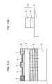
- FIG. 1(A)is a schematic section view showing a configuration of a semiconductor device according to an embodiment of the present invention, also showing its entire configuration.
- FIG. 1(B)is a schematic section view showing a configuration of a semiconductor device according to an embodiment of the present invention, also showing a portion of a source electrode or a drain electrode in its enlarged view.
- FIG. 2is a schematic section view showing a configuration of a semiconductor device according to a modification example of an embodiment of the present invention, also showing a part of a source electrode or a drain electrode in its enlarged view.
- FIG. 3(A) to FIG. 3(J)are schematic section views for explaining a method for manufacturing a semiconductor device according to an embodiment of the present invention.
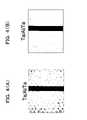
- FIG. 4(A)is a photo instead of a diagram showing an electrode surface of a semiconductor device according to an embodiment of the present invention in its partially enlarged view.
- FIG. 4(B)is a diagram schematically showing the photo in FIG. 4(A) .
- FIG. 5is a schematic section view showing a configuration of a conventional semiconductor device.
- FIG. 6(A)is a photo instead of a diagram showing an electrode surface of a conventional semiconductor device.
- FIG. 6(B)is a diagram showing a part of FIG. 6(A) in its enlarged view.
- FIG. 6(C) and FIG. 6(D)are diagrams schematically showing the photos in FIG. 6(A) and FIG. 6(B) , respectively.
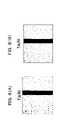
- FIG. 7(A)is a schematic section view showing a configuration of a semiconductor device proposed in the course of development of the present invention, also showing its entire configuration.
- FIG. 7(B)is a schematic section view showing a configuration of a semiconductor device proposed in the course of development of the present invention, also showing a part of a source electrode or a drain electrode in its enlarged view.
- FIG. 8(A)is a photo instead of a diagram showing an electrode surface of a semiconductor device proposed in the course of development of the present invention in its partially enlarged view.
- FIG. 8(B)is a diagram schematically showing the photo in FIG. 8(A) .
- FIG. 1(A) , FIG. 1(B) , FIG. 2 , and FIG. 3(A) to FIG. 3(J)are described below with reference to FIG. 1(A) , FIG. 1(B) , FIG. 2 , and FIG. 3(A) to FIG. 3(J) .
- the semiconductor deviceis, for example, a gallium nitride based field effect transistor (GaNFET; here, HEMT; High Electron Mobility Transistor), and has, for example as shown in FIG. 1(A) and FIG. 1(B) , a structure in which an intentionally undoped GaN electron transit layer 2 (i-GaN layer) 2 , an electron supply layer 3 made of an n-type Al x Ga 1-x N (0 ⁇ x ⁇ 1) layer (n-AlGaN layer), and an n-type GaN layer (n-GaN layer) 8 are stacked in order on an SiC (silicon carbide) substrate 11 .
- a spacer layerfor example, an intentionally undoped Al x Ga 1-x N (0 ⁇ x ⁇ 1) layer (i-AlGaN layer)] may be provided between the electron transit layer 2 and the electron supply layer 3 .
- a gate electrode 5is provided on the n-type GaN layer (n-GaN layer) 8 .
- the gate electrode 5is in Schottky contact with the n-GaN layer 8 .
- a source electrode 12 and a drain electrode 13are provided on the Al x Ga 1-x N (0 ⁇ x ⁇ 1) electron supply layer 3 (that is, n-type GaN based semiconductor layer; n-type III-V group nitride compound semiconductor layer).
- both the source electrode 12 and the drain electrode 13are in ohmic contact with the Al x Ga 1-x N (0 ⁇ x ⁇ 1) electron supply layer 3 .
- symbol 4denotes an SiN passivation film.
- both the source electrode 12 and the drain electrode 13are configured so as to have, for example, a Ta/Al/Ta stacked structure in which a tantalum (Ta) layer (first layer) 9 , an aluminum (Al) layer (second layer) 10 , and the tantalum (Ta) layer (third layer) 9 are stacked in order, as shown in FIG. 1(B) .
- an SiC substrate(high resistance substrate, semi-insulating substrate) having a resistivity of 1 ⁇ 10 6 ⁇ cm or more is used as the SiC substrate 11 .
- the substrateis not limited to this and for example, a conductive substrate (low resistance substrate; for example, metal substrate) having a resistivity of 1 ⁇ 10 5 ⁇ cm or less may be used.
- the structure of the source electrode 12 and the drain electrode 13 as an ohmic electrodeis not limited to this but it is only required to configure so as to have a structure in which a metal layer made of any one material of tantalum (Ta), palladium (Pd), nickel (Ni), and molybdenum (Mo) is stacked on the Ta/Al stacked structure in which the tantalum (Ta) layer 9 and the aluminum (Al) layer 10 are stacked in order.
- both the source electrode 12 and the drain electrode 13may also be possible to configure both the source electrode 12 and the drain electrode 13 so as to have a Ta/Al/Pd stacked structure in which the tantalum (Ta) layer 9 , the aluminum (Al) layer 10 , and a palladium (Pd) layer 14 are stacked in order.
- both the source electrode 12 and the drain electrode 13so as to have a Ta/Al/Ni stacked structure in which the tantalum (Ta) layer 9 , the aluminum (Al) layer 10 , and a nickel (Ni) layer are stacked in order, or configure both the source electrode 12 and the drain electrode 13 so as to have a Ta/Al/Mo stacked structure in which the tantalum (Ta) layer 9 , the aluminum (Al) layer 10 , and the molybdenum (Mo) layer are stacked in order.
- a part of the source electrode 12 or the drain electrode 13is shown in its enlarged view.
- the aluminum layer 10reacts with the metal layer at the time of annealing and a compound layer of the material that forms the metal layer and aluminum is generated at the interface between the aluminum layer 10 and the metal layer as a result.
- the semiconductor devicecomprises the compound layer of the material that forms the metal layer and aluminum between the aluminum layer 10 and the metal layer.
- the reason that the source electrode 12 and the drain electrode 13 as an ohmic electrode are configured as described above in the present embodimentis as follows.
- tantalum (Ta)has a melting point as extremely high as about 3,000° C. and is excellent in thermal stability, and the work function thereof is smaller than that of titanium (Ti).
- a compound generated when tantalum (Ta) and aluminum (Al) react with each otherhas a melting point higher than that of a compound generated when titanium (Ti) and aluminum (Al) react with each other. Therefore, tantalum (Ta) is used instead of titanium (Ti) conventionally used. Due to this, it is possible to improve the thermal stability and mechanical strength of the ohmic electrodes 12 and 13 considerably. In particular, it is possible to realize the ohmic electrodes 12 and 13 excellent in the long-term reliability in a high temperature environment.
- Materials having a high melting pointinclude tungsten, however, it is rather difficult to continuously evaporate tungsten for formation using, for example, the electron beam-physical vapor deposition (EB-PVD), therefore, tantalum (Ta) is used taking into consideration the easiness in handling during process.
- EB-PVDelectron beam-physical vapor deposition
- Tatantalum
- the reason that a Ta/Al stacked structure is employedis in order to suppress electromigration of the Al atom during operation at high temperatures by forming the tantalum layer 9 having a high melting point below the aluminum layer 10 .
- the tantalum layer 9 and the aluminum layer 10react with each other at the time of annealing and a compound layer of them is generated as a result at the interface between the tantalum layer 9 and the aluminum layer 10 .
- the semiconductor devicecomprises, as a result, the compound layer of tantalum and aluminum between the tantalum layer 9 and the aluminum layer 10 .
- the margin of the processis extended by forming the metal layer using a metal material, the melting point of the metal alone of which is high, the melting point of which is still high even after turning into a compound by reacting with aluminum (Al), and which has moisture resistance, on the Ta/Al stacked structure.
- the source electrode 12 and the drain electrode 13 as an ohmic electrodeare configured so as to have a Ta/Al/Ta stacked structure
- a structureis constructed in which the aluminum (Al) layer 10 is sandwiched in the vertical direction by the tantalum (Ta) layers 9 having the same coefficient of thermal expansion, therefore, when annealing is performed, for example, at temperatures below 600° C. (preferably, in the range of 530° C. to 570° C., or most preferably, 550° C.) in order to obtain the ohmic properties, the thermal stresses of the upper and lower tantalum (Ta) layers 9 are cancelled and an effect can be obtained that hillocks are prevented from occurring in the aluminum (Al) layer 10 by thermal cycle.
- Materials having a high melting pointinclude tungsten, however, it is rather difficult to continuously evaporate tungsten for formation using, for example, the electron beam-physical vapor deposition (EB-PVD), therefore, anyone of tantalum (Ta), palladium (Pd), nickel (Ni), and molybdenum (Mo) is used taking into consideration the easiness in handling during process.
- EB-PVDelectron beam-physical vapor deposition
- the intentionally undoped GaN electron transit layer 2(for example, 3 ⁇ m in thickness), the electron supply layer 3 made of an n-type Al 0.25 Ga 0.75 N layer (n-AlGaN layer; for example, 20 nm in thickness; Si doping concentration of 2 ⁇ 10 18 cm ⁇ 3 ), and the n-GaN layer 8 [for example, 10 nm or less in thickness (for example, 5 nm); Si doping concentration of 2 ⁇ 10 18 cm ⁇ 3 ] are stacked in order on the SiC (silicon carbide) substrate 11 to form a stacked structure using the normal metal organic chemical vapor deposition (MOVPE) method.
- MOVPEnormal metal organic chemical vapor deposition
- a spacer layer[intentionally undoped Al 0.25 Ga 0.75 N layer (i-AlGaN layer; for example, 3 nm in thickness)] may be provided between the electron transit layer 2 and the electron supply layer 3 .
- the configuration of the n-GaN layer 8is not limited to this and it is only necessary to use one doped with n-type impurity materials of 1 ⁇ 017 cm ⁇ 3 or more.
- separation between elementsis performed by, for example, applying a resist 15 and performing ion implantation to make both sides inactive. Separation between elements may be performed by removing both sides by etching.
- the source electrode 12 and the drain electrode 13 as an ohmic electrodeare formed using the deposition lift-off method.
- resists (here, two layers) 15 A and 15 Bare applied to the entire surface, patterning is performed so that an opening is formed in a source electrode formation scheduled region and a drain electrode formation scheduled region, respectively.
- the portion of the n-GaN layer 8which forms the source electrode 12 and the drain electrode 13 , is removed by the dry etching method using, for example, a chlorine based gas (for example, Cl 2 gas) or an inert gas.
- a chlorine based gasfor example, Cl 2 gas
- tantalum (Ta) 9for example, 10 nm in thickness
- aluminum (Al) 10for example, 280 nm in thickness
- tantalum (Ta) 9for example, 10 nm in thickness
- the source electrode 12 and the drain electrode 13 having a Ta/Al/Ta stacked structureare formed.
- annealingis performed at temperatures below 600° C. (preferably, in the range of 530° C. to 570° C., or most preferably, 550° C.) in order to obtain the ohmic properties and thus the source electrode 12 and the drain electrode 13 as an ohmic electrode that come into ohmic contact with the n-AlGaN layer are formed.
- the metalbecomes more unlikely to condense and the electrode surface does not become coarse, and an excellent and flat surface can be obtained [refer to FIG. 4(A) and FIG. 4(B) ].
- a gate electrodeis formed on the n-GaN layer 8 using the deposition lift-off method.
- nickel (Ni) 16 and gold (Au) 17are evaporated in order.
- the gate electrode 5having a Ni/Au stacked structure in which the nickel (Ni) layer 16 and the gold (Au) layer 17 are stacked.
- the SiN passivation film 4is deposited and formed having a thickness of, for example, 10 nm on the entire surface using, for example, the chemical vapor deposition (CVD) method.
- CVDchemical vapor deposition
- part of the SiN passivation film 4 on the source electrode 12 and the drain electrode 13is removed and a wire is provided so as to be connected to the source electrode 12 and the drain electrode 13 .
- the semiconductor layer with which the source electrode 12 and the drain electrode 13 as an ohmic electrode come into contactis an n-type semiconductor layer, however, this is not limited and for example, an undoped semiconductor layer (that is, undoped GaN based semiconductor layer; undoped III-V group nitride compound semiconductor layer) may be used.
- an undoped semiconductor layerthat is, undoped GaN based semiconductor layer; undoped III-V group nitride compound semiconductor layer
- the configurationis such that the n-GaN layer 8 in the source electrode formation scheduled region and the drain electrode formation scheduled region is removed and there is no n-GaN layer 8 below the source electrode 12 and the drain electrode 13 , however, this is not limited.
- the n-GaN layer 8 in the source electrode formation scheduled region and the drain electrode formation scheduled regionmay be left thinly instead of being removed completely.
- the n-GaN layer 8is thinner in thickness at a portion below the source electrode 12 and the drain electrode 13 than at a portion below the gate electrode 5 .
- part of the Al x Ga 1-x N (0 ⁇ x ⁇ 1) electron supply layer 3which is below the GaN layer 8 , may also be removed.
- the Al x Ga 1-x N (0 ⁇ x ⁇ 1) electron supply layer 3is thinner in thickness at a portion below the source electrode 12 and the drain electrode 13 than at a portion below the gate electrode 5 .
- annealingis performed at predetermined temperatures (below 600° C.), however, this is not limited.
- ion implantation or the likemay be performed in the region [region immediately below the ohmic electrodes 12 and 13 in the Al x Ga 1-x N (0 ⁇ x ⁇ 1) electron supply layer 3 , which will be the backing layer of the ohmic electrodes 12 and 13 in the Al x Ga 1-x N (0 ⁇ x ⁇ 1) electron supply layer 3 , so that the concentration (doping concentration; electron concentration) of the n-type impurity material in these regions is increased, thereby, obviating annealing for obtaining the ohmic properties.
- the n-GaN layer 8is provided below the gate electrode 5 , however, this is not limited, and the present invention can be applied to a semiconductor device having no n-GaN layer.
Landscapes
- Engineering & Computer Science (AREA)
- Physics & Mathematics (AREA)
- Condensed Matter Physics & Semiconductors (AREA)
- General Physics & Mathematics (AREA)
- Manufacturing & Machinery (AREA)
- Computer Hardware Design (AREA)
- Microelectronics & Electronic Packaging (AREA)
- Power Engineering (AREA)
- Electrodes Of Semiconductors (AREA)
- Junction Field-Effect Transistors (AREA)
Abstract
Description
- This application is based on and hereby claims priority to Japanese Application No. 2006-094576 filed on Mar. 30, 2006 in Japan, the contents of which are hereby incorporated by reference.
- (1) Field of the Invention
- The present invention relates to a semiconductor device and manufacturing method thereof suitable for use in, for example, a gallium nitride based field effect transistor (GaNFET).
- (2) Description of Related Art
- Recently, development of a GaNFET (gallium nitride field effect transistor) is actively in progress, which makes use of an AlGaN/GaN hetero junction and the electron transit layer of which is GaN (gallium nitride).
- Because of being a material having a wide band gap, a high breakdown electric field strength, and a large saturation electron speed, GaN is highly promising as a material of a high power output device for which a high voltage operation is required.
- At present, for example, for a power device for a mobile phone base station, a high voltage operation of 40 V or higher is required and GaNFET is very promising.
- For such GaNFET as a high power output device, it is necessary to reduce the contact resistivity of source electrode and drain electrode to increase power efficiency.
- Hitherto, a GaNFET has a structure, for example as shown in
FIG. 5 , in which a GaNelectron transit layer 2 and an AlxGa1-xN (0≦x≦1)electron supply layer 3 are formed in order on a substrate1 and agate electrode 5, asource electrode 6, and adrain electrode 7 are provided on the AlxGa1-xN (0≦x≦1)electron supply layer 3. InFIG. 5 ,symbol 4 denotes an SiN passivation film. - Then, as the
source electrode 6 and the drain electrode7 (that is, an ohmic electrode) provided on the AlxGa1-xN (0≦x≦1)electron supply layer 3, a Ti/Al electrode or a Ti/Al/Ni/Au electrode is mainly used. - As a result of the prior art search, published Japanese translation of PCT International Publication for Patent Application, No. 2005-509274 has been obtained.
- By the way, as described above, in a GaNFET that uses the Ti/Al electrode or the Ti/Al/Ni/Au electrode as an ohmic electrode, the work function of Ti is 4.3 eV, therefore, there is a problem that a Schottky barrier is formed in between with an n-type III-V group nitride compound semiconductor.
- When the Ti/Al electrode or the Ti/Al/Ni/Au electrode is used, a compound is generated at an interface between Ti and Al at the time of annealing to obtain the ohmic properties, and the melting point of the compound is not so high. Further, at the time of annealing, metal condenses, irregularities are formed, and the electrode surface becomes coarse [refer to
FIG. 6(A) toFIG. 6(D) ]. Furthermore, during operation at high temperatures, the Al atom, which is an electrode constituting element, moves (electromigration). These constitute factors that make the ohmic properties unstable at the time of device process or during operation at high temperatures. - The inventors of the present invention have proposed one having a Ta/Al lamination structure as an ohmic electrode (for example, refer to Japanese Patent Application No. 2004-353460).
- Specifically, as shown in
FIG. 7(A) andFIG. 7(B) , we have proposed to configure a GaNFET by forming the GaNelectron transit layer 2, the AlxGa1-xN (0≦x≦1)electron supply layer 3, and an n-type GaN layer 8 in order on anSiC substrate 11, providing thegate electrode 5 on the n-type GaN layer 8, and providing thesource electrode 6 and thedrain electrode 7 having a structure (Ta/Al stacked structure) in which a tantalum (Ta)layer 9 and an aluminum (Al)layer 10 are stacked in order on the AlxGa1-xN (0≦x≦1)electron supply layer 3. InFIG. 7(A) andFIG. 7(B) ,symbol 4 denotes an SiN passivation film. - Due to this, it has been made possible to suppress the electrode surface from becoming coarse [refer to
FIG. 8(A) andFIG. 8(B) ]. Further, it has been made possible to suppress the movement (electromigration) of the Al atom during operation at high temperatures. - Thus, by using the Ta/Al stacked structure for the
source electrode 6 and thedrain electrode 7 as an ohmic electrode, it has been made possible to realize sufficient reliability in a high temperature environment. - However, aluminum (Al) is exposed on the electrode surface, therefore, there is a possibility that the electrode surface is corroded in a high humidity environment.
- Generally, aluminum (Al) turns into aluminum hydroxide by reacting with water in the atmosphere. Since the aluminum hydroxide has a volume three times that of aluminum (Al), damage may be given to the portion (not shown) that covers the surface of the
ohmic electrodes SiN passivation film 4. - Aspect of the present invention can provide a semiconductor device and manufacturing method thereof that have been made capable of improving reliability of an ohmic electrode in a high humidity environment while securing sufficient reliability of an ohmic electrode in a high temperature environment.
- In accordance with one aspect of the present invention, a semiconductor device comprises a substrate, an n-type semiconductor layer or an undoped semiconductor layer on the substrate, and an ohmic electrode on the n-type semiconductor layer or the undoped semiconductor layer, wherein the ohmic electrode comprises a tantalum layer formed on the n-type semiconductor layer or the undoped semiconductor layer, an aluminum layer formed on the tantalum layer, and a metal layer formed on the aluminum layer and made of any one material of tantalum, nickel, palladium, and molybdenum.
- In accordance with another aspect of the present invention, a method for manufacturing a semiconductor device comprises the steps of: forming at least an n-type semiconductor layer or an undoped semiconductor layer on a substrate; forming a tantalum layer, an aluminum layer, and a metal layer made of any one material of tantalum, nickel, palladium, and molybdenum in order on the n-type semiconductor layer or the undoped semiconductor layer; and annealing at temperatures lower than 600° C., and thus forming an ohmic electrode.
- Therefore, according to the semiconductor device and its manufacturing method of the above aspects of the present invention, there is an advantage that reliability of an ohmic electrode in a high humidity environment can be improved while securing sufficient reliability of an ohmic electrode in a high temperature environment.
FIG. 1(A) is a schematic section view showing a configuration of a semiconductor device according to an embodiment of the present invention, also showing its entire configuration.FIG. 1(B) is a schematic section view showing a configuration of a semiconductor device according to an embodiment of the present invention, also showing a portion of a source electrode or a drain electrode in its enlarged view.FIG. 2 is a schematic section view showing a configuration of a semiconductor device according to a modification example of an embodiment of the present invention, also showing a part of a source electrode or a drain electrode in its enlarged view.FIG. 3(A) toFIG. 3(J) are schematic section views for explaining a method for manufacturing a semiconductor device according to an embodiment of the present invention.FIG. 4(A) is a photo instead of a diagram showing an electrode surface of a semiconductor device according to an embodiment of the present invention in its partially enlarged view.FIG. 4(B) is a diagram schematically showing the photo inFIG. 4(A) .FIG. 5 is a schematic section view showing a configuration of a conventional semiconductor device.FIG. 6(A) is a photo instead of a diagram showing an electrode surface of a conventional semiconductor device.FIG. 6(B) is a diagram showing a part ofFIG. 6(A) in its enlarged view.FIG. 6(C) andFIG. 6(D) are diagrams schematically showing the photos inFIG. 6(A) andFIG. 6(B) , respectively.FIG. 7(A) is a schematic section view showing a configuration of a semiconductor device proposed in the course of development of the present invention, also showing its entire configuration.FIG. 7(B) is a schematic section view showing a configuration of a semiconductor device proposed in the course of development of the present invention, also showing a part of a source electrode or a drain electrode in its enlarged view.FIG. 8(A) is a photo instead of a diagram showing an electrode surface of a semiconductor device proposed in the course of development of the present invention in its partially enlarged view.FIG. 8(B) is a diagram schematically showing the photo inFIG. 8(A) .- A semiconductor device and manufacturing method thereof according to an embodiment of the present invention are described below with reference to
FIG. 1(A) ,FIG. 1(B) ,FIG. 2 , andFIG. 3(A) toFIG. 3(J) . - The semiconductor device (compound semiconductor device) according to the present embodiment is, for example, a gallium nitride based field effect transistor (GaNFET; here, HEMT; High Electron Mobility Transistor), and has, for example as shown in
FIG. 1(A) andFIG. 1(B) , a structure in which an intentionally undoped GaN electron transit layer2 (i-GaN layer)2, anelectron supply layer 3 made of an n-type AlxGa1-xN (0≦x≦1) layer (n-AlGaN layer), and an n-type GaN layer (n-GaN layer)8 are stacked in order on an SiC (silicon carbide)substrate 11. By the way, a spacer layer [for example, an intentionally undoped AlxGa1-xN (0≦x≦1) layer (i-AlGaN layer)] may be provided between theelectron transit layer 2 and theelectron supply layer 3. - On the n-type GaN layer (n-GaN layer)8, a
gate electrode 5 is provided. In other words, thegate electrode 5 is in Schottky contact with the n-GaN layer 8. On the other hand, on opposite sides of thegate electrode 5, asource electrode 12 and adrain electrode 13 are provided on the AlxGa1-xN (0≦x≦1) electron supply layer3 (that is, n-type GaN based semiconductor layer; n-type III-V group nitride compound semiconductor layer). In other words, both thesource electrode 12 and thedrain electrode 13 are in ohmic contact with the AlxGa1-xN (0≦x≦1)electron supply layer 3. InFIG. 1(A) ,symbol 4 denotes an SiN passivation film. - In the present embodiment, both the
source electrode 12 and thedrain electrode 13 are configured so as to have, for example, a Ta/Al/Ta stacked structure in which a tantalum (Ta) layer (first layer)9, an aluminum (Al) layer (second layer)10, and the tantalum (Ta) layer (third layer)9 are stacked in order, as shown inFIG. 1(B) . - In the present embodiment, in order to configure a high power output device for which a high voltage operation is required, an SiC substrate (high resistance substrate, semi-insulating substrate) having a resistivity of 1×10⁶Ω·cm or more is used as the
SiC substrate 11. The substrate is not limited to this and for example, a conductive substrate (low resistance substrate; for example, metal substrate) having a resistivity of 1×10⁵Ω·cm or less may be used. - The structure of the
source electrode 12 and thedrain electrode 13 as an ohmic electrode is not limited to this but it is only required to configure so as to have a structure in which a metal layer made of any one material of tantalum (Ta), palladium (Pd), nickel (Ni), and molybdenum (Mo) is stacked on the Ta/Al stacked structure in which the tantalum (Ta)layer 9 and the aluminum (Al)layer 10 are stacked in order. - For example, as shown in
FIG. 2 , it may also be possible to configure both thesource electrode 12 and thedrain electrode 13 so as to have a Ta/Al/Pd stacked structure in which the tantalum (Ta)layer 9, the aluminum (Al)layer 10, and a palladium (Pd)layer 14 are stacked in order. Further, although not shown, it may also be possible to configure both thesource electrode 12 and thedrain electrode 13 so as to have a Ta/Al/Ni stacked structure in which the tantalum (Ta)layer 9, the aluminum (Al)layer 10, and a nickel (Ni) layer are stacked in order, or configure both thesource electrode 12 and thedrain electrode 13 so as to have a Ta/Al/Mo stacked structure in which the tantalum (Ta)layer 9, the aluminum (Al)layer 10, and the molybdenum (Mo) layer are stacked in order. By the way, inFIG. 2 , a part of thesource electrode 12 or thedrain electrode 13 is shown in its enlarged view. - As described above, when a metal layer made of any one material of tantalum, nickel, palladium, and molybdenum (MO) is formed on the
aluminum layer 10, thealuminum layer 10 reacts with the metal layer at the time of annealing and a compound layer of the material that forms the metal layer and aluminum is generated at the interface between thealuminum layer 10 and the metal layer as a result. In this case, the semiconductor device comprises the compound layer of the material that forms the metal layer and aluminum between thealuminum layer 10 and the metal layer. - The reason that the
source electrode 12 and thedrain electrode 13 as an ohmic electrode are configured as described above in the present embodiment is as follows. - First, tantalum (Ta) has a melting point as extremely high as about 3,000° C. and is excellent in thermal stability, and the work function thereof is smaller than that of titanium (Ti). In addition, a compound generated when tantalum (Ta) and aluminum (Al) react with each other has a melting point higher than that of a compound generated when titanium (Ti) and aluminum (Al) react with each other. Therefore, tantalum (Ta) is used instead of titanium (Ti) conventionally used. Due to this, it is possible to improve the thermal stability and mechanical strength of the
ohmic electrodes ohmic electrodes - Materials having a high melting point include tungsten, however, it is rather difficult to continuously evaporate tungsten for formation using, for example, the electron beam-physical vapor deposition (EB-PVD), therefore, tantalum (Ta) is used taking into consideration the easiness in handling during process.
- Further, the reason that a Ta/Al stacked structure is employed is in order to suppress electromigration of the Al atom during operation at high temperatures by forming the
tantalum layer 9 having a high melting point below thealuminum layer 10. - If the
aluminum layer 10 is formed on thetantalum layer 9, thetantalum layer 9 and thealuminum layer 10 react with each other at the time of annealing and a compound layer of them is generated as a result at the interface between thetantalum layer 9 and thealuminum layer 10. In this case, the semiconductor device comprises, as a result, the compound layer of tantalum and aluminum between thetantalum layer 9 and thealuminum layer 10. - On the other hand, if aluminum (Al) is exposed on the electrode surface, there is a possibility that the electrode surface may be corroded in a high humidity environment. Therefore, on the Ta/Al stacked structure, a metal layer (cap layer) made of any one material of tantalum (Ta), palladium (Pd), nickel (Ni), and molybdenum (Mo) as a metal material having moisture resistance, that is, a metal material resistant to, for example, water, ammonium, hydrochloric acid, etc., is stacked to cover the surface of aluminum (Al), and thus the surface of the
ohmic electrodes - As described above, the margin of the process is extended by forming the metal layer using a metal material, the melting point of the metal alone of which is high, the melting point of which is still high even after turning into a compound by reacting with aluminum (Al), and which has moisture resistance, on the Ta/Al stacked structure.
- In particular, in a case where the
source electrode 12 and thedrain electrode 13 as an ohmic electrode are configured so as to have a Ta/Al/Ta stacked structure, a structure is constructed in which the aluminum (Al)layer 10 is sandwiched in the vertical direction by the tantalum (Ta) layers9 having the same coefficient of thermal expansion, therefore, when annealing is performed, for example, at temperatures below 600° C. (preferably, in the range of 530° C. to 570° C., or most preferably, 550° C.) in order to obtain the ohmic properties, the thermal stresses of the upper and lower tantalum (Ta) layers9 are cancelled and an effect can be obtained that hillocks are prevented from occurring in the aluminum (Al)layer 10 by thermal cycle. - Due to this, as shown in
FIG. 4(A) andFIG. 4(B) , it is possible to suppress the electrode surface from becoming coarse and a flat and excellent surface can be obtained (that is, a surface hillock suppression effect is obtained) In other words, it will be understand that by employing the Ta/Al/Ta stacked structure, the electrode surface is suppressed from becoming coarser than the electrode surface [refer toFIG. 8(A) andFIG. 8(B) ] in the Ta/Al stacked structure proposed in the course of development of the present invention, as shown inFIG. 4(A) andFIG. 4(B) , and a flat and excellent surface can be obtained. - Materials having a high melting point include tungsten, however, it is rather difficult to continuously evaporate tungsten for formation using, for example, the electron beam-physical vapor deposition (EB-PVD), therefore, anyone of tantalum (Ta), palladium (Pd), nickel (Ni), and molybdenum (Mo) is used taking into consideration the easiness in handling during process.
- Next, the method for manufacturing a semiconductor device (for example, GaNFET) according to the present embodiment is described with reference to
FIG. 3(A) toFIG. 3(J) . - First, as shown in
FIG. 3(A) , the intentionally undoped GaN electron transit layer2 (for example, 3 μm in thickness), theelectron supply layer 3 made of an n-type Al0.25Ga0.75N layer (n-AlGaN layer; for example, 20 nm in thickness; Si doping concentration of 2×1018cm−3), and the n-GaN layer8 [for example, 10 nm or less in thickness (for example, 5 nm); Si doping concentration of 2×1018cm−3] are stacked in order on the SiC (silicon carbide)substrate 11 to form a stacked structure using the normal metal organic chemical vapor deposition (MOVPE) method. - A spacer layer [intentionally undoped Al0.25Ga0.75N layer (i-AlGaN layer; for example, 3 nm in thickness)] may be provided between the
electron transit layer 2 and theelectron supply layer 3. Further, the configuration of the n-GaN layer 8 is not limited to this and it is only necessary to use one doped with n-type impurity materials of 1×017 cm−3or more. - Next, as shown in
FIG. 3(A) , separation between elements is performed by, for example, applying a resist15 and performing ion implantation to make both sides inactive. Separation between elements may be performed by removing both sides by etching. - Next, as shown in
FIG. 3(B) toFIG. 3(E) , on the n-AlGaNelectron supply layer 3, thesource electrode 12 and thedrain electrode 13 as an ohmic electrode are formed using the deposition lift-off method. - In other words, first, as shown in
FIG. 3(B) , after resists (here, two layers)15A and15B are applied to the entire surface, patterning is performed so that an opening is formed in a source electrode formation scheduled region and a drain electrode formation scheduled region, respectively. - Next, as shown in
FIG. 3(C) , the portion of the n-GaN layer 8, which forms thesource electrode 12 and thedrain electrode 13, is removed by the dry etching method using, for example, a chlorine based gas (for example, Cl2gas) or an inert gas. - Next, as shown in
FIG. 3(D) , tantalum (Ta)9 (for example, 10 nm in thickness), aluminum (Al)10 (for example, 280 nm in thickness), and tantalum (Ta)9 (for example, 10 nm in thickness) are evaporated in order. - Then, as shown in
FIG. 3(E) , by removing the resists15A and15B using a removing liquid, thesource electrode 12 and thedrain electrode 13 having a Ta/Al/Ta stacked structure are formed. - After this, annealing is performed at temperatures below 600° C. (preferably, in the range of 530° C. to 570° C., or most preferably, 550° C.) in order to obtain the ohmic properties and thus the
source electrode 12 and thedrain electrode 13 as an ohmic electrode that come into ohmic contact with the n-AlGaN layer are formed. By performing annealing at such temperatures, the metal becomes more unlikely to condense and the electrode surface does not become coarse, and an excellent and flat surface can be obtained [refer toFIG. 4(A) andFIG. 4(B) ]. - Next, as shown in
FIG. 3(F) toFIG. 3(H) , a gate electrode is formed on the n-GaN layer 8 using the deposition lift-off method. - In other words, first, as shown in
FIG. 3(F) , after resists (here, two layers)15C and15D are applied to the entire surface, patterning is performed so that an opening (its width is less than that of the n-GaN layer 8; for example, 1 μm) is formed in a gate electrode formation scheduled region on the n-GaN layer 8. - Next, as shown in
FIG. 3(G) , nickel (Ni)16 and gold (Au)17 are evaporated in order. Then, as shown inFIG. 3(H) , by removing the resists15C and15D using a removing liquid, thegate electrode 5 having a Ni/Au stacked structure in which the nickel (Ni) layer16 and the gold (Au) layer17 are stacked. - After this, as shown in
FIG. 3(I) , theSiN passivation film 4 is deposited and formed having a thickness of, for example, 10 nm on the entire surface using, for example, the chemical vapor deposition (CVD) method. - Then, as shown in
FIG. 3(J) , part of theSiN passivation film 4 on thesource electrode 12 and thedrain electrode 13 is removed and a wire is provided so as to be connected to thesource electrode 12 and thedrain electrode 13. - In this manner, the GaNFET as the semiconductor device according to the present embodiment is completed.
- Therefore, according to the semiconductor device and its manufacturing method of the present invention, there is an advantage that reliability of an ohmic electrode in a high humidity environment can be improved while securing sufficient reliability of an ohmic electrode in a high temperature environment.
- The present invention is not limited to the embodiment described above and there can be various modifications without departing from the concept of the present invention.
- For example, in the embodiment described above, the semiconductor layer with which the
source electrode 12 and thedrain electrode 13 as an ohmic electrode come into contact is an n-type semiconductor layer, however, this is not limited and for example, an undoped semiconductor layer (that is, undoped GaN based semiconductor layer; undoped III-V group nitride compound semiconductor layer) may be used. - Further, in the embodiment described above, the configuration is such that the n-
GaN layer 8 in the source electrode formation scheduled region and the drain electrode formation scheduled region is removed and there is no n-GaN layer 8 below thesource electrode 12 and thedrain electrode 13, however, this is not limited. - For example, the n-
GaN layer 8 in the source electrode formation scheduled region and the drain electrode formation scheduled region may be left thinly instead of being removed completely. In other words, there may be the n-GaN layer 8 below thesource electrode 12 and thedrain electrode 13. In this case, the n-GaN layer 8 is thinner in thickness at a portion below thesource electrode 12 and thedrain electrode 13 than at a portion below thegate electrode 5. - Further, for example, as well as the
GaN layer 8 in the source electrode formation scheduled region and the drain electrode scheduled formation region, part of the AlxGa1-xN (0≦x≦1)electron supply layer 3, which is below theGaN layer 8, may also be removed. In this case, the AlxGa1-xN (0≦x≦1)electron supply layer 3 is thinner in thickness at a portion below thesource electrode 12 and thedrain electrode 13 than at a portion below thegate electrode 5. - In the embodiment described above, explanation is given with a field effect transistor as an example, however, this is not limited, and the present invention can be applied widely to other semiconductor devices (in particular, a GaN based semiconductor device which is provided with an electrode in an n-type or an undoped semiconductor layer) such as a diode.
- Further, in the embodiment described above, annealing is performed at predetermined temperatures (below 600° C.), however, this is not limited. For example, ion implantation or the like may be performed in the region [region immediately below the
ohmic electrodes electron supply layer 3, which will be the backing layer of theohmic electrodes electron supply layer 3, so that the concentration (doping concentration; electron concentration) of the n-type impurity material in these regions is increased, thereby, obviating annealing for obtaining the ohmic properties. - In the embodiment described above, the n-
GaN layer 8 is provided below thegate electrode 5, however, this is not limited, and the present invention can be applied to a semiconductor device having no n-GaN layer.
Claims (11)
Applications Claiming Priority (2)
| Application Number | Priority Date | Filing Date | Title |
|---|---|---|---|
| JP2006094576AJP5231719B2 (en) | 2006-03-30 | 2006-03-30 | Method for manufacturing field effect transistor |
| JP2006-094576 | 2006-03-30 |
Publications (2)
| Publication Number | Publication Date |
|---|---|
| US20070228415A1true US20070228415A1 (en) | 2007-10-04 |
| US8222672B2 US8222672B2 (en) | 2012-07-17 |
Family
ID=38557508
Family Applications (1)
| Application Number | Title | Priority Date | Filing Date |
|---|---|---|---|
| US11/476,205Active2026-12-15US8222672B2 (en) | 2006-03-30 | 2006-06-28 | Semiconductor device and manufacturing method thereof |
Country Status (2)
| Country | Link |
|---|---|
| US (1) | US8222672B2 (en) |
| JP (1) | JP5231719B2 (en) |
Cited By (30)
| Publication number | Priority date | Publication date | Assignee | Title |
|---|---|---|---|---|
| US20080185608A1 (en)* | 2007-02-01 | 2008-08-07 | Cree, Inc. | Ohmic contacts to nitrogen polarity GaN |
| US20080230786A1 (en)* | 2007-03-23 | 2008-09-25 | Cree, Inc. | High temperature performance capable gallium nitride transistor |
| US20080315210A1 (en)* | 2007-06-15 | 2008-12-25 | Rohm Co., Ltd. | High electron mobility transistor |
| US20090194791A1 (en)* | 2006-09-29 | 2009-08-06 | Fujitsu Limited | Compound semiconductor device and manufacturing method thereof |
| US20090283787A1 (en)* | 2007-11-14 | 2009-11-19 | Matthew Donofrio | Semiconductor light emitting diodes having reflective structures and methods of fabricating same |
| US20100032075A1 (en)* | 2006-06-06 | 2010-02-11 | Haggai Karlinski | Print head with reduced bonding stress and method |
| US7893500B2 (en) | 2006-11-21 | 2011-02-22 | Cree, Inc. | High voltage GaN transistors |
| US20110244671A1 (en)* | 2007-02-06 | 2011-10-06 | International Rectifier Corporation | Method for Fabricating a III-Nitride Semiconductor Device |
| US20120021582A1 (en)* | 2010-07-26 | 2012-01-26 | Sumitomo Electric Device Innovations, Inc. | Method of manufacturing semiconductor device |
| US20120028475A1 (en)* | 2010-07-30 | 2012-02-02 | Sumitomo Electric Device Innovations, Inc. | Method for fabricating semiconductor device |
| US20120074424A1 (en)* | 2010-09-28 | 2012-03-29 | Jae-Hoon Lee | Gallium nitride based semiconductor devices and methods of manufacturing the same |
| US20120146093A1 (en)* | 2009-09-03 | 2012-06-14 | Panasonic Corporation | Nitride semiconductor device |
| US20120211760A1 (en)* | 2011-02-17 | 2012-08-23 | Fujitsu Limited | Semiconductor device and method of manufacturing the same, and power supply apparatus |
| US20120238063A1 (en)* | 2007-03-20 | 2012-09-20 | Power Integrations, Inc. | Termination and Contact Structures for a High Voltage Gan-Based Heterojunction Transistor |
| CN102792422A (en)* | 2010-03-02 | 2012-11-21 | 先进动力设备技术研究协会 | Semiconductor transistor production method |
| US8633094B2 (en) | 2011-12-01 | 2014-01-21 | Power Integrations, Inc. | GaN high voltage HFET with passivation plus gate dielectric multilayer structure |
| US8878245B2 (en) | 2006-11-30 | 2014-11-04 | Cree, Inc. | Transistors and method for making ohmic contact to transistors |
| US8916929B2 (en) | 2004-06-10 | 2014-12-23 | Power Integrations, Inc. | MOSFET having a JFET embedded as a body diode |
| US20150001721A1 (en)* | 2013-06-28 | 2015-01-01 | Sumitomo Electric Device Innovations, Inc. | Semiconductor device and method of manufacturing semiconductor device |
| US8928037B2 (en) | 2013-02-28 | 2015-01-06 | Power Integrations, Inc. | Heterostructure power transistor with AlSiN passivation layer |
| US8940620B2 (en) | 2011-12-15 | 2015-01-27 | Power Integrations, Inc. | Composite wafer for fabrication of semiconductor devices |
| US20150162413A1 (en)* | 2013-12-09 | 2015-06-11 | Fujitsu Limited | Semiconductor device and method of manufacturing semiconductor device |
| WO2015191065A1 (en)* | 2014-06-11 | 2015-12-17 | Hrl Laboratories, Llc | Ta based ohmic contact |
| US9419124B2 (en) | 2001-07-24 | 2016-08-16 | Cree, Inc. | Insulating gate AlGaN/GaN HEMT |
| US20160240647A1 (en)* | 2014-03-24 | 2016-08-18 | University Of South Carolina | Multi-Finger Large Periphery AlInN/AlN/GaN Metal-Oxide-Semiconductor Heterostructure Field Effect Transistors on Sapphire Substrate |
| US9640429B2 (en) | 2012-10-29 | 2017-05-02 | Sumitomo Electric Device Innovations, Inc. | Method of fabricating semiconductor device |
| US20180277434A1 (en)* | 2017-03-24 | 2018-09-27 | Sumitomo Electric Industries, Ltd. | Process of forming ohmic electrode on nitride semiconductor material |
| CN110226231A (en)* | 2017-02-21 | 2019-09-10 | 雷声公司 | With the nitride structure without golden contact portion and the method for forming this structure |
| US10707323B2 (en)* | 2013-04-03 | 2020-07-07 | Texas Instruments Incorporated | Method of forming metal contacts in the barrier layer of a group III-N HEMT |
| CN113380940A (en)* | 2021-06-07 | 2021-09-10 | 厦门三安光电有限公司 | Light emitting diode chip and preparation method thereof |
Families Citing this family (10)
| Publication number | Priority date | Publication date | Assignee | Title |
|---|---|---|---|---|
| JP2009152353A (en)* | 2007-12-20 | 2009-07-09 | Mitsubishi Electric Corp | Heterojunction field effect transistor and method of manufacturing the same |
| JP2009272530A (en)* | 2008-05-09 | 2009-11-19 | Sharp Corp | Semiconductor device and method for manufacturing same |
| JP2010212406A (en)* | 2009-03-10 | 2010-09-24 | Mitsubishi Electric Corp | Semiconductor device and method of manufacturing the same |
| US9070851B2 (en) | 2010-09-24 | 2015-06-30 | Seoul Semiconductor Co., Ltd. | Wafer-level light emitting diode package and method of fabricating the same |
| JP6052977B2 (en)* | 2012-10-29 | 2016-12-27 | 住友電工デバイス・イノベーション株式会社 | Semiconductor device and manufacturing method thereof |
| JP6048732B2 (en)* | 2012-10-29 | 2016-12-21 | 住友電工デバイス・イノベーション株式会社 | Semiconductor device and manufacturing method thereof |
| WO2015080107A1 (en)* | 2013-11-27 | 2015-06-04 | 株式会社村田製作所 | Semiconductor device and method for manufacturing semiconductor device |
| JP6305137B2 (en)* | 2014-03-18 | 2018-04-04 | 住友化学株式会社 | Nitride semiconductor laminate and semiconductor device |
| CN205944139U (en) | 2016-03-30 | 2017-02-08 | 首尔伟傲世有限公司 | Ultraviolet ray light -emitting diode spare and contain this emitting diode module |
| US10224285B2 (en) | 2017-02-21 | 2019-03-05 | Raytheon Company | Nitride structure having gold-free contact and methods for forming such structures |
Citations (13)
| Publication number | Priority date | Publication date | Assignee | Title |
|---|---|---|---|---|
| US5192987A (en)* | 1991-05-17 | 1993-03-09 | Apa Optics, Inc. | High electron mobility transistor with GaN/Alx Ga1-x N heterojunctions |
| US5674304A (en)* | 1993-10-12 | 1997-10-07 | Semiconductor Energy Laboratory Co., Ltd. | Method of heat-treating a glass substrate |
| US6064082A (en)* | 1997-05-30 | 2000-05-16 | Sony Corporation | Heterojunction field effect transistor |
| US6096590A (en)* | 1996-07-18 | 2000-08-01 | International Business Machines Corporation | Scalable MOS field effect transistor |
| US20020125506A1 (en)* | 2001-03-06 | 2002-09-12 | Seikoh Yoshida | Semiconductor device and GaN-based field effect transistor for use in the same |
| US20020176032A1 (en)* | 2001-05-18 | 2002-11-28 | Nec Corporation | Active matrix substrate for liquid crystal display and its fabrication |
| US20030129791A1 (en)* | 1999-04-30 | 2003-07-10 | Semiconductor Energy Laboratory Co., Ltd. | Semiconductor device and manufacturing method thereof |
| US20040051112A1 (en)* | 2002-09-16 | 2004-03-18 | Hrl Laboratories, Llc | Method for fabricating a non-planar nitride-based heterostructure field effect transistor |
| US20040201038A1 (en)* | 2003-01-27 | 2004-10-14 | Tokuharu Kimura | Compound semiconductor device and its manufacture |
| US6849882B2 (en)* | 2001-05-11 | 2005-02-01 | Cree Inc. | Group-III nitride based high electron mobility transistor (HEMT) with barrier/spacer layer |
| US20050104069A1 (en)* | 2003-10-13 | 2005-05-19 | Samsung Electronics Co., Ltd. | Thin film transistor array panel and manufacturing method thereof |
| US20060249750A1 (en)* | 2003-12-17 | 2006-11-09 | Nitronex Corporation | Gallium nitride material devices including an electrode-defining layer and methods of forming the same |
| US20070018316A1 (en)* | 2003-12-08 | 2007-01-25 | Tatsuo Nakayama | Electrode, method for producing same and semiconductor device using same |
Family Cites Families (4)
| Publication number | Priority date | Publication date | Assignee | Title |
|---|---|---|---|---|
| JPS6012770A (en)* | 1983-07-01 | 1985-01-23 | Matsushita Electric Ind Co Ltd | Thin film field effect transistor |
| JPH06177388A (en)* | 1992-12-04 | 1994-06-24 | Toshiba Corp | Semiconductor integrated circuit |
| JP4864270B2 (en)* | 2002-09-27 | 2012-02-01 | 富士通株式会社 | Method for forming ohmic electrode |
| JP5216184B2 (en) | 2004-12-07 | 2013-06-19 | 富士通株式会社 | Compound semiconductor device and manufacturing method thereof |
- 2006
- 2006-03-30JPJP2006094576Apatent/JP5231719B2/enactiveActive
- 2006-06-28USUS11/476,205patent/US8222672B2/enactiveActive
Patent Citations (15)
| Publication number | Priority date | Publication date | Assignee | Title |
|---|---|---|---|---|
| US5192987A (en)* | 1991-05-17 | 1993-03-09 | Apa Optics, Inc. | High electron mobility transistor with GaN/Alx Ga1-x N heterojunctions |
| US5674304A (en)* | 1993-10-12 | 1997-10-07 | Semiconductor Energy Laboratory Co., Ltd. | Method of heat-treating a glass substrate |
| US6096590A (en)* | 1996-07-18 | 2000-08-01 | International Business Machines Corporation | Scalable MOS field effect transistor |
| US6064082A (en)* | 1997-05-30 | 2000-05-16 | Sony Corporation | Heterojunction field effect transistor |
| US20030129791A1 (en)* | 1999-04-30 | 2003-07-10 | Semiconductor Energy Laboratory Co., Ltd. | Semiconductor device and manufacturing method thereof |
| US6576927B2 (en)* | 2001-03-06 | 2003-06-10 | The Furukawa Electric Co., Ltd. | Semiconductor device and GaN-based field effect transistor for use in the same |
| US20020125506A1 (en)* | 2001-03-06 | 2002-09-12 | Seikoh Yoshida | Semiconductor device and GaN-based field effect transistor for use in the same |
| US6849882B2 (en)* | 2001-05-11 | 2005-02-01 | Cree Inc. | Group-III nitride based high electron mobility transistor (HEMT) with barrier/spacer layer |
| US20020176032A1 (en)* | 2001-05-18 | 2002-11-28 | Nec Corporation | Active matrix substrate for liquid crystal display and its fabrication |
| US20040051112A1 (en)* | 2002-09-16 | 2004-03-18 | Hrl Laboratories, Llc | Method for fabricating a non-planar nitride-based heterostructure field effect transistor |
| US20040201038A1 (en)* | 2003-01-27 | 2004-10-14 | Tokuharu Kimura | Compound semiconductor device and its manufacture |
| US20050104069A1 (en)* | 2003-10-13 | 2005-05-19 | Samsung Electronics Co., Ltd. | Thin film transistor array panel and manufacturing method thereof |
| US20070018316A1 (en)* | 2003-12-08 | 2007-01-25 | Tatsuo Nakayama | Electrode, method for producing same and semiconductor device using same |
| US20080179743A1 (en)* | 2003-12-08 | 2008-07-31 | Nec Corporation | Electrode, method for producing same and semiconductor device using same |
| US20060249750A1 (en)* | 2003-12-17 | 2006-11-09 | Nitronex Corporation | Gallium nitride material devices including an electrode-defining layer and methods of forming the same |
Cited By (66)
| Publication number | Priority date | Publication date | Assignee | Title |
|---|---|---|---|---|
| US10224427B2 (en) | 2001-07-24 | 2019-03-05 | Cree, Inc. | Insulting gate AlGaN/GaN HEMT |
| US9419124B2 (en) | 2001-07-24 | 2016-08-16 | Cree, Inc. | Insulating gate AlGaN/GaN HEMT |
| US8916929B2 (en) | 2004-06-10 | 2014-12-23 | Power Integrations, Inc. | MOSFET having a JFET embedded as a body diode |
| US8388778B2 (en)* | 2006-06-06 | 2013-03-05 | Hewlett-Packard Development Company, L.P. | Print head with reduced bonding stress and method |
| US20100032075A1 (en)* | 2006-06-06 | 2010-02-11 | Haggai Karlinski | Print head with reduced bonding stress and method |
| US20090194791A1 (en)* | 2006-09-29 | 2009-08-06 | Fujitsu Limited | Compound semiconductor device and manufacturing method thereof |
| US8169005B2 (en) | 2006-11-21 | 2012-05-01 | Cree, Inc. | High voltage GaN transistors |
| US7893500B2 (en) | 2006-11-21 | 2011-02-22 | Cree, Inc. | High voltage GaN transistors |
| US9041064B2 (en) | 2006-11-21 | 2015-05-26 | Cree, Inc. | High voltage GaN transistor |
| US8878245B2 (en) | 2006-11-30 | 2014-11-04 | Cree, Inc. | Transistors and method for making ohmic contact to transistors |
| US20080185608A1 (en)* | 2007-02-01 | 2008-08-07 | Cree, Inc. | Ohmic contacts to nitrogen polarity GaN |
| US8021904B2 (en) | 2007-02-01 | 2011-09-20 | Cree, Inc. | Ohmic contacts to nitrogen polarity GaN |
| US20150132933A1 (en)* | 2007-02-06 | 2015-05-14 | International Rectifier Corporation | III-Nitride Semiconductor Device Fabrication |
| US20150171172A1 (en)* | 2007-02-06 | 2015-06-18 | International Rectifier Corporation | High Performance III-Nitride Power Device |
| US9472626B2 (en)* | 2007-02-06 | 2016-10-18 | Infineon Technologies Americas Corp. | High performance III-nitride power device |
| US20110244671A1 (en)* | 2007-02-06 | 2011-10-06 | International Rectifier Corporation | Method for Fabricating a III-Nitride Semiconductor Device |
| US8952352B2 (en)* | 2007-02-06 | 2015-02-10 | International Rectifier Corporation | III-nitride power device |
| US8940567B2 (en)* | 2007-02-06 | 2015-01-27 | International Rectifier Corporation | Method for fabricating a III-nitride semiconductor device |
| US20120238063A1 (en)* | 2007-03-20 | 2012-09-20 | Power Integrations, Inc. | Termination and Contact Structures for a High Voltage Gan-Based Heterojunction Transistor |
| US9240473B2 (en) | 2007-03-23 | 2016-01-19 | Cree, Inc. | High temperature performance capable gallium nitride transistor |
| US8212290B2 (en)* | 2007-03-23 | 2012-07-03 | Cree, Inc. | High temperature performance capable gallium nitride transistor |
| US20080230786A1 (en)* | 2007-03-23 | 2008-09-25 | Cree, Inc. | High temperature performance capable gallium nitride transistor |
| US20080315210A1 (en)* | 2007-06-15 | 2008-12-25 | Rohm Co., Ltd. | High electron mobility transistor |
| US8368100B2 (en) | 2007-11-14 | 2013-02-05 | Cree, Inc. | Semiconductor light emitting diodes having reflective structures and methods of fabricating same |
| US20090283787A1 (en)* | 2007-11-14 | 2009-11-19 | Matthew Donofrio | Semiconductor light emitting diodes having reflective structures and methods of fabricating same |
| US8884333B2 (en)* | 2009-09-03 | 2014-11-11 | Panasonic Corporation | Nitride semiconductor device |
| US20140231873A1 (en)* | 2009-09-03 | 2014-08-21 | Panasonic Corporation | Nitride semiconductor device |
| US20120146093A1 (en)* | 2009-09-03 | 2012-06-14 | Panasonic Corporation | Nitride semiconductor device |
| US8748941B2 (en)* | 2009-09-03 | 2014-06-10 | Panasonic Corporation | Nitride semiconductor device having reduced interface leakage currents |
| US8906796B2 (en)* | 2010-03-02 | 2014-12-09 | Tohoku University | Method of producing semiconductor transistor |
| CN102792422A (en)* | 2010-03-02 | 2012-11-21 | 先进动力设备技术研究协会 | Semiconductor transistor production method |
| US20130052816A1 (en)* | 2010-03-02 | 2013-02-28 | Tohoku Univeristy | Method of producing semiconductor transistor |
| US8415249B2 (en)* | 2010-07-26 | 2013-04-09 | Sumitomo Electric Device Innovations, Inc. | Method of manufacturing semiconductor device |
| US20120021582A1 (en)* | 2010-07-26 | 2012-01-26 | Sumitomo Electric Device Innovations, Inc. | Method of manufacturing semiconductor device |
| US8524619B2 (en)* | 2010-07-30 | 2013-09-03 | Sumitomo Electric Device Innovations, Inc. | Method for fabricating semiconductor device including performing oxygen plasma treatment |
| US20120028475A1 (en)* | 2010-07-30 | 2012-02-02 | Sumitomo Electric Device Innovations, Inc. | Method for fabricating semiconductor device |
| US20120074424A1 (en)* | 2010-09-28 | 2012-03-29 | Jae-Hoon Lee | Gallium nitride based semiconductor devices and methods of manufacturing the same |
| CN102420246A (en)* | 2010-09-28 | 2012-04-18 | 三星Led株式会社 | Gallium nitride based semiconductor devices and methods of manufacturing the same |
| US20150187907A1 (en)* | 2011-02-17 | 2015-07-02 | Transphorm Japan, Inc. | Semiconductor device including gate electrode provided over active region in p-type nitride semiconductor layer and method of manufacturing the same, and power supply apparatus |
| US9006787B2 (en)* | 2011-02-17 | 2015-04-14 | Transphorm Japan, Inc. | Semiconductor device including gate electrode provided over active region in p-type nitride semiconductor layer and method of manufacturing the same, and power supply apparatus |
| CN102709319A (en)* | 2011-02-17 | 2012-10-03 | 富士通株式会社 | Semiconductor device and method of manufacturing the same, and power supply apparatus |
| US20120211760A1 (en)* | 2011-02-17 | 2012-08-23 | Fujitsu Limited | Semiconductor device and method of manufacturing the same, and power supply apparatus |
| TWI470793B (en)* | 2011-02-17 | 2015-01-21 | Transphorm Japan Inc | Semiconductor device and method of manufacturing same, and power supply |
| US20140054606A1 (en)* | 2011-02-17 | 2014-02-27 | Fujitsu Limited | Semiconductor device including gate electrode provided over active region in p-type nitride semiconductor layer and method of manufacturing the same, and power supply apparatus |
| US8603880B2 (en)* | 2011-02-17 | 2013-12-10 | Fujitsu Limited | Semiconductor device including gate electrode provided over active region in P-type nitride semiconductor layer and method of manufacturing the same, and power supply apparatus |
| US9231075B2 (en)* | 2011-02-17 | 2016-01-05 | Transphorm Japan, Inc. | Semiconductor device including gate electrode provided over active region in p-type nitride semiconductor layer and method of manufacturing the same, and power supply apparatus |
| US8633094B2 (en) | 2011-12-01 | 2014-01-21 | Power Integrations, Inc. | GaN high voltage HFET with passivation plus gate dielectric multilayer structure |
| US8940620B2 (en) | 2011-12-15 | 2015-01-27 | Power Integrations, Inc. | Composite wafer for fabrication of semiconductor devices |
| US9640429B2 (en) | 2012-10-29 | 2017-05-02 | Sumitomo Electric Device Innovations, Inc. | Method of fabricating semiconductor device |
| US8928037B2 (en) | 2013-02-28 | 2015-01-06 | Power Integrations, Inc. | Heterostructure power transistor with AlSiN passivation layer |
| US10707323B2 (en)* | 2013-04-03 | 2020-07-07 | Texas Instruments Incorporated | Method of forming metal contacts in the barrier layer of a group III-N HEMT |
| US9564504B2 (en) | 2013-06-28 | 2017-02-07 | Sumitomo Electric Device Innovations, Inc. | Semiconductor device and method of manufacturing semiconductor device |
| US9564503B2 (en) | 2013-06-28 | 2017-02-07 | Sumitomo Electric Device Innovations, Inc. | Semiconductor device and method of manufacturing semiconductor device |
| US9281370B2 (en)* | 2013-06-28 | 2016-03-08 | Sumitomo Electric Device Innovations, Inc. | Semiconductor device and method of manufacturing semiconductor device |
| US20150001721A1 (en)* | 2013-06-28 | 2015-01-01 | Sumitomo Electric Device Innovations, Inc. | Semiconductor device and method of manufacturing semiconductor device |
| US20150162413A1 (en)* | 2013-12-09 | 2015-06-11 | Fujitsu Limited | Semiconductor device and method of manufacturing semiconductor device |
| US9461135B2 (en)* | 2013-12-09 | 2016-10-04 | Fujitsu Limited | Nitride semiconductor device with multi-layer structure electrode having different work functions |
| US9966445B2 (en) | 2013-12-09 | 2018-05-08 | Fujitsu Limited | Semiconductor device and method of manufacturing semiconductor device |
| US20160240647A1 (en)* | 2014-03-24 | 2016-08-18 | University Of South Carolina | Multi-Finger Large Periphery AlInN/AlN/GaN Metal-Oxide-Semiconductor Heterostructure Field Effect Transistors on Sapphire Substrate |
| US9543425B2 (en)* | 2014-03-24 | 2017-01-10 | University Of South Carolina | Multi-finger large periphery AlInN/AlN/GaN metal-oxide-semiconductor heterostructure field effect transistors on sapphire substrate |
| US9646839B2 (en) | 2014-06-11 | 2017-05-09 | Hrl Laboratories, Llc | Ta based ohmic contact |
| WO2015191065A1 (en)* | 2014-06-11 | 2015-12-17 | Hrl Laboratories, Llc | Ta based ohmic contact |
| CN110226231A (en)* | 2017-02-21 | 2019-09-10 | 雷声公司 | With the nitride structure without golden contact portion and the method for forming this structure |
| CN108630534A (en)* | 2017-03-24 | 2018-10-09 | 住友电气工业株式会社 | The method that Ohmic electrode is formed on nitride semi-conductor material |
| US20180277434A1 (en)* | 2017-03-24 | 2018-09-27 | Sumitomo Electric Industries, Ltd. | Process of forming ohmic electrode on nitride semiconductor material |
| CN113380940A (en)* | 2021-06-07 | 2021-09-10 | 厦门三安光电有限公司 | Light emitting diode chip and preparation method thereof |
Also Published As
| Publication number | Publication date |
|---|---|
| US8222672B2 (en) | 2012-07-17 |
| JP2007273545A (en) | 2007-10-18 |
| JP5231719B2 (en) | 2013-07-10 |
Similar Documents
| Publication | Publication Date | Title |
|---|---|---|
| US8222672B2 (en) | Semiconductor device and manufacturing method thereof | |
| US11462635B2 (en) | Nitride semiconductor device and method of manufacturing the same | |
| US8039329B2 (en) | Field effect transistor having reduced contact resistance and method for fabricating the same | |
| JP5776217B2 (en) | Compound semiconductor device | |
| US8907349B2 (en) | Semiconductor device and method of manufacturing the same | |
| JP4022708B2 (en) | Semiconductor device | |
| JP5621006B2 (en) | Contact structure comprising alternating layers of metal and silicon and method of forming related devices | |
| JP5401758B2 (en) | Semiconductor device and manufacturing method thereof | |
| US9583608B2 (en) | Nitride semiconductor device and method for manufacturing nitride semiconductor device | |
| US8008655B2 (en) | Nitride compound semiconductor device including organic semiconductor layer under gate electrode | |
| US20050059197A1 (en) | Semiconductor device and method for manufacturing the same | |
| US9842905B2 (en) | Semiconductor device and method for fabricating the same | |
| WO2010074275A1 (en) | High electron mobility transistor, method for producing high electron mobility transistor, and electronic device | |
| US20230246088A1 (en) | Manufacturing process of an ohmic contact of a hemt device and hemt device | |
| CN111527610A (en) | Semiconductor device and method for manufacturing the same | |
| JP2011210751A (en) | Group iii nitride semiconductor element, method of manufacturing group iii nitride semiconductor element, and electronic device | |
| TWI641133B (en) | Semiconductor cell | |
| JP2010171416A (en) | Semiconductor device, manufacturing method therefor, and leakage-current reduction method therefor | |
| US20110006307A1 (en) | Group III-Nitride Semiconductor Schottky Diode and Its Fabrication Method | |
| JP6166508B2 (en) | Semiconductor device and manufacturing method of semiconductor device | |
| JP6437381B2 (en) | Nitride semiconductor device and manufacturing method thereof | |
| CN222582862U (en) | HEMT Devices | |
| US20240071758A1 (en) | High electron mobility transistor and method for fabricating the same | |
| KR102113253B1 (en) | Nitride based Semiconductor Device | |
| JP2010219384A (en) | Semiconductor device comprised of group iii nitride semiconductor, and manufacturing method thereof |
Legal Events
| Date | Code | Title | Description |
|---|---|---|---|
| AS | Assignment | Owner name:FUJITSU LIMITED, JAPAN Free format text:ASSIGNMENT OF ASSIGNORS INTEREST;ASSIGNORS:KANAMURA, MASAHITO;NISHI, MASAHIRO;REEL/FRAME:018272/0097;SIGNING DATES FROM 20060620 TO 20060627 Owner name:FUJITSU LIMITED, JAPAN Free format text:ASSIGNMENT OF ASSIGNORS INTEREST;ASSIGNORS:KANAMURA, MASAHITO;NISHI, MASAHIRO;SIGNING DATES FROM 20060620 TO 20060627;REEL/FRAME:018272/0097 | |
| AS | Assignment | Owner name:SUMITOMO ELECTRIC DEVICE INNOVATIONS, INC., JAPAN Free format text:CHANGE OF NAME;ASSIGNOR:EUDYNA DEVICES, INC.;REEL/FRAME:026214/0341 Effective date:20110330 | |
| AS | Assignment | Owner name:EUDYNA DEVICES INC., JAPAN Free format text:CORRECTIVE ASSIGNMENT TO CORRECT THE RECEIVING PARTY DATA, PREVIOUSLY RECORDED ON REEL 018272 FRAME 0097. ASSIGNOR(S) HEREBY CONFIRMS THE ASSIGNMENT OF ASSIGNOR'S INTEREST;ASSIGNORS:KANAMURA, MASAHITO;NISHI, MASAHIRO;SIGNING DATES FROM 20060620 TO 20060627;REEL/FRAME:027472/0468 Owner name:FUJITSU LIMITED, JAPAN Free format text:CORRECTIVE ASSIGNMENT TO CORRECT THE RECEIVING PARTY DATA, PREVIOUSLY RECORDED ON REEL 018272 FRAME 0097. ASSIGNOR(S) HEREBY CONFIRMS THE ASSIGNMENT OF ASSIGNOR'S INTEREST;ASSIGNORS:KANAMURA, MASAHITO;NISHI, MASAHIRO;SIGNING DATES FROM 20060620 TO 20060627;REEL/FRAME:027472/0468 | |
| STCF | Information on status: patent grant | Free format text:PATENTED CASE | |
| FEPP | Fee payment procedure | Free format text:PAYOR NUMBER ASSIGNED (ORIGINAL EVENT CODE: ASPN); ENTITY STATUS OF PATENT OWNER: LARGE ENTITY | |
| FPAY | Fee payment | Year of fee payment:4 | |
| MAFP | Maintenance fee payment | Free format text:PAYMENT OF MAINTENANCE FEE, 8TH YEAR, LARGE ENTITY (ORIGINAL EVENT CODE: M1552); ENTITY STATUS OF PATENT OWNER: LARGE ENTITY Year of fee payment:8 | |
| AS | Assignment | Owner name:SUMITOMO ELECTRIC DEVICE INNOVATIONS, INC., JAPAN Free format text:ASSIGNMENT OF ASSIGNORS INTEREST;ASSIGNOR:FUJITSU LIMITED;REEL/FRAME:062784/0627 Effective date:20230216 | |
| MAFP | Maintenance fee payment | Free format text:PAYMENT OF MAINTENANCE FEE, 12TH YEAR, LARGE ENTITY (ORIGINAL EVENT CODE: M1553); ENTITY STATUS OF PATENT OWNER: LARGE ENTITY Year of fee payment:12 |