US20070224813A1 - Device and method for etching flash memory gate stacks comprising high-k dielectric - Google Patents
Device and method for etching flash memory gate stacks comprising high-k dielectricDownload PDFInfo
- Publication number
- US20070224813A1 US20070224813A1US11/386,054US38605406AUS2007224813A1US 20070224813 A1US20070224813 A1US 20070224813A1US 38605406 AUS38605406 AUS 38605406AUS 2007224813 A1US2007224813 A1US 2007224813A1
- Authority
- US
- United States
- Prior art keywords
- etching
- chamber
- etch
- degrees celsius
- plasma
- Prior art date
- Legal status (The legal status is an assumption and is not a legal conclusion. Google has not performed a legal analysis and makes no representation as to the accuracy of the status listed.)
- Granted
Links
- 238000005530etchingMethods0.000titleclaimsabstractdescription72
- 238000000034methodMethods0.000titleclaimsabstractdescription36
- 239000004020conductorSubstances0.000claimsabstractdescription19
- 235000012431wafersNutrition0.000claimsdescription37
- 239000000463materialSubstances0.000claimsdescription23
- 229910021420polycrystalline siliconInorganic materials0.000claimsdescription23
- 229920005591polysiliconPolymers0.000claimsdescription23
- 238000001020plasma etchingMethods0.000claimsdescription11
- 230000008569processEffects0.000claimsdescription9
- 238000012546transferMethods0.000claimsdescription8
- 229910015844BCl3Inorganic materials0.000claimsdescription3
- FAQYAMRNWDIXMY-UHFFFAOYSA-NtrichloroboraneChemical compoundClB(Cl)ClFAQYAMRNWDIXMY-UHFFFAOYSA-N0.000claimsdescription3
- -1tungsten nitrideChemical class0.000claimsdescription2
- 229910052721tungstenInorganic materials0.000claims2
- 239000010937tungstenSubstances0.000claims2
- ZAMOUSCENKQFHK-UHFFFAOYSA-NChlorine atomChemical compound[Cl]ZAMOUSCENKQFHK-UHFFFAOYSA-N0.000claims1
- 229910052801chlorineInorganic materials0.000claims1
- 239000000460chlorineSubstances0.000claims1
- 229910052751metalInorganic materials0.000claims1
- 239000002184metalSubstances0.000claims1
- WFKWXMTUELFFGS-UHFFFAOYSA-NtungstenChemical compound[W]WFKWXMTUELFFGS-UHFFFAOYSA-N0.000claims1
- WQJQOUPTWCFRMM-UHFFFAOYSA-Ntungsten disilicideChemical compound[Si]#[W]#[Si]WQJQOUPTWCFRMM-UHFFFAOYSA-N0.000claims1
- 229910021342tungsten silicideInorganic materials0.000claims1
- 239000006227byproductSubstances0.000description9
- VYPSYNLAJGMNEJ-UHFFFAOYSA-NSilicium dioxideChemical compoundO=[Si]=OVYPSYNLAJGMNEJ-UHFFFAOYSA-N0.000description8
- 239000003989dielectric materialSubstances0.000description8
- 150000002500ionsChemical class0.000description6
- 238000012545processingMethods0.000description6
- 239000004065semiconductorSubstances0.000description5
- 238000005516engineering processMethods0.000description4
- 229910000449hafnium oxideInorganic materials0.000description4
- 239000000203mixtureSubstances0.000description4
- 239000000377silicon dioxideSubstances0.000description4
- 239000000758substrateSubstances0.000description4
- 238000004519manufacturing processMethods0.000description3
- 229910052710siliconInorganic materials0.000description3
- KLZUFWVZNOTSEM-UHFFFAOYSA-KAluminium flourideChemical compoundF[Al](F)FKLZUFWVZNOTSEM-UHFFFAOYSA-K0.000description2
- 229910052581Si3N4Inorganic materials0.000description2
- XUIMIQQOPSSXEZ-UHFFFAOYSA-NSiliconChemical compound[Si]XUIMIQQOPSSXEZ-UHFFFAOYSA-N0.000description2
- GWEVSGVZZGPLCZ-UHFFFAOYSA-NTitan oxideChemical compoundO=[Ti]=OGWEVSGVZZGPLCZ-UHFFFAOYSA-N0.000description2
- 239000007789gasSubstances0.000description2
- WIHZLLGSGQNAGK-UHFFFAOYSA-Nhafnium(4+);oxygen(2-)Chemical compound[O-2].[O-2].[Hf+4]WIHZLLGSGQNAGK-UHFFFAOYSA-N0.000description2
- RVTZCBVAJQQJTK-UHFFFAOYSA-Noxygen(2-);zirconium(4+)Chemical compound[O-2].[O-2].[Zr+4]RVTZCBVAJQQJTK-UHFFFAOYSA-N0.000description2
- 239000010703siliconSubstances0.000description2
- HQVNEWCFYHHQES-UHFFFAOYSA-Nsilicon nitrideChemical compoundN12[Si]34N5[Si]62N3[Si]51N64HQVNEWCFYHHQES-UHFFFAOYSA-N0.000description2
- OGIDPMRJRNCKJF-UHFFFAOYSA-Ntitanium oxideInorganic materials[Ti]=OOGIDPMRJRNCKJF-UHFFFAOYSA-N0.000description2
- 229910001928zirconium oxideInorganic materials0.000description2
- 239000004215Carbon black (E152)Substances0.000description1
- XPDWGBQVDMORPB-UHFFFAOYSA-NFluoroformChemical compoundFC(F)FXPDWGBQVDMORPB-UHFFFAOYSA-N0.000description1
- 229910052782aluminiumInorganic materials0.000description1
- 238000013459approachMethods0.000description1
- 230000004888barrier functionEffects0.000description1
- 230000009286beneficial effectEffects0.000description1
- 230000015556catabolic processEffects0.000description1
- 230000001413cellular effectEffects0.000description1
- 230000008859changeEffects0.000description1
- 238000004140cleaningMethods0.000description1
- 150000001875compoundsChemical class0.000description1
- 238000011161developmentMethods0.000description1
- 239000003085diluting agentSubstances0.000description1
- 230000000694effectsEffects0.000description1
- 230000003203everyday effectEffects0.000description1
- 229930195733hydrocarbonNatural products0.000description1
- 150000002430hydrocarbonsChemical class0.000description1
- 238000010849ion bombardmentMethods0.000description1
- 230000005055memory storageEffects0.000description1
- 229910052914metal silicateInorganic materials0.000description1
- 238000012986modificationMethods0.000description1
- 230000004048modificationEffects0.000description1
- TWNQGVIAIRXVLR-UHFFFAOYSA-Noxo(oxoalumanyloxy)alumaneChemical compoundO=[Al]O[Al]=OTWNQGVIAIRXVLR-UHFFFAOYSA-N0.000description1
- 238000002161passivationMethods0.000description1
- 238000003672processing methodMethods0.000description1
- 239000000376reactantSubstances0.000description1
- 235000012239silicon dioxideNutrition0.000description1
- 239000000126substanceSubstances0.000description1
- 229910052845zirconInorganic materials0.000description1
Images

Classifications
- H—ELECTRICITY
- H01—ELECTRIC ELEMENTS
- H01L—SEMICONDUCTOR DEVICES NOT COVERED BY CLASS H10
- H01L21/00—Processes or apparatus adapted for the manufacture or treatment of semiconductor or solid state devices or of parts thereof
- H01L21/02—Manufacture or treatment of semiconductor devices or of parts thereof
- H01L21/04—Manufacture or treatment of semiconductor devices or of parts thereof the devices having potential barriers, e.g. a PN junction, depletion layer or carrier concentration layer
- H01L21/18—Manufacture or treatment of semiconductor devices or of parts thereof the devices having potential barriers, e.g. a PN junction, depletion layer or carrier concentration layer the devices having semiconductor bodies comprising elements of Group IV of the Periodic Table or AIIIBV compounds with or without impurities, e.g. doping materials
- H01L21/30—Treatment of semiconductor bodies using processes or apparatus not provided for in groups H01L21/20 - H01L21/26
- H01L21/31—Treatment of semiconductor bodies using processes or apparatus not provided for in groups H01L21/20 - H01L21/26 to form insulating layers thereon, e.g. for masking or by using photolithographic techniques; After treatment of these layers; Selection of materials for these layers
- H01L21/3205—Deposition of non-insulating-, e.g. conductive- or resistive-, layers on insulating layers; After-treatment of these layers
- H01L21/321—After treatment
- H01L21/3213—Physical or chemical etching of the layers, e.g. to produce a patterned layer from a pre-deposited extensive layer
- H01L21/32133—Physical or chemical etching of the layers, e.g. to produce a patterned layer from a pre-deposited extensive layer by chemical means only
- H01L21/32135—Physical or chemical etching of the layers, e.g. to produce a patterned layer from a pre-deposited extensive layer by chemical means only by vapour etching only
- H01L21/32136—Physical or chemical etching of the layers, e.g. to produce a patterned layer from a pre-deposited extensive layer by chemical means only by vapour etching only using plasmas
- H—ELECTRICITY
- H01—ELECTRIC ELEMENTS
- H01L—SEMICONDUCTOR DEVICES NOT COVERED BY CLASS H10
- H01L21/00—Processes or apparatus adapted for the manufacture or treatment of semiconductor or solid state devices or of parts thereof
- H01L21/02—Manufacture or treatment of semiconductor devices or of parts thereof
- H01L21/04—Manufacture or treatment of semiconductor devices or of parts thereof the devices having potential barriers, e.g. a PN junction, depletion layer or carrier concentration layer
- H01L21/18—Manufacture or treatment of semiconductor devices or of parts thereof the devices having potential barriers, e.g. a PN junction, depletion layer or carrier concentration layer the devices having semiconductor bodies comprising elements of Group IV of the Periodic Table or AIIIBV compounds with or without impurities, e.g. doping materials
- H01L21/30—Treatment of semiconductor bodies using processes or apparatus not provided for in groups H01L21/20 - H01L21/26
- H01L21/31—Treatment of semiconductor bodies using processes or apparatus not provided for in groups H01L21/20 - H01L21/26 to form insulating layers thereon, e.g. for masking or by using photolithographic techniques; After treatment of these layers; Selection of materials for these layers
- H01L21/3105—After-treatment
- H01L21/311—Etching the insulating layers by chemical or physical means
- H01L21/31105—Etching inorganic layers
- H01L21/31111—Etching inorganic layers by chemical means
- H01L21/31116—Etching inorganic layers by chemical means by dry-etching
Definitions
- Integrated circuitsplay a significant role in the field of modern semiconductor technology.
- the development of integrated circuitshas made possible a modern world with advanced electrical technology.
- Applications of integrated circuitsare so widespread and their significance affects our every day lives from cellular phones, digital televisions, to flash memory chips in cameras.
- These integrated circuitstypically are formed on silicon substrates or wafers, which can include active semiconductor devices with structured processes for a wide range of stacked layers made from different materials, allowing for memory capabilities.
- dielectric materialssuch as silicon dioxide (SiO 2 ), silicon nitride (Si 3 N 4 ) and silicon oxynitride (SiON) have been widely used.
- SiO 2silicon dioxide
- Si 3 N 4silicon nitride
- SiONsilicon oxynitride
- IC device geometryhas become smaller, resulting in progressively thinner integrated circuit devices.
- typical IC devicesapproach thicknesses of a few nanometers or less, conventional aforementioned dielectric materials can typically undergo electronic breakdown and can no longer provide the memory storage needed.
- high dielectric constant materialshave been used in semiconductor chip manufacturing with their potential application in memory devices, such as flash memory.
- a conventional flash memory film stackconsists of poly 2 (control gate)/ONO (interpoly dielectric)/poly 1 (floating gate) gate oxide.
- high-k materialsinclude aluminum oxide, (Al 2 O 3 ), hafnium oxide (HfO x ), zirconium oxide (ZrO x ), titanium oxide (TiO x ), and mixtures thereof, and metal silicates such as HfSi x O y , ZrSiO 4 and mixtures thereof.
- a methodfor multi-chamber plasma etching to form high-k dielectric flash memory devices on a wafer.
- the methodincludes etching an upper conductive material layer in a first plasma chamber with a cathode temperature below about 100 degrees Celsius to define a control gate and transferring the wafer from the first chamber to a hot cathode chamber without breaking vacuum.
- plasma etchingis performed of a high-k dielectric layer with a temperature between about 100 and about 300 degrees Celsius.
- the waferis transferred from the hot cathode chamber to the first plasma chamber without breaking vacuum.
- a lower polysilicon layeris etched with a cathode temperature below about 100 degrees Celsius to define a floating gate electrode.
- a method for etching a wafer to form high-k dielectric flash memory devicesincludes etching an upper conductor layer in a first plasma chamber to define a control gate.
- the waferis transferred from the first plasma chamber to a reactive ion etch chamber without breaking vacuum.
- a high-k dielectric layeris etched with a reactive ion etch process, and the wafer is transferred back to the first plasma chamber without breaking vacuum.
- a lower polysilicon layeris etched to define a floating gate electrode.
- a methodcapable of etching a wafer to form devices including a high-k dielectric layer.
- the methodincludes etching an upper conductive material layer in a first plasma chamber with a low cathode temperature and transferring the wafer from the first plasma chamber to a second chamber without breaking vacuum.
- the high-k dielectric layeris etched in the second chamber. After etching the high-k dielectric layer, the wafer is transferred from the second chamber to the first plasma chamber without breaking vacuum.
- a lower conductive material layeris etched with a low cathode temperature.
- the high-k dielectric etchis performed with a plasma using a high temperature cathode.
- the high-k dielectric etchis performed with a reactive ion etch.
- an integrated etch stationfor etching of a flash memory high-k gate stack having a control gate and a floating gate, with a high-k dielectric between them.
- the integrated etch chamberincludes a first plasma chamber capable of etching to define the control gate and the floating gate of the flash memory stack.
- the first plasma chamberis configured to etch in a temperature range of less than about 100 degrees Celsius.
- a second chamberis configured to etch the high-k dielectric.
- a vacuum transfer chamberis coupled between the first plasma chamber and the second chamber, the vacuum transfer chamber includes a wafer transport means for transporting wafers between the first plasma chamber and the second chamber.
- the second chamberis a high temperature plasma etch chamber configured to etch in a temperature range of from about 100 degrees Celsius to about 300 degrees Celsius. In other embodiments, the second chamber is a reactive ion etch chamber configured to etch the high-k dielectric.
- FIG. 1shows a simplified example of an etched flash memory stack on a substrate.
- FIG. 2shows a simplified illustration of a two chamber etch system for etching a high-k flash memory stack.
- FIG. 1shows a simplified example of an etched flash memory stack 100 on a substrate 160 .
- a hardmask 110in an etch process to define the stack 100 .
- a high-k dielectric 130is located between a control gate 120 and a floating gate 140 .
- the control gate 120 and the floating gate 140may be etched from polysilicon layers, or layers of other conducting material (not shown).
- the high-k dielectric 130is defined from a layer (not shown) of high-k dielectric material after the control gate 120 is defined.
- a gate oxide 150is between the floating gate 140 and the substrate 160 .
- the stack 100may include additional layers, not shown, such as barrier layers, etch stop layers, or the like.
- a conventional ONO-based flash memory gate stackis etched in a chamber like a DPSII poly etcher, manufactured by Applied Materials, Inc., of Santa Clara, Calif., at temperatures between 40-85 degrees Celsius. The temperature requirement primarily is driven by need to etch polysilicon with tight profile and critical dimension control.
- high-k material filmssuch as Al 2 O 3 and HfO x , for example, are very difficult to etch at temperatures below 100 degrees Celsius because the etch byproducts are non-volatile. Hence it is not practical to carry out the complete gate etch for high-k based flash memory stacks 100 in a single low temperature chamber.
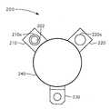
- FIG. 2shows a simplified illustration of a two chamber etch system 200 for etching a high-k flash memory stack.
- a first chamber 210an etch is performed with a cathode 210 c at a temperature below about 100 degrees Celsius to define a control gate 120 from a poly 2 layer or other conducting layer. The etch is stopped at the high-k dielectric material.
- the first chamber 210may be a DPSII etch chamber available from Applied Materials, Inc.
- the wafer 202is transported through a vacuum transport chamber 240 , which typically has a wafer transport means such as a robotic arm (not shown), to a second chamber 220 , where a high-k dielectric etch is performed.
- This processis typically controlled by a microprocessor (not shown).
- the high-k dielectric etchis performed using a hot cathode 220 c with a temperature in a range from about 100 degrees Celsius to about 300 degrees Celsius.
- the high-k dielectric etchis performed using a hot cathode 220 c with a temperature in a range from about 250 degrees Celsius to about 300 degrees Celsius.
- the high-k etchdefines the high-k dielectric 130 shown in FIG. 1 .
- the high-k material filmmay be etched with up to 700% over etch.
- a DPSII-HTavailable from Applied Materials, Inc., or other comparable etch chamber may be used to perform the high-k dielectric etch.
- the second etch chamber 220is a reactive ion etch or RIE chamber, which is used to perform an ion bombardment assisted chemical etch of the high-k material. Such an etch may be performed at less than 100 degrees Celsius, if desired.
- a high-k materialsuch as Al 2 O 3 may be etched with a reactant mixture having BCl 3 and a hydrocarbon passivation gas such as C 2 H 4 , with a diluent of He, as disclosed in U.S. patent application Ser. No. 11/208,573, by Wang et al., entitled METHOD FOR ETCHING HIGH DIELECTRIC CONSTANT MATERIALS, filed Aug. 22, 2005, herein incorporated by reference in its entirety.
- a high temperature etch at greater than about 150 degrees Celsiusmay be used with a BCl 3 based chemistry, to provide high selectivity, with a near vertical Al 2 O 3 interface and virtually no control gate poly attack. Thus, a greater than 1.5 to 1 selectivity between the Al 2 O 3 and poly during the Al 2 O 3 etch is possible.
- a high-k materialsuch as hafnium oxide may be etched using 250 degrees Celsius, or higher.
- the wafer 202is returned back to the first chamber 210 to complete etching of the floating gate 140 .
- the etchis stopped on the gate oxide 150 .
- the floating gate 140may be a poly 1 or other conducting material.
- Various embodimentsmay provide one or more advantages in high-k flash memory processing.
- Using a separate chamber for the high-k dielectric etchallows high temperature etching by forming volatile etch byproducts.
- CF 4 , C 2 F 6 , CHF 3 chemistriescan provide high etch selectivity in conventional processing.
- these etchant gasescombine to form non-volatile compounds, such as AlF 3 in the case of Al 3 O 2 high-k dielectric.
- another chemistry that forms volatile etch byproducts, such as Clcould be used to etch the high-k material.
- etching the entire flash memory stack 100 in a single chambercan produce undesirable etch byproducts. For example, etching a high-k film of Al 2 O 3 and a gate electrode film of polysilicon in the same chamber can result in Al and Si based etch byproducts in the chamber.
- a single chamber clean to achieve consistent chamber performance and a high mean wafer between cleaning or MWBC rateis not easy in a single chamber.
- Using different chambers for etching the high-k material and the gate materiallimits the types of byproducts, so improves process consistency and the MWBC rate.
- a separate first chamber 210 for the polysiliconfor example, a standard clean process may be used in the first chamber 210 , and a different clean process may be used for the high-k dielectric byproducts in the second chamber 220 , depending on the particular byproduct.
- the high temperature for the high-k dielectric plasma etch in the second chamber 220allows the high-k dielectric material to be etched faster than in a conventional low temperature plasma chamber. Further, at high temperature, the etch byproduct is more volatile, without causing much change in the etch rate of polysilicon. Thus, the selectivity to polysilicon is high, allowing use of an over etch of the high-k material of up to about 700%, or even greater than about 700%.
- etching of flash memoryAlthough shown with one chamber 210 for gate etching and one chamber 220 for high-k dielectric etch, in some embodiments additional gate etch chambers and/or high-k dielectric etch chambers may be used. Further, although the above description is made with reference to etching of flash memory, embodiments and implementations of the present invention are applicable to processing of any multilayer stack including high-k dielectric material, and where both low and high temperature plasma etch processes are desirable, or where a low temperature plasma etch combined with a reactive ion etch is beneficial.
Landscapes
- Engineering & Computer Science (AREA)
- Chemical & Material Sciences (AREA)
- Physics & Mathematics (AREA)
- Condensed Matter Physics & Semiconductors (AREA)
- Chemical Kinetics & Catalysis (AREA)
- General Chemical & Material Sciences (AREA)
- General Physics & Mathematics (AREA)
- Manufacturing & Machinery (AREA)
- Computer Hardware Design (AREA)
- Microelectronics & Electronic Packaging (AREA)
- Power Engineering (AREA)
- Plasma & Fusion (AREA)
- Inorganic Chemistry (AREA)
- Semiconductor Memories (AREA)
- Non-Volatile Memory (AREA)
Abstract
Description
- Integrated circuits (IC) play a significant role in the field of modern semiconductor technology. The development of integrated circuits has made possible a modern world with advanced electrical technology. Applications of integrated circuits are so widespread and their significance affects our every day lives from cellular phones, digital televisions, to flash memory chips in cameras. These integrated circuits typically are formed on silicon substrates or wafers, which can include active semiconductor devices with structured processes for a wide range of stacked layers made from different materials, allowing for memory capabilities.
- Recently, in modern semiconductor technology, integrated circuits have advanced towards smaller devices with more memory. In the manufacture of semiconductor integrated circuits (IC), typically, dielectric materials such as silicon dioxide (SiO2), silicon nitride (Si3N4) and silicon oxynitride (SiON) have been widely used. However, as technology has progressed, IC device geometry has become smaller, resulting in progressively thinner integrated circuit devices. When typical IC devices approach thicknesses of a few nanometers or less, conventional aforementioned dielectric materials can typically undergo electronic breakdown and can no longer provide the memory storage needed.
- To address the aforementioned problems, high dielectric constant materials (high k dielectric materials) have been used in semiconductor chip manufacturing with their potential application in memory devices, such as flash memory. A conventional flash memory film stack consists of poly 2 (control gate)/ONO (interpoly dielectric)/poly 1 (floating gate) gate oxide. One of the key changes in the gate film stack at 65 nanometer node and beyond, for flash memory applications, is the replacement of the ONO inter-poly dielectric film with a high-k material. Examples of high-k materials include aluminum oxide, (Al2O3), hafnium oxide (HfOx), zirconium oxide (ZrOx), titanium oxide (TiOx), and mixtures thereof, and metal silicates such as HfSixOy, ZrSiO4and mixtures thereof.
- Because of the different composition and reduced size of the high-k dielectric flash memory stack, processing can not be efficiently carried out with conventional etch chamber processing. Therefore, what is needed is an etch chamber and processing methods designed for efficient processing of high-k dielectric flash memory stacks.
- In one implementation, a method is provided for multi-chamber plasma etching to form high-k dielectric flash memory devices on a wafer. The method includes etching an upper conductive material layer in a first plasma chamber with a cathode temperature below about 100 degrees Celsius to define a control gate and transferring the wafer from the first chamber to a hot cathode chamber without breaking vacuum. In the hot cathode chamber, plasma etching is performed of a high-k dielectric layer with a temperature between about 100 and about 300 degrees Celsius. The wafer is transferred from the hot cathode chamber to the first plasma chamber without breaking vacuum. In the first plasma chamber a lower polysilicon layer is etched with a cathode temperature below about 100 degrees Celsius to define a floating gate electrode.
- In one implementation, a method for etching a wafer to form high-k dielectric flash memory devices is provided. The method includes etching an upper conductor layer in a first plasma chamber to define a control gate. The wafer is transferred from the first plasma chamber to a reactive ion etch chamber without breaking vacuum. A high-k dielectric layer is etched with a reactive ion etch process, and the wafer is transferred back to the first plasma chamber without breaking vacuum. In the first plasma chamber, a lower polysilicon layer is etched to define a floating gate electrode.
- In one implementation a method is provided capable of etching a wafer to form devices including a high-k dielectric layer. The method includes etching an upper conductive material layer in a first plasma chamber with a low cathode temperature and transferring the wafer from the first plasma chamber to a second chamber without breaking vacuum. The high-k dielectric layer is etched in the second chamber. After etching the high-k dielectric layer, the wafer is transferred from the second chamber to the first plasma chamber without breaking vacuum. In the first plasma chamber a lower conductive material layer is etched with a low cathode temperature. In one implementation, the high-k dielectric etch is performed with a plasma using a high temperature cathode. In another implementation, the high-k dielectric etch is performed with a reactive ion etch.
- In one embodiment, an integrated etch station is provided for etching of a flash memory high-k gate stack having a control gate and a floating gate, with a high-k dielectric between them. The integrated etch chamber includes a first plasma chamber capable of etching to define the control gate and the floating gate of the flash memory stack. The first plasma chamber is configured to etch in a temperature range of less than about 100 degrees Celsius. A second chamber is configured to etch the high-k dielectric. A vacuum transfer chamber is coupled between the first plasma chamber and the second chamber, the vacuum transfer chamber includes a wafer transport means for transporting wafers between the first plasma chamber and the second chamber. In some embodiments, the second chamber is a high temperature plasma etch chamber configured to etch in a temperature range of from about 100 degrees Celsius to about 300 degrees Celsius. In other embodiments, the second chamber is a reactive ion etch chamber configured to etch the high-k dielectric.
FIG. 1 shows a simplified example of an etched flash memory stack on a substrate.FIG. 2 shows a simplified illustration of a two chamber etch system for etching a high-k flash memory stack.FIG. 1 shows a simplified example of an etchedflash memory stack 100 on asubstrate 160. Ahardmask 110 in an etch process to define thestack 100. A high-k dielectric130 is located between acontrol gate 120 and afloating gate 140. Thecontrol gate 120 and thefloating gate 140 may be etched from polysilicon layers, or layers of other conducting material (not shown). The high-k dielectric130 is defined from a layer (not shown) of high-k dielectric material after thecontrol gate 120 is defined. Agate oxide 150 is between thefloating gate 140 and thesubstrate 160. Thestack 100 may include additional layers, not shown, such as barrier layers, etch stop layers, or the like.- A conventional ONO-based flash memory gate stack is etched in a chamber like a DPSII poly etcher, manufactured by Applied Materials, Inc., of Santa Clara, Calif., at temperatures between 40-85 degrees Celsius. The temperature requirement primarily is driven by need to etch polysilicon with tight profile and critical dimension control.
- Unlike ONO (SiO2/SiN/SiO2sandwich) films, high-k material films such as Al2O3and HfOx, for example, are very difficult to etch at temperatures below 100 degrees Celsius because the etch byproducts are non-volatile. Hence it is not practical to carry out the complete gate etch for high-k based flash memory stacks100 in a single low temperature chamber.
FIG. 2 shows a simplified illustration of a twochamber etch system 200 for etching a high-k flash memory stack. Referring toFIGS. 1 and 2 , in afirst chamber 210 an etch is performed with acathode 210cat a temperature below about 100 degrees Celsius to define acontrol gate 120 from a poly 2 layer or other conducting layer. The etch is stopped at the high-k dielectric material. Thefirst chamber 210 may be a DPSII etch chamber available from Applied Materials, Inc.- The
wafer 202 is transported through avacuum transport chamber 240, which typically has a wafer transport means such as a robotic arm (not shown), to asecond chamber 220, where a high-k dielectric etch is performed. This process is typically controlled by a microprocessor (not shown). In thesecond chamber 220 the high-k dielectric etch is performed using ahot cathode 220cwith a temperature in a range from about 100 degrees Celsius to about 300 degrees Celsius. In some implementations, the high-k dielectric etch is performed using ahot cathode 220cwith a temperature in a range from about 250 degrees Celsius to about 300 degrees Celsius. The high-k etch defines the high-k dielectric130 shown inFIG. 1 . In thesecond etch chamber 220, the high-k material film may be etched with up to 700% over etch. A DPSII-HT, available from Applied Materials, Inc., or other comparable etch chamber may be used to perform the high-k dielectric etch. - In another embodiment, the
second etch chamber 220 is a reactive ion etch or RIE chamber, which is used to perform an ion bombardment assisted chemical etch of the high-k material. Such an etch may be performed at less than 100 degrees Celsius, if desired. - In one example implementation, a high-k material such as Al2O3may be etched with a reactant mixture having BCl3and a hydrocarbon passivation gas such as C2H4, with a diluent of He, as disclosed in U.S. patent application Ser. No. 11/208,573, by Wang et al., entitled METHOD FOR ETCHING HIGH DIELECTRIC CONSTANT MATERIALS, filed Aug. 22, 2005, herein incorporated by reference in its entirety. In one implementation, a high temperature etch at greater than about 150 degrees Celsius may be used with a BCl3based chemistry, to provide high selectivity, with a near vertical Al2O3interface and virtually no control gate poly attack. Thus, a greater than 1.5 to 1 selectivity between the Al2O3and poly during the Al2O3etch is possible. In another example, a high-k material such as hafnium oxide may be etched using 250 degrees Celsius, or higher.
- After etching the high-
k dielectric 130, thewafer 202 is returned back to thefirst chamber 210 to complete etching of the floatinggate 140. The etch is stopped on thegate oxide 150. The floatinggate 140 may be a poly 1 or other conducting material. - Various embodiments may provide one or more advantages in high-k flash memory processing. Using a separate chamber for the high-k dielectric etch allows high temperature etching by forming volatile etch byproducts. For example, CF4, C2F6, CHF3chemistries can provide high etch selectivity in conventional processing. When used to etch high-k materials, these etchant gases combine to form non-volatile compounds, such as AlF3in the case of Al3O2high-k dielectric. Thus, another chemistry that forms volatile etch byproducts, such as Cl, could be used to etch the high-k material.
- Further, by using separate chambers for the control and/or floating
gate k dielectric 130, it is easier to maintain consistent chamber conditions and wall effects from wafer to wafer, enabling volume production. Moreover, using separate chambers for the etching of flash memory stacks allows different plasma generation sources for the two chambers, one optimized for etching gate materials and the other for etching high-k dielectric materials. In contrast, etching the entireflash memory stack 100 in a single chamber can produce undesirable etch byproducts. For example, etching a high-k film of Al2O3and a gate electrode film of polysilicon in the same chamber can result in Al and Si based etch byproducts in the chamber. Keeping a single chamber clean to achieve consistent chamber performance and a high mean wafer between cleaning or MWBC rate is not easy in a single chamber. Using different chambers for etching the high-k material and the gate material limits the types of byproducts, so improves process consistency and the MWBC rate. By using a separatefirst chamber 210 for the polysilicon for example, a standard clean process may be used in thefirst chamber 210, and a different clean process may be used for the high-k dielectric byproducts in thesecond chamber 220, depending on the particular byproduct. - The high temperature for the high-k dielectric plasma etch in the
second chamber 220, about 100 to about 300 degrees Celsius, allows the high-k dielectric material to be etched faster than in a conventional low temperature plasma chamber. Further, at high temperature, the etch byproduct is more volatile, without causing much change in the etch rate of polysilicon. Thus, the selectivity to polysilicon is high, allowing use of an over etch of the high-k material of up to about 700%, or even greater than about 700%. - Although shown with one
chamber 210 for gate etching and onechamber 220 for high-k dielectric etch, in some embodiments additional gate etch chambers and/or high-k dielectric etch chambers may be used. Further, although the above description is made with reference to etching of flash memory, embodiments and implementations of the present invention are applicable to processing of any multilayer stack including high-k dielectric material, and where both low and high temperature plasma etch processes are desirable, or where a low temperature plasma etch combined with a reactive ion etch is beneficial. - While the invention herein disclosed has been described by the specific embodiments and implementations, numerous modifications and variations could be made thereto by those skilled in the art without departing from the scope of the invention set forth in the claims.
Claims (22)
Priority Applications (4)
| Application Number | Priority Date | Filing Date | Title |
|---|---|---|---|
| US11/386,054US7780862B2 (en) | 2006-03-21 | 2006-03-21 | Device and method for etching flash memory gate stacks comprising high-k dielectric |
| TW096109780ATWI374518B (en) | 2006-03-21 | 2007-03-21 | Device and method for etching flash memory gate stacks comprising high-k dielectric |
| PCT/US2007/007174WO2007109356A2 (en) | 2006-03-21 | 2007-03-21 | Device and method for etching flash memory gate stacks comprising high-k dielectric |
| US11/777,714US20080011423A1 (en) | 2006-03-21 | 2007-07-13 | Device and method for etching flash memory gate stacks comprising high-k dielectric |
Applications Claiming Priority (1)
| Application Number | Priority Date | Filing Date | Title |
|---|---|---|---|
| US11/386,054US7780862B2 (en) | 2006-03-21 | 2006-03-21 | Device and method for etching flash memory gate stacks comprising high-k dielectric |
Related Child Applications (1)
| Application Number | Title | Priority Date | Filing Date |
|---|---|---|---|
| US11/777,714ContinuationUS20080011423A1 (en) | 2006-03-21 | 2007-07-13 | Device and method for etching flash memory gate stacks comprising high-k dielectric |
Publications (2)
| Publication Number | Publication Date |
|---|---|
| US20070224813A1true US20070224813A1 (en) | 2007-09-27 |
| US7780862B2 US7780862B2 (en) | 2010-08-24 |
Family
ID=38523111
Family Applications (2)
| Application Number | Title | Priority Date | Filing Date |
|---|---|---|---|
| US11/386,054Expired - Fee RelatedUS7780862B2 (en) | 2006-03-21 | 2006-03-21 | Device and method for etching flash memory gate stacks comprising high-k dielectric |
| US11/777,714AbandonedUS20080011423A1 (en) | 2006-03-21 | 2007-07-13 | Device and method for etching flash memory gate stacks comprising high-k dielectric |
Family Applications After (1)
| Application Number | Title | Priority Date | Filing Date |
|---|---|---|---|
| US11/777,714AbandonedUS20080011423A1 (en) | 2006-03-21 | 2007-07-13 | Device and method for etching flash memory gate stacks comprising high-k dielectric |
Country Status (3)
| Country | Link |
|---|---|
| US (2) | US7780862B2 (en) |
| TW (1) | TWI374518B (en) |
| WO (1) | WO2007109356A2 (en) |
Cited By (11)
| Publication number | Priority date | Publication date | Assignee | Title |
|---|---|---|---|---|
| EP2009681A2 (en) | 2007-06-27 | 2008-12-31 | Applied Materials, Inc. | Methods for high temperature etching a high-k material gate structure |
| US20090155967A1 (en)* | 2007-12-18 | 2009-06-18 | Vinod Robert Purayath | Method of forming memory with floating gates including self-aligned metal nanodots using a coupling layer |
| US20090189280A1 (en)* | 2008-01-30 | 2009-07-30 | Daniel Pak-Chum Shum | Method of Forming a Non Volatile Memory Device |
| US20090195994A1 (en)* | 2008-01-31 | 2009-08-06 | Macdonald Alexander S | Access self-service terminal |
| US20110020992A1 (en)* | 2009-07-21 | 2011-01-27 | Vinod Robert Purayath | Integrated Nanostructure-Based Non-Volatile Memory Fabrication |
| US8193055B1 (en) | 2007-12-18 | 2012-06-05 | Sandisk Technologies Inc. | Method of forming memory with floating gates including self-aligned metal nanodots using a polymer solution |
| US9401663B2 (en) | 2012-12-21 | 2016-07-26 | Infineon Technologies Austria Ag | Power converter circuit with AC output |
| US9425622B2 (en) | 2013-01-08 | 2016-08-23 | Infineon Technologies Austria Ag | Power converter circuit with AC output and at least one transformer |
| US9461474B2 (en) | 2012-01-17 | 2016-10-04 | Infineon Technologies Austria Ag | Power converter circuit with AC output |
| US9478989B2 (en) | 2012-01-17 | 2016-10-25 | Infineon Technologies Austria Ag | Power converter circuit with AC output |
| US9484746B2 (en) | 2012-01-17 | 2016-11-01 | Infineon Technologies Austria Ag | Power converter circuit with AC output |
Families Citing this family (3)
| Publication number | Priority date | Publication date | Assignee | Title |
|---|---|---|---|---|
| US8722547B2 (en)* | 2006-04-20 | 2014-05-13 | Applied Materials, Inc. | Etching high K dielectrics with high selectivity to oxide containing layers at elevated temperatures with BC13 based etch chemistries |
| US8804457B2 (en) | 2011-03-31 | 2014-08-12 | Maxim Integrated Products, Inc. | Transmit/receive systems for imaging devices |
| JP6173684B2 (en)* | 2012-12-25 | 2017-08-02 | 株式会社日立ハイテクノロジーズ | Manufacturing method of semiconductor device |
Citations (73)
| Publication number | Priority date | Publication date | Assignee | Title |
|---|---|---|---|---|
| US4372807A (en)* | 1982-03-25 | 1983-02-08 | Rca Corporation | Plasma etching of aluminum |
| US4375385A (en)* | 1982-03-25 | 1983-03-01 | Rca Corporation | Plasma etching of aluminum |
| US4482419A (en)* | 1983-02-03 | 1984-11-13 | Anelva Corporation | Dry etching apparatus comprising etching chambers of different etching rate distributions |
| US4563240A (en)* | 1983-08-10 | 1986-01-07 | Hitachi, Ltd. | Method and apparatus for plasma process |
| US4618398A (en)* | 1984-02-13 | 1986-10-21 | Hitachi, Ltd. | Dry etching method |
| US4680086A (en)* | 1986-03-20 | 1987-07-14 | Motorola, Inc. | Dry etching of multi-layer structures |
| US4842676A (en)* | 1987-07-16 | 1989-06-27 | Texas Instruments Incorporated | Process for etch of tungsten |
| US4855016A (en)* | 1987-07-16 | 1989-08-08 | Texas Instruments Incorporated | Method for etching aluminum film doped with copper |
| US4897154A (en)* | 1986-07-03 | 1990-01-30 | International Business Machines Corporation | Post dry-etch cleaning method for restoring wafer properties |
| US4940509A (en)* | 1988-03-25 | 1990-07-10 | Texas Instruments, Incorporated | Isotropic etchant for capped silicide processes |
| US5223453A (en)* | 1991-03-19 | 1993-06-29 | The United States Of America As Represented By The United States Department Of Energy | Controlled metal-semiconductor sintering/alloying by one-directional reverse illumination |
| US5236537A (en)* | 1989-04-07 | 1993-08-17 | Seiko Epson Corporation | Plasma etching apparatus |
| US5252181A (en)* | 1990-12-20 | 1993-10-12 | Etablissement Autonome De Droit Public: France Telecom | Method for cleaning the surface of a substrate with plasma |
| US5258333A (en)* | 1992-08-18 | 1993-11-02 | Intel Corporation | Composite dielectric for a semiconductor device and method of fabrication |
| US5427638A (en)* | 1992-06-04 | 1995-06-27 | Alliedsignal Inc. | Low temperature reaction bonding |
| US5462635A (en)* | 1991-01-29 | 1995-10-31 | Hitachi, Ltd. | Surface processing method and an apparatus for carrying out the same |
| US5466636A (en)* | 1992-09-17 | 1995-11-14 | International Business Machines Corporation | Method of forming borderless contacts using a removable mandrel |
| US5468679A (en)* | 1991-02-25 | 1995-11-21 | Symetrix Corporation | Process for fabricating materials for ferroelectric, high dielectric constant, and integrated circuit applications |
| US5470797A (en)* | 1993-04-05 | 1995-11-28 | Ford Motor Company | Method for producing a silicon-on-insulator capacitive surface micromachined absolute pressure sensor |
| US5578133A (en)* | 1992-01-13 | 1996-11-26 | Fujitsu Limited | Dry cleaning process for cleaning a surface |
| US5769952A (en)* | 1994-06-07 | 1998-06-23 | Tokyo Electron, Ltd. | Reduced pressure and normal pressure treatment apparatus |
| US5786277A (en)* | 1995-09-29 | 1998-07-28 | Nec Corporation | Method of manufacturing a semiconductor device having an oxide film of a high quality on a semiconductor substrate |
| US5895248A (en)* | 1995-10-20 | 1999-04-20 | U.S. Philips Corporation | Manufacture of a semiconductor device with selectively deposited semiconductor zone |
| US5933751A (en)* | 1997-01-23 | 1999-08-03 | Sumitomo Electric Industries Ltd. | Method for the heat treatment of II-VI semiconductors |
| US5932048A (en)* | 1995-04-06 | 1999-08-03 | Komatsu Electronic Metals Co., Ltd. | Method of fabricating direct-bonded semiconductor wafers |
| US5968848A (en)* | 1996-12-27 | 1999-10-19 | Tokyo Ohka Kogyo Co., Ltd. | Process for treating a lithographic substrate and a rinse solution for the treatment |
| US5983907A (en)* | 1997-08-05 | 1999-11-16 | Seh America, Inc. | Method of drying semiconductor wafers using hot deionized water and infrared drying |
| US6010966A (en)* | 1998-08-07 | 2000-01-04 | Applied Materials, Inc. | Hydrocarbon gases for anisotropic etching of metal-containing layers |
| US6077776A (en)* | 1998-03-18 | 2000-06-20 | Taiwan Semiconductor Manufacturing Company | Polysilicon residue free process by thermal treatment |
| US6090717A (en)* | 1996-03-26 | 2000-07-18 | Lam Research Corporation | High density plasma etching of metallization layer using chlorine and nitrogen |
| US6107192A (en)* | 1997-12-30 | 2000-08-22 | Applied Materials, Inc. | Reactive preclean prior to metallization for sub-quarter micron application |
| US6146929A (en)* | 1998-07-09 | 2000-11-14 | Kabushiki Kaisha Toshiba | Method for manufacturing semiconductor device using multiple steps continuously without exposing substrate to the atmosphere |
| US6180505B1 (en)* | 1999-01-07 | 2001-01-30 | International Business Machines Corporation | Process for forming a copper-containing film |
| US6204087B1 (en)* | 1997-02-07 | 2001-03-20 | University Of Hawai'i | Fabrication of three-dimensional architecture for solid state radiation detectors |
| US6255226B1 (en)* | 1998-12-01 | 2001-07-03 | Philips Semiconductor, Inc. | Optimized metal etch process to enable the use of aluminum plugs |
| US6265749B1 (en)* | 1997-10-14 | 2001-07-24 | Advanced Micro Devices, Inc. | Metal silicide transistor gate spaced from a semiconductor substrate by a ceramic gate dielectric having a high dielectric constant |
| US6277767B1 (en)* | 1999-04-06 | 2001-08-21 | Nec Corporation | Method for cleaning semiconductor device |
| US6303505B1 (en)* | 1998-07-09 | 2001-10-16 | Advanced Micro Devices, Inc. | Copper interconnect with improved electromigration resistance |
| US20010046738A1 (en)* | 1999-03-05 | 2001-11-29 | Kenneth Wo-Wai Au | Method of forming high k tantalum pentoxide ta205 instead of ono stacked films to increase coupling ratio and improve reliability for flash memory devices |
| US6329276B1 (en)* | 1998-12-01 | 2001-12-11 | Samsung Electronics Co. Ltd. | Method of forming self-aligned silicide in semiconductor device |
| US20020005392A1 (en)* | 1997-11-17 | 2002-01-17 | Leroy Luo | Systems and methods for variable mode plasma enhanced processing of semiconductor wafers |
| US6413863B1 (en)* | 2000-01-24 | 2002-07-02 | Taiwan Semiconductor Manufacturing Company | Method to resolve the passivation surface roughness during formation of the AlCu pad for the copper process |
| US20020119669A1 (en)* | 2001-02-23 | 2002-08-29 | Nec Corporation | Method of fabricating semiconductor device |
| US6451647B1 (en)* | 2002-03-18 | 2002-09-17 | Advanced Micro Devices, Inc. | Integrated plasma etch of gate and gate dielectric and low power plasma post gate etch removal of high-K residual |
| US6500357B1 (en)* | 1999-12-28 | 2002-12-31 | Applied Materials Inc. | System level in-situ integrated dielectric etch process particularly useful for copper dual damascene |
| US6508920B1 (en)* | 1998-02-04 | 2003-01-21 | Semitool, Inc. | Apparatus for low-temperature annealing of metallization microstructures in the production of a microelectronic device |
| US6511918B2 (en)* | 1998-12-04 | 2003-01-28 | Infineon Technologies Ag | Method of structuring a metal-containing layer |
| US6511872B1 (en)* | 2001-07-10 | 2003-01-28 | Agere Systems Inc. | Device having a high dielectric constant material and a method of manufacture thereof |
| US20030045098A1 (en)* | 2001-08-31 | 2003-03-06 | Applied Materials, Inc. | Method and apparatus for processing a wafer |
| US20030067023A1 (en)* | 2001-10-09 | 2003-04-10 | Koninklijke Philips Electronics N.V. | Metal-insulator-metal (MIM) capacitor structure and methods of fabricating same |
| US6566148B2 (en)* | 2001-08-13 | 2003-05-20 | Sharp Laboratories Of America, Inc. | Method of making a ferroelectric memory transistor |
| US6566211B2 (en)* | 1997-06-11 | 2003-05-20 | Texas Instruments Incorporated | Surface modified interconnects |
| US20030129847A1 (en)* | 2001-12-31 | 2003-07-10 | Celii Francis G. | FeRAM sidewall diffusion barrier etch |
| US20030170985A1 (en)* | 2002-03-06 | 2003-09-11 | Applied Materials, Inc. | Etching methods for a magnetic memory cell stack |
| US20030194877A1 (en)* | 2002-04-16 | 2003-10-16 | Applied Materials, Inc. | Integrated etch, rinse and dry, and anneal method and system |
| US6660647B1 (en)* | 1998-03-12 | 2003-12-09 | Hitachi, Ltd. | Method for processing surface of sample |
| US6666986B1 (en)* | 1997-05-05 | 2003-12-23 | Micron Technology, Inc. | Supercritical etching compositions and method of using same |
| US20040007561A1 (en)* | 2002-07-12 | 2004-01-15 | Applied Materials, Inc. | Method for plasma etching of high-K dielectric materials |
| US20040011380A1 (en)* | 2002-07-18 | 2004-01-22 | Bing Ji | Method for etching high dielectric constant materials and for cleaning deposition chambers for high dielectric constant materials |
| US20040074869A1 (en)* | 2002-10-18 | 2004-04-22 | Applied Materials, Inc. | Fluorine free integrated process for etching aluminum including chamber dry clean |
| US20040262262A1 (en)* | 2003-06-27 | 2004-12-30 | Hsien-Kuang Chiu | Process for patterning high-k dielectric material |
| US20050081781A1 (en)* | 2003-10-17 | 2005-04-21 | Taiwan Semiconductor Manufacturing Co. | Fully dry, Si recess free process for removing high k dielectric layer |
| US20050118353A1 (en)* | 2003-05-30 | 2005-06-02 | Tokyo Electron Limited | Method and system for etching a high-k dielectric material |
| US20050153563A1 (en)* | 2004-01-14 | 2005-07-14 | Lam Research Corporation | Selective etch of films with high dielectric constant |
| US20050164479A1 (en)* | 2004-01-27 | 2005-07-28 | Taiwan Semiconductor Manufacturing Co. | Zirconium oxide and hafnium oxide etching using halogen containing chemicals |
| US20050176191A1 (en)* | 2003-02-04 | 2005-08-11 | Applied Materials, Inc. | Method for fabricating a notched gate structure of a field effect transistor |
| US20050215062A1 (en)* | 2004-03-16 | 2005-09-29 | Osamu Miyagawa | Method of manufacturing semiconductor device |
| US20050282341A1 (en)* | 2004-06-16 | 2005-12-22 | International Business Machines Corporation | High-temperature stable gate structure with metallic electrode |
| US20070042601A1 (en)* | 2005-08-22 | 2007-02-22 | Applied Materials, Inc. | Method for etching high dielectric constant materials |
| US20070190795A1 (en)* | 2006-02-13 | 2007-08-16 | Haoren Zhuang | Method for fabricating a semiconductor device with a high-K dielectric |
| US20070231986A1 (en)* | 2006-03-28 | 2007-10-04 | Hynix Semiconductor, Inc. | Method of manufacturing flash memory device |
| US20070238302A1 (en)* | 2006-03-31 | 2007-10-11 | Tokyo Electron Limited | Sequential oxide removal using fluorine and hydrogen |
| US20070249182A1 (en)* | 2006-04-20 | 2007-10-25 | Applied Materials, Inc. | ETCHING OF SiO2 WITH HIGH SELECTIVITY TO Si3N4 AND ETCHING METAL OXIDES WITH HIGH SELECTIVITY TO SiO2 AT ELEVATED TEMPERATURES WITH BCl3 BASED ETCH CHEMISTRIES |
Family Cites Families (4)
| Publication number | Priority date | Publication date | Assignee | Title |
|---|---|---|---|---|
| JPH02291131A (en) | 1989-04-28 | 1990-11-30 | Sony Corp | Dry etching of barrier metal/aluminum laminated film |
| JP2560178B2 (en) | 1992-06-29 | 1996-12-04 | 九州電子金属株式会社 | Method for manufacturing semiconductor wafer |
| JP3115715B2 (en) | 1992-11-12 | 2000-12-11 | 三菱電機株式会社 | Method for etching multi-component oxide film having high dielectric constant, method for etching high-melting-point metal-containing film, and method for manufacturing thin-film capacitor element |
| JP4358556B2 (en) | 2003-05-30 | 2009-11-04 | 富士通マイクロエレクトロニクス株式会社 | Manufacturing method of semiconductor device |
- 2006
- 2006-03-21USUS11/386,054patent/US7780862B2/ennot_activeExpired - Fee Related
- 2007
- 2007-03-21WOPCT/US2007/007174patent/WO2007109356A2/enactiveApplication Filing
- 2007-03-21TWTW096109780Apatent/TWI374518B/ennot_activeIP Right Cessation
- 2007-07-13USUS11/777,714patent/US20080011423A1/ennot_activeAbandoned
Patent Citations (74)
| Publication number | Priority date | Publication date | Assignee | Title |
|---|---|---|---|---|
| US4372807A (en)* | 1982-03-25 | 1983-02-08 | Rca Corporation | Plasma etching of aluminum |
| US4375385A (en)* | 1982-03-25 | 1983-03-01 | Rca Corporation | Plasma etching of aluminum |
| US4482419A (en)* | 1983-02-03 | 1984-11-13 | Anelva Corporation | Dry etching apparatus comprising etching chambers of different etching rate distributions |
| US4563240A (en)* | 1983-08-10 | 1986-01-07 | Hitachi, Ltd. | Method and apparatus for plasma process |
| US4618398A (en)* | 1984-02-13 | 1986-10-21 | Hitachi, Ltd. | Dry etching method |
| US4680086A (en)* | 1986-03-20 | 1987-07-14 | Motorola, Inc. | Dry etching of multi-layer structures |
| US4897154A (en)* | 1986-07-03 | 1990-01-30 | International Business Machines Corporation | Post dry-etch cleaning method for restoring wafer properties |
| US4855016A (en)* | 1987-07-16 | 1989-08-08 | Texas Instruments Incorporated | Method for etching aluminum film doped with copper |
| US4842676A (en)* | 1987-07-16 | 1989-06-27 | Texas Instruments Incorporated | Process for etch of tungsten |
| US4940509A (en)* | 1988-03-25 | 1990-07-10 | Texas Instruments, Incorporated | Isotropic etchant for capped silicide processes |
| US5236537A (en)* | 1989-04-07 | 1993-08-17 | Seiko Epson Corporation | Plasma etching apparatus |
| US5252181A (en)* | 1990-12-20 | 1993-10-12 | Etablissement Autonome De Droit Public: France Telecom | Method for cleaning the surface of a substrate with plasma |
| US5462635A (en)* | 1991-01-29 | 1995-10-31 | Hitachi, Ltd. | Surface processing method and an apparatus for carrying out the same |
| US5468679A (en)* | 1991-02-25 | 1995-11-21 | Symetrix Corporation | Process for fabricating materials for ferroelectric, high dielectric constant, and integrated circuit applications |
| US5223453A (en)* | 1991-03-19 | 1993-06-29 | The United States Of America As Represented By The United States Department Of Energy | Controlled metal-semiconductor sintering/alloying by one-directional reverse illumination |
| US5578133A (en)* | 1992-01-13 | 1996-11-26 | Fujitsu Limited | Dry cleaning process for cleaning a surface |
| US5427638A (en)* | 1992-06-04 | 1995-06-27 | Alliedsignal Inc. | Low temperature reaction bonding |
| US5258333A (en)* | 1992-08-18 | 1993-11-02 | Intel Corporation | Composite dielectric for a semiconductor device and method of fabrication |
| US5466636A (en)* | 1992-09-17 | 1995-11-14 | International Business Machines Corporation | Method of forming borderless contacts using a removable mandrel |
| US5470797A (en)* | 1993-04-05 | 1995-11-28 | Ford Motor Company | Method for producing a silicon-on-insulator capacitive surface micromachined absolute pressure sensor |
| US5769952A (en)* | 1994-06-07 | 1998-06-23 | Tokyo Electron, Ltd. | Reduced pressure and normal pressure treatment apparatus |
| US5932048A (en)* | 1995-04-06 | 1999-08-03 | Komatsu Electronic Metals Co., Ltd. | Method of fabricating direct-bonded semiconductor wafers |
| US5786277A (en)* | 1995-09-29 | 1998-07-28 | Nec Corporation | Method of manufacturing a semiconductor device having an oxide film of a high quality on a semiconductor substrate |
| US5895248A (en)* | 1995-10-20 | 1999-04-20 | U.S. Philips Corporation | Manufacture of a semiconductor device with selectively deposited semiconductor zone |
| US6090717A (en)* | 1996-03-26 | 2000-07-18 | Lam Research Corporation | High density plasma etching of metallization layer using chlorine and nitrogen |
| US5968848A (en)* | 1996-12-27 | 1999-10-19 | Tokyo Ohka Kogyo Co., Ltd. | Process for treating a lithographic substrate and a rinse solution for the treatment |
| US5933751A (en)* | 1997-01-23 | 1999-08-03 | Sumitomo Electric Industries Ltd. | Method for the heat treatment of II-VI semiconductors |
| US6204087B1 (en)* | 1997-02-07 | 2001-03-20 | University Of Hawai'i | Fabrication of three-dimensional architecture for solid state radiation detectors |
| US6666986B1 (en)* | 1997-05-05 | 2003-12-23 | Micron Technology, Inc. | Supercritical etching compositions and method of using same |
| US6566211B2 (en)* | 1997-06-11 | 2003-05-20 | Texas Instruments Incorporated | Surface modified interconnects |
| US5983907A (en)* | 1997-08-05 | 1999-11-16 | Seh America, Inc. | Method of drying semiconductor wafers using hot deionized water and infrared drying |
| US6265749B1 (en)* | 1997-10-14 | 2001-07-24 | Advanced Micro Devices, Inc. | Metal silicide transistor gate spaced from a semiconductor substrate by a ceramic gate dielectric having a high dielectric constant |
| US20020005392A1 (en)* | 1997-11-17 | 2002-01-17 | Leroy Luo | Systems and methods for variable mode plasma enhanced processing of semiconductor wafers |
| US6107192A (en)* | 1997-12-30 | 2000-08-22 | Applied Materials, Inc. | Reactive preclean prior to metallization for sub-quarter micron application |
| US6508920B1 (en)* | 1998-02-04 | 2003-01-21 | Semitool, Inc. | Apparatus for low-temperature annealing of metallization microstructures in the production of a microelectronic device |
| US6660647B1 (en)* | 1998-03-12 | 2003-12-09 | Hitachi, Ltd. | Method for processing surface of sample |
| US6077776A (en)* | 1998-03-18 | 2000-06-20 | Taiwan Semiconductor Manufacturing Company | Polysilicon residue free process by thermal treatment |
| US6303505B1 (en)* | 1998-07-09 | 2001-10-16 | Advanced Micro Devices, Inc. | Copper interconnect with improved electromigration resistance |
| US6146929A (en)* | 1998-07-09 | 2000-11-14 | Kabushiki Kaisha Toshiba | Method for manufacturing semiconductor device using multiple steps continuously without exposing substrate to the atmosphere |
| US6010966A (en)* | 1998-08-07 | 2000-01-04 | Applied Materials, Inc. | Hydrocarbon gases for anisotropic etching of metal-containing layers |
| US6329276B1 (en)* | 1998-12-01 | 2001-12-11 | Samsung Electronics Co. Ltd. | Method of forming self-aligned silicide in semiconductor device |
| US6255226B1 (en)* | 1998-12-01 | 2001-07-03 | Philips Semiconductor, Inc. | Optimized metal etch process to enable the use of aluminum plugs |
| US6511918B2 (en)* | 1998-12-04 | 2003-01-28 | Infineon Technologies Ag | Method of structuring a metal-containing layer |
| US6180505B1 (en)* | 1999-01-07 | 2001-01-30 | International Business Machines Corporation | Process for forming a copper-containing film |
| US20010046738A1 (en)* | 1999-03-05 | 2001-11-29 | Kenneth Wo-Wai Au | Method of forming high k tantalum pentoxide ta205 instead of ono stacked films to increase coupling ratio and improve reliability for flash memory devices |
| US6277767B1 (en)* | 1999-04-06 | 2001-08-21 | Nec Corporation | Method for cleaning semiconductor device |
| US6500357B1 (en)* | 1999-12-28 | 2002-12-31 | Applied Materials Inc. | System level in-situ integrated dielectric etch process particularly useful for copper dual damascene |
| US6413863B1 (en)* | 2000-01-24 | 2002-07-02 | Taiwan Semiconductor Manufacturing Company | Method to resolve the passivation surface roughness during formation of the AlCu pad for the copper process |
| US20020119669A1 (en)* | 2001-02-23 | 2002-08-29 | Nec Corporation | Method of fabricating semiconductor device |
| US6511872B1 (en)* | 2001-07-10 | 2003-01-28 | Agere Systems Inc. | Device having a high dielectric constant material and a method of manufacture thereof |
| US6566148B2 (en)* | 2001-08-13 | 2003-05-20 | Sharp Laboratories Of America, Inc. | Method of making a ferroelectric memory transistor |
| US20030045098A1 (en)* | 2001-08-31 | 2003-03-06 | Applied Materials, Inc. | Method and apparatus for processing a wafer |
| US20030067023A1 (en)* | 2001-10-09 | 2003-04-10 | Koninklijke Philips Electronics N.V. | Metal-insulator-metal (MIM) capacitor structure and methods of fabricating same |
| US20030129847A1 (en)* | 2001-12-31 | 2003-07-10 | Celii Francis G. | FeRAM sidewall diffusion barrier etch |
| US20030170985A1 (en)* | 2002-03-06 | 2003-09-11 | Applied Materials, Inc. | Etching methods for a magnetic memory cell stack |
| US6451647B1 (en)* | 2002-03-18 | 2002-09-17 | Advanced Micro Devices, Inc. | Integrated plasma etch of gate and gate dielectric and low power plasma post gate etch removal of high-K residual |
| US20030194877A1 (en)* | 2002-04-16 | 2003-10-16 | Applied Materials, Inc. | Integrated etch, rinse and dry, and anneal method and system |
| US20040007561A1 (en)* | 2002-07-12 | 2004-01-15 | Applied Materials, Inc. | Method for plasma etching of high-K dielectric materials |
| US20040011380A1 (en)* | 2002-07-18 | 2004-01-22 | Bing Ji | Method for etching high dielectric constant materials and for cleaning deposition chambers for high dielectric constant materials |
| US20040074869A1 (en)* | 2002-10-18 | 2004-04-22 | Applied Materials, Inc. | Fluorine free integrated process for etching aluminum including chamber dry clean |
| US20050176191A1 (en)* | 2003-02-04 | 2005-08-11 | Applied Materials, Inc. | Method for fabricating a notched gate structure of a field effect transistor |
| US20050118353A1 (en)* | 2003-05-30 | 2005-06-02 | Tokyo Electron Limited | Method and system for etching a high-k dielectric material |
| US20050164511A1 (en)* | 2003-05-30 | 2005-07-28 | Tokyo Electron Limited | Method and system for etching a high-k dielectric material |
| US20040262262A1 (en)* | 2003-06-27 | 2004-12-30 | Hsien-Kuang Chiu | Process for patterning high-k dielectric material |
| US20050081781A1 (en)* | 2003-10-17 | 2005-04-21 | Taiwan Semiconductor Manufacturing Co. | Fully dry, Si recess free process for removing high k dielectric layer |
| US20050153563A1 (en)* | 2004-01-14 | 2005-07-14 | Lam Research Corporation | Selective etch of films with high dielectric constant |
| US20050164479A1 (en)* | 2004-01-27 | 2005-07-28 | Taiwan Semiconductor Manufacturing Co. | Zirconium oxide and hafnium oxide etching using halogen containing chemicals |
| US20050215062A1 (en)* | 2004-03-16 | 2005-09-29 | Osamu Miyagawa | Method of manufacturing semiconductor device |
| US20050282341A1 (en)* | 2004-06-16 | 2005-12-22 | International Business Machines Corporation | High-temperature stable gate structure with metallic electrode |
| US20070042601A1 (en)* | 2005-08-22 | 2007-02-22 | Applied Materials, Inc. | Method for etching high dielectric constant materials |
| US20070190795A1 (en)* | 2006-02-13 | 2007-08-16 | Haoren Zhuang | Method for fabricating a semiconductor device with a high-K dielectric |
| US20070231986A1 (en)* | 2006-03-28 | 2007-10-04 | Hynix Semiconductor, Inc. | Method of manufacturing flash memory device |
| US20070238302A1 (en)* | 2006-03-31 | 2007-10-11 | Tokyo Electron Limited | Sequential oxide removal using fluorine and hydrogen |
| US20070249182A1 (en)* | 2006-04-20 | 2007-10-25 | Applied Materials, Inc. | ETCHING OF SiO2 WITH HIGH SELECTIVITY TO Si3N4 AND ETCHING METAL OXIDES WITH HIGH SELECTIVITY TO SiO2 AT ELEVATED TEMPERATURES WITH BCl3 BASED ETCH CHEMISTRIES |
Cited By (18)
| Publication number | Priority date | Publication date | Assignee | Title |
|---|---|---|---|---|
| EP2009681A2 (en) | 2007-06-27 | 2008-12-31 | Applied Materials, Inc. | Methods for high temperature etching a high-k material gate structure |
| US8263465B2 (en) | 2007-12-18 | 2012-09-11 | Sandisk Technologies Inc. | Method of forming memory with floating gates including self-aligned metal nanodots using a coupling layer |
| US7723186B2 (en) | 2007-12-18 | 2010-05-25 | Sandisk Corporation | Method of forming memory with floating gates including self-aligned metal nanodots using a coupling layer |
| US20100190319A1 (en)* | 2007-12-18 | 2010-07-29 | Vinod Robert Purayath | Method of forming memory with floating gates including self-aligned metal nanodots using a coupling layer |
| US8193055B1 (en) | 2007-12-18 | 2012-06-05 | Sandisk Technologies Inc. | Method of forming memory with floating gates including self-aligned metal nanodots using a polymer solution |
| US20090155967A1 (en)* | 2007-12-18 | 2009-06-18 | Vinod Robert Purayath | Method of forming memory with floating gates including self-aligned metal nanodots using a coupling layer |
| US20090189280A1 (en)* | 2008-01-30 | 2009-07-30 | Daniel Pak-Chum Shum | Method of Forming a Non Volatile Memory Device |
| US9418864B2 (en)* | 2008-01-30 | 2016-08-16 | Infineon Technologies Ag | Method of forming a non volatile memory device using wet etching |
| US20090195994A1 (en)* | 2008-01-31 | 2009-08-06 | Macdonald Alexander S | Access self-service terminal |
| US8946022B2 (en) | 2009-07-21 | 2015-02-03 | Sandisk Technologies Inc. | Integrated nanostructure-based non-volatile memory fabrication |
| US8383479B2 (en) | 2009-07-21 | 2013-02-26 | Sandisk Technologies Inc. | Integrated nanostructure-based non-volatile memory fabrication |
| US20110020992A1 (en)* | 2009-07-21 | 2011-01-27 | Vinod Robert Purayath | Integrated Nanostructure-Based Non-Volatile Memory Fabrication |
| US9461474B2 (en) | 2012-01-17 | 2016-10-04 | Infineon Technologies Austria Ag | Power converter circuit with AC output |
| US9478989B2 (en) | 2012-01-17 | 2016-10-25 | Infineon Technologies Austria Ag | Power converter circuit with AC output |
| US9484746B2 (en) | 2012-01-17 | 2016-11-01 | Infineon Technologies Austria Ag | Power converter circuit with AC output |
| US10084317B2 (en) | 2012-01-17 | 2018-09-25 | Infineon Technologies Austria Ag | Power converter circuit with AC output |
| US9401663B2 (en) | 2012-12-21 | 2016-07-26 | Infineon Technologies Austria Ag | Power converter circuit with AC output |
| US9425622B2 (en) | 2013-01-08 | 2016-08-23 | Infineon Technologies Austria Ag | Power converter circuit with AC output and at least one transformer |
Also Published As
| Publication number | Publication date |
|---|---|
| TWI374518B (en) | 2012-10-11 |
| US20080011423A1 (en) | 2008-01-17 |
| US7780862B2 (en) | 2010-08-24 |
| TW200802733A (en) | 2008-01-01 |
| WO2007109356A3 (en) | 2007-12-13 |
| WO2007109356A2 (en) | 2007-09-27 |
Similar Documents
| Publication | Publication Date | Title |
|---|---|---|
| US7780862B2 (en) | Device and method for etching flash memory gate stacks comprising high-k dielectric | |
| US10692880B2 (en) | 3D NAND high aspect ratio structure etch | |
| CN102610515B (en) | Methods for high temperature etching a high-k material gate structure | |
| US6451647B1 (en) | Integrated plasma etch of gate and gate dielectric and low power plasma post gate etch removal of high-K residual | |
| US6764898B1 (en) | Implantation into high-K dielectric material after gate etch to facilitate removal | |
| US7964512B2 (en) | Method for etching high dielectric constant materials | |
| US20070210354A1 (en) | Semiconductor device and semiconductor device manufacturing method | |
| US7579282B2 (en) | Method for removing metal foot during high-k dielectric/metal gate etching | |
| TWI604562B (en) | Selective nitridation method | |
| US10497578B2 (en) | Methods for high temperature etching a material layer using protection coating | |
| US9478643B2 (en) | Memory structure with self-aligned floating and control gates and associated methods | |
| US11127599B2 (en) | Methods for etching a hardmask layer | |
| US7910488B2 (en) | Alternative method for advanced CMOS logic gate etch applications | |
| JP6104928B2 (en) | Interlayer polycrystalline silicon dielectric cap and method of forming the same | |
| TWI647822B (en) | Three-dimensional non-volatile memory and manufacturing method thereof | |
| CN100468635C (en) | Manufacturing method of metal oxide semiconductor device | |
| CN101339903A (en) | Method for high temperature etching of high-K material gate structures | |
| CN100414687C (en) | Manufacturing method of NAND type flash memory device | |
| KR100650799B1 (en) | Manufacturing Method of Flash Memory Device | |
| KR20080046349A (en) | Manufacturing method of nonvolatile semiconductor device | |
| KR20060029383A (en) | Manufacturing method of nonvolatile memory device | |
| KR20070022608A (en) | Etching Method of High Dielectric Constant Material | |
| TW201644082A (en) | Memory device and method for fabricating the same |
Legal Events
| Date | Code | Title | Description |
|---|---|---|---|
| AS | Assignment | Owner name:APPLIED MATERIALS, INC., CALIFORNIA Free format text:ASSIGNMENT OF ASSIGNORS INTEREST;ASSIGNORS:SHEN, MEIHUA;WANG, XIKUN;LIU, WEI;AND OTHERS;SIGNING DATES FROM 19991120 TO 20060622;REEL/FRAME:018990/0192 Owner name:APPLIED MATERIALS, INC., CALIFORNIA Free format text:ASSIGNMENT OF ASSIGNORS INTEREST;ASSIGNORS:SHEN, MEIHUA;WANG, XIKUN;LIU, WEI;AND OTHERS;REEL/FRAME:018990/0192;SIGNING DATES FROM 19991120 TO 20060622 | |
| AS | Assignment | Owner name:APPLIED MATERIALS, INC., CALIFORNIA Free format text:ASSIGNMENT OF ASSIGNORS INTEREST;ASSIGNOR:DU, YAN;REEL/FRAME:019112/0167 Effective date:20070323 | |
| CC | Certificate of correction | ||
| FPAY | Fee payment | Year of fee payment:4 | |
| FEPP | Fee payment procedure | Free format text:MAINTENANCE FEE REMINDER MAILED (ORIGINAL EVENT CODE: REM.) | |
| LAPS | Lapse for failure to pay maintenance fees | Free format text:PATENT EXPIRED FOR FAILURE TO PAY MAINTENANCE FEES (ORIGINAL EVENT CODE: EXP.); ENTITY STATUS OF PATENT OWNER: LARGE ENTITY | |
| STCH | Information on status: patent discontinuation | Free format text:PATENT EXPIRED DUE TO NONPAYMENT OF MAINTENANCE FEES UNDER 37 CFR 1.362 | |
| FP | Lapsed due to failure to pay maintenance fee | Effective date:20180824 |