US20070224772A1 - Method for forming a stressor structure - Google Patents
Method for forming a stressor structureDownload PDFInfo
- Publication number
- US20070224772A1 US20070224772A1US11/386,539US38653906AUS2007224772A1US 20070224772 A1US20070224772 A1US 20070224772A1US 38653906 AUS38653906 AUS 38653906AUS 2007224772 A1US2007224772 A1US 2007224772A1
- Authority
- US
- United States
- Prior art keywords
- layer
- trench
- oxide
- stressor
- semiconductor
- Prior art date
- Legal status (The legal status is an assumption and is not a legal conclusion. Google has not performed a legal analysis and makes no representation as to the accuracy of the status listed.)
- Abandoned
Links
Images


Classifications
- H—ELECTRICITY
- H01—ELECTRIC ELEMENTS
- H01L—SEMICONDUCTOR DEVICES NOT COVERED BY CLASS H10
- H01L21/00—Processes or apparatus adapted for the manufacture or treatment of semiconductor or solid state devices or of parts thereof
- H01L21/70—Manufacture or treatment of devices consisting of a plurality of solid state components formed in or on a common substrate or of parts thereof; Manufacture of integrated circuit devices or of parts thereof
- H01L21/71—Manufacture of specific parts of devices defined in group H01L21/70
- H01L21/76—Making of isolation regions between components
- H01L21/762—Dielectric regions, e.g. EPIC dielectric isolation, LOCOS; Trench refilling techniques, SOI technology, use of channel stoppers
- H01L21/7624—Dielectric regions, e.g. EPIC dielectric isolation, LOCOS; Trench refilling techniques, SOI technology, use of channel stoppers using semiconductor on insulator [SOI] technology
- H01L21/76264—SOI together with lateral isolation, e.g. using local oxidation of silicon, or dielectric or polycristalline material refilled trench or air gap isolation regions, e.g. completely isolated semiconductor islands
- H01L21/76283—Lateral isolation by refilling of trenches with dielectric material
- H—ELECTRICITY
- H01—ELECTRIC ELEMENTS
- H01L—SEMICONDUCTOR DEVICES NOT COVERED BY CLASS H10
- H01L21/00—Processes or apparatus adapted for the manufacture or treatment of semiconductor or solid state devices or of parts thereof
- H01L21/70—Manufacture or treatment of devices consisting of a plurality of solid state components formed in or on a common substrate or of parts thereof; Manufacture of integrated circuit devices or of parts thereof
- H01L21/71—Manufacture of specific parts of devices defined in group H01L21/70
- H01L21/76—Making of isolation regions between components
- H01L21/762—Dielectric regions, e.g. EPIC dielectric isolation, LOCOS; Trench refilling techniques, SOI technology, use of channel stoppers
- H01L21/7624—Dielectric regions, e.g. EPIC dielectric isolation, LOCOS; Trench refilling techniques, SOI technology, use of channel stoppers using semiconductor on insulator [SOI] technology
- H01L21/76264—SOI together with lateral isolation, e.g. using local oxidation of silicon, or dielectric or polycristalline material refilled trench or air gap isolation regions, e.g. completely isolated semiconductor islands
- H01L21/76286—Lateral isolation by refilling of trenches with polycristalline material
- H—ELECTRICITY
- H10—SEMICONDUCTOR DEVICES; ELECTRIC SOLID-STATE DEVICES NOT OTHERWISE PROVIDED FOR
- H10D—INORGANIC ELECTRIC SEMICONDUCTOR DEVICES
- H10D30/00—Field-effect transistors [FET]
- H10D30/60—Insulated-gate field-effect transistors [IGFET]
- H10D30/791—Arrangements for exerting mechanical stress on the crystal lattice of the channel regions
- H10D30/795—Arrangements for exerting mechanical stress on the crystal lattice of the channel regions being in lateral device isolation regions, e.g. STI
- H—ELECTRICITY
- H10—SEMICONDUCTOR DEVICES; ELECTRIC SOLID-STATE DEVICES NOT OTHERWISE PROVIDED FOR
- H10D—INORGANIC ELECTRIC SEMICONDUCTOR DEVICES
- H10D84/00—Integrated devices formed in or on semiconductor substrates that comprise only semiconducting layers, e.g. on Si wafers or on GaAs-on-Si wafers
- H10D84/01—Manufacture or treatment
- H10D84/0123—Integrating together multiple components covered by H10D12/00 or H10D30/00, e.g. integrating multiple IGBTs
- H10D84/0126—Integrating together multiple components covered by H10D12/00 or H10D30/00, e.g. integrating multiple IGBTs the components including insulated gates, e.g. IGFETs
- H10D84/0165—Integrating together multiple components covered by H10D12/00 or H10D30/00, e.g. integrating multiple IGBTs the components including insulated gates, e.g. IGFETs the components including complementary IGFETs, e.g. CMOS devices
- H10D84/0167—Manufacturing their channels
- H—ELECTRICITY
- H10—SEMICONDUCTOR DEVICES; ELECTRIC SOLID-STATE DEVICES NOT OTHERWISE PROVIDED FOR
- H10D—INORGANIC ELECTRIC SEMICONDUCTOR DEVICES
- H10D84/00—Integrated devices formed in or on semiconductor substrates that comprise only semiconducting layers, e.g. on Si wafers or on GaAs-on-Si wafers
- H10D84/01—Manufacture or treatment
- H10D84/0123—Integrating together multiple components covered by H10D12/00 or H10D30/00, e.g. integrating multiple IGBTs
- H10D84/0126—Integrating together multiple components covered by H10D12/00 or H10D30/00, e.g. integrating multiple IGBTs the components including insulated gates, e.g. IGFETs
- H10D84/0165—Integrating together multiple components covered by H10D12/00 or H10D30/00, e.g. integrating multiple IGBTs the components including insulated gates, e.g. IGFETs the components including complementary IGFETs, e.g. CMOS devices
- H10D84/0188—Manufacturing their isolation regions
- H—ELECTRICITY
- H10—SEMICONDUCTOR DEVICES; ELECTRIC SOLID-STATE DEVICES NOT OTHERWISE PROVIDED FOR
- H10D—INORGANIC ELECTRIC SEMICONDUCTOR DEVICES
- H10D84/00—Integrated devices formed in or on semiconductor substrates that comprise only semiconducting layers, e.g. on Si wafers or on GaAs-on-Si wafers
- H10D84/01—Manufacture or treatment
- H10D84/02—Manufacture or treatment characterised by using material-based technologies
- H10D84/03—Manufacture or treatment characterised by using material-based technologies using Group IV technology, e.g. silicon technology or silicon-carbide [SiC] technology
- H10D84/038—Manufacture or treatment characterised by using material-based technologies using Group IV technology, e.g. silicon technology or silicon-carbide [SiC] technology using silicon technology, e.g. SiGe
Definitions
- the present disclosurerelates generally to semiconductor devices, and more particularly to methods for forming shallow trench isolation (STI) stressor structures in MOSFET devices to enhance their performance.
- STIshallow trench isolation
- SOI MOSFET transistorsoffer improvements over bulk MOSFET transistors in terms of circuit speed, reductions in chip power consumption, and in channel-length scaling. These advantages arise at least in part from the decreased junction capacitance made possible by the presence of a dielectric layer under the active semiconductor region.
- the use of a thin layer of strained silicon in the channel layer of MOSFET deviceshas also been found to improve the performance characteristics of these devices.
- the presence of strain in the channel layercauses the individual silicon atoms within that layer to be forced farther apart or closer together in their lattice structure than would be the case in the unstrained material.
- the larger or smaller lattice spacingresults in a change in the electronic band structure of the device such that current carriers (i.e., electrons and holes) have higher mobilities within the channel layer, thereby resulting in higher currents in the transistor and faster circuit speeds.
- strained siliconin SOI MOSFETs combines the advantages of these two features.
- SOI MOSFETsthe presence of a buried insulator can drastically reduce parasitic capacitance, while the use of a strained silicon channel in a MOSFET enhances the drive current of the device.
- SOI MOSFETsoffers additional advantages over the use of such channels in bulk MOSFETs.
- bulk MOSFETsstrained silicon channels are typically formed on a thick layer of SiGe, so the source and drain junctions are formed within the SiGe layer. Since SiGe has a lower energy gap and higher dielectric constant, this leads to higher junction capacitances and junction leakage.
- SiGehas a lower energy gap and higher dielectric constant
- the fabrication of SOI MOSFETs with strained silicon channelsis beset by certain challenges.
- the vertical sidewalls of the active silicon layerare often damaged by the etching process used to pattern the silicon.
- the oxide lineris beneficial in that it improves or rebuilds the sidewalls of the active silicon layer.
- the thermal growth process used to form the oxide linertends to induce the formation of bird's beak structures, which can exert compressive stress in the channel region of the active silicon.
- Various methodshave been developed in the art to avoid or minimize the formation of these structures. Most of these methods are undesirable in that they add to the process complexity of the fabrication of SOI MOSFETs.
- FIG. 1is an illustration of a step in a first prior art process for forming a thermally grown oxide liner in an SOI device
- FIG. 2is an illustration of a step in a first prior art process for forming a thermally grown oxide liner in an SOI device
- FIG. 3is an illustration of a step in a first prior art process for forming a thermally grown oxide liner in an SOI device
- FIG. 4is an illustration of a step in a first prior art process for forming a thermally grown oxide liner in an SOI device
- FIG. 5is an illustration of the occurrence of a bird's beak structure in a device made in accordance with the process of FIGS. 1-4 ;
- FIG. 6is an illustration of a step in a second prior art process for forming a thermally grown oxide liner in an SOI device
- FIG. 7is an illustration of a step in a second prior art process for forming a thermally grown oxide liner in an SOI device
- FIG. 8is an illustration of a step in a second prior art process for forming a thermally grown oxide liner in an SOI device
- FIG. 9is an illustration of a step in a second prior art process for forming a thermally grown oxide liner in an SOI device
- FIG. 10is an illustration of a step in a second prior art process for forming a thermally grown oxide liner in an SOI device
- FIG. 11is an illustration of a step in a variation of the prior art process depicted in FIGS. 6-10 for forming a thermally grown oxide liner in an SOI device;
- FIG. 12is an illustration of a step in a process for forming a thermally grown oxide liner in an SOI device in accordance with the teachings herein;
- FIG. 13is an illustration of a step in a process for forming a thermally grown oxide liner in an SOI device in accordance with the teachings herein;
- FIG. 14is an illustration of a step in a process for forming a thermally grown oxide liner in an SOI device in accordance with the teachings herein;
- FIG. 15is an illustration of a step in a process for forming a thermally grown oxide liner in an SOI device in accordance with the teachings herein;
- FIG. 16is an illustration of a step in a process for forming a thermally grown oxide liner in an SOI device in accordance with the teachings herein;
- FIG. 17is an illustration of the active regions of a MOSFET device which indicates the directions referred to in TABLE 1;
- FIG. 18is a graph of leakage current (I OFF ) as a function of drive current (I ON ).
- a method for making a semiconductor deviceis provided herein.
- a substrateis provided which comprises an active semiconductor layer disposed on a buried dielectric layer.
- a trenchis created in the substrate which exposes a portion of the buried dielectric layer.
- An oxide layeris formed over the surfaces of the trench, and at least one polysilicon stressor structure is formed over the oxide layer.
- a method for making a semiconductor deviceis provided.
- a substrateis provided which comprises an active semiconductor layer disposed on a buried dielectric layer.
- a trenchis created in the substrate which exposes a portion of the buried dielectric layer, and a nitride layer is formed over the surfaces of the trench.
- the trenchis backfilled with an oxide, and the oxide is subjected to densification at a maximum densification temperature of less than about 1050° C.
- a MOSFET devicecan be improved through the provision of a structure, which preferably comprises polysilicon, along the sidewalls of the active silicon layer in the bottom of the active trench.
- these structureswhich are referred to herein as shallow trench isolation (STI) stressor structures, can be made to exert compressive stress in the channel direction of a PMOS device, thereby improving PMOS performance.
- STIshallow trench isolation
- this approachis not aimed at preventing the formation of bird's beak structures, at least in the PMOS regions of a MOSFET device.
- this approachpermits manufacturers of MOSFET devices to take advantage of the formation of bird's beak structures in the channel direction of a PMOS device, since such structures exert compressive stress in the channel region of the device with the advantages noted above.
- the methodologies described hereinmay be further appreciated by first considering the prior art process depicted in FIGS. 1-4 .
- the structure 20 depicted in FIG. 1is a common initial or intermediate structure that may be utilized in the fabrication of an SOI device.
- a BOX layer 22is disposed on a silicon wafer (not shown).
- a layer of active silicon 24is disposed on the BOX layer 22
- a pad oxide layer 26is disposed over the silicon layer 24 .
- a layer of silicon nitride 28is disposed over the pad oxide layer 26 to serve as a mask.
- the layers of active silicon 24 and pad oxide 26have been appropriately patterned. This is typically achieved by using the silicon nitride layer 28 as a mask during the dry etching or reactive ion etching (RIE) of the silicon layer 24 and pad oxide layer 26 .
- the silicon nitride mask 28itself may be appropriately patterned through a suitable etching process that utilizes the pad oxide layer 26 as an etch stop layer.
- an oxide liner 30may be thermally grown on the vertical sidewalls 32 of the active silicon layer 24 as shown in FIG. 2 .
- a dielectric material 34such as silicon dioxide is deposited to fill the gaps between the patterned active silicon structures 24 , thereby forming shallow trench isolation (STI) structures between the active silicon structures 24 .
- the dielectric material 34may be deposited using a high density plasma chemical vapor deposition (HDP CVD) process.
- CMPchemical mechanical polishing
- the prior art process depicted in FIGS. 1-4results in a structure in which the liner 30 exerts compressive stress on the active silicon layer 24 at the interface 38 of the active silicon layer 24 and the BOX layer 22 .
- the stress exertedis highest at the edges of the active silicon layer 24 .
- the stress exerted on the active silicon layer 24will typically be upward along the sidewalls of that layer and compressive towards the channel region.
- This stressis believed to be caused by the thermal growth process used to form the oxide liners 30 .
- the thermal growth of the oxide liners 30occurs isotropically, including vertically along the sidewalls of the active silicon layer 24 , as the oxide liners 30 are grown (see e.g., FIG. 2 ), the growth often extends into the BOX layer 22 at the interface of the active silicon layer 24 and the BOX layer 22 .
- this growth processmay result in the lifting of the active silicon layer 24 at the liner 30 (and in particular, at the edge of the active silicon layer 24 ) and the associated formation of a “bird's beak” structure 40 of dielectric material that extends under the edge of the active silicon layer 24 at the interface 38 .
- This bird's beak structure 40applies strain to the active silicon layer 24 , as illustrated by the arrows 42 in FIG. 5 .
- FIGS. 6-10A typical example of such a method is depicted in FIGS. 6-10 .
- an initial structure 120is provided which is similar to FIG. 1 , and which may be formed in a similar manner.
- the structure 120has a buried insulator layer 122 formed on a substrate (not shown).
- a patterned active silicon layer 124is formed on the buried insulator layer 122 .
- the patterned active silicon layer 124has a pad oxide layer 126 formed thereon, and a silicon nitride mask layer 128 formed on the pad oxide layer 126 .
- a first conformal dielectric layer 150comprising a material such as silicon oxide is formed on the initial structure 120 of FIG. 6 .
- Part of the first dielectric layer 150is then removed with an etching process, as shown in FIG. 8 .
- the etching stepis conducted so as to remove a portion of the first dielectric layer 150 in a way that sidewall portions 132 of the patterned active silicon layer 124 become exposed, and so that remaining portions 152 of the first dielectric layer 150 remain at the corners 154 of the active trench where the patterned active silicon layer 124 interfaces with the buried dielectric layer 122 .
- the remaining portions of the first dielectric layer 150cover a lower portion of the sidewalls 132 of the patterned active silicon layer 124 and also cover the buried insulator layer 122 , as shown in FIG. 8 .
- an oxide liner 130is formed on the exposed portions of the active silicon layer 124 , as through thermal oxidation. Since the remaining portions 152 of the first dielectric layer 150 are disposed in the corners 154 at the interface 138 of the active silicon layer 124 and the buried insulator layer 122 , the oxide liner 130 is prevented from growing down to the interface 138 of the active silicon layer 124 and the buried insulator layer 122 , hence reducing or preventing the formation of bird's beak structures of the type shown in FIG. 5 . Referring to FIG. 10 , the regions adjacent to the patterned active silicon layer 124 are then filled with a dielectric material 134 to form the STI, and the pad oxide layer 126 and silicon nitride mask layer 128 are removed.
- SiNmay be used in place of SiO 2 as the material of the first conformal dielectric layer 150 , in which case the remaining portions 152 of the first dielectric layer 150 disposed in the corners 154 at the interface 138 of the active silicon layer 124 and the buried insulator layer 122 comprise SiN instead of SiO 2 .
- the methodologies described hereincan be used in combination with the approaches described in FIGS. 6-11 to optimize MOSFET performance.
- the approaches described in FIGS. 6-11 of using oxide and nitride films to reduce bird's beak formationmay be utilized to optimize performance characteristics of the NMOS regions of the MOSFET, while the methodologies described herein for forming stressor structures can be utilized to optimize the performance characteristics of the PMOS regions of the MOSFET.
- FIGS. 12-16illustrate a first non-limiting embodiment of a method for making an SOI MOSFET in accordance with the teachings herein.
- the processbegins with an initial structure 220 which is similar in many respects to the structure of FIG. 1 , and which comprises a carrier wafer 223 , a buried oxide (BOX) layer 222 , a patterned active silicon layer 224 , a pad oxide layer 226 , and a silicon nitride mask layer 228 .
- a trench 229has been created in the structure through suitable photomasking and etching. The trench 229 extends through the patterned silicon layer 224 , the pad oxide layer 226 and the silicon nitride mask layer 228 .
- the carrier wafer 223may be, for example, a silicon wafer, a germanium wafer, a SiGe wafer, or other suitable types of wafers or substrates as are known to the art.
- the BOX layer 222is preferably silicon dioxide, but may also comprise other dielectric materials as are known to the art.
- the pad oxide layer 226comprises an oxide which may be the same as, or different from, the oxide of the BOX layer 222 , though in some embodiments the pad oxide layer 226 may be replaced by other dielectric materials.
- the pad oxide layer 226is preferably adapted to provide a suitable stress buffer to compensate for the differences in coefficients of thermal expansion in the active silicon layer 224 and the silicon nitride mask 228 , and also serves as an adhesion promoter between the nitride mask 228 and the active silicon layer 224 .
- the pad oxide layer 226also protects silicon layer 224 during the wet etching process used to remove the silicon nitride mask layer 228 after polishing. This wet etching is typically conducted with phosphoric acid, which is known to etch silicon.
- the active silicon layer 224is the layer in which devices such as transistors will be built. It will be appreciated that, in some embodiments, the active silicon layer 224 may actually include a plurality of layers and/or a plurality of materials. For example, the active silicon layer 224 may be (but is not necessarily limited to) epitaxially grown silicon, epitaxially grown SiGe, or combinations thereof. In other embodiments, other semiconductor materials, such as, for example, Ge or SiGe, may be substituted for silicon in this layer.
- the patterned active silicon layer 224has a cover layer 244 disposed thereon which, in this example, comprises a pad oxide layer 226 which is formed on the patterned active silicon layer 224 , and a silicon nitride mask layer 228 which is formed on the pad oxide layer 226 .
- all or a portion of the cover layer 244may be removed in the initial structure 220 .
- cover layer 244may be removed in the initial structure 220 .
- an oxide liner 250is formed on the exposed portions of the patterned active silicon layer 224 , typically to a thickness of about 80 ⁇ at the bottom of the trench (due to the anisotropy of the deposition process, this results in a liner thickness of about 40 ⁇ on the sidewalls of the trench).
- the oxide liner 250is formed through plasma enhanced chemical vapor deposition (PECVD) or high density plasma (HDP) deposition.
- PECVDplasma enhanced chemical vapor deposition
- HDPhigh density plasma
- a layer of polysilicon 254is then deposited over the oxide liner 250 , preferably through thermal deposition in a furnace.
- the layer of polysilicon 254is typically deposited to a thickness of about 100 ⁇ to about 800 ⁇ , preferably to a thickness of about 100 ⁇ to about 600 ⁇ , more preferably to a thickness of about 200 ⁇ to about 400 ⁇ , and most preferably to a thickness of about 300 ⁇ .
- the polysilicon layer 254is etched back to form polysilicon stressor structures 255 in the active trench as shown in FIG. 15 . While it is preferred that this is accomplished through an anisotropic etch without masking, in some embodiments, the polysilicon layer 254 could be patterned and etched through the use of suitable photolithographic techniques.
- a trench fill thermal oxide 256is then formed over the structure.
- the trench fill oxide 256is preferably a conformal layer.
- a high density plasma chemical vapor deposition (HDP CVD) processis used.
- HDP CVDhigh density plasma chemical vapor deposition
- other processes for forming the trench fill oxide 256may also be used.
- the trench fill oxide 256is preferably a dielectric material such as silicon dioxide.
- the polysilicon stressor structures 255are then subjected to at least partial oxidation. Since the oxidation product (silicon dioxide) has a larger volume than the original polysilicon of the stressor structures 255 , this process results in the creation of compressive stress on the active silicon regions 224 . It is preferred that the trench fill oxide 256 is formed before oxidation of the polysilicon stressor structures 255 (or at least before oxidation of the stressor structures 255 is complete), since this provides a mass against which the stressor structures 255 can expand as oxidation occurs.
- the oxidation productsilicon dioxide
- the polysilicon stressor structures 255may then be oxidized (or further oxidized) through one or more thermal cycles.
- the thermal cyclesmay include densification (the process of subjecting the trench fill oxide 256 to a high temperature, typically within the range of 950° C. to 1200° C., to increase its density and/or improve its dielectric properties), sacrificial oxidation, double gate oxidation (DGO), or triple gate oxidation (TGO).
- TABLE 1gives the piezoelectric resistance values for the NMOS and PMOS regions of a MOSFET device made in accordance with the method depicted in FIGS. 12-14 .
- the values in bold typefaceare tension values, and the values in italicized typeface are compression values.
- the unitsare percent improvement in the linear drive current of a device per 100 MPa of applied uniaxial stress compared to an unstressed device.
- the channel direction (SA)which is the direction the charge carriers are flowing from source to drain, is indicated in the device 301 shown in FIG. 17 .
- a compressive stress materialsuch as polysilicon could be used in the PMOS region in conjunction with the use of a tensile stress material such as nitride in the NMOS region to optimize overall CMOS performance.
- one or more layers of nitridecould be deposited which act in conjunction with the polysilicon to create dual stressor structures.
- Such structurescould feature layer stacks comprising one or more layers of polysilicon and one or more layers of nitride, or could feature at least first and second distinct regions that are covered, respectively, by polysilicon and nitride.
- the polysilicon stressor structurecould act to provide compressive stress, while the nitride could act to prevent compressive stress from forming (or, put another way, could act as a tensile stressor structure).
- the use of nitride, particularly as a liner materialis also effective at preventing or minimizing the incidence of bird's beak structures (see, e.g., FIG. 11 ).
- the data in TABLE 1also indicate that the improvement in device performance in the channel direction comes to some extent at the expense of drive current in the width direction. In some embodiments, it may be possible to minimize degradation in device performance in the width direction by minimizing the width of the polysilicon stressor structure. A similar result may be achieved by applying nitride or another tensile stressor structure in the width direction of a PMOS device, while applying polysilicon as a compressive stressor structure in the channel direction.
- nitride or another tensile stressor structure in the width direction of a PMOS devicewhile applying polysilicon as a compressive stressor structure in the channel direction.
- such a multidirectional approachmay not be necessary for the NMOS device, since the data indicates that a tensile stressor structure such as nitride would improve device performance in both the channel and width directions.
- the deviceis preferably subjected to thermal cycling.
- the thermal cyclingmay include densification, which is typically conducted within the range of 950° C. to 1200° C.
- nitride layershave been used in the art to suppress the formation of bird's beak structures (see FIG. 11 and the accompanying text), and may be used in the devices and methodologies described herein (especially in the NMOS regions of these devices) to impart tensile stress to channel layers. It has now been discovered that the temperature and duration of the densification process used in conjunction with such nitride layers has an important effect on the performance characteristics of a MOSFET device, and especially on the drive current of the device. This effect may be appreciated with respect to FIG. 18 .
- the graph in FIG. 18depicts the universal curve for a system of the type depicted in FIG. 11 .
- the universal curvemeasures the leakage current (I OFF ) as a function of drive current (I ON ) for the device.
- the preferred region of the graphis toward the bottom left-hand corner, where I OFF is minimized and I ON is maximized.
- the line denoted “SiN+HDT”represents the mean results achieved for a MOSFET device exposed to a peak densification temperature of 1150° C. for a duration of 15 minutes at this peak temperature, while the line denoted “SiN+LDT” represents the mean results achieved for a MOSFET device exposed to a peak densification temperature of 1000° C. and a duration of 15 minutes at this peak temperature.
- the preferred maximum temperature for densificationis within the range of about 900° C. to about 1050° C., and is more preferably within the range of about 900° C. to about 1000° C. Most preferably, the maximum temperature for densification is within the range of about 900° C. to about 950° C.
- the duration of exposure of the device to this peak densification temperatureis typically at least 5 minutes, preferably at least about 10 minutes, more preferably within the range of about 10 minutes to about 40 minutes, and most preferably within the range of about 15 minutes to about 30 minutes.
Landscapes
- Engineering & Computer Science (AREA)
- Physics & Mathematics (AREA)
- Condensed Matter Physics & Semiconductors (AREA)
- General Physics & Mathematics (AREA)
- Manufacturing & Machinery (AREA)
- Computer Hardware Design (AREA)
- Microelectronics & Electronic Packaging (AREA)
- Power Engineering (AREA)
- Element Separation (AREA)
Abstract
Description
- The present disclosure relates generally to semiconductor devices, and more particularly to methods for forming shallow trench isolation (STI) stressor structures in MOSFET devices to enhance their performance.
- The use of silicon-on-insulator (SOI) wafers in making MOSFET devices has become common in the art. In an SOI wafer, a semiconductor layer is provided which is disposed over a buried oxide (BOX) layer. SOI MOSFET transistors offer improvements over bulk MOSFET transistors in terms of circuit speed, reductions in chip power consumption, and in channel-length scaling. These advantages arise at least in part from the decreased junction capacitance made possible by the presence of a dielectric layer under the active semiconductor region.
- The use of a thin layer of strained silicon in the channel layer of MOSFET devices has also been found to improve the performance characteristics of these devices. The presence of strain in the channel layer causes the individual silicon atoms within that layer to be forced farther apart or closer together in their lattice structure than would be the case in the unstrained material. The larger or smaller lattice spacing results in a change in the electronic band structure of the device such that current carriers (i.e., electrons and holes) have higher mobilities within the channel layer, thereby resulting in higher currents in the transistor and faster circuit speeds.
- The use of strained silicon in SOI MOSFETs combines the advantages of these two features. Thus, in SOI MOSFETs, the presence of a buried insulator can drastically reduce parasitic capacitance, while the use of a strained silicon channel in a MOSFET enhances the drive current of the device. However, the use of strained silicon channels in SOI MOSFETs offers additional advantages over the use of such channels in bulk MOSFETs. Thus, in bulk MOSFETs, strained silicon channels are typically formed on a thick layer of SiGe, so the source and drain junctions are formed within the SiGe layer. Since SiGe has a lower energy gap and higher dielectric constant, this leads to higher junction capacitances and junction leakage. By contrast, when a strained silicon channel is formed in an SOI structure, the increased junction capacitance and leakage associated with SiGe are mitigated by the SOI structure, and thus are less detrimental to transistor performance.
- Despite the aforementioned advantages, the fabrication of SOI MOSFETs with strained silicon channels is beset by certain challenges. For example, during the processing of an SOI wafer in the fabrication of SOI MOSFET devices, the vertical sidewalls of the active silicon layer are often damaged by the etching process used to pattern the silicon. To address this issue, manufacturers sometimes grow an oxide liner on the vertical sidewalls of the active silicon layer. The oxide liner is beneficial in that it improves or rebuilds the sidewalls of the active silicon layer. However, the thermal growth process used to form the oxide liner tends to induce the formation of bird's beak structures, which can exert compressive stress in the channel region of the active silicon. Various methods have been developed in the art to avoid or minimize the formation of these structures. Most of these methods are undesirable in that they add to the process complexity of the fabrication of SOI MOSFETs.
FIG. 1 is an illustration of a step in a first prior art process for forming a thermally grown oxide liner in an SOI device;FIG. 2 is an illustration of a step in a first prior art process for forming a thermally grown oxide liner in an SOI device;FIG. 3 is an illustration of a step in a first prior art process for forming a thermally grown oxide liner in an SOI device;FIG. 4 is an illustration of a step in a first prior art process for forming a thermally grown oxide liner in an SOI device;FIG. 5 is an illustration of the occurrence of a bird's beak structure in a device made in accordance with the process ofFIGS. 1-4 ;FIG. 6 is an illustration of a step in a second prior art process for forming a thermally grown oxide liner in an SOI device;FIG. 7 is an illustration of a step in a second prior art process for forming a thermally grown oxide liner in an SOI device;FIG. 8 is an illustration of a step in a second prior art process for forming a thermally grown oxide liner in an SOI device;FIG. 9 is an illustration of a step in a second prior art process for forming a thermally grown oxide liner in an SOI device;FIG. 10 is an illustration of a step in a second prior art process for forming a thermally grown oxide liner in an SOI device;FIG. 11 is an illustration of a step in a variation of the prior art process depicted inFIGS. 6-10 for forming a thermally grown oxide liner in an SOI device;FIG. 12 is an illustration of a step in a process for forming a thermally grown oxide liner in an SOI device in accordance with the teachings herein;FIG. 13 is an illustration of a step in a process for forming a thermally grown oxide liner in an SOI device in accordance with the teachings herein;FIG. 14 is an illustration of a step in a process for forming a thermally grown oxide liner in an SOI device in accordance with the teachings herein;FIG. 15 is an illustration of a step in a process for forming a thermally grown oxide liner in an SOI device in accordance with the teachings herein; andFIG. 16 is an illustration of a step in a process for forming a thermally grown oxide liner in an SOI device in accordance with the teachings herein; andFIG. 17 is an illustration of the active regions of a MOSFET device which indicates the directions referred to in TABLE 1; andFIG. 18 is a graph of leakage current (IOFF) as a function of drive current (ION).- In one aspect, a method for making a semiconductor device is provided herein. In accordance with the method, a substrate is provided which comprises an active semiconductor layer disposed on a buried dielectric layer. A trench is created in the substrate which exposes a portion of the buried dielectric layer. An oxide layer is formed over the surfaces of the trench, and at least one polysilicon stressor structure is formed over the oxide layer.
- In another aspect, a method for making a semiconductor device is provided. In accordance with the method, a substrate is provided which comprises an active semiconductor layer disposed on a buried dielectric layer. A trench is created in the substrate which exposes a portion of the buried dielectric layer, and a nitride layer is formed over the surfaces of the trench. The trench is backfilled with an oxide, and the oxide is subjected to densification at a maximum densification temperature of less than about 1050° C.
- These and other aspects of the present disclosure are described in greater detail below.
- It has now been found that the performance characteristics of a MOSFET device can be improved through the provision of a structure, which preferably comprises polysilicon, along the sidewalls of the active silicon layer in the bottom of the active trench. Through appropriate oxidation, these structures, which are referred to herein as shallow trench isolation (STI) stressor structures, can be made to exert compressive stress in the channel direction of a PMOS device, thereby improving PMOS performance. If combined with the use of a nitride stressor structure in the NMOS regions of the device to prevent the incidence of bird's beak structures in those regions, overall transistor performance can be maximized. Unlike many of the methods that have been developed in the art to deal with the incidence of bird's beak structures, this approach is not aimed at preventing the formation of bird's beak structures, at least in the PMOS regions of a MOSFET device. To the contrary, this approach permits manufacturers of MOSFET devices to take advantage of the formation of bird's beak structures in the channel direction of a PMOS device, since such structures exert compressive stress in the channel region of the device with the advantages noted above.
- The methodologies described herein may be further appreciated by first considering the prior art process depicted in
FIGS. 1-4 . Thestructure 20 depicted inFIG. 1 is a common initial or intermediate structure that may be utilized in the fabrication of an SOI device. In this structure, aBOX layer 22 is disposed on a silicon wafer (not shown). A layer ofactive silicon 24 is disposed on theBOX layer 22, and apad oxide layer 26 is disposed over thesilicon layer 24. A layer ofsilicon nitride 28 is disposed over thepad oxide layer 26 to serve as a mask. - As seen in
FIG. 1 , the layers ofactive silicon 24 andpad oxide 26 have been appropriately patterned. This is typically achieved by using thesilicon nitride layer 28 as a mask during the dry etching or reactive ion etching (RIE) of thesilicon layer 24 andpad oxide layer 26. Thesilicon nitride mask 28 itself may be appropriately patterned through a suitable etching process that utilizes thepad oxide layer 26 as an etch stop layer. - After the
active silicon layer 24 has been patterned, anoxide liner 30 may be thermally grown on thevertical sidewalls 32 of theactive silicon layer 24 as shown inFIG. 2 . As shown inFIG. 3 , after theliners 30 have been formed, adielectric material 34 such as silicon dioxide is deposited to fill the gaps between the patternedactive silicon structures 24, thereby forming shallow trench isolation (STI) structures between theactive silicon structures 24. Thedielectric material 34 may be deposited using a high density plasma chemical vapor deposition (HDP CVD) process. Subsequently, thenitride layer 28, thepad oxide layer 26, and a portion of theSTI dielectric material 34 are removed by chemical mechanical polishing (CMP) and/or etching to provide theSOI structure 36 depicted inFIG. 4 . - As previously noted, it has been found that the prior art process depicted in
FIGS. 1-4 results in a structure in which theliner 30 exerts compressive stress on theactive silicon layer 24 at theinterface 38 of theactive silicon layer 24 and theBOX layer 22. Typically, the stress exerted is highest at the edges of theactive silicon layer 24. The stress exerted on theactive silicon layer 24 will typically be upward along the sidewalls of that layer and compressive towards the channel region. - This stress is believed to be caused by the thermal growth process used to form the
oxide liners 30. In particular, since the thermal growth of theoxide liners 30 occurs isotropically, including vertically along the sidewalls of theactive silicon layer 24, as theoxide liners 30 are grown (see e.g.,FIG. 2 ), the growth often extends into theBOX layer 22 at the interface of theactive silicon layer 24 and theBOX layer 22. As shown inFIG. 5 , this growth process may result in the lifting of theactive silicon layer 24 at the liner30 (and in particular, at the edge of the active silicon layer24) and the associated formation of a “bird's beak”structure 40 of dielectric material that extends under the edge of theactive silicon layer 24 at theinterface 38. This bird'sbeak structure 40 applies strain to theactive silicon layer 24, as illustrated by thearrows 42 inFIG. 5 . - Various methods have been developed in the art to avoid the formation of bird's beak structures of the type depicted in
FIG. 5 . A typical example of such a method is depicted inFIGS. 6-10 . - As shown in
FIG. 6 , in the method depicted therein, aninitial structure 120 is provided which is similar toFIG. 1 , and which may be formed in a similar manner. Thestructure 120 has a buriedinsulator layer 122 formed on a substrate (not shown). A patternedactive silicon layer 124 is formed on the buriedinsulator layer 122. The patternedactive silicon layer 124 has apad oxide layer 126 formed thereon, and a siliconnitride mask layer 128 formed on thepad oxide layer 126. - As shown in
FIG. 7 , a firstconformal dielectric layer 150 comprising a material such as silicon oxide is formed on theinitial structure 120 ofFIG. 6 . Part of thefirst dielectric layer 150 is then removed with an etching process, as shown inFIG. 8 . The etching step is conducted so as to remove a portion of thefirst dielectric layer 150 in a way that sidewallportions 132 of the patternedactive silicon layer 124 become exposed, and so that remainingportions 152 of thefirst dielectric layer 150 remain at thecorners 154 of the active trench where the patternedactive silicon layer 124 interfaces with the burieddielectric layer 122. The remaining portions of thefirst dielectric layer 150 cover a lower portion of thesidewalls 132 of the patternedactive silicon layer 124 and also cover the buriedinsulator layer 122, as shown inFIG. 8 . - Next, as shown in
FIG. 9 , anoxide liner 130 is formed on the exposed portions of theactive silicon layer 124, as through thermal oxidation. Since the remainingportions 152 of thefirst dielectric layer 150 are disposed in thecorners 154 at theinterface 138 of theactive silicon layer 124 and the buriedinsulator layer 122, theoxide liner 130 is prevented from growing down to theinterface 138 of theactive silicon layer 124 and the buriedinsulator layer 122, hence reducing or preventing the formation of bird's beak structures of the type shown inFIG. 5 . Referring toFIG. 10 , the regions adjacent to the patternedactive silicon layer 124 are then filled with adielectric material 134 to form the STI, and thepad oxide layer 126 and siliconnitride mask layer 128 are removed. - As shown in
FIG. 11 , in an alternative embodiment of the foregoing process, SiN may be used in place of SiO2as the material of the firstconformal dielectric layer 150, in which case the remainingportions 152 of thefirst dielectric layer 150 disposed in thecorners 154 at theinterface 138 of theactive silicon layer 124 and the buriedinsulator layer 122 comprise SiN instead of SiO2. - The foregoing prior art processes depicted in
FIGS. 6-11 are aimed at preventing the formation of compressive stress in the active silicon layers, and in particular, are aimed at preventing the occurrence of bird's beak structures. However, it has now been found that, by placing (preferably polysilicon) oxidizable structures at the bottom corners of the active trench in PMOS SOI devices, the channel layers in these devices can be compressed by oxidizing the structures, thereby improving the performance characteristics of the PMOS devices. This approach does not require the prevention of bird's beak structures in the PMOS devices. To the contrary, the presence of such structures in the channel direction of the PMOS devices is found to enhance device performance. - In some embodiments, the methodologies described herein can be used in combination with the approaches described in
FIGS. 6-11 to optimize MOSFET performance. In particular, the approaches described inFIGS. 6-11 of using oxide and nitride films to reduce bird's beak formation may be utilized to optimize performance characteristics of the NMOS regions of the MOSFET, while the methodologies described herein for forming stressor structures can be utilized to optimize the performance characteristics of the PMOS regions of the MOSFET. - The manner in which stressor structures may be formed can be appreciated with respect to
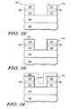
FIGS. 12-16 , which illustrate a first non-limiting embodiment of a method for making an SOI MOSFET in accordance with the teachings herein. - With reference to
FIG. 12 , the process begins with aninitial structure 220 which is similar in many respects to the structure ofFIG. 1 , and which comprises acarrier wafer 223, a buried oxide (BOX)layer 222, a patternedactive silicon layer 224, apad oxide layer 226, and a siliconnitride mask layer 228. A trench229 has been created in the structure through suitable photomasking and etching. The trench229 extends through the patternedsilicon layer 224, thepad oxide layer 226 and the siliconnitride mask layer 228. - The
carrier wafer 223 may be, for example, a silicon wafer, a germanium wafer, a SiGe wafer, or other suitable types of wafers or substrates as are known to the art. TheBOX layer 222 is preferably silicon dioxide, but may also comprise other dielectric materials as are known to the art. Thepad oxide layer 226 comprises an oxide which may be the same as, or different from, the oxide of theBOX layer 222, though in some embodiments thepad oxide layer 226 may be replaced by other dielectric materials. Thepad oxide layer 226 is preferably adapted to provide a suitable stress buffer to compensate for the differences in coefficients of thermal expansion in theactive silicon layer 224 and thesilicon nitride mask 228, and also serves as an adhesion promoter between thenitride mask 228 and theactive silicon layer 224. Thepad oxide layer 226 also protectssilicon layer 224 during the wet etching process used to remove the siliconnitride mask layer 228 after polishing. This wet etching is typically conducted with phosphoric acid, which is known to etch silicon. - The
active silicon layer 224 is the layer in which devices such as transistors will be built. It will be appreciated that, in some embodiments, theactive silicon layer 224 may actually include a plurality of layers and/or a plurality of materials. For example, theactive silicon layer 224 may be (but is not necessarily limited to) epitaxially grown silicon, epitaxially grown SiGe, or combinations thereof. In other embodiments, other semiconductor materials, such as, for example, Ge or SiGe, may be substituted for silicon in this layer. - In the
particular structure 220 depicted inFIG. 12 , the patternedactive silicon layer 224 has acover layer 244 disposed thereon which, in this example, comprises apad oxide layer 226 which is formed on the patternedactive silicon layer 224, and a siliconnitride mask layer 228 which is formed on thepad oxide layer 226. In other embodiments, all or a portion of thecover layer 244 may be removed in theinitial structure 220. Of course, one of ordinary skill in the art will appreciate that various other initial structures and cover layers are also possible. - Referring now to
FIG. 13 , anoxide liner 250 is formed on the exposed portions of the patternedactive silicon layer 224, typically to a thickness of about 80 Å at the bottom of the trench (due to the anisotropy of the deposition process, this results in a liner thickness of about 40 Å on the sidewalls of the trench). Preferably, theoxide liner 250 is formed through plasma enhanced chemical vapor deposition (PECVD) or high density plasma (HDP) deposition. - Referring now to
FIG. 14 , a layer ofpolysilicon 254 is then deposited over theoxide liner 250, preferably through thermal deposition in a furnace. The layer ofpolysilicon 254 is typically deposited to a thickness of about 100 Å to about 800 Å, preferably to a thickness of about 100 Å to about 600 Å, more preferably to a thickness of about 200 Å to about 400 Å, and most preferably to a thickness of about 300 Å. - After deposition of the
polysilicon layer 254, thepolysilicon layer 254 is etched back to formpolysilicon stressor structures 255 in the active trench as shown inFIG. 15 . While it is preferred that this is accomplished through an anisotropic etch without masking, in some embodiments, thepolysilicon layer 254 could be patterned and etched through the use of suitable photolithographic techniques. - Referring still to
FIG. 15 , a trench fillthermal oxide 256 is then formed over the structure. Thetrench fill oxide 256 is preferably a conformal layer. In a preferred process of forming thetrench fill oxide 256, a high density plasma chemical vapor deposition (HDP CVD) process is used. However, other processes for forming thetrench fill oxide 256 may also be used. Thetrench fill oxide 256 is preferably a dielectric material such as silicon dioxide. - As shown in
FIG. 16 , thepolysilicon stressor structures 255 are then subjected to at least partial oxidation. Since the oxidation product (silicon dioxide) has a larger volume than the original polysilicon of thestressor structures 255, this process results in the creation of compressive stress on theactive silicon regions 224. It is preferred that thetrench fill oxide 256 is formed before oxidation of the polysilicon stressor structures255 (or at least before oxidation of thestressor structures 255 is complete), since this provides a mass against which thestressor structures 255 can expand as oxidation occurs. - After deposition or formation of the
trench fill oxide 256, thepolysilicon stressor structures 255 may then be oxidized (or further oxidized) through one or more thermal cycles. The thermal cycles may include densification (the process of subjecting thetrench fill oxide 256 to a high temperature, typically within the range of 950° C. to 1200° C., to increase its density and/or improve its dielectric properties), sacrificial oxidation, double gate oxidation (DGO), or triple gate oxidation (TGO). - The improvements in MOSFET performance that are achievable with the methodologies described herein may be appreciated with respect to TABLE 1 below, which gives the piezoelectric resistance values for the NMOS and PMOS regions of a MOSFET device made in accordance with the method depicted in
FIGS. 12-14 . The values in bold typeface are tension values, and the values in italicized typeface are compression values. The units are percent improvement in the linear drive current of a device per 100 MPa of applied uniaxial stress compared to an unstressed device. The channel direction (SA), which is the direction the charge carriers are flowing from source to drain, is indicated in thedevice 301 shown inFIG. 17 . Thesource 303, drain305,active silicon layer 307,field oxide region 309 andpoly gate 311 are also shown.TABLE 1 Percentage Change in Drive Current Per 100 MPa of Uniaxial Stress Channel Stress Channel Width Width Vertical Channel (Bulk Stress Stress Stress Stress Direction Device Si) (SOI) (Bulk Si) (SOI) (Bulk Si) <110> NMOS 3.1 2.6 1.8 1.6 −5.3 <110> PMOS −7.2 −8.6 6.6 5.9 0.1 <100> NMOS 10.2 1.9 −5.3 1.4 −5.3 <100> PMOS −0.7 −2.3 0.1 −3.9 0.1 - It will be appreciated from the data set forth in TABLE 1 that the use of a polysilicon stressor structure provides the greatest improvement in drive current in the PMOS region of an SOI MOSFET device and when the stressor structure is aligned with the channel. This is so even though the use of polysilicon stressor structures slightly degrades the performance of the NMOS device, since the effect of the stressor structure in the PMOS region is the dominant effect with respect to overall CMOS performance. Hence, the use of polysilicon stressor structures in both regions provides a substantial improvement in device performance. Of course, one skilled in the art will appreciate that the use of a compressive stress material such as polysilicon could be used in the PMOS region in conjunction with the use of a tensile stress material such as nitride in the NMOS region to optimize overall CMOS performance.
- The data set forth in TABLE 1 also suggest a number of possible variations to the methodologies and structures described above. For example, rather than applying a polysilicon stressor structure to both the PMOS and NMOS regions of a MOSFET device, it will be appreciated that suitable masking and/or etching techniques could be utilized to restrict the formation of these structures to only the PMOS region, or to selectively remove the polysilicon stressor structures or polysilicon layer from the NMOS region. Of course, in a given implementation, the increased process complication attendant to the additional masking and/or etching steps would have to be weighed against the improvement in device performance gained by this process.
- Moreover, in some embodiments, one or more layers of nitride could be deposited which act in conjunction with the polysilicon to create dual stressor structures. Such structures could feature layer stacks comprising one or more layers of polysilicon and one or more layers of nitride, or could feature at least first and second distinct regions that are covered, respectively, by polysilicon and nitride. In such embodiments, the polysilicon stressor structure could act to provide compressive stress, while the nitride could act to prevent compressive stress from forming (or, put another way, could act as a tensile stressor structure). The use of nitride, particularly as a liner material, is also effective at preventing or minimizing the incidence of bird's beak structures (see, e.g.,
FIG. 11 ). - The data in TABLE 1 also indicate that the improvement in device performance in the channel direction comes to some extent at the expense of drive current in the width direction. In some embodiments, it may be possible to minimize degradation in device performance in the width direction by minimizing the width of the polysilicon stressor structure. A similar result may be achieved by applying nitride or another tensile stressor structure in the width direction of a PMOS device, while applying polysilicon as a compressive stressor structure in the channel direction. Here, it is to be noted that such a multidirectional approach may not be necessary for the NMOS device, since the data indicates that a tensile stressor structure such as nitride would improve device performance in both the channel and width directions.
- As previously noted, after deposition of the trench fill oxide, the device is preferably subjected to thermal cycling. The thermal cycling may include densification, which is typically conducted within the range of 950° C. to 1200° C. As also previously noted, nitride layers have been used in the art to suppress the formation of bird's beak structures (see
FIG. 11 and the accompanying text), and may be used in the devices and methodologies described herein (especially in the NMOS regions of these devices) to impart tensile stress to channel layers. It has now been discovered that the temperature and duration of the densification process used in conjunction with such nitride layers has an important effect on the performance characteristics of a MOSFET device, and especially on the drive current of the device. This effect may be appreciated with respect toFIG. 18 . - The graph in
FIG. 18 depicts the universal curve for a system of the type depicted inFIG. 11 . The universal curve measures the leakage current (IOFF) as a function of drive current (ION) for the device. The preferred region of the graph is toward the bottom left-hand corner, where IOFFis minimized and IONis maximized. The line denoted “SiN+HDT” represents the mean results achieved for a MOSFET device exposed to a peak densification temperature of 1150° C. for a duration of 15 minutes at this peak temperature, while the line denoted “SiN+LDT” represents the mean results achieved for a MOSFET device exposed to a peak densification temperature of 1000° C. and a duration of 15 minutes at this peak temperature. - As seen from the graph, there is a significant drop in drive current (about 10%) in going from the higher temperature densification process to the lower temperature densification process. Additional studies have shown that a maximum densification temperature as low as 900° C. can produce even further improvements in drive currents. Maximum densification temperatures below about 900° C. are not preferred, since it is found that adequate densification may not occur within this range, with the result that subsequent etch processes will consume excessive amounts of the trench fill oxide. However, at peak densification temperatures above about 900° C., densification is sufficient, and yet sufficiently low to permit the trench fill oxide to be etched at a faster rate than would be the case if the trench fill oxide were denser (that is, the etch rate is higher than would be the case if the trench fill oxide were densified at a higher peak temperature). This results in the proper amount of oxide recess below the surface of the active silicon. At the same time, top corner rounding of the active silicon layer is improved, which improves the reliability of the MOSFET device.
- Maximum densification temperatures above about 1050° C. are also not preferred, since it is found that the incidence of bird's beak structures begins to increase at these temperatures when a thermal oxidation step is part of the densification. Moreover, at temperatures above about 1050° C., the increased thermal stress in the trench fill oxide causes a shift in channel stress from tensile to compressive. This, in turn, degrades physical properties, such as ION, in the width direction of the channel.
- In light of the above, the preferred maximum temperature for densification is within the range of about 900° C. to about 1050° C., and is more preferably within the range of about 900° C. to about 1000° C. Most preferably, the maximum temperature for densification is within the range of about 900° C. to about 950° C. The duration of exposure of the device to this peak densification temperature is typically at least 5 minutes, preferably at least about 10 minutes, more preferably within the range of about 10 minutes to about 40 minutes, and most preferably within the range of about 15 minutes to about 30 minutes.
- The above description of the present invention is illustrative, and is not intended to be limiting. It will thus be appreciated that various additions, substitutions and modifications may be made to the above described embodiments without departing from the scope of the present invention. Accordingly, the scope of the present invention should be construed in reference to the appended claims.
Claims (20)
Priority Applications (1)
| Application Number | Priority Date | Filing Date | Title |
|---|---|---|---|
| US11/386,539US20070224772A1 (en) | 2006-03-21 | 2006-03-21 | Method for forming a stressor structure |
Applications Claiming Priority (1)
| Application Number | Priority Date | Filing Date | Title |
|---|---|---|---|
| US11/386,539US20070224772A1 (en) | 2006-03-21 | 2006-03-21 | Method for forming a stressor structure |
Publications (1)
| Publication Number | Publication Date |
|---|---|
| US20070224772A1true US20070224772A1 (en) | 2007-09-27 |
Family
ID=38534015
Family Applications (1)
| Application Number | Title | Priority Date | Filing Date |
|---|---|---|---|
| US11/386,539AbandonedUS20070224772A1 (en) | 2006-03-21 | 2006-03-21 | Method for forming a stressor structure |
Country Status (1)
| Country | Link |
|---|---|
| US (1) | US20070224772A1 (en) |
Cited By (39)
| Publication number | Priority date | Publication date | Assignee | Title |
|---|---|---|---|---|
| US20070235802A1 (en)* | 2006-04-05 | 2007-10-11 | Chartered Semiconductor Manufacturing Ltd | Method to control source/drain stressor profiles for stress engineering |
| US20070243692A1 (en)* | 2006-04-18 | 2007-10-18 | Micron Technology, Inc. | Methods of filling isolation trenches for semiconductor devices and resulting structures |
| US20080157404A1 (en)* | 2007-01-02 | 2008-07-03 | David Michael Fried | Trench structure and method for co-alignment of mixed optical and electron beam lithographic fabrication levels |
| US20080173972A1 (en)* | 2007-01-19 | 2008-07-24 | International Business Machines Corporation | Method of wafer thinning |
| US20090206407A1 (en)* | 2008-02-19 | 2009-08-20 | Anderson Brent A | Semiconductor devices having tensile and/or compressive stress and methods of manufacturing |
| US20090291540A1 (en)* | 2008-05-22 | 2009-11-26 | Da Zhang | CMOS Process with Optimized PMOS and NMOS Transistor Devices |
| US20090289280A1 (en)* | 2008-05-22 | 2009-11-26 | Da Zhang | Method for Making Transistors and the Device Thereof |
| US20100265275A1 (en)* | 2007-11-20 | 2010-10-21 | Koninklijke Philips Electronics N.V. | Backlighting system and display device |
| US8399310B2 (en) | 2010-10-29 | 2013-03-19 | Freescale Semiconductor, Inc. | Non-volatile memory and logic circuit process integration |
| US8658497B2 (en) | 2012-01-04 | 2014-02-25 | Freescale Semiconductor, Inc. | Non-volatile memory (NVM) and logic integration |
| US8669158B2 (en) | 2012-01-04 | 2014-03-11 | Mark D. Hall | Non-volatile memory (NVM) and logic integration |
| US8716781B2 (en) | 2012-04-09 | 2014-05-06 | Freescale Semiconductor, Inc. | Logic transistor and non-volatile memory cell integration |
| US8716089B1 (en) | 2013-03-08 | 2014-05-06 | Freescale Semiconductor, Inc. | Integrating formation of a replacement gate transistor and a non-volatile memory cell having thin film storage |
| US8728886B2 (en) | 2012-06-08 | 2014-05-20 | Freescale Semiconductor, Inc. | Integrating formation of a replacement gate transistor and a non-volatile memory cell using a high-k dielectric |
| US8741719B1 (en) | 2013-03-08 | 2014-06-03 | Freescale Semiconductor, Inc. | Integrating formation of a logic transistor and a non-volatile memory cell using a partial replacement gate technique |
| US8871598B1 (en) | 2013-07-31 | 2014-10-28 | Freescale Semiconductor, Inc. | Non-volatile memory (NVM) and high-k and metal gate integration using gate-first methodology |
| US8877585B1 (en) | 2013-08-16 | 2014-11-04 | Freescale Semiconductor, Inc. | Non-volatile memory (NVM) cell, high voltage transistor, and high-K and metal gate transistor integration |
| US8901632B1 (en) | 2013-09-30 | 2014-12-02 | Freescale Semiconductor, Inc. | Non-volatile memory (NVM) and high-K and metal gate integration using gate-last methodology |
| US8906764B2 (en) | 2012-01-04 | 2014-12-09 | Freescale Semiconductor, Inc. | Non-volatile memory (NVM) and logic integration |
| US8932925B1 (en) | 2013-08-22 | 2015-01-13 | Freescale Semiconductor, Inc. | Split-gate non-volatile memory (NVM) cell and device structure integration |
| US8951863B2 (en) | 2012-04-06 | 2015-02-10 | Freescale Semiconductor, Inc. | Non-volatile memory (NVM) and logic integration |
| US9006093B2 (en) | 2013-06-27 | 2015-04-14 | Freescale Semiconductor, Inc. | Non-volatile memory (NVM) and high voltage transistor integration |
| US9082650B2 (en) | 2013-08-21 | 2015-07-14 | Freescale Semiconductor, Inc. | Integrated split gate non-volatile memory cell and logic structure |
| US9082837B2 (en) | 2013-08-08 | 2015-07-14 | Freescale Semiconductor, Inc. | Nonvolatile memory bitcell with inlaid high k metal select gate |
| US9087913B2 (en) | 2012-04-09 | 2015-07-21 | Freescale Semiconductor, Inc. | Integration technique using thermal oxide select gate dielectric for select gate and apartial replacement gate for logic |
| US9112056B1 (en) | 2014-03-28 | 2015-08-18 | Freescale Semiconductor, Inc. | Method for forming a split-gate device |
| US9111865B2 (en) | 2012-10-26 | 2015-08-18 | Freescale Semiconductor, Inc. | Method of making a logic transistor and a non-volatile memory (NVM) cell |
| US9129996B2 (en) | 2013-07-31 | 2015-09-08 | Freescale Semiconductor, Inc. | Non-volatile memory (NVM) cell and high-K and metal gate transistor integration |
| US9129855B2 (en) | 2013-09-30 | 2015-09-08 | Freescale Semiconductor, Inc. | Non-volatile memory (NVM) and high-k and metal gate integration using gate-first methodology |
| US9136129B2 (en) | 2013-09-30 | 2015-09-15 | Freescale Semiconductor, Inc. | Non-volatile memory (NVM) and high-k and metal gate integration using gate-last methodology |
| US9231077B2 (en) | 2014-03-03 | 2016-01-05 | Freescale Semiconductor, Inc. | Method of making a logic transistor and non-volatile memory (NVM) cell |
| US9252152B2 (en) | 2014-03-28 | 2016-02-02 | Freescale Semiconductor, Inc. | Method for forming a split-gate device |
| US9252246B2 (en) | 2013-08-21 | 2016-02-02 | Freescale Semiconductor, Inc. | Integrated split gate non-volatile memory cell and logic device |
| US9257445B2 (en) | 2014-05-30 | 2016-02-09 | Freescale Semiconductor, Inc. | Method of making a split gate non-volatile memory (NVM) cell and a logic transistor |
| US9275864B2 (en) | 2013-08-22 | 2016-03-01 | Freescale Semiconductor,Inc. | Method to form a polysilicon nanocrystal thin film storage bitcell within a high k metal gate platform technology using a gate last process to form transistor gates |
| US9343314B2 (en) | 2014-05-30 | 2016-05-17 | Freescale Semiconductor, Inc. | Split gate nanocrystal memory integration |
| US9379222B2 (en) | 2014-05-30 | 2016-06-28 | Freescale Semiconductor, Inc. | Method of making a split gate non-volatile memory (NVM) cell |
| US9472418B2 (en) | 2014-03-28 | 2016-10-18 | Freescale Semiconductor, Inc. | Method for forming a split-gate device |
| US20190164819A1 (en)* | 2017-11-28 | 2019-05-30 | Taiwan Semiconductor Manufacturing Co., Ltd. | Liner structure in interlayer dielectric structure for semiconductor devices |
Citations (19)
| Publication number | Priority date | Publication date | Assignee | Title |
|---|---|---|---|---|
| US5512509A (en)* | 1993-11-23 | 1996-04-30 | Hyundai Electronics Industries Co., Ltd. | Method for forming an isolation layer in a semiconductor device |
| US6096621A (en)* | 1997-04-23 | 2000-08-01 | Elantec, Inc. | Polysilicon filled trench isolation structure for soi integrated circuits |
| US6118167A (en)* | 1997-11-13 | 2000-09-12 | National Semiconductor Corporation | Polysilicon coated nitride-lined shallow trench |
| US6297128B1 (en)* | 1999-01-29 | 2001-10-02 | Vantis Corporation | Process for manufacturing shallow trenches filled with dielectric material having low mechanical stress |
| US20010041421A1 (en)* | 1999-10-12 | 2001-11-15 | Park Tai-Su | Trench isolatoin regions having trench liners with recessed ends |
| US6396113B1 (en)* | 1999-11-19 | 2002-05-28 | Mitsubishi Denki Kabushiki Kaisha | Active trench isolation structure to prevent punch-through and junction leakage |
| US6410938B1 (en)* | 2001-04-03 | 2002-06-25 | Advanced Micro Devices, Inc. | Semiconductor-on-insulator device with nitrided buried oxide and method of fabricating |
| US20030013272A1 (en)* | 2001-07-03 | 2003-01-16 | Hong Soo-Jin | Trench device isolation structure and a method of forming the same |
| US20040038495A1 (en)* | 2002-07-30 | 2004-02-26 | Karsten Wieczorek | Method of providing a thick thermal oxide in trench isolation |
| US6825529B2 (en)* | 2002-12-12 | 2004-11-30 | International Business Machines Corporation | Stress inducing spacers |
| US20050101111A1 (en)* | 2003-05-09 | 2005-05-12 | Yee-Chia Yeo | SOI chip with mesa isolation and recess resistant regions |
| US20050142706A1 (en)* | 2000-08-17 | 2005-06-30 | Samsung Electronic Co., Ltd. | Method of preventing semiconductor layers from bending and semiconductor device formed thereby |
| US20050145937A1 (en)* | 2003-12-29 | 2005-07-07 | Kuang-Hsin Chen | STI liner for SOI structure |
| US20060110892A1 (en)* | 2004-11-22 | 2006-05-25 | Freescale Semiconductor, Inc. | Semiconductor process for forming stress absorbent shallow trench isolation structures |
| US20060220142A1 (en)* | 2005-03-31 | 2006-10-05 | Fujitsu Limited | Semiconductor device and manufacturing method thereof |
| US20070015347A1 (en)* | 2005-07-18 | 2007-01-18 | Texas Instruments Incorporated | Strain modulation employing process techniques for CMOS technologies |
| US20070059899A1 (en)* | 2004-02-19 | 2007-03-15 | Micron Technology, Inc. | Sub-micron space liner and filler process |
| US7271074B2 (en)* | 2002-10-08 | 2007-09-18 | X-Fab Semiconductor Foundries Ag | Trench insulation in substrate disks comprising logic semiconductors and power semiconductors |
| US20080185658A1 (en)* | 2005-07-15 | 2008-08-07 | International Business Machines Corporation | Buried Stress Isolation for High-Performance CMOS Technology |
- 2006
- 2006-03-21USUS11/386,539patent/US20070224772A1/ennot_activeAbandoned
Patent Citations (19)
| Publication number | Priority date | Publication date | Assignee | Title |
|---|---|---|---|---|
| US5512509A (en)* | 1993-11-23 | 1996-04-30 | Hyundai Electronics Industries Co., Ltd. | Method for forming an isolation layer in a semiconductor device |
| US6096621A (en)* | 1997-04-23 | 2000-08-01 | Elantec, Inc. | Polysilicon filled trench isolation structure for soi integrated circuits |
| US6118167A (en)* | 1997-11-13 | 2000-09-12 | National Semiconductor Corporation | Polysilicon coated nitride-lined shallow trench |
| US6297128B1 (en)* | 1999-01-29 | 2001-10-02 | Vantis Corporation | Process for manufacturing shallow trenches filled with dielectric material having low mechanical stress |
| US20010041421A1 (en)* | 1999-10-12 | 2001-11-15 | Park Tai-Su | Trench isolatoin regions having trench liners with recessed ends |
| US6396113B1 (en)* | 1999-11-19 | 2002-05-28 | Mitsubishi Denki Kabushiki Kaisha | Active trench isolation structure to prevent punch-through and junction leakage |
| US20050142706A1 (en)* | 2000-08-17 | 2005-06-30 | Samsung Electronic Co., Ltd. | Method of preventing semiconductor layers from bending and semiconductor device formed thereby |
| US6410938B1 (en)* | 2001-04-03 | 2002-06-25 | Advanced Micro Devices, Inc. | Semiconductor-on-insulator device with nitrided buried oxide and method of fabricating |
| US20030013272A1 (en)* | 2001-07-03 | 2003-01-16 | Hong Soo-Jin | Trench device isolation structure and a method of forming the same |
| US20040038495A1 (en)* | 2002-07-30 | 2004-02-26 | Karsten Wieczorek | Method of providing a thick thermal oxide in trench isolation |
| US7271074B2 (en)* | 2002-10-08 | 2007-09-18 | X-Fab Semiconductor Foundries Ag | Trench insulation in substrate disks comprising logic semiconductors and power semiconductors |
| US6825529B2 (en)* | 2002-12-12 | 2004-11-30 | International Business Machines Corporation | Stress inducing spacers |
| US20050101111A1 (en)* | 2003-05-09 | 2005-05-12 | Yee-Chia Yeo | SOI chip with mesa isolation and recess resistant regions |
| US20050145937A1 (en)* | 2003-12-29 | 2005-07-07 | Kuang-Hsin Chen | STI liner for SOI structure |
| US20070059899A1 (en)* | 2004-02-19 | 2007-03-15 | Micron Technology, Inc. | Sub-micron space liner and filler process |
| US20060110892A1 (en)* | 2004-11-22 | 2006-05-25 | Freescale Semiconductor, Inc. | Semiconductor process for forming stress absorbent shallow trench isolation structures |
| US20060220142A1 (en)* | 2005-03-31 | 2006-10-05 | Fujitsu Limited | Semiconductor device and manufacturing method thereof |
| US20080185658A1 (en)* | 2005-07-15 | 2008-08-07 | International Business Machines Corporation | Buried Stress Isolation for High-Performance CMOS Technology |
| US20070015347A1 (en)* | 2005-07-18 | 2007-01-18 | Texas Instruments Incorporated | Strain modulation employing process techniques for CMOS technologies |
Cited By (48)
| Publication number | Priority date | Publication date | Assignee | Title |
|---|---|---|---|---|
| US8017487B2 (en)* | 2006-04-05 | 2011-09-13 | Globalfoundries Singapore Pte. Ltd. | Method to control source/drain stressor profiles for stress engineering |
| US20070235802A1 (en)* | 2006-04-05 | 2007-10-11 | Chartered Semiconductor Manufacturing Ltd | Method to control source/drain stressor profiles for stress engineering |
| US8450775B2 (en) | 2006-04-05 | 2013-05-28 | Globalfoundries Singapore Pte. Ltd. | Method to control source/drain stressor profiles for stress engineering |
| US20070243692A1 (en)* | 2006-04-18 | 2007-10-18 | Micron Technology, Inc. | Methods of filling isolation trenches for semiconductor devices and resulting structures |
| US8304322B2 (en)* | 2006-04-18 | 2012-11-06 | Micron Technology, Inc. | Methods of filling isolation trenches for semiconductor devices and resulting structures |
| US20080157404A1 (en)* | 2007-01-02 | 2008-07-03 | David Michael Fried | Trench structure and method for co-alignment of mixed optical and electron beam lithographic fabrication levels |
| US7550361B2 (en)* | 2007-01-02 | 2009-06-23 | International Business Machines Corporation | Trench structure and method for co-alignment of mixed optical and electron beam lithographic fabrication levels |
| US20080173972A1 (en)* | 2007-01-19 | 2008-07-24 | International Business Machines Corporation | Method of wafer thinning |
| US20100265275A1 (en)* | 2007-11-20 | 2010-10-21 | Koninklijke Philips Electronics N.V. | Backlighting system and display device |
| US9368410B2 (en) | 2008-02-19 | 2016-06-14 | Globalfoundries Inc. | Semiconductor devices having tensile and/or compressive stress and methods of manufacturing |
| US20090206407A1 (en)* | 2008-02-19 | 2009-08-20 | Anderson Brent A | Semiconductor devices having tensile and/or compressive stress and methods of manufacturing |
| US8003454B2 (en) | 2008-05-22 | 2011-08-23 | Freescale Semiconductor, Inc. | CMOS process with optimized PMOS and NMOS transistor devices |
| US20090289280A1 (en)* | 2008-05-22 | 2009-11-26 | Da Zhang | Method for Making Transistors and the Device Thereof |
| US20090291540A1 (en)* | 2008-05-22 | 2009-11-26 | Da Zhang | CMOS Process with Optimized PMOS and NMOS Transistor Devices |
| US8877568B2 (en) | 2010-10-29 | 2014-11-04 | Freescale Semiconductor, Inc. | Methods of making logic transistors and non-volatile memory cells |
| US8399310B2 (en) | 2010-10-29 | 2013-03-19 | Freescale Semiconductor, Inc. | Non-volatile memory and logic circuit process integration |
| US8658497B2 (en) | 2012-01-04 | 2014-02-25 | Freescale Semiconductor, Inc. | Non-volatile memory (NVM) and logic integration |
| US8669158B2 (en) | 2012-01-04 | 2014-03-11 | Mark D. Hall | Non-volatile memory (NVM) and logic integration |
| US8906764B2 (en) | 2012-01-04 | 2014-12-09 | Freescale Semiconductor, Inc. | Non-volatile memory (NVM) and logic integration |
| US8951863B2 (en) | 2012-04-06 | 2015-02-10 | Freescale Semiconductor, Inc. | Non-volatile memory (NVM) and logic integration |
| US8716781B2 (en) | 2012-04-09 | 2014-05-06 | Freescale Semiconductor, Inc. | Logic transistor and non-volatile memory cell integration |
| US9087913B2 (en) | 2012-04-09 | 2015-07-21 | Freescale Semiconductor, Inc. | Integration technique using thermal oxide select gate dielectric for select gate and apartial replacement gate for logic |
| US8722493B2 (en) | 2012-04-09 | 2014-05-13 | Freescale Semiconductor, Inc. | Logic transistor and non-volatile memory cell integration |
| US8728886B2 (en) | 2012-06-08 | 2014-05-20 | Freescale Semiconductor, Inc. | Integrating formation of a replacement gate transistor and a non-volatile memory cell using a high-k dielectric |
| US9111865B2 (en) | 2012-10-26 | 2015-08-18 | Freescale Semiconductor, Inc. | Method of making a logic transistor and a non-volatile memory (NVM) cell |
| US8716089B1 (en) | 2013-03-08 | 2014-05-06 | Freescale Semiconductor, Inc. | Integrating formation of a replacement gate transistor and a non-volatile memory cell having thin film storage |
| US8741719B1 (en) | 2013-03-08 | 2014-06-03 | Freescale Semiconductor, Inc. | Integrating formation of a logic transistor and a non-volatile memory cell using a partial replacement gate technique |
| US9006093B2 (en) | 2013-06-27 | 2015-04-14 | Freescale Semiconductor, Inc. | Non-volatile memory (NVM) and high voltage transistor integration |
| US9129996B2 (en) | 2013-07-31 | 2015-09-08 | Freescale Semiconductor, Inc. | Non-volatile memory (NVM) cell and high-K and metal gate transistor integration |
| US8871598B1 (en) | 2013-07-31 | 2014-10-28 | Freescale Semiconductor, Inc. | Non-volatile memory (NVM) and high-k and metal gate integration using gate-first methodology |
| US9082837B2 (en) | 2013-08-08 | 2015-07-14 | Freescale Semiconductor, Inc. | Nonvolatile memory bitcell with inlaid high k metal select gate |
| US8877585B1 (en) | 2013-08-16 | 2014-11-04 | Freescale Semiconductor, Inc. | Non-volatile memory (NVM) cell, high voltage transistor, and high-K and metal gate transistor integration |
| US9252246B2 (en) | 2013-08-21 | 2016-02-02 | Freescale Semiconductor, Inc. | Integrated split gate non-volatile memory cell and logic device |
| US9082650B2 (en) | 2013-08-21 | 2015-07-14 | Freescale Semiconductor, Inc. | Integrated split gate non-volatile memory cell and logic structure |
| US8932925B1 (en) | 2013-08-22 | 2015-01-13 | Freescale Semiconductor, Inc. | Split-gate non-volatile memory (NVM) cell and device structure integration |
| US9275864B2 (en) | 2013-08-22 | 2016-03-01 | Freescale Semiconductor,Inc. | Method to form a polysilicon nanocrystal thin film storage bitcell within a high k metal gate platform technology using a gate last process to form transistor gates |
| US8901632B1 (en) | 2013-09-30 | 2014-12-02 | Freescale Semiconductor, Inc. | Non-volatile memory (NVM) and high-K and metal gate integration using gate-last methodology |
| US9136129B2 (en) | 2013-09-30 | 2015-09-15 | Freescale Semiconductor, Inc. | Non-volatile memory (NVM) and high-k and metal gate integration using gate-last methodology |
| US9129855B2 (en) | 2013-09-30 | 2015-09-08 | Freescale Semiconductor, Inc. | Non-volatile memory (NVM) and high-k and metal gate integration using gate-first methodology |
| US9231077B2 (en) | 2014-03-03 | 2016-01-05 | Freescale Semiconductor, Inc. | Method of making a logic transistor and non-volatile memory (NVM) cell |
| US9252152B2 (en) | 2014-03-28 | 2016-02-02 | Freescale Semiconductor, Inc. | Method for forming a split-gate device |
| US9112056B1 (en) | 2014-03-28 | 2015-08-18 | Freescale Semiconductor, Inc. | Method for forming a split-gate device |
| US9472418B2 (en) | 2014-03-28 | 2016-10-18 | Freescale Semiconductor, Inc. | Method for forming a split-gate device |
| US9257445B2 (en) | 2014-05-30 | 2016-02-09 | Freescale Semiconductor, Inc. | Method of making a split gate non-volatile memory (NVM) cell and a logic transistor |
| US9343314B2 (en) | 2014-05-30 | 2016-05-17 | Freescale Semiconductor, Inc. | Split gate nanocrystal memory integration |
| US9379222B2 (en) | 2014-05-30 | 2016-06-28 | Freescale Semiconductor, Inc. | Method of making a split gate non-volatile memory (NVM) cell |
| US20190164819A1 (en)* | 2017-11-28 | 2019-05-30 | Taiwan Semiconductor Manufacturing Co., Ltd. | Liner structure in interlayer dielectric structure for semiconductor devices |
| US11183423B2 (en)* | 2017-11-28 | 2021-11-23 | Taiwan Semiconductor Manufacturing Co., Ltd. | Liner structure in interlayer dielectric structure for semiconductor devices |
Similar Documents
| Publication | Publication Date | Title |
|---|---|---|
| US20070224772A1 (en) | Method for forming a stressor structure | |
| US20070249129A1 (en) | STI stressor integration for minimal phosphoric exposure and divot-free topography | |
| US8703565B2 (en) | Bottom-notched SiGe FinFET formation using condensation | |
| US7312134B2 (en) | Dual stressed SOI substrates | |
| US6680240B1 (en) | Silicon-on-insulator device with strained device film and method for making the same with partial replacement of isolation oxide | |
| US7405436B2 (en) | Stressed field effect transistors on hybrid orientation substrate | |
| US8907444B2 (en) | Stress-inducing structures, methods, and materials | |
| CN100461430C (en) | Semiconductor structures and methods of forming them | |
| US7700416B1 (en) | Tensile strained semiconductor on insulator using elastic edge relaxation and a sacrificial stressor layer | |
| US20050026390A1 (en) | Shallow trench filled with two or more dielectrics for isolation and coupling or for stress control | |
| KR100902105B1 (en) | Transistor of semiconductor device and manufacturing method thereof | |
| CN101312191A (en) | Semiconductor structures and methods of forming them | |
| WO2003050871A1 (en) | Mos semiconductor device | |
| US6617202B2 (en) | Method for fabricating a full depletion type SOI device | |
| US8766362B2 (en) | Shallow trench isolation for SOI structures combining sidewall spacer and bottom liner | |
| US7384833B2 (en) | Stress liner for integrated circuits | |
| US7626242B2 (en) | Shallow trench isolation process utilizing differential liners | |
| US7659599B2 (en) | Patterned silicon-on-insulator layers and methods for forming the same | |
| US8030148B2 (en) | Structured strained substrate for forming strained transistors with reduced thickness of active layer | |
| US20110210427A1 (en) | Strain memorization in strained soi substrates of semiconductor devices | |
| US7462549B2 (en) | Shallow trench isolation process and structure with minimized strained silicon consumption | |
| US7611937B2 (en) | High performance transistors with hybrid crystal orientations | |
| CN103426907A (en) | Semiconductor device and method for manufacturing the same | |
| JP2004047844A (en) | Semiconductor device and its manufacturing method | |
| US20130260532A1 (en) | Method for Manufacturing Semiconductor Device |
Legal Events
| Date | Code | Title | Description |
|---|---|---|---|
| AS | Assignment | Owner name:FREESCALE SEMICONDUCTOR, INC., TEXAS Free format text:ASSIGNMENT OF ASSIGNORS INTEREST;ASSIGNORS:HALL, MARK D.;MORA, RODE R.;TURNER, MICHAEL D.;AND OTHERS;REEL/FRAME:017932/0216 Effective date:20060321 | |
| AS | Assignment | Owner name:CITIBANK, N.A. AS COLLATERAL AGENT, NEW YORK Free format text:SECURITY AGREEMENT;ASSIGNORS:FREESCALE SEMICONDUCTOR, INC.;FREESCALE ACQUISITION CORPORATION;FREESCALE ACQUISITION HOLDINGS CORP.;AND OTHERS;REEL/FRAME:018855/0129 Effective date:20061201 Owner name:CITIBANK, N.A. AS COLLATERAL AGENT,NEW YORK Free format text:SECURITY AGREEMENT;ASSIGNORS:FREESCALE SEMICONDUCTOR, INC.;FREESCALE ACQUISITION CORPORATION;FREESCALE ACQUISITION HOLDINGS CORP.;AND OTHERS;REEL/FRAME:018855/0129 Effective date:20061201 | |
| AS | Assignment | Owner name:CITIBANK, N.A.,NEW YORK Free format text:SECURITY AGREEMENT;ASSIGNOR:FREESCALE SEMICONDUCTOR, INC.;REEL/FRAME:024085/0001 Effective date:20100219 Owner name:CITIBANK, N.A., NEW YORK Free format text:SECURITY AGREEMENT;ASSIGNOR:FREESCALE SEMICONDUCTOR, INC.;REEL/FRAME:024085/0001 Effective date:20100219 | |
| AS | Assignment | Owner name:CITIBANK, N.A., AS COLLATERAL AGENT,NEW YORK Free format text:SECURITY AGREEMENT;ASSIGNOR:FREESCALE SEMICONDUCTOR, INC.;REEL/FRAME:024397/0001 Effective date:20100413 Owner name:CITIBANK, N.A., AS COLLATERAL AGENT, NEW YORK Free format text:SECURITY AGREEMENT;ASSIGNOR:FREESCALE SEMICONDUCTOR, INC.;REEL/FRAME:024397/0001 Effective date:20100413 | |
| STCB | Information on status: application discontinuation | Free format text:ABANDONED -- FAILURE TO RESPOND TO AN OFFICE ACTION | |
| AS | Assignment | Owner name:FREESCALE SEMICONDUCTOR, INC., TEXAS Free format text:PATENT RELEASE;ASSIGNOR:CITIBANK, N.A., AS COLLATERAL AGENT;REEL/FRAME:037354/0225 Effective date:20151207 Owner name:FREESCALE SEMICONDUCTOR, INC., TEXAS Free format text:PATENT RELEASE;ASSIGNOR:CITIBANK, N.A., AS COLLATERAL AGENT;REEL/FRAME:037356/0143 Effective date:20151207 Owner name:FREESCALE SEMICONDUCTOR, INC., TEXAS Free format text:PATENT RELEASE;ASSIGNOR:CITIBANK, N.A., AS COLLATERAL AGENT;REEL/FRAME:037356/0553 Effective date:20151207 | |
| AS | Assignment | Owner name:MORGAN STANLEY SENIOR FUNDING, INC., MARYLAND Free format text:SECURITY AGREEMENT SUPPLEMENT;ASSIGNOR:NXP B.V.;REEL/FRAME:038017/0058 Effective date:20160218 | |
| AS | Assignment | Owner name:MORGAN STANLEY SENIOR FUNDING, INC., MARYLAND Free format text:CORRECTIVE ASSIGNMENT TO CORRECT THE REMOVE APPLICATION 12092129 PREVIOUSLY RECORDED ON REEL 038017 FRAME 0058. ASSIGNOR(S) HEREBY CONFIRMS THE SECURITY AGREEMENT SUPPLEMENT;ASSIGNOR:NXP B.V.;REEL/FRAME:039361/0212 Effective date:20160218 | |
| AS | Assignment | Owner name:MORGAN STANLEY SENIOR FUNDING, INC., MARYLAND Free format text:CORRECTIVE ASSIGNMENT TO CORRECT THE REMOVE APPLICATION 12681366 PREVIOUSLY RECORDED ON REEL 039361 FRAME 0212. ASSIGNOR(S) HEREBY CONFIRMS THE SECURITY AGREEMENT SUPPLEMENT;ASSIGNOR:NXP B.V.;REEL/FRAME:042762/0145 Effective date:20160218 Owner name:MORGAN STANLEY SENIOR FUNDING, INC., MARYLAND Free format text:CORRECTIVE ASSIGNMENT TO CORRECT THE REMOVE APPLICATION 12681366 PREVIOUSLY RECORDED ON REEL 038017 FRAME 0058. ASSIGNOR(S) HEREBY CONFIRMS THE SECURITY AGREEMENT SUPPLEMENT;ASSIGNOR:NXP B.V.;REEL/FRAME:042985/0001 Effective date:20160218 | |
| AS | Assignment | Owner name:NXP B.V., NETHERLANDS Free format text:RELEASE BY SECURED PARTY;ASSIGNOR:MORGAN STANLEY SENIOR FUNDING, INC.;REEL/FRAME:050745/0001 Effective date:20190903 | |
| AS | Assignment | Owner name:MORGAN STANLEY SENIOR FUNDING, INC., MARYLAND Free format text:CORRECTIVE ASSIGNMENT TO CORRECT THE REMOVE APPLICATION 12298143 PREVIOUSLY RECORDED ON REEL 042985 FRAME 0001. ASSIGNOR(S) HEREBY CONFIRMS THE SECURITY AGREEMENT SUPPLEMENT;ASSIGNOR:NXP B.V.;REEL/FRAME:051029/0001 Effective date:20160218 Owner name:MORGAN STANLEY SENIOR FUNDING, INC., MARYLAND Free format text:CORRECTIVE ASSIGNMENT TO CORRECT THE REMOVE APPLICATION 12298143 PREVIOUSLY RECORDED ON REEL 042762 FRAME 0145. ASSIGNOR(S) HEREBY CONFIRMS THE SECURITY AGREEMENT SUPPLEMENT;ASSIGNOR:NXP B.V.;REEL/FRAME:051145/0184 Effective date:20160218 Owner name:MORGAN STANLEY SENIOR FUNDING, INC., MARYLAND Free format text:CORRECTIVE ASSIGNMENT TO CORRECT THE REMOVE APPLICATION 12298143 PREVIOUSLY RECORDED ON REEL 039361 FRAME 0212. ASSIGNOR(S) HEREBY CONFIRMS THE SECURITY AGREEMENT SUPPLEMENT;ASSIGNOR:NXP B.V.;REEL/FRAME:051029/0387 Effective date:20160218 Owner name:MORGAN STANLEY SENIOR FUNDING, INC., MARYLAND Free format text:CORRECTIVE ASSIGNMENT TO CORRECT THE REMOVE APPLICATION12298143 PREVIOUSLY RECORDED ON REEL 039361 FRAME 0212. ASSIGNOR(S) HEREBY CONFIRMS THE SECURITY AGREEMENT SUPPLEMENT;ASSIGNOR:NXP B.V.;REEL/FRAME:051029/0387 Effective date:20160218 Owner name:MORGAN STANLEY SENIOR FUNDING, INC., MARYLAND Free format text:CORRECTIVE ASSIGNMENT TO CORRECT THE REMOVE APPLICATION12298143 PREVIOUSLY RECORDED ON REEL 042985 FRAME 0001. ASSIGNOR(S) HEREBY CONFIRMS THE SECURITY AGREEMENT SUPPLEMENT;ASSIGNOR:NXP B.V.;REEL/FRAME:051029/0001 Effective date:20160218 Owner name:MORGAN STANLEY SENIOR FUNDING, INC., MARYLAND Free format text:CORRECTIVE ASSIGNMENT TO CORRECT THE REMOVE APPLICATION 12298143 PREVIOUSLY RECORDED ON REEL 038017 FRAME 0058. ASSIGNOR(S) HEREBY CONFIRMS THE SECURITY AGREEMENT SUPPLEMENT;ASSIGNOR:NXP B.V.;REEL/FRAME:051030/0001 Effective date:20160218 Owner name:MORGAN STANLEY SENIOR FUNDING, INC., MARYLAND Free format text:CORRECTIVE ASSIGNMENT TO CORRECT THE REMOVE APPLICATION12298143 PREVIOUSLY RECORDED ON REEL 042762 FRAME 0145. ASSIGNOR(S) HEREBY CONFIRMS THE SECURITY AGREEMENT SUPPLEMENT;ASSIGNOR:NXP B.V.;REEL/FRAME:051145/0184 Effective date:20160218 |