US20070222081A1 - Surface treatment of inter-layer dielectric - Google Patents
Surface treatment of inter-layer dielectricDownload PDFInfo
- Publication number
- US20070222081A1 US20070222081A1US11/308,422US30842206AUS2007222081A1US 20070222081 A1US20070222081 A1US 20070222081A1US 30842206 AUS30842206 AUS 30842206AUS 2007222081 A1US2007222081 A1US 2007222081A1
- Authority
- US
- United States
- Prior art keywords
- interconnect structure
- ild
- gcib
- densified
- area
- Prior art date
- Legal status (The legal status is an assumption and is not a legal conclusion. Google has not performed a legal analysis and makes no representation as to the accuracy of the status listed.)
- Granted
Links
Images


Classifications
- H—ELECTRICITY
- H01—ELECTRIC ELEMENTS
- H01L—SEMICONDUCTOR DEVICES NOT COVERED BY CLASS H10
- H01L21/00—Processes or apparatus adapted for the manufacture or treatment of semiconductor or solid state devices or of parts thereof
- H01L21/70—Manufacture or treatment of devices consisting of a plurality of solid state components formed in or on a common substrate or of parts thereof; Manufacture of integrated circuit devices or of parts thereof
- H01L21/71—Manufacture of specific parts of devices defined in group H01L21/70
- H01L21/768—Applying interconnections to be used for carrying current between separate components within a device comprising conductors and dielectrics
- H01L21/76801—Applying interconnections to be used for carrying current between separate components within a device comprising conductors and dielectrics characterised by the formation and the after-treatment of the dielectrics, e.g. smoothing
- H01L21/76822—Modification of the material of dielectric layers, e.g. grading, after-treatment to improve the stability of the layers, to increase their density etc.
- H01L21/76825—Modification of the material of dielectric layers, e.g. grading, after-treatment to improve the stability of the layers, to increase their density etc. by exposing the layer to particle radiation, e.g. ion implantation, irradiation with UV light or electrons etc.
- H—ELECTRICITY
- H01—ELECTRIC ELEMENTS
- H01L—SEMICONDUCTOR DEVICES NOT COVERED BY CLASS H10
- H01L21/00—Processes or apparatus adapted for the manufacture or treatment of semiconductor or solid state devices or of parts thereof
- H01L21/02—Manufacture or treatment of semiconductor devices or of parts thereof
- H01L21/04—Manufacture or treatment of semiconductor devices or of parts thereof the devices having potential barriers, e.g. a PN junction, depletion layer or carrier concentration layer
- H01L21/18—Manufacture or treatment of semiconductor devices or of parts thereof the devices having potential barriers, e.g. a PN junction, depletion layer or carrier concentration layer the devices having semiconductor bodies comprising elements of Group IV of the Periodic Table or AIIIBV compounds with or without impurities, e.g. doping materials
- H01L21/30—Treatment of semiconductor bodies using processes or apparatus not provided for in groups H01L21/20 - H01L21/26
- H01L21/31—Treatment of semiconductor bodies using processes or apparatus not provided for in groups H01L21/20 - H01L21/26 to form insulating layers thereon, e.g. for masking or by using photolithographic techniques; After treatment of these layers; Selection of materials for these layers
- H01L21/3105—After-treatment
- H01L21/31058—After-treatment of organic layers
- H—ELECTRICITY
- H01—ELECTRIC ELEMENTS
- H01L—SEMICONDUCTOR DEVICES NOT COVERED BY CLASS H10
- H01L21/00—Processes or apparatus adapted for the manufacture or treatment of semiconductor or solid state devices or of parts thereof
- H01L21/70—Manufacture or treatment of devices consisting of a plurality of solid state components formed in or on a common substrate or of parts thereof; Manufacture of integrated circuit devices or of parts thereof
- H01L21/71—Manufacture of specific parts of devices defined in group H01L21/70
- H01L21/768—Applying interconnections to be used for carrying current between separate components within a device comprising conductors and dielectrics
- H01L21/76801—Applying interconnections to be used for carrying current between separate components within a device comprising conductors and dielectrics characterised by the formation and the after-treatment of the dielectrics, e.g. smoothing
- H01L21/76802—Applying interconnections to be used for carrying current between separate components within a device comprising conductors and dielectrics characterised by the formation and the after-treatment of the dielectrics, e.g. smoothing by forming openings in dielectrics
- H01L21/76807—Applying interconnections to be used for carrying current between separate components within a device comprising conductors and dielectrics characterised by the formation and the after-treatment of the dielectrics, e.g. smoothing by forming openings in dielectrics for dual damascene structures
- H01L21/76808—Applying interconnections to be used for carrying current between separate components within a device comprising conductors and dielectrics characterised by the formation and the after-treatment of the dielectrics, e.g. smoothing by forming openings in dielectrics for dual damascene structures involving intermediate temporary filling with material
- H—ELECTRICITY
- H01—ELECTRIC ELEMENTS
- H01L—SEMICONDUCTOR DEVICES NOT COVERED BY CLASS H10
- H01L21/00—Processes or apparatus adapted for the manufacture or treatment of semiconductor or solid state devices or of parts thereof
- H01L21/70—Manufacture or treatment of devices consisting of a plurality of solid state components formed in or on a common substrate or of parts thereof; Manufacture of integrated circuit devices or of parts thereof
- H01L21/71—Manufacture of specific parts of devices defined in group H01L21/70
- H01L21/768—Applying interconnections to be used for carrying current between separate components within a device comprising conductors and dielectrics
- H01L21/76801—Applying interconnections to be used for carrying current between separate components within a device comprising conductors and dielectrics characterised by the formation and the after-treatment of the dielectrics, e.g. smoothing
- H01L21/76802—Applying interconnections to be used for carrying current between separate components within a device comprising conductors and dielectrics characterised by the formation and the after-treatment of the dielectrics, e.g. smoothing by forming openings in dielectrics
- H01L21/76814—Applying interconnections to be used for carrying current between separate components within a device comprising conductors and dielectrics characterised by the formation and the after-treatment of the dielectrics, e.g. smoothing by forming openings in dielectrics post-treatment or after-treatment, e.g. cleaning or removal of oxides on underlying conductors
- H—ELECTRICITY
- H01—ELECTRIC ELEMENTS
- H01L—SEMICONDUCTOR DEVICES NOT COVERED BY CLASS H10
- H01L21/00—Processes or apparatus adapted for the manufacture or treatment of semiconductor or solid state devices or of parts thereof
- H01L21/70—Manufacture or treatment of devices consisting of a plurality of solid state components formed in or on a common substrate or of parts thereof; Manufacture of integrated circuit devices or of parts thereof
- H01L21/71—Manufacture of specific parts of devices defined in group H01L21/70
- H01L21/768—Applying interconnections to be used for carrying current between separate components within a device comprising conductors and dielectrics
- H01L21/76801—Applying interconnections to be used for carrying current between separate components within a device comprising conductors and dielectrics characterised by the formation and the after-treatment of the dielectrics, e.g. smoothing
- H01L21/76829—Applying interconnections to be used for carrying current between separate components within a device comprising conductors and dielectrics characterised by the formation and the after-treatment of the dielectrics, e.g. smoothing characterised by the formation of thin functional dielectric layers, e.g. dielectric etch-stop, barrier, capping or liner layers
- H01L21/76831—Applying interconnections to be used for carrying current between separate components within a device comprising conductors and dielectrics characterised by the formation and the after-treatment of the dielectrics, e.g. smoothing characterised by the formation of thin functional dielectric layers, e.g. dielectric etch-stop, barrier, capping or liner layers in via holes or trenches, e.g. non-conductive sidewall liners
Definitions
- the current inventionrelates to the field of semiconductor device manufacturing.
- itrelates to a process of providing treatment to surfaces of an interconnect structure after etching and before metallization.
- ultra-low dielectric constant (ULK) materialssuch as porous materials
- ILDinter-layer dielectric
- Interconnect structures made of metal lines or contacts, such as copper (Cu) for exampleare usually formed in and around the porous ULK ILD to connect semiconductor devices on the substrate.
- An interconnect structurewhich may include trenches and vias, may be formed by first creating a pattern of a three-dimensional interconnect structure in the ILD of a porous ULK material.
- the structure or patternmay be formed through processes such as lithography and etching, e.g., a reactive ion etching (RIE).
- RIEreactive ion etching
- a metal element or materialmay be deposited onto the trenches and/or vias of the formed structure pattern to create metal contact lines. Excess metal being deposited on the surface of the ULK ILD may be removed through a chemical mechanical planarization (CMP) process.
- CMPchemical mechanical planarization
- a Cu barrier metalsuch as Ta/TaN
- a conventional surface cleaning process designed or optimized for dense ILD buildmay cause element of the metal to penetrate or intrude into the porous material of the ULK ILD.
- This penetration or intrusion of metal element into porous ULK ILDmay cause performance degradation of the metal contacts formed thereon and, in a worst case, shortage of the semiconductor devices that the interconnect structure intends to connect.
- FIG. 1is a schematic illustration of a conventional interconnect structure as is known in the art
- FIG. 2is an illustration of a sample interconnect structure formed by following a conventional process as is known in the art
- FIG. 3is an illustration of another sample interconnect structure formed by following a conventional process as is known in the art
- FIG. 4is a schematic illustration of a method of forming an interconnect structure according to one embodiment of the invention.
- FIG. 5is a schematic illustration of a method of forming an interconnect structure according to another embodiment of the invention.
- FIG. 6is a schematic illustration of a method of forming an interconnect structure according to one embodiment of the invention.
- FIG. 7is a schematic illustration of a method of forming an interconnect structure according to another embodiment of the invention.
- FIG. 8is a schematic illustration of a method of forming an interconnect structure according to yet another embodiment of the invention.
- the current inventionprovides a process and method of densifying exposed areas of a porous ULK material at the bottom surfaces of an interconnect structure.
- the surface treatment of densificationmay be performed through irradiation, and the irradiation may be conducted by applying a Gas Cluster Ion Beam (GCIB).
- GCIBGas Cluster Ion Beam
- the size of a typical gas cluster used in the GCIB processmay be around, e.g., 5 nm, which is bigger than the size of a typical pore, which is around, e.g., 1 ⁇ 2 nm, inside a porous ULK material. Therefore, surface treatment by a GCIB process may not cause changes in the property of the bulk ULK material. In the mean time, the GCIB surface treatment may create a smooth layer of densified surface in the ULK dielectric material.
- the thickness of a densified layermay be controlled preferably by an acceleration voltage used in the GCIB process.
- the thickness of a densified layermay be from 10 ⁇ to 5000 ⁇ , and may be preferably in the range of 50 ⁇ -250 ⁇ .
- a conventional metallization processmay follow by first cleaning the surface of the interconnect structure, and then depositing a metal liner followed by a metal filler in the trench and/or via areas of the interconnect structure. Because the metallization process will now experience a “dense” ILD at the bottom of the trench and/or via, it may not cause roughness to the bottom surface or elements of the metal liner to intrude or penetrate into the underneath porous ULK ILD material. After the build of the interconnect structure is completed, the densified layer may remain inside the porous ILD material. In addition, embodiment of the present invention may enable a dual damascene build for both metal line and via in a porous ULK ILD material.
- Embodiments of the present inventionprovide a process or method of forming an interconnect structure on an inter-layer dielectric material.
- the methodincludes steps of providing treatment to an exposed area of the ILD material to create a densified area, and metallizing the densified area.
- the exposed areais a bottom surface of a trench created in the ILD material. According to another embodiment, the exposed area is part of a bottom surface of a trench or via created in the ILD material.
- the ILD materialmay be a porous material of ultra-low dielectric constant (ULK), and may be a silicon dioxide (SiO 2 ), a silicon oxycarbide (SiCOH), a methylsilsesquioxane (MSQ), a hydrosilsequioxane, a hydrogenated amorphous silicon carbide (SiCH), a hydrogenated amorphous silicon carbon nitride (SiCNH), or a silicon nitride (SiNx).
- ULKultra-low dielectric constant
- SiO 2silicon dioxide
- SiCOHsilicon oxycarbide
- MSQmethylsilsesquioxane
- hydrosilsequioxanea hydrogenated amorphous silicon carbide
- SiCNHhydrogenated amorphous silicon carbon nitride
- SiNxsilicon nitride
- Embodiments of the present inventionmay further provide a method of treating the exposed area of the ILD material by irradiating the exposed area using a GCIB.
- the GCIBmay be used at a dosage of approximately between 0.1 and 10.0 ⁇ 10 15 ion-clusters/cm 2 , and preferably between 0.5 and 2.5 ⁇ 10 15 ion-clusters/cm 2 .
- the GCIBmay be accelerated at a voltage of approximately between 1.0 and 60 KeV, and preferably between 5 and 15 KeV.
- the GCIBmay be generated through a pure or a mixture of inert and reactive gases.
- the inert gasesmay include one or more gases of argon, neon, krypton, xenon, radon, nitrogen, and oxygen.
- the densified areamay have a layer of thickness from 10 ⁇ to 5000 ⁇ , and preferably from 500 ⁇ to 250 ⁇ .
- Embodiments of the present inventionmay further provide a method of forming a bottom surface of the interconnect structure to create an exposed area of the ILD material.
- Embodiments of the present inventionmay provide an interconnect structure in a semiconductor chip for connecting one or more semiconductor devices.
- the interconnect structuremay include at least one densified area on a surface of an ILD material, and the densified area may be formed through irradiation treatment of the ILD material with a GCIB.
- the densified areamay include a bottom surface of a trench formed in the ILD material. According to another embodiment, the densified area may include part of a bottom surface of a via created in the ILD material.
- the interconnect structuremay further include a metal liner deposited on top of the densified area and a metal filler deposited on top of the metal liner, and the ILD material may be a silicon dioxide (SiO2), silicon oxycarbide (SiCOH), methylsilsesquioxane (MSQ), hydrosilsequioxane, hydrogenated amorphous silicon carbide (SiCH), hydrogenated amorphous silicon carbon nitride (SiCNH), or silicon nitride (SiNx).
- SiO2silicon dioxide
- SiCOHsilicon oxycarbide
- MSQmethylsilsesquioxane
- hydrosilsequioxanehydrogenated amorphous silicon carbide
- SiCNHhydrogenated amorphous silicon carbon nitride
- SiNxsilicon nitride
- Embodiment of the inventionmay provide a semiconductor device having at least one interconnect structure formed on an ILD material.
- the interconnect structuremay include one or more densified areas formed on one or more bottom surfaces of the interconnect structure.
- At least one of the densified areasmay form a layer, and the layer may have a thickness from 10 ⁇ to 500 ⁇ , and preferably from 50 ⁇ to 250 ⁇ .
- manufacture of a semiconductor devicemay include processing of, for example, a front end of line (FEOL) and a back end of line (BEOL).
- FEOLfront end of line
- BEOLback end of line
- semiconductor devicessuch as, for example, switches and logic gates may be produced. These devices may be interconnected through one or more interconnect structures.
- the interconnect structuresmay be produced through a BEOL processing.
- a conventional BEOL processingmay include steps such as, for example, cap deposition, ILD deposition, hard mask or photo-mask deposition, lithography, and etching, among other steps.
- stepssuch as, for example, cap deposition, ILD deposition, hard mask or photo-mask deposition, lithography, and etching, among other steps.
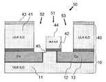
- FIG. 1is a schematic illustration of an interconnect structure as is known in the art.
- Interconnect structure 30may be created in an ULK ILD layer 20 , which may be formed on top of a prior ULK ILD layer 10 .
- ULK ILD Layer 10may include a porous material 11 , and thereon may be formed one or more interconnect structures such as, for example, metal contact or metal filler 13 deposited or filled on top of barrier metal film or liner 12 .
- ULK ILD layer 20may include a porous material 21 .
- Interconnect structure 30may include metal contact or metal filler 23 filled or deposited on top of barrier metal film or liner 22 .
- a liner 22which may not have a smooth surface and often have a rough interface with porous material 21 underneath it.
- the surface of porous material 21may be damaged during the plasma cleaning process and spike-like extrusions such as, for example, “spikes” 31 and 32 as illustrated in FIG. 1 may penetrate into porous material 21 underneath liner 22 .
- spike-like extrusionssuch as, for example, “spikes” 31 and 32 as illustrated in FIG. 1 may penetrate into porous material 21 underneath liner 22 .
- metal elements of liner 22may penetrate into “holes” of porous ULK material 21 .
- This roughness between the metal interconnect structure 30 and its underlining inter-layer dielectricmay cause performance degradation of the metal contact or interconnect. For example, in one instance, a deep “spike” may cause shortage among different semiconductor devices.
- FIG. 2is an illustration of a sample interconnect structure formed by following a conventional process as is known in the art.
- a plasma sputtering clean action or processwhich is normally applied to the surface before the deposition of a barrier metal film or liner for the formation of trenches and vias, caused damages to the porous material. This results in the roughness of metal liner at the surface of the ILD layer forming the bottom of a trench, as evidenced by extrusion or “spike” 31 .
- FIG. 3is an illustration of another sample interconnect structure formed by following a conventional process as is known in the art.
- extrusion or “spike” 32 in FIG. 3indicates that metal elements of a barrier metal file or liner of an interconnect structure in the current (top) ULK ILD layer may have penetrated or intruded into the porous material of a prior (bottom) ULK ILD layer.
- the porous material of bottom ULK ILD layermay have been exposed at the bottom of the via of the interconnect structure in the top ULK ILD layer, due to a misalignment, between the two different ILD layers, caused during the patterning process of vias.
- issues relating to metal intrusion into a neighboring porous ULK ILD layermay be resolved by applying a post RIE surface treatment of the ILD layer.
- the surface treatmentmay be applied after an area for interconnect structure is created through etching but before a subsequent conventional metallization process is applied.
- the surface treatmentmay seal at least some pores of the ULK ILD layer, and therefore may increase a density of the ULK material in a region close to the proximity of the surface, which in turn may enhance resistance of the surface to possible chemical and mechanical damages caused by subsequent processing steps in the formation of the interconnect structure.
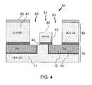
- FIG. 4is a schematic illustration of a method of forming an interconnect structure according to one embodiment of the invention.
- Interconnect structure 50may be created in a porous ULK ILD layer 40 which may be on top of a porous ULK ILD layer 10 of a prior layer.
- layer 40may or may not be an ULK ILD layer.
- ULK ILD layer 40may or may not be on top of another ULK ILD layer such as ULK ILD layer 10 .
- ULK ILD layer 10may have an interconnect structure formed thereon such as, for example, a metal contact 13 deposited or plated or filled on top of a barrier metal film or liner 12 .
- ULK ILD layer 10may not be and/or may not necessarily contain any interconnect structures at all.
- Interconnect structure 50may be formed through processing steps as briefly described below.
- a cap layer 42may be formed on ULK ILD layer 10 through, for example, a sputtering deposition process.
- a layer of porous ULK material 41may be deposited or formed to create an ILD layer.
- a structure of interconnect structure 50may be created in ULK ILD layer 41 , including a region 51 for forming a trench and regions 52 and 53 for forming vias, through processes such as, for example, selective etching as described below in detail.
- a layer of photon-sensitive materialmay be first applied on top of ULK ILD layer 41 .
- a lithographic processing techniquemay be subsequently used to create a photo-mask 43 out of the photon-sensitive layer of material.
- Photo-mask 43may include a desired pattern of trenches and/or vias to be created in ULK ILD layer 41 .
- ULK ILD layer 41 in the area defined by a trenchmay be subsequently etched away to form a trench region 51 .
- ULK ILD layer 41 and cap layer 42in areas defined by vias, may be etched away to form regions for vias 52 and 53 .
- regions for trench 51 and vias 52 and 53may be formed partially through same etching steps. But the invention is not limited in this respect and regions for trench 51 and visa 52 and 53 may be formed in different and/or separate steps.
- the etchingmay be a reactive ion etching process but the invention is not limited in this respect either, and other etching process such as a wet etching process may be used.
- trench region 51may create and expose a surface 44 of porous ULK material 41 .
- misalignment between current and prior levels of interconnect layers in a process of creating vias through lithographymay cause exposure of a part of porous ULK material 45 of a prior ILD layer, for example, ULK ILD layer 10 , as shown in FIG. 4 .
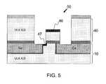
- FIG. 5is a schematic illustration of a method of forming an interconnect structure according to another embodiment of the invention.
- exposed surfaces of porous materials of layer 10 and layer 40may be treated, according to one embodiment, to create a layer of densified areas.
- exposed surfaces 44 and 45 ( FIG. 4 ) of porous materials 41 and 11may be treated to create densified areas 46 and 47 , respectively, which may be subsequently used to prevent metal elements of a liner, such as liner 48 ( FIG. 6 ) to be applied later, from penetrating into porous materials 41 and 11 .
- linersuch as liner 48 ( FIG. 6 )
- the surface treatmentmay be conducted by using a gas cluster ion beam (GCIB) to bombard exposed surfaces of the porous materials.
- GCIBgas cluster ion beam
- a process of applying GCIBmay be a low temperature process where large clusters of ions are used to bombard the surface of the porous materials.
- the ion beammay be directional, which enables the bombardment of very specific areas of interconnect structure 50 to create densified area 46 upon which a trench is to be formed, and/or densified area 47 upon which a via is formed later, as are illustrated in FIGS. 6-8 .
- porous ULK materials used as an ILD layermay be designed or selected, and/or to a certain extent optimally selected, to have sizes of pore diameters ranging from, for example, 1-2 nm in order to reduce and/or prevent line to line conduction paths.
- the size of ion clusters used in a GCIB processmay be in the order of a few nanometers, for example, 5 nm.
- the inventionis not limited in this respect, and the size of the ion clusters may vary depending on, for example, conditions of the GCIB process.
- a surface treatment by the GCIB processmay densify only a layer of the porous material in proximity to the surface and thus may not cause changes to the property of the bulk ULK material.
- a surface treatment by a conventional plasma processwill cause property changes of the bulk porous ULK material in the majority and in worst cases the entire thickness of the ILD layer. This may inadvertently offset some of the advantages of using porous ULK materials as an ILD layer.
- the GCIB processmay be adjusted, and/or to a certain extent optimized, by varying a dosage of the ions and/or an accelerating voltage for the ions.
- a dosage of the ions and/or an accelerating voltage for the ionsmay be used.
- benign elements or a mixture of benign and other elementsmay be used.
- some ion clustersmay include inert gas molecules such as, nitrogen, argon, or other pure gases and/or a mixture of different gases.
- thickness of the densification area or regionmay be determined by the acceleration voltage of the ion clusters.
- the thickness of a densified area or regionmay range between 50-250 ⁇ for BEOL interconnect purposes.
- the inventionis not limited in this respect and other thickness may be used for desired performance.
- the post RIE interconnect structure 50has now densified regions 46 at the bottom of the trench and 47 under the misaligned via. These densified regions 46 and 47 may be more resistant to possible chemical and/or physical damages which may occur during subsequent processing.
- FIG. 6is a schematic illustration of a method of forming an interconnect structure according to one embodiment of the invention.
- a barrier metal film or liner 48may be deposited onto the surfaces including regions, such as regions 51 , 52 and 53 ( FIG. 4 ), that are etched away for the formation of trenches and vias.
- aggressive sputtering and/or etch processesmay be applied to clean up the bottom surfaces of the trenches and vias, including the removal of at least part of the densified surface areas 46 and 47 .
- the GCIB process treated areas 46 and 47may withstand an intense processing that is typically used for dense ILD materials. As a result, smooth surfaces at the bottom of interconnect structure 50 may be maintained by densified areas 46 and 47 .
- the barrier metal film or liner 48 deposited subsequently at the trench bottom and in the area of the misaligned viamay continue to have a relatively smooth profile.
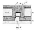
- FIG. 7is a schematic illustration of a method of forming an interconnect structure according to another embodiment of the invention.
- a metal element 49for example, copper (Cu) that is suitable for interconnecting semiconductor devices may be deposited or filled in the area etched for interconnect structure 50 and to be used as metal contact.
- Metal element 49may fill up interconnect structure 50 and in one embodiment may be excessively deposited onto other parts of ILD layer 40 as shown in FIG. 7 .
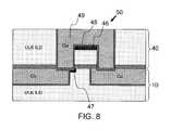
- FIG. 8is a schematic illustration of a method of forming an interconnect structure according to yet another embodiment of the invention.
- surface of the plated interconnect structure 50 or surface of ILD layer 40may be subjected to a planarization process such as, for example a CMP process, to remove excess metal element 49 and other processing related layers such as, for example, photo-mask layer 43 ( FIG. 4 ) and/or liner 48 outside interconnect structure 50 .
- the CMP processmay prepare the surface of ILD layer 40 for a further processing such as, for example, for the formation of a subsequent layer of interconnect.
Landscapes
- Engineering & Computer Science (AREA)
- Physics & Mathematics (AREA)
- Condensed Matter Physics & Semiconductors (AREA)
- General Physics & Mathematics (AREA)
- Manufacturing & Machinery (AREA)
- Computer Hardware Design (AREA)
- Microelectronics & Electronic Packaging (AREA)
- Power Engineering (AREA)
- Plasma & Fusion (AREA)
- Internal Circuitry In Semiconductor Integrated Circuit Devices (AREA)
Abstract
Description
- The current invention relates to the field of semiconductor device manufacturing. In particular, it relates to a process of providing treatment to surfaces of an interconnect structure after etching and before metallization.
- Recent rapid advancement in semiconductor technology has brought the advent of very large scale integrated (VLSI) as well as ultra large scale integrated (ULSI) circuitries, resulting in integration of more devices into smaller areas on a single semiconductor substrate. In order to further enhance performance of the VLSI and/or ULSI circuitries, ultra-low dielectric constant (ULK) materials, such as porous materials, are being used as inter-layer dielectric (ILD) to further reduce capacitance such as, for example, inter-layer capacitance and/or other parasitic capacitance that may be undesirable to the performance such as speed of the VLSI and/or ULSI circuitries. Interconnect structures made of metal lines or contacts, such as copper (Cu) for example, are usually formed in and around the porous ULK ILD to connect semiconductor devices on the substrate.
- An interconnect structure, which may include trenches and vias, may be formed by first creating a pattern of a three-dimensional interconnect structure in the ILD of a porous ULK material. As is known in the art, the structure or pattern may be formed through processes such as lithography and etching, e.g., a reactive ion etching (RIE). Subsequently, a metal element or material may be deposited onto the trenches and/or vias of the formed structure pattern to create metal contact lines. Excess metal being deposited on the surface of the ULK ILD may be removed through a chemical mechanical planarization (CMP) process. On the other hand, it is also known in the art that depositing a Cu barrier metal (liner), such as Ta/TaN, onto a surface of a porous ULK ILD using a conventional surface cleaning process designed or optimized for dense ILD build may cause element of the metal to penetrate or intrude into the porous material of the ULK ILD. This penetration or intrusion of metal element into porous ULK ILD may cause performance degradation of the metal contacts formed thereon and, in a worst case, shortage of the semiconductor devices that the interconnect structure intends to connect.
- The present invention will be understood and appreciated more fully from the following detailed description of the invention, taken in conjunction with the accompanying drawings of which:
FIG. 1 is a schematic illustration of a conventional interconnect structure as is known in the art;FIG. 2 is an illustration of a sample interconnect structure formed by following a conventional process as is known in the art;FIG. 3 is an illustration of another sample interconnect structure formed by following a conventional process as is known in the art;FIG. 4 is a schematic illustration of a method of forming an interconnect structure according to one embodiment of the invention;FIG. 5 is a schematic illustration of a method of forming an interconnect structure according to another embodiment of the invention;FIG. 6 is a schematic illustration of a method of forming an interconnect structure according to one embodiment of the invention;FIG. 7 is a schematic illustration of a method of forming an interconnect structure according to another embodiment of the invention; andFIG. 8 is a schematic illustration of a method of forming an interconnect structure according to yet another embodiment of the invention.- It will be appreciated that for simplicity and clarity of illustration, elements shown in the drawings have not necessarily been drawn to scale. For example, the dimensions of some of the elements may be exaggerated relative to other elements for clarity purpose.
- The current invention provides a process and method of densifying exposed areas of a porous ULK material at the bottom surfaces of an interconnect structure. The surface treatment of densification may be performed through irradiation, and the irradiation may be conducted by applying a Gas Cluster Ion Beam (GCIB).
- According to one embodiment of the invention, the size of a typical gas cluster used in the GCIB process may be around, e.g., 5 nm, which is bigger than the size of a typical pore, which is around, e.g., 1˜2 nm, inside a porous ULK material. Therefore, surface treatment by a GCIB process may not cause changes in the property of the bulk ULK material. In the mean time, the GCIB surface treatment may create a smooth layer of densified surface in the ULK dielectric material. According to one embodiment of the invention, the thickness of a densified layer may be controlled preferably by an acceleration voltage used in the GCIB process. According to another embodiment, the thickness of a densified layer may be from 10 Å to 5000 Å, and may be preferably in the range of 50 Å-250 Å.
- After the surface treatment through densification, a conventional metallization process may follow by first cleaning the surface of the interconnect structure, and then depositing a metal liner followed by a metal filler in the trench and/or via areas of the interconnect structure. Because the metallization process will now experience a “dense” ILD at the bottom of the trench and/or via, it may not cause roughness to the bottom surface or elements of the metal liner to intrude or penetrate into the underneath porous ULK ILD material. After the build of the interconnect structure is completed, the densified layer may remain inside the porous ILD material. In addition, embodiment of the present invention may enable a dual damascene build for both metal line and via in a porous ULK ILD material.
- Embodiments of the present invention provide a process or method of forming an interconnect structure on an inter-layer dielectric material. The method includes steps of providing treatment to an exposed area of the ILD material to create a densified area, and metallizing the densified area.
- According to one embodiment, the exposed area is a bottom surface of a trench created in the ILD material. According to another embodiment, the exposed area is part of a bottom surface of a trench or via created in the ILD material.
- According to embodiments of the invention, the ILD material may be a porous material of ultra-low dielectric constant (ULK), and may be a silicon dioxide (SiO2), a silicon oxycarbide (SiCOH), a methylsilsesquioxane (MSQ), a hydrosilsequioxane, a hydrogenated amorphous silicon carbide (SiCH), a hydrogenated amorphous silicon carbon nitride (SiCNH), or a silicon nitride (SiNx).
- Embodiments of the present invention may further provide a method of treating the exposed area of the ILD material by irradiating the exposed area using a GCIB.
- According to one embodiment, the GCIB may be used at a dosage of approximately between 0.1 and 10.0×10¹⁵ion-clusters/cm2, and preferably between 0.5 and 2.5×10¹⁵ion-clusters/cm2.
- According to another embodiment, the GCIB may be accelerated at a voltage of approximately between 1.0 and 60 KeV, and preferably between 5 and 15 KeV.
- According to yet another embodiment, the GCIB may be generated through a pure or a mixture of inert and reactive gases. The inert gases may include one or more gases of argon, neon, krypton, xenon, radon, nitrogen, and oxygen.
- According to one embodiment of the invention, the densified area may have a layer of thickness from 10 Å to 5000 Å, and preferably from 500 Å to 250 Å.
- Embodiments of the present invention may further provide a method of forming a bottom surface of the interconnect structure to create an exposed area of the ILD material.
- Embodiments of the present invention may provide an interconnect structure in a semiconductor chip for connecting one or more semiconductor devices. The interconnect structure may include at least one densified area on a surface of an ILD material, and the densified area may be formed through irradiation treatment of the ILD material with a GCIB.
- According to one embodiment, the densified area may include a bottom surface of a trench formed in the ILD material. According to another embodiment, the densified area may include part of a bottom surface of a via created in the ILD material.
- According to one embodiment, the interconnect structure may further include a metal liner deposited on top of the densified area and a metal filler deposited on top of the metal liner, and the ILD material may be a silicon dioxide (SiO2), silicon oxycarbide (SiCOH), methylsilsesquioxane (MSQ), hydrosilsequioxane, hydrogenated amorphous silicon carbide (SiCH), hydrogenated amorphous silicon carbon nitride (SiCNH), or silicon nitride (SiNx).
- Embodiment of the invention may provide a semiconductor device having at least one interconnect structure formed on an ILD material. The interconnect structure may include one or more densified areas formed on one or more bottom surfaces of the interconnect structure.
- According to one embodiment, at least one of the densified areas may form a layer, and the layer may have a thickness from 10 Å to 500 Å, and preferably from 50 Å to 250 Å.
- As is known in the art, manufacture of a semiconductor device may include processing of, for example, a front end of line (FEOL) and a back end of line (BEOL). During a FEOL processing, semiconductor devices such as, for example, switches and logic gates may be produced. These devices may be interconnected through one or more interconnect structures. The interconnect structures may be produced through a BEOL processing.
- A conventional BEOL processing may include steps such as, for example, cap deposition, ILD deposition, hard mask or photo-mask deposition, lithography, and etching, among other steps. For the interest of not obscuring the presentation of the essences of present invention, processing steps that are well known in the art may not be described below in detail, but rather the following description will focus on the distinctive elements of the present invention.
FIG. 1 is a schematic illustration of an interconnect structure as is known in the art.Interconnect structure 30 may be created in anULK ILD layer 20, which may be formed on top of a priorULK ILD layer 10.ULK ILD Layer 10 may include aporous material 11, and thereon may be formed one or more interconnect structures such as, for example, metal contact ormetal filler 13 deposited or filled on top of barrier metal film orliner 12. Similarly,ULK ILD layer 20 may include aporous material 21.Interconnect structure 30 may include metal contact or metal filler23 filled or deposited on top of barrier metal film or liner22.- During a metallization process, due to a plasma cleaning process which is typically employed in the creating of interconnections in a dense ILD material, in and around an area between metal contact23 and
porous material 21, there may be formed a liner22 which may not have a smooth surface and often have a rough interface withporous material 21 underneath it. As is known in the art, the surface ofporous material 21 may be damaged during the plasma cleaning process and spike-like extrusions such as, for example, “spikes”31 and32 as illustrated inFIG. 1 may penetrate intoporous material 21 underneath liner22. In other words, metal elements of liner22 may penetrate into “holes” ofporous ULK material 21. This roughness between themetal interconnect structure 30 and its underlining inter-layer dielectric may cause performance degradation of the metal contact or interconnect. For example, in one instance, a deep “spike” may cause shortage among different semiconductor devices. FIG. 2 is an illustration of a sample interconnect structure formed by following a conventional process as is known in the art. As described above with regard toFIG. 1 , due to the porous nature of ULK material of the ILD layer, a plasma sputtering clean action or process, which is normally applied to the surface before the deposition of a barrier metal film or liner for the formation of trenches and vias, caused damages to the porous material. This results in the roughness of metal liner at the surface of the ILD layer forming the bottom of a trench, as evidenced by extrusion or “spike”31.FIG. 3 is an illustration of another sample interconnect structure formed by following a conventional process as is known in the art. As described above with regard toFIG. 1 , the existence of extrusion or “spike”32 inFIG. 3 indicates that metal elements of a barrier metal file or liner of an interconnect structure in the current (top) ULK ILD layer may have penetrated or intruded into the porous material of a prior (bottom) ULK ILD layer. The porous material of bottom ULK ILD layer may have been exposed at the bottom of the via of the interconnect structure in the top ULK ILD layer, due to a misalignment, between the two different ILD layers, caused during the patterning process of vias.- According to embodiments of the invention, issues relating to metal intrusion into a neighboring porous ULK ILD layer may be resolved by applying a post RIE surface treatment of the ILD layer. The surface treatment may be applied after an area for interconnect structure is created through etching but before a subsequent conventional metallization process is applied. According to one embodiment of the invention, the surface treatment may seal at least some pores of the ULK ILD layer, and therefore may increase a density of the ULK material in a region close to the proximity of the surface, which in turn may enhance resistance of the surface to possible chemical and mechanical damages caused by subsequent processing steps in the formation of the interconnect structure.
FIG. 4 is a schematic illustration of a method of forming an interconnect structure according to one embodiment of the invention.Interconnect structure 50 may be created in a porousULK ILD layer 40 which may be on top of a porousULK ILD layer 10 of a prior layer. However, the invention is not limited in this respect andinterconnect structure 50 may be created in materials other than a porous material, andlayer 40 may or may not be an ULK ILD layer. In addition,ULK ILD layer 40 may or may not be on top of another ULK ILD layer such asULK ILD layer 10.ULK ILD layer 10 may have an interconnect structure formed thereon such as, for example, ametal contact 13 deposited or plated or filled on top of a barrier metal film orliner 12. However, the invention is not limited in this respect andULK ILD layer 10 may not be and/or may not necessarily contain any interconnect structures at all.Interconnect structure 50 may be formed through processing steps as briefly described below. First, acap layer 42 may be formed onULK ILD layer 10 through, for example, a sputtering deposition process. On top ofcap layer 42, a layer ofporous ULK material 41 may be deposited or formed to create an ILD layer. Following the formation or deposition ofULK ILD layer 41, a structure ofinterconnect structure 50 may be created inULK ILD layer 41, including aregion 51 for forming a trench andregions - For example, a layer of photon-sensitive material may be first applied on top of
ULK ILD layer 41. As is known in the art, a lithographic processing technique may be subsequently used to create a photo-mask 43 out of the photon-sensitive layer of material. Photo-mask 43 may include a desired pattern of trenches and/or vias to be created inULK ILD layer 41. - According to one embodiment of the invention, at least a portion of
ULK ILD layer 41 in the area defined by a trench may be subsequently etched away to form atrench region 51. According to another embodiment of the invention,ULK ILD layer 41 andcap layer 42, in areas defined by vias, may be etched away to form regions forvias trench 51 andvias trench 51 andvisa - The forming of
trench region 51 may create and expose asurface 44 ofporous ULK material 41. In addition, misalignment between current and prior levels of interconnect layers in a process of creating vias through lithography may cause exposure of a part ofporous ULK material 45 of a prior ILD layer, for example,ULK ILD layer 10, as shown inFIG. 4 . FIG. 5 is a schematic illustration of a method of forming an interconnect structure according to another embodiment of the invention. Following the step as described above with regard toFIG. 4 and before applying a conventional metallization process, exposed surfaces of porous materials oflayer 10 andlayer 40 may be treated, according to one embodiment, to create a layer of densified areas. For example, exposed surfaces44 and45 (FIG. 4 ) ofporous materials areas FIG. 6 ) to be applied later, from penetrating intoporous materials - The surface treatment may be conducted by using a gas cluster ion beam (GCIB) to bombard exposed surfaces of the porous materials. According to one embodiment of the invention, a process of applying GCIB may be a low temperature process where large clusters of ions are used to bombard the surface of the porous materials. The ion beam may be directional, which enables the bombardment of very specific areas of
interconnect structure 50 to create densifiedarea 46 upon which a trench is to be formed, and/or densifiedarea 47 upon which a via is formed later, as are illustrated inFIGS. 6-8 . - According to some embodiments of the invention, porous ULK materials used as an ILD layer may be designed or selected, and/or to a certain extent optimally selected, to have sizes of pore diameters ranging from, for example, 1-2 nm in order to reduce and/or prevent line to line conduction paths. For porous ULK materials with pore diameters of 1-2 nm, the size of ion clusters used in a GCIB process may be in the order of a few nanometers, for example, 5 nm. However, the invention is not limited in this respect, and the size of the ion clusters may vary depending on, for example, conditions of the GCIB process. In the above case, since the size of the ion clusters is bigger than the size of pore in the porous ULK material, a surface treatment by the GCIB process may densify only a layer of the porous material in proximity to the surface and thus may not cause changes to the property of the bulk ULK material. In comparison, a surface treatment by a conventional plasma process will cause property changes of the bulk porous ULK material in the majority and in worst cases the entire thickness of the ILD layer. This may inadvertently offset some of the advantages of using porous ULK materials as an ILD layer.
- As is illustrated in
FIG. 5 , exposed porous material of ULK ILD such as misaligned via47 and trench bottom46 are smoothed through the GCIB densification process. According to one embodiment of the invention, the GCIB process may be adjusted, and/or to a certain extent optimized, by varying a dosage of the ions and/or an accelerating voltage for the ions. In order to reduce, and/or to a certain extent prevent, chemical (etching) or physical (sputtering) removal of the ULK ILD during the GCIB process, benign elements or a mixture of benign and other elements may be used. For example, some ion clusters may include inert gas molecules such as, nitrogen, argon, or other pure gases and/or a mixture of different gases. According to one embodiment, thickness of the densification area or region may be determined by the acceleration voltage of the ion clusters. For example, the thickness of a densified area or region may range between 50-250 Å for BEOL interconnect purposes. However, the invention is not limited in this respect and other thickness may be used for desired performance. As shown inFIG. 5 , the postRIE interconnect structure 50 has now densifiedregions 46 at the bottom of the trench and47 under the misaligned via. These densifiedregions FIG. 6 is a schematic illustration of a method of forming an interconnect structure according to one embodiment of the invention. Following the step as described above with regard toFIG. 5 , after the exposed surfaces of porous materials of ULK ILD layers10 and40 have been treated by the GCIB process, a barrier metal film orliner 48 may be deposited onto the surfaces including regions, such asregions FIG. 4 ), that are etched away for the formation of trenches and vias. Before the deposition of barrier metal film orliner 48, aggressive sputtering and/or etch processes may be applied to clean up the bottom surfaces of the trenches and vias, including the removal of at least part of the densifiedsurface areas areas interconnect structure 50 may be maintained by densifiedareas liner 48 deposited subsequently at the trench bottom and in the area of the misaligned via may continue to have a relatively smooth profile.FIG. 7 is a schematic illustration of a method of forming an interconnect structure according to another embodiment of the invention. Following the step as described above with regard toFIG. 6 after deposition of barrier metal film orliner 48, ametal element 49, for example, copper (Cu) that is suitable for interconnecting semiconductor devices may be deposited or filled in the area etched forinterconnect structure 50 and to be used as metal contact.Metal element 49 may fill upinterconnect structure 50 and in one embodiment may be excessively deposited onto other parts ofILD layer 40 as shown inFIG. 7 .FIG. 8 is a schematic illustration of a method of forming an interconnect structure according to yet another embodiment of the invention. Following the step as described above with regard toFIG. 7 after filling ininterconnect structure 50 withmetal element 49, surface of the platedinterconnect structure 50 or surface ofILD layer 40 may be subjected to a planarization process such as, for example a CMP process, to removeexcess metal element 49 and other processing related layers such as, for example, photo-mask layer43 (FIG. 4 ) and/orliner 48outside interconnect structure 50. In addition, the CMP process may prepare the surface ofILD layer 40 for a further processing such as, for example, for the formation of a subsequent layer of interconnect.- While certain features of the invention have been illustrated and described herein, many modifications, substitutions, changes, and equivalents will now occur to those of ordinary skill in the art. It is, therefore, to be understood that the appended claims are intended to cover all such modifications and changes as fall within the spirit of the invention.
Claims (20)
Priority Applications (2)
| Application Number | Priority Date | Filing Date | Title |
|---|---|---|---|
| US11/308,422US7816253B2 (en) | 2006-03-23 | 2006-03-23 | Surface treatment of inter-layer dielectric |
| US11/609,040US7838428B2 (en) | 2006-03-23 | 2006-12-11 | Method of repairing process induced dielectric damage by the use of GCIB surface treatment using gas clusters of organic molecular species |
Applications Claiming Priority (1)
| Application Number | Priority Date | Filing Date | Title |
|---|---|---|---|
| US11/308,422US7816253B2 (en) | 2006-03-23 | 2006-03-23 | Surface treatment of inter-layer dielectric |
Related Child Applications (1)
| Application Number | Title | Priority Date | Filing Date |
|---|---|---|---|
| US11/609,040Continuation-In-PartUS7838428B2 (en) | 2006-03-23 | 2006-12-11 | Method of repairing process induced dielectric damage by the use of GCIB surface treatment using gas clusters of organic molecular species |
Publications (2)
| Publication Number | Publication Date |
|---|---|
| US20070222081A1true US20070222081A1 (en) | 2007-09-27 |
| US7816253B2 US7816253B2 (en) | 2010-10-19 |
Family
ID=38532507
Family Applications (1)
| Application Number | Title | Priority Date | Filing Date |
|---|---|---|---|
| US11/308,422Expired - Fee RelatedUS7816253B2 (en) | 2006-03-23 | 2006-03-23 | Surface treatment of inter-layer dielectric |
Country Status (1)
| Country | Link |
|---|---|
| US (1) | US7816253B2 (en) |
Cited By (22)
| Publication number | Priority date | Publication date | Assignee | Title |
|---|---|---|---|---|
| US20080048271A1 (en)* | 2006-08-25 | 2008-02-28 | International Business Machines Corporation | STRUCTURE AND METHOD TO USE LOW k STRESS LINER TO REDUCE PARASITIC CAPACITANCE |
| US20100261349A1 (en)* | 2006-10-30 | 2010-10-14 | Novellus Systems, Inc. | Uv treatment for carbon-containing low-k dielectric repair in semiconductor processing |
| US8043667B1 (en) | 2004-04-16 | 2011-10-25 | Novellus Systems, Inc. | Method to improve mechanical strength of low-K dielectric film using modulated UV exposure |
| US8062983B1 (en) | 2005-01-31 | 2011-11-22 | Novellus Systems, Inc. | Creation of porosity in low-k films by photo-disassociation of imbedded nanoparticles |
| US8137465B1 (en) | 2005-04-26 | 2012-03-20 | Novellus Systems, Inc. | Single-chamber sequential curing of semiconductor wafers |
| CN102479748A (en)* | 2010-11-29 | 2012-05-30 | 中芯国际集成电路制造(北京)有限公司 | Forming method of semiconductor device |
| US8211510B1 (en) | 2007-08-31 | 2012-07-03 | Novellus Systems, Inc. | Cascaded cure approach to fabricate highly tensile silicon nitride films |
| US8242028B1 (en) | 2007-04-03 | 2012-08-14 | Novellus Systems, Inc. | UV treatment of etch stop and hard mask films for selectivity and hermeticity enhancement |
| US8282768B1 (en) | 2005-04-26 | 2012-10-09 | Novellus Systems, Inc. | Purging of porogen from UV cure chamber |
| US8454750B1 (en) | 2005-04-26 | 2013-06-04 | Novellus Systems, Inc. | Multi-station sequential curing of dielectric films |
| US8465991B2 (en) | 2006-10-30 | 2013-06-18 | Novellus Systems, Inc. | Carbon containing low-k dielectric constant recovery using UV treatment |
| US8490244B1 (en) | 2012-04-16 | 2013-07-23 | International Business Machines Corporation | Methodologies for automatic 3-D device structure synthesis from circuit layouts for device simulation |
| US8889233B1 (en) | 2005-04-26 | 2014-11-18 | Novellus Systems, Inc. | Method for reducing stress in porous dielectric films |
| US8980769B1 (en) | 2005-04-26 | 2015-03-17 | Novellus Systems, Inc. | Multi-station sequential curing of dielectric films |
| US9050623B1 (en) | 2008-09-12 | 2015-06-09 | Novellus Systems, Inc. | Progressive UV cure |
| US9349631B2 (en)* | 2014-10-02 | 2016-05-24 | Globalfoundries Inc. | Method for defining an isolation region(s) of a semiconductor structure |
| US20160247715A1 (en)* | 2011-12-20 | 2016-08-25 | Intel Corporation | Conformal low temperature hermetic dielectric diffusion barriers |
| US9502255B2 (en) | 2014-10-17 | 2016-11-22 | Lam Research Corporation | Low-k damage repair and pore sealing agents with photosensitive end groups |
| US9659769B1 (en) | 2004-10-22 | 2017-05-23 | Novellus Systems, Inc. | Tensile dielectric films using UV curing |
| US9847221B1 (en) | 2016-09-29 | 2017-12-19 | Lam Research Corporation | Low temperature formation of high quality silicon oxide films in semiconductor device manufacturing |
| US10037905B2 (en) | 2009-11-12 | 2018-07-31 | Novellus Systems, Inc. | UV and reducing treatment for K recovery and surface clean in semiconductor processing |
| USD1083094S1 (en) | 2021-10-27 | 2025-07-08 | Stetrix, Inc. | Perianal support device |
Families Citing this family (3)
| Publication number | Priority date | Publication date | Assignee | Title |
|---|---|---|---|---|
| US8226835B2 (en)* | 2009-03-06 | 2012-07-24 | Tel Epion Inc. | Ultra-thin film formation using gas cluster ion beam processing |
| US8815734B2 (en)* | 2011-11-07 | 2014-08-26 | International Business Machines Corporation | Use of gas cluster ion beam to reduce metal void formation in interconnect structures |
| US10304725B2 (en)* | 2016-08-26 | 2019-05-28 | Tokyo Electron Limited | Manufacturing methods to protect ULK materials from damage during etch processing to obtain desired features |
Citations (19)
| Publication number | Priority date | Publication date | Assignee | Title |
|---|---|---|---|---|
| US5814194A (en)* | 1994-10-20 | 1998-09-29 | Matsushita Electric Industrial Co., Ltd | Substrate surface treatment method |
| US5970376A (en)* | 1997-12-29 | 1999-10-19 | Taiwan Semiconductor Manufacturing Company, Ltd. | Post via etch plasma treatment method for forming with attenuated lateral etching a residue free via through a silsesquioxane spin-on-glass (SOG) dielectric layer |
| US6284644B1 (en)* | 2000-10-10 | 2001-09-04 | Chartered Semiconductor Manufacturing Ltd. | IMD scheme by post-plasma treatment of FSG and TEOS oxide capping layer |
| US6613240B2 (en)* | 1999-12-06 | 2003-09-02 | Epion Corporation | Method and apparatus for smoothing thin conductive films by gas cluster ion beam |
| US20030232495A1 (en)* | 2002-05-08 | 2003-12-18 | Farhad Moghadam | Methods and apparatus for E-beam treatment used to fabricate integrated circuit devices |
| US20050087516A1 (en)* | 2003-07-23 | 2005-04-28 | Tokyo Electron Limited | Method for using ion implantation to treat the sidewalls of a feature in a low-k dielectric film |
| US20050087769A1 (en)* | 2003-10-24 | 2005-04-28 | Semiconductor Energy Laboratory Co., Ltd. | Display device and manufacturing method thereof |
| US20050127417A1 (en)* | 2003-12-10 | 2005-06-16 | Saenger Katherine L. | Field effect transistor with etched-back gate dielectric |
| US20050266691A1 (en)* | 2004-05-11 | 2005-12-01 | Applied Materials Inc. | Carbon-doped-Si oxide etch using H2 additive in fluorocarbon etch chemistry |
| US20050272237A1 (en)* | 2004-06-03 | 2005-12-08 | Epion Corporation | Dual damascene integration structure and method for forming improved dual damascene integration structure |
| US20060046472A1 (en)* | 2004-09-01 | 2006-03-02 | Sandhu Gurtej S | Barrier layer, IC via, and IC line forming methods |
| US20070042609A1 (en)* | 2005-04-28 | 2007-02-22 | Senkevich John J | Molecular caulk: a pore sealant for ultra-low k dielectrics |
| US20070117342A1 (en)* | 2005-11-22 | 2007-05-24 | International Business Machines Corporation | Gcib liner and hardmask removal process |
| US20070125747A1 (en)* | 2004-06-22 | 2007-06-07 | Asahi Glass Company, Limited | Process for polishing glass substrate |
| US20070173071A1 (en)* | 2006-01-20 | 2007-07-26 | International Business Machines Corporation | SiCOH dielectric |
| US7253098B2 (en)* | 2004-08-27 | 2007-08-07 | International Business Machines Corporation | Maintaining uniform CMP hard mask thickness |
| US20090072401A1 (en)* | 2007-09-19 | 2009-03-19 | International Business Machines Corporation | Methods to mitigate plasma damage in organosilicate dielectrics using a protective sidewall spacer |
| US20090087577A1 (en)* | 2007-09-27 | 2009-04-02 | Tel Epion Inc. | Method to improve electrical leakage performance and to minimize electromigration in semiconductor devices |
| US20090098186A1 (en)* | 2007-10-01 | 2009-04-16 | Exogenesis Corporation | Method and system for coating a surface of a medical device with a therapeutic agent and drug eluting medical devices made thereby |
- 2006
- 2006-03-23USUS11/308,422patent/US7816253B2/ennot_activeExpired - Fee Related
Patent Citations (22)
| Publication number | Priority date | Publication date | Assignee | Title |
|---|---|---|---|---|
| US5814194A (en)* | 1994-10-20 | 1998-09-29 | Matsushita Electric Industrial Co., Ltd | Substrate surface treatment method |
| US5970376A (en)* | 1997-12-29 | 1999-10-19 | Taiwan Semiconductor Manufacturing Company, Ltd. | Post via etch plasma treatment method for forming with attenuated lateral etching a residue free via through a silsesquioxane spin-on-glass (SOG) dielectric layer |
| US6613240B2 (en)* | 1999-12-06 | 2003-09-02 | Epion Corporation | Method and apparatus for smoothing thin conductive films by gas cluster ion beam |
| US6284644B1 (en)* | 2000-10-10 | 2001-09-04 | Chartered Semiconductor Manufacturing Ltd. | IMD scheme by post-plasma treatment of FSG and TEOS oxide capping layer |
| US20030232495A1 (en)* | 2002-05-08 | 2003-12-18 | Farhad Moghadam | Methods and apparatus for E-beam treatment used to fabricate integrated circuit devices |
| US20070275569A1 (en)* | 2002-05-08 | 2007-11-29 | Farhad Moghadam | Methods and apparatus for e-beam treatment used to fabricate integrated circuit devices |
| US20050087516A1 (en)* | 2003-07-23 | 2005-04-28 | Tokyo Electron Limited | Method for using ion implantation to treat the sidewalls of a feature in a low-k dielectric film |
| US20050087769A1 (en)* | 2003-10-24 | 2005-04-28 | Semiconductor Energy Laboratory Co., Ltd. | Display device and manufacturing method thereof |
| US20050127417A1 (en)* | 2003-12-10 | 2005-06-16 | Saenger Katherine L. | Field effect transistor with etched-back gate dielectric |
| US20050266691A1 (en)* | 2004-05-11 | 2005-12-01 | Applied Materials Inc. | Carbon-doped-Si oxide etch using H2 additive in fluorocarbon etch chemistry |
| US20050272265A1 (en)* | 2004-06-03 | 2005-12-08 | Epion Corporation | Dual damascene integration structure and method for forming improved dual damascene integration structure |
| US20050272237A1 (en)* | 2004-06-03 | 2005-12-08 | Epion Corporation | Dual damascene integration structure and method for forming improved dual damascene integration structure |
| US20070125747A1 (en)* | 2004-06-22 | 2007-06-07 | Asahi Glass Company, Limited | Process for polishing glass substrate |
| US7253098B2 (en)* | 2004-08-27 | 2007-08-07 | International Business Machines Corporation | Maintaining uniform CMP hard mask thickness |
| US20060046472A1 (en)* | 2004-09-01 | 2006-03-02 | Sandhu Gurtej S | Barrier layer, IC via, and IC line forming methods |
| US7538028B2 (en)* | 2004-09-01 | 2009-05-26 | Micron Technology, Inc. | Barrier layer, IC via, and IC line forming methods |
| US20070042609A1 (en)* | 2005-04-28 | 2007-02-22 | Senkevich John J | Molecular caulk: a pore sealant for ultra-low k dielectrics |
| US20070117342A1 (en)* | 2005-11-22 | 2007-05-24 | International Business Machines Corporation | Gcib liner and hardmask removal process |
| US20070173071A1 (en)* | 2006-01-20 | 2007-07-26 | International Business Machines Corporation | SiCOH dielectric |
| US20090072401A1 (en)* | 2007-09-19 | 2009-03-19 | International Business Machines Corporation | Methods to mitigate plasma damage in organosilicate dielectrics using a protective sidewall spacer |
| US20090087577A1 (en)* | 2007-09-27 | 2009-04-02 | Tel Epion Inc. | Method to improve electrical leakage performance and to minimize electromigration in semiconductor devices |
| US20090098186A1 (en)* | 2007-10-01 | 2009-04-16 | Exogenesis Corporation | Method and system for coating a surface of a medical device with a therapeutic agent and drug eluting medical devices made thereby |
Cited By (45)
| Publication number | Priority date | Publication date | Assignee | Title |
|---|---|---|---|---|
| US8043667B1 (en) | 2004-04-16 | 2011-10-25 | Novellus Systems, Inc. | Method to improve mechanical strength of low-K dielectric film using modulated UV exposure |
| US8715788B1 (en) | 2004-04-16 | 2014-05-06 | Novellus Systems, Inc. | Method to improve mechanical strength of low-K dielectric film using modulated UV exposure |
| US9659769B1 (en) | 2004-10-22 | 2017-05-23 | Novellus Systems, Inc. | Tensile dielectric films using UV curing |
| US8062983B1 (en) | 2005-01-31 | 2011-11-22 | Novellus Systems, Inc. | Creation of porosity in low-k films by photo-disassociation of imbedded nanoparticles |
| US8282768B1 (en) | 2005-04-26 | 2012-10-09 | Novellus Systems, Inc. | Purging of porogen from UV cure chamber |
| US8629068B1 (en) | 2005-04-26 | 2014-01-14 | Novellus Systems, Inc. | Multi-station sequential curing of dielectric films |
| US8137465B1 (en) | 2005-04-26 | 2012-03-20 | Novellus Systems, Inc. | Single-chamber sequential curing of semiconductor wafers |
| US10121682B2 (en) | 2005-04-26 | 2018-11-06 | Novellus Systems, Inc. | Purging of porogen from UV cure chamber |
| US8980769B1 (en) | 2005-04-26 | 2015-03-17 | Novellus Systems, Inc. | Multi-station sequential curing of dielectric films |
| US8889233B1 (en) | 2005-04-26 | 2014-11-18 | Novellus Systems, Inc. | Method for reducing stress in porous dielectric films |
| US9384959B2 (en) | 2005-04-26 | 2016-07-05 | Novellus Systems, Inc. | Purging of porogen from UV cure chamber |
| US8454750B1 (en) | 2005-04-26 | 2013-06-04 | Novellus Systems, Inc. | Multi-station sequential curing of dielectric films |
| US8734663B2 (en) | 2005-04-26 | 2014-05-27 | Novellus Systems, Inc. | Purging of porogen from UV cure chamber |
| US9873946B2 (en) | 2005-04-26 | 2018-01-23 | Novellus Systems, Inc. | Multi-station sequential curing of dielectric films |
| US8518210B2 (en) | 2005-04-26 | 2013-08-27 | Novellus Systems, Inc. | Purging of porogen from UV cure chamber |
| US7790540B2 (en)* | 2006-08-25 | 2010-09-07 | International Business Machines Corporation | Structure and method to use low k stress liner to reduce parasitic capacitance |
| US20080048271A1 (en)* | 2006-08-25 | 2008-02-28 | International Business Machines Corporation | STRUCTURE AND METHOD TO USE LOW k STRESS LINER TO REDUCE PARASITIC CAPACITANCE |
| US20100261349A1 (en)* | 2006-10-30 | 2010-10-14 | Novellus Systems, Inc. | Uv treatment for carbon-containing low-k dielectric repair in semiconductor processing |
| US7851232B2 (en)* | 2006-10-30 | 2010-12-14 | Novellus Systems, Inc. | UV treatment for carbon-containing low-k dielectric repair in semiconductor processing |
| US8465991B2 (en) | 2006-10-30 | 2013-06-18 | Novellus Systems, Inc. | Carbon containing low-k dielectric constant recovery using UV treatment |
| US8242028B1 (en) | 2007-04-03 | 2012-08-14 | Novellus Systems, Inc. | UV treatment of etch stop and hard mask films for selectivity and hermeticity enhancement |
| US8512818B1 (en) | 2007-08-31 | 2013-08-20 | Novellus Systems, Inc. | Cascaded cure approach to fabricate highly tensile silicon nitride films |
| US8211510B1 (en) | 2007-08-31 | 2012-07-03 | Novellus Systems, Inc. | Cascaded cure approach to fabricate highly tensile silicon nitride films |
| US9050623B1 (en) | 2008-09-12 | 2015-06-09 | Novellus Systems, Inc. | Progressive UV cure |
| US10037905B2 (en) | 2009-11-12 | 2018-07-31 | Novellus Systems, Inc. | UV and reducing treatment for K recovery and surface clean in semiconductor processing |
| CN102479748A (en)* | 2010-11-29 | 2012-05-30 | 中芯国际集成电路制造(北京)有限公司 | Forming method of semiconductor device |
| US11251076B2 (en) | 2011-12-20 | 2022-02-15 | Intel Corporation | Conformal low temperature hermetic dielectric diffusion barriers |
| US10763161B2 (en)* | 2011-12-20 | 2020-09-01 | Intel Corporation | Conformal low temperature hermetic dielectric diffusion barriers |
| US9754821B2 (en)* | 2011-12-20 | 2017-09-05 | Intel Corporation | Conformal low temperature hermetic dielectric diffusion barriers |
| US12300537B2 (en) | 2011-12-20 | 2025-05-13 | Intel Corporation | Conformal low temperature hermetic dielectric diffusion barriers |
| US20170372947A1 (en)* | 2011-12-20 | 2017-12-28 | Intel Corporation | Conformal low temperature hermetic dielectric diffusion barriers |
| US12040226B2 (en) | 2011-12-20 | 2024-07-16 | Intel Corporation | Conformal low temperature hermetic dielectric diffusion barriers |
| US11670545B2 (en) | 2011-12-20 | 2023-06-06 | Intel Corporation | Conformal low temperature hermetic dielectric diffusion barriers |
| US9935002B2 (en)* | 2011-12-20 | 2018-04-03 | Intel Corporation | Conformal low temperature hermetic dielectric diffusion barriers |
| US11587827B2 (en) | 2011-12-20 | 2023-02-21 | Intel Corporation | Conformal low temperature hermetic dielectric diffusion barriers |
| US20160247715A1 (en)* | 2011-12-20 | 2016-08-25 | Intel Corporation | Conformal low temperature hermetic dielectric diffusion barriers |
| US10438844B2 (en)* | 2011-12-20 | 2019-10-08 | Intel Corporation | Conformal low temperature hermetic dielectric diffusion barriers |
| US10529619B2 (en) | 2011-12-20 | 2020-01-07 | Intel Corporation | Conformal low temperature hermetic dielectric diffusion barriers |
| US8490244B1 (en) | 2012-04-16 | 2013-07-23 | International Business Machines Corporation | Methodologies for automatic 3-D device structure synthesis from circuit layouts for device simulation |
| US8578316B1 (en)* | 2012-04-16 | 2013-11-05 | International Business Machines Corporation | Methodologies for automatic 3-D device structure synthesis from circuit layouts for device simulation |
| US9349631B2 (en)* | 2014-10-02 | 2016-05-24 | Globalfoundries Inc. | Method for defining an isolation region(s) of a semiconductor structure |
| TWI616978B (en)* | 2014-10-02 | 2018-03-01 | 格羅方德半導體公司 | Method for defining an isolation region(s) of a semiconductor structure |
| US9502255B2 (en) | 2014-10-17 | 2016-11-22 | Lam Research Corporation | Low-k damage repair and pore sealing agents with photosensitive end groups |
| US9847221B1 (en) | 2016-09-29 | 2017-12-19 | Lam Research Corporation | Low temperature formation of high quality silicon oxide films in semiconductor device manufacturing |
| USD1083094S1 (en) | 2021-10-27 | 2025-07-08 | Stetrix, Inc. | Perianal support device |
Also Published As
| Publication number | Publication date |
|---|---|
| US7816253B2 (en) | 2010-10-19 |
Similar Documents
| Publication | Publication Date | Title |
|---|---|---|
| US7816253B2 (en) | Surface treatment of inter-layer dielectric | |
| US7838428B2 (en) | Method of repairing process induced dielectric damage by the use of GCIB surface treatment using gas clusters of organic molecular species | |
| US7078352B2 (en) | Methods for selective integration of airgaps and devices made by such methods | |
| US7884474B2 (en) | Method for fabricating semiconductor device and semiconductor device | |
| US7098476B2 (en) | Multilayer interconnect structure containing air gaps and method for making | |
| US7879683B2 (en) | Methods and apparatus of creating airgap in dielectric layers for the reduction of RC delay | |
| US7071126B2 (en) | Densifying a relatively porous material | |
| US20090075474A1 (en) | Methods for forming dual damascene wiring using porogen containing sacrificial via filler material | |
| US20090218699A1 (en) | Metal interconnects in a dielectric material | |
| JP2009519587A (en) | Integration of pore sealing liners into dual damascene methods and devices | |
| JP2007027734A (en) | Integration control of interconnection air cavity and reliability improvement | |
| JP2008535212A (en) | Method of forming conductive wiring portion structure on integrated circuit die, conductive wiring portion and integrated circuit die | |
| JP2010103329A (en) | Method of manufacturing semiconductor device, and semiconductor device | |
| JP2009194072A (en) | Manufacturing method of semiconductor device | |
| US8674484B2 (en) | Dielectric separator layer | |
| US20060073416A1 (en) | Mechanically robust interconnect for low-k dielectric material using post treatment | |
| US20060051947A1 (en) | Plasma treatment to improve barrier layer performance over porous low-K insulating dielectrics | |
| US6913995B2 (en) | Method of forming a barrier metal in a semiconductor device | |
| JP2005203568A (en) | Fabrication process of semiconductor device, and semiconductor device | |
| US20080090402A1 (en) | Densifying surface of porous dielectric layer using gas cluster ion beam | |
| KR101185853B1 (en) | Method for forming metal line of semiconductor device | |
| KR100731085B1 (en) | Copper wiring formation method using dual damascene process | |
| JP2009117673A (en) | Semiconductor device and manufacturing method thereof | |
| KR100483838B1 (en) | Dual damascene process of metal wire | |
| JP4436606B2 (en) | Manufacturing method of semiconductor device |
Legal Events
| Date | Code | Title | Description |
|---|---|---|---|
| AS | Assignment | Owner name:INTERNATIONAL BUSINESS MACHINE CORPORATION, NEW YO Free format text:ASSIGNMENT OF ASSIGNORS INTEREST;ASSIGNORS:CHEN, SHYNG-TSONG;LIN, QINGHUANG;MALONE, KELLY;AND OTHERS;REEL/FRAME:017354/0703;SIGNING DATES FROM 20060302 TO 20060316 Owner name:INTERNATIONAL BUSINESS MACHINE CORPORATION, NEW YO Free format text:ASSIGNMENT OF ASSIGNORS INTEREST;ASSIGNORS:CHEN, SHYNG-TSONG;LIN, QINGHUANG;MALONE, KELLY;AND OTHERS;SIGNING DATES FROM 20060302 TO 20060316;REEL/FRAME:017354/0703 | |
| REMI | Maintenance fee reminder mailed | ||
| FPAY | Fee payment | Year of fee payment:4 | |
| SULP | Surcharge for late payment | ||
| AS | Assignment | Owner name:GLOBALFOUNDRIES U.S. 2 LLC, NEW YORK Free format text:ASSIGNMENT OF ASSIGNORS INTEREST;ASSIGNOR:INTERNATIONAL BUSINESS MACHINES CORPORATION;REEL/FRAME:036550/0001 Effective date:20150629 | |
| AS | Assignment | Owner name:GLOBALFOUNDRIES INC., CAYMAN ISLANDS Free format text:ASSIGNMENT OF ASSIGNORS INTEREST;ASSIGNORS:GLOBALFOUNDRIES U.S. 2 LLC;GLOBALFOUNDRIES U.S. INC.;REEL/FRAME:036779/0001 Effective date:20150910 | |
| FEPP | Fee payment procedure | Free format text:MAINTENANCE FEE REMINDER MAILED (ORIGINAL EVENT CODE: REM.) | |
| LAPS | Lapse for failure to pay maintenance fees | Free format text:PATENT EXPIRED FOR FAILURE TO PAY MAINTENANCE FEES (ORIGINAL EVENT CODE: EXP.); ENTITY STATUS OF PATENT OWNER: LARGE ENTITY | |
| STCH | Information on status: patent discontinuation | Free format text:PATENT EXPIRED DUE TO NONPAYMENT OF MAINTENANCE FEES UNDER 37 CFR 1.362 | |
| AS | Assignment | Owner name:WILMINGTON TRUST, NATIONAL ASSOCIATION, DELAWARE Free format text:SECURITY AGREEMENT;ASSIGNOR:GLOBALFOUNDRIES INC.;REEL/FRAME:049490/0001 Effective date:20181127 | |
| FP | Lapsed due to failure to pay maintenance fee | Effective date:20181019 | |
| AS | Assignment | Owner name:GLOBALFOUNDRIES INC., CAYMAN ISLANDS Free format text:RELEASE BY SECURED PARTY;ASSIGNOR:WILMINGTON TRUST, NATIONAL ASSOCIATION;REEL/FRAME:054636/0001 Effective date:20201117 | |
| AS | Assignment | Owner name:GLOBALFOUNDRIES U.S. INC., NEW YORK Free format text:RELEASE BY SECURED PARTY;ASSIGNOR:WILMINGTON TRUST, NATIONAL ASSOCIATION;REEL/FRAME:056987/0001 Effective date:20201117 |