US20070221990A1 - Grounding front-end-of-line structures on a soi substrate - Google Patents
Grounding front-end-of-line structures on a soi substrateDownload PDFInfo
- Publication number
- US20070221990A1 US20070221990A1US11/308,408US30840806AUS2007221990A1US 20070221990 A1US20070221990 A1US 20070221990A1US 30840806 AUS30840806 AUS 30840806AUS 2007221990 A1US2007221990 A1US 2007221990A1
- Authority
- US
- United States
- Prior art keywords
- layer
- soi
- polysilicon
- silicon
- substrate
- Prior art date
- Legal status (The legal status is an assumption and is not a legal conclusion. Google has not performed a legal analysis and makes no representation as to the accuracy of the status listed.)
- Granted
Links
Images


Classifications
- H—ELECTRICITY
- H01—ELECTRIC ELEMENTS
- H01L—SEMICONDUCTOR DEVICES NOT COVERED BY CLASS H10
- H01L21/00—Processes or apparatus adapted for the manufacture or treatment of semiconductor or solid state devices or of parts thereof
- H01L21/70—Manufacture or treatment of devices consisting of a plurality of solid state components formed in or on a common substrate or of parts thereof; Manufacture of integrated circuit devices or of parts thereof
- H01L21/71—Manufacture of specific parts of devices defined in group H01L21/70
- H01L21/76—Making of isolation regions between components
- H01L21/762—Dielectric regions, e.g. EPIC dielectric isolation, LOCOS; Trench refilling techniques, SOI technology, use of channel stoppers
- H01L21/7624—Dielectric regions, e.g. EPIC dielectric isolation, LOCOS; Trench refilling techniques, SOI technology, use of channel stoppers using semiconductor on insulator [SOI] technology
- H01L21/76264—SOI together with lateral isolation, e.g. using local oxidation of silicon, or dielectric or polycristalline material refilled trench or air gap isolation regions, e.g. completely isolated semiconductor islands
- H—ELECTRICITY
- H10—SEMICONDUCTOR DEVICES; ELECTRIC SOLID-STATE DEVICES NOT OTHERWISE PROVIDED FOR
- H10D—INORGANIC ELECTRIC SEMICONDUCTOR DEVICES
- H10D86/00—Integrated devices formed in or on insulating or conducting substrates, e.g. formed in silicon-on-insulator [SOI] substrates or on stainless steel or glass substrates
- H10D86/01—Manufacture or treatment
- H—ELECTRICITY
- H10—SEMICONDUCTOR DEVICES; ELECTRIC SOLID-STATE DEVICES NOT OTHERWISE PROVIDED FOR
- H10D—INORGANIC ELECTRIC SEMICONDUCTOR DEVICES
- H10D86/00—Integrated devices formed in or on insulating or conducting substrates, e.g. formed in silicon-on-insulator [SOI] substrates or on stainless steel or glass substrates
- H10D86/201—Integrated devices formed in or on insulating or conducting substrates, e.g. formed in silicon-on-insulator [SOI] substrates or on stainless steel or glass substrates the substrates comprising an insulating layer on a semiconductor body, e.g. SOI
Definitions
- the inventionrelates generally to semiconductor fabrication, and more particularly, to structures and a method for grounding front-end-of-line (FEOL) structures, such as a gate stack or active region, through a silicon-on-insulator (SOI) substrate.
- FEOLfront-end-of-line
- SOIsilicon-on-insulator
- In-line voltage contrast (VC) inspectionis a powerful technique for detecting and isolating yield limiting defects in the semiconductor fabricating industry.
- In-line VC inspectionincludes scanning the wafer surface in which test structures exist with a scanning electron microscope (SEM). As the inspection proceeds, the SEM induces a charge on all electrically floating elements whereas any grounded elements remain at a zero potential. This potential difference is visible to the SEM. In particular, for electron landing energies less than the second crossover of the secondary electron yield curve (approximately 1.5 keV for tungsten (W) and copper (Cu)), grounded elements appear bright whereas floating elements appear dark.
- SEMscanning electron microscope
- FIGS. 1 A-Bshow a short ( FIG. 1B ) indicated by a normally floating (dark) element becoming bright, and an open ( FIG. 1A ) indicated when a normally bright element becomes dark.
- FIG. 1Bshows a short ( FIG. 1B ) indicated by a normally floating (dark) element becoming bright
- FIG. 1Aan open indicated when a normally bright element becomes dark.
- the defect causing the electrical failureis buried or extremely small, its existence is indicated by a change in the VC signal of the entire element.
- the exact location of an openis indicated by a change in the VC signal of the structure after the break.
- One challengeis grounding front-end-of-line (FEOL) structures targeting the active region or gate stack levels, especially for silicon-on-insulator (SOI) technology.
- SOIsilicon-on-insulator
- the buried oxide (BOX) layerpresents an additional barrier so the above-described grounding technique does not work.
- Some SOI technologiesprovide a mask level for forming holes through the BOX layer. Design rules typically do not allow this level and the active region or gate stack levels to be coincident. However, this level enables the first metal level to make contact to the substrate.
- the active region and gate stack levelsalso can be connected to the first metal level, they may be grounded through as shown in FIG. 2 .
- this ground pathis not helpful for VC inspection for active region and gate stack structures because the ground path to the VC test structure is required when the test structure is still exposed at the wafer surface and visible to the SEM. Therefore, VC test structures that require grounding of an active region are currently impossible for SOI technology.
- a second technique to ground gate stack structures in SOI technologyis to use large capacitors to generate a virtual ground path.
- This techniquealso suffers from a number of drawbacks.
- these capacitorsare formed with a plate of gate stack over the active region, and take up a large amount of the area (e.g., approximately 25-40% of a test area).
- a large plate of gate stackis often a design rule violation.
- a third technique for grounding the gate stack levelis through the first metal layer, as described earlier. Again, this method is not useful for VC inspection because the ground path to the VC test structures is required when the test structures are still exposed at the wafer surface. By the first metal level, the test structures have been covered by the contact dielectric.
- a structureincludes a grounded bulk silicon substrate having the SOI substrate thereover, the SOI substrate including a silicon-on-insulator (SOI) layer and a buried oxide (BOX) layer; a silicon active region having at least one finger element within the SOI layer, the at least one finger element isolated by a shallow trench isolation (STI) layer; and a polysilicon ground intersecting the at least one finger element and extending through the STI layer and the BOX layer to the grounded bulk silicon substrate, the polysilicon ground contacting the silicon active region and the grounded bulk silicon substrate.
- SOIsilicon-on-insulator
- BOXburied oxide
- STIshallow trench isolation
- a first aspect of the inventionprovides a structure comprising: a grounded bulk silicon substrate having a silicon-on-insulator (SOI) substrate thereover, the SOI substrate including a silicon-on-insulator (SOI) layer and a buried oxide (BOX) layer; a silicon active region having at least one finger element within the SOI layer, the at least one finger element isolated by a shallow trench isolation (STI) layer; and a polysilicon ground intersecting the at least one finger element and extending through the STI layer and the BOX layer to the grounded bulk silicon substrate, the polysilicon ground contacting the silicon active region and the grounded bulk silicon substrate.
- SOIsilicon-on-insulator
- BOXburied oxide
- a second aspect of the inventionprovides a method of grounding a silicon active region within a silicon-on-insulator (SOI) substrate prior to contact dielectric formation, the method comprising the steps of: providing the SOI substrate including a silicon-on-insulator (SOI) layer and a buried oxide (BOX) layer, the SOI substrate positioned over a grounded bulk silicon substrate; forming the silicon active region having at least one finger element within the SOI layer, the at least one finger element isolated by a shallow trench isolation (STI) layer; and forming a polysilicon ground intersecting the at least one finger element and extending through the STI layer and the BOX layer to the grounded bulk silicon substrate, the polysilicon ground contacting the silicon active region and the grounded bulk silicon substrate.
- SOIsilicon-on-insulator
- BOXburied oxide
- a third aspect of the inventionprovides a structure for grounding a gate stack through a silicon-on-insulator (SOI) substrate, the structure comprising: a bulk silicon substrate having the SOI substrate thereover, the SOI substrate including a silicon-on-insulator (SOI) layer on top of a buried oxide (BOX) layer; a polysilicon ground extending through the SOI layer and the BOX layer to the bulk silicon substrate; and a gate oxide layer of the gate stack on an upper surface of the polysilicon ground, the gate oxide layer being insufficiently insulative to prevent electrical conductivity therethrough, wherein the gate stack contacts the polysilicon oxide layer.
- SOIsilicon-on-insulator
- BOXburied oxide
- FIG. 1shows images of defects observed using conventional VC inspection.
- FIG. 2shows a conventional approach to grounding an active region.
- FIGS. 3-4show a first embodiment of a structure according to the invention.
- FIGS. 5-6show steps of forming the structure of FIG. 3 .
- FIGS. 7 and 8show a second embodiment of a structure according to the invention.
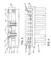
- FIG. 3shows one embodiment of a structure 100 for grounding a silicon active region 102 within a silicon-on-insulator (SOI) substrate 104 .
- SOI substrate 104includes a silicon-on-insulator (SOI) layer 106 and a buried oxide (BOX) layer 108 .
- Silicon active region 102is provided within SOI layer 106 .
- Structure 100includes a bulk silicon substrate 110 having SOI substrate 104 thereover.
- silicon active region 102includes at least one finger element 120 within SOI layer 106 ( FIG. 3 ). In one embodiment, a plurality of finger elements 120 are within SOI layer 106 .
- Each finger element 120is isolated by a shallow trench isolation (STI) region 122 of, for example, silicon dioxide (SiO 2 ).
- STI region 122is not shown in FIG. 3 because it has been replaced by polysilicon ground 130 , as will be described below.
- FIG. 3is viewing FIG. 4 along line 3 - 3 .
- a masking layer 126shown in FIG. 3 of, for example, silicon nitride (Si 3 N 4 ) is shown removed in FIG. 4 (masking layer 126 may be used to form polysilicon ground 130 ).
- a polysilicon ground 130intersects finger element(s) 120 and extends through masking layer 126 , STI region 122 and BOX layer 108 to grounded bulk silicon substrate 110 .
- polysilicon ground 130replaces a part of STI region 122 adjacent to a finger element 120 , if only one is provided, or between adjacent finger elements 120 where a plurality of finger elements 120 are provided.
- Polysilicon ground 130contacts silicon active region 102 and grounded bulk silicon substrate 110 so as to provide a ground path 132 (only one labeled) from silicon active region 102 to grounded bulk silicon substrate 110 .
- Polysilicon ground 130contacts a sidewall 134 of silicon active region 102 , i.e., a sidewall of a finger element 120 .
- silicon active region 102may be advantageously used as part of a VC test structure.
- structure 100may be used in a product chip and positioned for charge dissipation.
- Other regions of silicon active region 128also may use polysilicon ground 130 .
- FIGS. 5 and 6one embodiment of grounding silicon active region 102 within SOI substrate 104 prior to contact dielectric formation will now be described.
- FIGS. 5 and 6also view FIG. 4 along line 3 - 3 .
- SOI substrate 104 including SOI layer 106 and BOX layer 108is provided in any now known or later developed fashion.
- SOI substrate 104is positioned over grounded bulk silicon substrate 110 .
- active silicon region 102 having at least one finger element 120 within SOI layer 106is formed.
- Masking layer 126is used to mask out the desired active silicon region 102 .
- each finger element 120is separated from an adjacent finger element 120 , by STI region 122 .
- finger element(s) 120may be formed by any now known or later developed technique for forming STI region 122 within SOI layer 106 .
- a next stepincludes forming polysilicon ground 130 ( FIG. 3 ) intersecting finger element(s) 120 and extending through STI regions 122 in layer 106 and through BOX layer 108 to grounded bulk silicon substrate 110 .
- Polysilicon ground 130 ( FIG. 3 )contacts silicon active region 102 , via finger element(s) 120 , and grounded bulk silicon substrate 110 .
- this stepmay include forming a mask 140 having an opening 142 substantially orthogonal to plurality of finger elements 120 and STI region 122 ( FIG. 4 ) therebetween.
- etching 146is performed through barrier layer 126 (if provided), STI region 122 ( FIG.
- STI region 122is removed adjacent to a finger element 120 where one is provided, or between at least two of a plurality of finger elements 120 , through BOX layer 108 to grounded bulk silicon substrate 110 to form a ground opening 144 .
- Etching 146may include any now known or later developed chemistries appropriate for the layers being etched.
- opening 142 and hence, ground opening 144is formed as a trench. That is, a ground opening trench would be formed in the areas where polysilicon ground 130 is shown in FIG. 4 such that polysilicon ground 130 includes a polysilicon filled trench.
- a precleanmay be provided.
- a polysiliconis deposited in ground opening 144 ( FIG. 6 ), and the polysilicon is planarized to arrive at structure 100 .
- Active region 102is thus grounded by the time that active region 102 is formed and doped.
- FIGS. 7-8one embodiment of a structure 200 for grounding a gate stack 202 , e.g., of polysilicon, through an SOI substrate 204 will now be described.
- FIG. 8shows structure 200 with most of a barrier layer 226 removed for clarity (not actually).
- SOI substrate 204includes SOI layer 206 and BOX layer 208 .
- Structure 200may also include other test structures 228 and other gate stacks (not shown), which utilize polysilicon ground 230 , described below.
- Structure 200may include bulk silicon substrate 210 having SOI substrate 204 thereover.
- a polysilicon ground 230extends through SOI layer 206 and BOX layer 208 to bulk silicon substrate 210 .
- a polysilicon oxide (SiO 2 ) layer 240is included on an upper surface 242 of polysilicon ground 230 .
- Polysilicon oxide layer 240is insufficiently insulative to prevent electrical conductivity therethrough.
- upper surface 242 of polysilicon ground 230is uneven so as to make polysilicon oxide layer 240 insufficiently insulative to prevent electrical conductivity therethrough.
- the polysilicon of gate stack 202contacts polysilicon oxide layer 240 .
- polysilicon gate oxide layer 240actually forms a part of gate stack 202 . Because polysilicon oxide layer 240 is electrically leaky, it provides a ground path from polysilicon gate stack 202 to grounded bulk silicon substrate 210 . Since structure 200 is present prior to formation of polysilicon gate stack 202 , it may advantageously be used as a part of a VC test structure. In addition, structure 200 may be used in a product chip and positioned for charge dissipation.
- Structure 200may be formed by using a mask to form openings through SOI substrate 204 .
- the openingsare filled with polysilicon, and the surface is polished.
- the polysilicon of polysilicon ground 230grows conformally so that the sides of the polysilicon crystals are exposed to the surface, i.e., the top of the opening.
- This exposed surface 242results in a polysilicon that is more bumpy and uneven than the surface of polysilicon (e.g., polysilicon gate stack 202 ) grown vertically across much of the wafer surface.
- polysilicon oxide layer 240i.e., gate dielectric, grown over this uneven upper surface 242 will be extremely leaky.
- a substantial ground path 250may be created.
- structures 100 , 200may provide a ground path for charge dissipation within product chips during FEOL processing.
- Other applications besides FEOL VC inspectionalso can benefit from the above-described embodiments. For instance, grounding of an active region and/or gate stack levels might be useful to mitigate charge damage from reactive ion etching (RIE) processing.
- RIEreactive ion etching
Landscapes
- Engineering & Computer Science (AREA)
- Physics & Mathematics (AREA)
- Condensed Matter Physics & Semiconductors (AREA)
- General Physics & Mathematics (AREA)
- Manufacturing & Machinery (AREA)
- Computer Hardware Design (AREA)
- Microelectronics & Electronic Packaging (AREA)
- Power Engineering (AREA)
- Semiconductor Integrated Circuits (AREA)
- Thin Film Transistor (AREA)
Abstract
Description
- 1. Technical Field
- The invention relates generally to semiconductor fabrication, and more particularly, to structures and a method for grounding front-end-of-line (FEOL) structures, such as a gate stack or active region, through a silicon-on-insulator (SOI) substrate.
- 2. Background Art
- In-line voltage contrast (VC) inspection is a powerful technique for detecting and isolating yield limiting defects in the semiconductor fabricating industry. In-line VC inspection includes scanning the wafer surface in which test structures exist with a scanning electron microscope (SEM). As the inspection proceeds, the SEM induces a charge on all electrically floating elements whereas any grounded elements remain at a zero potential. This potential difference is visible to the SEM. In particular, for electron landing energies less than the second crossover of the secondary electron yield curve (approximately 1.5 keV for tungsten (W) and copper (Cu)), grounded elements appear bright whereas floating elements appear dark.
- Test structures exploiting this phenomenon can be created for many yield limiting defects including metal, gate and active region shorts and opens, and via and contact opens. For example, FIGS.1A-B, show a short (
FIG. 1B ) indicated by a normally floating (dark) element becoming bright, and an open (FIG. 1A ) indicated when a normally bright element becomes dark. As shown, even if the defect causing the electrical failure is buried or extremely small, its existence is indicated by a change in the VC signal of the entire element. In addition, the exact location of an open is indicated by a change in the VC signal of the structure after the break. - A number of challenges exist relative to building VC test structures. One challenge is grounding front-end-of-line (FEOL) structures targeting the active region or gate stack levels, especially for silicon-on-insulator (SOI) technology. For bulk silicon technology, an active region may be grounded to the substrate by doping the active region P+, while masking out the N well so that the P+ directly contacts the P− material of the substrate. However, with SOI technology, the buried oxide (BOX) layer presents an additional barrier so the above-described grounding technique does not work. Some SOI technologies provide a mask level for forming holes through the BOX layer. Design rules typically do not allow this level and the active region or gate stack levels to be coincident. However, this level enables the first metal level to make contact to the substrate. Since the active region and gate stack levels also can be connected to the first metal level, they may be grounded through as shown in
FIG. 2 . Unfortunately this ground path is not helpful for VC inspection for active region and gate stack structures because the ground path to the VC test structure is required when the test structure is still exposed at the wafer surface and visible to the SEM. Therefore, VC test structures that require grounding of an active region are currently impossible for SOI technology. - Several approaches exist to ground polysilicon structures in SOI substrates. For example, Patterson et al., “Rapid Reduction of Poly-Silicon Electrical D0 using uLoop Test Structures,” Proceedings of ASMC, pp. 266-272, March 2003, describes the use of a modified process flow for generating grounded gate stack VC test structures. This short loop sequence starts with the formation of a 2000 angstrom (Å) silicon dioxide (SiO2) layer. Contact holes are patterned in the silicon dioxide (SiO2). The contacts are opened with an isotropic etch. The gate stack excluding the gate dielectric (e.g., SiO2) is then deposited. Gate stack VC test structures are then formed using the contact holes to ground select elements. This method has a number of disadvantages. First, special short loop wafers are necessary, which creates an additional cost. Second, because the transistors will not work, very little other data can be collected for comparison. Third, the process sequence is not entirely representative of the real process.
- A second technique to ground gate stack structures in SOI technology is to use large capacitors to generate a virtual ground path. This technique also suffers from a number of drawbacks. First, these capacitors are formed with a plate of gate stack over the active region, and take up a large amount of the area (e.g., approximately 25-40% of a test area). Secondly, a large plate of gate stack is often a design rule violation. A third technique for grounding the gate stack level is through the first metal layer, as described earlier. Again, this method is not useful for VC inspection because the ground path to the VC test structures is required when the test structures are still exposed at the wafer surface. By the first metal level, the test structures have been covered by the contact dielectric.
- In view of the foregoing, there is a need in the art for a solution to the problems of the related art.
- Structures and a method are disclosed for grounding gate-stack and/or silicon active region front-end-of-line structures on a silicon-on-insulator (SOI) substrate, which may be used as test structures for VC inspection. In one embodiment, a structure includes a grounded bulk silicon substrate having the SOI substrate thereover, the SOI substrate including a silicon-on-insulator (SOI) layer and a buried oxide (BOX) layer; a silicon active region having at least one finger element within the SOI layer, the at least one finger element isolated by a shallow trench isolation (STI) layer; and a polysilicon ground intersecting the at least one finger element and extending through the STI layer and the BOX layer to the grounded bulk silicon substrate, the polysilicon ground contacting the silicon active region and the grounded bulk silicon substrate.
- A first aspect of the invention provides a structure comprising: a grounded bulk silicon substrate having a silicon-on-insulator (SOI) substrate thereover, the SOI substrate including a silicon-on-insulator (SOI) layer and a buried oxide (BOX) layer; a silicon active region having at least one finger element within the SOI layer, the at least one finger element isolated by a shallow trench isolation (STI) layer; and a polysilicon ground intersecting the at least one finger element and extending through the STI layer and the BOX layer to the grounded bulk silicon substrate, the polysilicon ground contacting the silicon active region and the grounded bulk silicon substrate.
- A second aspect of the invention provides a method of grounding a silicon active region within a silicon-on-insulator (SOI) substrate prior to contact dielectric formation, the method comprising the steps of: providing the SOI substrate including a silicon-on-insulator (SOI) layer and a buried oxide (BOX) layer, the SOI substrate positioned over a grounded bulk silicon substrate; forming the silicon active region having at least one finger element within the SOI layer, the at least one finger element isolated by a shallow trench isolation (STI) layer; and forming a polysilicon ground intersecting the at least one finger element and extending through the STI layer and the BOX layer to the grounded bulk silicon substrate, the polysilicon ground contacting the silicon active region and the grounded bulk silicon substrate.
- A third aspect of the invention provides a structure for grounding a gate stack through a silicon-on-insulator (SOI) substrate, the structure comprising: a bulk silicon substrate having the SOI substrate thereover, the SOI substrate including a silicon-on-insulator (SOI) layer on top of a buried oxide (BOX) layer; a polysilicon ground extending through the SOI layer and the BOX layer to the bulk silicon substrate; and a gate oxide layer of the gate stack on an upper surface of the polysilicon ground, the gate oxide layer being insufficiently insulative to prevent electrical conductivity therethrough, wherein the gate stack contacts the polysilicon oxide layer.
- The illustrative aspects of the present invention are designed to solve the problems herein described and/or other problems not discussed.
- These and other features of this invention will be more readily understood from the following detailed description of the various aspects of the invention taken in conjunction with the accompanying drawings that depict various embodiments of the invention, in which:
FIG. 1 shows images of defects observed using conventional VC inspection.FIG. 2 shows a conventional approach to grounding an active region.FIGS. 3-4 show a first embodiment of a structure according to the invention.FIGS. 5-6 show steps of forming the structure ofFIG. 3 .FIGS. 7 and 8 show a second embodiment of a structure according to the invention.- It is noted that the drawings of the invention are not to scale. The drawings are intended to depict only typical aspects of the invention, and therefore should not be considered as limiting the scope of the invention. In the drawings, like numbering represents like elements between the drawings.
- Turning to the drawings,
FIG. 3 shows one embodiment of astructure 100 for grounding a siliconactive region 102 within a silicon-on-insulator (SOI)substrate 104.SOI substrate 104 includes a silicon-on-insulator (SOI)layer 106 and a buried oxide (BOX)layer 108. Siliconactive region 102 is provided withinSOI layer 106.Structure 100 includes abulk silicon substrate 110 havingSOI substrate 104 thereover. As shown in the top view ofFIG. 4 , siliconactive region 102 includes at least onefinger element 120 within SOI layer106 (FIG. 3 ). In one embodiment, a plurality offinger elements 120 are withinSOI layer 106. Eachfinger element 120 is isolated by a shallow trench isolation (STI)region 122 of, for example, silicon dioxide (SiO2). For example, eachfinger element 120 is separated from anadjacent finger element 120 bySTI region 122.STI region 122 is not shown inFIG. 3 because it has been replaced bypolysilicon ground 130, as will be described below.FIG. 3 is viewingFIG. 4 along line3-3. Amasking layer 126, shown inFIG. 3 of, for example, silicon nitride (Si3N4) is shown removed inFIG. 4 (masking layer 126 may be used to form polysilicon ground130). Apolysilicon ground 130 intersects finger element(s)120 and extends throughmasking layer 126,STI region 122 andBOX layer 108 to groundedbulk silicon substrate 110. In particular,polysilicon ground 130 replaces a part ofSTI region 122 adjacent to afinger element 120, if only one is provided, or betweenadjacent finger elements 120 where a plurality offinger elements 120 are provided.Polysilicon ground 130 contacts siliconactive region 102 and groundedbulk silicon substrate 110 so as to provide a ground path132 (only one labeled) from siliconactive region 102 to groundedbulk silicon substrate 110.Polysilicon ground 130 contacts asidewall 134 of siliconactive region 102, i.e., a sidewall of afinger element 120. As such, siliconactive region 102 may be advantageously used as part of a VC test structure. In addition,structure 100 may be used in a product chip and positioned for charge dissipation. Other regions of siliconactive region 128 also may usepolysilicon ground 130. - Turning to
FIGS. 5 and 6 , one embodiment of grounding siliconactive region 102 withinSOI substrate 104 prior to contact dielectric formation will now be described.FIGS. 5 and 6 also viewFIG. 4 along line3-3. In a first step,SOI substrate 104 includingSOI layer 106 andBOX layer 108 is provided in any now known or later developed fashion.SOI substrate 104 is positioned over groundedbulk silicon substrate 110. Next,active silicon region 102 having at least onefinger element 120 withinSOI layer 106 is formed. Maskinglayer 126 is used to mask out the desiredactive silicon region 102. As noted above, and as shown inFIG. 4 , eachfinger element 120 is separated from anadjacent finger element 120, bySTI region 122. As such, finger element(s)120 may be formed by any now known or later developed technique for formingSTI region 122 withinSOI layer 106. - A next step includes forming polysilicon ground130 (
FIG. 3 ) intersecting finger element(s)120 and extending throughSTI regions 122 inlayer 106 and throughBOX layer 108 to groundedbulk silicon substrate 110. Polysilicon ground130 (FIG. 3 ) contacts siliconactive region 102, via finger element(s)120, and groundedbulk silicon substrate 110. As shown starting inFIGS. 5 and 6 , this step may include forming amask 140 having anopening 142 substantially orthogonal to plurality offinger elements 120 and STI region122 (FIG. 4 ) therebetween. Next, as shown inFIG. 6 , etching146 is performed through barrier layer126 (if provided), STI region122 (FIG. 5 ) andBOX layer 108 to groundedbulk silicon substrate 110 to form a ground opening144. In particular, a portion ofSTI region 122 is removed adjacent to afinger element 120 where one is provided, or between at least two of a plurality offinger elements 120, throughBOX layer 108 to groundedbulk silicon substrate 110 to form a ground opening144. Etching146 may include any now known or later developed chemistries appropriate for the layers being etched. In one embodiment, opening142 and hence, ground opening144, is formed as a trench. That is, a ground opening trench would be formed in the areas wherepolysilicon ground 130 is shown inFIG. 4 such thatpolysilicon ground 130 includes a polysilicon filled trench. After etching146, a preclean may be provided. Next, as shown inFIG. 3 , a polysilicon is deposited in ground opening144 (FIG. 6 ), and the polysilicon is planarized to arrive atstructure 100.Active region 102 is thus grounded by the time thatactive region 102 is formed and doped. - Turning to
FIGS. 7-8 , one embodiment of astructure 200 for grounding agate stack 202, e.g., of polysilicon, through anSOI substrate 204 will now be described.FIG. 8 showsstructure 200 with most of abarrier layer 226 removed for clarity (not actually).SOI substrate 204 includesSOI layer 206 andBOX layer 208.Structure 200 may also includeother test structures 228 and other gate stacks (not shown), which utilizepolysilicon ground 230, described below.Structure 200 may includebulk silicon substrate 210 havingSOI substrate 204 thereover. Apolysilicon ground 230 extends throughSOI layer 206 andBOX layer 208 tobulk silicon substrate 210. A polysilicon oxide (SiO2)layer 240 is included on anupper surface 242 ofpolysilicon ground 230.Polysilicon oxide layer 240 is insufficiently insulative to prevent electrical conductivity therethrough. In one embodiment,upper surface 242 ofpolysilicon ground 230 is uneven so as to makepolysilicon oxide layer 240 insufficiently insulative to prevent electrical conductivity therethrough. The polysilicon ofgate stack 202 contactspolysilicon oxide layer 240. Note, polysilicongate oxide layer 240 actually forms a part ofgate stack 202. Becausepolysilicon oxide layer 240 is electrically leaky, it provides a ground path frompolysilicon gate stack 202 to groundedbulk silicon substrate 210. Sincestructure 200 is present prior to formation ofpolysilicon gate stack 202, it may advantageously be used as a part of a VC test structure. In addition,structure 200 may be used in a product chip and positioned for charge dissipation. Structure 200 may be formed by using a mask to form openings throughSOI substrate 204. The openings are filled with polysilicon, and the surface is polished. However, the polysilicon ofpolysilicon ground 230 grows conformally so that the sides of the polysilicon crystals are exposed to the surface, i.e., the top of the opening. This exposedsurface 242 results in a polysilicon that is more bumpy and uneven than the surface of polysilicon (e.g., polysilicon gate stack202) grown vertically across much of the wafer surface. As a result,polysilicon oxide layer 240, i.e., gate dielectric, grown over this unevenupper surface 242 will be extremely leaky. By generating a large enough area wherepolysilicon gate stack 202 overlaps with masking level, asubstantial ground path 250 may be created.- The above-described method and structures enables in-line VC inspection of gate stack and active regions on full flow wafers using standard processing despite the use of SOI technology. Using the above-described embodiments, VC test structures that require grounded active regions are now possible. The structures require very little area. In addition to in-line VC inspection, as noted above,
structures - The foregoing description of various aspects of the invention has been presented for purposes of illustration and description. It is not intended to be exhaustive or to limit the invention to the precise form disclosed, and obviously, many modifications and variations are possible. Such modifications and variations that may be apparent to a person skilled in the art are intended to be included within the scope of the invention as defined by the accompanying claims.
Claims (20)
Priority Applications (2)
| Application Number | Priority Date | Filing Date | Title |
|---|---|---|---|
| US11/308,408US7518190B2 (en) | 2006-03-22 | 2006-03-22 | Grounding front-end-of-line structures on a SOI substrate |
| US12/348,438US7732866B2 (en) | 2006-03-22 | 2009-01-05 | Grounding front-end-of-line structures on a SOI substrate |
Applications Claiming Priority (1)
| Application Number | Priority Date | Filing Date | Title |
|---|---|---|---|
| US11/308,408US7518190B2 (en) | 2006-03-22 | 2006-03-22 | Grounding front-end-of-line structures on a SOI substrate |
Related Child Applications (1)
| Application Number | Title | Priority Date | Filing Date |
|---|---|---|---|
| US12/348,438ContinuationUS7732866B2 (en) | 2006-03-22 | 2009-01-05 | Grounding front-end-of-line structures on a SOI substrate |
Publications (2)
| Publication Number | Publication Date |
|---|---|
| US20070221990A1true US20070221990A1 (en) | 2007-09-27 |
| US7518190B2 US7518190B2 (en) | 2009-04-14 |
Family
ID=38532452
Family Applications (2)
| Application Number | Title | Priority Date | Filing Date |
|---|---|---|---|
| US11/308,408Active2027-08-09US7518190B2 (en) | 2006-03-22 | 2006-03-22 | Grounding front-end-of-line structures on a SOI substrate |
| US12/348,438Expired - Fee RelatedUS7732866B2 (en) | 2006-03-22 | 2009-01-05 | Grounding front-end-of-line structures on a SOI substrate |
Family Applications After (1)
| Application Number | Title | Priority Date | Filing Date |
|---|---|---|---|
| US12/348,438Expired - Fee RelatedUS7732866B2 (en) | 2006-03-22 | 2009-01-05 | Grounding front-end-of-line structures on a SOI substrate |
Country Status (1)
| Country | Link |
|---|---|
| US (2) | US7518190B2 (en) |
Cited By (8)
| Publication number | Priority date | Publication date | Assignee | Title |
|---|---|---|---|---|
| US20070115606A1 (en)* | 2005-11-21 | 2007-05-24 | Devries Kenneth L | Method and structure for charge dissipation in integrated circuits |
| US20100258720A1 (en)* | 2009-04-08 | 2010-10-14 | Hong Xiao | Test structure for charged particle beam inspection and method for defect determination using the same |
| US20100301331A1 (en)* | 2009-05-26 | 2010-12-02 | International Business Machines Corporation | Body contact structure for in-line voltage contrast detection of pfet silicide encroachment |
| US20110013826A1 (en)* | 2009-04-08 | 2011-01-20 | Hong Xiao | Test structure for charged particle beam inspection and method for defect determination using the same |
| US8750597B2 (en) | 2011-11-23 | 2014-06-10 | International Business Machines Corporation | Robust inspection alignment of semiconductor inspection tools using design information |
| US20160197021A1 (en)* | 2013-12-20 | 2016-07-07 | Renesas Electronics Corporation | Semiconductor device and manufacturing method thereof |
| JP2017208560A (en)* | 2017-07-07 | 2017-11-24 | ルネサスエレクトロニクス株式会社 | Manufacturing method of semiconductor device |
| US20230369337A1 (en)* | 2022-05-16 | 2023-11-16 | Skyworks Solutions, Inc. | Noise reduction in silicon-on-insulator devices |
Families Citing this family (19)
| Publication number | Priority date | Publication date | Assignee | Title |
|---|---|---|---|---|
| US7663192B2 (en)* | 2008-06-30 | 2010-02-16 | Intel Corporation | CMOS device and method of manufacturing same |
| US8350583B2 (en)* | 2009-08-12 | 2013-01-08 | International Business Machines Corporation | Probe-able voltage contrast test structures |
| US8399266B2 (en) | 2011-01-25 | 2013-03-19 | International Business Machines Corporation | Test structure for detection of gap in conductive layer of multilayer gate stack |
| US9780007B2 (en) | 2012-01-04 | 2017-10-03 | Globalfoundries Inc. | LCR test circuit structure for detecting metal gate defect conditions |
| US9799575B2 (en) | 2015-12-16 | 2017-10-24 | Pdf Solutions, Inc. | Integrated circuit containing DOEs of NCEM-enabled fill cells |
| US10199283B1 (en) | 2015-02-03 | 2019-02-05 | Pdf Solutions, Inc. | Method for processing a semiconductor wager using non-contact electrical measurements indicative of a resistance through a stitch, where such measurements are obtained by scanning a pad comprised of at least three parallel conductive stripes using a moving stage with beam deflection to account for motion of the stage |
| US9805994B1 (en) | 2015-02-03 | 2017-10-31 | Pdf Solutions, Inc. | Mesh-style NCEM pads, and process for making semiconductor dies, chips, and wafers using in-line measurements from such pads |
| US10978438B1 (en) | 2015-12-16 | 2021-04-13 | Pdf Solutions, Inc. | IC with test structures and E-beam pads embedded within a contiguous standard cell area |
| US10593604B1 (en) | 2015-12-16 | 2020-03-17 | Pdf Solutions, Inc. | Process for making semiconductor dies, chips, and wafers using in-line measurements obtained from DOEs of NCEM-enabled fill cells |
| US9929063B1 (en) | 2016-04-04 | 2018-03-27 | Pdf Solutions, Inc. | Process for making an integrated circuit that includes NCEM-Enabled, tip-to-side gap-configured fill cells, with NCEM pads formed from at least three conductive stripes positioned between adjacent gates |
| US9627371B1 (en) | 2016-04-04 | 2017-04-18 | Pdf Solutions, Inc. | Integrated circuit containing standard logic cells and library-compatible, NCEM-enabled fill cells, including at least via-open-configured, GATE-short-configured, GATECNT-short-configured, and AA-short-configured, NCEM-enabled fill cells |
| US9905553B1 (en) | 2016-04-04 | 2018-02-27 | Pdf Solutions, Inc. | Integrated circuit containing standard logic cells and library-compatible, NCEM-enabled fill cells, including at least via-open-configured, AACNT-short-configured, GATECNT-short-configured, and metal-short-configured, NCEM-enabled fill cells |
| US9748153B1 (en) | 2017-03-29 | 2017-08-29 | Pdf Solutions, Inc. | Process for making and using a semiconductor wafer containing first and second does of standard cell compatible, NCEM-enabled fill cells, with the first DOE including side-to-side short configured fill cells, and the second DOE including tip-to-side short configure |
| US9773774B1 (en) | 2017-03-30 | 2017-09-26 | Pdf Solutions, Inc. | Process for making and using a semiconductor wafer containing first and second DOEs of standard cell compatible, NCEM-enabled fill cells, with the first DOE including chamfer short configured fill cells, and the second DOE including corner short configured fill cells |
| US9786649B1 (en) | 2017-06-27 | 2017-10-10 | Pdf Solutions, Inc. | Process for making and using a semiconductor wafer containing first and second DOEs of standard cell compatible, NCEM-enabled fill cells, with the first DOE including via open configured fill cells, and the second DOE including stitch open configured fill cells |
| US9768083B1 (en) | 2017-06-27 | 2017-09-19 | Pdf Solutions, Inc. | Process for making and using a semiconductor wafer containing first and second DOEs of standard cell compatible, NCEM-enabled fill cells, with the first DOE including merged-via open configured fill cells, and the second DOE including snake open configured fill cells |
| US10096530B1 (en) | 2017-06-28 | 2018-10-09 | Pdf Solutions, Inc. | Process for making and using a semiconductor wafer containing first and second DOEs of standard cell compatible, NCEM-enabled fill cells, with the first DOE including merged-via open configured fill cells, and the second DOE including stitch open configured fill cells |
| US9865583B1 (en) | 2017-06-28 | 2018-01-09 | Pdf Solutions, Inc. | Process for making and using a semiconductor wafer containing first and second DOEs of standard cell compatible, NCEM-enabled fill cells, with the first DOE including snake open configured fill cells, and the second DOE including stitch open configured fill cells |
| US10546929B2 (en)* | 2017-07-19 | 2020-01-28 | Commissariat A L'energie Atomique Et Aux Energies Alternatives | Optimized double-gate transistors and fabricating process |
Citations (12)
| Publication number | Priority date | Publication date | Assignee | Title |
|---|---|---|---|---|
| US5557135A (en)* | 1991-10-17 | 1996-09-17 | Nippon Steel Semiconductor Corporation | Semiconductor device with field shield isolation structure and a method of manufacturing the same |
| US5959459A (en)* | 1996-12-10 | 1999-09-28 | International Business Machines Corporation | Defect monitor and method for automated contactless inline wafer inspection |
| US6049109A (en)* | 1994-09-14 | 2000-04-11 | Kabushiki Kaisha Toshiba | Silicon on Insulator semiconductor device with increased withstand voltage |
| US6452412B1 (en)* | 1999-03-04 | 2002-09-17 | Advanced Micro Devices, Inc. | Drop-in test structure and methodology for characterizing an integrated circuit process flow and topography |
| US20020151091A1 (en)* | 2001-04-16 | 2002-10-17 | Christopher Shaw | Measuring back-side voltage of an integrated circuit |
| US20030071262A1 (en)* | 2000-08-25 | 2003-04-17 | Kla-Tencor Technologies Corporation | Apparatus and methods for semiconductor IC failure detection |
| US20030098706A1 (en)* | 2001-11-06 | 2003-05-29 | Hans-Ulrich Schroeder | Charge detector semiconductor component, system comprising a charge detector semiconductor component and a reference semiconductor component, wafer, use of a wafer, and method for the qualitative and quantitative measurement of charging of a wafer |
| US20030234430A1 (en)* | 2002-06-20 | 2003-12-25 | International Business Machines Corporation | Method and apparatus to make a semiconductor chip susceptible to radiation failure |
| US6720779B1 (en)* | 2002-07-10 | 2004-04-13 | Kla-Tencor Technologies Corporation | Defect type identification using hyper-extracting-field |
| US6727501B1 (en)* | 2001-09-27 | 2004-04-27 | Kla-Tencor Corporation | Method for detecting over-etch defects |
| US6855568B2 (en)* | 2001-06-29 | 2005-02-15 | Kla-Tencor Corporation | Apparatus and methods for monitoring self-aligned contact arrays using voltage contrast inspection |
| US6861666B1 (en)* | 2001-10-17 | 2005-03-01 | Kla-Tencor Technologies Corporation | Apparatus and methods for determining and localization of failures in test structures using voltage contrast |
- 2006
- 2006-03-22USUS11/308,408patent/US7518190B2/enactiveActive
- 2009
- 2009-01-05USUS12/348,438patent/US7732866B2/ennot_activeExpired - Fee Related
Patent Citations (12)
| Publication number | Priority date | Publication date | Assignee | Title |
|---|---|---|---|---|
| US5557135A (en)* | 1991-10-17 | 1996-09-17 | Nippon Steel Semiconductor Corporation | Semiconductor device with field shield isolation structure and a method of manufacturing the same |
| US6049109A (en)* | 1994-09-14 | 2000-04-11 | Kabushiki Kaisha Toshiba | Silicon on Insulator semiconductor device with increased withstand voltage |
| US5959459A (en)* | 1996-12-10 | 1999-09-28 | International Business Machines Corporation | Defect monitor and method for automated contactless inline wafer inspection |
| US6452412B1 (en)* | 1999-03-04 | 2002-09-17 | Advanced Micro Devices, Inc. | Drop-in test structure and methodology for characterizing an integrated circuit process flow and topography |
| US20030071262A1 (en)* | 2000-08-25 | 2003-04-17 | Kla-Tencor Technologies Corporation | Apparatus and methods for semiconductor IC failure detection |
| US20020151091A1 (en)* | 2001-04-16 | 2002-10-17 | Christopher Shaw | Measuring back-side voltage of an integrated circuit |
| US6855568B2 (en)* | 2001-06-29 | 2005-02-15 | Kla-Tencor Corporation | Apparatus and methods for monitoring self-aligned contact arrays using voltage contrast inspection |
| US6727501B1 (en)* | 2001-09-27 | 2004-04-27 | Kla-Tencor Corporation | Method for detecting over-etch defects |
| US6861666B1 (en)* | 2001-10-17 | 2005-03-01 | Kla-Tencor Technologies Corporation | Apparatus and methods for determining and localization of failures in test structures using voltage contrast |
| US20030098706A1 (en)* | 2001-11-06 | 2003-05-29 | Hans-Ulrich Schroeder | Charge detector semiconductor component, system comprising a charge detector semiconductor component and a reference semiconductor component, wafer, use of a wafer, and method for the qualitative and quantitative measurement of charging of a wafer |
| US20030234430A1 (en)* | 2002-06-20 | 2003-12-25 | International Business Machines Corporation | Method and apparatus to make a semiconductor chip susceptible to radiation failure |
| US6720779B1 (en)* | 2002-07-10 | 2004-04-13 | Kla-Tencor Technologies Corporation | Defect type identification using hyper-extracting-field |
Cited By (17)
| Publication number | Priority date | Publication date | Assignee | Title |
|---|---|---|---|---|
| US20070115606A1 (en)* | 2005-11-21 | 2007-05-24 | Devries Kenneth L | Method and structure for charge dissipation in integrated circuits |
| US7408206B2 (en)* | 2005-11-21 | 2008-08-05 | International Business Machines Corporation | Method and structure for charge dissipation in integrated circuits |
| US20080191309A1 (en)* | 2005-11-21 | 2008-08-14 | Devries Kenneth L | Methods and structure for charge dissipation in integrated circuits |
| US7759173B2 (en) | 2005-11-21 | 2010-07-20 | International Business Machines Corporation | Methods for charge dissipation in integrated circuits |
| US8299463B2 (en)* | 2009-04-08 | 2012-10-30 | Hermes Microvision, Inc. | Test structure for charged particle beam inspection and method for defect determination using the same |
| US20110013826A1 (en)* | 2009-04-08 | 2011-01-20 | Hong Xiao | Test structure for charged particle beam inspection and method for defect determination using the same |
| US20100258720A1 (en)* | 2009-04-08 | 2010-10-14 | Hong Xiao | Test structure for charged particle beam inspection and method for defect determination using the same |
| US8421009B2 (en)* | 2009-04-08 | 2013-04-16 | Hermes Microvision, Inc. | Test structure for charged particle beam inspection and method for defect determination using the same |
| US20100301331A1 (en)* | 2009-05-26 | 2010-12-02 | International Business Machines Corporation | Body contact structure for in-line voltage contrast detection of pfet silicide encroachment |
| US8039837B2 (en) | 2009-05-26 | 2011-10-18 | International Business Machines Corporation | In-line voltage contrast detection of PFET silicide encroachment |
| US8750597B2 (en) | 2011-11-23 | 2014-06-10 | International Business Machines Corporation | Robust inspection alignment of semiconductor inspection tools using design information |
| US20160197021A1 (en)* | 2013-12-20 | 2016-07-07 | Renesas Electronics Corporation | Semiconductor device and manufacturing method thereof |
| US9721857B2 (en)* | 2013-12-20 | 2017-08-01 | Renesas Electronics Corporation | Semiconductor device and manufacturing method thereof |
| US20170287795A1 (en)* | 2013-12-20 | 2017-10-05 | Renesas Electronics Corporation | Semiconductor device and manufacturing method thereof |
| US10103075B2 (en)* | 2013-12-20 | 2018-10-16 | Renesas Electronics Corporation | Semiconductor device and manufacturing method thereof |
| JP2017208560A (en)* | 2017-07-07 | 2017-11-24 | ルネサスエレクトロニクス株式会社 | Manufacturing method of semiconductor device |
| US20230369337A1 (en)* | 2022-05-16 | 2023-11-16 | Skyworks Solutions, Inc. | Noise reduction in silicon-on-insulator devices |
Also Published As
| Publication number | Publication date |
|---|---|
| US20090146211A1 (en) | 2009-06-11 |
| US7732866B2 (en) | 2010-06-08 |
| US7518190B2 (en) | 2009-04-14 |
Similar Documents
| Publication | Publication Date | Title |
|---|---|---|
| US7518190B2 (en) | Grounding front-end-of-line structures on a SOI substrate | |
| US20200251416A1 (en) | Device-Manufacturing Scheme for Increasing the Density of Metal Patterns in Inter-Layer Dielectrics | |
| US10347729B2 (en) | Device for improving performance through gate cut last process | |
| US5915199A (en) | Method for manufacturing a CMOS self-aligned strapped interconnection | |
| US7119005B2 (en) | Semiconductor local interconnect and contact | |
| US8455932B2 (en) | Local interconnect structure self-aligned to gate structure | |
| US7879650B2 (en) | Method of providing protection against charging damage in hybrid orientation transistors | |
| US5977599A (en) | Formation of a metal via using a raised metal plug structure | |
| US6559485B2 (en) | Semiconductor device having a gate insulation film resistant to dielectric breakdown | |
| CN102456617A (en) | Method of forming self-aligned local interconnect and structure formed thereby | |
| US9728456B2 (en) | Interconnect structure including middle of line (MOL) metal layer local interconnect on etch stop layer | |
| CN101621030B (en) | Self-aligned MOS structure with polysilicon contacts | |
| US6859023B2 (en) | Evaluation method for evaluating insulating film, evaluation device therefor and method for manufacturing evaluation device | |
| US20090189223A1 (en) | Complementary Metal Gate Dense Interconnect and Method of Manufacturing | |
| KR20090125247A (en) | Trench Formation in Semiconductor Materials | |
| WO2003107430A1 (en) | Enhanced structure and method for buried local interconnects | |
| US6590265B2 (en) | Semiconductor device with sidewall spacers having minimized area contacts | |
| US7026198B2 (en) | Focused ion beam treatment method and semiconductor device suitable for its implementation | |
| US8507378B2 (en) | Method and structure for self aligned contact for integrated circuits | |
| US10141194B1 (en) | Manufacturing method of semiconductor structure | |
| JPH07321118A (en) | Wiring forming method for semiconductor device |
Legal Events
| Date | Code | Title | Description |
|---|---|---|---|
| AS | Assignment | Owner name:INTERNATIONAL BUSINESS MACHINES CORPORATION, NEW Y Free format text:ASSIGNMENT OF ASSIGNORS INTEREST;ASSIGNORS:COTE, WILLIAM J.;PATTERSON, OLIVER D.;REEL/FRAME:017346/0886 Effective date:20060314 | |
| AS | Assignment | Owner name:INTERNATIONAL BUSINESS MACHINES CORPORATION, NEW Y Free format text:ASSIGNMENT OF ASSIGNORS INTEREST;ASSIGNORS:COTE, WILLIAM J.;PATTERSON, OLIVER D.;REEL/FRAME:017829/0560 Effective date:20060314 | |
| FEPP | Fee payment procedure | Free format text:PAYOR NUMBER ASSIGNED (ORIGINAL EVENT CODE: ASPN); ENTITY STATUS OF PATENT OWNER: LARGE ENTITY | |
| STCF | Information on status: patent grant | Free format text:PATENTED CASE | |
| REMI | Maintenance fee reminder mailed | ||
| FPAY | Fee payment | Year of fee payment:4 | |
| SULP | Surcharge for late payment | ||
| AS | Assignment | Owner name:GLOBALFOUNDRIES U.S. 2 LLC, NEW YORK Free format text:ASSIGNMENT OF ASSIGNORS INTEREST;ASSIGNOR:INTERNATIONAL BUSINESS MACHINES CORPORATION;REEL/FRAME:036550/0001 Effective date:20150629 | |
| AS | Assignment | Owner name:GLOBALFOUNDRIES INC., CAYMAN ISLANDS Free format text:ASSIGNMENT OF ASSIGNORS INTEREST;ASSIGNORS:GLOBALFOUNDRIES U.S. 2 LLC;GLOBALFOUNDRIES U.S. INC.;REEL/FRAME:036779/0001 Effective date:20150910 | |
| FPAY | Fee payment | Year of fee payment:8 | |
| AS | Assignment | Owner name:WILMINGTON TRUST, NATIONAL ASSOCIATION, DELAWARE Free format text:SECURITY AGREEMENT;ASSIGNOR:GLOBALFOUNDRIES INC.;REEL/FRAME:049490/0001 Effective date:20181127 | |
| AS | Assignment | Owner name:GLOBALFOUNDRIES INC., CAYMAN ISLANDS Free format text:RELEASE BY SECURED PARTY;ASSIGNOR:WILMINGTON TRUST, NATIONAL ASSOCIATION;REEL/FRAME:054479/0842 Effective date:20200410 Owner name:TAIWAN SEMICONDUCTOR MANUFACTURING CO., LTD., TAIWAN Free format text:ASSIGNMENT OF ASSIGNORS INTEREST;ASSIGNOR:GLOBALFOUNDRIES INC.;REEL/FRAME:054482/0862 Effective date:20200515 | |
| AS | Assignment | Owner name:GLOBALFOUNDRIES INC., CAYMAN ISLANDS Free format text:RELEASE BY SECURED PARTY;ASSIGNOR:WILMINGTON TRUST, NATIONAL ASSOCIATION;REEL/FRAME:054636/0001 Effective date:20201117 | |
| FEPP | Fee payment procedure | Free format text:11.5 YR SURCHARGE- LATE PMT W/IN 6 MO, LARGE ENTITY (ORIGINAL EVENT CODE: M1556); ENTITY STATUS OF PATENT OWNER: LARGE ENTITY | |
| MAFP | Maintenance fee payment | Free format text:PAYMENT OF MAINTENANCE FEE, 12TH YEAR, LARGE ENTITY (ORIGINAL EVENT CODE: M1553); ENTITY STATUS OF PATENT OWNER: LARGE ENTITY Year of fee payment:12 |