US20070215960A1 - Methods for Fabrication of Positional and Compositionally Controlled Nanostructures on Substrate - Google Patents
Methods for Fabrication of Positional and Compositionally Controlled Nanostructures on SubstrateDownload PDFInfo
- Publication number
- US20070215960A1 US20070215960A1US10/599,106US59910604AUS2007215960A1US 20070215960 A1US20070215960 A1US 20070215960A1US 59910604 AUS59910604 AUS 59910604AUS 2007215960 A1US2007215960 A1US 2007215960A1
- Authority
- US
- United States
- Prior art keywords
- nanostructure
- fabricating
- nanostructure array
- array
- layer
- Prior art date
- Legal status (The legal status is an assumption and is not a legal conclusion. Google has not performed a legal analysis and makes no representation as to the accuracy of the status listed.)
- Granted
Links
Images


Classifications
- H—ELECTRICITY
- H01—ELECTRIC ELEMENTS
- H01L—SEMICONDUCTOR DEVICES NOT COVERED BY CLASS H10
- H01L21/00—Processes or apparatus adapted for the manufacture or treatment of semiconductor or solid state devices or of parts thereof
- H01L21/02—Manufacture or treatment of semiconductor devices or of parts thereof
- H01L21/04—Manufacture or treatment of semiconductor devices or of parts thereof the devices having potential barriers, e.g. a PN junction, depletion layer or carrier concentration layer
- H01L21/18—Manufacture or treatment of semiconductor devices or of parts thereof the devices having potential barriers, e.g. a PN junction, depletion layer or carrier concentration layer the devices having semiconductor bodies comprising elements of Group IV of the Periodic Table or AIIIBV compounds with or without impurities, e.g. doping materials
- H01L21/30—Treatment of semiconductor bodies using processes or apparatus not provided for in groups H01L21/20 - H01L21/26
- H01L21/302—Treatment of semiconductor bodies using processes or apparatus not provided for in groups H01L21/20 - H01L21/26 to change their surface-physical characteristics or shape, e.g. etching, polishing, cutting
- H01L21/306—Chemical or electrical treatment, e.g. electrolytic etching
- H01L21/308—Chemical or electrical treatment, e.g. electrolytic etching using masks
- H01L21/3083—Chemical or electrical treatment, e.g. electrolytic etching using masks characterised by their size, orientation, disposition, behaviour, shape, in horizontal or vertical plane
- H01L21/3086—Chemical or electrical treatment, e.g. electrolytic etching using masks characterised by their size, orientation, disposition, behaviour, shape, in horizontal or vertical plane characterised by the process involved to create the mask, e.g. lift-off masks, sidewalls, or to modify the mask, e.g. pre-treatment, post-treatment
- B—PERFORMING OPERATIONS; TRANSPORTING
- B81—MICROSTRUCTURAL TECHNOLOGY
- B81C—PROCESSES OR APPARATUS SPECIALLY ADAPTED FOR THE MANUFACTURE OR TREATMENT OF MICROSTRUCTURAL DEVICES OR SYSTEMS
- B81C1/00—Manufacture or treatment of devices or systems in or on a substrate
- B81C1/00015—Manufacture or treatment of devices or systems in or on a substrate for manufacturing microsystems
- B81C1/00023—Manufacture or treatment of devices or systems in or on a substrate for manufacturing microsystems without movable or flexible elements
- B81C1/00111—Tips, pillars, i.e. raised structures
- B—PERFORMING OPERATIONS; TRANSPORTING
- B82—NANOTECHNOLOGY
- B82Y—SPECIFIC USES OR APPLICATIONS OF NANOSTRUCTURES; MEASUREMENT OR ANALYSIS OF NANOSTRUCTURES; MANUFACTURE OR TREATMENT OF NANOSTRUCTURES
- B82Y10/00—Nanotechnology for information processing, storage or transmission, e.g. quantum computing or single electron logic
- G—PHYSICS
- G03—PHOTOGRAPHY; CINEMATOGRAPHY; ANALOGOUS TECHNIQUES USING WAVES OTHER THAN OPTICAL WAVES; ELECTROGRAPHY; HOLOGRAPHY
- G03F—PHOTOMECHANICAL PRODUCTION OF TEXTURED OR PATTERNED SURFACES, e.g. FOR PRINTING, FOR PROCESSING OF SEMICONDUCTOR DEVICES; MATERIALS THEREFOR; ORIGINALS THEREFOR; APPARATUS SPECIALLY ADAPTED THEREFOR
- G03F7/00—Photomechanical, e.g. photolithographic, production of textured or patterned surfaces, e.g. printing surfaces; Materials therefor, e.g. comprising photoresists; Apparatus specially adapted therefor
- G03F7/26—Processing photosensitive materials; Apparatus therefor
- G03F7/40—Treatment after imagewise removal, e.g. baking
- H—ELECTRICITY
- H01—ELECTRIC ELEMENTS
- H01L—SEMICONDUCTOR DEVICES NOT COVERED BY CLASS H10
- H01L21/00—Processes or apparatus adapted for the manufacture or treatment of semiconductor or solid state devices or of parts thereof
- H01L21/02—Manufacture or treatment of semiconductor devices or of parts thereof
- H01L21/04—Manufacture or treatment of semiconductor devices or of parts thereof the devices having potential barriers, e.g. a PN junction, depletion layer or carrier concentration layer
- H01L21/18—Manufacture or treatment of semiconductor devices or of parts thereof the devices having potential barriers, e.g. a PN junction, depletion layer or carrier concentration layer the devices having semiconductor bodies comprising elements of Group IV of the Periodic Table or AIIIBV compounds with or without impurities, e.g. doping materials
- H01L21/30—Treatment of semiconductor bodies using processes or apparatus not provided for in groups H01L21/20 - H01L21/26
- H01L21/302—Treatment of semiconductor bodies using processes or apparatus not provided for in groups H01L21/20 - H01L21/26 to change their surface-physical characteristics or shape, e.g. etching, polishing, cutting
- H01L21/306—Chemical or electrical treatment, e.g. electrolytic etching
- H01L21/308—Chemical or electrical treatment, e.g. electrolytic etching using masks
- H01L21/3083—Chemical or electrical treatment, e.g. electrolytic etching using masks characterised by their size, orientation, disposition, behaviour, shape, in horizontal or vertical plane
- H01L21/3088—Process specially adapted to improve the resolution of the mask
- H—ELECTRICITY
- H10—SEMICONDUCTOR DEVICES; ELECTRIC SOLID-STATE DEVICES NOT OTHERWISE PROVIDED FOR
- H10D—INORGANIC ELECTRIC SEMICONDUCTOR DEVICES
- H10D30/00—Field-effect transistors [FET]
- H10D30/01—Manufacture or treatment
- H10D30/021—Manufacture or treatment of FETs having insulated gates [IGFET]
- H10D30/024—Manufacture or treatment of FETs having insulated gates [IGFET] of fin field-effect transistors [FinFET]
- H—ELECTRICITY
- H10—SEMICONDUCTOR DEVICES; ELECTRIC SOLID-STATE DEVICES NOT OTHERWISE PROVIDED FOR
- H10D—INORGANIC ELECTRIC SEMICONDUCTOR DEVICES
- H10D62/00—Semiconductor bodies, or regions thereof, of devices having potential barriers
- H10D62/10—Shapes, relative sizes or dispositions of the regions of the semiconductor bodies; Shapes of the semiconductor bodies
- H10D62/117—Shapes of semiconductor bodies
- H10D62/118—Nanostructure semiconductor bodies
- H10D62/119—Nanowire, nanosheet or nanotube semiconductor bodies
- H10D62/121—Nanowire, nanosheet or nanotube semiconductor bodies oriented parallel to substrates
- H—ELECTRICITY
- H10—SEMICONDUCTOR DEVICES; ELECTRIC SOLID-STATE DEVICES NOT OTHERWISE PROVIDED FOR
- H10D—INORGANIC ELECTRIC SEMICONDUCTOR DEVICES
- H10D62/00—Semiconductor bodies, or regions thereof, of devices having potential barriers
- H10D62/10—Shapes, relative sizes or dispositions of the regions of the semiconductor bodies; Shapes of the semiconductor bodies
- H10D62/117—Shapes of semiconductor bodies
- H10D62/118—Nanostructure semiconductor bodies
- H10D62/119—Nanowire, nanosheet or nanotube semiconductor bodies
- H10D62/122—Nanowire, nanosheet or nanotube semiconductor bodies oriented at angles to substrates, e.g. perpendicular to substrates
- H—ELECTRICITY
- H10—SEMICONDUCTOR DEVICES; ELECTRIC SOLID-STATE DEVICES NOT OTHERWISE PROVIDED FOR
- H10D—INORGANIC ELECTRIC SEMICONDUCTOR DEVICES
- H10D30/00—Field-effect transistors [FET]
- H10D30/60—Insulated-gate field-effect transistors [IGFET]
- H10D30/62—Fin field-effect transistors [FinFET]
Definitions
- the present inventiondescribes methods for patterning a substrate to create a positional and compositionally well defined nanostructures and nanostructure arrays on a wafer scale.
- the patterned nanostructureshave applications in biological and chemical sensing, catalysis, nanocomputing and nanoelectronics.
- Nanostructuresare structures with characteristic dimensions less than 100 nm, i.e. nanoscale. Matters can exhibit size dependent properties at this scale due to physical laws governing microscopic objects, which enable novel applications. Despite their novel property, however, an economic and production worthy method of fabricating nanostructures and nanostructure arrays on substrate and making necessary connections for functional devices has yet to be found.
- top-down and bottom-up approachesMethods for fabricating nanostructures on substrate fall into two categories, top-down and bottom-up approaches.
- Conventional top-down approachessuch as photolithography, electron beam lithography or ion beam lithography involve creating structures by forming and removing unwanted parts of various films. They are prohibitively expensive for forming devices less than 100 nm.
- the resolution of photolithographyalso suffers from the physical limit of the wavelength of the electromagnetic radiation. Although 30 nm resolution has been demonstrated with extremely short electromagnetic radiation, the cost of such a tool is prohibitively expensive.
- Electron beam lithography and ion beam lithographyboast better resolution down to 10 nm, but these methods require the energetic particle beam to visit each spot sequentially and greatly limit the number of devices that can be made in an industrial production environment.
- Imprint lithographyis known in the art whereby a mold with nanostructures is pressed into a thin polymer film on a substrate, which retains the thickness contrast relief pattern after removal of the mold. Further process is then used to transfer the pattern into the whole resist.
- imprint lithographydoes not generate a pattern; it only transfers an existing pattern on the mold.
- another lithography methodis required, preferably electron beam lithography. This limitation makes the mold fabrication very expensive and imprint mold made today has very low surface coverage of nanostructure-patterned area.
- nanoscale building blocksare synthesized initially by chemical methods, then selectively added to (rather than removal from) a substrate, followed by making contacts to make a functional device.
- these approacheshave limitations on the degree of control they can achieve on each stage of the device fabrication and are not suitable for industrial production.
- Nanoscale building blocks that can be chemically synthesizedinclude carbon annotate, nanowire, nanocrystal, nanorod, etc. Most of the synthesis processes produce a multitude of nanoscale products, which have different dimension, composition and shape, therefore, different physical and chemical properties. For example, heterogeneous nanowires synthesized by chemical vapor deposition are shown in Chem. Mater. 2000, v12, p605-607 (Wu, Y. and Yang, P.). To control the diameter, researchers control the diameter of the catalyst used to grow them, which only shifts the center of a broad distribution of the diameters of materials synthesized, as shown in FIG. 2 of Appl. Phys. Lett. 2001, v78, p2214.
- the final step in making nanostructures into a functional deviceusually requires an electrical connection to a signal processing unit.
- the lack of positional control in the bottom-up approach in depositing the nanostructures on the substratemakes the final connection-making step difficult.
- the position of each nanostructurehas to be determined by microscopy methods such as scanning electron microscopy or atomic force microscopy; then electron beam lithography or other serial lithography is used to make the connections.
- preexisting contact structuresare fabricated with top-down methods; nanoscale building blocks are then deposited onto these structures with contacts established by chance.
- a novel methodis invented to produce high-density nanowire arrays, Science, v300, p 112. Although this method eliminated the nanowire synthesis step and the assembly step, since they have control over the nanowire position, it is still not a production-worthy method on the industrial scale.
- the methodrelies on the selective removal of AlGaAs in the AlGaAs/GaAs superlattice, and uses the superlattice as a mold to deposit materials on wafer.
- the area that can be patternedis defined by the superlattice thickness; to grow a superlattice up to 100 ⁇ m is a very time-consuming step. Even so, they can only pattern a 100- ⁇ m area at the most, and thus exhibit a slow throughput process.
- the methodis also limited to produce only straight nanowire patterns, and not any other shapes.
- SITSidewall image transfer
- Imprint lithographycan transfer nanoscale patterns on a large area, but it can not generate patterns.
- Existing methods for fabrication of nanostructures with imprint lithographydepend on electron beam lithography to make the nanoscale patterns in a mold, which can be very expensive for mold with high nanoscale pattern coverage.
- the present inventioncontemplates that nanoscale patterns can be made on a substrate, which can then be used as mold in imprint lithography.
- Nanowire biosensorshave been discussed in the literature, Science 2001, v293, p1289 and Nano Letters, 2004, v4, p51, the content so both are hereby incorporated by reference in its entirety. These sensors are assembled from CVD-synthesized nanowires, and they are difficult to manufacture on an industrial scale. Sensors of the prior art do not have the compositional and positional control over the nanostructures that arrays and sensors made in accordance with the present invention possess. In general, the sensors include nanotubes or nanowires in contact with electrodes, thus forming a circuit for current flow. The sensing occurs when analytes contact the nanotubes or nanowires. Chemical sensors based on TiO 2 nanowire are also reported. The present invention contemplates that nanoscale sensing devices may be manufactured cheaply in mass.
- a method for fabricating positional and compositionally controlled nanostructurescomprises:
- a method for fabricating positional and compositionally controlled arbitrary shape nanostructures on a substratecomprises:
- the above fabrication methodscan create at least one nanoscale pattern, a multiple of patterns, of specific predetermined position, shape and composition, patterns over a large area at high throughput satisfactory for industrial requirement.
- the resultant nanostructure patternsare useful for nanostructure arrays, specifically sensor and catalytic arrays.
- the fabrication process of a nanoscale semiconductor sensor array for detecting analytesis provided, with preferred applications in chemical and biological sensing.
- Two conductive elementsconnect the nanostructures to a signal control and processing unit.
- the conductive elementsare fabricated within the said thin semiconductor layer, see FIG. 5 d ref. num 15 .
- the conductive elementsare formed on the nanostructure using standard lithography, see FIG. 5 f num 19 .
- sections of the nanostructurecan be suspended from the substrate. The said nanostructure semiconductor then can be functionalized with specific molecules for detection of certain molecules.
- the fabrication method of a nanoscale oxide sensor array for detecting analytesis provided, with preferred applications in gas phase sensing.
- a mold with nanostructure featuresis fabricated by the second method, and is pressed against a substrate coated with a polymer resist to transfer pattern. Upon separation, the pattern is transferred all the way through the resist by etching.
- the desired composition of materialsis then deposited on the resist layer.
- nanostructures with desired compositionare left on the substrate.
- a masking materialis deposited on the resist layer. Following the dissolution of the resist layer, the masking material that is left on the semiconductor surface can then be used to transfer the nanostructure pattern into the substrate.
- Two conductive elementscan be made to each of the nanostructures by standard lithography methods.
- a method for detecting analytesis also provided.
- the resistance of each of the sensor elements in the sensor arrays fabricated by the two said methodsis measured before and after exposure of the sensor arrays to a sensing environment. Resistance change of each of the sensor elements is then correlated to the detection of the specific analyte the sensor is designed to measure. Optimizing the sensor design by control of the dimension, shape and composition can lead to detection at very low levels, i.e. and ppt concentrations.
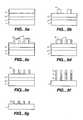
- FIG. 1 a - 1 bis a block diagram for forming an array in accordance with one embodiment of this invention
- FIG. 2is a schematic drawing of a size reduction lithography process in accordance with one embodiment of the present invention.
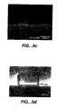
- FIG. 3 ais a SEM of a cross section of an array after thin LTO deposition (44 nm)
- FIG. 3 bis a SEM of a cross section of an array after thick LTO deposition (200 nm).
- FIG. 3 cis a SEM of a cross section of an array after the top LTO layer and poly-Si layer have been etched away from the structure
- FIG. 3 dis a SEM of a cross section after the top LTO layer and poly-Si have been etched away from the structure.
- FIG. 3 eis a SEM cross section of a 20-nm Si nanostructure array made from size reduction lithography
- FIG. 3 fis a SEM to view of the 20-nm Si nanostructure array of FIG. 2 e.
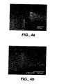
- FIG. 4 ais SEM cross section of a 12-nm Si nanostructure array made after thermal oxide trimming. Inset HRTEM image shows the single crystalline nature of the Si nanowire.
- FIG. 4 bis a SEM cross section of a 7-nm Si nanostructure array made after further thermal oxide trimming.
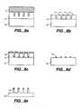
- FIG. 5 a - 5 gis a block diagram of a method in accordance with one embodiment of the present invention.
- FIG. 6 a - 6 dis a block diagram of a method in accordance with one embodiment of the present invention.
- FIG. 6 bshows closed ended nanostructures
- FIG. 6 dshows open ended nanostructures.
- FIG. 7 a - 7 fis a block diagram of a method in accordance with one embodiment of the present invention.
- FIG. 8 a - 8 eis a method in accordance with one embodiment of the present invention utilizing imprint lithography.
- FIG. 9 a - 9 gis a block diagram of a method in accordance with one embodiment of the present invention.
- FIG 10 a - 10 bis a depiction of an array and sensor in accordance with one embodiment of the present invention.
- FIG. 11is a method in accordance with one embodiment of the present invention.
- FIG. 12is a method in accordance with one embodiment of the present invention.
- FIG. 13is a method in accordance with one embodiment of the present invention.
- FIG. 14is a method in accordance with one embodiment of the present invention.
- FIG. 15is a method in accordance with one embodiment of the present invention.
- FIG. 16is a method in accordance with one embodiment of the present invention.
- FIG. 17is a method in accordance with one embodiment of the present invention.
- FIG. 18is a method in accordance with one embodiment of the present invention.
- FIG. 19is a method in accordance with one embodiment of the present invention.
- FIG. 20shows an embodiment of a suspended nanostructure.
- substrateit is meant a layer or layers of materials on which the nanostructure array can be fabricated.
- the substratemay be a single layer of Si, preferably as pure as possible, preferably at least 99.9% pure.
- the substratemay be transparent (as for use in an optoelectronic device) or opaque.
- the thickness of the substrate, whether it is one or multiple layers,is between 500 nm and 1 mm, but this can vary depending on the intended use.
- Siliconis a preferred material for the substrate.
- materialsinclude SiO 2 , Group II-VI and Group III-V semiconductors, any glass or quartz, sapphire, polished metals providing they have an insulating coating.
- the wafer sizemay be any size depending on the manufacturing parameters.
- the substratepreferably has either have an insulator material thereon, or the substrate comprises an insulator, such as SiO 2 , Al 2 O 3 or other insulating material. Oxides are preferred because they are capable of processing at high temperatures.
- the insulating layermay be grown, deposited by any CVD technique, sputtering or evaporation or ion implantation.
- SOIsilicon on insulator
- Thisis a substrate comprising multiple layers, that Si/insulator/Si.
- the top layer and bottom layermay be substituted for other materials as described herein, for the present invention.
- a preferred thickness for SOI substrateis between 500-700 ⁇ m.
- the thickness for the oxide layer here, and for insulator layers used herein in generalranges from between 5 nm to about 100 ⁇ m; preferred thickness is 50 nm to 100 nm.
- the thickness of the single crystal Si layerranges from 0.5 nm to about 500 nm; preferred thickness is 5 nm to 50 nm.
- polysiliconit is meant a contraction of “polycrystalline silicon”.
- forming a nanoscale thin filmit is meant to include the process of providing a substrate and growing, depositing, bonding or otherwise providing materials in the film format.
- the film thicknesscan range from 0.5 nm to 500 nm, preferred thickness is 5 nm to 100 nm.
- the materialscan be conductor, semiconductor or insulator in single crystal, polycrystalline or amorphous state. Preferably, it is single crystal Si. Ge or other semiconducting materials may also be used. Si x Ge 1-x , where 0.01 ⁇ x ⁇ 0.99, where x is mol % are also contemplated. Conducting polymers known in the art are also contemplated.
- the filmcan also comprise more than one layer of materials, with materials for each layer chosen from the above-mentioned materials.
- thin conformal layerit is meant a layer having a thickness from about 1 nm to about 1 ⁇ m, depending on the desired end product. Preferably the thickness is less than about 50 nm.
- Methods for forming a conformal layerinclude, but are not limited to chemical vapor deposition, spin coating or by converting the underlying layer through chemical reaction such as oxidation or nitrification and low pressure chemical vapor deposition, etc.
- nanostructureis meant that at least one, preferably two, of the structure's three dimensions is measured in nanometers.
- the height and width of the nanostructures in accordance with preferred embodiments of the present inventionare between about 0.5 and 100 nm, preferably between 5-50 nm.
- arrayit is meant a substrate having at least one nanostructure thereon.
- anisotropically etchingit is mean removing material with one preferred direction.
- Preferred methods for performing anisotropic etchingare based on plasma etching.
- positional controlledit is meant the ability to fabricate a nanostructure on a substrate and control the placement of the nanostructure within about 20 nm or less.
- the predetermined position for a nanostructureis determined by the selection of any desired specific location on a wafer from any particular or specific point on the nanostructure or nanostructures.
- Positional controlalso means different nanostructures may be fabricated having a specific predetermined location on the wafer with respect to one another or others.
- photolithographyit is meant lithographic techniques using any wavelength, including extreme UV.
- compositionally controlledit is meant that the method of the present invention is capable of fabricating nanostructures having any material, compositions and stoichiometric ratios thereof, including multiple layers vertically.
- the present inventioncontemplates that as many as 100 layer or more can be in 1 nanostructure.
- etching characteristicit is meant etching selectivity
- patternit is meant a design of specific intention that carries with it a specific shape which may include circular, corrugated, elliptical, oblong, oval, parabolic, rectangular and segments or parts of the aforementioned shapes. Complex shapes are also possible, limited only by the imagination.
- the patternmay be continuous or discontinuous.
- the thickness or width of the pattern nanostructuredoes not have to be uniform, but may vary.
- the height of the patternmay change.
- FIG. 3 fshows an example of a pattern in accordance with one embodiment of the present invention.
- detectingit is meant that meaning which is associated in the art with this term, such as observe, find, discover, notice, discover or determine the existence, presence, change or any other condition or state.
- the nanostructureis structurally integral with the top layer. This means, that the top layer is the nanostructure.
- the nanostructurewas made from the top layer of a substrate, for example SOI, where the silicon was the top layer initially, and in the top layer everything but the nanostructure has been etched away.
- insulating layermaterials capable of insulating electrical current flow from the device. Typically, metal oxides are used. Preferred for use in this invention are SiOx, where 0.5 ⁇ x ⁇ 2.
- predetermined positionit is meant that the nanostructures are positioned on the substrate with precision and accuracy.
- the method of the present inventionis capable of positioning a nanostructure on the substrate within at least 20 nm of a predetermined position.
- perovskitesit is meant to include LaFO 3 , SmFeO 3 and
- the present inventioncontemplates controlling the shape of the nanostructures by controlling the shape of the pattern in the mold or by the shape of the pattern in the sacrificial layer.
- the present inventioncontemplates controlling the length of the nanostructures by controlling the length of the pattern in the mold or by the length of the pattern in the sacrificial layer.
- the present inventioncontemplates controlling the position of the nanostructures by controlling the position of the pattern in the mold or by the position of the sacrificial layer.
- Size reduction of nanostructures made in accordance with the present inventionmay be accomplished by producing a 20 nm (silicon, preferred) nanostructure and oxidize it at 800° C. for 20 minutes followed by HF dipping to remove the oxide. This treatment reduced the silicon dimension to ⁇ 12 nm, as shown in FIG. 3 ( a ).
- a high-resolution transmission electron microscopy (HRTEM) imagealso shows the single crystalline nature of the Si nanowire. Further oxidation at 800° C. for 10 minutes reduced the silicon dimension to ⁇ 7 nm, as shown in FIG. 3 ( b ).
- the concave shape of the cross section of Si nanowireis due to lower oxidation rate for concave and convex surfaces (top and bottom) than planar surface (middle).
- the nanostructures of the present inventionare preferably doped. Doping of semiconductors is well known in the art, see for example Cui. et al. J. Phys. Chem. B 104, 5213 (2000), Cui et al. Science 291, 851 (2001) and Duan et al. Nature 409, 66 (2001), the contents of which are hereby incorporated by reference in its entirety. Boron and phosphorus may be doped to provide p-type and n-type materials, respectively. Dopant concentration is controlled depending on the sensitivity desired of the resultant device. Techniques such as epitaxial overgrowth, diffusion, ion implantation are contemplated
- Nanostructureshave a large surface to volume ratio, which make its property sensitive to environmental perturbation on the surface. Especially, current flows through nanostructures within the proximity of the surface, electrical change due to the adsorption or desorption of molecules on the surface can influence the electron flow, which makes nanostructures good sensing devices.
- the present inventioncontemplates that the nanoarrays made in accordance with the present invention are capable of use as chemical and biological sensors and catalytic devices.
- contactsare attached to the nanostructures by standard lithographic techniques.
- the present inventioncontemplates that the in one embodiment the nanosensor described herein has a nanostructure that bridges the gap between two contacts through which electrical current may pass. Sections of the nanostructure may be suspended from the surface. Any changes in the properties of the nanostructure changes the electrical current and the measurement may indicate the presence of an analyte.
- the inventioncontemplates that the analyte may be in any phase, such as solution or gas.
- Arrays according to this inventionare capable of being constructed as a gate-less field effect transistor (FET) by functionalizing the nanostructure array with molecules, compositions or membranes capable of binding (ionically, covalently, van der walls or any other interaction, chemical or physical) with a target molecule of interest. The binding will then result in an increase or decrease in the carriers in the FET structure.
- Sensors constructed in accordance with the method of the present inventionare capable of single molecule detection. Another advantage of sensors in accordance with the present invention is the possibility of dense arrays of nanostructures, which would further increase sensitivity.
- a nanostructure device constructed according to the present inventionmay be made into a sensor device by functionalizing the surface of the nanostructure with a substance capable of responding in some way to the presence of a target molecule.
- the nanostructure array of the present inventionis different from a typical FET because the surface is not covered by a metal gate, but is instead functionalized.
- When the target molecule contacts the functionalized surface of the nanowirea change in nanostructure electrical property (for example, conductance) or optical property occurs.
- the choice of functionalized substance/target molecule for use in accordance with this inventionmay be one well characterized in the art, for example the biotin-streptavidin ligand-receptor relationship.
- photoactive moleculephotonic nanoparticle, inorganic ion, inorganic nanoparticle, magnetic ion, magnetic nanoparticle, electronic nanoparticle, metallic nanoparticle, metal oxide nanoparticle, gold nanoparticle, gold-coated nanoparticle, carbon nanotube, nanocrystal, quantum dot, protein domain, enzyme, hapten, antigen, biotin, digoxygenin, lectin, toxin, radioactive label, fluorophore, chromophore, or chemiluminescent molecule. It is contemplated that any molecule whose presence is a diagnostic of a particular human pathogenic organism, such as bacteria, protozoa, fungi, viruses and prions may be used.
- the sensormay have a biologically and chemically protective coating that will inhibit non-specific interactions of non-targeted analytes.
- Thismay include a surfactant or lipid layer, a polymer layer or a micellar layer.
- the inventionalso contemplates that a multitude of nanosensor arrays in accordance with the present invention may be functionalized with different organics and used to detect an array of molecules in parallel. Thus it is contemplated that one nanostructure is functionalized differently than another nanostructure. There may be 100, or 1000 or more nanostructures functionalized differently.
- Inhibiting materialsmay cover the regions adjacent the nanostructures.
- the inhibiting materialmay be chosen depending on the desired use, but it must be impermeable to at lease one chemical, biochemical or biological target molecule.
- the inhibiting material layermay be impermeable to the target molecule, or semipermeable to the target molecule.
- Electrical contacts to the sensor arraysmay be made in accordance with those methods known in the art, such as electron-beam lithography, ion beam lithography, or photolithography. Suitable materials for the contacts include aluminum, titanium, titanium-tungsten, platinum, gold and copper.
- the nanostructure sensor devicemay be configured to detect electrical signals before and after exposure to an analyte. Changes in signals can be related to detection of the analyte.
- the sensor of the present inventionmay be coupled to a signal control and processing unit.
- FIG 1 ashows the conformal layer structure process as it was transferred into the substrate with further etching.
- This conformal layer structurewas then removed leaving nanostructures/nanostructure arrays of the same material as the substrate.
- the present inventioncontemplates the controlling of the height, width, length, shape, spacing, position, doping level, and/or composition of the nanostructures/ nanostructure arrays.
- Si( 100 )was used as the starting material, this is a preferred embodiment only, and not limiting.
- a 50 ⁇ 70 nm thermal oxide layerwas grown on the Si wafers in a water stream and oxygen at 850° C.
- the optimal thickness of the thermal oxidewas chosen from these two functional considerations.
- the layershould be thick enough to protect the substrate during the removal of the sacrificial polysilicon layer, while a thin layer is desired to minimize pattern broadening when forming the hard mask for subsequent silicon etching.
- a thin layer of polysiliconwas deposited by low-pressure chemical vapor deposition using SiH 4 at 600° C. as the sacrificial layer.
- the layer thicknessis 100 nm for generating Si features with sizes less than 30 nm and 400 nm for larger Si nanostructures.
- the polysilicon layerwas then patterned by photolithography with a GCA 6200 wafer stepper, the resolution of which was around 600 nm. The pattern was transferred from the photoresist layer to the poly-silicon layer by plasma etching in a Lam Research 9400 TCP etcher. The conditions were 50 sccm Cl 2 , 150 sccm HBr, pressure 15 mtorr, electrode temperature 50° C., 300 W top electrode power and 150 W bottom electrode power with a bias of ⁇ 160 V.
- This recipeetched poly-silicon with a speed of ⁇ 7 nm/s and produced a nearly vertical sidewall profile with an angle >89.5°. It is also important to remove the polymers after the polysilicon etching.
- the estimated residue polymer thicknesswas 20 ⁇ 30 nm, which would significantly enlarge the nanometer pattern desired.
- the post etch step for the removal of the polymerwas to dip the wafer in (100:1) HF for 10 s, strip the photoresist with oxygen plasma, followed by (100:1) HF 10 s then piranha [(4:1) H 2 SO 4 : H 2 O 2 ] treated at 120° C.
- Low temperature oxide (LTO)was deposited by low pressure chemical vapor deposition over the patterned polysilicon layer.
- the conditionswere 5 sccm SiH 4 and 70 sccm O 2 at 450° C.
- the deposition ratewas ⁇ 3 nm/min.
- the step coverageis ⁇ 70% for thin films ( ⁇ 50 nm) and ⁇ 60% for thicker films, as shown in FIG. 3 ( a ) and 3 ( b ), respectively.
- the thickness of the deposited LTO on the sidewalldetermines the minimum feature size.
- Anisotropic plasma etchingwas used to remove the LTO on the top of the sacrificial structure and open the polysilicon structure ( FIG. 2 f ).
- the conditionswere: 100 sccm CF 4 , pressure 13 mtorr, 200 W top electrode power and 40 W bottom electrode power with a bias of ⁇ 80 V.
- the etching speedwas ⁇ 2 nm/s for LTO. This recipe also etches polysilicon and single crystal silicon with almost the same speed as for LTO.
- the polysilicon sacrificial layerwas then removed with either wet etching or plasma etching ( FIG. 2 g ). Wet etching was conducted in 1:2 w KOH aqueous solution at 80° C.; the etching speed was around 17 nm/s for poly-silicon and 0.1 nm/s for LTO.
- the polysilicon plasma etching processis the same as the process for transferring pattern from photoresist into polysilicon layer and the etching selectivity of polysilicon to LTO is 22.
- the LTO patternwas then transferred to the thermal oxide layer by plasma etching with conditions 100 sccm CF 4 , pressure 13 mtorr, 200 W top electrode power and 40 W bottom electrode power ( FIG. 2 h ).
- the resulting oxide pattern sidewall profile after this etchingis not ideally vertical, showing some broadening for smaller spacers ( ⁇ 30 nm, FIG. 3 ( c )) and a noticeable undercut for larger spacers (>50 nm, FIG. 3 ( d )).
- the oxide patternwas transferred to silicon by plasma etching with conditions 50 sccm Cl 2 , 150 sccm HBr, pressure 15 mtorr, electrode temperature 50° C., 300 W top electrode power and 150 W bottom electrode power (FIG 2 i ). 20 nm silicon nanostructures can be routinely fabricated with this process, as shown in FIG. 3 ( e ) and FIG. 3 ( f ).
- the resulting 20 nm silicon nanostructurewas oxidized at 800° C. for 20 minutes followed by HF dipping to remove the oxide. This treatment reduced the silicon dimension to ⁇ 12 nm, as shown in FIG. 4 ( a ).
- a high-resolution transmission electron microscopy (HRTEM) imagealso shows the single crystalline nature of the Si nanostructure. Further oxidation at 800° C. for 10 minutes reduced the silicon dimension to ⁇ 7 nm, as shown in FIG. 4 ( b ).
- the concave shape of the cross section of Si nanostructureis due to lower oxidation rate for concave and convex surfaces (top and bottom) than planar surface (middle).
- FIG. 5 ais a cross section view of the basic film stack.
- a nanoscale thin film 2 with desired chemical compositionis formed on top of a substrate 1 , which may comprise an insulating layer for electrical devices.
- a sacrificial layer 4has been deposited on top of an optional protection layer 3 .
- the substrate and nanoscale thin filmare defined above, and the preferred embodiment is SOI wafer.
- the thickness of the nanoscale Si filmcan be reduced further by limited oxidation and removal of the oxidized portion of the film.
- the optional protection layer 3prevents unintended damage or removal of the nanoscale film 2 and it can be formed by but not limited to either physical vapor deposition, chemical vapor deposition or direct growth by oxidation or nitrification of the film 3 .
- the preferred materialis silicon nitride or a silicon oxide, preferably silicon dioxide.
- the sacrificial layer 4is a material that can be removed later by etching; the preferred material is polysilicon or a silicon oxide, preferably silicon dioxide.
- the sacrificial layer 4can be patterned by standard lithography and etching, the pattern of which is shown in FIG. 5 b , which is a cross section view.
- lithography techniques suitable for this inventionare photolithography, electron beam lithography, ion-beam lithography, etc, preferably photolithography.
- Etchingis achieved either in a plasma environment (dry etching) or in a solution environment (wet etching), preferably dry etching.
- a conformal layer 5is then deposited on the fabricated pattern, as in FIG. 5 c , followed by an anisotropic etch to remove all the conformal layer 5 except on the sidewall of sacrificial layer pattern 4 , as depicted in FIG. 5 d .
- the conformal layer 5should have a different etching characteristics than the sacrificial layer 4 so that either material can be selectively removed while remove very little of the other, such material pairs comprise, but not limited to polysilicon and silicon oxide, polysilicon and silicon nitride, silicon oxide and silicon nitride, photoresist and polysilicon, alumina gallium arsenate and gallium arsenate, etc.
- the preferred material pairis polysilicon and a silicon oxide, preferably silicon dioxide.
- FIG. 5Eshows the remaining conformal layer structure 5 has approximately equal width to the film thickness, which can be less than 50 nm.
- This sublithographic imagesthen can be transferred through the protective layer 3 into the desired nanoscale film layer 2 by etching or ion milling, as shown in FIG. 5 f .
- nanostructures with any desired chemical compositionare fabricated in layer 2 , as shown in FIG. 5 g.
- the width of the nanostructurecan be further reduced by either controlled etching or converting to a material that can be selectively removed.
- polymer nanostructurescan be further reduced in size by controlled etching in oxygen plasma.
- Si nanostructurescan be further reduced in size by thermal oxidation to convert to SiO 2 , which then can be removed by HF etching.
- Si nanostructurescan be further reduced in size by controlled XeF 2 etch.
- the position, length and shape of the nanostructuresmay be predetermined by the initial pattern in the sacrificial layer 4 ( FIG. 5 ), but can also be modified after fabrication.
- FIG. 6 ais an example of a 3-D view of two different shapes of patterns created in the sacrificial layer 4 , one is a rectangle, the other is a circle. The shapes are determined by standard lithography, and these specific shapes provided are intended as examples, not as limitations.
- FIG. 6 bshows the shape and position of the nanostructures 2 created on the substrate 1 . The shape of the nanostructure follows the boundary of the sacrificial layer pattern 4 , and the position of the nanostructure is determined by the position of the sacrificial layer pattern 4 .
- the position of the nanostructurecan be predetermined, standard lithography methods, preferably photolithography, can be applied to change the length and/or shape of the nanostructure by masking the desired part with resist 6 and removing the exposed part with etching techniques, as illustrated in FIG. 6 c .
- the present inventioncontemplates the formation of an open ended structure as in FIG. 6 d , a closed ended structure as in FIG. 6 b , or both.
- the present inventioncontemplates controlling the composition of the nanostructures by forming a thin film of desired composition on a substrate. Further, the present invention contemplates controlling the height of the nanostructures by either timed etching into the desired film or the thickness of the desired film. The preferred method is by controlling the thickness of the desired film. The present invention contemplates controlling the width of the nanostructures by either controlling the thickness of the conformal layer or the procedures of after fabrication modification.
- the present inventioncontemplates further modification of shape and length of the nanostructure after fabrication with standard lithography method to remove unwanted parts.
- FIG. 7 ais a cross section view of the basic film stack.
- a sacrificial layer 9has been deposited on top of an optional protection layer 8 on a substrate 7 .
- the substrateis defined above, and the preferred embodiment is Si wafer.
- the optional protection layer 8prevents unintended damage or removal of the substrate 7 and it can be formed by but not limited to either physical vapor deposition, chemical vapor deposition or direct growth by oxidation or nitrification of the substrate 7 .
- the preferred materialis silicon nitride or silicon oxide.
- the sacrificial layer 9is a material that can be removed later by etching; the preferred material is polysilicon or a silicon oxide, preferably silicon dioxide.
- the sacrificial layer 9can be patterned by standard lithography and etching, the pattern of which is shown in FIG. 7 b . Examples of standard lithography are photolithography, electron beam lithography, ion-beam lithography, etc, preferably photolithography. Etching is achieved either in a plasma environment (dry etching) or in a solution environment (wet etching), preferably dry etching. A conformal layer 10 is then deposited on the fabricated pattern, as in FIG.
- the conformal layer 10should have a different etching characteristics than the sacrificial layer 9 so that either material can be selectively removed while remove very little of the other, such material pairs comprise, but not limited to polysilicon and a silicon oxide, preferably silicon dioxide, polysilicon and silicon nitride, a silicon oxide, preferably silicon dioxide and silicon nitride, photoresist and polysilicon, alumina gallium arsenate and gallium arsenate, etc.
- the preferred material pairis polysilicon and a silicon oxide, preferably silicon dioxide.
- FIG. 7 eshows the remaining conformal layer structure 10 has approximately equal width to the film thickness, which can be less than 50 nm.
- This sublithographic imagesthen can be transferred through the protective layer 8 into substrate 7 by etching or ion milling, as shown in FIG. 7 f . After removing of protective layer 8 , nanostructures with desired chemical composition ire fabricated in substrate 7 .
- the width of the nanostructurecan be further reduced by either controlled etching or converting to a material that can be selectively removed.
- Si nanostructurescan be further reduced in size by controlled XeF 2 etch.
- Si nanostructurescan be further reduced in size by thermal oxidation to convert to SiO 2 , which then can be removed by HF etching.
- the position, length and shape of the nanostructuresare determined by the initial pattern n the sacrificial layer 9 , but can also be modified after fabrication, similar to the teaching related to FIG. 6 .
- the nanostructures thus fabricated on the substrate 7can be used as a mold to transfer he nanostructure pattern
- FIGS. 8 a - 8 eillustrate the process of imprint lithography to transfer the pattern onto a substrate.
- FIG. 8 ais a cross section view of a mold thus fabricated by the above method pressed against a substrate 12 coated with a resist 11 . A thickness variation is created in the resist layer 1 .
- an anisotropic etching processis used to transfer the pattern into entire resist, as shown in FIG. 8 b.
- the desired composition of materials or layers of materialsthen can be deposited vertically onto the patterned substrate 12 , preferably by evaporation or sputtering in vacuum environment, as shown in FIG. 8 c .
- the resist 11is removed by dissolution in solvent, which left the deposited material 13 on the substrate 12 , as shown in FIG. 8 d .
- the deposited material 13can also act as a mask to further transfer the nanostructure pattern into substrate 12 , as depicted in FIG. 8 e .
- the present inventioncontemplates controlling the shape of the nanostructures by controlling the shape of the pattern in the mold, which is further controlled in the mold fabrication process by the shape of the pattern in the sacrificial layer.
- the present inventioncontemplates controlling the length of the nanostructures by controlling the length of the pattern in the mold, which is further controlled in the mold fabrication process by the length of the pattern in the sacrificial layer.
- the present inventioncontemplates controlling the position of the nanostructures by controlling the position of the pattern in the mold, which is further controlled in the mold fabrication process by the position of the sacrificial layer.
- FIG. 9 a - 9 gShown in FIG. 9 a - 9 g are examples of methods for the fabrication of nanoscale sensing devices by sidewall image transfer method.
- ( 15 )is the nanoscale thick semiconductor layer;
- ( 16 )is a protective layer;
- ( 17 )is a thin conformal layer;
- ( 18 )is a resist;
- ( 19 )is a contact.
- FIG. 9 gshows an embodiment where the nanostructure is functionalized with a functionalizing agent, R.
- FIG. 10 ashows one embodiment of an array in accordance with the present invention.
- FIG. 10 bshows a sensor device in accordance with one embodiment of the invention
- ( 23 )is an insulator layer;
- ( 24 )is a nanostructure sensing element comprising TiO 2 , SiO 2 , or the like and
- ( 25 )is a contact or conductor.
- Nanostructure/Nanostructure Array SensorsNanostructures/Nanostructure Arrays and Contacts Fabricated in Parallel (at the same time)
- nanostructure arrays and sensors made using the nanoarrayshave contacts that are effectively in intimate contact and contiguous with the top semiconductor layer of the substrate, for example see FIG. 9 d , ( 15 ).
- the top substrate layer, the contact and the nanostructurewould all be of the same semiconductor material, preferably Si.
- Nanostructure array sensors in accordance with the present invention and possession the positional and compositional controlmay be fabricated in the following manner, with reference to FIG. 11 .
- the substrate ( 1 )comprises a multilayer structure of a semiconductor/insulator/semiconductor), an insulating layer ( 2 ) may be deposited.
- a sacrificial layer ( 3 )may then be deposited on top of this insulating layer.
- a photoresist ( 5 )may be spin-cast on top of the sacrificial layer, and a pattern will be generated in the photoresist via photolithography. The photoresist will serve as a mask to pattern the sacrificial layer through etching. Preferably the etch process is stopped at the insulating layer. The photoresist is then removed.
- a conformal layer ( 4 )may be deposited over the patterned sacrificial layer. Referencing FIG. 12 , the top of the conformal layer ( 4 ) may be removed by etching, thus exposing the top of the sacrificial layer pattern, ( 3 ).
- the sacrificial layer patternwill be selectively removed via etching, leaving conformal layer nanostructures, ( 8 ).
- the conformal layer nanostructureswill serve as a mask to etch into the top layer of the substrate. It is noted that after this step, FIG. 12 now omits the insulator layer 2 .
- the conformal layer nanostructureswill then be removed via etching, leaving behind nanostructures of the substrate material.
- FIG. 13there is described another series of photolithography steps to fabricate photoresist structures ( 5 ) on top of portions of the substrate material nanostructures.
- the exposed substrate material nanostructureswill be etched away, followed by removal of the photoresist via etching. This creates a nanostructure having a shape of a half circle. This nanostructure is the top layer of the substrate that was started with. The nanostructure is made from the original top layer and everything but the nanostructure has been etched away.
- substrateis ( 1 ) which comprises a lower layer that may comprise a semiconductor, shown, but other materials are contemplated, an intermediate layer comprising an insulator and a top layer comprising a nanostructure, formed as in Example 7.
- the nanostructureis fitted with contacts by typical lithograpic techniques and functionalized. Nanostructures are created such that depending on the desired species detection, the surface of the substrate material nanostructures will be functionalized with the appropriate material.
- Nanostructure/Nanostructure Array SensorsNanostructures/Nanostructure Arrays and Contacts Fabricated in Series (at the same time)
- nanostructure arrays and sensors made using the arrayshave contacts that effectively are positioned on top of the nanostructure, for example see FIG. 5 f , ( 19 ).
- the top of the substratebe Si and the nanostructure and contact are of a different material.
- These nanostructure/nanostructure array sensorsmay be fabricated in the following manner. Conformal layer nanostructures are produced as recited in Example 7. These structures would be on top of the insulating layer ( 2 ), and are ( 4 ) in FIG. 15 . Referencing FIG. 16 , another series of photolithography steps may be performed to leave behind photoresist structures on top of portions of the conformal layer nanostructures.
- the photoresist structures and the conformal layer nanostructureswill serve as masks to etch into the substrate.
- the photoresist and conformal layer nanostructureswill then be removed via etching. This will produce substrate material nanostructures and substrate material contacts. Ion implantation will be utilized to create high doping areas for the contacts and low doping areas (the nanostructures) for the detection area. This enables the electron flow control between contacts.
- the surface of the substrate material nanostructureswill be functionalized with the appropriate material, FIG. 17 .
- a nanostructure/nanostructure array patternmade by transferring to a different material via imprint lithography.
- the material chosenmay vary depending on the intended use.
- the nanostructure/nanostructure array patternmay be generated as described in any of the above embodiments. This is intended to be used as the mold, FIGS. 18 and 19 (1: mold/mold material; 2:substrate; 3: imprint resist; 4: desired material depending on application).
- a new second substratewas then selected.
- An imprint resistwas spin-casted onto the substrate is the imprint resist.
- the moldwas then pressed into the resist layer of the second substrate at the necessary temperature and pressure.
- the moldwas then separated from the resist layer.
- the residual resist of the second substratewas etched away to expose the substrate.
- the desired materialwas then deposited onto this second substrate, followed by lift-off of the imprint resist.
- a nanostructuremay be created as described in Example 3, FIG. 5 .
- the underlying optional insulator layer in the substrate or the substratecan be selectively removed by wet or dry etching at intended, predetermined positions or locations to create suspended nanostructures.
- Suspended Si nanostructurescan be created by incorporating a SiO 2 layer in the substrate at the start of the fabrication process and removing the underlying SiO 2 layer at desired locations in solutions containing fluorinated agent after the Si nanostructure is fabricated by process shown in Example 3.
- the rest of the locations where SiO 2 is intended to keepare masked by lithography method, preferably photolithography.
- FIG. 20 bshows an embodiment where the nanostructure is “suspended”.
Landscapes
- Engineering & Computer Science (AREA)
- Manufacturing & Machinery (AREA)
- Physics & Mathematics (AREA)
- Chemical & Material Sciences (AREA)
- Microelectronics & Electronic Packaging (AREA)
- General Physics & Mathematics (AREA)
- Nanotechnology (AREA)
- Power Engineering (AREA)
- Computer Hardware Design (AREA)
- Condensed Matter Physics & Semiconductors (AREA)
- Analytical Chemistry (AREA)
- Mathematical Physics (AREA)
- Theoretical Computer Science (AREA)
- Crystallography & Structural Chemistry (AREA)
- Semiconductor Memories (AREA)
- Catalysts (AREA)
- Micromachines (AREA)
Abstract
Description
- This application claims priority to U.S. Ser. No. 60/554,540, filed Mar. 19, 2004 the contents of which are hereby incorporated by reference in its entirety.
- This invention was made during work supported by U.S. Department of Energy under Contract No. DE-AC03-76SF00098. The government has certain rights in this invention.
- 1. Field of the Invention
- The present invention describes methods for patterning a substrate to create a positional and compositionally well defined nanostructures and nanostructure arrays on a wafer scale. The patterned nanostructures have applications in biological and chemical sensing, catalysis, nanocomputing and nanoelectronics.
- 2. Related Art
- Nanostructures are structures with characteristic dimensions less than 100 nm, i.e. nanoscale. Matters can exhibit size dependent properties at this scale due to physical laws governing microscopic objects, which enable novel applications. Despite their novel property, however, an economic and production worthy method of fabricating nanostructures and nanostructure arrays on substrate and making necessary connections for functional devices has yet to be found.
- Methods for fabricating nanostructures on substrate fall into two categories, top-down and bottom-up approaches. Conventional top-down approaches such as photolithography, electron beam lithography or ion beam lithography involve creating structures by forming and removing unwanted parts of various films. They are prohibitively expensive for forming devices less than 100 nm. The resolution of photolithography also suffers from the physical limit of the wavelength of the electromagnetic radiation. Although 30 nm resolution has been demonstrated with extremely short electromagnetic radiation, the cost of such a tool is prohibitively expensive. Electron beam lithography and ion beam lithography boast better resolution down to 10 nm, but these methods require the energetic particle beam to visit each spot sequentially and greatly limit the number of devices that can be made in an industrial production environment.
- Other novel lithography methods have emerged over the years. Direct write approaches use scanning probe microscopy to deposit molecules on or change physical or chemical properties of the substrate in the proximity of the probe. These methods suffer from slow speed and lack of a general applicability to fabricate functional devices, which limit their use for industrial production.
- Imprint lithography is known in the art whereby a mold with nanostructures is pressed into a thin polymer film on a substrate, which retains the thickness contrast relief pattern after removal of the mold. Further process is then used to transfer the pattern into the whole resist. However, imprint lithography does not generate a pattern; it only transfers an existing pattern on the mold. To generate the nanostructure pattern on the mold, another lithography method is required, preferably electron beam lithography. This limitation makes the mold fabrication very expensive and imprint mold made today has very low surface coverage of nanostructure-patterned area.
- In bottom-up approaches, nanoscale building blocks are synthesized initially by chemical methods, then selectively added to (rather than removal from) a substrate, followed by making contacts to make a functional device. However, these approaches have limitations on the degree of control they can achieve on each stage of the device fabrication and are not suitable for industrial production.
- Nanoscale building blocks that can be chemically synthesized include carbon annotate, nanowire, nanocrystal, nanorod, etc. Most of the synthesis processes produce a multitude of nanoscale products, which have different dimension, composition and shape, therefore, different physical and chemical properties. For example, heterogeneous nanowires synthesized by chemical vapor deposition are shown in Chem. Mater. 2000, v12, p605-607 (Wu, Y. and Yang, P.). To control the diameter, researchers control the diameter of the catalyst used to grow them, which only shifts the center of a broad distribution of the diameters of materials synthesized, as shown in
FIG. 2 ofAppl. Phys. Lett.2001, v78, p2214. To dope the nanowires, investigators introduce gases containing the dopant during the synthesis, as inJ. Phys. Chem.2000, v104, p5213. Although no reproducibility is reported, the uniformity of doping is not expected to be good due to the difference in growth rate related to the broad diameter distribution of nanowires. - Assembly of a nanostructure device by depositing building blocks on a substrate for further processing is currently done by liquid assisted methods, such as Langmuir-Blodgett film or fluidic alignment through micromolded channels. They are described inNano Letters,2003, v3, p1255,Science,2001, v291, p630,Science,2001, v291, p851. These prior art methods suffer from the fact that they can not achieve the degree of position control the modern semiconductor industry has down to 0.01 μm, as shown in
FIGS. 2 and 4 ofScience2001, v291, p630, where broken, double, and tilted lines are seen. The positions are not highly controlled. Another drawback for these methods is that it is still experimental and has a difficult time to scale up for production. - The final step in making nanostructures into a functional device usually requires an electrical connection to a signal processing unit. The lack of positional control in the bottom-up approach in depositing the nanostructures on the substrate makes the final connection-making step difficult. Often the position of each nanostructure has to be determined by microscopy methods such as scanning electron microscopy or atomic force microscopy; then electron beam lithography or other serial lithography is used to make the connections. Or alternatively, preexisting contact structures are fabricated with top-down methods; nanoscale building blocks are then deposited onto these structures with contacts established by chance. Although small quantities of samples have been built using these techniques for lab studies, they are not suitable for large-scale manufacturing.
- To address this problem, a novel method is invented to produce high-density nanowire arrays,Science,v300, p 112. Although this method eliminated the nanowire synthesis step and the assembly step, since they have control over the nanowire position, it is still not a production-worthy method on the industrial scale. The method relies on the selective removal of AlGaAs in the AlGaAs/GaAs superlattice, and uses the superlattice as a mold to deposit materials on wafer. The area that can be patterned is defined by the superlattice thickness; to grow a superlattice up to 100 μm is a very time-consuming step. Even so, they can only pattern a 100-μm area at the most, and thus exhibit a slow throughput process. The method is also limited to produce only straight nanowire patterns, and not any other shapes.
- Sidewall image transfer (SIT) was invented by the semiconductor industry in early 1980s to produce sublithography images and spaces for the formation of polysilicon gate in sub-micron range. Briefly, a vertical step is created on a planar substrate, which is covered by conformal deposition of a silicon oxide, preferably silicon dioxide or nitride. The resulting gate length is approximately equal to the thickness of the layer deposited. More details can be found in U.S. Pat. Nos. 4,358,340, 4,419,809, 4,419,810, 5,139,904, and 5,795,830. A more recent application of this method is towards the fabrication of FinFET, as disclosed inIEEE Device Letters,2002, v23, p25 andSolid-State Electronics,2002, v46, p1595, the contents of which are hereby incorporated by reference in its entirety for all purposes.
- Despite its ability to create sublithography patterns, SIT has only been applied to specific materials, namely Si and polysilicon, and to specific devices such as transistors. The minimum feature dimension can be achieved by this method is on the order of 20 nm and thus limits its application in creating nanostructures.
- A need exists for methods that can fabricate positional, compositionally and shape controlled nanostructures and nanostructure arrays on a substrate to enable large-scale manufacturing.
- Imprint lithography can transfer nanoscale patterns on a large area, but it can not generate patterns. Existing methods for fabrication of nanostructures with imprint lithography depend on electron beam lithography to make the nanoscale patterns in a mold, which can be very expensive for mold with high nanoscale pattern coverage. The present invention contemplates that nanoscale patterns can be made on a substrate, which can then be used as mold in imprint lithography.
- Nanowire biosensors have been discussed in the literature,Science2001, v293, p1289 andNano Letters,2004, v4, p51, the content so both are hereby incorporated by reference in its entirety. These sensors are assembled from CVD-synthesized nanowires, and they are difficult to manufacture on an industrial scale. Sensors of the prior art do not have the compositional and positional control over the nanostructures that arrays and sensors made in accordance with the present invention possess. In general, the sensors include nanotubes or nanowires in contact with electrodes, thus forming a circuit for current flow. The sensing occurs when analytes contact the nanotubes or nanowires. Chemical sensors based on TiO2nanowire are also reported. The present invention contemplates that nanoscale sensing devices may be manufactured cheaply in mass.
- In accordance with one aspect of the present invention, a method for fabricating positional and compositionally controlled nanostructures is disclosed. In one embodiment the method comprises:
- (a) forming a nanoscale thin film of desired nanostructure material composition on the substrate and optionally covering it with a protective layer;
- (b) forming a sacrificial layer on top of the protective layer and patterning the sacrificial layer by conventional or advanced lithography;
- (c) depositing a thin conformal layer over the patterned sacrificial structure which has different etching characteristics than the sacrificial layer;
- (d) anisotropically etching the conformal layer to expose the sacrificial layer and removing the sacrificial layer by selective etching;
- (e) transferring the resulting conformal layer structure through the protective layer to the nanoscale thin film of desired material by etching, and removing the remaining conformal layer structure and protective layer;
- (f) depending on application, the resulting nanostructures in the thin film can be further reduced in dimension by controlled etching or converting to a material that has different etching characteristics and removing the material through selective etching;
- (g) depending on application, the shape of the nanostructure can be modified by standard lithography and etching to remove unwanted parts of the above fabricated nanostructures.
- In accordance with another aspect of the invention, a method for fabricating positional and compositionally controlled arbitrary shape nanostructures on a substrate is provided. In one embodiment the method comprises:
- (a) optionally forming a protective layer on a substrate;
- (b) forming a sacrificial layer on top of the protective layer and patterning the sacrificial layer by conventional or advanced lithography;
- (c) depositing a thin conformal layer over the patterned sacrificial structure which has different etching characteristics than the sacrificial layer;
- (d) anisotropically etching the conformal layer to expose the sacrificial layer and removing the sacrificial layer by selective etching;
- (e) transferring the resulting conformal layer structure through the protective layer to the nanoscale thin film of desired material by etching, and removing the remaining conformal layer structure and protective layer;
- (f) depending on application, the resulting nanostructure pattern in substrate can be further reduced in dimension by controlled etching or converting to a material that has different etching characteristics and removing the material through selective etching;
- (h) depending on application, the shape of the nanostructure can be modified by standard lithography and etching to remove unwanted parts of the above fabricated nanostructures.
- (g) the above nanostructure pattern in substrate then can be used as mold in imprint lithography and create positional and compositionally controlled nanostructures by a lift-off process or an etching process, both of which are well-known in semiconductor industry.
- The above fabrication methods, as employed herein, can create at least one nanoscale pattern, a multiple of patterns, of specific predetermined position, shape and composition, patterns over a large area at high throughput satisfactory for industrial requirement. The resultant nanostructure patterns are useful for nanostructure arrays, specifically sensor and catalytic arrays.
- In one embodiment, the fabrication process of a nanoscale semiconductor sensor array for detecting analytes is provided, with preferred applications in chemical and biological sensing. Two conductive elements connect the nanostructures to a signal control and processing unit. In one arrangement, the conductive elements are fabricated within the said thin semiconductor layer, see
FIG. 5 dref.num 15. In another arrangement, the conductive elements are formed on the nanostructure using standard lithography, seeFIG. 5 f num 19. In some arrangements, sections of the nanostructure can be suspended from the substrate. The said nanostructure semiconductor then can be functionalized with specific molecules for detection of certain molecules. - In another embodiment, the fabrication method of a nanoscale oxide sensor array for detecting analytes is provided, with preferred applications in gas phase sensing. A mold with nanostructure features is fabricated by the second method, and is pressed against a substrate coated with a polymer resist to transfer pattern. Upon separation, the pattern is transferred all the way through the resist by etching. In one arrangement, the desired composition of materials is then deposited on the resist layer. When the resist is dissolved in solution, nanostructures with desired composition are left on the substrate. In another arrangement, a masking material is deposited on the resist layer. Following the dissolution of the resist layer, the masking material that is left on the semiconductor surface can then be used to transfer the nanostructure pattern into the substrate. Two conductive elements can be made to each of the nanostructures by standard lithography methods.
- A method for detecting analytes is also provided. The resistance of each of the sensor elements in the sensor arrays fabricated by the two said methods is measured before and after exposure of the sensor arrays to a sensing environment. Resistance change of each of the sensor elements is then correlated to the detection of the specific analyte the sensor is designed to measure. Optimizing the sensor design by control of the dimension, shape and composition can lead to detection at very low levels, i.e. and ppt concentrations.
- Future features and advantages of the present invention will become apparent to those of ordinary skills in the art in view of the detailed description of preferred embodiments below, when considered together with the attached drawings and claims.
FIG. 1 a-1bis a block diagram for forming an array in accordance with one embodiment of this inventionFIG. 2 is a schematic drawing of a size reduction lithography process in accordance with one embodiment of the present invention.FIG. 3 ais a SEM of a cross section of an array after thin LTO deposition (44 nm)FIG. 3 bis a SEM of a cross section of an array after thick LTO deposition (200 nm).FIG. 3 cis a SEM of a cross section of an array after the top LTO layer and poly-Si layer have been etched away from the structureFIG. 3 dis a SEM of a cross section after the top LTO layer and poly-Si have been etched away from the structure.FIG. 3 eis a SEM cross section of a 20-nm Si nanostructure array made from size reduction lithographyFIG. 3 fis a SEM to view of the 20-nm Si nanostructure array ofFIG. 2 e.FIG. 4 ais SEM cross section of a 12-nm Si nanostructure array made after thermal oxide trimming. Inset HRTEM image shows the single crystalline nature of the Si nanowire.FIG. 4 bis a SEM cross section of a 7-nm Si nanostructure array made after further thermal oxide trimming.FIG. 5 a-5gis a block diagram of a method in accordance with one embodiment of the present invention.FIG. 6 a-6dis a block diagram of a method in accordance with one embodiment of the present invention.FIG. 6 bshows closed ended nanostructures,FIG. 6 dshows open ended nanostructures.FIG. 7 a-7fis a block diagram of a method in accordance with one embodiment of the present invention.FIG. 8 a-8eis a method in accordance with one embodiment of the present invention utilizing imprint lithography.FIG. 9 a-9gis a block diagram of a method in accordance with one embodiment of the present invention.- FIG10a-10bis a depiction of an array and sensor in accordance with one embodiment of the present invention.
FIG. 11 is a method in accordance with one embodiment of the present invention.FIG. 12 is a method in accordance with one embodiment of the present invention.FIG. 13 is a method in accordance with one embodiment of the present invention.FIG. 14 is a method in accordance with one embodiment of the present invention.FIG. 15 is a method in accordance with one embodiment of the present invention.FIG. 16 is a method in accordance with one embodiment of the present invention.FIG. 17 is a method in accordance with one embodiment of the present invention.FIG. 18 is a method in accordance with one embodiment of the present invention.FIG. 19 is a method in accordance with one embodiment of the present invention.FIG. 20 shows an embodiment of a suspended nanostructure.- By “substrate” it is meant a layer or layers of materials on which the nanostructure array can be fabricated. The substrate may be a single layer of Si, preferably as pure as possible, preferably at least 99.9% pure. The substrate may be transparent (as for use in an optoelectronic device) or opaque. Generally the thickness of the substrate, whether it is one or multiple layers, is between 500 nm and 1 mm, but this can vary depending on the intended use.
- Silicon is a preferred material for the substrate. However, also contemplated as materials include SiO2, Group II-VI and Group III-V semiconductors, any glass or quartz, sapphire, polished metals providing they have an insulating coating. The wafer size may be any size depending on the manufacturing parameters. For the purpose of fabricating a functional device, it is to be understood that the substrate preferably has either have an insulator material thereon, or the substrate comprises an insulator, such as SiO2, Al2O3or other insulating material. Oxides are preferred because they are capable of processing at high temperatures. The insulating layer may be grown, deposited by any CVD technique, sputtering or evaporation or ion implantation.
- By “SOI” it is meant “silicon on insulator”. This is a substrate comprising multiple layers, that Si/insulator/Si. The top layer and bottom layer may be substituted for other materials as described herein, for the present invention. A preferred thickness for SOI substrate is between 500-700 μm. The thickness for the oxide layer here, and for insulator layers used herein in general ranges from between 5 nm to about 100 μm; preferred thickness is 50 nm to 100 nm. The thickness of the single crystal Si layer ranges from 0.5 nm to about 500 nm; preferred thickness is 5 nm to 50 nm.
- By “polysilicon” it is meant a contraction of “polycrystalline silicon”.
- By “silicon oxide, silicon nitride” it is meant all stoichiometric ratios of the compounds.
- By “forming a nanoscale thin film” it is meant to include the process of providing a substrate and growing, depositing, bonding or otherwise providing materials in the film format. The film thickness can range from 0.5 nm to 500 nm, preferred thickness is 5 nm to 100 nm. The materials can be conductor, semiconductor or insulator in single crystal, polycrystalline or amorphous state. Preferably, it is single crystal Si. Ge or other semiconducting materials may also be used. SixGe1-x, where 0.01≦x≦0.99, where x is mol % are also contemplated. Conducting polymers known in the art are also contemplated. The film can also comprise more than one layer of materials, with materials for each layer chosen from the above-mentioned materials.
- By “thin conformal layer” it is meant a layer having a thickness from about 1 nm to about 1 μm, depending on the desired end product. Preferably the thickness is less than about 50 nm. Methods for forming a conformal layer include, but are not limited to chemical vapor deposition, spin coating or by converting the underlying layer through chemical reaction such as oxidation or nitrification and low pressure chemical vapor deposition, etc.
- By “nanostructure” is meant that at least one, preferably two, of the structure's three dimensions is measured in nanometers. The height and width of the nanostructures in accordance with preferred embodiments of the present invention are between about 0.5 and 100 nm, preferably between 5-50 nm.
- By “array” it is meant a substrate having at least one nanostructure thereon.
- By “anisotropically etching” it is mean removing material with one preferred direction. Preferred methods for performing anisotropic etching are based on plasma etching.
- By “positional controlled” it is meant the ability to fabricate a nanostructure on a substrate and control the placement of the nanostructure within about 20 nm or less. The predetermined position for a nanostructure is determined by the selection of any desired specific location on a wafer from any particular or specific point on the nanostructure or nanostructures. Positional control also means different nanostructures may be fabricated having a specific predetermined location on the wafer with respect to one another or others.
- By “photolithography” it is meant lithographic techniques using any wavelength, including extreme UV.
- By “compositionally controlled” it is meant that the method of the present invention is capable of fabricating nanostructures having any material, compositions and stoichiometric ratios thereof, including multiple layers vertically. The present invention contemplates that as many as 100 layer or more can be in 1 nanostructure.
- By “etching characteristic” it is meant etching selectivity.
- By “pattern” it is meant a design of specific intention that carries with it a specific shape which may include circular, corrugated, elliptical, oblong, oval, parabolic, rectangular and segments or parts of the aforementioned shapes. Complex shapes are also possible, limited only by the imagination. The pattern may be continuous or discontinuous. The thickness or width of the pattern nanostructure does not have to be uniform, but may vary. The height of the pattern may change.
FIG. 3 fshows an example of a pattern in accordance with one embodiment of the present invention. - By “detecting” it is meant that meaning which is associated in the art with this term, such as observe, find, discover, notice, discover or determine the existence, presence, change or any other condition or state.
- By “at least one nanostructure in the top layer” it is meant that the nanostructure is structurally integral with the top layer. This means, that the top layer is the nanostructure. The nanostructure was made from the top layer of a substrate, for example SOI, where the silicon was the top layer initially, and in the top layer everything but the nanostructure has been etched away.
- By “insulating layer” it is meant materials capable of insulating electrical current flow from the device. Typically, metal oxides are used. Preferred for use in this invention are SiOx, where 0.5≦x≦2.
- By “predetermined position” it is meant that the nanostructures are positioned on the substrate with precision and accuracy. The method of the present invention is capable of positioning a nanostructure on the substrate within at least 20 nm of a predetermined position.
- By “perovskites” it is meant to include LaFO3, SmFeO3and
- The present invention contemplates controlling the shape of the nanostructures by controlling the shape of the pattern in the mold or by the shape of the pattern in the sacrificial layer.
- The present invention contemplates controlling the length of the nanostructures by controlling the length of the pattern in the mold or by the length of the pattern in the sacrificial layer.
- The present invention contemplates controlling the position of the nanostructures by controlling the position of the pattern in the mold or by the position of the sacrificial layer.
- Size reduction of nanostructures made in accordance with the present invention may be accomplished by producing a 20 nm (silicon, preferred) nanostructure and oxidize it at 800° C. for 20 minutes followed by HF dipping to remove the oxide. This treatment reduced the silicon dimension to ˜12 nm, as shown in
FIG. 3 (a). A high-resolution transmission electron microscopy (HRTEM) image also shows the single crystalline nature of the Si nanowire. Further oxidation at 800° C. for 10 minutes reduced the silicon dimension to ˜7 nm, as shown inFIG. 3 (b). The concave shape of the cross section of Si nanowire is due to lower oxidation rate for concave and convex surfaces (top and bottom) than planar surface (middle). - The nanostructures of the present invention are preferably doped. Doping of semiconductors is well known in the art, see for example Cui. et al.J. Phys. Chem.B 104, 5213 (2000), Cui et al.Science291, 851 (2001) and Duan et al.Nature409, 66 (2001), the contents of which are hereby incorporated by reference in its entirety. Boron and phosphorus may be doped to provide p-type and n-type materials, respectively. Dopant concentration is controlled depending on the sensitivity desired of the resultant device. Techniques such as epitaxial overgrowth, diffusion, ion implantation are contemplated
- Nanostructures have a large surface to volume ratio, which make its property sensitive to environmental perturbation on the surface. Especially, current flows through nanostructures within the proximity of the surface, electrical change due to the adsorption or desorption of molecules on the surface can influence the electron flow, which makes nanostructures good sensing devices.
- The present invention contemplates that the nanoarrays made in accordance with the present invention are capable of use as chemical and biological sensors and catalytic devices. In one embodiment of the present invention contacts are attached to the nanostructures by standard lithographic techniques. The present invention contemplates that the in one embodiment the nanosensor described herein has a nanostructure that bridges the gap between two contacts through which electrical current may pass. Sections of the nanostructure may be suspended from the surface. Any changes in the properties of the nanostructure changes the electrical current and the measurement may indicate the presence of an analyte. The invention contemplates that the analyte may be in any phase, such as solution or gas. Arrays according to this invention are capable of being constructed as a gate-less field effect transistor (FET) by functionalizing the nanostructure array with molecules, compositions or membranes capable of binding (ionically, covalently, van der walls or any other interaction, chemical or physical) with a target molecule of interest. The binding will then result in an increase or decrease in the carriers in the FET structure. Sensors constructed in accordance with the method of the present invention are capable of single molecule detection. Another advantage of sensors in accordance with the present invention is the possibility of dense arrays of nanostructures, which would further increase sensitivity.
- A nanostructure device constructed according to the present invention may be made into a sensor device by functionalizing the surface of the nanostructure with a substance capable of responding in some way to the presence of a target molecule. The nanostructure array of the present invention is different from a typical FET because the surface is not covered by a metal gate, but is instead functionalized. When the target molecule contacts the functionalized surface of the nanowire a change in nanostructure electrical property (for example, conductance) or optical property occurs. The choice of functionalized substance/target molecule for use in accordance with this invention may be one well characterized in the art, for example the biotin-streptavidin ligand-receptor relationship. Other materials known in the art are also suitable as functionalized receptors or ligands for target molecules or analytes are calmodulin for sensing Ca2+ions. Single stranded DNAs, antibodies, proteins are all contemplated as suitable for use as as functionalizing molecules. Other possibilities are any photoactive molecule, photonic nanoparticle, inorganic ion, inorganic nanoparticle, magnetic ion, magnetic nanoparticle, electronic nanoparticle, metallic nanoparticle, metal oxide nanoparticle, gold nanoparticle, gold-coated nanoparticle, carbon nanotube, nanocrystal, quantum dot, protein domain, enzyme, hapten, antigen, biotin, digoxygenin, lectin, toxin, radioactive label, fluorophore, chromophore, or chemiluminescent molecule. It is contemplated that any molecule whose presence is a diagnostic of a particular human pathogenic organism, such as bacteria, protozoa, fungi, viruses and prions may be used.
- The sensor may have a biologically and chemically protective coating that will inhibit non-specific interactions of non-targeted analytes. This may include a surfactant or lipid layer, a polymer layer or a micellar layer.
- The invention also contemplates that a multitude of nanosensor arrays in accordance with the present invention may be functionalized with different organics and used to detect an array of molecules in parallel. Thus it is contemplated that one nanostructure is functionalized differently than another nanostructure. There may be 100, or 1000 or more nanostructures functionalized differently.
- Inhibiting materials may cover the regions adjacent the nanostructures. The inhibiting material may be chosen depending on the desired use, but it must be impermeable to at lease one chemical, biochemical or biological target molecule. The inhibiting material layer may be impermeable to the target molecule, or semipermeable to the target molecule.
- Electrical contacts to the sensor arrays may be made in accordance with those methods known in the art, such as electron-beam lithography, ion beam lithography, or photolithography. Suitable materials for the contacts include aluminum, titanium, titanium-tungsten, platinum, gold and copper.
- The nanostructure sensor device may be configured to detect electrical signals before and after exposure to an analyte. Changes in signals can be related to detection of the analyte. Thus the sensor of the present invention may be coupled to a signal control and processing unit.
- The drawings and figures used to describe the present invention are not necessarily to scale.
- The following examples describe and illustrate aspects and features of specific implementations in accordance with the present invention. It should be understood the following is representative only, and that the invention is not limited by the detail set forth in these examples.
- The fabrication of one embodiment of the nanostructures/nanostructure arrays in accordance with the present invention is described below. Referencing FIG1aand FIG1b, a substrate (1) is provided. On top of which a sacrificial layer is deposited, (2). Via lithography, the sacrificial layer was patterned. A thin conformal layer (3) was then deposited on top of the patterned sacrificial layer. The conformal layer was anisotropically etched to expose the sacrificial layer. The sacrificial layer was then selectively removed. FIG1ashows the conformal layer structure process as it was transferred into the substrate with further etching. This conformal layer structure was then removed leaving nanostructures/nanostructure arrays of the same material as the substrate. The present invention contemplates the controlling of the height, width, length, shape, spacing, position, doping level, and/or composition of the nanostructures/ nanostructure arrays.
- Referencing
FIG. 2 : Si(100) was used as the starting material, this is a preferred embodiment only, and not limiting. A 50˜70 nm thermal oxide layer was grown on the Si wafers in a water stream and oxygen at 850° C. The optimal thickness of the thermal oxide was chosen from these two functional considerations. The layer should be thick enough to protect the substrate during the removal of the sacrificial polysilicon layer, while a thin layer is desired to minimize pattern broadening when forming the hard mask for subsequent silicon etching. A thin layer of polysilicon was deposited by low-pressure chemical vapor deposition using SiH4at 600° C. as the sacrificial layer. For improved mechanical stability, the layer thickness is 100 nm for generating Si features with sizes less than 30 nm and 400 nm for larger Si nanostructures. The polysilicon layer was then patterned by photolithography with a GCA 6200 wafer stepper, the resolution of which was around 600 nm. The pattern was transferred from the photoresist layer to the poly-silicon layer by plasma etching in a Lam Research 9400 TCP etcher. The conditions were 50 sccm Cl2, 150 sccm HBr,pressure 15 mtorr, electrode temperature 50° C., 300 W top electrode power and 150 W bottom electrode power with a bias of −160 V. This recipe etched poly-silicon with a speed of ˜7 nm/s and produced a nearly vertical sidewall profile with an angle >89.5°. It is also important to remove the polymers after the polysilicon etching. The estimated residue polymer thickness was 20˜30 nm, which would significantly enlarge the nanometer pattern desired. The post etch step for the removal of the polymer was to dip the wafer in (100:1) HF for 10 s, strip the photoresist with oxygen plasma, followed by (100:1) HF 10 s then piranha [(4:1) H2SO4: H2O2] treated at 120° C. Low temperature oxide (LTO) was deposited by low pressure chemical vapor deposition over the patterned polysilicon layer. The conditions were 5 sccm SiH4and 70 sccm O2at 450° C. The deposition rate was ˜3 nm/min. The step coverage is ˜70% for thin films (<50 nm) and ˜60% for thicker films, as shown inFIG. 3 (a) and3(b), respectively. The thickness of the deposited LTO on the sidewall determines the minimum feature size. Anisotropic plasma etching was used to remove the LTO on the top of the sacrificial structure and open the polysilicon structure (FIG. 2 f). The conditions were: 100 sccm CF4,pressure 13 mtorr, 200 W top electrode power and 40 W bottom electrode power with a bias of −80 V. The etching speed was ˜2 nm/s for LTO. This recipe also etches polysilicon and single crystal silicon with almost the same speed as for LTO. The polysilicon sacrificial layer was then removed with either wet etching or plasma etching (FIG. 2 g). Wet etching was conducted in 1:2wKOH aqueous solution at 80° C.; the etching speed was around 17 nm/s for poly-silicon and 0.1 nm/s for LTO. Due to the etching non-uniformity, the complete removal of poly-silicon is generally not achieved until 2 minutes and this will severely undercuts the LTO spacer at 10 nm scale. Therefore, wet etching is not used for spacers smaller than 30 nm and plasma etching is used instead. The polysilicon plasma etching process is the same as the process for transferring pattern from photoresist into polysilicon layer and the etching selectivity of polysilicon to LTO is 22. The LTO pattern was then transferred to the thermal oxide layer by plasma etching withconditions 100 sccm CF4,pressure 13 mtorr, 200 W top electrode power and 40 W bottom electrode power (FIG. 2 h). The resulting oxide pattern sidewall profile after this etching is not ideally vertical, showing some broadening for smaller spacers (<30 nm,FIG. 3 (c)) and a noticeable undercut for larger spacers (>50 nm,FIG. 3 (d)). The oxide pattern was transferred to silicon by plasma etching with conditions 50 sccm Cl2, 150 sccm HBr,pressure 15 mtorr, electrode temperature 50° C., 300 W top electrode power and 150 W bottom electrode power (FIG2i). 20 nm silicon nanostructures can be routinely fabricated with this process, as shown inFIG. 3 (e) andFIG. 3 (f). - To reduce the silicon size further, the resulting 20 nm silicon nanostructure was oxidized at 800° C. for 20 minutes followed by HF dipping to remove the oxide. This treatment reduced the silicon dimension to ˜12 nm, as shown in
FIG. 4 (a). A high-resolution transmission electron microscopy (HRTEM) image also shows the single crystalline nature of the Si nanostructure. Further oxidation at 800° C. for 10 minutes reduced the silicon dimension to ˜7 nm, as shown inFIG. 4 (b). The concave shape of the cross section of Si nanostructure is due to lower oxidation rate for concave and convex surfaces (top and bottom) than planar surface (middle). - Referring now to
FIG. 5 a-5fwhere one embodiment in accordance with the present invention where fabricating a controlled nanostructure is illustrated.FIG. 5 ais a cross section view of the basic film stack. A nanoscalethin film 2 with desired chemical composition is formed on top of asubstrate 1, which may comprise an insulating layer for electrical devices. Asacrificial layer 4 has been deposited on top of anoptional protection layer 3. The substrate and nanoscale thin film are defined above, and the preferred embodiment is SOI wafer. The thickness of the nanoscale Si film can be reduced further by limited oxidation and removal of the oxidized portion of the film. Theoptional protection layer 3 prevents unintended damage or removal of thenanoscale film 2 and it can be formed by but not limited to either physical vapor deposition, chemical vapor deposition or direct growth by oxidation or nitrification of thefilm 3. The preferred material is silicon nitride or a silicon oxide, preferably silicon dioxide. Thesacrificial layer 4 is a material that can be removed later by etching; the preferred material is polysilicon or a silicon oxide, preferably silicon dioxide. Thesacrificial layer 4 can be patterned by standard lithography and etching, the pattern of which is shown inFIG. 5 b, which is a cross section view. Examples of lithography techniques suitable for this invention are photolithography, electron beam lithography, ion-beam lithography, etc, preferably photolithography. Etching is achieved either in a plasma environment (dry etching) or in a solution environment (wet etching), preferably dry etching. Aconformal layer 5 is then deposited on the fabricated pattern, as in FIG.5c, followed by an anisotropic etch to remove all theconformal layer 5 except on the sidewall ofsacrificial layer pattern 4, as depicted inFIG. 5 d. Theconformal layer 5 should have a different etching characteristics than thesacrificial layer 4 so that either material can be selectively removed while remove very little of the other, such material pairs comprise, but not limited to polysilicon and silicon oxide, polysilicon and silicon nitride, silicon oxide and silicon nitride, photoresist and polysilicon, alumina gallium arsenate and gallium arsenate, etc. The preferred material pair is polysilicon and a silicon oxide, preferably silicon dioxide. - Once the
sacrificial layer 4 is exposed, it can be selectively removed by either dry or wet etching.FIG. 5E shows the remainingconformal layer structure 5 has approximately equal width to the film thickness, which can be less than 50 nm. This sublithographic images then can be transferred through theprotective layer 3 into the desirednanoscale film layer 2 by etching or ion milling, as shown inFIG. 5 f. After removal of theprotective layer 3, nanostructures with any desired chemical composition are fabricated inlayer 2, as shown inFIG. 5 g. - The present invention contemplates that the width of the nanostructure can be further reduced by either controlled etching or converting to a material that can be selectively removed. In one embodiment of the present invention, polymer nanostructures can be further reduced in size by controlled etching in oxygen plasma. In another embodiment of the present invention, Si nanostructures can be further reduced in size by thermal oxidation to convert to SiO2, which then can be removed by HF etching. In another embodiment of the present invention, Si nanostructures can be further reduced in size by controlled XeF2etch.
- The position, length and shape of the nanostructures may be predetermined by the initial pattern in the sacrificial layer4 (
FIG. 5 ), but can also be modified after fabrication.FIG. 6 ais an example of a 3-D view of two different shapes of patterns created in thesacrificial layer 4, one is a rectangle, the other is a circle. The shapes are determined by standard lithography, and these specific shapes provided are intended as examples, not as limitations.FIG. 6 bshows the shape and position of thenanostructures 2 created on thesubstrate 1. The shape of the nanostructure follows the boundary of thesacrificial layer pattern 4, and the position of the nanostructure is determined by the position of thesacrificial layer pattern 4. - Since the position of the nanostructure can be predetermined, standard lithography methods, preferably photolithography, can be applied to change the length and/or shape of the nanostructure by masking the desired part with resist6 and removing the exposed part with etching techniques, as illustrated in
FIG. 6 c. In one embodiment contemplated by the present invention, one can mask half of the structure off and remove the other half. This will result in the fabrication of half circle and half of the rectangle on thesubstrate 1, shown in FIG6d.Accordingly any complex shape can be accomplished. - The present invention contemplates the formation of an open ended structure as in
FIG. 6 d, a closed ended structure as inFIG. 6 b, or both. - Following the teaching of the method, one can readily appreciate that the present invention contemplates controlling the composition of the nanostructures by forming a thin film of desired composition on a substrate. Further, the present invention contemplates controlling the height of the nanostructures by either timed etching into the desired film or the thickness of the desired film. The preferred method is by controlling the thickness of the desired film. The present invention contemplates controlling the width of the nanostructures by either controlling the thickness of the conformal layer or the procedures of after fabrication modification.
- The present invention contemplates further modification of shape and length of the nanostructure after fabrication with standard lithography method to remove unwanted parts.
- Referring now to
FIGS. 7 and 8 , where other embodiments in accordance with the present invention whereby a method of fabricating controlled nanostructure is illustrated.FIG. 7 ais a cross section view of the basic film stack. Asacrificial layer 9 has been deposited on top of anoptional protection layer 8 on asubstrate 7. The substrate is defined above, and the preferred embodiment is Si wafer. Theoptional protection layer 8 prevents unintended damage or removal of thesubstrate 7 and it can be formed by but not limited to either physical vapor deposition, chemical vapor deposition or direct growth by oxidation or nitrification of thesubstrate 7. The preferred material is silicon nitride or silicon oxide. Thesacrificial layer 9 is a material that can be removed later by etching; the preferred material is polysilicon or a silicon oxide, preferably silicon dioxide. Thesacrificial layer 9 can be patterned by standard lithography and etching, the pattern of which is shown inFIG. 7 b. Examples of standard lithography are photolithography, electron beam lithography, ion-beam lithography, etc, preferably photolithography. Etching is achieved either in a plasma environment (dry etching) or in a solution environment (wet etching), preferably dry etching. Aconformal layer 10 is then deposited on the fabricated pattern, as inFIG. 7 c, followed by an anisotropic etch to remove all theconformal layer 10 except on the sidewall ofsacrificial layer pattern 9, as depicted inFIG. 7 d. Theconformal layer 10 should have a different etching characteristics than thesacrificial layer 9 so that either material can be selectively removed while remove very little of the other, such material pairs comprise, but not limited to polysilicon and a silicon oxide, preferably silicon dioxide, polysilicon and silicon nitride, a silicon oxide, preferably silicon dioxide and silicon nitride, photoresist and polysilicon, alumina gallium arsenate and gallium arsenate, etc. The preferred material pair is polysilicon and a silicon oxide, preferably silicon dioxide. - Once the
sacrificial layer 9 is exposed, it can be selectively removed by either dry or wet etching.FIG. 7 eshows the remainingconformal layer structure 10 has approximately equal width to the film thickness, which can be less than 50 nm. This sublithographic images then can be transferred through theprotective layer 8 intosubstrate 7 by etching or ion milling, as shown inFIG. 7 f. After removing ofprotective layer 8, nanostructures with desired chemical composition ire fabricated insubstrate 7. - The width of the nanostructure can be further reduced by either controlled etching or converting to a material that can be selectively removed. In one embodiment of the present invention, Si nanostructures can be further reduced in size by controlled XeF2etch. In one embodiment of the present invention, Si nanostructures can be further reduced in size by thermal oxidation to convert to SiO2, which then can be removed by HF etching.
- The position, length and shape of the nanostructures are determined by the initial pattern n the
sacrificial layer 9, but can also be modified after fabrication, similar to the teaching related toFIG. 6 . The nanostructures thus fabricated on thesubstrate 7 can be used as a mold to transfer he nanostructure pattern FIGS. 8 a-8eillustrate the process of imprint lithography to transfer the pattern onto a substrate.FIG. 8 ais a cross section view of a mold thus fabricated by the above method pressed against asubstrate 12 coated with a resist11. A thickness variation is created in the resistlayer 1. Upon separation, an anisotropic etching process is used to transfer the pattern into entire resist, as shown inFIG. 8 b.The desired composition of materials or layers of materials then can be deposited vertically onto the patternedsubstrate 12, preferably by evaporation or sputtering in vacuum environment, as shown inFIG. 8 c. In the next step, the resist11 is removed by dissolution in solvent, which left the depositedmaterial 13 on thesubstrate 12, as shown inFIG. 8 d. The depositedmaterial 13 can also act as a mask to further transfer the nanostructure pattern intosubstrate 12, as depicted inFIG. 8 e. The present invention contemplates controlling the shape of the nanostructures by controlling the shape of the pattern in the mold, which is further controlled in the mold fabrication process by the shape of the pattern in the sacrificial layer.- The present invention contemplates controlling the length of the nanostructures by controlling the length of the pattern in the mold, which is further controlled in the mold fabrication process by the length of the pattern in the sacrificial layer.
- The present invention contemplates controlling the position of the nanostructures by controlling the position of the pattern in the mold, which is further controlled in the mold fabrication process by the position of the sacrificial layer.
- Shown in
FIG. 9 a-9gare examples of methods for the fabrication of nanoscale sensing devices by sidewall image transfer method. ReferencingFIG. 9 a-9g,(15) is the nanoscale thick semiconductor layer; (16) is a protective layer; (17) is a thin conformal layer; (18) is a resist; (19) is a contact.FIG. 9 gshows an embodiment where the nanostructure is functionalized with a functionalizing agent, R. FIG. 10 ashows one embodiment of an array in accordance with the present invention.FIG. 10 bshows a sensor device in accordance with one embodiment of the invention (23) is an insulator layer; (24) is a nanostructure sensing element comprising TiO2, SiO2, or the like and (25) is a contact or conductor.- The invention contemplates that nanostructure arrays and sensors made using the nanoarrays have contacts that are effectively in intimate contact and contiguous with the top semiconductor layer of the substrate, for example see
FIG. 9 d, (15). In this embodiment the top substrate layer, the contact and the nanostructure would all be of the same semiconductor material, preferably Si. Nanostructure array sensors in accordance with the present invention and possession the positional and compositional control may be fabricated in the following manner, with reference toFIG. 11 . On top of a substrate (in this embodiment, the substrate (1) comprises a multilayer structure of a semiconductor/insulator/semiconductor), an insulating layer (2) may be deposited. A sacrificial layer (3) may then be deposited on top of this insulating layer. A photoresist (5) may be spin-cast on top of the sacrificial layer, and a pattern will be generated in the photoresist via photolithography. The photoresist will serve as a mask to pattern the sacrificial layer through etching. Preferably the etch process is stopped at the insulating layer. The photoresist is then removed. A conformal layer (4) may be deposited over the patterned sacrificial layer. ReferencingFIG. 12 , the top of the conformal layer (4) may be removed by etching, thus exposing the top of the sacrificial layer pattern, (3). The sacrificial layer pattern will be selectively removed via etching, leaving conformal layer nanostructures, (8). The conformal layer nanostructures will serve as a mask to etch into the top layer of the substrate. It is noted that after this step,FIG. 12 now omits theinsulator layer 2. The conformal layer nanostructures will then be removed via etching, leaving behind nanostructures of the substrate material. ReferencingFIG. 13 , there is described another series of photolithography steps to fabricate photoresist structures (5) on top of portions of the substrate material nanostructures. The exposed substrate material nanostructures will be etched away, followed by removal of the photoresist via etching. This creates a nanostructure having a shape of a half circle. This nanostructure is the top layer of the substrate that was started with. The nanostructure is made from the original top layer and everything but the nanostructure has been etched away. - Referencing
FIG. 14 , substrate is (1) which comprises a lower layer that may comprise a semiconductor, shown, but other materials are contemplated, an intermediate layer comprising an insulator and a top layer comprising a nanostructure, formed as in Example 7. The nanostructure is fitted with contacts by typical lithograpic techniques and functionalized. Nanostructures are created such that depending on the desired species detection, the surface of the substrate material nanostructures will be functionalized with the appropriate material. - The present invention contemplates that nanostructure arrays and sensors made using the arrays have contacts that effectively are positioned on top of the nanostructure, for example see
FIG. 5 f, (19). In this embodiment it is preferred that the top of the substrate be Si and the nanostructure and contact are of a different material. These nanostructure/nanostructure array sensors may be fabricated in the following manner. Conformal layer nanostructures are produced as recited in Example 7. These structures would be on top of the insulating layer (2), and are (4) inFIG. 15 . ReferencingFIG. 16 , another series of photolithography steps may be performed to leave behind photoresist structures on top of portions of the conformal layer nanostructures. The photoresist structures and the conformal layer nanostructures will serve as masks to etch into the substrate. The photoresist and conformal layer nanostructures will then be removed via etching. This will produce substrate material nanostructures and substrate material contacts. Ion implantation will be utilized to create high doping areas for the contacts and low doping areas (the nanostructures) for the detection area. This enables the electron flow control between contacts. Depending on the desired species detection, the surface of the substrate material nanostructures will be functionalized with the appropriate material,FIG. 17 . - In one embodiment of the present invention there is contemplated a nanostructure/nanostructure array pattern made by transferring to a different material via imprint lithography. The material chosen may vary depending on the intended use. First, the nanostructure/nanostructure array pattern may be generated as described in any of the above embodiments. This is intended to be used as the mold,
FIGS. 18 and 19 (1: mold/mold material; 2:substrate; 3: imprint resist; 4: desired material depending on application). A new second substrate was then selected. An imprint resist was spin-casted onto the substrate is the imprint resist. The mold was then pressed into the resist layer of the second substrate at the necessary temperature and pressure. The mold was then separated from the resist layer. The residual resist of the second substrate was etched away to expose the substrate. The desired material was then deposited onto this second substrate, followed by lift-off of the imprint resist. - A nanostructure may be created as described in Example 3,
FIG. 5 . The underlying optional insulator layer in the substrate or the substrate can be selectively removed by wet or dry etching at intended, predetermined positions or locations to create suspended nanostructures. Suspended Si nanostructures can be created by incorporating a SiO2layer in the substrate at the start of the fabrication process and removing the underlying SiO2layer at desired locations in solutions containing fluorinated agent after the Si nanostructure is fabricated by process shown in Example 3. The rest of the locations where SiO2is intended to keep are masked by lithography method, preferably photolithography.FIG. 20 bshows an embodiment where the nanostructure is “suspended”. By patterningFIG. 20 awith lithography and exposing the area where SiO2is to be removed, and exposing the unmasked SiO2to HF to disolive it, and removing the resist, the suspended nanostructure may be fabricated. - Although the foregoing invention has been described in some detail for purposes of clarity of understanding, those skilled in the art will appreciate that various adaptations and modifications of the just described preferred embodiments can be configured without departing from the scope and spirit of the invention. Moreover, the described processing distribution and classification engine features of the present invention may be implemented together or independently. Therefore, the described embodiments should be taken as illustrative and not restrictive, and the invention should not be limited to the details given herein but should be defined by the following claims and their full scope of equivalents.
Claims (135)
Priority Applications (1)
| Application Number | Priority Date | Filing Date | Title |
|---|---|---|---|
| US10/599,106US8486287B2 (en) | 2004-03-19 | 2004-10-14 | Methods for fabrication of positional and compositionally controlled nanostructures on substrate |
Applications Claiming Priority (3)
| Application Number | Priority Date | Filing Date | Title |
|---|---|---|---|
| US55454004P | 2004-03-19 | 2004-03-19 | |
| US10/599,106US8486287B2 (en) | 2004-03-19 | 2004-10-14 | Methods for fabrication of positional and compositionally controlled nanostructures on substrate |
| PCT/US2004/034079WO2005094231A2 (en) | 2004-03-19 | 2004-10-14 | Methods for fabrication of positional and compositionally controlled nanostructures on substrate |
Publications (2)
| Publication Number | Publication Date |
|---|---|
| US20070215960A1true US20070215960A1 (en) | 2007-09-20 |
| US8486287B2 US8486287B2 (en) | 2013-07-16 |
Family
ID=35064220
Family Applications (1)
| Application Number | Title | Priority Date | Filing Date |
|---|---|---|---|
| US10/599,106Expired - Fee RelatedUS8486287B2 (en) | 2004-03-19 | 2004-10-14 | Methods for fabrication of positional and compositionally controlled nanostructures on substrate |
Country Status (2)
| Country | Link |
|---|---|
| US (1) | US8486287B2 (en) |
| WO (1) | WO2005094231A2 (en) |
Cited By (77)
| Publication number | Priority date | Publication date | Assignee | Title |
|---|---|---|---|---|
| US20060258162A1 (en)* | 2004-09-02 | 2006-11-16 | Abatchev Mirzafer K | Method for integrated circuit fabrication using pitch multiplication |
| US20060263699A1 (en)* | 2005-05-23 | 2006-11-23 | Mirzafer Abatchev | Methods for forming arrays of a small, closely spaced features |
| US20060264001A1 (en)* | 2004-08-31 | 2006-11-23 | Luan Tran | Structures with increased photo-alignment margins |
| US20060273456A1 (en)* | 2005-06-02 | 2006-12-07 | Micron Technology, Inc., A Corporation | Multiple spacer steps for pitch multiplication |
| US20060281266A1 (en)* | 2005-06-09 | 2006-12-14 | Wells David H | Method and apparatus for adjusting feature size and position |
| US20060292777A1 (en)* | 2005-06-27 | 2006-12-28 | 3M Innovative Properties Company | Method for making electronic devices using metal oxide nanoparticles |
| US20070097370A1 (en)* | 2005-10-27 | 2007-05-03 | Chism William W | Method of photo-reflectance characterization of strain and active dopant in semiconductor structures |
| US20070117310A1 (en)* | 2005-03-15 | 2007-05-24 | Micron Technology, Inc. | Multiple deposition for integration of spacers in pitch multiplication process |
| US20070138526A1 (en)* | 2005-03-15 | 2007-06-21 | Micron Technology, Inc. | Pitch reduced patterns relative to photolithography features |
| US20070281219A1 (en)* | 2006-06-01 | 2007-12-06 | Sandhu Gurtej S | Masking techniques and contact imprint reticles for dense semiconductor fabrication |
| US20080070165A1 (en)* | 2006-09-14 | 2008-03-20 | Mark Fischer | Efficient pitch multiplication process |
| US7393789B2 (en) | 2005-09-01 | 2008-07-01 | Micron Technology, Inc. | Protective coating for planarization |
| US20080160763A1 (en)* | 2006-12-28 | 2008-07-03 | Hynix Semiconductor Inc. | Semiconductor Device And Method For Forming Pattern In The Same |
| US20080166878A1 (en)* | 2007-01-08 | 2008-07-10 | Sharp Laboratories Of America, Inc. | Silicon nanostructures and fabrication thereof |
| US20080206996A1 (en)* | 2007-02-28 | 2008-08-28 | Toshiharu Furukawa | Sidewall image transfer processes for forming multiple line-widths |
| US7435536B2 (en) | 2004-09-02 | 2008-10-14 | Micron Technology, Inc. | Method to align mask patterns |
| US20080299774A1 (en)* | 2007-06-04 | 2008-12-04 | Micron Technology, Inc. | Pitch multiplication using self-assembling materials |
| US7488685B2 (en) | 2006-04-25 | 2009-02-10 | Micron Technology, Inc. | Process for improving critical dimension uniformity of integrated circuit arrays |
| US20090152598A1 (en)* | 2007-12-17 | 2009-06-18 | Electronics And Telecommunications Research Institute | Biosensor using silicon nanowire and method of manufacturing the same |
| US7566620B2 (en) | 2005-07-25 | 2009-07-28 | Micron Technology, Inc. | DRAM including a vertical surround gate transistor |
| US7572572B2 (en) | 2005-09-01 | 2009-08-11 | Micron Technology, Inc. | Methods for forming arrays of small, closely spaced features |
| US7601595B2 (en) | 2005-07-06 | 2009-10-13 | Micron Technology, Inc. | Surround gate access transistors with grown ultra-thin bodies |
| US7611944B2 (en) | 2005-03-28 | 2009-11-03 | Micron Technology, Inc. | Integrated circuit fabrication |
| US7611980B2 (en) | 2006-08-30 | 2009-11-03 | Micron Technology, Inc. | Single spacer process for multiplying pitch by a factor greater than two and related intermediate IC structures |
| US7659208B2 (en) | 2007-12-06 | 2010-02-09 | Micron Technology, Inc | Method for forming high density patterns |
| US7687342B2 (en) | 2005-09-01 | 2010-03-30 | Micron Technology, Inc. | Method of manufacturing a memory device |
| US7696567B2 (en) | 2005-08-31 | 2010-04-13 | Micron Technology, Inc | Semiconductor memory device |
| US20100119778A1 (en)* | 2008-11-13 | 2010-05-13 | Seagate Technology Llc | Ultra thin alignment walls for di-block copolymer |
| US7732343B2 (en) | 2006-04-07 | 2010-06-08 | Micron Technology, Inc. | Simplified pitch doubling process flow |
| US7737039B2 (en) | 2007-11-01 | 2010-06-15 | Micron Technology, Inc. | Spacer process for on pitch contacts and related structures |
| JP2010135014A (en)* | 2008-12-05 | 2010-06-17 | Fujitsu Ltd | Method of producing nano structure, nano structure, magnetic nano structure, method of producing magnetic storage medium, magnetic storage medium, and information storage device |
| US20100167520A1 (en)* | 2008-12-31 | 2010-07-01 | Sandisk 3D Llc | Resist feature and removable spacer pitch doubling patterning method for pillar structures |
| US7759197B2 (en) | 2005-09-01 | 2010-07-20 | Micron Technology, Inc. | Method of forming isolated features using pitch multiplication |
| US7767573B2 (en) | 2005-07-29 | 2010-08-03 | Round Rock Research, Llc | Layout for high density conductive interconnects |
| US20100193916A1 (en)* | 2008-12-31 | 2010-08-05 | Sandisk 3D Llc | Methods for increased array feature density |
| US7776744B2 (en) | 2005-09-01 | 2010-08-17 | Micron Technology, Inc. | Pitch multiplication spacers and methods of forming the same |
| US7790531B2 (en) | 2007-12-18 | 2010-09-07 | Micron Technology, Inc. | Methods for isolating portions of a loop of pitch-multiplied material and related structures |
| US7816262B2 (en) | 2005-08-30 | 2010-10-19 | Micron Technology, Inc. | Method and algorithm for random half pitched interconnect layout with constant spacing |
| US7829262B2 (en) | 2005-08-31 | 2010-11-09 | Micron Technology, Inc. | Method of forming pitch multipled contacts |
| WO2010132284A1 (en)* | 2009-05-13 | 2010-11-18 | The Trustees Of The University Of Pennsylvania | Photolithographically defined contacts to carbon nanostructures |
| US7842558B2 (en) | 2006-03-02 | 2010-11-30 | Micron Technology, Inc. | Masking process for simultaneously patterning separate regions |
| US20100330806A1 (en)* | 2009-06-29 | 2010-12-30 | Sandisk 3D Llc | Method of forming contact hole arrays using a hybrid spacer technique |
| US20110065280A1 (en)* | 2009-09-16 | 2011-03-17 | Tokyo Electron Limited | Mask pattern forming method and semiconductor device manufacturing method |
| US7910288B2 (en) | 2004-09-01 | 2011-03-22 | Micron Technology, Inc. | Mask material conversion |
| US7939409B2 (en) | 2005-09-01 | 2011-05-10 | Micron Technology, Inc. | Peripheral gate stacks and recessed array gates |
| US20110111596A1 (en)* | 2009-11-06 | 2011-05-12 | International Business Machine Corporation | Sidewall Image Transfer Using the Lithographic Stack as the Mandrel |
| US7977236B2 (en) | 2005-09-01 | 2011-07-12 | Micron Technology, Inc. | Method of forming a transistor gate of a recessed access device, method of forming a recessed transistor gate and a non-recessed transistor gate, and method of fabricating an integrated circuit |
| US8003310B2 (en) | 2006-04-24 | 2011-08-23 | Micron Technology, Inc. | Masking techniques and templates for dense semiconductor fabrication |
| US8030218B2 (en) | 2008-03-21 | 2011-10-04 | Micron Technology, Inc. | Method for selectively modifying spacing between pitch multiplied structures |
| US8076208B2 (en) | 2008-07-03 | 2011-12-13 | Micron Technology, Inc. | Method for forming transistor with high breakdown voltage using pitch multiplication technique |
| US8080443B2 (en) | 2008-10-27 | 2011-12-20 | Sandisk 3D Llc | Method of making pillars using photoresist spacer mask |
| US8101497B2 (en) | 2008-09-11 | 2012-01-24 | Micron Technology, Inc. | Self-aligned trench formation |
| US8114573B2 (en) | 2006-06-02 | 2012-02-14 | Micron Technology, Inc. | Topography based patterning |
| US8123968B2 (en) | 2005-08-25 | 2012-02-28 | Round Rock Research, Llc | Multiple deposition for integration of spacers in pitch multiplication process |
| CN102768956A (en)* | 2012-07-02 | 2012-11-07 | 北京大学 | A method for preparing thin lines with less edge roughness |
| US8309462B1 (en)* | 2011-09-29 | 2012-11-13 | Sandisk Technologies Inc. | Double spacer quadruple patterning with self-connected hook-up |
| US20130130503A1 (en)* | 2011-11-23 | 2013-05-23 | Peking University | Method for fabricating ultra-fine nanowire |
| US8492282B2 (en) | 2008-11-24 | 2013-07-23 | Micron Technology, Inc. | Methods of forming a masking pattern for integrated circuits |
| US8563229B2 (en) | 2007-07-31 | 2013-10-22 | Micron Technology, Inc. | Process of semiconductor fabrication with mask overlay on pitch multiplied features and associated structures |
| US8592898B2 (en) | 2006-03-02 | 2013-11-26 | Micron Technology, Inc. | Vertical gated access transistor |
| US20140231913A1 (en)* | 2013-02-15 | 2014-08-21 | International Business Machines Corporation | Trilayer SIT Process with Transfer Layer for FINFET Patterning |
| US8836139B2 (en)* | 2012-10-18 | 2014-09-16 | Globalfoundries Singapore Pte. Ltd. | CD control |
| US20150035064A1 (en)* | 2013-08-01 | 2015-02-05 | International Business Machines Corporation | Inverse side-wall image transfer |
| US20150145008A1 (en)* | 2013-11-25 | 2015-05-28 | International Business Machines Corporation | Fin capacitor employing sidewall image transfer |
| US20160035571A1 (en)* | 2013-12-04 | 2016-02-04 | Taiwan Semiconductor Manufacturing Company, Ltd. | Lithography Using High Selectivity Spacers for Pitch Reduction |
| WO2016065308A1 (en)* | 2014-10-23 | 2016-04-28 | Board Of Regents, The University Of Texas System | Nanoshape patterning techniques that allow high-speed and low-cost fabrication of nanoshape structures |
| CN106423131A (en)* | 2016-10-09 | 2017-02-22 | 全普光电科技(上海)有限公司 | Transparent photocatalytic thin film, preparation method and semiconductor device |
| CN110088877A (en)* | 2017-01-30 | 2019-08-02 | 国际商业机器公司 | For enhancing the biological sensor electrode of the nano-patterning of sensor signal and sensitivity |
| CN111721965A (en)* | 2019-03-22 | 2020-09-29 | 中国科学院物理研究所 | A kind of nanometer air flow sensor and preparation method thereof |
| JP2021518277A (en)* | 2018-03-14 | 2021-08-02 | オブシディアン センサーズ インコーポレイテッド | MEMS and NEMS structures |
| CN114005912A (en)* | 2021-10-29 | 2022-02-01 | 嘉兴学院 | Elliptical nanorod, preparation method of light-emitting diode and display device |
| US20220044933A1 (en)* | 2019-06-13 | 2022-02-10 | Nanya Technology Corporation | Semiconductor device with reduced critical dimensions |
| CN114166803A (en)* | 2021-11-19 | 2022-03-11 | 南京大学 | Diamond Nitrogen-Vacancy Color Center Array Sensor |
| CN114296168A (en)* | 2021-12-08 | 2022-04-08 | 中国科学技术大学 | A method for fabricating variable-period narrow gratings using a wide-grating nanoimprint template |
| US11355501B2 (en)* | 2015-12-03 | 2022-06-07 | Taiwan Semiconductor Manufacturing Co., Ltd. | Method for manufacturing static random access memory device |
| CN116581031A (en)* | 2023-07-12 | 2023-08-11 | 江苏鲁汶仪器股份有限公司 | Manufacturing method of semiconductor device |
| EP4425532A1 (en)* | 2023-02-28 | 2024-09-04 | AlixLabs AB | Formation of an array of nanostructures |
Families Citing this family (10)
| Publication number | Priority date | Publication date | Assignee | Title |
|---|---|---|---|---|
| CN102084467A (en) | 2008-04-14 | 2011-06-01 | 班德加普工程有限公司 | Process for fabricating nanowire arrays |
| US7858506B2 (en)* | 2008-06-18 | 2010-12-28 | Micron Technology, Inc. | Diodes, and methods of forming diodes |
| CN102093890A (en)* | 2010-12-31 | 2011-06-15 | 中华人民共和国辽宁出入境检验检疫局 | Tin dioxide composite nanomaterial for nano cataluminescence sensor and preparation method thereof |
| CN102167281A (en)* | 2011-03-31 | 2011-08-31 | 华中科技大学 | Carbon micro structure with carbon nano structure integrated on surface, and preparation method thereof |
| CN104145323A (en)* | 2011-09-19 | 2014-11-12 | 班德加普工程有限公司 | Electrical contact to nanostructured regions |
| US8772183B2 (en) | 2011-10-20 | 2014-07-08 | Taiwan Semiconductor Manufacturing Company, Ltd. | Method of forming an integrated circuit |
| US20140093688A1 (en)* | 2012-09-28 | 2014-04-03 | Yindar Chuo | Method for fabrication of nano-structures |
| CN102967706B (en)* | 2012-11-21 | 2014-09-03 | 济南大学 | Preparation method and application of flow injection chemiluminiscence immuno sensor for detecting tumor marker |
| CN103480353A (en)* | 2013-10-01 | 2014-01-01 | 大连理工大学 | Method for synthesis of carbon quantum dot solution by hydrothermal process to prepare composite nano-photocatalyst |
| KR101624717B1 (en)* | 2014-12-24 | 2016-05-26 | 주식회사 토비스 | a delay etched member and a etching method of display panel using the same |
Citations (33)
| Publication number | Priority date | Publication date | Assignee | Title |
|---|---|---|---|---|
| US4358340A (en)* | 1980-07-14 | 1982-11-09 | Texas Instruments Incorporated | Submicron patterning without using submicron lithographic technique |
| US4393127A (en)* | 1980-09-19 | 1983-07-12 | International Business Machines Corporation | Structure with a silicon body having through openings |
| US4419810A (en)* | 1981-12-30 | 1983-12-13 | International Business Machines Corporation | Self-aligned field effect transistor process |
| US4419809A (en)* | 1981-12-30 | 1983-12-13 | International Business Machines Corporation | Fabrication process of sub-micrometer channel length MOSFETs |
| US4502914A (en)* | 1982-11-13 | 1985-03-05 | International Business Machines Corporation | Method of making structures with dimensions in the sub-micrometer range |
| US5013680A (en)* | 1990-07-18 | 1991-05-07 | Micron Technology, Inc. | Process for fabricating a DRAM array having feature widths that transcend the resolution limit of available photolithography |
| US5139904A (en)* | 1989-04-28 | 1992-08-18 | Bernard Auda | Method of producing high resolution and reproducible patterns |
| US5795830A (en)* | 1995-06-06 | 1998-08-18 | International Business Machines Corporation | Reducing pitch with continuously adjustable line and space dimensions |
| US6063688A (en)* | 1997-09-29 | 2000-05-16 | Intel Corporation | Fabrication of deep submicron structures and quantum wire transistors using hard-mask transistor width definition |
| US6110837A (en)* | 1999-04-28 | 2000-08-29 | Worldwide Semiconductor Manufacturing Corp. | Method for forming a hard mask of half critical dimension |
| US6207490B1 (en)* | 1997-12-11 | 2001-03-27 | Samsung Electronics Co., Ltd. | Semiconductor device and method for fabricating the same |
| US6362057B1 (en)* | 1999-10-26 | 2002-03-26 | Motorola, Inc. | Method for forming a semiconductor device |
| US6413802B1 (en)* | 2000-10-23 | 2002-07-02 | The Regents Of The University Of California | Finfet transistor structures having a double gate channel extending vertically from a substrate and methods of manufacture |
| US6440637B1 (en)* | 2000-06-28 | 2002-08-27 | The Aerospace Corporation | Electron beam lithography method forming nanocrystal shadowmasks and nanometer etch masks |
| US6468887B2 (en)* | 1997-04-04 | 2002-10-22 | Nippon Steel Corporation | Semiconductor device and a method of manufacturing the same |
| US6583009B1 (en)* | 2002-06-24 | 2003-06-24 | Advanced Micro Devices, Inc. | Innovative narrow gate formation for floating gate flash technology |
| US20030134433A1 (en)* | 2002-01-16 | 2003-07-17 | Nanomix, Inc. | Electronic sensing of chemical and biological agents using functionalized nanostructures |
| US20030230234A1 (en)* | 2002-06-14 | 2003-12-18 | Dong-Seok Nam | Method of forming fine patterns of semiconductor device |
| US6686245B1 (en)* | 2002-12-20 | 2004-02-03 | Motorola, Inc. | Vertical MOSFET with asymmetric gate structure |
| US20040136866A1 (en)* | 2002-06-27 | 2004-07-15 | Nanosys, Inc. | Planar nanowire based sensor elements, devices, systems and methods for using and making same |
| US6764898B1 (en)* | 2002-05-16 | 2004-07-20 | Advanced Micro Devices, Inc. | Implantation into high-K dielectric material after gate etch to facilitate removal |
| US6870235B2 (en)* | 2002-05-15 | 2005-03-22 | Fujitsu Limited | Silicon-on-insulator biosensor device |
| US6894359B2 (en)* | 2002-09-04 | 2005-05-17 | Nanomix, Inc. | Sensitivity control for nanotube sensors |
| US20070077429A1 (en)* | 2004-02-20 | 2007-04-05 | Mirkin Chad A | Multicomponent nanorods |
| US20070117396A1 (en)* | 2005-11-22 | 2007-05-24 | Dingjun Wu | Selective etching of titanium nitride with xenon difluoride |
| US7488685B2 (en)* | 2006-04-25 | 2009-02-10 | Micron Technology, Inc. | Process for improving critical dimension uniformity of integrated circuit arrays |
| US7572572B2 (en)* | 2005-09-01 | 2009-08-11 | Micron Technology, Inc. | Methods for forming arrays of small, closely spaced features |
| US20090321644A1 (en)* | 2006-09-08 | 2009-12-31 | Holger Vogt | Bolometer and method of producing a bolometer |
| US7737039B2 (en)* | 2007-11-01 | 2010-06-15 | Micron Technology, Inc. | Spacer process for on pitch contacts and related structures |
| US7795149B2 (en)* | 2006-06-01 | 2010-09-14 | Micron Technology, Inc. | Masking techniques and contact imprint reticles for dense semiconductor fabrication |
| US7829262B2 (en)* | 2005-08-31 | 2010-11-09 | Micron Technology, Inc. | Method of forming pitch multipled contacts |
| US7842558B2 (en)* | 2006-03-02 | 2010-11-30 | Micron Technology, Inc. | Masking process for simultaneously patterning separate regions |
| US20110006208A1 (en)* | 2009-07-13 | 2011-01-13 | Fei Company | Method for Inspecting a Sample |
Family Cites Families (2)
| Publication number | Priority date | Publication date | Assignee | Title |
|---|---|---|---|---|
| US7057246B2 (en)* | 2000-08-23 | 2006-06-06 | Reflectivity, Inc | Transition metal dielectric alloy materials for MEMS |
| US20030013433A1 (en)* | 2001-07-10 | 2003-01-16 | Koninklijke Philips Electronics N.V. | Recommender system with user-selectable input limiting factors and output ripeness indicator |
- 2004
- 2004-10-14USUS10/599,106patent/US8486287B2/ennot_activeExpired - Fee Related
- 2004-10-14WOPCT/US2004/034079patent/WO2005094231A2/enactiveApplication Filing
Patent Citations (34)
| Publication number | Priority date | Publication date | Assignee | Title |
|---|---|---|---|---|
| US4358340A (en)* | 1980-07-14 | 1982-11-09 | Texas Instruments Incorporated | Submicron patterning without using submicron lithographic technique |
| US4393127A (en)* | 1980-09-19 | 1983-07-12 | International Business Machines Corporation | Structure with a silicon body having through openings |
| US4419810A (en)* | 1981-12-30 | 1983-12-13 | International Business Machines Corporation | Self-aligned field effect transistor process |
| US4419809A (en)* | 1981-12-30 | 1983-12-13 | International Business Machines Corporation | Fabrication process of sub-micrometer channel length MOSFETs |
| US4502914A (en)* | 1982-11-13 | 1985-03-05 | International Business Machines Corporation | Method of making structures with dimensions in the sub-micrometer range |
| US5139904A (en)* | 1989-04-28 | 1992-08-18 | Bernard Auda | Method of producing high resolution and reproducible patterns |
| US5013680A (en)* | 1990-07-18 | 1991-05-07 | Micron Technology, Inc. | Process for fabricating a DRAM array having feature widths that transcend the resolution limit of available photolithography |
| US5795830A (en)* | 1995-06-06 | 1998-08-18 | International Business Machines Corporation | Reducing pitch with continuously adjustable line and space dimensions |
| US6468887B2 (en)* | 1997-04-04 | 2002-10-22 | Nippon Steel Corporation | Semiconductor device and a method of manufacturing the same |
| US6063688A (en)* | 1997-09-29 | 2000-05-16 | Intel Corporation | Fabrication of deep submicron structures and quantum wire transistors using hard-mask transistor width definition |
| US6207490B1 (en)* | 1997-12-11 | 2001-03-27 | Samsung Electronics Co., Ltd. | Semiconductor device and method for fabricating the same |
| US6110837A (en)* | 1999-04-28 | 2000-08-29 | Worldwide Semiconductor Manufacturing Corp. | Method for forming a hard mask of half critical dimension |
| US6362057B1 (en)* | 1999-10-26 | 2002-03-26 | Motorola, Inc. | Method for forming a semiconductor device |
| US6440637B1 (en)* | 2000-06-28 | 2002-08-27 | The Aerospace Corporation | Electron beam lithography method forming nanocrystal shadowmasks and nanometer etch masks |
| US6413802B1 (en)* | 2000-10-23 | 2002-07-02 | The Regents Of The University Of California | Finfet transistor structures having a double gate channel extending vertically from a substrate and methods of manufacture |
| US20030134433A1 (en)* | 2002-01-16 | 2003-07-17 | Nanomix, Inc. | Electronic sensing of chemical and biological agents using functionalized nanostructures |
| US6870235B2 (en)* | 2002-05-15 | 2005-03-22 | Fujitsu Limited | Silicon-on-insulator biosensor device |
| US6764898B1 (en)* | 2002-05-16 | 2004-07-20 | Advanced Micro Devices, Inc. | Implantation into high-K dielectric material after gate etch to facilitate removal |
| US20030230234A1 (en)* | 2002-06-14 | 2003-12-18 | Dong-Seok Nam | Method of forming fine patterns of semiconductor device |
| US6583009B1 (en)* | 2002-06-24 | 2003-06-24 | Advanced Micro Devices, Inc. | Innovative narrow gate formation for floating gate flash technology |
| US20040136866A1 (en)* | 2002-06-27 | 2004-07-15 | Nanosys, Inc. | Planar nanowire based sensor elements, devices, systems and methods for using and making same |
| US6894359B2 (en)* | 2002-09-04 | 2005-05-17 | Nanomix, Inc. | Sensitivity control for nanotube sensors |
| US6686245B1 (en)* | 2002-12-20 | 2004-02-03 | Motorola, Inc. | Vertical MOSFET with asymmetric gate structure |
| US20070077429A1 (en)* | 2004-02-20 | 2007-04-05 | Mirkin Chad A | Multicomponent nanorods |
| US7422696B2 (en)* | 2004-02-20 | 2008-09-09 | Northwestern University | Multicomponent nanorods |
| US7829262B2 (en)* | 2005-08-31 | 2010-11-09 | Micron Technology, Inc. | Method of forming pitch multipled contacts |
| US7572572B2 (en)* | 2005-09-01 | 2009-08-11 | Micron Technology, Inc. | Methods for forming arrays of small, closely spaced features |
| US20070117396A1 (en)* | 2005-11-22 | 2007-05-24 | Dingjun Wu | Selective etching of titanium nitride with xenon difluoride |
| US7842558B2 (en)* | 2006-03-02 | 2010-11-30 | Micron Technology, Inc. | Masking process for simultaneously patterning separate regions |
| US7488685B2 (en)* | 2006-04-25 | 2009-02-10 | Micron Technology, Inc. | Process for improving critical dimension uniformity of integrated circuit arrays |
| US7795149B2 (en)* | 2006-06-01 | 2010-09-14 | Micron Technology, Inc. | Masking techniques and contact imprint reticles for dense semiconductor fabrication |
| US20090321644A1 (en)* | 2006-09-08 | 2009-12-31 | Holger Vogt | Bolometer and method of producing a bolometer |
| US7737039B2 (en)* | 2007-11-01 | 2010-06-15 | Micron Technology, Inc. | Spacer process for on pitch contacts and related structures |
| US20110006208A1 (en)* | 2009-07-13 | 2011-01-13 | Fei Company | Method for Inspecting a Sample |
Cited By (213)
| Publication number | Priority date | Publication date | Assignee | Title |
|---|---|---|---|---|
| US20060264001A1 (en)* | 2004-08-31 | 2006-11-23 | Luan Tran | Structures with increased photo-alignment margins |
| US8030222B2 (en) | 2004-08-31 | 2011-10-04 | Round Rock Research, Llc | Structures with increased photo-alignment margins |
| US8486610B2 (en) | 2004-09-01 | 2013-07-16 | Micron Technology, Inc. | Mask material conversion |
| US8895232B2 (en) | 2004-09-01 | 2014-11-25 | Micron Technology, Inc. | Mask material conversion |
| US7910288B2 (en) | 2004-09-01 | 2011-03-22 | Micron Technology, Inc. | Mask material conversion |
| US7547640B2 (en)* | 2004-09-02 | 2009-06-16 | Micron Technology, Inc. | Method for integrated circuit fabrication using pitch multiplication |
| US7435536B2 (en) | 2004-09-02 | 2008-10-14 | Micron Technology, Inc. | Method to align mask patterns |
| US7687408B2 (en) | 2004-09-02 | 2010-03-30 | Micron Technology, Inc. | Method for integrated circuit fabrication using pitch multiplication |
| US7655387B2 (en) | 2004-09-02 | 2010-02-02 | Micron Technology, Inc. | Method to align mask patterns |
| US20070148984A1 (en)* | 2004-09-02 | 2007-06-28 | Micron Technology, Inc. | Method for integrated circuit fabrication using pitch multiplication |
| US8338085B2 (en) | 2004-09-02 | 2012-12-25 | Micron Technology, Inc. | Method to align mask patterns |
| US7629693B2 (en) | 2004-09-02 | 2009-12-08 | Micron Technology, Inc | Method for integrated circuit fabrication using pitch multiplication |
| US8216949B2 (en) | 2004-09-02 | 2012-07-10 | Round Rock Research, Llc | Method for integrated circuit fabrication using pitch multiplication |
| US8674512B2 (en) | 2004-09-02 | 2014-03-18 | Micron Technology, Inc. | Method to align mask patterns |
| US20060258162A1 (en)* | 2004-09-02 | 2006-11-16 | Abatchev Mirzafer K | Method for integrated circuit fabrication using pitch multiplication |
| US7455956B2 (en) | 2004-09-02 | 2008-11-25 | Micron Technology, Inc. | Method to align mask patterns |
| US8598632B2 (en) | 2005-03-15 | 2013-12-03 | Round Rock Research Llc | Integrated circuit having pitch reduced patterns relative to photoithography features |
| US7718540B2 (en) | 2005-03-15 | 2010-05-18 | Round Rock Research, Llc | Pitch reduced patterns relative to photolithography features |
| US20070138526A1 (en)* | 2005-03-15 | 2007-06-21 | Micron Technology, Inc. | Pitch reduced patterns relative to photolithography features |
| US7651951B2 (en) | 2005-03-15 | 2010-01-26 | Micron Technology, Inc. | Pitch reduced patterns relative to photolithography features |
| US8048812B2 (en) | 2005-03-15 | 2011-11-01 | Round Rock Research, Llc | Pitch reduced patterns relative to photolithography features |
| US7884022B2 (en)* | 2005-03-15 | 2011-02-08 | Round Rock Research, Llc | Multiple deposition for integration of spacers in pitch multiplication process |
| US8119535B2 (en) | 2005-03-15 | 2012-02-21 | Round Rock Research, Llc | Pitch reduced patterns relative to photolithography features |
| US8207576B2 (en) | 2005-03-15 | 2012-06-26 | Round Rock Research, Llc | Pitch reduced patterns relative to photolithography features |
| US20070117310A1 (en)* | 2005-03-15 | 2007-05-24 | Micron Technology, Inc. | Multiple deposition for integration of spacers in pitch multiplication process |
| US9147608B2 (en) | 2005-03-28 | 2015-09-29 | Micron Technology, Inc. | Integrated circuit fabrication |
| US7776683B2 (en) | 2005-03-28 | 2010-08-17 | Micron Technology, Inc. | Integrated circuit fabrication |
| US8158476B2 (en) | 2005-03-28 | 2012-04-17 | Micron Technology, Inc. | Integrated circuit fabrication |
| US7611944B2 (en) | 2005-03-28 | 2009-11-03 | Micron Technology, Inc. | Integrated circuit fabrication |
| US8859362B2 (en) | 2005-03-28 | 2014-10-14 | Micron Technology, Inc. | Integrated circuit fabrication |
| US8507341B2 (en) | 2005-03-28 | 2013-08-13 | Micron Technology, Inc. | Integrated circuit fabrication |
| US7648919B2 (en) | 2005-03-28 | 2010-01-19 | Tran Luan C | Integrated circuit fabrication |
| US9412594B2 (en) | 2005-03-28 | 2016-08-09 | Micron Technology, Inc. | Integrated circuit fabrication |
| US7429536B2 (en) | 2005-05-23 | 2008-09-30 | Micron Technology, Inc. | Methods for forming arrays of small, closely spaced features |
| US20060263699A1 (en)* | 2005-05-23 | 2006-11-23 | Mirzafer Abatchev | Methods for forming arrays of a small, closely spaced features |
| US8207614B2 (en) | 2005-05-23 | 2012-06-26 | Micron Technology, Inc. | Methods for forming arrays of small, closely spaced features |
| US9099402B2 (en) | 2005-05-23 | 2015-08-04 | Micron Technology, Inc. | Integrated circuit structure having arrays of small, closely spaced features |
| US8598041B2 (en) | 2005-06-02 | 2013-12-03 | Micron Technology, Inc. | Method for positioning spacers in pitch multiplication |
| US8865598B2 (en) | 2005-06-02 | 2014-10-21 | Micron Technology, Inc. | Method for positioning spacers in pitch multiplication |
| US8003542B2 (en) | 2005-06-02 | 2011-08-23 | Micron Technology, Inc. | Multiple spacer steps for pitch multiplication |
| US20060273456A1 (en)* | 2005-06-02 | 2006-12-07 | Micron Technology, Inc., A Corporation | Multiple spacer steps for pitch multiplication |
| US7560390B2 (en) | 2005-06-02 | 2009-07-14 | Micron Technology, Inc. | Multiple spacer steps for pitch multiplication |
| US9117766B2 (en) | 2005-06-02 | 2015-08-25 | Micron Technology, Inc. | Method for positioning spacers in pitch multiplication |
| US8173550B2 (en) | 2005-06-02 | 2012-05-08 | Micron Technology, Inc. | Method for positioning spacers for pitch multiplication |
| US20060281266A1 (en)* | 2005-06-09 | 2006-12-14 | Wells David H | Method and apparatus for adjusting feature size and position |
| US8703616B2 (en) | 2005-06-09 | 2014-04-22 | Round Rock Research, Llc | Method for adjusting feature size and position |
| US7396781B2 (en) | 2005-06-09 | 2008-07-08 | Micron Technology, Inc. | Method and apparatus for adjusting feature size and position |
| US20060292777A1 (en)* | 2005-06-27 | 2006-12-28 | 3M Innovative Properties Company | Method for making electronic devices using metal oxide nanoparticles |
| US7507618B2 (en)* | 2005-06-27 | 2009-03-24 | 3M Innovative Properties Company | Method for making electronic devices using metal oxide nanoparticles |
| US8115243B2 (en) | 2005-07-06 | 2012-02-14 | Micron Technology, Inc. | Surround gate access transistors with grown ultra-thin bodies |
| US7888721B2 (en) | 2005-07-06 | 2011-02-15 | Micron Technology, Inc. | Surround gate access transistors with grown ultra-thin bodies |
| US7626219B2 (en) | 2005-07-06 | 2009-12-01 | Micron Technology, Inc. | Surround gate access transistors with grown ultra-thin bodies |
| US7601595B2 (en) | 2005-07-06 | 2009-10-13 | Micron Technology, Inc. | Surround gate access transistors with grown ultra-thin bodies |
| US7566620B2 (en) | 2005-07-25 | 2009-07-28 | Micron Technology, Inc. | DRAM including a vertical surround gate transistor |
| US7768051B2 (en) | 2005-07-25 | 2010-08-03 | Micron Technology, Inc. | DRAM including a vertical surround gate transistor |
| US7767573B2 (en) | 2005-07-29 | 2010-08-03 | Round Rock Research, Llc | Layout for high density conductive interconnects |
| US8123968B2 (en) | 2005-08-25 | 2012-02-28 | Round Rock Research, Llc | Multiple deposition for integration of spacers in pitch multiplication process |
| US8877639B2 (en) | 2005-08-30 | 2014-11-04 | Micron Technology, Inc. | Method and algorithm for random half pitched interconnect layout with constant spacing |
| US8148247B2 (en) | 2005-08-30 | 2012-04-03 | Micron Technology, Inc. | Method and algorithm for random half pitched interconnect layout with constant spacing |
| US7816262B2 (en) | 2005-08-30 | 2010-10-19 | Micron Technology, Inc. | Method and algorithm for random half pitched interconnect layout with constant spacing |
| US8481385B2 (en) | 2005-08-31 | 2013-07-09 | Micron Technology, Inc. | Methods of fabricating a memory device |
| US7829262B2 (en) | 2005-08-31 | 2010-11-09 | Micron Technology, Inc. | Method of forming pitch multipled contacts |
| US8609324B2 (en) | 2005-08-31 | 2013-12-17 | Micron Technology, Inc. | Method of forming pitch multiplied contacts |
| US8222105B2 (en) | 2005-08-31 | 2012-07-17 | Micron Technology, Inc. | Methods of fabricating a memory device |
| US8546215B2 (en) | 2005-08-31 | 2013-10-01 | Micron Technology, Inc. | Methods of fabricating a memory device |
| US7696567B2 (en) | 2005-08-31 | 2010-04-13 | Micron Technology, Inc | Semiconductor memory device |
| US8426118B2 (en) | 2005-08-31 | 2013-04-23 | Micron Technology, Inc. | Method of forming pitch multiplied contacts |
| US10396281B2 (en) | 2005-09-01 | 2019-08-27 | Micron Technology, Inc. | Methods for forming arrays of small, closely spaced features |
| US8043915B2 (en) | 2005-09-01 | 2011-10-25 | Micron Technology, Inc. | Pitch multiplied mask patterns for isolated features |
| US8431971B2 (en) | 2005-09-01 | 2013-04-30 | Micron Technology, Inc. | Pitch multiplied mask patterns for isolated features |
| US7935999B2 (en) | 2005-09-01 | 2011-05-03 | Micron Technology, Inc. | Memory device |
| US7939409B2 (en) | 2005-09-01 | 2011-05-10 | Micron Technology, Inc. | Peripheral gate stacks and recessed array gates |
| US9076888B2 (en) | 2005-09-01 | 2015-07-07 | Micron Technology, Inc. | Silicided recessed silicon |
| US7977236B2 (en) | 2005-09-01 | 2011-07-12 | Micron Technology, Inc. | Method of forming a transistor gate of a recessed access device, method of forming a recessed transistor gate and a non-recessed transistor gate, and method of fabricating an integrated circuit |
| US9082829B2 (en) | 2005-09-01 | 2015-07-14 | Micron Technology, Inc. | Methods for forming arrays of small, closely spaced features |
| US7687342B2 (en) | 2005-09-01 | 2010-03-30 | Micron Technology, Inc. | Method of manufacturing a memory device |
| US8479384B2 (en) | 2005-09-01 | 2013-07-09 | Micron Technology, Inc. | Methods for integrated circuit fabrication with protective coating for planarization |
| US8011090B2 (en) | 2005-09-01 | 2011-09-06 | Micron Technology, Inc. | Method for forming and planarizing adjacent regions of an integrated circuit |
| US9003651B2 (en) | 2005-09-01 | 2015-04-14 | Micron Technology, Inc. | Methods for integrated circuit fabrication with protective coating for planarization |
| US9099314B2 (en) | 2005-09-01 | 2015-08-04 | Micron Technology, Inc. | Pitch multiplication spacers and methods of forming the same |
| US8266558B2 (en) | 2005-09-01 | 2012-09-11 | Micron Technology, Inc. | Methods for forming arrays of small, closely spaced features |
| US8252646B2 (en) | 2005-09-01 | 2012-08-28 | Micron Technology, Inc. | Peripheral gate stacks and recessed array gates |
| US7776744B2 (en) | 2005-09-01 | 2010-08-17 | Micron Technology, Inc. | Pitch multiplication spacers and methods of forming the same |
| US20080261349A1 (en)* | 2005-09-01 | 2008-10-23 | Micron Technology, Inc. | Protective coating for planarization |
| US7393789B2 (en) | 2005-09-01 | 2008-07-01 | Micron Technology, Inc. | Protective coating for planarization |
| US7759197B2 (en) | 2005-09-01 | 2010-07-20 | Micron Technology, Inc. | Method of forming isolated features using pitch multiplication |
| US7572572B2 (en) | 2005-09-01 | 2009-08-11 | Micron Technology, Inc. | Methods for forming arrays of small, closely spaced features |
| US9679781B2 (en) | 2005-09-01 | 2017-06-13 | Micron Technology, Inc. | Methods for integrated circuit fabrication with protective coating for planarization |
| US8601410B2 (en) | 2005-09-01 | 2013-12-03 | Micron Technology, Inc. | Methods for forming arrays of small, closely spaced features |
| US20070097370A1 (en)* | 2005-10-27 | 2007-05-03 | Chism William W | Method of photo-reflectance characterization of strain and active dopant in semiconductor structures |
| US8772840B2 (en) | 2006-03-02 | 2014-07-08 | Micron Technology, Inc. | Memory device comprising an array portion and a logic portion |
| US9184161B2 (en) | 2006-03-02 | 2015-11-10 | Micron Technology, Inc. | Vertical gated access transistor |
| US7842558B2 (en) | 2006-03-02 | 2010-11-30 | Micron Technology, Inc. | Masking process for simultaneously patterning separate regions |
| US8592898B2 (en) | 2006-03-02 | 2013-11-26 | Micron Technology, Inc. | Vertical gated access transistor |
| US8207583B2 (en) | 2006-03-02 | 2012-06-26 | Micron Technology, Inc. | Memory device comprising an array portion and a logic portion |
| US7732343B2 (en) | 2006-04-07 | 2010-06-08 | Micron Technology, Inc. | Simplified pitch doubling process flow |
| US7902074B2 (en) | 2006-04-07 | 2011-03-08 | Micron Technology, Inc. | Simplified pitch doubling process flow |
| US8338959B2 (en) | 2006-04-07 | 2012-12-25 | Micron Technology, Inc. | Simplified pitch doubling process flow |
| US8030217B2 (en) | 2006-04-07 | 2011-10-04 | Micron Technology, Inc. | Simplified pitch doubling process flow |
| US9184159B2 (en) | 2006-04-07 | 2015-11-10 | Micron Technology, Inc. | Simplified pitch doubling process flow |
| US8003310B2 (en) | 2006-04-24 | 2011-08-23 | Micron Technology, Inc. | Masking techniques and templates for dense semiconductor fabrication |
| US9553082B2 (en) | 2006-04-25 | 2017-01-24 | Micron Technology, Inc. | Process for improving critical dimension uniformity of integrated circuit arrays |
| US8334211B2 (en) | 2006-04-25 | 2012-12-18 | Micron Technology, Inc. | Process for improving critical dimension uniformity of integrated circuit arrays |
| US7488685B2 (en) | 2006-04-25 | 2009-02-10 | Micron Technology, Inc. | Process for improving critical dimension uniformity of integrated circuit arrays |
| US8889020B2 (en) | 2006-04-25 | 2014-11-18 | Micron Technology, Inc. | Process for improving critical dimension uniformity of integrated circuit arrays |
| US8663532B2 (en) | 2006-06-01 | 2014-03-04 | Micron Technology, Inc. | Masking techniques and contact imprint reticles for dense semiconductor fabrication |
| US7795149B2 (en) | 2006-06-01 | 2010-09-14 | Micron Technology, Inc. | Masking techniques and contact imprint reticles for dense semiconductor fabrication |
| US20070281219A1 (en)* | 2006-06-01 | 2007-12-06 | Sandhu Gurtej S | Masking techniques and contact imprint reticles for dense semiconductor fabrication |
| US8449805B2 (en) | 2006-06-01 | 2013-05-28 | Micron Technology, Inc. | Masking techniques and contact imprint reticles for dense semiconductor fabrication |
| US8114573B2 (en) | 2006-06-02 | 2012-02-14 | Micron Technology, Inc. | Topography based patterning |
| US8592940B2 (en) | 2006-06-02 | 2013-11-26 | Micron Technology, Inc. | Topography based patterning |
| US7611980B2 (en) | 2006-08-30 | 2009-11-03 | Micron Technology, Inc. | Single spacer process for multiplying pitch by a factor greater than two and related intermediate IC structures |
| US8883644B2 (en) | 2006-08-30 | 2014-11-11 | Micron Technology, Inc. | Single spacer process for multiplying pitch by a factor greater than two and related intermediate IC structures |
| US8557704B2 (en) | 2006-08-30 | 2013-10-15 | Micron Technology, Inc. | Single spacer process for multiplying pitch by a factor greater than two and related intermediate IC structures |
| US9478497B2 (en) | 2006-08-30 | 2016-10-25 | Micron Technology, Inc. | Single spacer process for multiplying pitch by a factor greater than two and related intermediate IC structures |
| US20080070165A1 (en)* | 2006-09-14 | 2008-03-20 | Mark Fischer | Efficient pitch multiplication process |
| US8012674B2 (en) | 2006-09-14 | 2011-09-06 | Micron Technology, Inc. | Efficient pitch multiplication process |
| US7666578B2 (en) | 2006-09-14 | 2010-02-23 | Micron Technology, Inc. | Efficient pitch multiplication process |
| US9035416B2 (en) | 2006-09-14 | 2015-05-19 | Micron Technology, Inc. | Efficient pitch multiplication process |
| US8450829B2 (en) | 2006-09-14 | 2013-05-28 | Micron Technology, Inc. | Efficient pitch multiplication process |
| US7776747B2 (en)* | 2006-12-28 | 2010-08-17 | Hynix Semiconductor Inc. | Semiconductor device and method for forming pattern in the same |
| US20080160763A1 (en)* | 2006-12-28 | 2008-07-03 | Hynix Semiconductor Inc. | Semiconductor Device And Method For Forming Pattern In The Same |
| US20080166878A1 (en)* | 2007-01-08 | 2008-07-10 | Sharp Laboratories Of America, Inc. | Silicon nanostructures and fabrication thereof |
| US20080206996A1 (en)* | 2007-02-28 | 2008-08-28 | Toshiharu Furukawa | Sidewall image transfer processes for forming multiple line-widths |
| US7699996B2 (en)* | 2007-02-28 | 2010-04-20 | International Business Machines Corporation | Sidewall image transfer processes for forming multiple line-widths |
| US20080299774A1 (en)* | 2007-06-04 | 2008-12-04 | Micron Technology, Inc. | Pitch multiplication using self-assembling materials |
| US7923373B2 (en) | 2007-06-04 | 2011-04-12 | Micron Technology, Inc. | Pitch multiplication using self-assembling materials |
| US10515801B2 (en) | 2007-06-04 | 2019-12-24 | Micron Technology, Inc. | Pitch multiplication using self-assembling materials |
| US9412591B2 (en) | 2007-07-31 | 2016-08-09 | Micron Technology, Inc. | Process of semiconductor fabrication with mask overlay on pitch multiplied features and associated structures |
| US8563229B2 (en) | 2007-07-31 | 2013-10-22 | Micron Technology, Inc. | Process of semiconductor fabrication with mask overlay on pitch multiplied features and associated structures |
| US7737039B2 (en) | 2007-11-01 | 2010-06-15 | Micron Technology, Inc. | Spacer process for on pitch contacts and related structures |
| US8211803B2 (en) | 2007-11-01 | 2012-07-03 | Micron Technology, Inc. | Spacer process for on pitch contacts and related structures |
| US8772166B2 (en) | 2007-11-01 | 2014-07-08 | Micron Technology, Inc. | Spacer process for on pitch contacts and related structures |
| US8324107B2 (en) | 2007-12-06 | 2012-12-04 | Micron Technology, Inc. | Method for forming high density patterns |
| US8871648B2 (en) | 2007-12-06 | 2014-10-28 | Micron Technology, Inc. | Method for forming high density patterns |
| US7659208B2 (en) | 2007-12-06 | 2010-02-09 | Micron Technology, Inc | Method for forming high density patterns |
| US20090152598A1 (en)* | 2007-12-17 | 2009-06-18 | Electronics And Telecommunications Research Institute | Biosensor using silicon nanowire and method of manufacturing the same |
| US9666695B2 (en) | 2007-12-18 | 2017-05-30 | Micron Technology, Inc. | Methods for isolating portions of a loop of pitch-multiplied material and related structures |
| US7790531B2 (en) | 2007-12-18 | 2010-09-07 | Micron Technology, Inc. | Methods for isolating portions of a loop of pitch-multiplied material and related structures |
| US8390034B2 (en) | 2007-12-18 | 2013-03-05 | Micron Technology, Inc. | Methods for isolating portions of a loop of pitch-multiplied material and related structures |
| US8932960B2 (en) | 2007-12-18 | 2015-01-13 | Micron Technology, Inc. | Methods for isolating portions of a loop of pitch-multiplied material and related structures |
| US10497611B2 (en) | 2007-12-18 | 2019-12-03 | Micron Technology, Inc. | Methods for isolating portions of a loop of pitch-multiplied material and related structures |
| US9941155B2 (en) | 2007-12-18 | 2018-04-10 | Micron Technology, Inc. | Methods for isolating portions of a loop of pitch-multiplied material and related structures |
| US9048194B2 (en) | 2008-03-21 | 2015-06-02 | Micron Technology, Inc. | Method for selectively modifying spacing between pitch multiplied structures |
| US8507384B2 (en) | 2008-03-21 | 2013-08-13 | Micron Technology, Inc. | Method for selectively modifying spacing between pitch multiplied structures |
| US8030218B2 (en) | 2008-03-21 | 2011-10-04 | Micron Technology, Inc. | Method for selectively modifying spacing between pitch multiplied structures |
| US8076208B2 (en) | 2008-07-03 | 2011-12-13 | Micron Technology, Inc. | Method for forming transistor with high breakdown voltage using pitch multiplication technique |
| US8928111B2 (en) | 2008-07-03 | 2015-01-06 | Micron Technology, Inc. | Transistor with high breakdown voltage having separated drain extensions |
| US8343875B2 (en) | 2008-09-11 | 2013-01-01 | Micron Technology, Inc. | Methods of forming an integrated circuit with self-aligned trench formation |
| US8101497B2 (en) | 2008-09-11 | 2012-01-24 | Micron Technology, Inc. | Self-aligned trench formation |
| US8552526B2 (en) | 2008-09-11 | 2013-10-08 | Micron Technology, Inc. | Self-aligned semiconductor trench structures |
| US8685859B2 (en) | 2008-09-11 | 2014-04-01 | Micron Technology, Inc. | Self-aligned semiconductor trench structures |
| US8080443B2 (en) | 2008-10-27 | 2011-12-20 | Sandisk 3D Llc | Method of making pillars using photoresist spacer mask |
| US20100119778A1 (en)* | 2008-11-13 | 2010-05-13 | Seagate Technology Llc | Ultra thin alignment walls for di-block copolymer |
| WO2010057031A1 (en)* | 2008-11-13 | 2010-05-20 | Seagate Technology, Llc | Ultra thin alignment walls for di-block copolymer |
| US8187480B2 (en)* | 2008-11-13 | 2012-05-29 | Seagate Technology, Llc | Ultra thin alignment walls for di-block copolymer |
| CN102216987A (en)* | 2008-11-13 | 2011-10-12 | 希捷科技有限公司 | Ultrathin aligned walls for diblock polymers |
| CN102216987B (en)* | 2008-11-13 | 2014-10-01 | 希捷科技有限公司 | Ultrathin aligned walls for diblock polymers |
| US8871646B2 (en) | 2008-11-24 | 2014-10-28 | Micron Technology, Inc. | Methods of forming a masking pattern for integrated circuits |
| US8492282B2 (en) | 2008-11-24 | 2013-07-23 | Micron Technology, Inc. | Methods of forming a masking pattern for integrated circuits |
| JP2010135014A (en)* | 2008-12-05 | 2010-06-17 | Fujitsu Ltd | Method of producing nano structure, nano structure, magnetic nano structure, method of producing magnetic storage medium, magnetic storage medium, and information storage device |
| US8357606B2 (en) | 2008-12-31 | 2013-01-22 | Sandisk 3D Llc | Resist feature and removable spacer pitch doubling patterning method for pillar structures |
| US8372740B2 (en) | 2008-12-31 | 2013-02-12 | Sandisk 3D, Llc | Methods for increased array feature density |
| US20100193916A1 (en)* | 2008-12-31 | 2010-08-05 | Sandisk 3D Llc | Methods for increased array feature density |
| US8658526B2 (en) | 2008-12-31 | 2014-02-25 | Sandisk 3D Llc | Methods for increased array feature density |
| US8084347B2 (en) | 2008-12-31 | 2011-12-27 | Sandisk 3D Llc | Resist feature and removable spacer pitch doubling patterning method for pillar structures |
| US8637389B2 (en) | 2008-12-31 | 2014-01-28 | Sandisk 3D Llc | Resist feature and removable spacer pitch doubling patterning method for pillar structures |
| US8114765B2 (en) | 2008-12-31 | 2012-02-14 | Sandisk 3D Llc | Methods for increased array feature density |
| US20100167520A1 (en)* | 2008-12-31 | 2010-07-01 | Sandisk 3D Llc | Resist feature and removable spacer pitch doubling patterning method for pillar structures |
| US9053941B2 (en)* | 2009-05-13 | 2015-06-09 | The Trustees Of The University Of Pennsylvania | Photolithographically defined contacts to carbon nanostructures |
| CN102449748B (en)* | 2009-05-13 | 2015-06-17 | 宾夕法尼亚大学理事会 | Photolithographically defined contacts to carbon nanostructures |
| WO2010132284A1 (en)* | 2009-05-13 | 2010-11-18 | The Trustees Of The University Of Pennsylvania | Photolithographically defined contacts to carbon nanostructures |
| CN102449748A (en)* | 2009-05-13 | 2012-05-09 | 宾夕法尼亚大学理事会 | Photolithographically defined contacts to carbon nanostructures |
| US20120129273A1 (en)* | 2009-05-13 | 2012-05-24 | The Trustees Of The University Of Pennsylvania | Photolithographically defined contacts to carbon nanostructures |
| US8026172B2 (en)* | 2009-06-29 | 2011-09-27 | Sandisk 3D Llc | Method of forming contact hole arrays using a hybrid spacer technique |
| US20100330806A1 (en)* | 2009-06-29 | 2010-12-30 | Sandisk 3D Llc | Method of forming contact hole arrays using a hybrid spacer technique |
| US20110065280A1 (en)* | 2009-09-16 | 2011-03-17 | Tokyo Electron Limited | Mask pattern forming method and semiconductor device manufacturing method |
| US20110111596A1 (en)* | 2009-11-06 | 2011-05-12 | International Business Machine Corporation | Sidewall Image Transfer Using the Lithographic Stack as the Mandrel |
| US8455364B2 (en) | 2009-11-06 | 2013-06-04 | International Business Machines Corporation | Sidewall image transfer using the lithographic stack as the mandrel |
| US8309462B1 (en)* | 2011-09-29 | 2012-11-13 | Sandisk Technologies Inc. | Double spacer quadruple patterning with self-connected hook-up |
| US20130130503A1 (en)* | 2011-11-23 | 2013-05-23 | Peking University | Method for fabricating ultra-fine nanowire |
| CN102768956A (en)* | 2012-07-02 | 2012-11-07 | 北京大学 | A method for preparing thin lines with less edge roughness |
| US8836139B2 (en)* | 2012-10-18 | 2014-09-16 | Globalfoundries Singapore Pte. Ltd. | CD control |
| US20140374920A1 (en)* | 2012-10-18 | 2014-12-25 | Globalfoundries Singapore Pte. Ltd. | Cd control |
| US10103097B2 (en)* | 2012-10-18 | 2018-10-16 | Globalfoundries Singapore Pte. Ltd. | CD control |
| US9123654B2 (en)* | 2013-02-15 | 2015-09-01 | International Business Machines Corporation | Trilayer SIT process with transfer layer for FINFET patterning |
| US20140231913A1 (en)* | 2013-02-15 | 2014-08-21 | International Business Machines Corporation | Trilayer SIT Process with Transfer Layer for FINFET Patterning |
| US20150035064A1 (en)* | 2013-08-01 | 2015-02-05 | International Business Machines Corporation | Inverse side-wall image transfer |
| US20150035081A1 (en)* | 2013-08-01 | 2015-02-05 | International Business Machines Corporation | Inverse side-wall image transfer |
| US9224654B2 (en)* | 2013-11-25 | 2015-12-29 | International Business Machines Corporation | Fin capacitor employing sidewall image transfer |
| US20150145008A1 (en)* | 2013-11-25 | 2015-05-28 | International Business Machines Corporation | Fin capacitor employing sidewall image transfer |
| US20180012761A1 (en)* | 2013-12-04 | 2018-01-11 | Taiwan Semiconductor Manufacturing Company, Ltd. | Lithography Using High Selectivity Spacers for Pitch Reduction |
| US9773676B2 (en)* | 2013-12-04 | 2017-09-26 | Taiwan Semiconductor Manufacturing Company, Ltd. | Lithography using high selectivity spacers for pitch reduction |
| US20160035571A1 (en)* | 2013-12-04 | 2016-02-04 | Taiwan Semiconductor Manufacturing Company, Ltd. | Lithography Using High Selectivity Spacers for Pitch Reduction |
| US10014175B2 (en)* | 2013-12-04 | 2018-07-03 | Taiwan Semiconductor Manufacturing Company, Ltd. | Lithography using high selectivity spacers for pitch reduction |
| US10026609B2 (en) | 2014-10-23 | 2018-07-17 | Board Of Regents, The University Of Texas System | Nanoshape patterning techniques that allow high-speed and low-cost fabrication of nanoshape structures |
| WO2016065308A1 (en)* | 2014-10-23 | 2016-04-28 | Board Of Regents, The University Of Texas System | Nanoshape patterning techniques that allow high-speed and low-cost fabrication of nanoshape structures |
| US11355501B2 (en)* | 2015-12-03 | 2022-06-07 | Taiwan Semiconductor Manufacturing Co., Ltd. | Method for manufacturing static random access memory device |
| CN106423131A (en)* | 2016-10-09 | 2017-02-22 | 全普光电科技(上海)有限公司 | Transparent photocatalytic thin film, preparation method and semiconductor device |
| CN110088877A (en)* | 2017-01-30 | 2019-08-02 | 国际商业机器公司 | For enhancing the biological sensor electrode of the nano-patterning of sensor signal and sensitivity |
| JP7348213B2 (en) | 2018-03-14 | 2023-09-20 | オブシディアン センサーズ インコーポレイテッド | MEMS and NEMS structures |
| JP2021518277A (en)* | 2018-03-14 | 2021-08-02 | オブシディアン センサーズ インコーポレイテッド | MEMS and NEMS structures |
| US12006209B2 (en) | 2018-03-14 | 2024-06-11 | Obsidian Sensors, Inc. | MEMS and NEMS structures |
| CN111721965A (en)* | 2019-03-22 | 2020-09-29 | 中国科学院物理研究所 | A kind of nanometer air flow sensor and preparation method thereof |
| US20220044933A1 (en)* | 2019-06-13 | 2022-02-10 | Nanya Technology Corporation | Semiconductor device with reduced critical dimensions |
| US12009212B2 (en)* | 2019-06-13 | 2024-06-11 | Nanya Technology Corporation | Semiconductor device with reduced critical dimensions |
| CN114005912A (en)* | 2021-10-29 | 2022-02-01 | 嘉兴学院 | Elliptical nanorod, preparation method of light-emitting diode and display device |
| CN114166803A (en)* | 2021-11-19 | 2022-03-11 | 南京大学 | Diamond Nitrogen-Vacancy Color Center Array Sensor |
| CN114296168A (en)* | 2021-12-08 | 2022-04-08 | 中国科学技术大学 | A method for fabricating variable-period narrow gratings using a wide-grating nanoimprint template |
| EP4425532A1 (en)* | 2023-02-28 | 2024-09-04 | AlixLabs AB | Formation of an array of nanostructures |
| WO2024179973A1 (en)* | 2023-02-28 | 2024-09-06 | Alixlabs Ab | Formation of an array of nanostructures |
| US12334344B2 (en) | 2023-02-28 | 2025-06-17 | Alixlabs Ab | Formation of an array of nanostructures |
| CN116581031A (en)* | 2023-07-12 | 2023-08-11 | 江苏鲁汶仪器股份有限公司 | Manufacturing method of semiconductor device |
Also Published As
| Publication number | Publication date |
|---|---|
| WO2005094231A3 (en) | 2009-04-02 |
| US8486287B2 (en) | 2013-07-16 |
| WO2005094231A2 (en) | 2005-10-13 |
Similar Documents
| Publication | Publication Date | Title |
|---|---|---|
| US8486287B2 (en) | Methods for fabrication of positional and compositionally controlled nanostructures on substrate | |
| US9012882B2 (en) | Graphene nanomesh and method of making the same | |
| US10132768B2 (en) | Gas sensor and method for manufacturing same | |
| CN103958397B (en) | Method for producing and aligning nanowires and use of such a method | |
| US9170228B2 (en) | Nano structured field effect sensor and methods of forming and using same | |
| JP4438049B2 (en) | Field effect transistor, sensor using the same, and manufacturing method thereof | |
| US20150268191A1 (en) | Chemical sensing and/or measuring devices and methods | |
| US9638717B2 (en) | Nanoscale sensors for intracellular and other applications | |
| JP2010530063A (en) | Nanostructured field effect sensor and method of forming and using the same | |
| US20060024438A1 (en) | Radially layered nanocables and method of fabrication | |
| WO2011004136A1 (en) | Graphene biosensor | |
| KR20150117945A (en) | Bio sensor based upon reduced graphene oxide and method for sensing bio-material using the same | |
| US20110268884A1 (en) | Formation of nanoscale carbon nanotube electrodes using a self-aligned nanogap mask | |
| US20230187213A1 (en) | Nanofabrication of collapse-free high aspect ratio nanostructures | |
| US20070051942A1 (en) | Etch masks based on template-assembled nanoclusters | |
| US20070110639A1 (en) | System and method for positioning and synthesizing of nanostructures | |
| US20160252506A1 (en) | Silicon nanowire-based sensor arrays | |
| US8268720B2 (en) | Method of positioning catalyst nanoparticle and nanowire-based device employing same | |
| KR20150026012A (en) | GAS SENSOR and Method for Manufacturing GAS SENSOR | |
| KR20090056038A (en) | Surface-Modified Nanowire Sensor and Its Manufacturing Method | |
| KR20110032466A (en) | Selective assembly method of nanomaterial using only photolithography process and method for manufacturing nanostructured multichannel FET device using same | |
| US8058155B1 (en) | Integrated nanowires/microelectrode array for biosensing | |
| KR100810983B1 (en) | Positionally selective vertical nanowire growth method, semiconductor nano device comprising vertical nanowire and method for manufacturing same | |
| US20070200187A1 (en) | Nanowire device and method of making | |
| Poghossian et al. | Towards self-aligned nanostructures by means of layer-expansion technique |
Legal Events
| Date | Code | Title | Description |
|---|---|---|---|
| AS | Assignment | Owner name:ENERGY, UNITED STATES DEPARTMENT, DISTRICT OF COLU Free format text:CONFIRMATORY LICENSE;ASSIGNOR:REGENTS OF THE UNIVERSITY OF CALIFORNIA, THE;REEL/FRAME:018785/0003 Effective date:20070104 | |
| AS | Assignment | Owner name:THE REGENTS OF THE UNIVERSITY OF CALIFORNIA, CALIF Free format text:ASSIGNMENT OF ASSIGNORS INTEREST;ASSIGNORS:ZHU, JI;GRUNES, JEFF;CHOI, YANG-KYU;AND OTHERS;SIGNING DATES FROM 20060915 TO 20060925;REEL/FRAME:019194/0674 Owner name:THE REGENTS OF THE UNIVERSITY OF CALIFORNIA, CALIF Free format text:ASSIGNMENT OF ASSIGNORS INTEREST;ASSIGNORS:ZHU, JI;GRUNES, JEFF;CHOI, YANG-KYU;AND OTHERS;REEL/FRAME:019194/0674;SIGNING DATES FROM 20060915 TO 20060925 | |
| STCF | Information on status: patent grant | Free format text:PATENTED CASE | |
| FPAY | Fee payment | Year of fee payment:4 | |
| MAFP | Maintenance fee payment | Free format text:PAYMENT OF MAINTENANCE FEE, 8TH YEAR, MICRO ENTITY (ORIGINAL EVENT CODE: M3552); ENTITY STATUS OF PATENT OWNER: MICROENTITY Year of fee payment:8 | |
| FEPP | Fee payment procedure | Free format text:MAINTENANCE FEE REMINDER MAILED (ORIGINAL EVENT CODE: REM.); ENTITY STATUS OF PATENT OWNER: MICROENTITY | |
| LAPS | Lapse for failure to pay maintenance fees | Free format text:PATENT EXPIRED FOR FAILURE TO PAY MAINTENANCE FEES (ORIGINAL EVENT CODE: EXP.); ENTITY STATUS OF PATENT OWNER: MICROENTITY | |
| STCH | Information on status: patent discontinuation | Free format text:PATENT EXPIRED DUE TO NONPAYMENT OF MAINTENANCE FEES UNDER 37 CFR 1.362 | |
| FP | Lapsed due to failure to pay maintenance fee | Effective date:20250716 |