US20070215940A1 - Vertical semiconductor device - Google Patents
Vertical semiconductor deviceDownload PDFInfo
- Publication number
- US20070215940A1 US20070215940A1US11/378,463US37846306AUS2007215940A1US 20070215940 A1US20070215940 A1US 20070215940A1US 37846306 AUS37846306 AUS 37846306AUS 2007215940 A1US2007215940 A1US 2007215940A1
- Authority
- US
- United States
- Prior art keywords
- wall
- channel
- drain
- source
- layer
- Prior art date
- Legal status (The legal status is an assumption and is not a legal conclusion. Google has not performed a legal analysis and makes no representation as to the accuracy of the status listed.)
- Granted
Links
- 239000004065semiconductorSubstances0.000titleclaimsabstractdescription72
- 239000000758substrateSubstances0.000claimsabstractdescription70
- 239000012212insulatorSubstances0.000claimsabstractdescription15
- HQVNEWCFYHHQES-UHFFFAOYSA-Nsilicon nitrideChemical compoundN12[Si]34N5[Si]62N3[Si]51N64HQVNEWCFYHHQES-UHFFFAOYSA-N0.000claimsdescription47
- 229910052581Si3N4Inorganic materials0.000claimsdescription26
- XUIMIQQOPSSXEZ-UHFFFAOYSA-NSiliconChemical compound[Si]XUIMIQQOPSSXEZ-UHFFFAOYSA-N0.000claimsdescription21
- 229910052710siliconInorganic materials0.000claimsdescription21
- 239000010703siliconSubstances0.000claimsdescription21
- 238000002955isolationMethods0.000claimsdescription13
- 150000002500ionsChemical class0.000claimsdescription11
- 238000005530etchingMethods0.000claimsdescription9
- 230000003647oxidationEffects0.000claimsdescription3
- 238000007254oxidation reactionMethods0.000claimsdescription3
- 230000001590oxidative effectEffects0.000claimsdescription3
- 238000000059patterningMethods0.000claimsdescription3
- 238000000151depositionMethods0.000claims2
- 238000000034methodMethods0.000abstractdescription17
- 238000004519manufacturing processMethods0.000abstractdescription9
- 239000010410layerSubstances0.000description86
- 230000002093peripheral effectEffects0.000description30
- 229920002120photoresistant polymerPolymers0.000description28
- 229910021420polycrystalline siliconInorganic materials0.000description20
- 229920005591polysiliconPolymers0.000description16
- 229910052751metalInorganic materials0.000description14
- 239000002184metalSubstances0.000description14
- 150000004767nitridesChemical class0.000description13
- 125000006850spacer groupChemical group0.000description6
- 239000007943implantSubstances0.000description5
- 238000004151rapid thermal annealingMethods0.000description5
- FVBUAEGBCNSCDD-UHFFFAOYSA-Nsilicide(4-)Chemical compound[Si-4]FVBUAEGBCNSCDD-UHFFFAOYSA-N0.000description5
- 238000001020plasma etchingMethods0.000description4
- 229910021332silicideInorganic materials0.000description4
- 230000015572biosynthetic processEffects0.000description3
- 230000006870functionEffects0.000description3
- 238000010438heat treatmentMethods0.000description3
- QGZKDVFQNNGYKY-UHFFFAOYSA-NAmmoniaChemical compoundNQGZKDVFQNNGYKY-UHFFFAOYSA-N0.000description2
- KRHYYFGTRYWZRS-UHFFFAOYSA-NFluoraneChemical compoundFKRHYYFGTRYWZRS-UHFFFAOYSA-N0.000description2
- 239000004020conductorSubstances0.000description2
- 230000005669field effectEffects0.000description2
- 230000012447hatchingEffects0.000description2
- 239000012535impuritySubstances0.000description2
- 238000005468ion implantationMethods0.000description2
- 238000004518low pressure chemical vapour depositionMethods0.000description2
- 230000000873masking effectEffects0.000description2
- 239000000463materialSubstances0.000description2
- 238000012856packingMethods0.000description2
- OKTJSMMVPCPJKN-UHFFFAOYSA-NCarbonChemical compound[C]OKTJSMMVPCPJKN-UHFFFAOYSA-N0.000description1
- RYGMFSIKBFXOCR-UHFFFAOYSA-NCopperChemical compound[Cu]RYGMFSIKBFXOCR-UHFFFAOYSA-N0.000description1
- GRYLNZFGIOXLOG-UHFFFAOYSA-NNitric acidChemical compoundO[N+]([O-])=OGRYLNZFGIOXLOG-UHFFFAOYSA-N0.000description1
- OAICVXFJPJFONN-UHFFFAOYSA-NPhosphorusChemical compound[P]OAICVXFJPJFONN-UHFFFAOYSA-N0.000description1
- QAOWNCQODCNURD-UHFFFAOYSA-NSulfuric acidChemical compoundOS(O)(=O)=OQAOWNCQODCNURD-UHFFFAOYSA-N0.000description1
- RTAQQCXQSZGOHL-UHFFFAOYSA-NTitaniumChemical compound[Ti]RTAQQCXQSZGOHL-UHFFFAOYSA-N0.000description1
- NRTOMJZYCJJWKI-UHFFFAOYSA-NTitanium nitrideChemical compound[Ti]#NNRTOMJZYCJJWKI-UHFFFAOYSA-N0.000description1
- 229910045601alloyInorganic materials0.000description1
- 239000000956alloySubstances0.000description1
- 229910052782aluminiumInorganic materials0.000description1
- XAGFODPZIPBFFR-UHFFFAOYSA-NaluminiumChemical compound[Al]XAGFODPZIPBFFR-UHFFFAOYSA-N0.000description1
- 229910021529ammoniaInorganic materials0.000description1
- 229910052785arsenicInorganic materials0.000description1
- RQNWIZPPADIBDY-UHFFFAOYSA-Narsenic atomChemical compound[As]RQNWIZPPADIBDY-UHFFFAOYSA-N0.000description1
- 229910052799carbonInorganic materials0.000description1
- 230000005465channelingEffects0.000description1
- 238000006243chemical reactionMethods0.000description1
- 239000010941cobaltSubstances0.000description1
- 229910017052cobaltInorganic materials0.000description1
- GUTLYIVDDKVIGB-UHFFFAOYSA-Ncobalt atomChemical compound[Co]GUTLYIVDDKVIGB-UHFFFAOYSA-N0.000description1
- 230000000295complement effectEffects0.000description1
- 229910052802copperInorganic materials0.000description1
- 239000010949copperSubstances0.000description1
- MROCJMGDEKINLD-UHFFFAOYSA-NdichlorosilaneChemical compoundCl[SiH2]ClMROCJMGDEKINLD-UHFFFAOYSA-N0.000description1
- 239000002019doping agentSubstances0.000description1
- 229910052732germaniumInorganic materials0.000description1
- GNPVGFCGXDBREM-UHFFFAOYSA-Ngermanium atomChemical compound[Ge]GNPVGFCGXDBREM-UHFFFAOYSA-N0.000description1
- 238000002513implantationMethods0.000description1
- 229910044991metal oxideInorganic materials0.000description1
- 150000004706metal oxidesChemical class0.000description1
- 150000002739metalsChemical class0.000description1
- 229910021421monocrystalline siliconInorganic materials0.000description1
- 229910017604nitric acidInorganic materials0.000description1
- 229910052698phosphorusInorganic materials0.000description1
- 239000011574phosphorusSubstances0.000description1
- 230000003252repetitive effectEffects0.000description1
- 239000002210silicon-based materialSubstances0.000description1
- 239000002356single layerSubstances0.000description1
- 239000000126substanceSubstances0.000description1
- 239000010936titaniumSubstances0.000description1
- 229910052719titaniumInorganic materials0.000description1
- WFKWXMTUELFFGS-UHFFFAOYSA-NtungstenChemical compound[W]WFKWXMTUELFFGS-UHFFFAOYSA-N0.000description1
- 229910052721tungstenInorganic materials0.000description1
- 239000010937tungstenSubstances0.000description1
- 238000005406washingMethods0.000description1
Images


Classifications
- H—ELECTRICITY
- H10—SEMICONDUCTOR DEVICES; ELECTRIC SOLID-STATE DEVICES NOT OTHERWISE PROVIDED FOR
- H10B—ELECTRONIC MEMORY DEVICES
- H10B41/00—Electrically erasable-and-programmable ROM [EEPROM] devices comprising floating gates
- H10B41/30—Electrically erasable-and-programmable ROM [EEPROM] devices comprising floating gates characterised by the memory core region
- H—ELECTRICITY
- H01—ELECTRIC ELEMENTS
- H01L—SEMICONDUCTOR DEVICES NOT COVERED BY CLASS H10
- H01L21/00—Processes or apparatus adapted for the manufacture or treatment of semiconductor or solid state devices or of parts thereof
- H01L21/02—Manufacture or treatment of semiconductor devices or of parts thereof
- H01L21/04—Manufacture or treatment of semiconductor devices or of parts thereof the devices having potential barriers, e.g. a PN junction, depletion layer or carrier concentration layer
- H01L21/18—Manufacture or treatment of semiconductor devices or of parts thereof the devices having potential barriers, e.g. a PN junction, depletion layer or carrier concentration layer the devices having semiconductor bodies comprising elements of Group IV of the Periodic Table or AIIIBV compounds with or without impurities, e.g. doping materials
- H01L21/28—Manufacture of electrodes on semiconductor bodies using processes or apparatus not provided for in groups H01L21/20 - H01L21/268
- H01L21/28008—Making conductor-insulator-semiconductor electrodes
- H01L21/28017—Making conductor-insulator-semiconductor electrodes the insulator being formed after the semiconductor body, the semiconductor being silicon
- H01L21/28026—Making conductor-insulator-semiconductor electrodes the insulator being formed after the semiconductor body, the semiconductor being silicon characterised by the conductor
- H01L21/28123—Lithography-related aspects, e.g. sub-lithography lengths; Isolation-related aspects, e.g. to solve problems arising at the crossing with the side of the device isolation; Planarisation aspects
- H01L21/2815—Lithography-related aspects, e.g. sub-lithography lengths; Isolation-related aspects, e.g. to solve problems arising at the crossing with the side of the device isolation; Planarisation aspects part or whole of the electrode is a sidewall spacer or made by a similar technique, e.g. transformation under mask, plating
- H—ELECTRICITY
- H01—ELECTRIC ELEMENTS
- H01L—SEMICONDUCTOR DEVICES NOT COVERED BY CLASS H10
- H01L21/00—Processes or apparatus adapted for the manufacture or treatment of semiconductor or solid state devices or of parts thereof
- H01L21/70—Manufacture or treatment of devices consisting of a plurality of solid state components formed in or on a common substrate or of parts thereof; Manufacture of integrated circuit devices or of parts thereof
- H01L21/71—Manufacture of specific parts of devices defined in group H01L21/70
- H01L21/76—Making of isolation regions between components
- H01L21/762—Dielectric regions, e.g. EPIC dielectric isolation, LOCOS; Trench refilling techniques, SOI technology, use of channel stoppers
- H01L21/76202—Dielectric regions, e.g. EPIC dielectric isolation, LOCOS; Trench refilling techniques, SOI technology, use of channel stoppers using a local oxidation of silicon, e.g. LOCOS, SWAMI, SILO
- H01L21/76205—Dielectric regions, e.g. EPIC dielectric isolation, LOCOS; Trench refilling techniques, SOI technology, use of channel stoppers using a local oxidation of silicon, e.g. LOCOS, SWAMI, SILO in a region being recessed from the surface, e.g. in a recess, groove, tub or trench region
- H—ELECTRICITY
- H10—SEMICONDUCTOR DEVICES; ELECTRIC SOLID-STATE DEVICES NOT OTHERWISE PROVIDED FOR
- H10B—ELECTRONIC MEMORY DEVICES
- H10B41/00—Electrically erasable-and-programmable ROM [EEPROM] devices comprising floating gates
- H10B41/40—Electrically erasable-and-programmable ROM [EEPROM] devices comprising floating gates characterised by the peripheral circuit region
- H10B41/42—Simultaneous manufacture of periphery and memory cells
- H10B41/43—Simultaneous manufacture of periphery and memory cells comprising only one type of peripheral transistor
- H—ELECTRICITY
- H10—SEMICONDUCTOR DEVICES; ELECTRIC SOLID-STATE DEVICES NOT OTHERWISE PROVIDED FOR
- H10B—ELECTRONIC MEMORY DEVICES
- H10B41/00—Electrically erasable-and-programmable ROM [EEPROM] devices comprising floating gates
- H10B41/40—Electrically erasable-and-programmable ROM [EEPROM] devices comprising floating gates characterised by the peripheral circuit region
- H10B41/42—Simultaneous manufacture of periphery and memory cells
- H10B41/49—Simultaneous manufacture of periphery and memory cells comprising different types of peripheral transistor
- H—ELECTRICITY
- H10—SEMICONDUCTOR DEVICES; ELECTRIC SOLID-STATE DEVICES NOT OTHERWISE PROVIDED FOR
- H10D—INORGANIC ELECTRIC SEMICONDUCTOR DEVICES
- H10D30/00—Field-effect transistors [FET]
- H10D30/01—Manufacture or treatment
- H10D30/021—Manufacture or treatment of FETs having insulated gates [IGFET]
- H10D30/0411—Manufacture or treatment of FETs having insulated gates [IGFET] of FETs having floating gates
- H—ELECTRICITY
- H10—SEMICONDUCTOR DEVICES; ELECTRIC SOLID-STATE DEVICES NOT OTHERWISE PROVIDED FOR
- H10D—INORGANIC ELECTRIC SEMICONDUCTOR DEVICES
- H10D30/00—Field-effect transistors [FET]
- H10D30/60—Insulated-gate field-effect transistors [IGFET]
- H10D30/68—Floating-gate IGFETs
- H10D30/681—Floating-gate IGFETs having only two programming levels
- H—ELECTRICITY
- H10—SEMICONDUCTOR DEVICES; ELECTRIC SOLID-STATE DEVICES NOT OTHERWISE PROVIDED FOR
- H10D—INORGANIC ELECTRIC SEMICONDUCTOR DEVICES
- H10D84/00—Integrated devices formed in or on semiconductor substrates that comprise only semiconducting layers, e.g. on Si wafers or on GaAs-on-Si wafers
- H10D84/80—Integrated devices formed in or on semiconductor substrates that comprise only semiconducting layers, e.g. on Si wafers or on GaAs-on-Si wafers characterised by the integration of at least one component covered by groups H10D12/00 or H10D30/00, e.g. integration of IGFETs
- H—ELECTRICITY
- H10—SEMICONDUCTOR DEVICES; ELECTRIC SOLID-STATE DEVICES NOT OTHERWISE PROVIDED FOR
- H10D—INORGANIC ELECTRIC SEMICONDUCTOR DEVICES
- H10D89/00—Aspects of integrated devices not covered by groups H10D84/00 - H10D88/00
- H10D89/10—Integrated device layouts
Definitions
- the present inventiongenerally relates to a vertical semiconductor device, and more particularly relates to a vertical MOS device fabricated in the wall of a trench formed in a semiconductor substrate and having a channel along the edge of the trench parallel to the surface of the semiconductor substrate.
- MOSFETmetal oxide semiconductor field effect transistors
- An MOS transistorincludes a gate electrode as a control electrode and spaced apart source and drain regions between which a current can flow. A control voltage applied to the gate electrode controls the flow of current through a channel between the source and drain electrodes.
- ICsare typically fabricated in and on a thin semiconductor substrate having a substantially planar surface.
- the source and drain regionsare spaced apart impurity doped regions ion implanted into the substantially planar surface on opposite sides of the gate electrode which is formed overlying the planar surface.
- MOS transistorsAs the complexity of the integrated circuits increases, more and more MOS transistors are needed to implement the integrated circuit function. As more and more transistors are designed into the IC, it becomes important to shrink the size of individual MOS transistors so that the size of the IC remains reasonable and the IC can be reliably manufactured.
- Shrinking the size of an MOS transistorimplies that the minimum feature size, that is, the minimum width of a line or the minimum spacing between lines, is reduced.
- MOS transistorshave now been aggressively reduced to the point at which the gate electrode of the transistor is less than or equal to 90 nanometers (nm) in width. Aggressively shrinking the minimum feature size even further to incorporate more devices in and on the planar substrate surface, however, will incur a significant increase in manufacturing cost, in terms of increased capital expenditures and reduced yield.
- the semiconductor devicecomprises a trench formed in the semiconductor substrate and bounded by a trench wall extending from the semiconductor surface to a trench bottom.
- a drain region and a source region, spaced apart along the length of the trench,are formed along the trench wall, each extending from the surface toward the bottom.
- a channel regionis formed in the substrate along the trench wall between the drain region and the source region and extending along the length of the trench parallel to the substrate surface.
- a gate insulator and a gate electrodeare formed overlying the channel.
- FIG. 1-13illustrate a portion of a semiconductor device and method steps for its fabrication in accordance with various embodiments of the invention.
- FIGS. 1-13schematically illustrate a semiconductor memory integrated circuit 40 and method steps for the fabrication of integrated circuit 40 in accordance with various embodiments of the invention.
- MOS deviceproperly refers to a device having a metal gate electrode and an oxide gate insulator, that term will be used throughout to refer to any semiconductor device that includes a conductive gate electrode (whether metal or other conductive material) that is positioned over a gate insulator (whether oxide or other insulator) which, in turn, is positioned over a semiconductor substrate. In these illustrative embodiments only a small portion of integrated circuit 40 is illustrated.
- integrated circuit 40is illustrated to be a non-volatile memory circuit such as an electrically erasable programmable read only memory (EEPROM) or a Flash memory, but the invention is also applicable to other semiconductor memory circuits as well as to other ICs, especially those that have a repetitive structure.
- EEPROMelectrically erasable programmable read only memory
- Flash memoryFlash memory
- a semiconductor memory ICtypically includes a memory array or core area and a peripheral area.
- the core areain which data is stored, usually, but not necessarily, includes only N-channel MOS (NMOS) transistors and the exemplary embodiment described below will be such an NMOS circuit.
- NMOSN-channel MOS
- the peripheral areawhich includes support circuitry such as clock circuits, address circuits, I/O circuits, and the like, usually includes complementary MOS (CMOS) transistors.
- CMOScomplementary MOS
- the peripheral circuitryis conventional and is fabricated in substantially the conventional manner with conventional (not vertical) CMOS transistors.
- peripheral circuitryis fabricated in conventional manner, the peripheral circuitry and the process steps for fabricating such circuitry will not be illustrated or described except to discuss how such conventional process steps are integrated process for fabricating the core area. Accordingly, the drawing figures will illustrate only (a portion of) the core area of integrated circuit 40 .
- fabrication of a semiconductor device in accordance with one embodiment of the inventionbegins with providing a semiconductor substrate 42 .
- the semiconductor substrateis preferably a silicon substrate, either a bulk substrate or a silicon on insulator (SOI) substrate.
- SOIsilicon on insulator
- the semiconductor substratewill generally be referred to herein as a silicon substrate.
- the term “silicon substrate”will be used to encompass the relatively pure monocrystalline silicon materials typically used in the semiconductor industry, either bulk or SOI, as well as silicon admixed with other elements such as germanium, carbon, and the like to form substantially monocrystalline semiconductor material.
- isolation in the peripheral portion of the ICpreferably shallow trench isolation (STI) is formed first.
- STIshallow trench isolation
- the process steps for its formationwill not be described in detail and will not be illustrated in the drawing figures.
- all such methodsgenerally involve forming a pad oxide and a layer of nitride on the silicon substrate, patterning the nitride and oxide as an etch mask, etching trenches into the surface of the substrate, filling the trenches with an oxide or other insulator, and removing the excess oxide, for example by chemical mechanical planarization (CMP).
- CMPchemical mechanical planarization
- a thin layer of oxide 44is formed on surface 46 of the silicon substrate.
- a layer of silicon nitride 48having a thickness of about 90 nm is deposited over the layer of oxide.
- Layer of oxide 44can be grown by heating the silicon substrate in an oxidizing ambient and layer of silicon nitride 48 can be deposited by low pressure chemical vapor deposition (LPCVD) by the reaction of dichlorosilane and ammonia.
- LPCVDlow pressure chemical vapor deposition
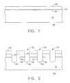
- a layer of photoresist 50is applied over silicon nitride layer 48 and is patterned as illustrated in cross section in FIG. 2 . Although not illustrated, the photoresist is left unpatterned and protecting the peripheral area of the IC.
- trenches 52are etched into the surface of silicon substrate 42 in the core area.
- the trenchesare anisotropically etched, for example by reactive ion etching (RIE) using a Cl or HBr/O 2 chemistry.
- RIEreactive ion etching
- the anisotropic etchingresults in trench walls 54 , 56 that are nearly vertical extending from surface 46 to the trench bottom 58 .
- the walls of trenches 52when viewed along their length, preferably are not straight, but rather are patterned and etched to leave enlarged contact regions 59 in the silicon substrate bordering the trenches. Most preferably, the contact regions are staggered from row to row to increase packing density. “Row” is used here in the context of rows and columns of a memory array. Word lines will eventually be formed along the row direction. The number and length of trenches will be determined by the size of the memory to be fabricated.
- thermal oxide 60is grown as an oxide liner on the walls and bottom of the trenches as illustrated in cross section in FIG. 3 .
- One or more layers of thermal oxidemay be grown and subsequently removed by etching before the growth of oxide 60 .
- the growth and stripping of the additional layers of thermal oxideremove etch damage caused by the trench etching.
- the peripheral areais protected by nitride layer 48 .
- Layer 60removes additional damage caused by the trench etching and prevents implant channeling during subsequent ion implantations.
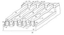
- FIG. 4illustrates, in a partially cut away perspective view, a portion of IC 40 at this stage of the processing.
- the areas indicated by diagonal shading lines 61are areas in which source and drain regions will be formed.
- the areas indicated by cross hatching 62are areas in which the channel regions of the memory transistors will be formed.
- double headed arrow 152indicates the length direction of trenches 52
- double headed arrow 154indicates the depth direction of the trenches.
- CMOS processing ionsare implanted into the surface of the substrate to form doped well regions in which the active transistors are formed.
- the well regionsare formed in the portions of the substrate forming the walls of trenches 52 .
- P-type ionsare implanted through thermal oxide 60 into the substrate forming the walls of the trenches to form P-doped wells 64 as illustrated in cross section in FIG. 5 .
- walls 54 , 56are nearly vertical, the ions are implanted at a high tilt angle determined by the depth of the trench and the proximity of the adjacent trench. Multiple implants may be used to tailor the concentration gradient of the dopant in the wells.
- An additional implantmay also be used to adjust the threshold voltage of the MOS transistors.
- the implantsare then activated by heating, for example by rapid thermal annealing (RTA).
- RTArapid thermal annealing
- the wellsare formed on both walls of the trenches so that vertical transistors can be formed in both walls, optimizing the density of transistors in a given unit of surface area.
- tunnel oxide 66has a thickness of about 8-9 nm.
- a layer of siliconeither amorphous or polycrystalline but hereinafter referred to as a poly layer, is deposited onto the layer of tunnel oxide.
- the poly layeris anisotropically etched, for example by RIE, to form poly spacers 68 extending from near the surface of the substrate but below the bottom of nitride layer 48 to the bottom of the trenches.
- the anisotropic etchingremoves the poly layer from the bottom of the trenches as well as from the nitride layer 48 and from the peripheral area.
- the tunnel oxidewould be the gate insulator of the MOS transistor and the poly spacer would form the gate electrode.
- the poly spacersare thermally oxidized to form a layer of oxide 70 having a thickness of about 4-5 nm and a layer of silicon nitride 72 having a thickness of about 8-9 nm is deposited over oxide layer 70 .
- a layer of photoresist(not illustrated) is applied and patterned to leave the patterned photoresist covering the silicon nitride that is located over the channel regions of the MOS transistors as indicated by cross hatching 62 in FIG. 4 .
- the patterned photoresistis used as an etch mask and the exposed silicon nitride and the poly layer underlying the exposed silicon nitride is etched, preferably in a high pressure isotropic plasma etch.
- the high pressure etchaids in removing silicon nitride from corners and otherwise difficult to etch areas.
- silicon nitride layer 72 and poly spacer 68are left covering only the channel regions.
- the nitride etchis controlled in length so that the bulk of silicon nitride layer 48 remains on the surface of the substrate.
- Patterned silicon nitride layer 72 and silicon nitride layer 48are together used as an oxidation mask and a thick thermal isolation oxide 74 is grown on the exposed silicon by heating in an oxidizing ambient.
- the exposed siliconis the silicon at the bottom 58 of trenches 52 as well as on the walls 54 , 56 of the trench in the areas indicated in FIG. 4 by diagonal shading lines 61 .
- the isolation oxideis grown as a LOCOS oxide.
- the thermal oxidation processalso grows a thin thermal oxide 76 on the surface of patterned silicon nitride layer 72 .
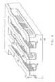
- FIG. 7illustrates, in a partially cut away perspective view, a portion of integrated circuit 40 at this stage of the processing.
- poly siliconAnother layer of silicon, either amorphous or polycrystalline but hereinafter referred to as poly silicon, is deposited to a thickness of about 200 nm.
- the poly silicon layeris doped N-type, and preferably is deposited as a doped layer. The doping can be phosphorus or arsenic, but preferably is phosphors.
- a layer of photoresist(not illustrated) is applied over the layer of poly silicon and is patterned as an etch mask for the layer of poly silicon.
- the poly silicon layeris etched using the patterned photoresist layer as an etch mask to form top contact or control gate 78 for memory transistors formed on wall 54 of trench 52 and top contact or control gate 80 for memory transistors formed on wall 56 of trench 52 .
- the patterned photoresist layeralso protects a contact area 82 coupled to control gate 78 and a contact area 84 coupled to control gate 80 , with both contact area 82 and 84 located on the surface of nitride layer 48 .
- the etching of the poly silicon layerwhich can be done as an anisotropic etch such as a RIE, leaves the poly silicon on the sidewall of trench 52 , but removes the poly silicon from all horizontal surfaces (except for contact areas 82 and 84 ) including the bottom of the trench and horizontal surfaces in both the core and peripheral areas.
- the patterned photoresist layeris removed and a further photoresist layer (again not illustrated) is applied and patterned.
- This further photoresist layeris patterned to protect all of the poly silicon except the poly silicon on the wall at the ends of the trenches. Using the patterned photoresist as an etch mask, the exposed poly silicon is etched to form a gap 86 at the end of each trench physically and electrically separating poly silicon control gate 78 from poly silicon control gate 80 .
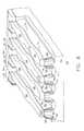
- FIG. 8illustrates, in a partially cut away perspective view, a portion of integrated circuit 40 at this stage of the processing.
- the poly silicon forming control gates 78 and 80extends along the length of trench 52 on the walls of the trench, and at the end of the trench extends up and onto the horizontal surface of nitride layer 48 to form contacts 82 and 84 .
- the three ONO layersare illustrated by a single layer 85 .
- a layer of oxide 90is deposited over the entire structure, in part to protect the core area from subsequent process steps to be performed in the peripheral area.
- the layer of oxideis photolithographically patterned to remove the oxide from the peripheral area while leaving the oxide covering and masking the core area. Using the patterned oxide as an etch mask, silicon nitride layer 48 is removed from the peripheral area. Until now, the silicon nitride layer has been masking the peripheral area from many of the process steps performed in the core area.
- N-wells and P-wellsare formed in the peripheral area in conventional manner to form the necessary substrate regions for the fabrication of CMOS peripheral transistors. Any remaining oxide is removed from the peripheral area, the surface of the peripheral area is cleaned, and a gate oxide layer is grown.
- the gate oxide layerpreferably having a thickness of 3-6 nm, will form the gate insulator of both the PMOS and the NMOS transistors of the peripheral circuitry.
- a layer of polycrystalline silicon having a thickness of about 150-200 nmis deposited overlying the layer of gate insulator.
- the layer of polycrystalline siliconis preferably deposited as an undoped polycrystalline layer and is subsequently doped with conductivity determining impurities during the formation of source and drain regions.
- the layer of polycrystalline siliconis patterned to form the gate electrodes of both the PMOS and the NMOS transistors of the peripheral circuitry.
- the portion of this polycrystalline silicon layer overlying the core areais etched and totally removed, either as part of the gate electrode forming etch step or in a separate etch step.
- the core areais protected by photoresist and source and drain extensions are ion implanted for first the PMOS transistors and then for the NMOS transistors of the periphery circuitry.
- a layer of silicon nitride 92is deposited to a thickness of about 90 nm.
- a layer of photoresist(not illustrated) is applied over the layer of silicon nitride and is photolithographically patterned to leave the photoresist covering all of the peripheral area and overlying the substrate between the trenches in the core area.
- layer of silicon nitride 92 and layer of oxide 90are etched to remove the nitride and oxide from the patterned poly silicon 78 and 80 and to leave the nitride and oxide overlying the substrate between the trenches as illustrated in FIG. 9 .
- the layer of patterned photoresistis removed and another layer of photoresist (not illustrated) is applied and patterned.
- the layer of patterned photoresistcovers the peripheral area and all of the core area except for a portion of each of contact regions 59 .
- the patterned photoresistis used as an etch mask and layer of nitride 92 , layer of oxide 90 and layer of nitride 48 exposed in the contact regions are etched to form an opening 93 as illustrated in cross section in FIG. 10 to allow a subsequent ion implantation into the contact regions.
- FIG. 10illustrates a cross section through only one of contact regions 59 . Recall that the contact areas are also the regions along the length of the trench in which isolating oxide 74 was grown.
- nitride layer 92is anisotropically etched to form spacers on the sidewalls of the gate electrodes in the peripheral area.
- the PMOS transistorsare masked with photoresist and N-type ions are implanted to form the source and drain regions of the NMOS transistors in the peripheral area.
- the N-type ionsare also implanted into the exposed portions of contact regions 59 in the core area to form drain regions 94 and source regions 95 alternating in the substrate along the length of trench 52 as illustrated in top view in FIG.
- Channels 97 of the MOS transistorsexist along the walls of the trench between the source and drain regions. In operation, current flows through the channel between the source and drain regions in a direction along the length of the trench. Isolation oxide 74 separates each channel from adjacent channels.
- the NMOS transistors and the core areaare then masked with photoresist and P-type ions are implanted to form the source and drain regions of the PMOS transistors in the peripheral area. Following the implantations, the patterned photoresist is patterned and the implants are annealed, for example by RTA. Drain regions 94 and source regions 95 , formed in the substrate bounding trenches 52 , extend from the surface of the substrate to the bottom of the trench as illustrated in FIG. 12 which shows an exemplary drain region in cross section.
- Any residual oxideis removed from the implanted regions including the gate electrodes and also from the poly silicon forming control gates 78 and 80 and contact area 82 and 84 , for example by etching in dilute hydrofluoric acid.
- a silicide forming metalsuch as cobalt is blanket deposited and heated, for example by RTA, to form a metal silicide (not illustrated) in those locations where the metal is in contact with silicon.
- the metal silicideforms on the source regions, drain regions, and gate electrodes of the peripheral transistors and on the contact regions 59 forming contacts to source and drain regions 94 and 95 , control gates 78 and 80 and contact areas 82 and 84 in the core area.
- the silicide forming metal that is not in contact with exposed silicondoes not react during the RTA and can be removed, for example by washing in a H 2 O 2 /H 2 SO 4 or HNO 3 /HCl solution. After silicidation a layer of oxide is blanket deposited to a thickness great enough to fill trenches 52 . The excess oxide can be removed and the upper surface of the oxide layer is planarized, for example by CMP. Contact openings are etched through the planarized oxide to expose the surface of drain regions 94 , source regions 95 , and contact areas 82 and 84 . Contact openings are also formed in the peripheral area to allow electrical contact to source and drain regions and to gate electrodes as necessary for the circuit function being implemented.
- bit lines 102electrically contact drain regions 94
- source lineselectrically contact source lines 95
- word line contacts 106electrically contact control gates 78 and 80 .
- the metal linescan be aluminum, copper, alloys of those metals, or other conductive materials commonly used for interconnection on a semiconductor integrated circuit.
- plug structuremay be used to directly contact the metal silicide and fill the contact openings.
- the plug structuremay include, for example, sequential layers of titanium, titanium nitride, and tungsten as is well known.
- bit lines, source lines, and word linesare all illustrated to be on a single level, it may be advantageous, for optimum layout reasons, to form the bit lines and source lines in one layer of metal and to form the word lines in another layer of metal separated from the bit lines by a layer of inter level dielectric.
- Integrated circuit 40can be completed with the conventional back end of line processing which, being conventional, will not be described herein.
Landscapes
- Engineering & Computer Science (AREA)
- Manufacturing & Machinery (AREA)
- Physics & Mathematics (AREA)
- Condensed Matter Physics & Semiconductors (AREA)
- General Physics & Mathematics (AREA)
- Computer Hardware Design (AREA)
- Microelectronics & Electronic Packaging (AREA)
- Power Engineering (AREA)
- Semiconductor Memories (AREA)
- Non-Volatile Memory (AREA)
- Element Separation (AREA)
Abstract
Description
- The present invention generally relates to a vertical semiconductor device, and more particularly relates to a vertical MOS device fabricated in the wall of a trench formed in a semiconductor substrate and having a channel along the edge of the trench parallel to the surface of the semiconductor substrate.
- The majority of present day integrated circuits (ICs) are implemented by using a plurality of interconnected field effect transistors (FETs), also called metal oxide semiconductor field effect transistors (MOSFETs), or simply MOS transistors. An MOS transistor includes a gate electrode as a control electrode and spaced apart source and drain regions between which a current can flow. A control voltage applied to the gate electrode controls the flow of current through a channel between the source and drain electrodes.
- ICs are typically fabricated in and on a thin semiconductor substrate having a substantially planar surface. The source and drain regions are spaced apart impurity doped regions ion implanted into the substantially planar surface on opposite sides of the gate electrode which is formed overlying the planar surface. As the complexity of the integrated circuits increases, more and more MOS transistors are needed to implement the integrated circuit function. As more and more transistors are designed into the IC, it becomes important to shrink the size of individual MOS transistors so that the size of the IC remains reasonable and the IC can be reliably manufactured. Shrinking the size of an MOS transistor implies that the minimum feature size, that is, the minimum width of a line or the minimum spacing between lines, is reduced. MOS transistors have now been aggressively reduced to the point at which the gate electrode of the transistor is less than or equal to 90 nanometers (nm) in width. Aggressively shrinking the minimum feature size even further to incorporate more devices in and on the planar substrate surface, however, will incur a significant increase in manufacturing cost, in terms of increased capital expenditures and reduced yield.
- Attempts have been made to overcome the problem of packing more and more transistors onto the semiconductor surface by manufacturing vertical transistors. In such attempts, instead of locating each of the source, drain, and channel on the substantially planar surface of the substrate, the vertical transistors are fabricated in trenches that are etched into the surface of the substrate with a source at the bottom of the trench, a drain at the top of the trench near the semiconductor surface, and a channel conducting current along the wall of the trench between the source and the drain. Unfortunately, such attempts have been largely unsuccessful because of problems of isolating one transistor from another and of making the necessary electrical contacts to the vertical transistor elements.
- Accordingly, it is desirable to provide a vertical device structure that allow an increase in the number of devices integrated in an IC without requiring a further reduction in minimum feature size. In addition, it is desirable to provide a memory IC based on a vertical transistor structure. Furthermore, other desirable features and characteristics of the present invention will become apparent from the subsequent detailed description and the appended claims, taken in conjunction with the accompanying drawings and the foregoing technical field and background.
- A vertical semiconductor device and a method for its fabrication are provided. The semiconductor device comprises a trench formed in the semiconductor substrate and bounded by a trench wall extending from the semiconductor surface to a trench bottom. A drain region and a source region, spaced apart along the length of the trench, are formed along the trench wall, each extending from the surface toward the bottom. A channel region is formed in the substrate along the trench wall between the drain region and the source region and extending along the length of the trench parallel to the substrate surface. A gate insulator and a gate electrode are formed overlying the channel.
- The present invention will hereinafter be described in conjunction with the following drawing figures, wherein like numerals denote like elements, and wherein
FIG. 1-13 illustrate a portion of a semiconductor device and method steps for its fabrication in accordance with various embodiments of the invention. - The following detailed description is merely exemplary in nature and is not intended to limit the invention or the application and uses of the invention. Furthermore, there is no intention to be bound by any expressed or implied theory presented in the preceding technical field, background, brief summary or the following detailed description. Terms such as “vertical” and “horizontal” are used herein for descriptive purposes and refer only to orientation with respect to the surface of a substrate (taken to be horizontal), and are not intended to otherwise limit the orientation of the inventive device.
FIGS. 1-13 schematically illustrate a semiconductor memory integratedcircuit 40 and method steps for the fabrication of integratedcircuit 40 in accordance with various embodiments of the invention. Although the term “MOS device” properly refers to a device having a metal gate electrode and an oxide gate insulator, that term will be used throughout to refer to any semiconductor device that includes a conductive gate electrode (whether metal or other conductive material) that is positioned over a gate insulator (whether oxide or other insulator) which, in turn, is positioned over a semiconductor substrate. In these illustrative embodiments only a small portion of integratedcircuit 40 is illustrated. Various steps in the manufacture of MOS devices are well known and so, in the interest of brevity, many conventional steps will only be mentioned briefly herein or will be omitted entirely without providing the well known process details. In this exemplary embodiment integratedcircuit 40 is illustrated to be a non-volatile memory circuit such as an electrically erasable programmable read only memory (EEPROM) or a Flash memory, but the invention is also applicable to other semiconductor memory circuits as well as to other ICs, especially those that have a repetitive structure.- A semiconductor memory IC typically includes a memory array or core area and a peripheral area. The core area, in which data is stored, usually, but not necessarily, includes only N-channel MOS (NMOS) transistors and the exemplary embodiment described below will be such an NMOS circuit. The invention is not limited, however, to such single channel embodiments. The peripheral area, which includes support circuitry such as clock circuits, address circuits, I/O circuits, and the like, usually includes complementary MOS (CMOS) transistors. In accordance with an embodiment of the invention, the peripheral circuitry is conventional and is fabricated in substantially the conventional manner with conventional (not vertical) CMOS transistors. Because the peripheral circuitry is fabricated in conventional manner, the peripheral circuitry and the process steps for fabricating such circuitry will not be illustrated or described except to discuss how such conventional process steps are integrated process for fabricating the core area. Accordingly, the drawing figures will illustrate only (a portion of) the core area of integrated
circuit 40. - As illustrated in
FIG. 1 , fabrication of a semiconductor device in accordance with one embodiment of the invention begins with providing asemiconductor substrate 42. Although other semiconductor materials can be used, the semiconductor substrate is preferably a silicon substrate, either a bulk substrate or a silicon on insulator (SOI) substrate. Without limitation, the semiconductor substrate will generally be referred to herein as a silicon substrate. As used herein, the term “silicon substrate” will be used to encompass the relatively pure monocrystalline silicon materials typically used in the semiconductor industry, either bulk or SOI, as well as silicon admixed with other elements such as germanium, carbon, and the like to form substantially monocrystalline semiconductor material. - In accordance with a preferred embodiment of the invention isolation in the peripheral portion of the IC, preferably shallow trench isolation (STI), is formed first. Because the peripheral isolation is formed in conventional manner, the process steps for its formation will not be described in detail and will not be illustrated in the drawing figures. Although many techniques can be used for forming STI, all such methods generally involve forming a pad oxide and a layer of nitride on the silicon substrate, patterning the nitride and oxide as an etch mask, etching trenches into the surface of the substrate, filling the trenches with an oxide or other insulator, and removing the excess oxide, for example by chemical mechanical planarization (CMP). During the formation of the peripheral isolation the core area is protected by the silicon nitride layer that is left unpatterned over the core area.
- As illustrated in cross section in
FIG. 1 , in accordance with an embodiment of the invention, a thin layer ofoxide 44 is formed onsurface 46 of the silicon substrate. A layer ofsilicon nitride 48, having a thickness of about 90 nm is deposited over the layer of oxide. Layer ofoxide 44 can be grown by heating the silicon substrate in an oxidizing ambient and layer ofsilicon nitride 48 can be deposited by low pressure chemical vapor deposition (LPCVD) by the reaction of dichlorosilane and ammonia. - A layer of
photoresist 50 is applied oversilicon nitride layer 48 and is patterned as illustrated in cross section inFIG. 2 . Although not illustrated, the photoresist is left unpatterned and protecting the peripheral area of the IC. Using the patterned photoresist as an etch mask,trenches 52 are etched into the surface ofsilicon substrate 42 in the core area. Preferably the trenches are anisotropically etched, for example by reactive ion etching (RIE) using a Cl or HBr/O2chemistry. The anisotropic etching results intrench walls surface 46 to thetrench bottom 58. Although not apparent inFIG. 2 (but illustrated inFIG. 4 below) the walls oftrenches 52, when viewed along their length, preferably are not straight, but rather are patterned and etched to leave enlargedcontact regions 59 in the silicon substrate bordering the trenches. Most preferably, the contact regions are staggered from row to row to increase packing density. “Row” is used here in the context of rows and columns of a memory array. Word lines will eventually be formed along the row direction. The number and length of trenches will be determined by the size of the memory to be fabricated. - After completing the trench etch,
photoresist layer 50 is stripped and a thin layer ofthermal oxide 60 is grown as an oxide liner on the walls and bottom of the trenches as illustrated in cross section inFIG. 3 . One or more layers of thermal oxide (not illustrated) may be grown and subsequently removed by etching before the growth ofoxide 60. The growth and stripping of the additional layers of thermal oxide remove etch damage caused by the trench etching. During the growth and stripping the peripheral area is protected bynitride layer 48.Layer 60 removes additional damage caused by the trench etching and prevents implant channeling during subsequent ion implantations.FIG. 4 illustrates, in a partially cut away perspective view, a portion ofIC 40 at this stage of the processing. The areas indicated bydiagonal shading lines 61 are areas in which source and drain regions will be formed. The areas indicated by cross hatching62 are areas in which the channel regions of the memory transistors will be formed. Just for clarity of understanding, double headedarrow 152 indicates the length direction oftrenches 52, and double headedarrow 154 indicates the depth direction of the trenches. - In conventional CMOS processing ions are implanted into the surface of the substrate to form doped well regions in which the active transistors are formed. In accordance with an embodiment of this invention the well regions are formed in the portions of the substrate forming the walls of
trenches 52. Because the core of the IC will be formed of NMOS transistors, P-type ions are implanted throughthermal oxide 60 into the substrate forming the walls of the trenches to form P-dopedwells 64 as illustrated in cross section inFIG. 5 . Becausewalls - In accordance with this exemplary embodiment of the invention, specifically if the semiconductor device being fabricated is a non-volatile memory IC, thin
thermal oxide 60 is stripped and athin tunnel oxide 66 is grown on the walls and bottom oftrenches 52 as illustrated in cross section inFIG. 6 . Preferablytunnel oxide 66 has a thickness of about 8-9 nm. A layer of silicon, either amorphous or polycrystalline but hereinafter referred to as a poly layer, is deposited onto the layer of tunnel oxide. The poly layer is anisotropically etched, for example by RIE, to formpoly spacers 68 extending from near the surface of the substrate but below the bottom ofnitride layer 48 to the bottom of the trenches. The anisotropic etching removes the poly layer from the bottom of the trenches as well as from thenitride layer 48 and from the peripheral area. In forming a volatile device, the tunnel oxide would be the gate insulator of the MOS transistor and the poly spacer would form the gate electrode. Continuing the process for fabricating a non-volatile memory device, the poly spacers are thermally oxidized to form a layer ofoxide 70 having a thickness of about 4-5 nm and a layer ofsilicon nitride 72 having a thickness of about 8-9 nm is deposited overoxide layer 70. - A layer of photoresist (not illustrated) is applied and patterned to leave the patterned photoresist covering the silicon nitride that is located over the channel regions of the MOS transistors as indicated by cross hatching62 in
FIG. 4 . The patterned photoresist is used as an etch mask and the exposed silicon nitride and the poly layer underlying the exposed silicon nitride is etched, preferably in a high pressure isotropic plasma etch. The high pressure etch aids in removing silicon nitride from corners and otherwise difficult to etch areas. After the etch,silicon nitride layer 72 andpoly spacer 68 are left covering only the channel regions. The nitride etch is controlled in length so that the bulk ofsilicon nitride layer 48 remains on the surface of the substrate. Patternedsilicon nitride layer 72 andsilicon nitride layer 48 are together used as an oxidation mask and a thickthermal isolation oxide 74 is grown on the exposed silicon by heating in an oxidizing ambient. The exposed silicon is the silicon at the bottom58 oftrenches 52 as well as on thewalls FIG. 4 by diagonal shading lines61. The isolation oxide is grown as a LOCOS oxide. The thermal oxidation process also grows a thinthermal oxide 76 on the surface of patternedsilicon nitride layer 72.Thermal oxide 76, together with patternedsilicon nitride layer 72 andoxide layer 70 form an oxide-nitride-oxide (ONO) memory film or memory stack onpoly layer 68.FIG. 7 illustrates, in a partially cut away perspective view, a portion ofintegrated circuit 40 at this stage of the processing. - Another layer of silicon, either amorphous or polycrystalline but hereinafter referred to as poly silicon, is deposited to a thickness of about 200 nm. The poly silicon layer is doped N-type, and preferably is deposited as a doped layer. The doping can be phosphorus or arsenic, but preferably is phosphors. A layer of photoresist (not illustrated) is applied over the layer of poly silicon and is patterned as an etch mask for the layer of poly silicon. The poly silicon layer is etched using the patterned photoresist layer as an etch mask to form top contact or control
gate 78 for memory transistors formed onwall 54 oftrench 52 and top contact or controlgate 80 for memory transistors formed onwall 56 oftrench 52. The patterned photoresist layer also protects acontact area 82 coupled to controlgate 78 and acontact area 84 coupled to controlgate 80, with bothcontact area nitride layer 48. The etching of the poly silicon layer, which can be done as an anisotropic etch such as a RIE, leaves the poly silicon on the sidewall oftrench 52, but removes the poly silicon from all horizontal surfaces (except forcontact areas 82 and84) including the bottom of the trench and horizontal surfaces in both the core and peripheral areas. The patterned photoresist layer is removed and a further photoresist layer (again not illustrated) is applied and patterned. This further photoresist layer is patterned to protect all of the poly silicon except the poly silicon on the wall at the ends of the trenches. Using the patterned photoresist as an etch mask, the exposed poly silicon is etched to form agap 86 at the end of each trench physically and electrically separating polysilicon control gate 78 from polysilicon control gate 80.FIG. 8 illustrates, in a partially cut away perspective view, a portion ofintegrated circuit 40 at this stage of the processing. The poly silicon formingcontrol gates trench 52 on the walls of the trench, and at the end of the trench extends up and onto the horizontal surface ofnitride layer 48 to formcontacts single layer 85. - Having completed a much of the core area of
IC 40, the process now continues by processing a portion of the peripheral area. Again, as these process steps are conventional, they need not be described or illustrated in detail. A layer ofoxide 90 is deposited over the entire structure, in part to protect the core area from subsequent process steps to be performed in the peripheral area. The layer of oxide is photolithographically patterned to remove the oxide from the peripheral area while leaving the oxide covering and masking the core area. Using the patterned oxide as an etch mask,silicon nitride layer 48 is removed from the peripheral area. Until now, the silicon nitride layer has been masking the peripheral area from many of the process steps performed in the core area. After removing the silicon nitride layer, N-wells and P-wells are formed in the peripheral area in conventional manner to form the necessary substrate regions for the fabrication of CMOS peripheral transistors. Any remaining oxide is removed from the peripheral area, the surface of the peripheral area is cleaned, and a gate oxide layer is grown. The gate oxide layer, preferably having a thickness of 3-6 nm, will form the gate insulator of both the PMOS and the NMOS transistors of the peripheral circuitry. A layer of polycrystalline silicon having a thickness of about 150-200 nm is deposited overlying the layer of gate insulator. The layer of polycrystalline silicon is preferably deposited as an undoped polycrystalline layer and is subsequently doped with conductivity determining impurities during the formation of source and drain regions. The layer of polycrystalline silicon is patterned to form the gate electrodes of both the PMOS and the NMOS transistors of the peripheral circuitry. The portion of this polycrystalline silicon layer overlying the core area is etched and totally removed, either as part of the gate electrode forming etch step or in a separate etch step. The core area is protected by photoresist and source and drain extensions are ion implanted for first the PMOS transistors and then for the NMOS transistors of the periphery circuitry. - A layer of
silicon nitride 92 is deposited to a thickness of about 90 nm. A layer of photoresist (not illustrated) is applied over the layer of silicon nitride and is photolithographically patterned to leave the photoresist covering all of the peripheral area and overlying the substrate between the trenches in the core area. Using the patterned photoresist as an etch mask, layer ofsilicon nitride 92 and layer ofoxide 90 are etched to remove the nitride and oxide from the patternedpoly silicon FIG. 9 . - The layer of patterned photoresist is removed and another layer of photoresist (not illustrated) is applied and patterned. The layer of patterned photoresist covers the peripheral area and all of the core area except for a portion of each of
contact regions 59. The patterned photoresist is used as an etch mask and layer ofnitride 92, layer ofoxide 90 and layer ofnitride 48 exposed in the contact regions are etched to form anopening 93 as illustrated in cross section inFIG. 10 to allow a subsequent ion implantation into the contact regions.FIG. 10 illustrates a cross section through only one ofcontact regions 59. Recall that the contact areas are also the regions along the length of the trench in which isolatingoxide 74 was grown. - The layer of patterned photoresist is removed and another layer of photoresist (not illustrated) is applied and patterned to leave the photoresist covering and protecting all of the core area. With the core area protected,
nitride layer 92 is anisotropically etched to form spacers on the sidewalls of the gate electrodes in the peripheral area. After forming the spacers, the PMOS transistors are masked with photoresist and N-type ions are implanted to form the source and drain regions of the NMOS transistors in the peripheral area. The N-type ions are also implanted into the exposed portions ofcontact regions 59 in the core area to formdrain regions 94 andsource regions 95 alternating in the substrate along the length oftrench 52 as illustrated in top view inFIG. 11 .Channels 97 of the MOS transistors exist along the walls of the trench between the source and drain regions. In operation, current flows through the channel between the source and drain regions in a direction along the length of the trench.Isolation oxide 74 separates each channel from adjacent channels. The NMOS transistors and the core area are then masked with photoresist and P-type ions are implanted to form the source and drain regions of the PMOS transistors in the peripheral area. Following the implantations, the patterned photoresist is patterned and the implants are annealed, for example by RTA.Drain regions 94 andsource regions 95, formed in thesubstrate bounding trenches 52, extend from the surface of the substrate to the bottom of the trench as illustrated inFIG. 12 which shows an exemplary drain region in cross section. - Any residual oxide is removed from the implanted regions including the gate electrodes and also from the poly silicon forming
control gates contact area contact regions 59 forming contacts to source and drainregions control gates contact areas trenches 52. The excess oxide can be removed and the upper surface of the oxide layer is planarized, for example by CMP. Contact openings are etched through the planarized oxide to expose the surface ofdrain regions 94,source regions 95, andcontact areas - As illustrated in top view in
FIG. 13 , a layer of metal is deposited on the surface of the planarized oxide layer and is patterned to formbit lines 102, source lines104, andword line contacts 106.Bit lines 102 electricallycontact drain regions 94, source lines electrically contact source lines95, andword line contacts 106 electricallycontact control gates - Integrated
circuit 40 can be completed with the conventional back end of line processing which, being conventional, will not be described herein. - While at least one exemplary embodiment has been presented in the foregoing detailed description, it should be appreciated that a vast number of variations exist. It should also be appreciated that the exemplary embodiment or exemplary embodiments are only examples, and are not intended to limit the scope, applicability, or configuration of the invention in any way. Rather, the foregoing detailed description will provide those skilled in the art with a convenient road map for implementing the exemplary embodiment or exemplary embodiments. It should be understood that various changes can be made in the function and arrangement of elements without departing from the scope of the invention as set forth in the appended claims and the legal equivalents thereof.
Claims (20)
Priority Applications (6)
| Application Number | Priority Date | Filing Date | Title |
|---|---|---|---|
| US11/378,463US7859026B2 (en) | 2006-03-16 | 2006-03-16 | Vertical semiconductor device |
| CN2007800092020ACN101401196B (en) | 2006-03-16 | 2007-03-16 | Vertical EEPROM device |
| KR1020087022644AKR101078013B1 (en) | 2006-03-16 | 2007-03-16 | Vertical eeprom device |
| PCT/US2007/006715WO2007109179A1 (en) | 2006-03-16 | 2007-03-16 | Vertical eeprom device |
| EP07753350AEP1994557A1 (en) | 2006-03-16 | 2007-03-16 | Vertical eeprom device |
| TW096109048ATWI368992B (en) | 2006-03-16 | 2007-03-16 | Vertical semiconductor device |
Applications Claiming Priority (1)
| Application Number | Priority Date | Filing Date | Title |
|---|---|---|---|
| US11/378,463US7859026B2 (en) | 2006-03-16 | 2006-03-16 | Vertical semiconductor device |
Publications (2)
| Publication Number | Publication Date |
|---|---|
| US20070215940A1true US20070215940A1 (en) | 2007-09-20 |
| US7859026B2 US7859026B2 (en) | 2010-12-28 |
Family
ID=38349446
Family Applications (1)
| Application Number | Title | Priority Date | Filing Date |
|---|---|---|---|
| US11/378,463Active2027-03-31US7859026B2 (en) | 2006-03-16 | 2006-03-16 | Vertical semiconductor device |
Country Status (6)
| Country | Link |
|---|---|
| US (1) | US7859026B2 (en) |
| EP (1) | EP1994557A1 (en) |
| KR (1) | KR101078013B1 (en) |
| CN (1) | CN101401196B (en) |
| TW (1) | TWI368992B (en) |
| WO (1) | WO2007109179A1 (en) |
Cited By (12)
| Publication number | Priority date | Publication date | Assignee | Title |
|---|---|---|---|---|
| US20080296664A1 (en)* | 2007-05-25 | 2008-12-04 | Krishnaswamy Ramkumar | Integration of non-volatile charge trap memory devices and logic cmos devices |
| US20130178031A1 (en)* | 2007-05-25 | 2013-07-11 | Cypress Semiconductor Corporation | Integration of non-volatile charge trap memory devices and logic cmos devices |
| US8859374B1 (en) | 2007-05-25 | 2014-10-14 | Cypress Semiconductor Corporation | Memory transistor with multiple charge storing layers and a high work function gate electrode |
| US20150187960A1 (en) | 2007-05-25 | 2015-07-02 | Cypress Semiconductor Corporation | Radical Oxidation Process For Fabricating A Nonvolatile Charge Trap Memory Device |
| US9299568B2 (en) | 2007-05-25 | 2016-03-29 | Cypress Semiconductor Corporation | SONOS ONO stack scaling |
| US9349877B1 (en) | 2007-05-25 | 2016-05-24 | Cypress Semiconductor Corporation | Nitridation oxidation of tunneling layer for improved SONOS speed and retention |
| US9355849B1 (en) | 2007-05-25 | 2016-05-31 | Cypress Semiconductor Corporation | Oxide-nitride-oxide stack having multiple oxynitride layers |
| US9929240B2 (en) | 2007-05-25 | 2018-03-27 | Cypress Semiconductor Corporation | Memory transistor with multiple charge storing layers and a high work function gate electrode |
| US10374067B2 (en) | 2007-05-25 | 2019-08-06 | Longitude Flash Memory Solutions Ltd. | Oxide-nitride-oxide stack having multiple oxynitride layers |
| US10615289B2 (en) | 2007-12-12 | 2020-04-07 | Longitude Flash Memory Solutions Ltd. | Nonvolatile charge trap memory device having a high dielectric constant blocking region |
| US20220131005A1 (en)* | 2020-10-23 | 2022-04-28 | Stmicroelectronics (Crolles 2) Sas | Semiconductor integrated circuit component |
| US20220293519A1 (en)* | 2021-03-10 | 2022-09-15 | Nanya Technology Corporation | Semiconductor device structure with serpentine conductive feature and method for forming the same |
Families Citing this family (3)
| Publication number | Priority date | Publication date | Assignee | Title |
|---|---|---|---|---|
| US8993993B2 (en)* | 2010-05-11 | 2015-03-31 | Samsung Electronics Co., Ltd. | Semiconductor light emitting device and method for fabricating the same |
| US8878156B2 (en) | 2011-11-21 | 2014-11-04 | Avalanche Technology Inc. | Memory device having stitched arrays of 4 F2 memory cells |
| US12336264B2 (en)* | 2022-06-21 | 2025-06-17 | Nanya Technology Corporation | Semiconductor device having gate electrodes with dopant of different conductive types |
Citations (93)
| Publication number | Priority date | Publication date | Assignee | Title |
|---|---|---|---|---|
| US4728619A (en)* | 1987-06-19 | 1988-03-01 | Motorola, Inc. | Field implant process for CMOS using germanium |
| US4878102A (en)* | 1986-03-27 | 1989-10-31 | U.S. Philips Corp. | Charge-coupled device |
| US4931409A (en)* | 1988-01-30 | 1990-06-05 | Kabushiki Kaisha Toshiba | Method of manufacturing semiconductor device having trench isolation |
| US5021359A (en)* | 1988-06-21 | 1991-06-04 | Harris Corporation | Radiation hardened complementary transistor integrated circuits |
| US5045489A (en)* | 1989-06-30 | 1991-09-03 | Texas Instruments Incorporated | Method of making a high-speed 2-transistor cell for programmable/EEPROM devices with separate read and write transistors |
| US5135879A (en)* | 1985-03-26 | 1992-08-04 | Texas Instruments Incorporated | Method of fabricating a high density EPROM cell on a trench wall |
| US5177576A (en)* | 1990-05-09 | 1993-01-05 | Hitachi, Ltd. | Dynamic random access memory having trench capacitors and vertical transistors |
| US5210046A (en)* | 1989-12-22 | 1993-05-11 | Scs-Thomas Microelectronics S.R.L. | Method of fabricating eprom device with metallic source connections |
| US5293061A (en)* | 1990-04-09 | 1994-03-08 | Seiko Instruments Inc. | Semiconductor device having an isolation layer region on the side wall of a groove |
| US5298775A (en)* | 1990-02-26 | 1994-03-29 | Nec Corporation | Semiconductor memory device having stacked-type capacitor of large capacitance |
| US5327374A (en)* | 1990-07-03 | 1994-07-05 | Siemens Aktiengesellschaft | Arrangement with self-amplifying dynamic MOS transistor storage cells |
| US5338953A (en)* | 1991-06-20 | 1994-08-16 | Mitsubishi Denki Kabushiki Kaisha | Electrically erasable and programmable semiconductor memory device with trench memory transistor and manufacturing method of the same |
| US5411905A (en)* | 1994-04-29 | 1995-05-02 | International Business Machines Corporation | Method of making trench EEPROM structure on SOI with dual channels |
| US5432739A (en)* | 1994-06-17 | 1995-07-11 | Philips Electronics North America Corporation | Non-volatile sidewall memory cell method of fabricating same |
| US5491356A (en)* | 1990-11-19 | 1996-02-13 | Micron Technology, Inc. | Capacitor structures for dynamic random access memory cells |
| US5508544A (en)* | 1992-12-14 | 1996-04-16 | Texas Instruments Incorporated | Three dimensional FAMOS memory devices |
| US5559357A (en)* | 1992-09-21 | 1996-09-24 | Krivokapic; Zoran | Poly LDD self-aligned channel transistors |
| US5627097A (en)* | 1995-07-03 | 1997-05-06 | Motorola, Inc. | Method for making CMOS device having reduced parasitic capacitance |
| US5629226A (en)* | 1992-07-13 | 1997-05-13 | Kabushiki Kaisha Toshiba | Method of manufacturing a buried plate type DRAM having a widened trench structure |
| US5637896A (en)* | 1994-07-15 | 1997-06-10 | United Microelectronics Corporation | High coupling ratio flash memory cell |
| US5705415A (en)* | 1994-10-04 | 1998-01-06 | Motorola, Inc. | Process for forming an electrically programmable read-only memory cell |
| US5705409A (en)* | 1995-09-28 | 1998-01-06 | Motorola Inc. | Method for forming trench transistor structure |
| US5741716A (en)* | 1995-11-03 | 1998-04-21 | Hyundai Electronics Industries Co., Ltd. | Method for fabricating thin film transistor |
| US5789306A (en)* | 1996-04-18 | 1998-08-04 | Micron Technology, Inc. | Dual-masked field isolation |
| US5804854A (en)* | 1996-08-30 | 1998-09-08 | Hyundai Electronics Industries Co., Ltd. | Memory cell array |
| US5861330A (en)* | 1997-05-07 | 1999-01-19 | International Business Machines Corporation | Method and structure to reduce latch-up using edge implants |
| US5872037A (en)* | 1995-06-20 | 1999-02-16 | Mitsubishi Denki Kabushiki Kaisha | Method for manufacturing a vertical mosfet including a back gate electrode |
| US6015725A (en)* | 1996-08-22 | 2000-01-18 | Sony Corporation | Vertical field effect transistor and manufacturing method thereof |
| US6040210A (en)* | 1997-01-22 | 2000-03-21 | International Business Machines Corporation | 2F-square memory cell for gigabit memory applications |
| US6077745A (en)* | 1997-01-22 | 2000-06-20 | International Business Machines Corporation | Self-aligned diffused source vertical transistors with stack capacitors in a 4F-square memory cell array |
| US6097621A (en)* | 1998-05-04 | 2000-08-01 | Texas Instruments Incorporated | Memory cell array architecture for random access memory device |
| US6097065A (en)* | 1998-03-30 | 2000-08-01 | Micron Technology, Inc. | Circuits and methods for dual-gated transistors |
| US6124608A (en)* | 1997-12-18 | 2000-09-26 | Advanced Micro Devices, Inc. | Non-volatile trench semiconductor device having a shallow drain region |
| US6133098A (en)* | 1999-05-17 | 2000-10-17 | Halo Lsi Design & Device Technology, Inc. | Process for making and programming and operating a dual-bit multi-level ballistic flash memory |
| US6137134A (en)* | 1997-05-28 | 2000-10-24 | Nec Corporation | Semiconductor memory device |
| US6141236A (en)* | 1999-03-10 | 2000-10-31 | Alliance Semiconductor Corporation | Interleaved stitch using segmented word lines |
| US6211014B1 (en)* | 1997-04-15 | 2001-04-03 | United Microelectronics Corp. | Three-dimensional, deep-trench, high-density read-only memory (ROM) and its manufacturing method |
| US6243293B1 (en)* | 1992-01-29 | 2001-06-05 | Interuniversitair Micro-Elektronica Centrum | Contacted cell array configuration for erasable and programmable semiconductor memories |
| US6246083B1 (en)* | 1998-02-24 | 2001-06-12 | Micron Technology, Inc. | Vertical gain cell and array for a dynamic random access memory |
| US6248645B1 (en)* | 1998-05-28 | 2001-06-19 | Kabushiki Kaisha Toshiba | Semiconductor device having buried-type element isolation structure and method of manufacturing the same |
| US6303439B1 (en)* | 1999-11-24 | 2001-10-16 | United Microelectronics Corp. | Fabrication method for a two-bit flash memory cell |
| US6335237B1 (en)* | 2000-03-03 | 2002-01-01 | Micron Technology, Inc. | Methods of forming capacitor and bitline structures |
| US20020031887A1 (en)* | 1996-05-06 | 2002-03-14 | Harshfield Steven T. | ZPROM manufacture and design and methods for forming thin structures using spacers as an etching mask |
| US20020048875A1 (en)* | 1995-07-24 | 2002-04-25 | Monte Manning | Thin film transistors and methods of forming thin film transistors |
| US6391726B1 (en)* | 1999-03-11 | 2002-05-21 | Micron Technology, Inc. | Method of fabricating integrated circuitry |
| US6437397B1 (en)* | 1997-12-05 | 2002-08-20 | Taiwan Semiconductor Manufacturing Company | Flash memory cell with vertically oriented channel |
| US20020121673A1 (en)* | 2000-08-31 | 2002-09-05 | Keiji Jono | Methods of forming an isolation trench in a semiconductor, methods of forming an isolation trench in a surface of a silicon wafer, methods of forming an isolation trench-isolated transistor, trench-isolated transistor, trench isolation structures formed in a semiconductor, memory cells and DRAMs |
| US20020158273A1 (en)* | 2000-10-17 | 2002-10-31 | Hitachi, Ltd. | Nonvolatile semiconductor memory device and a method of manufacturing the same |
| US6504200B2 (en)* | 1999-03-12 | 2003-01-07 | Infineon Technologies Ag | DRAM cell configuration and fabrication method |
| US6518628B1 (en)* | 1997-05-15 | 2003-02-11 | Siemens Aktiengesellschaft | Integrated CMOS circuit configuration, and production of same |
| US6559491B2 (en)* | 2001-02-09 | 2003-05-06 | Micron Technology, Inc. | Folded bit line DRAM with ultra thin body transistors |
| US6566202B2 (en)* | 1997-05-14 | 2003-05-20 | Siemens Aktiengesellschaft | Integrated circuit having at least two vertical MOS transistors and method for manufacturing same |
| US6566187B1 (en)* | 1998-09-30 | 2003-05-20 | Infineon Technologies Ag | DRAM cell system and method for producing same |
| US6610575B1 (en)* | 2002-06-04 | 2003-08-26 | Chartered Semiconductor Manufacturing Ltd. | Forming dual gate oxide thickness on vertical transistors by ion implantation |
| US6680501B2 (en)* | 2001-03-23 | 2004-01-20 | Hitachi, Ltd. | Semiconductor device |
| US20040026737A1 (en)* | 2002-05-28 | 2004-02-12 | Markus Zundel | MOS transistor device |
| US6700150B1 (en)* | 2002-08-20 | 2004-03-02 | Intelligent Sources Development Corp. | Self-aligned vertical transistor DRAM structure |
| US6730961B2 (en)* | 2001-12-18 | 2004-05-04 | Fuji Electric Co., Ltd. | Semiconductor device |
| US6734058B2 (en)* | 2001-12-29 | 2004-05-11 | Dongbu Electronics Co., Ltd. | Method for fabricating a semiconductor device |
| US6740954B2 (en)* | 2000-07-26 | 2004-05-25 | Samsung Electronics Co, Ltd. | Semiconductor device reducing junction leakage current and narrow width effect |
| US20040104418A1 (en)* | 2002-11-20 | 2004-06-03 | Bernhard Kowalski | Transistor array and semiconductor memory configuration fabricated with the transistor array |
| US6747313B1 (en)* | 1997-12-17 | 2004-06-08 | Hyundai Electronics Industries Co., Ltd. | Thin film transistor |
| US20040121540A1 (en)* | 2002-12-17 | 2004-06-24 | Chi-Hui Lin | Stacked gate flash memory device and method of fabricating the same |
| US20040135190A1 (en)* | 2002-12-10 | 2004-07-15 | Reidar Lindstedt | Semiconductor memory having an arrangement of memory cells |
| US6765257B1 (en)* | 1997-07-23 | 2004-07-20 | Texas Instruments Incorporated | Implanted vertical source-line under straight stack for flash eprom |
| US6841452B2 (en)* | 2002-12-05 | 2005-01-11 | Oki Electric Industry Co., Ltd. | Method of forming device isolation trench |
| US6844239B2 (en)* | 2002-07-24 | 2005-01-18 | Samsung Electronics Co., Ltd. | Method for forming shallow well of semiconductor device using low-energy ion implantation |
| US20050045940A1 (en)* | 2003-08-28 | 2005-03-03 | Bomy Chen | Self-aligned method of forming a semiconductor memory array of floating gate memory cells with buried floating gate, and a memory array made thereby |
| US6864523B2 (en)* | 2001-02-02 | 2005-03-08 | Micron Technology, Inc. | Self-aligned source pocket for flash memory cells |
| US20050062096A1 (en)* | 2003-09-24 | 2005-03-24 | Hitachi, Ltd. | Nonvolatile semiconductor memory device and manufacturing method thereof |
| US6878991B1 (en)* | 2004-01-30 | 2005-04-12 | Micron Technology, Inc. | Vertical device 4F2 EEPROM memory |
| US6882572B2 (en)* | 2001-12-27 | 2005-04-19 | Silicon Storage Technology, Inc. | Method of operating a semiconductor memory array of floating gate memory cells with horizontally oriented edges |
| US20050098824A1 (en)* | 2003-07-11 | 2005-05-12 | Nanya Technology Corporation | Bit line contact structure and fabrication method thereof |
| US20050104115A1 (en)* | 2002-04-01 | 2005-05-19 | Sohrab Kianian | Self aligned method of forming a semiconductor memory array of floating gate memory cells with buried bit-line and raised source line, and a memory array made thereby |
| US6900521B2 (en)* | 2002-06-10 | 2005-05-31 | Micron Technology, Inc. | Vertical transistors and output prediction logic circuits containing same |
| US20050133861A1 (en)* | 2003-12-22 | 2005-06-23 | Matsushita Elecric Industrial Co., Ltd. | Vertical gate semiconductor device and method for fabricating the same |
| US20050136592A1 (en)* | 2003-12-23 | 2005-06-23 | 02Ic, Inc. | Method of manufacturing self-aligned non-volatile memory device |
| US20050136631A1 (en)* | 2003-12-18 | 2005-06-23 | Jaiprakash Venkatachalam C. | Methods for forming vertical gate transistors providing improved isolation and alignment of vertical gate contacts |
| US20050162884A1 (en)* | 2003-12-31 | 2005-07-28 | Dongbuanam Semiconductor Inc. | Non-volatile memory device |
| US20050173748A1 (en)* | 2004-02-11 | 2005-08-11 | Mihel Seitz | DRAM with very shallow trench isolation |
| US6982458B2 (en)* | 2002-02-06 | 2006-01-03 | Taiwan Semiconductor Maufacturing Co., Ltd | Method of making the selection gate in a split-gate flash EEPROM cell and its structure |
| US20060006383A1 (en)* | 2003-10-29 | 2006-01-12 | International Business Machines Corporation | Single and double-gate pseudo-FET devices for semiconductor materials evaluation |
| US20060017088A1 (en)* | 2004-07-20 | 2006-01-26 | Abbott Todd R | DRAM layout with vertical FETS and method of formation |
| US7030439B2 (en)* | 2003-03-15 | 2006-04-18 | Samsung Electronics Co., Ltd. | DRAM memory cell and method of manufacturing the same |
| US7037782B2 (en)* | 2001-11-01 | 2006-05-02 | Innotech Corporation | Semiconductor memory having storage cells storing multiple bits and a method of manufacturing the same |
| US20070018206A1 (en)* | 2005-07-06 | 2007-01-25 | Leonard Forbes | Surround gate access transistors with grown ultra-thin bodies |
| US7176518B2 (en)* | 2003-12-31 | 2007-02-13 | Dongbu Electronics Co., Ltd. | Nonvolatile flash memory device |
| US20070122971A1 (en)* | 2005-11-28 | 2007-05-31 | International Business Machines Corporation | Vertical soi trench sonos cell |
| US7273784B2 (en)* | 2005-01-27 | 2007-09-25 | Micron Technology, Inc. | Scalable high density non-volatile memory cells in a contactless memory array |
| US7323726B1 (en)* | 2003-09-09 | 2008-01-29 | Spansion Llc | Method and apparatus for coupling to a common line in an array |
| US7332779B2 (en)* | 2004-03-31 | 2008-02-19 | Intel Corporation | Memory with split gate devices and method of fabrication |
| US7371627B1 (en)* | 2005-05-13 | 2008-05-13 | Micron Technology, Inc. | Memory array with ultra-thin etched pillar surround gate access transistors and buried data/bit lines |
| US20080157192A1 (en)* | 2006-12-27 | 2008-07-03 | Pang Sung Man | Trench gate-type mosfet device and method for manufacturing the same |
Family Cites Families (45)
| Publication number | Priority date | Publication date | Assignee | Title |
|---|---|---|---|---|
| US4786953A (en)* | 1984-07-16 | 1988-11-22 | Nippon Telegraph & Telephone | Vertical MOSFET and method of manufacturing the same |
| JPH0745797B2 (en) | 1987-03-13 | 1995-05-17 | 株式会社ブリヂストン | Junction structure of waterproof sheet for tunnel |
| US5168334A (en)* | 1987-07-31 | 1992-12-01 | Texas Instruments, Incorporated | Non-volatile semiconductor memory |
| US6002149A (en)* | 1990-11-19 | 1999-12-14 | Micron Technology, Inc. | Capacitor structures for memory cells |
| JP2740050B2 (en)* | 1991-03-19 | 1998-04-15 | 株式会社東芝 | Groove embedded wiring formation method |
| US5350706A (en)* | 1992-09-30 | 1994-09-27 | Texas Instruments Incorporated | CMOS memory cell array |
| JPH0745797A (en) | 1993-07-30 | 1995-02-14 | Toshiba Corp | Semiconductor memory device |
| US7118988B2 (en)* | 1994-08-15 | 2006-10-10 | Buerger Jr Walter Richard | Vertically wired integrated circuit and method of fabrication |
| KR100193102B1 (en)* | 1994-08-25 | 1999-06-15 | 무명씨 | Semiconductor device and manufacturing method thereof |
| DE19524478C2 (en)* | 1995-07-05 | 2002-03-14 | Infineon Technologies Ag | Method for producing a read-only memory cell arrangement |
| KR0186083B1 (en)* | 1995-08-12 | 1999-04-15 | 문정환 | Device isolation method of semiconductor device |
| ATE212149T1 (en)* | 1995-09-26 | 2002-02-15 | Infineon Technologies Ag | SELF-Amplifying DRAM MEMORY CELL ARRANGEMENT |
| US5998263A (en)* | 1996-05-16 | 1999-12-07 | Altera Corporation | High-density nonvolatile memory cell |
| US5677227A (en) | 1996-09-09 | 1997-10-14 | Vanguard International Semiconductor Corporation | Method of fabricating single crown, extendible to triple crown, stacked capacitor structures, using a self-aligned capacitor node contact |
| JP3598197B2 (en)* | 1997-03-19 | 2004-12-08 | 株式会社ルネサステクノロジ | Semiconductor device |
| US5981995A (en)* | 1997-06-13 | 1999-11-09 | Advanced Micro Devices, Inc. | Static random access memory cell having buried sidewall transistors, buried bit lines, and buried vdd and vss nodes |
| US5936874A (en)* | 1997-06-19 | 1999-08-10 | Micron Technology, Inc. | High density semiconductor memory and method of making |
| US6008516A (en)* | 1997-07-23 | 1999-12-28 | Texas Instruments Incorporated | Non-volatile flash layout |
| US5834359A (en)* | 1997-08-29 | 1998-11-10 | Vanguard International Semiconductor Corporation | Method of forming an isolation region in a semiconductor substrate |
| US6492675B1 (en)* | 1998-01-16 | 2002-12-10 | Advanced Micro Devices, Inc. | Flash memory array with dual function control lines and asymmetrical source and drain junctions |
| TW417290B (en)* | 1998-06-26 | 2001-01-01 | Texas Instruments Inc | Relaxed layout for storage nodes for dynamic random access memories |
| US6188100B1 (en)* | 1998-08-19 | 2001-02-13 | Micron Technology, Inc. | Concentric container fin capacitor |
| US6104068A (en)* | 1998-09-01 | 2000-08-15 | Micron Technology, Inc. | Structure and method for improved signal processing |
| US6320222B1 (en)* | 1998-09-01 | 2001-11-20 | Micron Technology, Inc. | Structure and method for reducing threshold voltage variations due to dopant fluctuations |
| DE19840984B4 (en) | 1998-09-08 | 2005-05-19 | Infineon Technologies Ag | Semiconductor device for integrated circuits and method of manufacture |
| US6143608A (en)* | 1999-03-31 | 2000-11-07 | Advanced Micro Devices, Inc. | Barrier layer decreases nitrogen contamination of peripheral gate regions during tunnel oxide nitridation |
| US6144086A (en)* | 1999-04-30 | 2000-11-07 | International Business Machines Corporation | Structure for improved latch-up using dual depth STI with impurity implant |
| US6458677B1 (en)* | 1999-10-25 | 2002-10-01 | Advanced Micro Devices, Inc. | Process for fabricating an ONO structure |
| JP3679970B2 (en)* | 2000-03-28 | 2005-08-03 | 株式会社東芝 | Nonvolatile semiconductor memory device and manufacturing method thereof |
| JP2002100689A (en)* | 2000-09-22 | 2002-04-05 | Toshiba Corp | Nonvolatile semiconductor memory device |
| JP2002190535A (en)* | 2000-12-21 | 2002-07-05 | Mitsubishi Electric Corp | Semiconductor device and manufacturing method thereof |
| US6424001B1 (en)* | 2001-02-09 | 2002-07-23 | Micron Technology, Inc. | Flash memory with ultra thin vertical body transistors |
| TW480680B (en)* | 2001-04-03 | 2002-03-21 | Nanya Technology Corp | Method for producing self-aligned separated gate-type flash memory cell |
| DE10220922B4 (en) | 2002-05-10 | 2006-09-28 | Infineon Technologies Ag | Flash memory cell, arrangement of flash memory cells and method for producing flash memory cells |
| US6734482B1 (en)* | 2002-11-15 | 2004-05-11 | Micron Technology, Inc. | Trench buried bit line memory devices |
| US6812486B1 (en)* | 2003-02-20 | 2004-11-02 | National Semiconductor Corporation | Conductive structure and method of forming the structure |
| JP2005005465A (en)* | 2003-06-11 | 2005-01-06 | Toshiba Corp | Semiconductor memory device and manufacturing method thereof |
| US6831310B1 (en)* | 2003-11-10 | 2004-12-14 | Freescale Semiconductor, Inc. | Integrated circuit having multiple memory types and method of formation |
| US7148538B2 (en)* | 2003-12-17 | 2006-12-12 | Micron Technology, Inc. | Vertical NAND flash memory array |
| US7120046B1 (en)* | 2005-05-13 | 2006-10-10 | Micron Technology, Inc. | Memory array with surrounding gate access transistors and capacitors with global and staggered local bit lines |
| US20060261436A1 (en)* | 2005-05-19 | 2006-11-23 | Freescale Semiconductor, Inc. | Electronic device including a trench field isolation region and a process for forming the same |
| US7274060B2 (en)* | 2005-06-15 | 2007-09-25 | Infineon Technologies, Ag | Memory cell array and method of forming the same |
| KR100668856B1 (en)* | 2005-06-30 | 2007-01-16 | 주식회사 하이닉스반도체 | Manufacturing method of semiconductor device |
| US7432122B2 (en)* | 2006-01-06 | 2008-10-07 | Freescale Semiconductor, Inc. | Electronic device and a process for forming the electronic device |
| JP5984282B2 (en)* | 2006-04-27 | 2016-09-06 | 富士電機株式会社 | Vertical trench insulated gate MOS semiconductor device |
- 2006
- 2006-03-16USUS11/378,463patent/US7859026B2/enactiveActive
- 2007
- 2007-03-16TWTW096109048Apatent/TWI368992B/enactive
- 2007-03-16EPEP07753350Apatent/EP1994557A1/ennot_activeCeased
- 2007-03-16CNCN2007800092020Apatent/CN101401196B/enactiveActive
- 2007-03-16KRKR1020087022644Apatent/KR101078013B1/ennot_activeExpired - Fee Related
- 2007-03-16WOPCT/US2007/006715patent/WO2007109179A1/enactiveApplication Filing
Patent Citations (99)
| Publication number | Priority date | Publication date | Assignee | Title |
|---|---|---|---|---|
| US5135879A (en)* | 1985-03-26 | 1992-08-04 | Texas Instruments Incorporated | Method of fabricating a high density EPROM cell on a trench wall |
| US4878102A (en)* | 1986-03-27 | 1989-10-31 | U.S. Philips Corp. | Charge-coupled device |
| US4728619A (en)* | 1987-06-19 | 1988-03-01 | Motorola, Inc. | Field implant process for CMOS using germanium |
| US4931409A (en)* | 1988-01-30 | 1990-06-05 | Kabushiki Kaisha Toshiba | Method of manufacturing semiconductor device having trench isolation |
| US5021359A (en)* | 1988-06-21 | 1991-06-04 | Harris Corporation | Radiation hardened complementary transistor integrated circuits |
| US5045489A (en)* | 1989-06-30 | 1991-09-03 | Texas Instruments Incorporated | Method of making a high-speed 2-transistor cell for programmable/EEPROM devices with separate read and write transistors |
| US5210046A (en)* | 1989-12-22 | 1993-05-11 | Scs-Thomas Microelectronics S.R.L. | Method of fabricating eprom device with metallic source connections |
| US5298775A (en)* | 1990-02-26 | 1994-03-29 | Nec Corporation | Semiconductor memory device having stacked-type capacitor of large capacitance |
| US5293061A (en)* | 1990-04-09 | 1994-03-08 | Seiko Instruments Inc. | Semiconductor device having an isolation layer region on the side wall of a groove |
| US5177576A (en)* | 1990-05-09 | 1993-01-05 | Hitachi, Ltd. | Dynamic random access memory having trench capacitors and vertical transistors |
| US5327374A (en)* | 1990-07-03 | 1994-07-05 | Siemens Aktiengesellschaft | Arrangement with self-amplifying dynamic MOS transistor storage cells |
| US5491356A (en)* | 1990-11-19 | 1996-02-13 | Micron Technology, Inc. | Capacitor structures for dynamic random access memory cells |
| US5338953A (en)* | 1991-06-20 | 1994-08-16 | Mitsubishi Denki Kabushiki Kaisha | Electrically erasable and programmable semiconductor memory device with trench memory transistor and manufacturing method of the same |
| US6243293B1 (en)* | 1992-01-29 | 2001-06-05 | Interuniversitair Micro-Elektronica Centrum | Contacted cell array configuration for erasable and programmable semiconductor memories |
| US5629226A (en)* | 1992-07-13 | 1997-05-13 | Kabushiki Kaisha Toshiba | Method of manufacturing a buried plate type DRAM having a widened trench structure |
| US5559357A (en)* | 1992-09-21 | 1996-09-24 | Krivokapic; Zoran | Poly LDD self-aligned channel transistors |
| US5508544A (en)* | 1992-12-14 | 1996-04-16 | Texas Instruments Incorporated | Three dimensional FAMOS memory devices |
| US5411905A (en)* | 1994-04-29 | 1995-05-02 | International Business Machines Corporation | Method of making trench EEPROM structure on SOI with dual channels |
| US5432739A (en)* | 1994-06-17 | 1995-07-11 | Philips Electronics North America Corporation | Non-volatile sidewall memory cell method of fabricating same |
| US5637896A (en)* | 1994-07-15 | 1997-06-10 | United Microelectronics Corporation | High coupling ratio flash memory cell |
| US5705415A (en)* | 1994-10-04 | 1998-01-06 | Motorola, Inc. | Process for forming an electrically programmable read-only memory cell |
| US5872037A (en)* | 1995-06-20 | 1999-02-16 | Mitsubishi Denki Kabushiki Kaisha | Method for manufacturing a vertical mosfet including a back gate electrode |
| US5627097A (en)* | 1995-07-03 | 1997-05-06 | Motorola, Inc. | Method for making CMOS device having reduced parasitic capacitance |
| US20050156243A1 (en)* | 1995-07-24 | 2005-07-21 | Monte Manning | Thin film transistors and methods of forming thin film transistors |
| US20020048875A1 (en)* | 1995-07-24 | 2002-04-25 | Monte Manning | Thin film transistors and methods of forming thin film transistors |
| US5705409A (en)* | 1995-09-28 | 1998-01-06 | Motorola Inc. | Method for forming trench transistor structure |
| US5741716A (en)* | 1995-11-03 | 1998-04-21 | Hyundai Electronics Industries Co., Ltd. | Method for fabricating thin film transistor |
| US5909630A (en)* | 1996-04-18 | 1999-06-01 | Micron Technology, Inc. | Dual-masked isolation |
| US5789306A (en)* | 1996-04-18 | 1998-08-04 | Micron Technology, Inc. | Dual-masked field isolation |
| US20020031887A1 (en)* | 1996-05-06 | 2002-03-14 | Harshfield Steven T. | ZPROM manufacture and design and methods for forming thin structures using spacers as an etching mask |
| US6015725A (en)* | 1996-08-22 | 2000-01-18 | Sony Corporation | Vertical field effect transistor and manufacturing method thereof |
| US5804854A (en)* | 1996-08-30 | 1998-09-08 | Hyundai Electronics Industries Co., Ltd. | Memory cell array |
| US6040210A (en)* | 1997-01-22 | 2000-03-21 | International Business Machines Corporation | 2F-square memory cell for gigabit memory applications |
| US6077745A (en)* | 1997-01-22 | 2000-06-20 | International Business Machines Corporation | Self-aligned diffused source vertical transistors with stack capacitors in a 4F-square memory cell array |
| US6211014B1 (en)* | 1997-04-15 | 2001-04-03 | United Microelectronics Corp. | Three-dimensional, deep-trench, high-density read-only memory (ROM) and its manufacturing method |
| US5861330A (en)* | 1997-05-07 | 1999-01-19 | International Business Machines Corporation | Method and structure to reduce latch-up using edge implants |
| US6566202B2 (en)* | 1997-05-14 | 2003-05-20 | Siemens Aktiengesellschaft | Integrated circuit having at least two vertical MOS transistors and method for manufacturing same |
| US6518628B1 (en)* | 1997-05-15 | 2003-02-11 | Siemens Aktiengesellschaft | Integrated CMOS circuit configuration, and production of same |
| US6137134A (en)* | 1997-05-28 | 2000-10-24 | Nec Corporation | Semiconductor memory device |
| US6765257B1 (en)* | 1997-07-23 | 2004-07-20 | Texas Instruments Incorporated | Implanted vertical source-line under straight stack for flash eprom |
| US6437397B1 (en)* | 1997-12-05 | 2002-08-20 | Taiwan Semiconductor Manufacturing Company | Flash memory cell with vertically oriented channel |
| US6747313B1 (en)* | 1997-12-17 | 2004-06-08 | Hyundai Electronics Industries Co., Ltd. | Thin film transistor |
| US6124608A (en)* | 1997-12-18 | 2000-09-26 | Advanced Micro Devices, Inc. | Non-volatile trench semiconductor device having a shallow drain region |
| US6246083B1 (en)* | 1998-02-24 | 2001-06-12 | Micron Technology, Inc. | Vertical gain cell and array for a dynamic random access memory |
| US6097065A (en)* | 1998-03-30 | 2000-08-01 | Micron Technology, Inc. | Circuits and methods for dual-gated transistors |
| US6097621A (en)* | 1998-05-04 | 2000-08-01 | Texas Instruments Incorporated | Memory cell array architecture for random access memory device |
| US6248645B1 (en)* | 1998-05-28 | 2001-06-19 | Kabushiki Kaisha Toshiba | Semiconductor device having buried-type element isolation structure and method of manufacturing the same |
| US6566187B1 (en)* | 1998-09-30 | 2003-05-20 | Infineon Technologies Ag | DRAM cell system and method for producing same |
| US6141236A (en)* | 1999-03-10 | 2000-10-31 | Alliance Semiconductor Corporation | Interleaved stitch using segmented word lines |
| US6391726B1 (en)* | 1999-03-11 | 2002-05-21 | Micron Technology, Inc. | Method of fabricating integrated circuitry |
| US6504200B2 (en)* | 1999-03-12 | 2003-01-07 | Infineon Technologies Ag | DRAM cell configuration and fabrication method |
| US6133098A (en)* | 1999-05-17 | 2000-10-17 | Halo Lsi Design & Device Technology, Inc. | Process for making and programming and operating a dual-bit multi-level ballistic flash memory |
| US6303439B1 (en)* | 1999-11-24 | 2001-10-16 | United Microelectronics Corp. | Fabrication method for a two-bit flash memory cell |
| US6335237B1 (en)* | 2000-03-03 | 2002-01-01 | Micron Technology, Inc. | Methods of forming capacitor and bitline structures |
| US6740954B2 (en)* | 2000-07-26 | 2004-05-25 | Samsung Electronics Co, Ltd. | Semiconductor device reducing junction leakage current and narrow width effect |
| US20020121673A1 (en)* | 2000-08-31 | 2002-09-05 | Keiji Jono | Methods of forming an isolation trench in a semiconductor, methods of forming an isolation trench in a surface of a silicon wafer, methods of forming an isolation trench-isolated transistor, trench-isolated transistor, trench isolation structures formed in a semiconductor, memory cells and DRAMs |
| US6894354B2 (en)* | 2000-08-31 | 2005-05-17 | Micron Technology, Inc. | Trench isolated transistors, trench isolation structures, memory cells, and DRAMs |
| US20020158273A1 (en)* | 2000-10-17 | 2002-10-31 | Hitachi, Ltd. | Nonvolatile semiconductor memory device and a method of manufacturing the same |
| US6864523B2 (en)* | 2001-02-02 | 2005-03-08 | Micron Technology, Inc. | Self-aligned source pocket for flash memory cells |
| US20040007721A1 (en)* | 2001-02-09 | 2004-01-15 | Micron Technology, Inc. | Folded bit line DRAM with vertical ultra thin body transistors |
| US6559491B2 (en)* | 2001-02-09 | 2003-05-06 | Micron Technology, Inc. | Folded bit line DRAM with ultra thin body transistors |
| US6680501B2 (en)* | 2001-03-23 | 2004-01-20 | Hitachi, Ltd. | Semiconductor device |
| US7037782B2 (en)* | 2001-11-01 | 2006-05-02 | Innotech Corporation | Semiconductor memory having storage cells storing multiple bits and a method of manufacturing the same |
| US6730961B2 (en)* | 2001-12-18 | 2004-05-04 | Fuji Electric Co., Ltd. | Semiconductor device |
| US6882572B2 (en)* | 2001-12-27 | 2005-04-19 | Silicon Storage Technology, Inc. | Method of operating a semiconductor memory array of floating gate memory cells with horizontally oriented edges |
| US6734058B2 (en)* | 2001-12-29 | 2004-05-11 | Dongbu Electronics Co., Ltd. | Method for fabricating a semiconductor device |
| US6982458B2 (en)* | 2002-02-06 | 2006-01-03 | Taiwan Semiconductor Maufacturing Co., Ltd | Method of making the selection gate in a split-gate flash EEPROM cell and its structure |
| US20050104115A1 (en)* | 2002-04-01 | 2005-05-19 | Sohrab Kianian | Self aligned method of forming a semiconductor memory array of floating gate memory cells with buried bit-line and raised source line, and a memory array made thereby |
| US7411246B2 (en)* | 2002-04-01 | 2008-08-12 | Silicon Storage Technology, Inc. | Self aligned method of forming a semiconductor memory array of floating gate memory cells with buried bit-line and raised source line, and a memory array made thereby |
| US20040026737A1 (en)* | 2002-05-28 | 2004-02-12 | Markus Zundel | MOS transistor device |
| US6610575B1 (en)* | 2002-06-04 | 2003-08-26 | Chartered Semiconductor Manufacturing Ltd. | Forming dual gate oxide thickness on vertical transistors by ion implantation |
| US6900521B2 (en)* | 2002-06-10 | 2005-05-31 | Micron Technology, Inc. | Vertical transistors and output prediction logic circuits containing same |
| US6844239B2 (en)* | 2002-07-24 | 2005-01-18 | Samsung Electronics Co., Ltd. | Method for forming shallow well of semiconductor device using low-energy ion implantation |
| US6700150B1 (en)* | 2002-08-20 | 2004-03-02 | Intelligent Sources Development Corp. | Self-aligned vertical transistor DRAM structure |
| US20040104418A1 (en)* | 2002-11-20 | 2004-06-03 | Bernhard Kowalski | Transistor array and semiconductor memory configuration fabricated with the transistor array |
| US6841452B2 (en)* | 2002-12-05 | 2005-01-11 | Oki Electric Industry Co., Ltd. | Method of forming device isolation trench |
| US20040135190A1 (en)* | 2002-12-10 | 2004-07-15 | Reidar Lindstedt | Semiconductor memory having an arrangement of memory cells |
| US20040121540A1 (en)* | 2002-12-17 | 2004-06-24 | Chi-Hui Lin | Stacked gate flash memory device and method of fabricating the same |
| US7030439B2 (en)* | 2003-03-15 | 2006-04-18 | Samsung Electronics Co., Ltd. | DRAM memory cell and method of manufacturing the same |
| US20050098824A1 (en)* | 2003-07-11 | 2005-05-12 | Nanya Technology Corporation | Bit line contact structure and fabrication method thereof |
| US20050045940A1 (en)* | 2003-08-28 | 2005-03-03 | Bomy Chen | Self-aligned method of forming a semiconductor memory array of floating gate memory cells with buried floating gate, and a memory array made thereby |
| US7323726B1 (en)* | 2003-09-09 | 2008-01-29 | Spansion Llc | Method and apparatus for coupling to a common line in an array |
| US20050062096A1 (en)* | 2003-09-24 | 2005-03-24 | Hitachi, Ltd. | Nonvolatile semiconductor memory device and manufacturing method thereof |
| US20060006383A1 (en)* | 2003-10-29 | 2006-01-12 | International Business Machines Corporation | Single and double-gate pseudo-FET devices for semiconductor materials evaluation |
| US20050136631A1 (en)* | 2003-12-18 | 2005-06-23 | Jaiprakash Venkatachalam C. | Methods for forming vertical gate transistors providing improved isolation and alignment of vertical gate contacts |
| US20050133861A1 (en)* | 2003-12-22 | 2005-06-23 | Matsushita Elecric Industrial Co., Ltd. | Vertical gate semiconductor device and method for fabricating the same |
| US20050136592A1 (en)* | 2003-12-23 | 2005-06-23 | 02Ic, Inc. | Method of manufacturing self-aligned non-volatile memory device |
| US20050162884A1 (en)* | 2003-12-31 | 2005-07-28 | Dongbuanam Semiconductor Inc. | Non-volatile memory device |
| US7176518B2 (en)* | 2003-12-31 | 2007-02-13 | Dongbu Electronics Co., Ltd. | Nonvolatile flash memory device |
| US6878991B1 (en)* | 2004-01-30 | 2005-04-12 | Micron Technology, Inc. | Vertical device 4F2 EEPROM memory |
| US20050173748A1 (en)* | 2004-02-11 | 2005-08-11 | Mihel Seitz | DRAM with very shallow trench isolation |
| US7332779B2 (en)* | 2004-03-31 | 2008-02-19 | Intel Corporation | Memory with split gate devices and method of fabrication |
| US20060017088A1 (en)* | 2004-07-20 | 2006-01-26 | Abbott Todd R | DRAM layout with vertical FETS and method of formation |
| US7518182B2 (en)* | 2004-07-20 | 2009-04-14 | Micron Technology, Inc. | DRAM layout with vertical FETs and method of formation |
| US7273784B2 (en)* | 2005-01-27 | 2007-09-25 | Micron Technology, Inc. | Scalable high density non-volatile memory cells in a contactless memory array |
| US7371627B1 (en)* | 2005-05-13 | 2008-05-13 | Micron Technology, Inc. | Memory array with ultra-thin etched pillar surround gate access transistors and buried data/bit lines |
| US20070018206A1 (en)* | 2005-07-06 | 2007-01-25 | Leonard Forbes | Surround gate access transistors with grown ultra-thin bodies |
| US20070122971A1 (en)* | 2005-11-28 | 2007-05-31 | International Business Machines Corporation | Vertical soi trench sonos cell |
| US20080157192A1 (en)* | 2006-12-27 | 2008-07-03 | Pang Sung Man | Trench gate-type mosfet device and method for manufacturing the same |
Cited By (33)
| Publication number | Priority date | Publication date | Assignee | Title |
|---|---|---|---|---|
| US10593812B2 (en) | 2007-05-25 | 2020-03-17 | Longitude Flash Memory Solutions Ltd. | Radical oxidation process for fabricating a nonvolatile charge trap memory device |
| US10312336B2 (en) | 2007-05-25 | 2019-06-04 | Cypress Semiconductor Corporation | Memory transistor with multiple charge storing layers and a high work function gate electrode |
| US8679927B2 (en) | 2007-05-25 | 2014-03-25 | Cypress Semiconductor Corporation | Integration of non-volatile charge trap memory devices and logic CMOS devices |
| US8859374B1 (en) | 2007-05-25 | 2014-10-14 | Cypress Semiconductor Corporation | Memory transistor with multiple charge storing layers and a high work function gate electrode |
| US8871595B2 (en)* | 2007-05-25 | 2014-10-28 | Cypress Semiconductor Corporation | Integration of non-volatile charge trap memory devices and logic CMOS devices |
| US20150187960A1 (en) | 2007-05-25 | 2015-07-02 | Cypress Semiconductor Corporation | Radical Oxidation Process For Fabricating A Nonvolatile Charge Trap Memory Device |
| US9299568B2 (en) | 2007-05-25 | 2016-03-29 | Cypress Semiconductor Corporation | SONOS ONO stack scaling |
| US9306025B2 (en) | 2007-05-25 | 2016-04-05 | Cypress Semiconductor Corporation | Memory transistor with multiple charge storing layers and a high work function gate electrode |
| US9349877B1 (en) | 2007-05-25 | 2016-05-24 | Cypress Semiconductor Corporation | Nitridation oxidation of tunneling layer for improved SONOS speed and retention |
| US9355849B1 (en) | 2007-05-25 | 2016-05-31 | Cypress Semiconductor Corporation | Oxide-nitride-oxide stack having multiple oxynitride layers |
| US9929240B2 (en) | 2007-05-25 | 2018-03-27 | Cypress Semiconductor Corporation | Memory transistor with multiple charge storing layers and a high work function gate electrode |
| US9997641B2 (en) | 2007-05-25 | 2018-06-12 | Cypress Semiconductor Corporation | SONOS ONO stack scaling |
| US10304968B2 (en) | 2007-05-25 | 2019-05-28 | Cypress Semiconductor Corporation | Radical oxidation process for fabricating a nonvolatile charge trap memory device |
| US11721733B2 (en) | 2007-05-25 | 2023-08-08 | Longitude Flash Memory Solutions Ltd. | Memory transistor with multiple charge storing layers and a high work function gate electrode |
| US10374067B2 (en) | 2007-05-25 | 2019-08-06 | Longitude Flash Memory Solutions Ltd. | Oxide-nitride-oxide stack having multiple oxynitride layers |
| US10446656B2 (en) | 2007-05-25 | 2019-10-15 | Longitude Flash Memory Solutions Ltd. | Memory transistor with multiple charge storing layers and a high work function gate electrode |
| US20130178031A1 (en)* | 2007-05-25 | 2013-07-11 | Cypress Semiconductor Corporation | Integration of non-volatile charge trap memory devices and logic cmos devices |
| US10699901B2 (en) | 2007-05-25 | 2020-06-30 | Longitude Flash Memory Solutions Ltd. | SONOS ONO stack scaling |
| US20080296664A1 (en)* | 2007-05-25 | 2008-12-04 | Krishnaswamy Ramkumar | Integration of non-volatile charge trap memory devices and logic cmos devices |
| US10896973B2 (en) | 2007-05-25 | 2021-01-19 | Longitude Flash Memory Solutions Ltd. | Oxide-nitride-oxide stack having multiple oxynitride layers |
| US10903068B2 (en) | 2007-05-25 | 2021-01-26 | Longitude Flash Memory Solutions Ltd. | Oxide-nitride-oxide stack having multiple oxynitride layers |
| US10903342B2 (en) | 2007-05-25 | 2021-01-26 | Longitude Flash Memory Solutions Ltd. | Oxide-nitride-oxide stack having multiple oxynitride layers |
| US11056565B2 (en) | 2007-05-25 | 2021-07-06 | Longitude Flash Memory Solutions Ltd. | Flash memory device and method |
| US11222965B2 (en) | 2007-05-25 | 2022-01-11 | Longitude Flash Memory Solutions Ltd | Oxide-nitride-oxide stack having multiple oxynitride layers |
| US12266521B2 (en) | 2007-05-25 | 2025-04-01 | Longitude Flash Memory Solutions Ltd. | Oxide-nitride-oxide stack having multiple oxynitride layers |
| US12009401B2 (en) | 2007-05-25 | 2024-06-11 | Longitude Flash Memory Solutions Ltd. | Memory transistor with multiple charge storing layers and a high work function gate electrode |
| US11456365B2 (en) | 2007-05-25 | 2022-09-27 | Longitude Flash Memory Solutions Ltd. | Memory transistor with multiple charge storing layers and a high work function gate electrode |
| US11784243B2 (en) | 2007-05-25 | 2023-10-10 | Longitude Flash Memory Solutions Ltd | Oxide-nitride-oxide stack having multiple oxynitride layers |
| US10615289B2 (en) | 2007-12-12 | 2020-04-07 | Longitude Flash Memory Solutions Ltd. | Nonvolatile charge trap memory device having a high dielectric constant blocking region |
| US20220131005A1 (en)* | 2020-10-23 | 2022-04-28 | Stmicroelectronics (Crolles 2) Sas | Semiconductor integrated circuit component |
| US12328896B2 (en)* | 2020-10-23 | 2025-06-10 | Stmicroelectronics (Crolles 2) Sas | Semiconductor integrated circuit component |
| US11521926B2 (en)* | 2021-03-10 | 2022-12-06 | Nanya Technology Corporation | Semiconductor device structure with serpentine conductive feature and method for forming the same |
| US20220293519A1 (en)* | 2021-03-10 | 2022-09-15 | Nanya Technology Corporation | Semiconductor device structure with serpentine conductive feature and method for forming the same |
Also Published As
| Publication number | Publication date |
|---|---|
| TW200742069A (en) | 2007-11-01 |
| KR20080103081A (en) | 2008-11-26 |
| TWI368992B (en) | 2012-07-21 |
| WO2007109179A1 (en) | 2007-09-27 |
| EP1994557A1 (en) | 2008-11-26 |
| CN101401196A (en) | 2009-04-01 |
| KR101078013B1 (en) | 2011-10-31 |
| CN101401196B (en) | 2011-07-27 |
| US7859026B2 (en) | 2010-12-28 |
Similar Documents
| Publication | Publication Date | Title |
|---|---|---|
| US7859026B2 (en) | Vertical semiconductor device | |
| CN103681352B (en) | Method for manufacturing semiconductor device | |
| US6174758B1 (en) | Semiconductor chip having fieldless array with salicide gates and methods for making same | |
| CN113748466B (en) | Process for forming a three-dimensional horizontal NOR memory array | |
| JP4850174B2 (en) | Semiconductor device and manufacturing method thereof | |
| EP2760048B1 (en) | Manufacturing method of semiconductor device | |
| US7268042B2 (en) | Nonvolatile semiconductor memory and making method thereof | |
| JP5356253B2 (en) | Method for making a non-volatile memory device | |
| US7989294B2 (en) | Vertical field-effect transistor | |
| EP0997930A1 (en) | Integration method for sidewall split gate flash transistor | |
| KR20050037938A (en) | Non-volatile semiconductor memory device and method for fabricating the same | |
| US8969940B1 (en) | Method of gate strapping in split-gate memory cell with inlaid gate | |
| US6784039B2 (en) | Method to form self-aligned split gate flash with L-shaped wordline spacers | |
| US20070093077A1 (en) | Method of forming a trench semiconductor device and structure therefor | |
| JP4551795B2 (en) | Manufacturing method of semiconductor device | |
| JP3986742B2 (en) | Memory cell forming method | |
| US7670932B2 (en) | MOS structures with contact projections for lower contact resistance and methods for fabricating the same | |
| JP2002141425A (en) | Sidewall process to improve flash memory cell performance | |
| US20070128801A1 (en) | Electrically erasable programmable read-only memory cell and memory device and manufacturing method thereof | |
| US8034681B2 (en) | Method of forming flash memory device having inter-gate plug | |
| US20060202259A1 (en) | Semiconductor device and method of fabricating the same | |
| JP2003124338A (en) | Semiconductor device and manufacturing method thereof | |
| JP2009088143A (en) | Manufacturing method for nonvolatile semiconductor memory device | |
| JP2005294739A (en) | Manufacturing method of semiconductor memory device | |
| JP2007324489A (en) | Semiconductor device and its manufacturing method |
Legal Events
| Date | Code | Title | Description |
|---|---|---|---|
| AS | Assignment | Owner name:SPANSION LLC, CALIFORNIA Free format text:ASSIGNMENT OF ASSIGNORS INTEREST;ASSIGNOR:LIGON, WILLIAM A.;REEL/FRAME:017661/0317 Effective date:20060105 | |
| AS | Assignment | Owner name:BARCLAYS BANK PLC,NEW YORK Free format text:SECURITY AGREEMENT;ASSIGNORS:SPANSION LLC;SPANSION INC.;SPANSION TECHNOLOGY INC.;AND OTHERS;REEL/FRAME:024522/0338 Effective date:20100510 Owner name:BARCLAYS BANK PLC, NEW YORK Free format text:SECURITY AGREEMENT;ASSIGNORS:SPANSION LLC;SPANSION INC.;SPANSION TECHNOLOGY INC.;AND OTHERS;REEL/FRAME:024522/0338 Effective date:20100510 | |
| STCF | Information on status: patent grant | Free format text:PATENTED CASE | |
| FPAY | Fee payment | Year of fee payment:4 | |
| AS | Assignment | Owner name:SPANSION TECHNOLOGY LLC, CALIFORNIA Free format text:RELEASE BY SECURED PARTY;ASSIGNOR:BARCLAYS BANK PLC;REEL/FRAME:035201/0159 Effective date:20150312 Owner name:SPANSION INC., CALIFORNIA Free format text:RELEASE BY SECURED PARTY;ASSIGNOR:BARCLAYS BANK PLC;REEL/FRAME:035201/0159 Effective date:20150312 Owner name:SPANSION LLC, CALIFORNIA Free format text:RELEASE BY SECURED PARTY;ASSIGNOR:BARCLAYS BANK PLC;REEL/FRAME:035201/0159 Effective date:20150312 | |
| AS | Assignment | Owner name:MORGAN STANLEY SENIOR FUNDING, INC., NEW YORK Free format text:SECURITY INTEREST;ASSIGNORS:CYPRESS SEMICONDUCTOR CORPORATION;SPANSION LLC;REEL/FRAME:035240/0429 Effective date:20150312 | |
| AS | Assignment | Owner name:CYPRESS SEMICONDUCTOR CORPORATION, CALIFORNIA Free format text:ASSIGNMENT OF ASSIGNORS INTEREST;ASSIGNOR:SPANSION, LLC;REEL/FRAME:036050/0001 Effective date:20150601 | |
| AS | Assignment | Owner name:SPANSION LLC, CALIFORNIA Free format text:PARTIAL RELEASE OF SECURITY INTEREST IN PATENTS;ASSIGNOR:MORGAN STANLEY SENIOR FUNDING, INC., AS COLLATERAL AGENT;REEL/FRAME:039708/0001 Effective date:20160811 Owner name:CYPRESS SEMICONDUCTOR CORPORATION, CALIFORNIA Free format text:PARTIAL RELEASE OF SECURITY INTEREST IN PATENTS;ASSIGNOR:MORGAN STANLEY SENIOR FUNDING, INC., AS COLLATERAL AGENT;REEL/FRAME:039708/0001 Effective date:20160811 | |
| FEPP | Fee payment procedure | Free format text:PAYOR NUMBER ASSIGNED (ORIGINAL EVENT CODE: ASPN); ENTITY STATUS OF PATENT OWNER: LARGE ENTITY Free format text:PAYER NUMBER DE-ASSIGNED (ORIGINAL EVENT CODE: RMPN); ENTITY STATUS OF PATENT OWNER: LARGE ENTITY | |
| AS | Assignment | Owner name:MONTEREY RESEARCH, LLC, CALIFORNIA Free format text:ASSIGNMENT OF ASSIGNORS INTEREST;ASSIGNOR:CYPRESS SEMICONDUCTOR CORPORATION;REEL/FRAME:040911/0238 Effective date:20160811 | |
| MAFP | Maintenance fee payment | Free format text:PAYMENT OF MAINTENANCE FEE, 8TH YEAR, LARGE ENTITY (ORIGINAL EVENT CODE: M1552) Year of fee payment:8 | |
| AS | Assignment | Owner name:MORGAN STANLEY SENIOR FUNDING, INC., NEW YORK Free format text:CORRECTIVE ASSIGNMENT TO CORRECT THE 8647899 PREVIOUSLY RECORDED ON REEL 035240 FRAME 0429. ASSIGNOR(S) HEREBY CONFIRMS THE SECURITY INTERST;ASSIGNORS:CYPRESS SEMICONDUCTOR CORPORATION;SPANSION LLC;REEL/FRAME:058002/0470 Effective date:20150312 | |
| MAFP | Maintenance fee payment | Free format text:PAYMENT OF MAINTENANCE FEE, 12TH YEAR, LARGE ENTITY (ORIGINAL EVENT CODE: M1553); ENTITY STATUS OF PATENT OWNER: LARGE ENTITY Year of fee payment:12 |