US20070210314A1 - Semiconductor device with stressors and method therefor - Google Patents
Semiconductor device with stressors and method thereforDownload PDFInfo
- Publication number
- US20070210314A1 US20070210314A1US11/373,536US37353606AUS2007210314A1US 20070210314 A1US20070210314 A1US 20070210314A1US 37353606 AUS37353606 AUS 37353606AUS 2007210314 A1US2007210314 A1US 2007210314A1
- Authority
- US
- United States
- Prior art keywords
- region
- opening
- situ doped
- doped epitaxial
- silicon
- Prior art date
- Legal status (The legal status is an assumption and is not a legal conclusion. Google has not performed a legal analysis and makes no representation as to the accuracy of the status listed.)
- Granted
Links
Images


Classifications
- H—ELECTRICITY
- H10—SEMICONDUCTOR DEVICES; ELECTRIC SOLID-STATE DEVICES NOT OTHERWISE PROVIDED FOR
- H10D—INORGANIC ELECTRIC SEMICONDUCTOR DEVICES
- H10D30/00—Field-effect transistors [FET]
- H10D30/01—Manufacture or treatment
- H10D30/021—Manufacture or treatment of FETs having insulated gates [IGFET]
- H10D30/027—Manufacture or treatment of FETs having insulated gates [IGFET] of lateral single-gate IGFETs
- H10D30/0275—Manufacture or treatment of FETs having insulated gates [IGFET] of lateral single-gate IGFETs forming single crystalline semiconductor source or drain regions resulting in recessed gates, e.g. forming raised source or drain regions
- H—ELECTRICITY
- H10—SEMICONDUCTOR DEVICES; ELECTRIC SOLID-STATE DEVICES NOT OTHERWISE PROVIDED FOR
- H10D—INORGANIC ELECTRIC SEMICONDUCTOR DEVICES
- H10D30/00—Field-effect transistors [FET]
- H10D30/60—Insulated-gate field-effect transistors [IGFET]
- H10D30/791—Arrangements for exerting mechanical stress on the crystal lattice of the channel regions
- H10D30/797—Arrangements for exerting mechanical stress on the crystal lattice of the channel regions being in source or drain regions, e.g. SiGe source or drain
- H—ELECTRICITY
- H10—SEMICONDUCTOR DEVICES; ELECTRIC SOLID-STATE DEVICES NOT OTHERWISE PROVIDED FOR
- H10D—INORGANIC ELECTRIC SEMICONDUCTOR DEVICES
- H10D62/00—Semiconductor bodies, or regions thereof, of devices having potential barriers
- H10D62/01—Manufacture or treatment
- H10D62/021—Forming source or drain recesses by etching e.g. recessing by etching and then refilling
- H—ELECTRICITY
- H10—SEMICONDUCTOR DEVICES; ELECTRIC SOLID-STATE DEVICES NOT OTHERWISE PROVIDED FOR
- H10D—INORGANIC ELECTRIC SEMICONDUCTOR DEVICES
- H10D84/00—Integrated devices formed in or on semiconductor substrates that comprise only semiconducting layers, e.g. on Si wafers or on GaAs-on-Si wafers
- H10D84/01—Manufacture or treatment
- H10D84/0123—Integrating together multiple components covered by H10D12/00 or H10D30/00, e.g. integrating multiple IGBTs
- H10D84/0126—Integrating together multiple components covered by H10D12/00 or H10D30/00, e.g. integrating multiple IGBTs the components including insulated gates, e.g. IGFETs
- H10D84/0165—Integrating together multiple components covered by H10D12/00 or H10D30/00, e.g. integrating multiple IGBTs the components including insulated gates, e.g. IGFETs the components including complementary IGFETs, e.g. CMOS devices
- H10D84/0167—Manufacturing their channels
- H—ELECTRICITY
- H10—SEMICONDUCTOR DEVICES; ELECTRIC SOLID-STATE DEVICES NOT OTHERWISE PROVIDED FOR
- H10D—INORGANIC ELECTRIC SEMICONDUCTOR DEVICES
- H10D84/00—Integrated devices formed in or on semiconductor substrates that comprise only semiconducting layers, e.g. on Si wafers or on GaAs-on-Si wafers
- H10D84/01—Manufacture or treatment
- H10D84/0123—Integrating together multiple components covered by H10D12/00 or H10D30/00, e.g. integrating multiple IGBTs
- H10D84/0126—Integrating together multiple components covered by H10D12/00 or H10D30/00, e.g. integrating multiple IGBTs the components including insulated gates, e.g. IGFETs
- H10D84/0165—Integrating together multiple components covered by H10D12/00 or H10D30/00, e.g. integrating multiple IGBTs the components including insulated gates, e.g. IGFETs the components including complementary IGFETs, e.g. CMOS devices
- H10D84/017—Manufacturing their source or drain regions, e.g. silicided source or drain regions
- H—ELECTRICITY
- H10—SEMICONDUCTOR DEVICES; ELECTRIC SOLID-STATE DEVICES NOT OTHERWISE PROVIDED FOR
- H10D—INORGANIC ELECTRIC SEMICONDUCTOR DEVICES
- H10D84/00—Integrated devices formed in or on semiconductor substrates that comprise only semiconducting layers, e.g. on Si wafers or on GaAs-on-Si wafers
- H10D84/01—Manufacture or treatment
- H10D84/0123—Integrating together multiple components covered by H10D12/00 or H10D30/00, e.g. integrating multiple IGBTs
- H10D84/0126—Integrating together multiple components covered by H10D12/00 or H10D30/00, e.g. integrating multiple IGBTs the components including insulated gates, e.g. IGFETs
- H10D84/0165—Integrating together multiple components covered by H10D12/00 or H10D30/00, e.g. integrating multiple IGBTs the components including insulated gates, e.g. IGFETs the components including complementary IGFETs, e.g. CMOS devices
- H10D84/0188—Manufacturing their isolation regions
- H—ELECTRICITY
- H10—SEMICONDUCTOR DEVICES; ELECTRIC SOLID-STATE DEVICES NOT OTHERWISE PROVIDED FOR
- H10D—INORGANIC ELECTRIC SEMICONDUCTOR DEVICES
- H10D84/00—Integrated devices formed in or on semiconductor substrates that comprise only semiconducting layers, e.g. on Si wafers or on GaAs-on-Si wafers
- H10D84/01—Manufacture or treatment
- H10D84/02—Manufacture or treatment characterised by using material-based technologies
- H10D84/03—Manufacture or treatment characterised by using material-based technologies using Group IV technology, e.g. silicon technology or silicon-carbide [SiC] technology
- H10D84/038—Manufacture or treatment characterised by using material-based technologies using Group IV technology, e.g. silicon technology or silicon-carbide [SiC] technology using silicon technology, e.g. SiGe
- H—ELECTRICITY
- H10—SEMICONDUCTOR DEVICES; ELECTRIC SOLID-STATE DEVICES NOT OTHERWISE PROVIDED FOR
- H10D—INORGANIC ELECTRIC SEMICONDUCTOR DEVICES
- H10D62/00—Semiconductor bodies, or regions thereof, of devices having potential barriers
- H10D62/80—Semiconductor bodies, or regions thereof, of devices having potential barriers characterised by the materials
- H10D62/82—Heterojunctions
- H10D62/822—Heterojunctions comprising only Group IV materials heterojunctions, e.g. Si/Ge heterojunctions
Definitions
- This inventionrelates to semiconductor devices and more particularly to semiconductor devices with stressors.
- N channel transistorshave been found to have improved performance by use of strained semiconductor material in the channel.
- N channel transistorsbenefit from more tensile stress
- P channel transistorsbenefit from compressive stress.
- a number of techniqueshave been proposed to achieve one or both of these stresses.
- One of the difficultiesis enhancing the stress for both the N and P channel transistors.
- Another issueis achieving an enhancing stress while not introducing detrimental defects.
- Another issueis providing the optimum direction for the stress.
- P channel transistorsbenefit more from an increase in compressive in the channel length direction than from an increase in compressive stress in both the channel length and channel width direction.
- Another issueis proper material choices for the P and N channel devices.
- N channel devicesare generally better if they have a silicon channel rather than a germanium or silicon germanium (SiGe) channel because SiGe has lower electron mobility than silicon.
- FIG. 1is a cross section of a semiconductor device at a stage in a process that is according to an embodiment of the invention
- FIG. 2is a cross section of the semiconductor device at a stage in the process subsequent to that shown in FIG. 1 ;
- FIG. 3is a cross section of the semiconductor device at a stage in the process subsequent to that shown in FIG. 2 ;
- FIG. 4is a cross section of the semiconductor device at a stage in the process subsequent to that shown in FIG. 3 ;
- FIG. 5is a cross section of the semiconductor device at a stage in the process subsequent to that shown in FIG. 4 ;
- FIG. 6is a cross section of the semiconductor device at a stage in the process subsequent to that shown in FIG. 5 ;
- FIG. 7is a cross section of the semiconductor device at a stage in the process subsequent to that shown in FIG. 6 .
- FIG. 8is a cross section of the semiconductor device at a stage in the process subsequent to that shown in FIG. 7 .
- FIG. 9is a cross section of the semiconductor device at a stage in the process subsequent to that shown in FIG. 8 .
- FIG. 10is a cross section of the semiconductor device at a stage in the process subsequent to that shown in FIG. 9 .
- a device structurehas an N channel transistor with a silicon channel and stressors as the source/drains that result in tensile stress in the channel and a P channel transistor with a silicon channel and stressors as the source/drains that result in compressive stress in the channel.
- the stressors, silicon for the N channel transistor and SiGe with increased germanium concentration for the P channel transistor,are epitaxially grown from a SiGe layer.
- FIG. 1Shown in FIG. 1 is a semiconductor device structure 10 having a SiGe layer 12 and a silicon layer 14 on SiGe layer 12 .
- SiGe layer 12is relaxed and has a concentration of about 20% germanium.
- Silicon layer 14is also relaxed and is preferably pure silicon.
- Under SiGe layer 12is further structural support and in this case would preferably be an oxide layer and a relatively thick silicon layer.
- An alternative to thisis to have a virtual silicon germanium substrate in which SiGe layer 12 is grown from an underlying silicon layer with a gradient in a manner that results in SiGe layer 12 having relaxed strain.
- the structure shown in FIG. 1is believed to be unique in combining relaxed silicon and relaxed SiGe as two layers bonded together, but it can be made using known techniques.
- a wafer having a relaxed SiGe layer on its top face and another wafer having a relaxed silicon layer on its top facecan be bonded together face to face so that the SiGe and silicon layers are bonded together.
- a subsequent cleaving of the silicon layerwill result in device structure 10 of FIG. 1 .
- a hydrogen implant along the line of cleavingis one way to assist in providing the cleaving to leave the desired thickness of the silicon layer.
- Another technique that could be used to provide a similar structureis to that of FIG. 1 is to provide an underlying relaxed SiGe layer, epitaxially growing a graded layer that ends in pure silicon, and then continuing to grow a pure silicon layer that would be relaxed.
- Epitaxially growing a relaxed a silicon layer on a SiGe layeris known to be achievable by reducing the concentration of germanium during the growth.
- the substrate material shown in FIG. 1is based on a semiconductor wafer having a first semiconductor layer, SiGe layer 12 , substantially consisting of silicon and germanium, wherein the first semiconductor layer has relaxed strain, and a second semiconductor layer on the first semiconductor layer substantially consisting of silicon, silicon layer 14 , wherein the second semiconductor layer has relaxed strain.
- FIG. 2Shown in FIG. 2 is semiconductor device structure 10 after forming an isolation region 16 in silicon layer 14 and SiGe layer 12 .
- Processes for forming isolation regions such as isolation region 16are well known. Any such process should be satisfactory.
- semiconductor device structure 10after forming an N channel transistor 18 on one side of isolation region 16 and a P channel transistor 20 on the other side of isolation region 16 .
- the side with transistor 18Prior to transistors 18 and 20 being formed, the side with transistor 18 is implanted with p-type dopants, preferably boron, to provide background doping, and the side with transistor 20 is implanted with n-type dopants, preferably phosphorus and/or arsenic, to provide background doping.
- p-type dopantspreferably boron
- n-type dopantspreferably phosphorus and/or arsenic
- Transistor 18comprises a gate 22 over silicon layer 14 , a gate dielectric 24 on silicon layer 14 and under gate 22 , a source/drain extension 26 in silicon layer 14 on one side of gate 22 , a source/drain extension 28 in silicon layer 14 on the other side of gate 22 , and a sidewall spacer 30 around gate 22 .
- Transistor 20comprises a gate 32 over silicon layer 14 , a gate dielectric 34 on silicon layer 14 and under gate 22 , a source/drain extension 26 in silicon layer 14 on one side of gate 22 and a source/drain 30 extension 28 in silicon layer 14 on the other side of gate 22 .
- Source/drain extensions 26 , 28 , 36 , and 38are preferably relatively shallow, about 500 Angstroms, but could be another depth. The doping concentrations for the background and the source/drain extensions are typical for those purposes.
- FIG. 4Shown in FIG. 4 is semiconductor device structure 10 after masking the side with transistor 20 with a hard mask 42 of oxide and etching openings 44 and 46 through silicon layer 14 and into SiGe layer 12 about 500 Angstroms.
- This etchuses gate 22 and sidewall spacer 30 as a mask so that openings 44 and 46 are on opposite sides of gate 22 .
- the etchexposes SiGe layer 12 in openings 44 and 46 . This leaves source/drain extensions 26 and 28 under sidewall spacer 30 and silicon layer 14 under gate 22 and sidewall spacer 30 .
- semiconductor device structure 10after growing silicon layers of 48 and 50 epitaxially and in situ doped with p-type dopants, preferably boron, in openings 44 and 46 , respectively.
- P-doped silicon layers 48 and 50grow on the exposed surface of SiGe layer 12 and exposed sides of silicon layer 14 .
- P-doped silicon layersfollow the lattice from which they grow so that along silicon layer 14 it is relatively relaxed but along SiGe layer 12 it is tensile.
- semiconductor device structure 10after growing silicon layers of 52 and 54 epitaxially and in situ doped with n-type dopants, preferably arsenic and/or phosphorus, in openings 44 and 46 , respectively.
- n-type dopantspreferably arsenic and/or phosphorus
- the lattice structure of silicon layers 48 , 50 , 52 , and 54is tensile at a level that is between what it would be if it had the SiGe lattice structure of SiGe layer 12 and the relaxed condition of semiconductor layer 14 .
- Silicon layers 48 and 52function as one stressor for transistor 18
- layers 50 and 54function as another stressor.
- FIG. 7Shown in FIG. 7 is semiconductor device structure 10 after masking the side with transistor 18 with a hard mask 56 of oxide and etching openings 58 and 60 through silicon layer 14 and into SiGe layer 12 about 500 Angstroms.
- This etchuses gate 32 and sidewall spacer 40 as a mask so that openings 58 and 60 are on opposite sides of gate 32 .
- the etchexposes SiGe layer 12 in openings 58 and 60 . This leaves source/drain extensions 36 and 38 under sidewall spacer 40 and silicon layer 14 under gate 32 and sidewall spacer 40 .
- FIG. 8Shown in FIG. 8 is semiconductor device structure 10 after growing SiGe layers of 62 and 64 epitaxially and in situ doped with n-type dopants, preferably arsenic and/or phosphorus, in openings 58 and 60 , respectively. Further, the germanium concentration of SiGe layers 62 and 64 is increased relative to the germanium concentration of SiGe layer 12 . N-doped SiGe layers 62 and 64 grow on the exposed surface of SiGe layer 12 and exposed sides of silicon layer 14 and follow the lattice from which they grow. Thus, the portions along SiGe layer 12 are tensile laterally in the direction of current flow of transistor 20 (channel length direction), which is the primary direction of interest. The SiGe growth on the sides of semiconductor layer 14 is also compressive but minimally so in the channel length direction.
- n-type dopantspreferably arsenic and/or phosphorus
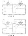
- FIG. 9Shown in FIG. 9 is semiconductor device structure 10 after growing SiGe layers of 52 and 54 epitaxially and in situ doped with p-type dopants, preferably boron, in openings 58 and 60 , respectively.
- p-type dopantspreferably boron
- the dopant concentrationincreases as the growth continues so that it is much more lightly doped at the interface with n-doped SiGe layers 62 and 64 than at the top surface.
- SiGe 12 layerpreferably has a germanium concentration of about 20 percent and the concentration of the grown SiGe layers 62 , 64 , 66 , and 68 are about 40 percent germanium.
- the lattice structure of SiGe layers 62 , 64 , 66 , and 68is compressive. SiGe layers 62 and 66 function as one stressor for transistor 20 , and layers 64 and 68 function as another stressor.
- FIG. 10Shown in FIG. 10 is semiconductor device structure 10 after performing an anneal that causes the dopants to move somewhat resulting in a P doped region 70 substantially in areas where silicon layer 14 and silicon layers 48 and 50 were present.
- the annealalso results in an N-doped regions 72 and 74 substantially where silicon regions 52 and 54 and source/drain extensions 26 and 28 were.
- the doping concentrationis higher away from the channel than adjacent to the channel, the region between N-doped regions 72 and 74 immediately under gate dielectric 24 .
- the annealfurther results in an N doped region 76 substantially in areas where silicon layer 14 and silicon layers 62 and 64 were present.
- the annealresults in an P-doped regions 78 and 80 substantially where SiGe layers 62 and 64 and source/drain extensions 36 and 38 were.
- the doping concentrationis higher away from the channel than adjacent to the channel, the region between P-doped regions 78 and 80 immediately under gate dielectric 34 .
- P channel region 70ensures the presence of a PN junction between the source/drain regions, N doped regions 72 and 74 , and the interface between silicon layer 14 and SiGe layer 12 .
- This interfaceboth on the side having transistor 18 and the side having transistor 20 , has many defects including at the corners of the interface. It is beneficial that these defects, including the ones in the corners, not interfere with source/drain operation which is achieved by virtue of the growth of N-doped layers 62 and 64 and P-doped layers 48 and 50 .
- this approachalso results in a silicon channel for the N channel transistor, which is the preferred material for N channel transistors.
Landscapes
- Insulated Gate Type Field-Effect Transistor (AREA)
Abstract
Description
- This invention relates to semiconductor devices and more particularly to semiconductor devices with stressors.
- P and N channel transistors have been found to have improved performance by use of strained semiconductor material in the channel. N channel transistors benefit from more tensile stress, whereas P channel transistors benefit from compressive stress. A number of techniques have been proposed to achieve one or both of these stresses. One of the difficulties is enhancing the stress for both the N and P channel transistors. Another issue is achieving an enhancing stress while not introducing detrimental defects. Another issue is providing the optimum direction for the stress. For example, P channel transistors benefit more from an increase in compressive in the channel length direction than from an increase in compressive stress in both the channel length and channel width direction. Another issue is proper material choices for the P and N channel devices. N channel devices are generally better if they have a silicon channel rather than a germanium or silicon germanium (SiGe) channel because SiGe has lower electron mobility than silicon.
- Thus, there is an need for a device that has the desired benefits that can be made in a process that improves on one or more of these issues.
- The foregoing and further and more specific objects and advantages of the invention will become readily apparent to those skilled in the art from the following detailed description of a preferred embodiment thereof taken in conjunction with the following drawings:
FIG. 1 is a cross section of a semiconductor device at a stage in a process that is according to an embodiment of the invention;FIG. 2 is a cross section of the semiconductor device at a stage in the process subsequent to that shown inFIG. 1 ;FIG. 3 is a cross section of the semiconductor device at a stage in the process subsequent to that shown inFIG. 2 ;FIG. 4 is a cross section of the semiconductor device at a stage in the process subsequent to that shown inFIG. 3 ;FIG. 5 is a cross section of the semiconductor device at a stage in the process subsequent to that shown inFIG. 4 ;FIG. 6 is a cross section of the semiconductor device at a stage in the process subsequent to that shown inFIG. 5 ; andFIG. 7 is a cross section of the semiconductor device at a stage in the process subsequent to that shown inFIG. 6 .FIG. 8 is a cross section of the semiconductor device at a stage in the process subsequent to that shown inFIG. 7 .FIG. 9 is a cross section of the semiconductor device at a stage in the process subsequent to that shown inFIG. 8 .FIG. 10 is a cross section of the semiconductor device at a stage in the process subsequent to that shown inFIG. 9 .- In one aspect a device structure has an N channel transistor with a silicon channel and stressors as the source/drains that result in tensile stress in the channel and a P channel transistor with a silicon channel and stressors as the source/drains that result in compressive stress in the channel. The stressors, silicon for the N channel transistor and SiGe with increased germanium concentration for the P channel transistor, are epitaxially grown from a SiGe layer. This is better understood by reference to the drawings and the following description.
- Shown in
FIG. 1 is asemiconductor device structure 10 having aSiGe layer 12 and asilicon layer 14 onSiGe layer 12.SiGe layer 12 is relaxed and has a concentration of about 20% germanium.Silicon layer 14 is also relaxed and is preferably pure silicon. UnderSiGe layer 12 is further structural support and in this case would preferably be an oxide layer and a relatively thick silicon layer. An alternative to this is to have a virtual silicon germanium substrate in whichSiGe layer 12 is grown from an underlying silicon layer with a gradient in a manner that results inSiGe layer 12 having relaxed strain. The structure shown inFIG. 1 is believed to be unique in combining relaxed silicon and relaxed SiGe as two layers bonded together, but it can be made using known techniques. A wafer having a relaxed SiGe layer on its top face and another wafer having a relaxed silicon layer on its top face can be bonded together face to face so that the SiGe and silicon layers are bonded together. A subsequent cleaving of the silicon layer will result indevice structure 10 ofFIG. 1 . A hydrogen implant along the line of cleaving is one way to assist in providing the cleaving to leave the desired thickness of the silicon layer. Another technique that could be used to provide a similar structure is to that ofFIG. 1 is to provide an underlying relaxed SiGe layer, epitaxially growing a graded layer that ends in pure silicon, and then continuing to grow a pure silicon layer that would be relaxed. Epitaxially growing a relaxed a silicon layer on a SiGe layer is known to be achievable by reducing the concentration of germanium during the growth. The substrate material shown inFIG. 1 is based on a semiconductor wafer having a first semiconductor layer,SiGe layer 12, substantially consisting of silicon and germanium, wherein the first semiconductor layer has relaxed strain, and a second semiconductor layer on the first semiconductor layer substantially consisting of silicon,silicon layer 14, wherein the second semiconductor layer has relaxed strain. - Shown in
FIG. 2 issemiconductor device structure 10 after forming anisolation region 16 insilicon layer 14 andSiGe layer 12. Processes for forming isolation regions such asisolation region 16 are well known. Any such process should be satisfactory. - Shown in
FIG. 3 issemiconductor device structure 10 after forming anN channel transistor 18 on one side ofisolation region 16 and aP channel transistor 20 on the other side ofisolation region 16. Prior totransistors transistor 18 is implanted with p-type dopants, preferably boron, to provide background doping, and the side withtransistor 20 is implanted with n-type dopants, preferably phosphorus and/or arsenic, to provide background doping.Transistor 18 comprises agate 22 oversilicon layer 14, agate dielectric 24 onsilicon layer 14 and undergate 22, a source/drain extension 26 insilicon layer 14 on one side ofgate 22, a source/drain extension 28 insilicon layer 14 on the other side ofgate 22, and asidewall spacer 30 aroundgate 22.Transistor 20 comprises agate 32 oversilicon layer 14, agate dielectric 34 onsilicon layer 14 and undergate 22, a source/drain extension 26 insilicon layer 14 on one side ofgate 22 and a source/drain 30extension 28 insilicon layer 14 on the other side ofgate 22. Source/drain extensions - Shown in
FIG. 4 issemiconductor device structure 10 after masking the side withtransistor 20 with ahard mask 42 of oxide andetching openings silicon layer 14 and intoSiGe layer 12 about 500 Angstroms. This etch usesgate 22 andsidewall spacer 30 as a mask so thatopenings gate 22. The etch exposesSiGe layer 12 inopenings drain extensions sidewall spacer 30 andsilicon layer 14 undergate 22 andsidewall spacer 30. - Shown in
FIG. 5 issemiconductor device structure 10 after growing silicon layers of48 and50 epitaxially and in situ doped with p-type dopants, preferably boron, inopenings SiGe layer 12 and exposed sides ofsilicon layer 14. P-doped silicon layers follow the lattice from which they grow so that alongsilicon layer 14 it is relatively relaxed but alongSiGe layer 12 it is tensile. - Shown in
FIG. 6 issemiconductor device structure 10 after growing silicon layers of52 and54 epitaxially and in situ doped with n-type dopants, preferably arsenic and/or phosphorus, inopenings SiGe layer 12 and the relaxed condition ofsemiconductor layer 14. Silicon layers48 and52 function as one stressor fortransistor 18, and layers50 and54 function as another stressor. - Shown in
FIG. 7 issemiconductor device structure 10 after masking the side withtransistor 18 with ahard mask 56 of oxide andetching openings silicon layer 14 and intoSiGe layer 12 about 500 Angstroms. This etch usesgate 32 andsidewall spacer 40 as a mask so thatopenings gate 32. The etch exposesSiGe layer 12 inopenings drain extensions sidewall spacer 40 andsilicon layer 14 undergate 32 andsidewall spacer 40. - Shown in
FIG. 8 issemiconductor device structure 10 after growing SiGe layers of62 and64 epitaxially and in situ doped with n-type dopants, preferably arsenic and/or phosphorus, inopenings SiGe layer 12. N-doped SiGe layers62 and64 grow on the exposed surface ofSiGe layer 12 and exposed sides ofsilicon layer 14 and follow the lattice from which they grow. Thus, the portions alongSiGe layer 12 are tensile laterally in the direction of current flow of transistor20 (channel length direction), which is the primary direction of interest. The SiGe growth on the sides ofsemiconductor layer 14 is also compressive but minimally so in the channel length direction. - Shown in
FIG. 9 issemiconductor device structure 10 after growing SiGe layers of52 and54 epitaxially and in situ doped with p-type dopants, preferably boron, inopenings SiGe 12 layer preferably has a germanium concentration of about 20 percent and the concentration of the grown SiGe layers62,64,66, and68 are about 40 percent germanium. The lattice structure of SiGe layers62,64,66, and68 is compressive. SiGe layers62 and66 function as one stressor fortransistor 20, and layers64 and68 function as another stressor. - Shown in
FIG. 10 issemiconductor device structure 10 after performing an anneal that causes the dopants to move somewhat resulting in a P dopedregion 70 substantially in areas wheresilicon layer 14 andsilicon layers regions silicon regions drain extensions regions gate dielectric 24. The anneal further results in an N dopedregion 76 substantially in areas wheresilicon layer 14 andsilicon layers regions drain extensions regions gate dielectric 34. P channel region 70 ensures the presence of a PN junction between the source/drain regions, N dopedregions silicon layer 14 andSiGe layer 12. This interface, both on theside having transistor 18 and theside having transistor 20, has many defects including at the corners of the interface. It is beneficial that these defects, including the ones in the corners, not interfere with source/drain operation which is achieved by virtue of the growth of N-dopedlayers layers - Various other changes and modifications to the embodiments herein chosen for purposes of illustration will readily occur to those skilled in the art. For example, the isolation regions were described as using an existing process, but the isolation regions could be made using a process that is subsequently developed. In come cases particular thicknesses were described but other thicknesses may be beneficial. To the extent that such modifications and variations do not depart from the spirit of the invention, they are intended to be included within the scope thereof which is assessed only by a fair interpretation of the following claims.
Claims (21)
Priority Applications (1)
| Application Number | Priority Date | Filing Date | Title |
|---|---|---|---|
| US11/373,536US7479422B2 (en) | 2006-03-10 | 2006-03-10 | Semiconductor device with stressors and method therefor |
Applications Claiming Priority (1)
| Application Number | Priority Date | Filing Date | Title |
|---|---|---|---|
| US11/373,536US7479422B2 (en) | 2006-03-10 | 2006-03-10 | Semiconductor device with stressors and method therefor |
Publications (2)
| Publication Number | Publication Date |
|---|---|
| US20070210314A1true US20070210314A1 (en) | 2007-09-13 |
| US7479422B2 US7479422B2 (en) | 2009-01-20 |
Family
ID=38478026
Family Applications (1)
| Application Number | Title | Priority Date | Filing Date |
|---|---|---|---|
| US11/373,536Expired - Fee RelatedUS7479422B2 (en) | 2006-03-10 | 2006-03-10 | Semiconductor device with stressors and method therefor |
Country Status (1)
| Country | Link |
|---|---|
| US (1) | US7479422B2 (en) |
Cited By (4)
| Publication number | Priority date | Publication date | Assignee | Title |
|---|---|---|---|---|
| US20070235802A1 (en)* | 2006-04-05 | 2007-10-11 | Chartered Semiconductor Manufacturing Ltd | Method to control source/drain stressor profiles for stress engineering |
| US20080179627A1 (en)* | 2007-01-31 | 2008-07-31 | Meikei Ieong | Strained MOS devices using source/drain epitaxy |
| US20100219475A1 (en)* | 2009-02-27 | 2010-09-02 | Stephan Kronholz | Integration of semiconductor alloys in pmos and nmos transistors by using a common cavity etch process |
| US20120305995A1 (en)* | 2011-05-30 | 2012-12-06 | Globalfoundries Inc. | Performance enhancement in transistors by providing an embedded strain-inducing semiconductor material on the basis of a seed layer |
Families Citing this family (1)
| Publication number | Priority date | Publication date | Assignee | Title |
|---|---|---|---|---|
| CN105097554B (en)* | 2015-08-24 | 2018-12-07 | 上海华力微电子有限公司 | For reducing the method and system of the dislocation defects in high concentration epitaxy technique |
Citations (10)
| Publication number | Priority date | Publication date | Assignee | Title |
|---|---|---|---|---|
| US6429061B1 (en)* | 2000-07-26 | 2002-08-06 | International Business Machines Corporation | Method to fabricate a strained Si CMOS structure using selective epitaxial deposition of Si after device isolation formation |
| US6831350B1 (en)* | 2003-10-02 | 2004-12-14 | Freescale Semiconductor, Inc. | Semiconductor structure with different lattice constant materials and method for forming the same |
| US6838728B2 (en)* | 2001-08-09 | 2005-01-04 | Amberwave Systems Corporation | Buried-channel devices and substrates for fabrication of semiconductor-based devices |
| US6885084B2 (en)* | 2001-11-01 | 2005-04-26 | Intel Corporation | Semiconductor transistor having a stressed channel |
| US6887762B1 (en)* | 1998-11-12 | 2005-05-03 | Intel Corporation | Method of fabricating a field effect transistor structure with abrupt source/drain junctions |
| US20050242340A1 (en)* | 2004-03-23 | 2005-11-03 | International Business Machines Corporation | Strained silicon NMOS devices with embedded source/drain |
| US20060205167A1 (en)* | 2005-03-11 | 2006-09-14 | Jack Kavalieros | Complementary metal oxide semiconductor integrated circuit using uniaxial compressive stress and biaxial compressive stress |
| US7230264B2 (en)* | 2004-08-24 | 2007-06-12 | Freescale Semiconductor, Inc. | Semiconductor transistor having structural elements of differing materials |
| US7268049B2 (en)* | 2004-09-30 | 2007-09-11 | International Business Machines Corporation | Structure and method for manufacturing MOSFET with super-steep retrograded island |
| US7288448B2 (en)* | 2004-08-24 | 2007-10-30 | Orlowski Marius K | Method and apparatus for mobility enhancement in a semiconductor device |
- 2006
- 2006-03-10USUS11/373,536patent/US7479422B2/ennot_activeExpired - Fee Related
Patent Citations (10)
| Publication number | Priority date | Publication date | Assignee | Title |
|---|---|---|---|---|
| US6887762B1 (en)* | 1998-11-12 | 2005-05-03 | Intel Corporation | Method of fabricating a field effect transistor structure with abrupt source/drain junctions |
| US6429061B1 (en)* | 2000-07-26 | 2002-08-06 | International Business Machines Corporation | Method to fabricate a strained Si CMOS structure using selective epitaxial deposition of Si after device isolation formation |
| US6838728B2 (en)* | 2001-08-09 | 2005-01-04 | Amberwave Systems Corporation | Buried-channel devices and substrates for fabrication of semiconductor-based devices |
| US6885084B2 (en)* | 2001-11-01 | 2005-04-26 | Intel Corporation | Semiconductor transistor having a stressed channel |
| US6831350B1 (en)* | 2003-10-02 | 2004-12-14 | Freescale Semiconductor, Inc. | Semiconductor structure with different lattice constant materials and method for forming the same |
| US20050242340A1 (en)* | 2004-03-23 | 2005-11-03 | International Business Machines Corporation | Strained silicon NMOS devices with embedded source/drain |
| US7230264B2 (en)* | 2004-08-24 | 2007-06-12 | Freescale Semiconductor, Inc. | Semiconductor transistor having structural elements of differing materials |
| US7288448B2 (en)* | 2004-08-24 | 2007-10-30 | Orlowski Marius K | Method and apparatus for mobility enhancement in a semiconductor device |
| US7268049B2 (en)* | 2004-09-30 | 2007-09-11 | International Business Machines Corporation | Structure and method for manufacturing MOSFET with super-steep retrograded island |
| US20060205167A1 (en)* | 2005-03-11 | 2006-09-14 | Jack Kavalieros | Complementary metal oxide semiconductor integrated circuit using uniaxial compressive stress and biaxial compressive stress |
Cited By (10)
| Publication number | Priority date | Publication date | Assignee | Title |
|---|---|---|---|---|
| US20070235802A1 (en)* | 2006-04-05 | 2007-10-11 | Chartered Semiconductor Manufacturing Ltd | Method to control source/drain stressor profiles for stress engineering |
| US8017487B2 (en)* | 2006-04-05 | 2011-09-13 | Globalfoundries Singapore Pte. Ltd. | Method to control source/drain stressor profiles for stress engineering |
| US8450775B2 (en) | 2006-04-05 | 2013-05-28 | Globalfoundries Singapore Pte. Ltd. | Method to control source/drain stressor profiles for stress engineering |
| US20080179627A1 (en)* | 2007-01-31 | 2008-07-31 | Meikei Ieong | Strained MOS devices using source/drain epitaxy |
| US7525161B2 (en)* | 2007-01-31 | 2009-04-28 | International Business Machines Corporation | Strained MOS devices using source/drain epitaxy |
| US20100219475A1 (en)* | 2009-02-27 | 2010-09-02 | Stephan Kronholz | Integration of semiconductor alloys in pmos and nmos transistors by using a common cavity etch process |
| US9269631B2 (en)* | 2009-02-27 | 2016-02-23 | Advance Micro Devices, Inc. | Integration of semiconductor alloys in PMOS and NMOS transistors by using a common cavity etch process |
| US20120305995A1 (en)* | 2011-05-30 | 2012-12-06 | Globalfoundries Inc. | Performance enhancement in transistors by providing an embedded strain-inducing semiconductor material on the basis of a seed layer |
| US9224863B2 (en)* | 2011-05-30 | 2015-12-29 | Globalfoundries Inc. | Performance enhancement in transistors by providing an embedded strain-inducing semiconductor material on the basis of a seed layer |
| US9484459B2 (en) | 2011-05-30 | 2016-11-01 | Globalfoundries Inc. | Performance enhancement in transistors by providing an embedded strain-inducing semiconductor material on the basis of a seed layer |
Also Published As
| Publication number | Publication date |
|---|---|
| US7479422B2 (en) | 2009-01-20 |
Similar Documents
| Publication | Publication Date | Title |
|---|---|---|
| JP5043314B2 (en) | Method for fabricating strained P-type MOSFET with graded embedded silicon-germanium source-drain and / or extension | |
| US7176481B2 (en) | In situ doped embedded sige extension and source/drain for enhanced PFET performance | |
| US7446350B2 (en) | Embedded silicon germanium using a double buried oxide silicon-on-insulator wafer | |
| US8912567B2 (en) | Strained channel transistor and method of fabrication thereof | |
| US7605407B2 (en) | Composite stressors with variable element atomic concentrations in MOS devices | |
| US6831292B2 (en) | Semiconductor structures employing strained material layers with defined impurity gradients and methods for fabricating same | |
| US7781799B2 (en) | Source/drain strained layers | |
| US7682887B2 (en) | Transistor having high mobility channel and methods | |
| US8120065B2 (en) | Tensile strained NMOS transistor using group III-N source/drain regions | |
| US8344447B2 (en) | Silicon layer for stopping dislocation propagation | |
| US8278179B2 (en) | LDD epitaxy for FinFETs | |
| US7572706B2 (en) | Source/drain stressor and method therefor | |
| US8183640B2 (en) | Method of fabricating transistors and a transistor structure for improving short channel effect and drain induced barrier lowering | |
| US8329550B2 (en) | Method of fabricating transistor for semiconductor device | |
| JP2007294707A (en) | Semiconductor device manufacturing method and semiconductor device | |
| US20080054250A1 (en) | Structure and methods for forming SiGe stressors | |
| US20080116487A1 (en) | Methods of fabricating transistors having high carrier mobility and transistors fabricated thereby | |
| US7479422B2 (en) | Semiconductor device with stressors and method therefor | |
| US8440539B2 (en) | Isolation trench processing for strain control | |
| JP2009016423A (en) | Semiconductor device and manufacturing method thereof |
Legal Events
| Date | Code | Title | Description |
|---|---|---|---|
| AS | Assignment | Owner name:FREESCALE SEMICONDUCTOR, INC., TEXAS Free format text:ASSIGNMENT OF ASSIGNORS INTEREST;ASSIGNORS:WINSTEAD, BRIAN A.;WHITE, TED R.;ZHANG, DA;REEL/FRAME:017698/0286 Effective date:20060310 | |
| AS | Assignment | Owner name:CITIBANK, N.A. AS COLLATERAL AGENT, NEW YORK Free format text:SECURITY AGREEMENT;ASSIGNORS:FREESCALE SEMICONDUCTOR, INC.;FREESCALE ACQUISITION CORPORATION;FREESCALE ACQUISITION HOLDINGS CORP.;AND OTHERS;REEL/FRAME:018855/0129 Effective date:20061201 Owner name:CITIBANK, N.A. AS COLLATERAL AGENT,NEW YORK Free format text:SECURITY AGREEMENT;ASSIGNORS:FREESCALE SEMICONDUCTOR, INC.;FREESCALE ACQUISITION CORPORATION;FREESCALE ACQUISITION HOLDINGS CORP.;AND OTHERS;REEL/FRAME:018855/0129 Effective date:20061201 | |
| STCF | Information on status: patent grant | Free format text:PATENTED CASE | |
| AS | Assignment | Owner name:CITIBANK, N.A., NEW YORK Free format text:SECURITY AGREEMENT;ASSIGNOR:FREESCALE SEMICONDUCTOR, INC.;REEL/FRAME:022703/0405 Effective date:20090428 Owner name:CITIBANK, N.A.,NEW YORK Free format text:SECURITY AGREEMENT;ASSIGNOR:FREESCALE SEMICONDUCTOR, INC.;REEL/FRAME:022703/0405 Effective date:20090428 | |
| AS | Assignment | Owner name:CITIBANK, N.A., AS COLLATERAL AGENT,NEW YORK Free format text:SECURITY AGREEMENT;ASSIGNOR:FREESCALE SEMICONDUCTOR, INC.;REEL/FRAME:024397/0001 Effective date:20100413 Owner name:CITIBANK, N.A., AS COLLATERAL AGENT, NEW YORK Free format text:SECURITY AGREEMENT;ASSIGNOR:FREESCALE SEMICONDUCTOR, INC.;REEL/FRAME:024397/0001 Effective date:20100413 | |
| FPAY | Fee payment | Year of fee payment:4 | |
| AS | Assignment | Owner name:CITIBANK, N.A., AS NOTES COLLATERAL AGENT, NEW YORK Free format text:SECURITY AGREEMENT;ASSIGNOR:FREESCALE SEMICONDUCTOR, INC.;REEL/FRAME:030633/0424 Effective date:20130521 Owner name:CITIBANK, N.A., AS NOTES COLLATERAL AGENT, NEW YOR Free format text:SECURITY AGREEMENT;ASSIGNOR:FREESCALE SEMICONDUCTOR, INC.;REEL/FRAME:030633/0424 Effective date:20130521 | |
| AS | Assignment | Owner name:CITIBANK, N.A., AS NOTES COLLATERAL AGENT, NEW YORK Free format text:SECURITY AGREEMENT;ASSIGNOR:FREESCALE SEMICONDUCTOR, INC.;REEL/FRAME:031591/0266 Effective date:20131101 Owner name:CITIBANK, N.A., AS NOTES COLLATERAL AGENT, NEW YOR Free format text:SECURITY AGREEMENT;ASSIGNOR:FREESCALE SEMICONDUCTOR, INC.;REEL/FRAME:031591/0266 Effective date:20131101 | |
| AS | Assignment | Owner name:FREESCALE SEMICONDUCTOR, INC., TEXAS Free format text:PATENT RELEASE;ASSIGNOR:CITIBANK, N.A., AS COLLATERAL AGENT;REEL/FRAME:037354/0793 Effective date:20151207 Owner name:FREESCALE SEMICONDUCTOR, INC., TEXAS Free format text:PATENT RELEASE;ASSIGNOR:CITIBANK, N.A., AS COLLATERAL AGENT;REEL/FRAME:037354/0225 Effective date:20151207 Owner name:FREESCALE SEMICONDUCTOR, INC., TEXAS Free format text:PATENT RELEASE;ASSIGNOR:CITIBANK, N.A., AS COLLATERAL AGENT;REEL/FRAME:037356/0553 Effective date:20151207 Owner name:FREESCALE SEMICONDUCTOR, INC., TEXAS Free format text:PATENT RELEASE;ASSIGNOR:CITIBANK, N.A., AS COLLATERAL AGENT;REEL/FRAME:037356/0143 Effective date:20151207 | |
| AS | Assignment | Owner name:MORGAN STANLEY SENIOR FUNDING, INC., MARYLAND Free format text:ASSIGNMENT AND ASSUMPTION OF SECURITY INTEREST IN PATENTS;ASSIGNOR:CITIBANK, N.A.;REEL/FRAME:037486/0517 Effective date:20151207 | |
| AS | Assignment | Owner name:MORGAN STANLEY SENIOR FUNDING, INC., MARYLAND Free format text:ASSIGNMENT AND ASSUMPTION OF SECURITY INTEREST IN PATENTS;ASSIGNOR:CITIBANK, N.A.;REEL/FRAME:037518/0292 Effective date:20151207 | |
| FPAY | Fee payment | Year of fee payment:8 | |
| AS | Assignment | Owner name:MORGAN STANLEY SENIOR FUNDING, INC., MARYLAND Free format text:SUPPLEMENT TO THE SECURITY AGREEMENT;ASSIGNOR:FREESCALE SEMICONDUCTOR, INC.;REEL/FRAME:039138/0001 Effective date:20160525 | |
| AS | Assignment | Owner name:NXP, B.V., F/K/A FREESCALE SEMICONDUCTOR, INC., NETHERLANDS Free format text:RELEASE BY SECURED PARTY;ASSIGNOR:MORGAN STANLEY SENIOR FUNDING, INC.;REEL/FRAME:040925/0001 Effective date:20160912 Owner name:NXP, B.V., F/K/A FREESCALE SEMICONDUCTOR, INC., NE Free format text:RELEASE BY SECURED PARTY;ASSIGNOR:MORGAN STANLEY SENIOR FUNDING, INC.;REEL/FRAME:040925/0001 Effective date:20160912 | |
| AS | Assignment | Owner name:NXP B.V., NETHERLANDS Free format text:RELEASE BY SECURED PARTY;ASSIGNOR:MORGAN STANLEY SENIOR FUNDING, INC.;REEL/FRAME:040928/0001 Effective date:20160622 | |
| AS | Assignment | Owner name:NXP USA, INC., TEXAS Free format text:CHANGE OF NAME;ASSIGNOR:FREESCALE SEMICONDUCTOR, INC.;REEL/FRAME:040632/0001 Effective date:20161107 | |
| AS | Assignment | Owner name:MORGAN STANLEY SENIOR FUNDING, INC., MARYLAND Free format text:CORRECTIVE ASSIGNMENT TO CORRECT THE REMOVE PATENTS 8108266 AND 8062324 AND REPLACE THEM WITH 6108266 AND 8060324 PREVIOUSLY RECORDED ON REEL 037518 FRAME 0292. ASSIGNOR(S) HEREBY CONFIRMS THE ASSIGNMENT AND ASSUMPTION OF SECURITY INTEREST IN PATENTS;ASSIGNOR:CITIBANK, N.A.;REEL/FRAME:041703/0536 Effective date:20151207 | |
| AS | Assignment | Owner name:NXP USA, INC., TEXAS Free format text:CORRECTIVE ASSIGNMENT TO CORRECT THE NATURE OF CONVEYANCE PREVIOUSLY RECORDED AT REEL: 040632 FRAME: 0001. ASSIGNOR(S) HEREBY CONFIRMS THE MERGER AND CHANGE OF NAME;ASSIGNOR:FREESCALE SEMICONDUCTOR INC.;REEL/FRAME:044209/0047 Effective date:20161107 | |
| AS | Assignment | Owner name:SHENZHEN XINGUODU TECHNOLOGY CO., LTD., CHINA Free format text:CORRECTIVE ASSIGNMENT TO CORRECT THE TO CORRECT THE APPLICATION NO. FROM 13,883,290 TO 13,833,290 PREVIOUSLY RECORDED ON REEL 041703 FRAME 0536. ASSIGNOR(S) HEREBY CONFIRMS THE THE ASSIGNMENT AND ASSUMPTION OF SECURITYINTEREST IN PATENTS.;ASSIGNOR:MORGAN STANLEY SENIOR FUNDING, INC.;REEL/FRAME:048734/0001 Effective date:20190217 | |
| AS | Assignment | Owner name:NXP B.V., NETHERLANDS Free format text:RELEASE BY SECURED PARTY;ASSIGNOR:MORGAN STANLEY SENIOR FUNDING, INC.;REEL/FRAME:050744/0097 Effective date:20190903 | |
| AS | Assignment | Owner name:MORGAN STANLEY SENIOR FUNDING, INC., MARYLAND Free format text:CORRECTIVE ASSIGNMENT TO CORRECT THE REMOVE APPLICATION11759915 AND REPLACE IT WITH APPLICATION 11759935 PREVIOUSLY RECORDED ON REEL 037486 FRAME 0517. ASSIGNOR(S) HEREBY CONFIRMS THE ASSIGNMENT AND ASSUMPTION OF SECURITYINTEREST IN PATENTS;ASSIGNOR:CITIBANK, N.A.;REEL/FRAME:053547/0421 Effective date:20151207 | |
| AS | Assignment | Owner name:NXP B.V., NETHERLANDS Free format text:CORRECTIVE ASSIGNMENT TO CORRECT THE REMOVEAPPLICATION 11759915 AND REPLACE IT WITH APPLICATION11759935 PREVIOUSLY RECORDED ON REEL 040928 FRAME 0001. ASSIGNOR(S) HEREBY CONFIRMS THE RELEASE OF SECURITYINTEREST;ASSIGNOR:MORGAN STANLEY SENIOR FUNDING, INC.;REEL/FRAME:052915/0001 Effective date:20160622 | |
| AS | Assignment | Owner name:NXP, B.V. F/K/A FREESCALE SEMICONDUCTOR, INC., NETHERLANDS Free format text:CORRECTIVE ASSIGNMENT TO CORRECT THE REMOVEAPPLICATION 11759915 AND REPLACE IT WITH APPLICATION11759935 PREVIOUSLY RECORDED ON REEL 040925 FRAME 0001. ASSIGNOR(S) HEREBY CONFIRMS THE RELEASE OF SECURITYINTEREST;ASSIGNOR:MORGAN STANLEY SENIOR FUNDING, INC.;REEL/FRAME:052917/0001 Effective date:20160912 | |
| FEPP | Fee payment procedure | Free format text:MAINTENANCE FEE REMINDER MAILED (ORIGINAL EVENT CODE: REM.); ENTITY STATUS OF PATENT OWNER: LARGE ENTITY | |
| LAPS | Lapse for failure to pay maintenance fees | Free format text:PATENT EXPIRED FOR FAILURE TO PAY MAINTENANCE FEES (ORIGINAL EVENT CODE: EXP.); ENTITY STATUS OF PATENT OWNER: LARGE ENTITY | |
| STCH | Information on status: patent discontinuation | Free format text:PATENT EXPIRED DUE TO NONPAYMENT OF MAINTENANCE FEES UNDER 37 CFR 1.362 | |
| FP | Lapsed due to failure to pay maintenance fee | Effective date:20210120 |