US20070206145A1 - Liquid crystal display having particular electrodes and particular common line - Google Patents
Liquid crystal display having particular electrodes and particular common lineDownload PDFInfo
- Publication number
- US20070206145A1 US20070206145A1US11/797,319US79731907AUS2007206145A1US 20070206145 A1US20070206145 A1US 20070206145A1US 79731907 AUS79731907 AUS 79731907AUS 2007206145 A1US2007206145 A1US 2007206145A1
- Authority
- US
- United States
- Prior art keywords
- liquid crystal
- crystal display
- spacer
- pixel
- view
- Prior art date
- Legal status (The legal status is an assumption and is not a legal conclusion. Google has not performed a legal analysis and makes no representation as to the accuracy of the status listed.)
- Granted
Links
Images


Classifications
- G—PHYSICS
- G02—OPTICS
- G02F—OPTICAL DEVICES OR ARRANGEMENTS FOR THE CONTROL OF LIGHT BY MODIFICATION OF THE OPTICAL PROPERTIES OF THE MEDIA OF THE ELEMENTS INVOLVED THEREIN; NON-LINEAR OPTICS; FREQUENCY-CHANGING OF LIGHT; OPTICAL LOGIC ELEMENTS; OPTICAL ANALOGUE/DIGITAL CONVERTERS
- G02F1/00—Devices or arrangements for the control of the intensity, colour, phase, polarisation or direction of light arriving from an independent light source, e.g. switching, gating or modulating; Non-linear optics
- G02F1/01—Devices or arrangements for the control of the intensity, colour, phase, polarisation or direction of light arriving from an independent light source, e.g. switching, gating or modulating; Non-linear optics for the control of the intensity, phase, polarisation or colour
- G02F1/13—Devices or arrangements for the control of the intensity, colour, phase, polarisation or direction of light arriving from an independent light source, e.g. switching, gating or modulating; Non-linear optics for the control of the intensity, phase, polarisation or colour based on liquid crystals, e.g. single liquid crystal display cells
- G02F1/133—Constructional arrangements; Operation of liquid crystal cells; Circuit arrangements
- G02F1/136—Liquid crystal cells structurally associated with a semi-conducting layer or substrate, e.g. cells forming part of an integrated circuit
- G—PHYSICS
- G02—OPTICS
- G02F—OPTICAL DEVICES OR ARRANGEMENTS FOR THE CONTROL OF LIGHT BY MODIFICATION OF THE OPTICAL PROPERTIES OF THE MEDIA OF THE ELEMENTS INVOLVED THEREIN; NON-LINEAR OPTICS; FREQUENCY-CHANGING OF LIGHT; OPTICAL LOGIC ELEMENTS; OPTICAL ANALOGUE/DIGITAL CONVERTERS
- G02F1/00—Devices or arrangements for the control of the intensity, colour, phase, polarisation or direction of light arriving from an independent light source, e.g. switching, gating or modulating; Non-linear optics
- G02F1/01—Devices or arrangements for the control of the intensity, colour, phase, polarisation or direction of light arriving from an independent light source, e.g. switching, gating or modulating; Non-linear optics for the control of the intensity, phase, polarisation or colour
- G02F1/13—Devices or arrangements for the control of the intensity, colour, phase, polarisation or direction of light arriving from an independent light source, e.g. switching, gating or modulating; Non-linear optics for the control of the intensity, phase, polarisation or colour based on liquid crystals, e.g. single liquid crystal display cells
- G02F1/133—Constructional arrangements; Operation of liquid crystal cells; Circuit arrangements
- G02F1/1333—Constructional arrangements; Manufacturing methods
- G02F1/1343—Electrodes
- G02F1/134309—Electrodes characterised by their geometrical arrangement
- G02F1/134363—Electrodes characterised by their geometrical arrangement for applying an electric field parallel to the substrate, i.e. in-plane switching [IPS]
- G—PHYSICS
- G02—OPTICS
- G02F—OPTICAL DEVICES OR ARRANGEMENTS FOR THE CONTROL OF LIGHT BY MODIFICATION OF THE OPTICAL PROPERTIES OF THE MEDIA OF THE ELEMENTS INVOLVED THEREIN; NON-LINEAR OPTICS; FREQUENCY-CHANGING OF LIGHT; OPTICAL LOGIC ELEMENTS; OPTICAL ANALOGUE/DIGITAL CONVERTERS
- G02F1/00—Devices or arrangements for the control of the intensity, colour, phase, polarisation or direction of light arriving from an independent light source, e.g. switching, gating or modulating; Non-linear optics
- G02F1/01—Devices or arrangements for the control of the intensity, colour, phase, polarisation or direction of light arriving from an independent light source, e.g. switching, gating or modulating; Non-linear optics for the control of the intensity, phase, polarisation or colour
- G02F1/13—Devices or arrangements for the control of the intensity, colour, phase, polarisation or direction of light arriving from an independent light source, e.g. switching, gating or modulating; Non-linear optics for the control of the intensity, phase, polarisation or colour based on liquid crystals, e.g. single liquid crystal display cells
- G02F1/1303—Apparatus specially adapted to the manufacture of LCDs
- G—PHYSICS
- G02—OPTICS
- G02F—OPTICAL DEVICES OR ARRANGEMENTS FOR THE CONTROL OF LIGHT BY MODIFICATION OF THE OPTICAL PROPERTIES OF THE MEDIA OF THE ELEMENTS INVOLVED THEREIN; NON-LINEAR OPTICS; FREQUENCY-CHANGING OF LIGHT; OPTICAL LOGIC ELEMENTS; OPTICAL ANALOGUE/DIGITAL CONVERTERS
- G02F1/00—Devices or arrangements for the control of the intensity, colour, phase, polarisation or direction of light arriving from an independent light source, e.g. switching, gating or modulating; Non-linear optics
- G02F1/01—Devices or arrangements for the control of the intensity, colour, phase, polarisation or direction of light arriving from an independent light source, e.g. switching, gating or modulating; Non-linear optics for the control of the intensity, phase, polarisation or colour
- G02F1/13—Devices or arrangements for the control of the intensity, colour, phase, polarisation or direction of light arriving from an independent light source, e.g. switching, gating or modulating; Non-linear optics for the control of the intensity, phase, polarisation or colour based on liquid crystals, e.g. single liquid crystal display cells
- G02F1/133—Constructional arrangements; Operation of liquid crystal cells; Circuit arrangements
- G02F1/1333—Constructional arrangements; Manufacturing methods
- G02F1/1339—Gaskets; Spacers; Sealing of cells
- G02F1/13394—Gaskets; Spacers; Sealing of cells spacers regularly patterned on the cell subtrate, e.g. walls, pillars
- G—PHYSICS
- G02—OPTICS
- G02F—OPTICAL DEVICES OR ARRANGEMENTS FOR THE CONTROL OF LIGHT BY MODIFICATION OF THE OPTICAL PROPERTIES OF THE MEDIA OF THE ELEMENTS INVOLVED THEREIN; NON-LINEAR OPTICS; FREQUENCY-CHANGING OF LIGHT; OPTICAL LOGIC ELEMENTS; OPTICAL ANALOGUE/DIGITAL CONVERTERS
- G02F1/00—Devices or arrangements for the control of the intensity, colour, phase, polarisation or direction of light arriving from an independent light source, e.g. switching, gating or modulating; Non-linear optics
- G02F1/01—Devices or arrangements for the control of the intensity, colour, phase, polarisation or direction of light arriving from an independent light source, e.g. switching, gating or modulating; Non-linear optics for the control of the intensity, phase, polarisation or colour
- G02F1/13—Devices or arrangements for the control of the intensity, colour, phase, polarisation or direction of light arriving from an independent light source, e.g. switching, gating or modulating; Non-linear optics for the control of the intensity, phase, polarisation or colour based on liquid crystals, e.g. single liquid crystal display cells
- G02F1/133—Constructional arrangements; Operation of liquid crystal cells; Circuit arrangements
- G02F1/1333—Constructional arrangements; Manufacturing methods
- G02F1/1335—Structural association of cells with optical devices, e.g. polarisers or reflectors
- G02F1/133509—Filters, e.g. light shielding masks
- G02F1/133512—Light shielding layers, e.g. black matrix
- G—PHYSICS
- G02—OPTICS
- G02F—OPTICAL DEVICES OR ARRANGEMENTS FOR THE CONTROL OF LIGHT BY MODIFICATION OF THE OPTICAL PROPERTIES OF THE MEDIA OF THE ELEMENTS INVOLVED THEREIN; NON-LINEAR OPTICS; FREQUENCY-CHANGING OF LIGHT; OPTICAL LOGIC ELEMENTS; OPTICAL ANALOGUE/DIGITAL CONVERTERS
- G02F1/00—Devices or arrangements for the control of the intensity, colour, phase, polarisation or direction of light arriving from an independent light source, e.g. switching, gating or modulating; Non-linear optics
- G02F1/01—Devices or arrangements for the control of the intensity, colour, phase, polarisation or direction of light arriving from an independent light source, e.g. switching, gating or modulating; Non-linear optics for the control of the intensity, phase, polarisation or colour
- G02F1/13—Devices or arrangements for the control of the intensity, colour, phase, polarisation or direction of light arriving from an independent light source, e.g. switching, gating or modulating; Non-linear optics for the control of the intensity, phase, polarisation or colour based on liquid crystals, e.g. single liquid crystal display cells
- G02F1/133—Constructional arrangements; Operation of liquid crystal cells; Circuit arrangements
- G02F1/1333—Constructional arrangements; Manufacturing methods
- G02F1/1339—Gaskets; Spacers; Sealing of cells
- G—PHYSICS
- G02—OPTICS
- G02F—OPTICAL DEVICES OR ARRANGEMENTS FOR THE CONTROL OF LIGHT BY MODIFICATION OF THE OPTICAL PROPERTIES OF THE MEDIA OF THE ELEMENTS INVOLVED THEREIN; NON-LINEAR OPTICS; FREQUENCY-CHANGING OF LIGHT; OPTICAL LOGIC ELEMENTS; OPTICAL ANALOGUE/DIGITAL CONVERTERS
- G02F2201/00—Constructional arrangements not provided for in groups G02F1/00 - G02F7/00
- G02F2201/40—Arrangements for improving the aperture ratio
- G—PHYSICS
- G02—OPTICS
- G02F—OPTICAL DEVICES OR ARRANGEMENTS FOR THE CONTROL OF LIGHT BY MODIFICATION OF THE OPTICAL PROPERTIES OF THE MEDIA OF THE ELEMENTS INVOLVED THEREIN; NON-LINEAR OPTICS; FREQUENCY-CHANGING OF LIGHT; OPTICAL LOGIC ELEMENTS; OPTICAL ANALOGUE/DIGITAL CONVERTERS
- G02F2202/00—Materials and properties
- G02F2202/28—Adhesive materials or arrangements
Definitions
- the present inventionrelates to a liquid crystal display device. More specifically, the invention relates to a liquid crystal display device with high contrast characteristics of the multi-domain system using spacers.
- TFTthin-film transistors
- the display system of the liquid crystal display devicescan be roughly divided into two.
- Oneis a system in which liquid crystals are sandwiched by two substrates having transparent electrodes and are driven by a voltage applied to the transparent electrodes, and light incident upon the liquid crystals and transmitted through the transparent electrodes is modulated to achieve display.
- Another oneis a system in which liquid crystals are driven by an electric filed which is nearly in parallel with the surface of a substrate between two electrodes that are formed on the same substrate, and light incident upon the liquid crystals through a gap between the two electrodes is modulated to provide display.
- an orientation process that prepares an orientation film for controlling liquid crystal moleculesis done by rubbing using a rotating rubbing roller on the surface of an orientation film.
- an orientation processcan cause alignment defects as a result of the differences in surface level. Specifically, when spacers are formed in the display region, alignment defect can result in an improper image display.
- an object of the present inventionis to provide multi-domain system IPS (In-Plane Switching mode) liquid crystal display which have high contrast and do not suffer from improper image display.
- This inventionprovide a remarkable high contrast display (350:1) as compared to current model displays (200:1).
- a black matrixformed between a pair of substrates and formed over a plurality of drain lines and gate lines, a plurality of spacers arranged under the black matrix, wherein a plurality of liquid crystal molecules aligned to a boundary direction of the black matrix in the OFF state, and, having a first group and a second group in the ON state, wherein a switching angle of the second is opposite to a switching angle of the first group.
- a black matrixformed between a pair of substrates and formed over a plurality of drain lines and gate lines, a plurality of spacers arranged under the black matrix, wherein a plurality of liquid crystal molecules having Y direction of an initial orientation angle, and twisted to +X direction and ⁇ X direction when a driving voltage is applied.
- a plurality of liquid crystal moleculeshaving a negative dielectric constant anisotropy and interposed between said pair of orientation layers, a black matrix formed over another of a pair of substrates in a matrix shape, a plurality of spacers formed between the black matrix and one of a pair of orientation layers, wherein said plurality crystal molecules having X direction of an initial orientation angle, and twisted to +Y direction and ⁇ Y direction when driving voltage is applied.
- FIG. 1is a plan view of the pixel of a liquid crystal display according to a first embodiment of the present invention.
- FIG. 2is a sectional view of the pixel of a liquid crystal display cut along the line II-II in 1 .
- FIG. 3is a sectional view of the spacer in illustration of a alignment defect on an orientation layer.
- FIG. 4is a plan view of the pixel of a liquid crystal display according to a second embodiment of the present invention.
- FIG. 5is a plan view of the pixel of a liquid crystal display according to a third embodiment of the present invention.
- FIG. 6is a plan view of the pixel of a liquid crystal display according to a fourth embodiment of the present invention.
- FIG. 7is a plan view of the pixel of a liquid crystal display according to a fifth embodiment of the present invention.
- FIG. 8is a sectional view of the liquid crystal display according to a seventh embodiment of the present invention.
- FIG. 9is a sectional view of the liquid crystal display according to a eight embodiment of the present invention.
- FIG. 10is a sectional view of the spacer of a liquid crystal display according to a tenth embodiment of the present invention.
- FIG. 11Ais a plan view of the pixel of a liquid crystal display according to a ninth embodiment of the present invention.
- FIG. 11Bis a plan view of the pixel of a liquid crystal display according to a tenth embodiment of the present invention.
- FIG. 12is a sectional view of the spacer of a liquid crystal display according to an eleventh embodiment 11 of the present invention.
- FIG. 13is a flow chart of a sectional view of A spacer illustrating the steps A to E of fabricating a substrate 1 B.
- FIG. 14is a flow chart of a sectional view of a, spacer illustrating the steps A to E of fabricating a substrate 1 B.
- FIG. 15is a sectional view of the spacer of A liquid crystal display according to a fourteenth embodiment of the present invention.
- FIG. 16is a sectional view of the spacer of a liquid crystal display according another invention of the fourteenth embodiment.
- FIG. 17is a sectional view of the spacer of a liquid crystal display according to a fifteenth embodiment of the present invention.
- FIG. 18is a plan view of the pixel of a liquid crystal display according to a sixteenth embodiment of the present invention.
- FIG. 19is a plan view of the pixel of a liquid crystal display according to another invention of the sixteenth embodiment.
- FIG. 20is a plan view of the pixel of a liquid crystal display according to a seventh embodiment of the present invention.
- FIG. 21is a plan view of the pixel of a liquid crystal display according to an eighteenth embodiment of the present invention.
- FIG. 22is a plan view of the pixel of a liquid crystal display according to a nineteenth embodiment of the present invention.
- FIG. 23is a plan view of the pixel of a liquid crystal display according to a twenty-first embodiment of the present invention.
- FIG. 24is a plan view of the pixel of a liquid crystal display according to a twenty-second embodiment of the present invention.
- FIG. 25is a plan view of the pixel of a liquid crystal display according to a twenty-third embodiment of the present invention.
- FIG. 26is a plan view of the pixel of a liquid crystal display according to a twenty-fifth embodiment of the present invention.
- FIG. 27is a plan view of the pixel of a liquid crystal display according to a twenty-sixth embodiment of the present invention.
- FIG. 28is a plan view of the pixel of a liquid crystal display according to a twenty-seventh embodiment of the present invention.
- FIG. 29is a plan view of the pixel of a liquid crystal display according to a twenty-eighth embodiment of the present invention.
- FIG. 30is a plan view of the pixel of a liquid crystal display according to a twenty-ninth embodiment of the present invention.
- FIG. 1is a plan view of the pixel of a liquid crystal display according to a first embodiment of the present invention.
- a plurality of liquid crystal molecules having a positive dielectric constant anisotropyand FIG. 1 shows one pixel of a plurality of pixels forming in matrix shape.
- Each pixelis defined in a region where two adjacent gate lines 2 and two adjacent drain lines 3 intersect.
- each pixelincludes a thin-film transistor TFT, a capacitor Cadd, a pixel electrode 5 , a counter electrode 4 A and a counter voltage line 4 .
- the gate lines 2 and the counter voltage lines 4extend in the X direction in the drawing and are arranged in the Y direction.
- the drain lines 3extend in the Y direction and are arranged in the X direction.
- the pixel electrode 5is connected to the thin-film transistor TFT.
- the material of the gate line 2is selected from a group of chromium, aluminum and molybdenum, and the counter voltage line 4 is formed by the same material with
- a counter voltageis supplied to the counter electrodes 4 A via the counter voltage line 4 from an external circuit.
- the counter electrodes 4 A and the counter voltage line 4have a shape of a letter H in the each pixels.
- the pixel electrode 5 and the counter electrode 4 Aare opposed to each other, and the optical state of the liquid crystals LC (ON state) is controlled by an electric field between each pixel electrode 5 and the counter electrode 4 A, thereby to control the display.
- the pixel electrodes 5 and the counter electrodes 4 Aare formed like comb teeth, and extend in a slender form in the Y direction.
- the pixel electrode 5 and the counter electrode 4 Ahave a herringbone shape for the multi-domain system.
- the counter electrode 4 Amaintains the distance with the pixel electrode 5 by increasing the width of the counter electrode 4 A.
- the face of the drain line 3 side of the counter electrode 4 Ais formed parallel with the drain line 3
- the face of the pixel electrode 5 side of the counter electrode 4 Ais formed parallel with the pixel electrode 5 .
- the direction of the electric field which is disposed in the upper pixel region of the counter voltage line 4 in a pixel between the pixel electrode 5 and the counter electrode 4 Ais different from the lower one pixel region.
- the direction of the electric field which is disposed at the upper pixel regionhas the angle of +.theta. with respect to the direction parallel to the counter voltage line 4
- the direction of the electric field which is disposed at the lower onehas the angle of ⁇ .theta. with respect to the direction parallel to the counter voltage line 4 .
- the above-mentioned shapeprovides liquid crystal molecules to switch in reverse directions at each pixel region, and a light transmittance change at each pixel.
- one pixelhas the difference angle of .+ ⁇ .theta. dividing upper and lower pixel region, but it allows two adjoining two pixels to have difference angles of +.theta. and ⁇ .theta., respectively.
- Thin film transistor TFTconsists of the gate line 2 , a drain electrode 3 A, a source electrode 5 A, a semiconductor layer 6 and a gate insulator (silicon nitride).
- An insulatoris formed on the gate line 2 as a gate insulator, and the semiconductor layer 6 whose material is amorphous silicon formed on the gate insulator.
- a drain electrode 3 A and a source electrode 5 Aare formed on the semiconductor layer 6 ; thin film transistor TFT becomes an inverted stagger type thin film transistor.
- the drain electrode 3 A and a source electrode 5 Aare same layer, and the drain electrode 3 A contact with the drain line, and the source electrode 5 A contact with the pixel electrode, respectively.
- an initial orientation angleis the Y direction, so a rubbing direction is also the Y direction.
- the absolute value of the angle between the drain line 3 and the direction of the electric field Eis larger than the absolute value of the angle between the counter voltage line 4 and the direction of the electric field E.
- a capacitance Caddconsists of the pixel electrode 5 , the counter voltage line 4 and the gate insulator. To form the capacitance Cadd on the counter voltage line 4 , the capacitance Cadd can be larger than any region in a pixel. The capacitance Cadd functions to improve the data retentivity.
- a protective film PAS(silicon nitride) is formed over the transparent substrate 1 A after forming a plurality of thin film transistors TFT and pixels for preventing to touch with liquid, crystal molecules. Furthermore, an orientation layer which controls an initial orientation angle of liquid crystal molecules is formed over the protective film PAS. The orientation layer is surface rubbed with a rubbing roller along with the Y direction after coating synthetic resins thereon.
- a color filter substrate 1 Bconsists of a black matrix BM, a color filter 7 and an orientation layer 9 .
- a boundary of the black matrix BMis shown as a plan view, and in FIG. 2 . shows a sectional view of the black matrix BM.
- the orientation layer 9 of the color filter substrate 1 Bis a surface rubbed with rubbing roller in the Y direction after coating synthetic resins thereon the same as the orientation layer of the transparent substrate 1 A.
- the orientation direction of each orientation layer of the transparent substrate 1 A side and that of the color filter substrate 1 Bare the same Y direction.
- a plurality of liquid crystal moleculesare aligned to a boundary direction of the black matrix in the OFF state, and having the upper pixel region (a first group) and the lower pixel region (a second group) in the ON state, wherein a switching angle of the second group is opposite to a switching angle of the first group.
- a spacer 10is formed between the transparent substrate 1 A and the color filter substrate 1 B and formed over the drain line 3 to keep a gap therebetween.
- FIG. 2is a sectional view of the pixel of a liquid crystal display cut along the line II-II in FIG. 1 .
- the black matrix BMis formed on the color filter substrate 1 B which faces with liquid crystal molecules
- the spacer 10is made of the black matrix BM
- the spacers 10function to keep a gap between the transparent substrate 1 A side and the color filter substrate 1 B.
- the black matrix BMis formed by the twice selective etching of a photo lithography method, the first selective etching to make the spacer 10 after coating black matrix material very thick, and the second selective etching to make a hole for the color filter 7 .
- the black matrix BMis formed with either the drain line 3 or the gate line 2 thereon; a light transmittance region between the pixel electrode 5 and the counter electrode 4 A are formed in an open region of the black matrix BM. An end of the pixel electrode 5 and the edge of the counter electrode 4 A are covered with the black matrix BM, because this region is not the uniform electric field area between the pixel electrode 5 and the counter electrode 4 A.
- the open region of the black matrix BMwould be able to improve an aperture ratio if it is large enough.
- the open region of the black matrixshould be designed to cover the unnecessary electric field between the drain line 3 and the counter electrode 4 A, and the improper electric field between the pixel electrode 5 and the edge of counter electrode 4 A.
- the color filter 7is formed at the open region of the black matrix BM.
- the over coating film 8is formed over the color filter 7 .
- the orientation layer 9is formed over the over coating film 8 .
- FIG. 3is a sectional view of the spacer 10 in illustration of an alignment defect on an orientation layer.
- the orientation layer 9has its surface rubbed with rubbing roller 100 in the right direction (in the Y direction in FIG. 1 ).
- an area 200is not orientated and causes an alignment defect with the spacer 10 .
- the rubbing roller 100 out of contact with surface of the orientation layer 9is not rubbed with the rubbing roller 100 . Therefore, in this invention, the area 200 brings in the Y direction by using the multi-domain system IPS, and covers the area 200 by the black matrix. As a result, this combination provides remarkably high contrast (350:1) for a liquid crystal display.
- the spacer 10is available to form over the counter voltage line 4 as other embodiment.
- the counter voltageAs the counter voltage.
- the counter voltage line 4can be designed wider than the gate line 2 , the drain line 3 and another electrode, the area 200 can be covered by the counter voltage line 4 easily.
- FIG. 4is a plan view of the pixel of a liquid crystal display according to a second embodiment of the present invention.
- a plurality of liquid crystal molecules having a negative dielectric constant anisotropy, rubbing direction (initial orientation angle)is in the X direction, so the spacer 10 is disposed over the gate line 2 .
- the area 200 on the gate line 2the area 200 is hid by the black matrix BM.
- a plurality of liquid crystal moleculeshave the X direction for an initial orientation angle, and are twisted to +Y direction and ⁇ Y direction while a driving voltage is applied.
- FIG. 5is a plan view of the pixel of a liquid crystal display according a third embodiment of the present invention.
- a plurality of liquid crystal molecules having a positive dielectric constant anisotropy, the pixel electrodes 5 and the counter electrodes 4 Aare formed in the direction X which are parallel with the gate line 2 .
- an rubbing direction(initial orientation angle) is in the X direction.
- the direction of the electric field which is disposed at the upper pixel regionhas the angle of ⁇ .theta. with respect to the direction perpendicular to the counter voltage line 4 , but the direction of the electric field which is disposed at the lower pixel region has the angle of +.theta. with respect to the direction perpendicular to the counter voltage fine 4 .
- the above-mentioned shapeprovides the liquid crystal molecules with the ability to switch in reverse directions at each pixel region, and a light transmittance change in a pixel.
- each of the counter electrodes 4 Ahas a wider portion than the pixel electrodes 5 .
- the absolute value of the angle between the drain line 3 and the direction of the electric field Eis smaller than the absolute value of the angle between the gate line 2 and the direction of the electric field E.
- an observerdoes not recognize the inversion of luminance when the view point of the observer is at an angle with respect to the slanting direction of the liquid crystal display panel.
- a rubbing direction (initial orientation angle) of the transparent substrate 1 A and the color filter substrate 1 Bare in the same X direction as the direction of gate line 2 , so the spacer 10 is disposed over the gate line 2 .
- the spacer 10is disposed over the gate line 2 .
- This embodimentachieves both advantages of preventing the inversion of luminance when the view point of the observer is at an angle with respect to the slanting direction of the liquid crystal display panel, and of providing remarkably high contrast (350:1) for the liquid crystal display.
- FIG. 6is a plan view of the pixel of a liquid crystal display according to a fourth embodiment of the present invention.
- a plurality of liquid crystal molecules having a negative dielectric constant anisotropy, a rubbing direction (initial orientation angle)is in the Y direction.
- the spacer 10is disposed over the drain line 3 . As a result, even if alignment defects are made in the area 200 on the drain line 3 , the area 200 is hidden by the black matrix BM this embodiment.
- This embodimentachieves the of advantages both of preventing the inversion of luminance when the view point of the observer is at an angle with respect to the slanting direction of the liquid crystal display panel, and of providing remarkably high contrast (350:1) for the liquid crystal display.
- FIG. 7is a plan view of the pixel of a liquid crystal display according to a fifth embodiment of the present invention.
- FIG. 7Ashows a plan view of an arrangement of a plurality of pixel.
- An black framesshows the black matrix BM, it's open region corresponds to each pixel.
- the arrangement in FIG. 7Ais called the delta arrangement, one group of pixels in the X direction (a row direction) is offset to the side by 1 ⁇ 2 pitch relative to another group of pixels.
- the delta arrangementwith pixels of red, green and blue adjacent each other, is useful for a color active matrix liquid crystal display.
- the spacer 10is formed over the gate line 2 , and, the rubbing direction (initial orientation angle) is in the X direction.
- FIG. 7Bshows a plan view of the delta arrangement, when the spacer 10 is formed over the drain line 3 and the rubbing direction (initial orientation angle) is in the Y direction. In this case, alignment defects inside the pixel region, cause an improper image display.
- the delta arrangementmay be designed such that one group pixels of the Y direction (a column direction) is offset to one side by 1 ⁇ 2 pitch relative to another group of pixels.
- the spacer 10is formed over the drain line 3 , the rubbing direction (initial orientation angle) is in the direction along with the drain line 3 .
- FIG. 8is a sectional view of the liquid crystal display according to a seventh embodiment of the present invention.
- FIG. 8shows a sectional view of the spacer 10 of a liquid crystal display cut along the gate line 2 in FIG. 1 .
- the spacer 10consists of the spacer 10 A which is formed at both ends of the gate line 2 . (FIELD A), and the spacer 10 B which is formed at a pixel region (FIELD B).
- a sealing member 24seals between the transparent substrate 1 A and the color filter substrate 1 B.
- a conductive layer 21is formed under the spacer 10 A and 10 B forming on the color filter substrate 1 B side, which is contacted with the gate line 2 .
- this embodimentcovers the spacer 10 A with the conductive layer 21 and electrically contracts the gate line 2 with the spacer 10 A. If the gate line 2 breakdown in its wiring at a part in FIELD B, scanning signals would be supported via the conductive layer 21 at FIELD A.
- the seventh embodimentis useful for video signals of the drain line 3 as another embodiment.
- FIG. 9is a sectional view of the liquid crystal display according to an eight embodiment of the present invention.
- FIG. 9shows a sectional view of the spacer 10 of a liquid crystal display cut along the counter voltage line 4 in FIG. 1 .
- the spacer 10consists of the spacer 10 A which is formed at both ends of the gate line 2 (FIELD A), and the spacer 10 B which is formed at a pixel region (FIELD B).
- a sealing member 24seals between the transparent substrate 1 A and the color filter substrate 1 B.
- another counter voltage line 22is formed under the spacer 10 A and 10 B forming on the color filter substrate 1 B side in this embodiment.
- a conductive layer 23is disposed like FIG. 9 , and connects between the counter voltage line 22 and an external terminal for a counter, voltage.
- this embodimentcovers the spacer 10 A with the counter voltage line 22 , and electrically contacts the conductive layer 23 for a counter voltage.
- the spacer 10should be formed on the color filter substrate side to prevent any deterioration in the characteristics of a thin film transistor.
- a step increasing for a selective etching by a photo lithography methodis added, wherein the etching solvent causes deterioration of the characteristics of the thin film transistor.
- the spacer 10should be formed on the transparent substrate 1 A side, when the alignment between the transparent substrate, 1 A, and the color filter substrate 1 B is more important than the deterioration in the characteristics of a thin film transistor.
- FIG. 10is a sectional view of the spacer of a liquid crystal display according to a tenth embodiment of the present invention.
- the black matrix BM and the color filter 7are formed under the color filter substrate 1 B side which is opposite to the liquid crystal, an overcoating film 8 made from a thermosetting resin film is in formed thereunder.
- the spacer made from a photocurable resin filmis formed under the over coating film 8 .
- a selective etching methodis excluded from the process of the spacer 10 , manufacturing steps for the color filter substrate 1 B become simple and low cost.
- the embodiment 10is useful for, the transparent substrate 1 A side having the spacer 10 as another embodiment.
- FIG. 11Ais a plan view of the pixel of a liquid crystal display according to an eleventh embodiment of the present invention.
- the spacersare uniformly arranged in a plurality of pixels like the same number of pixels have the same number of the spacers.
- a plurality of pixelshave one spacer uniformly.
- FIG. 11Bis a plan view of the pixel of a liquid crystal display according to a twelfth embodiment of the present invention.
- a plurality of pixelsare dotted with a plurality of spacers.
- the spacersare not uniformly arranged in a plurality of pixels like FIG. 11A . If alignment defects is uniform, an observer could see them easily.
- FIG. 12is a sectional view of the spacer of a liquid crystal display according to a thirteenth embodiment of the present invention.
- the spacer 10adheres to an orientation layer formed on the transparent substrate 1 A by an adhesive 30 .
- the portion where the spacer 10 adheres to an orientation layeris touched between orientation layers.
- the bonding force between the orientation layers having the same materialis weak. Consequently, the adhesive 30 including the Si coupling material is needed between orientation layers.
- FIG. 13is a flow chart of sectional views of a spacer illustrating the steps A to E of fabricating a color filter substrate 1 B.
- FIG. 13Ashows a color filter substrate 1 B having the spacer 10 coating an orientation material.
- the color filter substrate 1 Bis moved near a vessel filled with adhesive material 30 like FIG. 13B . Then, the color filter substrate 1 B is positioned to apply the top of the spacer 10 with adhesive material.
- FIG. 13Cshows, the spacer 10 having the adhesive 30 .
- the transparent substrate 1 A and-the color filter substrate 1 Bare positioned facing each other shown in FIG. 13D .
- the adhesive 30begins going solidify ( FIG. 13E ).
- FIG. 14Ais a flow chart of sectional views of a spacer illustrating the steps A to E of fabricating a substrate 1 B according to another embodiment.
- FIG. 14Ashows a color filter substrate 1 B having the spacer 10 formed on an orientation material.
- the color filter substrate 1 Bis coated by the roller 31 soaking in the a vessel filled with adhesive material shown in FIG. 14B .
- the color filter substrate 1 Bis formed with the tops of the spacer 10 covered with adhesive material.
- FIG. 14Cshows the spacer 10 having the adhesive 30 .
- the, transparent substrate 1 A, and the color filter substrate 1 Bare positioned facing each other shown in FIG. 14D .
- FIG. 15is a sectional view of the spacer of a liquid crystal display according to a fourteenth embodiment of the present invention
- a concave 40is formed on the transparent substrate 1 A as a counter tapered shape of a protective film 41 whereby adheres the spacer 10 with the protective film 41 via the concave 40 .
- the concave 40is used instead of the adhesive 30 .
- FIG. 16is a sectional view of the spacer of a liquid crystal display according to another invention of the fourteenth embodiment.
- a concave 42is formed on the transparent substrate 1 A with the gate line 2 or the drain line 3 , wherein the concave 42 fits with the spacer 10 .
- the concave 42is used instead of the adhesive 30 or the concave 40 .
- an area between the concaves 42may be formed larger than the width of the spacer 10 , as the sealing material 24 holds a gap of substrates correspond to the perpendicular direction. Therefore, the concaves 42 function as holding material for a gap of substrates correspond to the parallel direction.
- FIG. 17is a sectional view of the spacer of a liquid crystal display according to a fifteenth embodiment of the present invention.
- the spacer 10is formed over the drain over line 3 , the black matrix BM's pattern adjacent to the spacer 10 is formed wider than the other portions.
- a rubbing direction of the orientation layerfollows with the drain line 3 .
- FIG. 18is a plan view of the pixel of a liquid crystal display according to a sixteenth embodiment of the present invention.
- a rubbing direction of an orientation layerhas an angle .theta., whereby alignment defects of the orientation layer caused by the spacer 10 also appear at an angle .theta.
- alignment defects of the orientation layerare related to the rubbing direction, therefore the right black matrix BM's pattern is wider than the left black matrix BM's pattern.
- the black matrix BM's pattern covering the spacer 10is needed as an outline whose shape is a circle with the center of the spacer, the radius of the circle depending on the occurrence of alignment defects.
- FIG. 19is a plan view of the pixel of a liquid crystal display according another invention of the sixteenth embodiment. It allows the black matrix BM's pattern covering the spacer 10 to form at one side.
- FIG. 20is a plan view of the pixel of a liquid crystal display according to a seventeenth embodiment of the present invention.
- the spacer 10is formed 6ver the gate line 2 or the drain line 3 .
- a shield layer 50is disposed adjacently both sides of the spacer 10 .
- the shield layer 50is different layer from the black matrix BM, the gate line 2 and the drain line 3 .
- the rubbing direction of the orientation layeris the direction along with the gate line 2 or the drain line 3 .
- the shield layer 50is arranged wider than the field occurring alignment defects. Moreover, it allows the shield layer 50 to form the same layer with the gate line 2 or the drain line 3 , so as to be united with the gate line 2 or the drain line 3 .
- the shield layer 50is made of the same material of the counter voltage line 4 .
- the shield layer 50is made of the same material of the drain line 3 . In another embodiment, it allows a rubbing direction of an orientation layer to have an angle .theta., wherein the shield layer 50 is formed wider than the field occurring alignment defect.
- FIG. 21is a plan view of the pixel of a liquid crystal display according to an eighteenth embodiment of the present invention.
- the spacer 10is formed over the gate line 2 or the drain line 3 , and a shield layer 50 is disposed at the one side of the spacer 10 .
- the shield layer 50is only formed on the side occurring alignment defect. In this way, an aperture ratio of a pixel can be improved more than embodiment 17.
- FIG. 22is a plan view of the pixel of a liquid crystal display according to a nineteenth embodiment of the present invention.
- the shield layer 50is disposed adjacent both sides to the spacer 10 .
- the right side of the shield layer 50is longer in the Y direction than the left side.
- the shield layer 50is longer in the right than in the left. In other words, the shield layer 50 is needed as an outline whose shape is a circle with the center of the spacer, the radius of the circle depending on the occurrence of alignment defect.
- FIG. 23is a plan view of the pixel of a liquid crystal display according to a twenty-first embodiment of the present invention.
- the shield layer 50only functions as light shielding material, but this embodiment makes use of the shield layer 50 as any electrodes.
- the counter electrodes 4 Awhich is disposed on the both sides of the drain line 2 have the function as the shield layer 50 . If the width of the counter electrodes 4 A is formed enough to hide alignment defects perfectly, the initial orientation angle would be designed not to depend on the presence of alignment defects. The reliability of the design improves by this embodiment.
- FIG. 24Ais a plan view of the pixel of a liquid crystal display according to a twenty-second embodiment of the present invention.
- FIG. 24Bis a sectional view of the pixel of a liquid crystal display cut along the line b.-b in FIG. 24A .
- a pair of the transparent substrate 1 A and the color filter substrate 1 Bface each other, the sealing material 24 is formed between the substrates as a frame to keep a gap between the substrates thereby.
- the spacer 10is arranged inside the sealing material 24 to keep a gap at the display region thereby.
- the spacer 10is formed on of a pair of the substrates, every spacer having the same square measurement where the spacer touches the other of the pair of substrates.
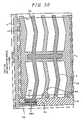
- the number of spacers 10 which are disposed at the center of the display regionis more than at any other portion of the display region.
- the density of the spacers forming near the sealing material 24is less than the density of the spacers forming at the center of the display region.
- the density of spacersis number of spacers per 1 cm.sup.2 or 1 mm.sup.2. So, the spacers which are disposed far from the sealing material 24 are required for the gap maintenance force in proportion to the size of the liquid crystal display panel.
- the thickness of a substrate for LCDis 0.7 mm or less, the large size LCD substrate bends easily by virtue of its weight. In this embodiment, many spacers 10 keep a gap between substrates, preventing bending in large size LCD panels.
- the spacer 10is formed like the twenty-second embodiment by the selective etching of a photo-lithography method. Moreover, the, density of the spacer from the center to the edge of the substrate should change smoothly, and not suddenly. If the density of the spacer changes suddenly, the gap between substrates would not be uniform. In this embodiment, it allows the density of the spacer to be different from the center portion in the direction and the Y direction. Hefice, the density of the spacer at the center portion in the X direction is more than in the Y direction to prevent A substrate from bending efficiently.
- FIG. 25is a plan view of the pixel of a liquid crystal display according to a twenty-third embodiment of the present invention.
- the spacers 10are arranged uniformly, but the width of the spacers 10 disposed at the center of a display region is wider than other spacers 10 in other region. Hence, a square measure where the spacers touch the substrates is different between the center region and the edge region.
- the spacer 10is formed like the twenty-second embodiment by a selective etching of a photo-lithography method. Moreover, it allows the material strength of spacers to be different between the center region and the edge region.
- the spacer 10is not only formed in the pixel whose color filter is green. Rather, the spacer 10 is formed selectively in the pixels whose color filters are red or blue. Because green is the highest light transmittance color among red, green and blue, an observer can recognize an improper image display in green pixel easily.
- FIG. 26is a plan view of the pixel of a liquid crystal display according to a twenty-fifth embodiment of the present invention.
- a portion 20functions as a shield material to hide alignment defects which are caused by the rubbing in the initial orientation direction.
- the portion 20combines the shield material and the counter electrode 4 A which is arranged at the side of the pixel. Therefore, the material of the counter electrode 4 A is selected from the group consisting of aluminum, chromium, a metal alloy including. aluminum or chromium as a main component, and so on.
- FIG. 27is a plan view of the pixel of a liquid crystal display according to a twenty-sixth embodiment of the present invention.
- a portion 20functions as a shield material to hide alignment defects which are caused by the rubbing in the initial orientation direction.
- the portion 20combines the shield material and the pixel electrode 5 . Therefore, the material of the pixel electrode 5 is selected from the group consisting of aluminum, chromium, a metal alloy including aluminum or chromium as a main component, and so on.
- FIG. 28is a plan view of the pixel of a liquid crystal display according to a twenty-seventh embodiment of the present invention.
- a portion 20functions as a shield material to hide alignment defects which are caused by the rubbing in the initial orientation direction.
- the portion 20combine the shield material and the counter electrode 4 A which is arranged at the center of the pixel. Therefore, the material of the counter electrode 4 A is selected from the group of aluminum, chromium, a metal alloy including aluminum or chromium as a main component, and so on.
- FIG. 29is a plan view of the pixel of a liquid crystal display according to a twenty-eighth embodiment of the present invention.
- a portion 20functions as a shield material to hide alignment defects which are caused by the rubbing in the initial orientation direction.
- the portion 20combines the shield material and the pixel electrode 5 . Therefore, the material of the pixel electrode 5 is selected from the group consisting of aluminum, chromium, a metal alloy including aluminum or chromium as a main component, and so on.
- the portion 20 of the pixel electrode 5is wider than another portion for increasing shield area and improving the precision of the design of a TFT cell.
- FIG. 30is a plan view of the pixel of a liquid crystal display according to a twenty-ninth embodiment of the present invention.
- a portion 20functions as a shield material to hide alignment defects which are caused by the rubbing in the initial orientation direction.
- the portion 20combines the shield material and the counter electrode 4 A which is arranged at the center or a pixel. Therefore, the material of the counter electrode 4 A is selected from the group of consisting of aluminum, chromium, a metal alloy including aluminum or chromium as a main component, and so on.
- the portion 20 of the counter electrode 4 Ais wider than another portion for increasing shield area and improving the precision of the design of a TFT cell.
- this inventionis to provide a multi-domain system IPS (In-Plane Switching mode) liquid crystal display which has high contrast and does not have an improper image display.
- IPSIn-Plane Switching mode
- this inventionachieves both advantages of preventing advantages the inversion of luminance when the view point of the observer is at an angle with respect to the slanting direction of the liquid crystal display panel, and providing remarkably high contrast (350:1) and high aperture ratio for a color active matrix liquid crystal display.
Landscapes
- Physics & Mathematics (AREA)
- Nonlinear Science (AREA)
- Chemical & Material Sciences (AREA)
- Crystallography & Structural Chemistry (AREA)
- General Physics & Mathematics (AREA)
- Optics & Photonics (AREA)
- Mathematical Physics (AREA)
- Engineering & Computer Science (AREA)
- Liquid Crystal (AREA)
- Manufacturing & Machinery (AREA)
- Geometry (AREA)
- Microelectronics & Electronic Packaging (AREA)
Abstract
Description
- This application is a Continuation of nonprovisional U.S. application Ser. No. 11/079,375 filed on Mar. 15, 2005, which is a Continuation of nonprovisional U.S. application Ser. No. 10/659,369 filed on Sep. 11, 2003, which is a Continuation of nonprovisional U.S. application Ser. No. 10/106,954 filed on Mar. 28, 2002. Priority is claimed based on U.S. application Ser. No. 11/079,375 filed on Mar. 15, 2005, which claims the priority of U.S. application Ser. No. 10/659,369 filed on Sep. 11, 2003, which claims the priority of U.S. application Ser. No. 10/106,954 filed on Mar. 28, 2002, which claims the priority of Japanese Application 11-029053 filed on Feb. 5, 1999, all of which is incorporated by reference.
- 1. Field of the Invention
- The present invention relates to a liquid crystal display device. More specifically, the invention relates to a liquid crystal display device with high contrast characteristics of the multi-domain system using spacers.
- 2. Description of the Prior Art
- Active matrix liquid crystal display devices using active elements as represented by thin-film transistors (TFT) have now been widely used as display terminals of OA equipment since they are light in weight and have picture quality equivalent to that of cathode-ray tubes.
- The display system of the liquid crystal display devices can be roughly divided into two. One is a system in which liquid crystals are sandwiched by two substrates having transparent electrodes and are driven by a voltage applied to the transparent electrodes, and light incident upon the liquid crystals and transmitted through the transparent electrodes is modulated to achieve display.
- Another one is a system in which liquid crystals are driven by an electric filed which is nearly in parallel with the surface of a substrate between two electrodes that are formed on the same substrate, and light incident upon the liquid crystals through a gap between the two electrodes is modulated to provide display.
- Features of the latter system have been disclosed in, for example, U.S. Pat. No. 5,576,867, U.S. Pat. No. 5,599,285, U.S. Pat. No. 5,598,285, U.S. Pat. No. 5,786,876, U.S. Pat. No. 5,956,111 and Japanese Patent No. 02907137. Moreover features of a multi-domain system IPS (In-Plane Switching mode) liquid crystal display have been disclosed in, for example, U.S. Pat. No. 5,745,207.
- In general, an orientation process that prepares an orientation film for controlling liquid crystal molecules is done by rubbing using a rotating rubbing roller on the surface of an orientation film. However, when spaces are formed on an orientation layer, an orientation process can cause alignment defects as a result of the differences in surface level. Specifically, when spacers are formed in the display region, alignment defect can result in an improper image display.
- Accordingly, an object of the present invention is to provide multi-domain system IPS (In-Plane Switching mode) liquid crystal display which have high contrast and do not suffer from improper image display. This invention provide a remarkable high contrast display (350:1) as compared to current model displays (200:1).
- According to one aspect of the present invention, there is provided a black matrix formed between a pair of substrates and formed over a plurality of drain lines and gate lines, a plurality of spacers arranged under the black matrix, wherein a plurality of liquid crystal molecules aligned to a boundary direction of the black matrix in the OFF state, and, having a first group and a second group in the ON state, wherein a switching angle of the second is opposite to a switching angle of the first group.
- According to another aspect of the present invention, there is provided a black matrix formed between a pair of substrates and formed over a plurality of drain lines and gate lines, a plurality of spacers arranged under the black matrix, wherein a plurality of liquid crystal molecules having Y direction of an initial orientation angle, and twisted to +X direction and −X direction when a driving voltage is applied.
- According to another aspect of the present invention, there is provided a plurality of liquid crystal molecules having a positive dielectric constant anisotropy and interposed between a pair of orientation layers, a black matrix formed over another of a pair of substrates in a matrix shape, a plurality of spacers formed between the black matrix and one of the pair of orientation layers, wherein a plurality of liquid crystal molecules having Y direction of an initial orientation angle, and twisted to +X direction and −X direction when a driving voltage is applied.
- According to another aspect of the present invention, there is provided a plurality of liquid crystal molecules having a negative dielectric constant anisotropy and interposed between said pair of orientation layers, a black matrix formed over another of a pair of substrates in a matrix shape, a plurality of spacers formed between the black matrix and one of a pair of orientation layers, wherein said plurality crystal molecules having X direction of an initial orientation angle, and twisted to +Y direction and −Y direction when driving voltage is applied.
FIG. 1 is a plan view of the pixel of a liquid crystal display according to a first embodiment of the present invention.FIG. 2 is a sectional view of the pixel of a liquid crystal display cut along the line II-II in1.FIG. 3 is a sectional view of the spacer in illustration of a alignment defect on an orientation layer.FIG. 4 is a plan view of the pixel of a liquid crystal display according to a second embodiment of the present invention.FIG. 5 is a plan view of the pixel of a liquid crystal display according to a third embodiment of the present invention.FIG. 6 is a plan view of the pixel of a liquid crystal display according to a fourth embodiment of the present invention.FIG. 7 is a plan view of the pixel of a liquid crystal display according to a fifth embodiment of the present invention.FIG. 8 is a sectional view of the liquid crystal display according to a seventh embodiment of the present invention.FIG. 9 is a sectional view of the liquid crystal display according to a eight embodiment of the present invention.FIG. 10 is a sectional view of the spacer of a liquid crystal display according to a tenth embodiment of the present invention.FIG. 11A is a plan view of the pixel of a liquid crystal display according to a ninth embodiment of the present invention.FIG. 11B is a plan view of the pixel of a liquid crystal display according to a tenth embodiment of the present invention.FIG. 12 is a sectional view of the spacer of a liquid crystal display according to an eleventh embodiment 11 of the present invention.FIG. 13 is a flow chart of a sectional view of A spacer illustrating the steps A to E of fabricating asubstrate 1B.FIG. 14 , is a flow chart of a sectional view of a, spacer illustrating the steps A to E of fabricating asubstrate 1B.FIG. 15 is a sectional view of the spacer of A liquid crystal display according to a fourteenth embodiment of the present invention.FIG. 16 is a sectional view of the spacer of a liquid crystal display according another invention of the fourteenth embodiment.FIG. 17 is a sectional view of the spacer of a liquid crystal display according to a fifteenth embodiment of the present invention.FIG. 18 is a plan view of the pixel of a liquid crystal display according to a sixteenth embodiment of the present invention.FIG. 19 is a plan view of the pixel of a liquid crystal display according to another invention of the sixteenth embodiment.FIG. 20 is a plan view of the pixel of a liquid crystal display according to a seventh embodiment of the present invention.FIG. 21 is a plan view of the pixel of a liquid crystal display according to an eighteenth embodiment of the present invention.FIG. 22 is a plan view of the pixel of a liquid crystal display according to a nineteenth embodiment of the present invention.FIG. 23 is a plan view of the pixel of a liquid crystal display according to a twenty-first embodiment of the present invention.FIG. 24 is a plan view of the pixel of a liquid crystal display according to a twenty-second embodiment of the present invention.FIG. 25 is a plan view of the pixel of a liquid crystal display according to a twenty-third embodiment of the present invention.FIG. 26 is a plan view of the pixel of a liquid crystal display according to a twenty-fifth embodiment of the present invention.FIG. 27 is a plan view of the pixel of a liquid crystal display according to a twenty-sixth embodiment of the present invention.FIG. 28 is a plan view of the pixel of a liquid crystal display according to a twenty-seventh embodiment of the present invention.FIG. 29 is a plan view of the pixel of a liquid crystal display according to a twenty-eighth embodiment of the present invention.FIG. 30 is a plan view of the pixel of a liquid crystal display according to a twenty-ninth embodiment of the present invention.- This present invention will hereunder be described in more detail.
FIG. 1 is a plan view of the pixel of a liquid crystal display according to a first embodiment of the present invention. In the first embodiment, a plurality of liquid crystal molecules having a positive dielectric constant anisotropy, andFIG. 1 shows one pixel of a plurality of pixels forming in matrix shape. Each pixel is defined in a region where twoadjacent gate lines 2 and twoadjacent drain lines 3 intersect. And each pixel includes a thin-film transistor TFT, a capacitor Cadd, apixel electrode 5, a counter electrode4A and acounter voltage line 4. The gate lines2 and thecounter voltage lines 4 extend in the X direction in the drawing and are arranged in the Y direction. Thedrain lines 3 extend in the Y direction and are arranged in the X direction. Thepixel electrode 5 is connected to the thin-film transistor TFT. The material of thegate line 2 is selected from a group of chromium, aluminum and molybdenum, and thecounter voltage line 4 is formed by the same material with thegate line 2.- A counter voltage is supplied to the counter electrodes4A via the
counter voltage line 4 from an external circuit. And the counter electrodes4A and thecounter voltage line 4 have a shape of a letter H in the each pixels. Thepixel electrode 5 and the counter electrode4A are opposed to each other, and the optical state of the liquid crystals LC (ON state) is controlled by an electric field between eachpixel electrode 5 and the counter electrode4A, thereby to control the display. Thepixel electrodes 5 and the counter electrodes4A are formed like comb teeth, and extend in a slender form in the Y direction. - Here, the
pixel electrode 5 and the counter electrode4A have a herringbone shape for the multi-domain system. The counter electrode4A maintains the distance with thepixel electrode 5 by increasing the width of the counter electrode4A. Hence, the face of thedrain line 3 side of the counter electrode4A is formed parallel with thedrain line 3, and the face of thepixel electrode 5 side of the counter electrode4A is formed parallel with thepixel electrode 5. - Therefore, the direction of the electric field which is disposed in the upper pixel region of the
counter voltage line 4 in a pixel between thepixel electrode 5 and the counter electrode4A is different from the lower one pixel region. InFIG. 1 , the direction of the electric field which is disposed at the upper pixel region has the angle of +.theta. with respect to the direction parallel to thecounter voltage line 4, but the direction of the electric field which is disposed at the lower one has the angle of −.theta. with respect to the direction parallel to thecounter voltage line 4. - The above-mentioned shape provides liquid crystal molecules to switch in reverse directions at each pixel region, and a light transmittance change at each pixel.
- In this invention, it can prevent the inversion of luminance when the view point of the observer is at an angle with respect to the slanting direction of the liquid crystal display panel. In the first embodiment, one pixel has the difference angle of .+−.theta. dividing upper and lower pixel region, but it allows two adjoining two pixels to have difference angles of +.theta. and −.theta., respectively.
- Thin film transistor TFT consists of the
gate line 2, a drain electrode3A, asource electrode 5A, asemiconductor layer 6 and a gate insulator (silicon nitride). An insulator is formed on thegate line 2 as a gate insulator, and thesemiconductor layer 6 whose material is amorphous silicon formed on the gate insulator. A drain electrode3A and asource electrode 5A are formed on thesemiconductor layer 6; thin film transistor TFT becomes an inverted stagger type thin film transistor. The drain electrode3A and asource electrode 5A are same layer, and the drain electrode3A contact with the drain line, and thesource electrode 5A contact with the pixel electrode, respectively. - In the first embodiment, an initial orientation angle is the Y direction, so a rubbing direction is also the Y direction. The absolute value of the angle between the
drain line 3 and the direction of the electric field E is larger than the absolute value of the angle between thecounter voltage line 4 and the direction of the electric field E. A capacitance Cadd consists of thepixel electrode 5, thecounter voltage line 4 and the gate insulator. To form the capacitance Cadd on thecounter voltage line 4, the capacitance Cadd can be larger than any region in a pixel. The capacitance Cadd functions to improve the data retentivity. A protective film PAS (silicon nitride) is formed over thetransparent substrate 1A after forming a plurality of thin film transistors TFT and pixels for preventing to touch with liquid, crystal molecules. Furthermore, an orientation layer which controls an initial orientation angle of liquid crystal molecules is formed over the protective film PAS. The orientation layer is surface rubbed with a rubbing roller along with the Y direction after coating synthetic resins thereon. - A
color filter substrate 1B consists of a black matrix BM, acolor filter 7 and anorientation layer 9. InFIG. 1 , a boundary of the black matrix BM is shown as a plan view, and inFIG. 2 . shows a sectional view of the black matrix BM. Here, theorientation layer 9 of thecolor filter substrate 1B is a surface rubbed with rubbing roller in the Y direction after coating synthetic resins thereon the same as the orientation layer of thetransparent substrate 1A. Also, the orientation direction of each orientation layer of thetransparent substrate 1A side and that of thecolor filter substrate 1B are the same Y direction. Therefore, a plurality of liquid crystal molecules are aligned to a boundary direction of the black matrix in the OFF state, and having the upper pixel region (a first group) and the lower pixel region (a second group) in the ON state, wherein a switching angle of the second group is opposite to a switching angle of the first group. - A
spacer 10 is formed between thetransparent substrate 1A and thecolor filter substrate 1B and formed over thedrain line 3 to keep a gap therebetween. FIG. 2 is a sectional view of the pixel of a liquid crystal display cut along the line II-II inFIG. 1 . The black matrix BM is formed on thecolor filter substrate 1B which faces with liquid crystal molecules, thespacer 10 is made of the black matrix BM, thespacers 10 function to keep a gap between thetransparent substrate 1A side and thecolor filter substrate 1B.- The black matrix BM is formed by the twice selective etching of a photo lithography method, the first selective etching to make the
spacer 10 after coating black matrix material very thick, and the second selective etching to make a hole for thecolor filter 7. The black matrix BM is formed with either thedrain line 3 or thegate line 2 thereon; a light transmittance region between thepixel electrode 5 and the counter electrode4A are formed in an open region of the black matrix BM. An end of thepixel electrode 5 and the edge of the counter electrode4A are covered with the black matrix BM, because this region is not the uniform electric field area between thepixel electrode 5 and the counter electrode4A. - The open region of the black matrix BM would be able to improve an aperture ratio if it is large enough. On the other hand, the open region of the black matrix should be designed to cover the unnecessary electric field between the
drain line 3 and the counter electrode4A, and the improper electric field between thepixel electrode 5 and the edge of counter electrode4A. Thecolor filter 7 is formed at the open region of the black matrix BM. Then, the overcoating film 8 is formed over thecolor filter 7. Finally, theorientation layer 9 is formed over the overcoating film 8. FIG. 3 is a sectional view of thespacer 10 in illustration of an alignment defect on an orientation layer. Theorientation layer 9 has its surface rubbed with rubbingroller 100 in the right direction (in the Y direction inFIG. 1 ). Here, anarea 200 is not orientated and causes an alignment defect with thespacer 10. Hence, in thearea 200, the rubbingroller 100 out of contact with surface of theorientation layer 9, is not rubbed with the rubbingroller 100. Therefore, in this invention, thearea 200 brings in the Y direction by using the multi-domain system IPS, and covers thearea 200 by the black matrix. As a result, this combination provides remarkably high contrast (350:1) for a liquid crystal display.- Moreover, the
spacer 10 is available to form over thecounter voltage line 4 as other embodiment. As the counter voltage. As thecounter voltage line 4 can be designed wider than thegate line 2, thedrain line 3 and another electrode, thearea 200 can be covered by thecounter voltage line 4 easily. FIG. 4 is a plan view of the pixel of a liquid crystal display according to a second embodiment of the present invention. In the second embodiment, a plurality of liquid crystal molecules having a negative dielectric constant anisotropy, rubbing direction (initial orientation angle) is in the X direction, so thespacer 10 is disposed over thegate line 2. As a result, even if alignment defects are formed thearea 200 on thegate line 2, thearea 200 is hid by the black matrix BM. A plurality of liquid crystal molecules have the X direction for an initial orientation angle, and are twisted to +Y direction and −Y direction while a driving voltage is applied.FIG. 5 is a plan view of the pixel of a liquid crystal display according a third embodiment of the present invention. In the embodiment, a plurality of liquid crystal molecules having a positive dielectric constant anisotropy, thepixel electrodes 5 and the counter electrodes4A are formed in the direction X which are parallel with thegate line 2. In the third embodiment, an rubbing direction (initial orientation angle) is in the X direction.- In
FIG. 5 , the direction of the electric field which is disposed at the upper pixel region has the angle of −.theta. with respect to the direction perpendicular to thecounter voltage line 4, but the direction of the electric field which is disposed at the lower pixel region has the angle of +.theta. with respect to the direction perpendicular to thecounter voltage fine 4. The above-mentioned shape provides the liquid crystal molecules with the ability to switch in reverse directions at each pixel region, and a light transmittance change in a pixel. - As each counter electrode4A is arranged parallel with each
pixel electrode 5, each of the counter electrodes4A has a wider portion than thepixel electrodes 5. The absolute value of the angle between thedrain line 3 and the direction of the electric field E is smaller than the absolute value of the angle between thegate line 2 and the direction of the electric field E. In this embodiment, an observer does not recognize the inversion of luminance when the view point of the observer is at an angle with respect to the slanting direction of the liquid crystal display panel. - A rubbing direction (initial orientation angle) of the
transparent substrate 1A and thecolor filter substrate 1B are in the same X direction as the direction ofgate line 2, so thespacer 10 is disposed over thegate line 2. As a result, even if alignment defects are made in thearea 200 on thegate line 2, thearea 200 is hidden by the black matrix BM in this embodiment. - This embodiment achieves both advantages of preventing the inversion of luminance when the view point of the observer is at an angle with respect to the slanting direction of the liquid crystal display panel, and of providing remarkably high contrast (350:1) for the liquid crystal display.
FIG. 6 is a plan view of the pixel of a liquid crystal display according to a fourth embodiment of the present invention. In the fourth embodiment, a plurality of liquid crystal molecules having a negative dielectric constant anisotropy, a rubbing direction (initial orientation angle) is in the Y direction. Thespacer 10 is disposed over thedrain line 3. As a result, even if alignment defects are made in thearea 200 on thedrain line 3, thearea 200 is hidden by the black matrix BM this embodiment.- That is, it can prevent the inversion of luminance when the view point of the observer is at an angle with respect to the slanting direction of the liquid crystal display panel.
- This embodiment achieves the of advantages both of preventing the inversion of luminance when the view point of the observer is at an angle with respect to the slanting direction of the liquid crystal display panel, and of providing remarkably high contrast (350:1) for the liquid crystal display.
FIG. 7 is a plan view of the pixel of a liquid crystal display according to a fifth embodiment of the present invention.FIG. 7A shows a plan view of an arrangement of a plurality of pixel. An black frames shows the black matrix BM, it's open region corresponds to each pixel. The arrangement inFIG. 7A is called the delta arrangement, one group of pixels in the X direction (a row direction) is offset to the side by ½ pitch relative to another group of pixels. As the delta arrangement, with pixels of red, green and blue adjacent each other, is useful for a color active matrix liquid crystal display. In thefifth embodiment 5, thespacer 10 is formed over thegate line 2, and, the rubbing direction (initial orientation angle) is in the X direction. As a result, even if alignment defects are made the are made in thearea 200 on thegate line 2, thearea 200 is hidden by the black matrix BM.FIG. 7B shows a plan view of the delta arrangement, when thespacer 10 is formed over thedrain line 3 and the rubbing direction (initial orientation angle) is in the Y direction. In this case, alignment defects inside the pixel region, cause an improper image display.- The delta arrangement may be designed such that one group pixels of the Y direction (a column direction) is offset to one side by ½ pitch relative to another group of pixels. In a sixth embodiment, the
spacer 10 is formed over thedrain line 3, the rubbing direction (initial orientation angle) is in the direction along with thedrain line 3. FIG. 8 is a sectional view of the liquid crystal display according to a seventh embodiment of the present invention.FIG. 8 shows a sectional view of thespacer 10 of a liquid crystal display cut along thegate line 2 inFIG. 1 . Thespacer 10 consists of the spacer10A which is formed at both ends of thegate line 2. (FIELD A), and the spacer10B which is formed at a pixel region (FIELD B). A sealingmember 24 seals between thetransparent substrate 1A and thecolor filter substrate 1B. Furthermore, aconductive layer 21 is formed under the spacer10A and10B forming on thecolor filter substrate 1B side, which is contacted with thegate line 2. Hence, this embodiment covers the spacer10A with theconductive layer 21 and electrically contracts thegate line 2 with the spacer10A. If thegate line 2 breakdown in its wiring at a part in FIELD B, scanning signals would be supported via theconductive layer 21 at FIELD A. The seventh embodiment is useful for video signals of thedrain line 3 as another embodiment.FIG. 9 is a sectional view of the liquid crystal display according to an eight embodiment of the present invention.FIG. 9 shows a sectional view of thespacer 10 of a liquid crystal display cut along thecounter voltage line 4 inFIG. 1 . Thespacer 10 consists of the spacer10A which is formed at both ends of the gate line2 (FIELD A), and the spacer10B which is formed at a pixel region (FIELD B). A sealingmember 24 seals between thetransparent substrate 1A and thecolor filter substrate 1B. Furthermore, anothercounter voltage line 22 is formed under the spacer10A and10B forming on thecolor filter substrate 1B side in this embodiment. Aconductive layer 23 is disposed likeFIG. 9 , and connects between thecounter voltage line 22 and an external terminal for a counter, voltage. Hence, this embodiment covers the spacer10A with thecounter voltage line 22, and electrically contacts theconductive layer 23 for a counter voltage.- It is clear that the
spacer 10 should be formed on the color filter substrate side to prevent any deterioration in the characteristics of a thin film transistor. In the process of the spacer forming on the same substrate with a film transistor, a step increasing for a selective etching by a photo lithography method is added, wherein the etching solvent causes deterioration of the characteristics of the thin film transistor. - However, the
spacer 10 should be formed on thetransparent substrate 1A side, when the alignment between the transparent substrate,1A, and thecolor filter substrate 1B is more important than the deterioration in the characteristics of a thin film transistor. FIG. 10 is a sectional view of the spacer of a liquid crystal display according to a tenth embodiment of the present invention. The black matrix BM and thecolor filter 7 are formed under thecolor filter substrate 1B side which is opposite to the liquid crystal, anovercoating film 8 made from a thermosetting resin film is in formed thereunder. The spacer made from a photocurable resin film, is formed under the overcoating film 8. To make thespacer 10 from photo curable resin film, a selective etching method is excluded from the process of thespacer 10, manufacturing steps for thecolor filter substrate 1B become simple and low cost. Theembodiment 10 is useful for, thetransparent substrate 1A side having thespacer 10 as another embodiment.FIG. 11A is a plan view of the pixel of a liquid crystal display according to an eleventh embodiment of the present invention. The spacers are uniformly arranged in a plurality of pixels like the same number of pixels have the same number of the spacers. To decrease alignment defects caused by spacer, a plurality of pixels have one spacer uniformly.FIG. 11B is a plan view of the pixel of a liquid crystal display according to a twelfth embodiment of the present invention. A plurality of pixels are dotted with a plurality of spacers. Thus, the spacers are not uniformly arranged in a plurality of pixels likeFIG. 11A . If alignment defects is uniform, an observer could see them easily.FIG. 12 is a sectional view of the spacer of a liquid crystal display according to a thirteenth embodiment of the present invention. Thespacer 10 adheres to an orientation layer formed on thetransparent substrate 1A by an adhesive30. The portion where thespacer 10 adheres to an orientation layer is touched between orientation layers. In general, the bonding force between the orientation layers having the same material is weak. Consequently, the adhesive30 including the Si coupling material is needed between orientation layers.FIG. 13 is a flow chart of sectional views of a spacer illustrating the steps A to E of fabricating acolor filter substrate 1B.- [Step 1]
FIG. 13A shows acolor filter substrate 1B having thespacer 10 coating an orientation material.- [Step 2]
- First, the
color filter substrate 1B is moved near a vessel filled withadhesive material 30 likeFIG. 13B . Then, thecolor filter substrate 1B is positioned to apply the top of thespacer 10 with adhesive material. - [Step 3]
FIG. 13C . shows, thespacer 10 having the adhesive30.- [Step 4]
- Second, the
transparent substrate 1A and-thecolor filter substrate 1B are positioned facing each other shown inFIG. 13D . - [Step 5]
- Finally, by applying heat to the pair of substrates, the adhesive30 begins going solidify (
FIG. 13E ). FIG. 14A is a flow chart of sectional views of a spacer illustrating the steps A to E of fabricating asubstrate 1B according to another embodiment.- [Step 1]
FIG. 14A shows acolor filter substrate 1B having thespacer 10 formed on an orientation material.- [Step 2]
- First, the
color filter substrate 1B is coated by theroller 31 soaking in the a vessel filled with adhesive material shown inFIG. 14B . As a result, thecolor filter substrate 1B is formed with the tops of thespacer 10 covered with adhesive material. - [Step 3]
FIG. 14C shows thespacer 10 having the adhesive30.- [Step 4]
- Second, the,
transparent substrate 1A, and thecolor filter substrate 1B are positioned facing each other shown inFIG. 14D . - [Step 5]
- Finally, by applying heat to the pair of substrates, then the adhesive30 begins to solidify (
FIG. 14E ). FIG. 15 is a sectional view of the spacer of a liquid crystal display according to a fourteenth embodiment of the present invention A concave40 is formed on thetransparent substrate 1A as a counter tapered shape of a protective film41 whereby adheres thespacer 10 with the protective film41 via the concave40. In the embodiment, the concave40 is used instead of the adhesive30.FIG. 16 is a sectional view of the spacer of a liquid crystal display according to another invention of the fourteenth embodiment. A concave42 is formed on thetransparent substrate 1A with thegate line 2 or thedrain line 3, wherein the concave42 fits with thespacer 10. In this embodiment, the concave42 is used instead of the adhesive30 or the concave40 Moreover, an area between theconcaves 42 may be formed larger than the width of thespacer 10, as the sealingmaterial 24 holds a gap of substrates correspond to the perpendicular direction. Therefore, theconcaves 42 function as holding material for a gap of substrates correspond to the parallel direction.FIG. 17 is a sectional view of the spacer of a liquid crystal display according to a fifteenth embodiment of the present invention. Thespacer 10 is formed over the drain overline 3, the black matrix BM's pattern adjacent to thespacer 10 is formed wider than the other portions. In the embodiment 15, a rubbing direction of the orientation layer follows with thedrain line 3. When an alignment defect is so large that the black matrix BM can not hide it perfectly, the embodiment 15 is useful thereby.FIG. 18 is a plan view of the pixel of a liquid crystal display according to a sixteenth embodiment of the present invention. In this embodiment, a rubbing direction of an orientation layer has an angle .theta., whereby alignment defects of the orientation layer caused by thespacer 10 also appear at an angle .theta. As alignment defects of the orientation layer are related to the rubbing direction, therefore the right black matrix BM's pattern is wider than the left black matrix BM's pattern.- In other words, the black matrix BM's pattern covering the
spacer 10 is needed as an outline whose shape is a circle with the center of the spacer, the radius of the circle depending on the occurrence of alignment defects. FIG. 19 is a plan view of the pixel of a liquid crystal display according another invention of the sixteenth embodiment. It allows the black matrix BM's pattern covering thespacer 10 to form at one side.FIG. 20 is a plan view of the pixel of a liquid crystal display according to a seventeenth embodiment of the present invention. Thespacer 10 is formed 6ver thegate line 2 or thedrain line 3. Ashield layer 50 is disposed adjacently both sides of thespacer 10. In this embodiment, theshield layer 50 is different layer from the black matrix BM, thegate line 2 and thedrain line 3. The rubbing direction of the orientation layer is the direction along with thegate line 2 or thedrain line 3. As alignment defects the orientation layer are related to the rubbing direction, theshield layer 50 is arranged wider than the field occurring alignment defects. Moreover, it allows theshield layer 50 to form the same layer with thegate line 2 or thedrain line 3, so as to be united with thegate line 2 or thedrain line 3. When theshield layer 50 is different layer from thedrain line 3, theshield layer 50 is made of the same material of thecounter voltage line 4. When theshield layer 50 is different layer from thegate line 2, theshield layer 50 is made of the same material of thedrain line 3. In another embodiment, it allows a rubbing direction of an orientation layer to have an angle .theta., wherein theshield layer 50 is formed wider than the field occurring alignment defect.FIG. 21 is a plan view of the pixel of a liquid crystal display according to an eighteenth embodiment of the present invention. Thespacer 10 is formed over thegate line 2 or thedrain line 3, and ashield layer 50 is disposed at the one side of thespacer 10. In more detail, theshield layer 50 is only formed on the side occurring alignment defect. In this way, an aperture ratio of a pixel can be improved more than embodiment 17.FIG. 22 is a plan view of the pixel of a liquid crystal display according to a nineteenth embodiment of the present invention. Theshield layer 50 is disposed adjacent both sides to thespacer 10. In this embodiment, the right side of theshield layer 50 is longer in the Y direction than the left side.- As alignment defects of the orientation layer are related to the rubbing direction, the
shield layer 50 is longer in the right than in the left. In other words, theshield layer 50 is needed as an outline whose shape is a circle with the center of the spacer, the radius of the circle depending on the occurrence of alignment defect. FIG. 23 is a plan view of the pixel of a liquid crystal display according to a twenty-first embodiment of the present invention. In the embodiment. 17-20, theshield layer 50 only functions as light shielding material, but this embodiment makes use of theshield layer 50 as any electrodes. InFIG. 23 , the counter electrodes4A which is disposed on the both sides of thedrain line 2 have the function as theshield layer 50. If the width of the counter electrodes4A is formed enough to hide alignment defects perfectly, the initial orientation angle would be designed not to depend on the presence of alignment defects. The reliability of the design improves by this embodiment.FIG. 24A is a plan view of the pixel of a liquid crystal display according to a twenty-second embodiment of the present invention.FIG. 24B is a sectional view of the pixel of a liquid crystal display cut along the line b.-b inFIG. 24A . A pair of thetransparent substrate 1A and thecolor filter substrate 1B face each other, the sealingmaterial 24 is formed between the substrates as a frame to keep a gap between the substrates thereby. Thespacer 10 is arranged inside the sealingmaterial 24 to keep a gap at the display region thereby. Thespacer 10 is formed on of a pair of the substrates, every spacer having the same square measurement where the spacer touches the other of the pair of substrates.- In addition, the number of
spacers 10 which are disposed at the center of the display region is more than at any other portion of the display region. Thus, the density of the spacers forming near the sealingmaterial 24 is less than the density of the spacers forming at the center of the display region. By definition, the density of spacers is number of spacers per 1 cm.sup.2 or 1 mm.sup.2. So, the spacers which are disposed far from the sealingmaterial 24 are required for the gap maintenance force in proportion to the size of the liquid crystal display panel. In general, the thickness of a substrate for LCD is 0.7 mm or less, the large size LCD substrate bends easily by virtue of its weight. In this embodiment,many spacers 10 keep a gap between substrates, preventing bending in large size LCD panels. - The
spacer 10 is formed like the twenty-second embodiment by the selective etching of a photo-lithography method. Moreover, the, density of the spacer from the center to the edge of the substrate should change smoothly, and not suddenly. If the density of the spacer changes suddenly, the gap between substrates would not be uniform. In this embodiment, it allows the density of the spacer to be different from the center portion in the direction and the Y direction. Hefice, the density of the spacer at the center portion in the X direction is more than in the Y direction to prevent A substrate from bending efficiently. FIG. 25 is a plan view of the pixel of a liquid crystal display according to a twenty-third embodiment of the present invention. Thespacers 10 are arranged uniformly, but the width of thespacers 10 disposed at the center of a display region is wider thanother spacers 10 in other region. Hence, a square measure where the spacers touch the substrates is different between the center region and the edge region. Thespacer 10 is formed like the twenty-second embodiment by a selective etching of a photo-lithography method. Moreover, it allows the material strength of spacers to be different between the center region and the edge region.- In a twenty-fourth embodiment, the
spacer 10 is not only formed in the pixel whose color filter is green. Rather, thespacer 10 is formed selectively in the pixels whose color filters are red or blue. Because green is the highest light transmittance color among red, green and blue, an observer can recognize an improper image display in green pixel easily. FIG. 26 is a plan view of the pixel of a liquid crystal display according to a twenty-fifth embodiment of the present invention. In this embodiment, aportion 20 functions as a shield material to hide alignment defects which are caused by the rubbing in the initial orientation direction. Moreover, in this embodiment, theportion 20 combines the shield material and the counter electrode4A which is arranged at the side of the pixel. Therefore, the material of the counter electrode4A is selected from the group consisting of aluminum, chromium, a metal alloy including. aluminum or chromium as a main component, and so on.FIG. 27 is a plan view of the pixel of a liquid crystal display according to a twenty-sixth embodiment of the present invention. In this embodiment, aportion 20 functions as a shield material to hide alignment defects which are caused by the rubbing in the initial orientation direction. Moreover, in this embodiment, theportion 20 combines the shield material and thepixel electrode 5. Therefore, the material of thepixel electrode 5 is selected from the group consisting of aluminum, chromium, a metal alloy including aluminum or chromium as a main component, and so on.FIG. 28 is a plan view of the pixel of a liquid crystal display according to a twenty-seventh embodiment of the present invention. In this embodiment, aportion 20 functions as a shield material to hide alignment defects which are caused by the rubbing in the initial orientation direction. Moreover, in this embodiment, theportion 20 combine the shield material and the counter electrode4A which is arranged at the center of the pixel. Therefore, the material of the counter electrode4A is selected from the group of aluminum, chromium, a metal alloy including aluminum or chromium as a main component, and so on.FIG. 29 is a plan view of the pixel of a liquid crystal display according to a twenty-eighth embodiment of the present invention. In this embodiment, aportion 20 functions as a shield material to hide alignment defects which are caused by the rubbing in the initial orientation direction. Moreover, in this embodiment, theportion 20 combines the shield material and thepixel electrode 5. Therefore, the material of thepixel electrode 5 is selected from the group consisting of aluminum, chromium, a metal alloy including aluminum or chromium as a main component, and so on. Furthermore, theportion 20 of thepixel electrode 5 is wider than another portion for increasing shield area and improving the precision of the design of a TFT cell.FIG. 30 is a plan view of the pixel of a liquid crystal display according to a twenty-ninth embodiment of the present invention. In this embodiment, aportion 20 functions as a shield material to hide alignment defects which are caused by the rubbing in the initial orientation direction. Moreover, in this embodiment, theportion 20 combines the shield material and the counter electrode4A which is arranged at the center or a pixel. Therefore, the material of the counter electrode4A is selected from the group of consisting of aluminum, chromium, a metal alloy including aluminum or chromium as a main component, and so on. Furthermore, theportion 20 of the counter electrode4A is wider than another portion for increasing shield area and improving the precision of the design of a TFT cell. In this way, this invention is to provide a multi-domain system IPS (In-Plane Switching mode) liquid crystal display which has high contrast and does not have an improper image display. Thus, this invention achieves both advantages of preventing advantages the inversion of luminance when the view point of the observer is at an angle with respect to the slanting direction of the liquid crystal display panel, and providing remarkably high contrast (350:1) and high aperture ratio for a color active matrix liquid crystal display.
Claims (1)
Priority Applications (2)
| Application Number | Priority Date | Filing Date | Title |
|---|---|---|---|
| US11/797,319US7453541B2 (en) | 1999-02-05 | 2007-05-02 | Liquid crystal display having particular electrodes and a spacer |
| US12/285,732US20090122249A1 (en) | 1999-02-05 | 2008-10-14 | Liquid crystal display having particular electrodes and a spacer |
Applications Claiming Priority (6)
| Application Number | Priority Date | Filing Date | Title |
|---|---|---|---|
| JP11-029053 | 1999-02-05 | ||
| JP02905399AJP4094759B2 (en) | 1999-02-05 | 1999-02-05 | Liquid crystal display |
| US10/106,954US6667790B2 (en) | 1999-02-05 | 2002-03-28 | Liquid crystal display having particular spacer |
| US10/659,369US7030953B2 (en) | 1999-02-05 | 2003-09-11 | Liquid crystal display with gate lines and an edge of the black matrix elongated parallel to an initial orientation direction |
| US11/079,375US7248325B2 (en) | 1999-02-05 | 2005-03-15 | Liquid crystal display having particular electrodes and particular common line |
| US11/797,319US7453541B2 (en) | 1999-02-05 | 2007-05-02 | Liquid crystal display having particular electrodes and a spacer |
Related Parent Applications (1)
| Application Number | Title | Priority Date | Filing Date |
|---|---|---|---|
| US11/079,375ContinuationUS7248325B2 (en) | 1999-02-05 | 2005-03-15 | Liquid crystal display having particular electrodes and particular common line |
Related Child Applications (1)
| Application Number | Title | Priority Date | Filing Date |
|---|---|---|---|
| US12/285,732ContinuationUS20090122249A1 (en) | 1999-02-05 | 2008-10-14 | Liquid crystal display having particular electrodes and a spacer |
Publications (2)
| Publication Number | Publication Date |
|---|---|
| US20070206145A1true US20070206145A1 (en) | 2007-09-06 |
| US7453541B2 US7453541B2 (en) | 2008-11-18 |
Family
ID=12265645
Family Applications (6)
| Application Number | Title | Priority Date | Filing Date |
|---|---|---|---|
| US10/107,205Expired - LifetimeUS6552770B2 (en) | 1999-02-05 | 2002-03-28 | Liquid crystal display having shield layers on both sides of spacer across signal line |
| US10/106,954Expired - LifetimeUS6667790B2 (en) | 1999-02-05 | 2002-03-28 | Liquid crystal display having particular spacer |
| US10/659,369Expired - LifetimeUS7030953B2 (en) | 1999-02-05 | 2003-09-11 | Liquid crystal display with gate lines and an edge of the black matrix elongated parallel to an initial orientation direction |
| US11/079,375Expired - Fee RelatedUS7248325B2 (en) | 1999-02-05 | 2005-03-15 | Liquid crystal display having particular electrodes and particular common line |
| US11/797,319Expired - Fee RelatedUS7453541B2 (en) | 1999-02-05 | 2007-05-02 | Liquid crystal display having particular electrodes and a spacer |
| US12/285,732AbandonedUS20090122249A1 (en) | 1999-02-05 | 2008-10-14 | Liquid crystal display having particular electrodes and a spacer |
Family Applications Before (4)
| Application Number | Title | Priority Date | Filing Date |
|---|---|---|---|
| US10/107,205Expired - LifetimeUS6552770B2 (en) | 1999-02-05 | 2002-03-28 | Liquid crystal display having shield layers on both sides of spacer across signal line |
| US10/106,954Expired - LifetimeUS6667790B2 (en) | 1999-02-05 | 2002-03-28 | Liquid crystal display having particular spacer |
| US10/659,369Expired - LifetimeUS7030953B2 (en) | 1999-02-05 | 2003-09-11 | Liquid crystal display with gate lines and an edge of the black matrix elongated parallel to an initial orientation direction |
| US11/079,375Expired - Fee RelatedUS7248325B2 (en) | 1999-02-05 | 2005-03-15 | Liquid crystal display having particular electrodes and particular common line |
Family Applications After (1)
| Application Number | Title | Priority Date | Filing Date |
|---|---|---|---|
| US12/285,732AbandonedUS20090122249A1 (en) | 1999-02-05 | 2008-10-14 | Liquid crystal display having particular electrodes and a spacer |
Country Status (4)
| Country | Link |
|---|---|
| US (6) | US6552770B2 (en) |
| JP (1) | JP4094759B2 (en) |
| KR (1) | KR100708617B1 (en) |
| TW (1) | TW578025B (en) |
Families Citing this family (77)
| Publication number | Priority date | Publication date | Assignee | Title |
|---|---|---|---|---|
| JP3881124B2 (en)* | 1999-02-05 | 2007-02-14 | 株式会社日立製作所 | Liquid crystal display |
| JP2001084100A (en)* | 1999-08-27 | 2001-03-30 | Internatl Business Mach Corp <Ibm> | Touch sensor type liquid crystal display device and liquid crystal display device |
| JP2001305557A (en)* | 2000-04-21 | 2001-10-31 | Nec Corp | Liquid crystal display device |
| JP4446577B2 (en)* | 2000-09-06 | 2010-04-07 | エーユー オプトロニクス コーポレイション | Display panel, display device |
| JP2002131767A (en)* | 2000-10-27 | 2002-05-09 | Hitachi Ltd | Liquid crystal display |
| JP3680730B2 (en)* | 2000-12-08 | 2005-08-10 | 株式会社日立製作所 | Liquid crystal display |
| JP4884586B2 (en) | 2000-12-18 | 2012-02-29 | 株式会社 日立ディスプレイズ | Liquid crystal display |
| JP2002214621A (en)* | 2001-01-17 | 2002-07-31 | Toshiba Corp | Liquid crystal display |
| KR100748442B1 (en)* | 2001-02-26 | 2007-08-10 | 엘지.필립스 엘시디 주식회사 | Array board for horizontal electric field drive type liquid crystal display device and manufacturing method thereof |
| KR100658072B1 (en)* | 2001-04-18 | 2006-12-15 | 비오이 하이디스 테크놀로지 주식회사 | Fringe Field Drive LCD |
| KR100658073B1 (en)* | 2001-05-07 | 2006-12-15 | 비오이 하이디스 테크놀로지 주식회사 | LCD Display |
| EP1417671A2 (en)* | 2001-06-08 | 2004-05-12 | Thomson Licensing S.A. | Lcos column merory effect reduction |
| JP4305811B2 (en) | 2001-10-15 | 2009-07-29 | 株式会社日立製作所 | Liquid crystal display device, image display device and manufacturing method thereof |
| JP3782015B2 (en)* | 2002-01-22 | 2006-06-07 | 株式会社日立製作所 | Liquid crystal display |
| JP4057816B2 (en)* | 2002-01-31 | 2008-03-05 | 東芝松下ディスプレイテクノロジー株式会社 | Liquid crystal display |
| TWI243271B (en)* | 2002-05-17 | 2005-11-11 | Advanced Display Kk | Liquid crystal display device |
| JP4082493B2 (en)* | 2002-06-06 | 2008-04-30 | 株式会社 日立ディスプレイズ | Liquid crystal display |
| JP4090799B2 (en)* | 2002-07-01 | 2008-05-28 | 奇美電子股▲ふん▼有限公司 | Image display element and image display device |
| KR100878239B1 (en)* | 2002-09-06 | 2009-01-13 | 삼성전자주식회사 | Liquid Crystal Display and Thin Film Transistor Substrate |
| KR100920344B1 (en) | 2002-12-03 | 2009-10-07 | 삼성전자주식회사 | Thin film transistor array panel for liquid crystal display |
| KR100924227B1 (en)* | 2002-12-06 | 2009-11-02 | 엘지디스플레이 주식회사 | LCD panel and manufacturing method |
| KR100907479B1 (en)* | 2002-12-31 | 2009-07-13 | 삼성전자주식회사 | Color filter substrate and liquid crystal display having the same |
| TWI274946B (en)* | 2003-01-10 | 2007-03-01 | Toshiba Matsushita Display Tec | Liquid crystal display apparatus and method of manufacturing the same |
| TWI246618B (en)* | 2003-01-10 | 2006-01-01 | Toshiba Matsushita Display Tec | Liquid crystal display apparatus |
| JP2004252309A (en)* | 2003-02-21 | 2004-09-09 | Seiko Epson Corp | Electro-optical panel and electronic equipment |
| KR100959367B1 (en)* | 2003-10-13 | 2010-05-25 | 엘지디스플레이 주식회사 | Transverse electric field type liquid crystal display device |
| KR100961960B1 (en)* | 2003-11-18 | 2010-06-08 | 삼성전자주식회사 | Liquid crystal display device, thin film diode display panel and manufacturing method thereof |
| KR100672215B1 (en)* | 2003-12-15 | 2007-01-22 | 엘지.필립스 엘시디 주식회사 | Transverse electric field type liquid crystal display device and manufacturing method thereof |
| JP4516348B2 (en)* | 2004-04-21 | 2010-08-04 | 株式会社 日立ディスプレイズ | Liquid crystal display |
| TWI271574B (en)* | 2004-04-30 | 2007-01-21 | Innolux Display Corp | Liquid crystal display panel |
| KR101003829B1 (en)* | 2004-04-30 | 2010-12-23 | 엘지디스플레이 주식회사 | CIO structure liquid crystal display device and manufacturing method thereof |
| JP4155227B2 (en)* | 2004-05-07 | 2008-09-24 | セイコーエプソン株式会社 | Liquid crystal display device and electronic device |
| KR100675635B1 (en)* | 2004-05-10 | 2007-02-02 | 엘지.필립스 엘시디 주식회사 | Transverse field mode liquid crystal display with improved contrast ratio |
| KR101050348B1 (en)* | 2004-05-31 | 2011-07-19 | 엘지디스플레이 주식회사 | Transverse electric field liquid crystal display device |
| JP2005345584A (en)* | 2004-06-01 | 2005-12-15 | Casio Comput Co Ltd | Liquid crystal display |
| KR101026807B1 (en)* | 2004-06-09 | 2011-04-04 | 삼성전자주식회사 | Drive device and display panel for display device |
| US7433004B2 (en)* | 2004-06-11 | 2008-10-07 | Sharp Kabushiki Kaisha | Color filter substrate, method of making the color filter substrate and display device including the color filter substrate |
| KR101117978B1 (en)* | 2004-06-28 | 2012-03-06 | 엘지디스플레이 주식회사 | Liquid Crystal Display Device |
| US7949666B2 (en)* | 2004-07-09 | 2011-05-24 | Ricoh, Ltd. | Synchronizing distributed work through document logs |
| JP2006126788A (en)* | 2004-09-29 | 2006-05-18 | Seiko Epson Corp | Liquid crystal device and electronic device |
| CN100365493C (en)* | 2004-11-03 | 2008-01-30 | 中华映管股份有限公司 | Liquid crystal panel and method for manufacturing same |
| KR100682359B1 (en)* | 2004-11-16 | 2007-02-15 | 엘지.필립스 엘시디 주식회사 | Flat panel and its manufacturing method |
| KR100685955B1 (en)* | 2004-12-30 | 2007-02-23 | 엘지.필립스 엘시디 주식회사 | Liquid crystal display |
| JP2006330470A (en) | 2005-05-27 | 2006-12-07 | Sharp Corp | Liquid crystal display device and manufacturing method thereof |
| JP3974141B2 (en)* | 2005-06-23 | 2007-09-12 | 三菱電機株式会社 | Transflective liquid crystal display device |
| JP2007148372A (en)* | 2005-10-26 | 2007-06-14 | Hitachi Chem Co Ltd | Color filter for liquid crystal display device, photosensitive resin composition for liquid crystal spacer, and photosensitive element for liquid crystal spacer |
| CN100476525C (en)* | 2005-10-27 | 2009-04-08 | 中华映管股份有限公司 | Liquid crystal display panel and method for manufacturing the same |
| US7330235B2 (en)* | 2005-11-08 | 2008-02-12 | Chunghwa Picture Tubes, Ltd. | Liquid crystal display panel having spacers wedged in three-layered conductive lines and manufacturing method thereof |
| JP4884820B2 (en)* | 2006-04-12 | 2012-02-29 | 株式会社 日立ディスプレイズ | Liquid crystal display |
| US20070285608A1 (en)* | 2006-06-13 | 2007-12-13 | Au Optronics Corporation | Placement of spacers in a liquid crystal display panel |
| US7697093B2 (en)* | 2006-08-08 | 2010-04-13 | Au Optronics Corp. | Array panel |
| TWI396886B (en)* | 2006-09-12 | 2013-05-21 | Chunghwa Picture Tubes Ltd | Liquid crystal display panel and fabricating method thereof |
| US8006094B2 (en) | 2007-02-21 | 2011-08-23 | Ricoh Co., Ltd. | Trustworthy timestamps and certifiable clocks using logs linked by cryptographic hashes |
| US8996483B2 (en)* | 2007-03-28 | 2015-03-31 | Ricoh Co., Ltd. | Method and apparatus for recording associations with logs |
| KR101460138B1 (en)* | 2007-04-10 | 2014-11-10 | 삼성디스플레이 주식회사 | Display substrate, liquid crystal display including the same, and manufacturing method thereof |
| JP5117762B2 (en)* | 2007-05-18 | 2013-01-16 | 株式会社半導体エネルギー研究所 | Liquid crystal display |
| JP5111072B2 (en)* | 2007-11-22 | 2012-12-26 | 三菱電機株式会社 | Liquid crystal display |
| US8185733B2 (en)* | 2008-10-02 | 2012-05-22 | Ricoh Co., Ltd. | Method and apparatus for automatically publishing content based identifiers |
| KR101325916B1 (en) | 2010-07-21 | 2013-11-07 | 엘지디스플레이 주식회사 | Liquid Crystal Display Device |
| KR20120065151A (en)* | 2010-12-10 | 2012-06-20 | 삼성전자주식회사 | Liquid crystal display |
| JP2011145715A (en)* | 2011-04-28 | 2011-07-28 | Hitachi Ltd | Liquid crystal display device |
| CN103389593A (en)* | 2012-05-07 | 2013-11-13 | 淳安电子股份有限公司 | Manufacturing method of color filter substrate |
| KR101965304B1 (en)* | 2012-06-07 | 2019-08-14 | 삼성디스플레이 주식회사 | Liquid crystal display and method for manufacturing the same |
| KR101985481B1 (en)* | 2012-07-23 | 2019-06-05 | 삼성디스플레이 주식회사 | Display device and method of manufacturing the same |
| US10712596B2 (en)* | 2013-08-02 | 2020-07-14 | Samsung Display Co., Ltd. | Liquid crystal display |
| JP6348011B2 (en)* | 2014-07-25 | 2018-06-27 | 株式会社ジャパンディスプレイ | Liquid crystal display |
| CN104199211A (en)* | 2014-08-08 | 2014-12-10 | 京东方科技集团股份有限公司 | Display substrate, manufacturing method of display substrate and display device |
| JP6595321B2 (en)* | 2015-08-31 | 2019-10-23 | 京セラ株式会社 | Liquid crystal display device |
| CN205405015U (en)* | 2016-03-11 | 2016-07-27 | 京东方科技集团股份有限公司 | Display panel and display device |
| CN106054435B (en)* | 2016-08-18 | 2019-09-06 | 京东方科技集团股份有限公司 | A kind of box substrate, liquid crystal display panel and method for eliminating bright spots |
| TWI613492B (en) | 2017-05-05 | 2018-02-01 | 友達光電股份有限公司 | Color filter substrate and display panel |
| CN107450241A (en)* | 2017-09-22 | 2017-12-08 | 惠科股份有限公司 | Display panel and liquid crystal display |
| US20200150497A1 (en)* | 2018-11-14 | 2020-05-14 | Sharp Kabushiki Kaisha | Liquid crystal display device |
| CN110596963B (en) | 2018-12-05 | 2022-04-08 | 友达光电股份有限公司 | display device |
| TWI690747B (en)* | 2018-12-05 | 2020-04-11 | 友達光電股份有限公司 | Pixel array substrate |
| KR20200094872A (en)* | 2019-01-30 | 2020-08-10 | 삼성디스플레이 주식회사 | Display device |
| US12339543B2 (en) | 2021-07-29 | 2025-06-24 | Innolux Corporation | Electronic device |
Citations (28)
| Publication number | Priority date | Publication date | Assignee | Title |
|---|---|---|---|---|
| US4904056A (en)* | 1985-07-19 | 1990-02-27 | General Electric Company | Light blocking and cell spacing for liquid crystal matrix displays |
| US5576867A (en)* | 1990-01-09 | 1996-11-19 | Merck Patent Gesellschaft Mit Beschrankter Haftung | Liquid crystal switching elements having a parallel electric field and βo which is not 0° or 90° |
| US5598285A (en)* | 1992-09-18 | 1997-01-28 | Hitachi, Ltd. | Liquid crystal display device |
| US5643471A (en)* | 1994-11-09 | 1997-07-01 | Sharp Kabushiki Kaisha | Liquid crystal device and method for producing the same |
| US5648828A (en)* | 1994-08-04 | 1997-07-15 | Nec Corporation | Liquid crystal display apparatus having a pixel with areas of different orientation in which a spacer has a cylindrical profile for orienting |
| US5680187A (en)* | 1994-04-04 | 1997-10-21 | International Business Machines Corporation | Liquid crystal display device and method for manufacturing the same |
| US5745207A (en)* | 1995-11-30 | 1998-04-28 | Matsushita Electric Industrial Co., Ltd. | Active matrix liquid crystal display having electric fields parallel to substrates |
| US5786876A (en)* | 1994-03-17 | 1998-07-28 | Hitachi, Ltd. | Active matrix type liquid crystal display system |
| US5905556A (en)* | 1996-07-11 | 1999-05-18 | Nec Corporation | In-plane type liquid crystal display apparatus with improved picture quality |
| US5917572A (en)* | 1995-08-21 | 1999-06-29 | Kabushiki Kaisha Toshiba | Liquid crystal display device comprising switching elements of reverse stagger type and common electrode formed over the entire surface of the substrate including spacers that are constructed of stacked color filter layers |
| US5946066A (en)* | 1997-06-27 | 1999-08-31 | Hyundai Electronics Industries Co., Ltd. | Liquid crystal display |
| US5956111A (en)* | 1995-03-17 | 1999-09-21 | Hitachi, Ltd. | Liquid crystal display device with parallel field having particular spacing and width |
| US5969782A (en)* | 1997-06-25 | 1999-10-19 | Hyundai Electronics Industries Co., Ltd. | Active matrix liquid crystal display having interdigitated pixel and first counter electrodes in the same plane and a second counter connected to the first counter electrode via a contact hole in a insulating layer |
| US5978063A (en)* | 1997-04-15 | 1999-11-02 | Xerox Corporation | Smart spacers for active matrix liquid crystal projection light valves |
| US6016181A (en)* | 1996-11-07 | 2000-01-18 | Sharp Kabushiki Kaisha | Liquid crystal device having column spacers with portion on each of the spacers for reflecting or absorbing visible light and method for fabricating the same |
| US6049369A (en)* | 1995-09-11 | 2000-04-11 | Hitachi, Ltd. | Parallel-field TFT LCD having reference electrodes and a conductive layer |
| US6052163A (en)* | 1996-04-04 | 2000-04-18 | Frontec Incorporated | Thin film transistor and liquid crystal display device |
| US6091473A (en)* | 1997-05-22 | 2000-07-18 | Alps Electric Co., Ltd. | Active matrix liquid crystal display |
| US6097467A (en)* | 1996-08-05 | 2000-08-01 | Nec Corporation | Latitudinal LCD with cylindrical and eliptical spacers at intersection of signal and gate lines |
| US6211937B1 (en)* | 1997-10-06 | 2001-04-03 | Sharp Kabushiki Kaisha | Liquid crystal display device including spacers located in positions indicative of rubbing/orientation direction |
| US6281960B1 (en)* | 1998-02-27 | 2001-08-28 | Sharp Kabushiki Kaisha | LCD with black matrix wall(s) |
| US6320636B2 (en)* | 1996-04-01 | 2001-11-20 | Semiconductor Energy Laboratory Co., Ltd. | TFT-LCD having pixel electrode overlapping scan and data lines except at the intersection of lines |
| US6342937B2 (en)* | 1996-06-22 | 2002-01-29 | Lg.Philips Lcd Co., Ltd. | Liquid crystal display device |
| US6356335B1 (en)* | 1998-11-11 | 2002-03-12 | Lg. Phillips Lcd Co., Ltd. | Multi-domain liquid crystal display device |
| US6411360B1 (en)* | 1999-06-18 | 2002-06-25 | Hitachi, Ltd. | Inplane switching type liquid crystal display with alignment layer formed on columnar spacer directly |
| US6433852B1 (en)* | 1998-12-03 | 2002-08-13 | Hitachi, Ltd. | Liquid crystal display device having a spacer |
| US6445437B1 (en)* | 1995-09-06 | 2002-09-03 | Kabushiki Kaisha Toshiba | Liquid crystal display device |
| US6583839B2 (en)* | 1996-11-06 | 2003-06-24 | Nec Corporation | In-plane-switching liquid crystal display unit having tinting compensation |
Family Cites Families (15)
| Publication number | Priority date | Publication date | Assignee | Title |
|---|---|---|---|---|
| JPH0359522A (en)* | 1989-07-28 | 1991-03-14 | Hitachi Ltd | Liquid crystal display device |
| JPH0383014A (en)* | 1989-08-28 | 1991-04-09 | Toshiba Corp | Driving method for liquid crystal display device |
| JPH03127028A (en) | 1989-10-13 | 1991-05-30 | Matsushita Electric Ind Co Ltd | Liquid crystal display device and liquid crystal projection display device |
| DE69332142T2 (en)* | 1992-12-25 | 2003-03-06 | Sony Corp., Tokio/Tokyo | Active matrix substrate |
| JPH08136935A (en)* | 1994-11-09 | 1996-05-31 | Hitachi Ltd | Liquid crystal display |
| JPH0926603A (en)* | 1995-05-08 | 1997-01-28 | Semiconductor Energy Lab Co Ltd | Display device |
| JP3464570B2 (en)* | 1995-08-21 | 2003-11-10 | 株式会社 日立ディスプレイズ | Color liquid crystal display device |
| KR100225910B1 (en)* | 1996-04-04 | 1999-10-15 | 구자홍 | LIQUID CRYSTAL DISPLAY DEVICE |
| JPH09281508A (en)* | 1996-04-12 | 1997-10-31 | Semiconductor Energy Lab Co Ltd | Liquid crystal display device and its manufacture |
| US5786285A (en)* | 1996-05-14 | 1998-07-28 | United Technologies Corporation | Elastomer coated layer for erosion and/or fire protection |
| JP3828976B2 (en)* | 1997-03-03 | 2006-10-04 | 東芝電子エンジニアリング株式会社 | Liquid crystal display element and manufacturing method thereof |
| JPH10319382A (en) | 1997-05-20 | 1998-12-04 | Nec Corp | Liquid crystal display device |
| US6459463B2 (en)* | 1997-06-14 | 2002-10-01 | L.G. Philips Lcd Co., Ltd. | Reflective liquid crystal display having a bent shape and method of manufacturing thereof |
| JP3777893B2 (en)* | 1999-08-05 | 2006-05-24 | セイコーエプソン株式会社 | Liquid crystal display |
| TW457384B (en)* | 1999-09-13 | 2001-10-01 | Ind Tech Res Inst | Electrode structure for a wide viewing angle liquid crystal display |
- 1999
- 1999-02-05JPJP02905399Apatent/JP4094759B2/ennot_activeExpired - Lifetime
- 2000
- 2000-02-01TWTW089101745Apatent/TW578025B/ennot_activeIP Right Cessation
- 2000-02-03KRKR1020000005481Apatent/KR100708617B1/ennot_activeExpired - Lifetime
- 2002
- 2002-03-28USUS10/107,205patent/US6552770B2/ennot_activeExpired - Lifetime
- 2002-03-28USUS10/106,954patent/US6667790B2/ennot_activeExpired - Lifetime
- 2003
- 2003-09-11USUS10/659,369patent/US7030953B2/ennot_activeExpired - Lifetime
- 2005
- 2005-03-15USUS11/079,375patent/US7248325B2/ennot_activeExpired - Fee Related
- 2007
- 2007-05-02USUS11/797,319patent/US7453541B2/ennot_activeExpired - Fee Related
- 2008
- 2008-10-14USUS12/285,732patent/US20090122249A1/ennot_activeAbandoned
Patent Citations (29)
| Publication number | Priority date | Publication date | Assignee | Title |
|---|---|---|---|---|
| US4904056A (en)* | 1985-07-19 | 1990-02-27 | General Electric Company | Light blocking and cell spacing for liquid crystal matrix displays |
| US5576867A (en)* | 1990-01-09 | 1996-11-19 | Merck Patent Gesellschaft Mit Beschrankter Haftung | Liquid crystal switching elements having a parallel electric field and βo which is not 0° or 90° |
| US5598285A (en)* | 1992-09-18 | 1997-01-28 | Hitachi, Ltd. | Liquid crystal display device |
| US5786876A (en)* | 1994-03-17 | 1998-07-28 | Hitachi, Ltd. | Active matrix type liquid crystal display system |
| US5680187A (en)* | 1994-04-04 | 1997-10-21 | International Business Machines Corporation | Liquid crystal display device and method for manufacturing the same |
| US5648828A (en)* | 1994-08-04 | 1997-07-15 | Nec Corporation | Liquid crystal display apparatus having a pixel with areas of different orientation in which a spacer has a cylindrical profile for orienting |
| US5643471A (en)* | 1994-11-09 | 1997-07-01 | Sharp Kabushiki Kaisha | Liquid crystal device and method for producing the same |
| US5956111A (en)* | 1995-03-17 | 1999-09-21 | Hitachi, Ltd. | Liquid crystal display device with parallel field having particular spacing and width |
| US5917572A (en)* | 1995-08-21 | 1999-06-29 | Kabushiki Kaisha Toshiba | Liquid crystal display device comprising switching elements of reverse stagger type and common electrode formed over the entire surface of the substrate including spacers that are constructed of stacked color filter layers |
| US6445437B1 (en)* | 1995-09-06 | 2002-09-03 | Kabushiki Kaisha Toshiba | Liquid crystal display device |
| US6049369A (en)* | 1995-09-11 | 2000-04-11 | Hitachi, Ltd. | Parallel-field TFT LCD having reference electrodes and a conductive layer |
| US5745207A (en)* | 1995-11-30 | 1998-04-28 | Matsushita Electric Industrial Co., Ltd. | Active matrix liquid crystal display having electric fields parallel to substrates |
| US6320636B2 (en)* | 1996-04-01 | 2001-11-20 | Semiconductor Energy Laboratory Co., Ltd. | TFT-LCD having pixel electrode overlapping scan and data lines except at the intersection of lines |
| US6052163A (en)* | 1996-04-04 | 2000-04-18 | Frontec Incorporated | Thin film transistor and liquid crystal display device |
| US6608662B1 (en)* | 1996-06-22 | 2003-08-19 | Lg. Philips Lcd Co., Ltd. | Liquid crystal display device |
| US6342937B2 (en)* | 1996-06-22 | 2002-01-29 | Lg.Philips Lcd Co., Ltd. | Liquid crystal display device |
| US5905556A (en)* | 1996-07-11 | 1999-05-18 | Nec Corporation | In-plane type liquid crystal display apparatus with improved picture quality |
| US6097467A (en)* | 1996-08-05 | 2000-08-01 | Nec Corporation | Latitudinal LCD with cylindrical and eliptical spacers at intersection of signal and gate lines |
| US6583839B2 (en)* | 1996-11-06 | 2003-06-24 | Nec Corporation | In-plane-switching liquid crystal display unit having tinting compensation |
| US6016181A (en)* | 1996-11-07 | 2000-01-18 | Sharp Kabushiki Kaisha | Liquid crystal device having column spacers with portion on each of the spacers for reflecting or absorbing visible light and method for fabricating the same |
| US5978063A (en)* | 1997-04-15 | 1999-11-02 | Xerox Corporation | Smart spacers for active matrix liquid crystal projection light valves |
| US6091473A (en)* | 1997-05-22 | 2000-07-18 | Alps Electric Co., Ltd. | Active matrix liquid crystal display |
| US5969782A (en)* | 1997-06-25 | 1999-10-19 | Hyundai Electronics Industries Co., Ltd. | Active matrix liquid crystal display having interdigitated pixel and first counter electrodes in the same plane and a second counter connected to the first counter electrode via a contact hole in a insulating layer |
| US5946066A (en)* | 1997-06-27 | 1999-08-31 | Hyundai Electronics Industries Co., Ltd. | Liquid crystal display |
| US6211937B1 (en)* | 1997-10-06 | 2001-04-03 | Sharp Kabushiki Kaisha | Liquid crystal display device including spacers located in positions indicative of rubbing/orientation direction |
| US6281960B1 (en)* | 1998-02-27 | 2001-08-28 | Sharp Kabushiki Kaisha | LCD with black matrix wall(s) |
| US6356335B1 (en)* | 1998-11-11 | 2002-03-12 | Lg. Phillips Lcd Co., Ltd. | Multi-domain liquid crystal display device |
| US6433852B1 (en)* | 1998-12-03 | 2002-08-13 | Hitachi, Ltd. | Liquid crystal display device having a spacer |
| US6411360B1 (en)* | 1999-06-18 | 2002-06-25 | Hitachi, Ltd. | Inplane switching type liquid crystal display with alignment layer formed on columnar spacer directly |
Also Published As
| Publication number | Publication date |
|---|---|
| US6667790B2 (en) | 2003-12-23 |
| US20090122249A1 (en) | 2009-05-14 |
| JP4094759B2 (en) | 2008-06-04 |
| US7453541B2 (en) | 2008-11-18 |
| JP2000227596A (en) | 2000-08-15 |
| KR100708617B1 (en) | 2007-04-18 |
| TW578025B (en) | 2004-03-01 |
| KR20000057926A (en) | 2000-09-25 |
| US20020113935A1 (en) | 2002-08-22 |
| US6552770B2 (en) | 2003-04-22 |
| US20040046922A1 (en) | 2004-03-11 |
| US20020113936A1 (en) | 2002-08-22 |
| US7030953B2 (en) | 2006-04-18 |
| US7248325B2 (en) | 2007-07-24 |
| US20050157238A1 (en) | 2005-07-21 |
Similar Documents
| Publication | Publication Date | Title |
|---|---|---|
| US7453541B2 (en) | Liquid crystal display having particular electrodes and a spacer | |
| JP2701698B2 (en) | Liquid crystal display | |
| EP1703317B1 (en) | Liquid crystal display device | |
| JP2701832B2 (en) | Liquid crystal display | |
| KR100356604B1 (en) | LCD Display | |
| JP2859093B2 (en) | Liquid crystal display | |
| US9785017B2 (en) | Liquid crystal display | |
| JP3850002B2 (en) | Liquid crystal electro-optical device | |
| KR20010015210A (en) | Liquid crystal display device and method of manufacturing the same | |
| US7304706B2 (en) | IPS liquid crystal display device with edge of the pixel electrode, common electrode, and signal line having stairwise stepped portions | |
| US10031381B2 (en) | Liquid crystal display device | |
| JPH07239480A (en) | LCD display board | |
| JP3129294B2 (en) | Active matrix liquid crystal display | |
| US8842249B2 (en) | Display substrate, a method of manufacturing the same and a display apparatus having the same | |
| US6829024B2 (en) | Liquid crystal display having a reflective electrode and method for fabricating the same | |
| JP2858499B2 (en) | Driving method of liquid crystal element | |
| JP3853946B2 (en) | Active matrix liquid crystal display device | |
| JP3282542B2 (en) | Active matrix type liquid crystal display | |
| JPH10104644A (en) | Substrate for liquid crystal display device | |
| JP2006309271A (en) | Liquid crystal electro-optical device | |
| JPH1048643A (en) | Active matrix display device | |
| KR100269354B1 (en) | In-plain switching type lcd | |
| JP2001249352A (en) | Liquid crystal display device and method of manufacturing the same | |
| JP2021110790A (en) | Liquid crystal display device | |
| JPH04264524A (en) | Display device |
Legal Events
| Date | Code | Title | Description |
|---|---|---|---|
| AS | Assignment | Owner name:HITACHI, LTD., JAPAN Free format text:ASSIGNMENT OF ASSIGNORS INTEREST;ASSIGNORS:YANAGAWA, KAZUHIKO;ASHIZAWA, KEIICHIRO;ISHII, MASAHIRO;AND OTHERS;REEL/FRAME:019324/0250 Effective date:20000118 | |
| STCF | Information on status: patent grant | Free format text:PATENTED CASE | |
| AS | Assignment | Owner name:IPS ALPHA SUPPORT CO., LTD., JAPAN Free format text:COMPANY SPLIT PLAN TRANSFERRING FIFTY (50) PERCENT SHARE OF PATENTS AND PATENT APPLICATIONS;ASSIGNOR:HITACHI DISPLAYS, LTD.;REEL/FRAME:027362/0466 Effective date:20100630 Owner name:HITACHI DISPLAYS, LTD., JAPAN Free format text:COMPANY SPLIT PLAN TRANSFERRING ONE HUNDRED (100) PERCENT SHARE OF PATENT AND PATENT APPLICATIONS;ASSIGNOR:HITACHI, LTD.;REEL/FRAME:027362/0612 Effective date:20021001 Owner name:PANASONIC LIQUID CRYSTAL DISPLAY CO., LTD., JAPAN Free format text:MERGER/CHANGE OF NAME;ASSIGNOR:IPS ALPHA SUPPORT CO., LTD.;REEL/FRAME:027363/0315 Effective date:20101001 | |
| FPAY | Fee payment | Year of fee payment:4 | |
| FPAY | Fee payment | Year of fee payment:8 | |
| FEPP | Fee payment procedure | Free format text:MAINTENANCE FEE REMINDER MAILED (ORIGINAL EVENT CODE: REM.); ENTITY STATUS OF PATENT OWNER: LARGE ENTITY | |
| LAPS | Lapse for failure to pay maintenance fees | Free format text:PATENT EXPIRED FOR FAILURE TO PAY MAINTENANCE FEES (ORIGINAL EVENT CODE: EXP.); ENTITY STATUS OF PATENT OWNER: LARGE ENTITY | |
| STCH | Information on status: patent discontinuation | Free format text:PATENT EXPIRED DUE TO NONPAYMENT OF MAINTENANCE FEES UNDER 37 CFR 1.362 | |
| FP | Lapsed due to failure to pay maintenance fee | Effective date:20201118 |