US20070200116A1 - Silicon carbide dimpled substrate - Google Patents
Silicon carbide dimpled substrateDownload PDFInfo
- Publication number
- US20070200116A1 US20070200116A1US11/651,528US65152807AUS2007200116A1US 20070200116 A1US20070200116 A1US 20070200116A1US 65152807 AUS65152807 AUS 65152807AUS 2007200116 A1US2007200116 A1US 2007200116A1
- Authority
- US
- United States
- Prior art keywords
- layer
- silicon carbide
- main surface
- semiconductor device
- substrate
- Prior art date
- Legal status (The legal status is an assumption and is not a legal conclusion. Google has not performed a legal analysis and makes no representation as to the accuracy of the status listed.)
- Granted
Links
Images


Classifications
- H—ELECTRICITY
- H10—SEMICONDUCTOR DEVICES; ELECTRIC SOLID-STATE DEVICES NOT OTHERWISE PROVIDED FOR
- H10H—INORGANIC LIGHT-EMITTING SEMICONDUCTOR DEVICES HAVING POTENTIAL BARRIERS
- H10H20/00—Individual inorganic light-emitting semiconductor devices having potential barriers, e.g. light-emitting diodes [LED]
- H10H20/80—Constructional details
- H10H20/83—Electrodes
- H10H20/831—Electrodes characterised by their shape
- H—ELECTRICITY
- H01—ELECTRIC ELEMENTS
- H01L—SEMICONDUCTOR DEVICES NOT COVERED BY CLASS H10
- H01L21/00—Processes or apparatus adapted for the manufacture or treatment of semiconductor or solid state devices or of parts thereof
- H01L21/02—Manufacture or treatment of semiconductor devices or of parts thereof
- H01L21/04—Manufacture or treatment of semiconductor devices or of parts thereof the devices having potential barriers, e.g. a PN junction, depletion layer or carrier concentration layer
- H01L21/0445—Manufacture or treatment of semiconductor devices or of parts thereof the devices having potential barriers, e.g. a PN junction, depletion layer or carrier concentration layer the devices having semiconductor bodies comprising crystalline silicon carbide
- H01L21/0475—Changing the shape of the semiconductor body, e.g. forming recesses
- H—ELECTRICITY
- H10—SEMICONDUCTOR DEVICES; ELECTRIC SOLID-STATE DEVICES NOT OTHERWISE PROVIDED FOR
- H10D—INORGANIC ELECTRIC SEMICONDUCTOR DEVICES
- H10D62/00—Semiconductor bodies, or regions thereof, of devices having potential barriers
- H10D62/10—Shapes, relative sizes or dispositions of the regions of the semiconductor bodies; Shapes of the semiconductor bodies
- H10D62/117—Shapes of semiconductor bodies
- H—ELECTRICITY
- H10—SEMICONDUCTOR DEVICES; ELECTRIC SOLID-STATE DEVICES NOT OTHERWISE PROVIDED FOR
- H10D—INORGANIC ELECTRIC SEMICONDUCTOR DEVICES
- H10D64/00—Electrodes of devices having potential barriers
- H10D64/20—Electrodes characterised by their shapes, relative sizes or dispositions
- H10D64/23—Electrodes carrying the current to be rectified, amplified, oscillated or switched, e.g. sources, drains, anodes or cathodes
- H—ELECTRICITY
- H10—SEMICONDUCTOR DEVICES; ELECTRIC SOLID-STATE DEVICES NOT OTHERWISE PROVIDED FOR
- H10H—INORGANIC LIGHT-EMITTING SEMICONDUCTOR DEVICES HAVING POTENTIAL BARRIERS
- H10H20/00—Individual inorganic light-emitting semiconductor devices having potential barriers, e.g. light-emitting diodes [LED]
- H10H20/01—Manufacture or treatment
- H10H20/011—Manufacture or treatment of bodies, e.g. forming semiconductor layers
- H10H20/018—Bonding of wafers
- H—ELECTRICITY
- H01—ELECTRIC ELEMENTS
- H01L—SEMICONDUCTOR DEVICES NOT COVERED BY CLASS H10
- H01L23/00—Details of semiconductor or other solid state devices
- H01L23/34—Arrangements for cooling, heating, ventilating or temperature compensation ; Temperature sensing arrangements
- H01L23/36—Selection of materials, or shaping, to facilitate cooling or heating, e.g. heatsinks
- H01L23/367—Cooling facilitated by shape of device
- H—ELECTRICITY
- H01—ELECTRIC ELEMENTS
- H01L—SEMICONDUCTOR DEVICES NOT COVERED BY CLASS H10
- H01L23/00—Details of semiconductor or other solid state devices
- H01L23/34—Arrangements for cooling, heating, ventilating or temperature compensation ; Temperature sensing arrangements
- H01L23/36—Selection of materials, or shaping, to facilitate cooling or heating, e.g. heatsinks
- H01L23/373—Cooling facilitated by selection of materials for the device or materials for thermal expansion adaptation, e.g. carbon
- H01L23/3738—Semiconductor materials
- H—ELECTRICITY
- H01—ELECTRIC ELEMENTS
- H01L—SEMICONDUCTOR DEVICES NOT COVERED BY CLASS H10
- H01L2924/00—Indexing scheme for arrangements or methods for connecting or disconnecting semiconductor or solid-state bodies as covered by H01L24/00
- H01L2924/0001—Technical content checked by a classifier
- H01L2924/0002—Not covered by any one of groups H01L24/00, H01L24/00 and H01L2224/00
- H—ELECTRICITY
- H01—ELECTRIC ELEMENTS
- H01L—SEMICONDUCTOR DEVICES NOT COVERED BY CLASS H10
- H01L2924/00—Indexing scheme for arrangements or methods for connecting or disconnecting semiconductor or solid-state bodies as covered by H01L24/00
- H01L2924/10—Details of semiconductor or other solid state devices to be connected
- H01L2924/1015—Shape
- H01L2924/10155—Shape being other than a cuboid
- H01L2924/10158—Shape being other than a cuboid at the passive surface
- H—ELECTRICITY
- H10—SEMICONDUCTOR DEVICES; ELECTRIC SOLID-STATE DEVICES NOT OTHERWISE PROVIDED FOR
- H10D—INORGANIC ELECTRIC SEMICONDUCTOR DEVICES
- H10D62/00—Semiconductor bodies, or regions thereof, of devices having potential barriers
- H10D62/80—Semiconductor bodies, or regions thereof, of devices having potential barriers characterised by the materials
- H10D62/83—Semiconductor bodies, or regions thereof, of devices having potential barriers characterised by the materials being Group IV materials, e.g. B-doped Si or undoped Ge
- H10D62/832—Semiconductor bodies, or regions thereof, of devices having potential barriers characterised by the materials being Group IV materials, e.g. B-doped Si or undoped Ge being Group IV materials comprising two or more elements, e.g. SiGe
- H10D62/8325—Silicon carbide
- H—ELECTRICITY
- H10—SEMICONDUCTOR DEVICES; ELECTRIC SOLID-STATE DEVICES NOT OTHERWISE PROVIDED FOR
- H10D—INORGANIC ELECTRIC SEMICONDUCTOR DEVICES
- H10D62/00—Semiconductor bodies, or regions thereof, of devices having potential barriers
- H10D62/80—Semiconductor bodies, or regions thereof, of devices having potential barriers characterised by the materials
- H10D62/85—Semiconductor bodies, or regions thereof, of devices having potential barriers characterised by the materials being Group III-V materials, e.g. GaAs
- H10D62/8503—Nitride Group III-V materials, e.g. AlN or GaN
- H—ELECTRICITY
- H10—SEMICONDUCTOR DEVICES; ELECTRIC SOLID-STATE DEVICES NOT OTHERWISE PROVIDED FOR
- H10H—INORGANIC LIGHT-EMITTING SEMICONDUCTOR DEVICES HAVING POTENTIAL BARRIERS
- H10H20/00—Individual inorganic light-emitting semiconductor devices having potential barriers, e.g. light-emitting diodes [LED]
- H10H20/01—Manufacture or treatment
- H10H20/032—Manufacture or treatment of electrodes
- H—ELECTRICITY
- H10—SEMICONDUCTOR DEVICES; ELECTRIC SOLID-STATE DEVICES NOT OTHERWISE PROVIDED FOR
- H10H—INORGANIC LIGHT-EMITTING SEMICONDUCTOR DEVICES HAVING POTENTIAL BARRIERS
- H10H20/00—Individual inorganic light-emitting semiconductor devices having potential barriers, e.g. light-emitting diodes [LED]
- H10H20/80—Constructional details
- H10H20/81—Bodies
- H10H20/822—Materials of the light-emitting regions
- H10H20/824—Materials of the light-emitting regions comprising only Group III-V materials, e.g. GaP
- H10H20/825—Materials of the light-emitting regions comprising only Group III-V materials, e.g. GaP containing nitrogen, e.g. GaN
Definitions
- This inventionrelates generally to microelectronic devices, and more particularly to silicon carbide power devices and LEDs.
- Silicon carbidehas relatively high thermal conductivity, and thus has been used as a substrate for high power devices and LEDs.
- silicon carbide substrates used as back contacts in vertical deviceshave high resistance.
- the substrate of a silicon carbide 300V Schottky diodecontributes about two-thirds of the overall on-resistance of the device.
- a conventional approach to reduce parasitic loss due to substrate resistanceinvolves the removal or thinning of substrate material.
- this approachcan be considered disadvantageous, because it entails removal of silicon carbide which is an effective heat sink.
- a technologyis sought to provide a substrate that is an effective heat sink, but that has a low resistance back contact that does not contribute significant loss during device operation.
- the present inventionis therefore directed to a device and method which substantially overcomes one or more of the problems due to the limitations and disadvantages of the related art.
- An object of the inventionis to thus provide a semiconductor device including a silicon carbide substrate having a first main surface and a second main surface opposing the first main surface; an active epitaxial device layer on the first main surface of the silicon carbide substrate; a dimple extending from the second main surface into the silicon carbide substrate toward the first main surface; a first electrical contact on the active epitaxial device layer; and a second electrical contact overlying the second main surface and within the dimple.
- a further object of the inventionis to provide a method of forming a semiconductor device including epitaxially growing an active device layer on a first main surface of a silicon carbide substrate, the silicon carbide substrate having a second main surface opposing the first main surface; forming at least one dimple extending from the second main surface into the silicon carbide substrate toward the first main surface; forming a first electrical contact over the active device layer; and forming a second electrical contact overlying the second main surface and within the at least one dimple.
- a still further objectis to provide a substrate including a silicon carbide layer having a first main surface and a second main surface opposing the first main surface; an Al x Ga 1-x N layer on the first main surface of the silicon carbide layer; an array of dimples extending from the second main surface into the silicon carbide substrate toward the first main surface; and a metallization layer overlying the second main surface of the silicon carbide layer and within the dimples.
- FIG. 1illustrates a multiple contact device with dimpled substrate
- FIG. 2illustrates a partial perspective view of the back side of the device of FIG. 1 , with arrayed dimples;
- FIG. 3illustrates a dimpled substrate as formed by chemical etching
- FIG. 4illustrates a dimpled substrate as formed by dry plasma etching
- FIG. 5illustrates a dimpled substrate as formed by laser ablation
- FIG. 6illustrates a dimpled substrate as formed by chemical etching and using an etch stop layer
- FIG. 7illustrates a multiple contact device with additional epitaxy overgrowth within the dimples
- FIGS. 8A-8Cillustrate a two-stage process of dimple formation
- FIG. 9illustrates an LED chip construction with transparent substrate.
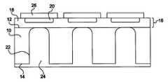
- substrate 10includes first main surface 12 and second main surface 14 opposing first main surface 12 .
- First and second main surfaces 12 and 14may be respectively characterized as front and back sides of substrate 10 , whereby devices are disposed on or over the first main surface 12 or front side of substrate 10 .
- Substrate 10is silicon carbide and has n-type conductivity, and may have a thickness of about 300 to 500 ⁇ m, or about 400 ⁇ m.
- Substrate 10however should not necessarily be limited as silicon carbide, or as having n-type conductivity, but may be other materials such as silicon or sapphire.
- active epitaxial layers 16having an overall thickness of about 1 ⁇ m are disposed on first main surface 12 of substrate 10 .
- Active device layers 16include a first aluminum gallium nitride (Al x Ga 1-x N, hereinafter referred to as AlGaN) layer 18 on or over first main surface 12 and doped so as to have a first conductivity type, and second AlGaN layers 20 on or within AlGaN layer 18 and doped so as to have a second conductivity type opposite to the first conductivity type.
- AlGaN layer 18 and AlGaN layers 20form respective p-n junctions.
- AlGaN layer 18is doped n-type with silicon for instance, and AlGaN layer 20 is doped p-type with magnesium for instance.
- Active epitaxial layers 16may however include silicon carbide or gallium nitride (hereinafter referred to as GaN) layers in addition to AlGaN layers, or combinations of these layers.
- Substrate 10 as shown in FIG. 1includes a plurality of dimples 22 formed therein, each of which extending from second main surface 14 through substrate 10 to active expitaxial layers 16 , whereby a dimple 22 is disposed for each respective p-n junction formed by AlGaN layers 18 and 20 .
- Each dimple 22extends entirely through substrate 10 to active epitaxial layers 16 .
- dimples 22may be disposed so as not to extend entirely through substrate 10 .
- dimpled substrate 10allows direct contact to AlGaN layer 18 , direct contact is realized without a heterojunction formed between silicon carbide and AlGaN layer 18 .
- AlGaN layers 18 and 20may in the alternative be respectively doped to have p-type conductivity and n-type conductivity.
- Electrical contact 24is disposed on second main surface 14 of substrate 10 and within dimples 22 , to thus contact active epitaxial layers 16 exposed within dimples 22 . Electrical contact 24 is shown as completely filling dimples 22 . However, electrical contact 24 may alternatively be disposed conformally as a layer on second main surface 14 of substrate 10 and on the surfaces within dimples 22 , and as having prescribed thickness such as 1 ⁇ m. Electrical contact 24 is a material having low electrical resistance as compared to substrate 10 .
- Electrical contact 24may be metallization such as titanium, aluminium, copper or tungsten; silicides such as TiSi x or NiSi x ; nitrides such as TiN or WN x ; combinations thereof; or polysilicon, amorphous silicon, or any other suitable contact material having low electrical resistance.
- Respective electrical contacts 26are provided on or above AlGaN layers 20 , and may be the same metallization as electrical contact 24 , or any suitable contact material.
- the substratecontributes about 60% of the overall on-resistance of the device, whereas a dimpled substrate of a 300V Schottky diode contributes about 30% of the overall on-resistance of the device.
- a vertical 600V Schottky diodethe contribution of the substrate to the overall on-resistance of the device is reduced from about 30% to about 15% using dimpled substrate contacts
- a vertical 1200V Schottky diodethe contribution of the substrate to the overall on-resistance of the device is reduced from about 15% to about 7.5% using dimpled substrate contacts.
- active epitaxial layers 16are described as including p-n junctions consisting of first and second AlGaN layers 18 and 20 that are doped so as to have different respective conductivity type. Accordingly, each of the active regions may be power devices such as diodes, Schottky diodes or light emitting diodes (LEDs).
- the devices made up of active epitaxial layers 16 in FIG. 1should not be limited merely to AlGaN layered p-n junction devices.
- active epitaxial layers 16may be epitaxially grown silicon carbide layers having different respective conductivity type.
- the devices made up of active epitaxial layers 16may also include MOSFETs, BJTs, n-channel IGBTs, thyristors and/or vertical JFETs, or other various devices. Electrical contact is provided to the devices from the back side or second main surface of a substrate such as silicon carbide in a vertical manner through dimples, so that devices with excellent thermal conductivity and low resistance contact are realized.
- FIG. 1shows three separate p-n junctions within active epitaxial layers 16 and three corresponding dimples 22
- the number and disposition of dimples 22 within substrate 10should not be necessarily limited as shown.
- a single dimple, or any number of dimplesmay be formed in substrate 10 .
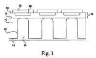
- FIG. 2shows a partial perspective view of the back side of substrate 10 including a two-dimensional regular array of dimples 22 , which are in part depicted by dashed ghost lines.
- Dimples 22are shown as extending from second main surface 14 , through substrate 10 to first main surface 12 , to be in contact with active epitaxial layers 16 which include first and second AlGaN layers 18 and 20 consistent with FIG. 1 .
- Dimples 22 as depicted by the ghost linesare shown as oval in shape, and may have a diameter of between about 10 ⁇ m and 1 mm. In the alternative, dimples 22 may be circular in shape. Moreover, dimples 22 of the regular array may be disposed along directions parallel to a specific crystallographic direction (such as 11-20 or 1-100 directions) of substrate 10 , to aid in stress relief and help prevent breakage of substrate 10 . Alternatively, dimples 22 may be disposed randomly within an array.
- dimples 30are shown as extending from second main surface 14 through substrate 10 toward first main surface 12 .
- Active epitaxial layers 16are shown as a single layer, but should be understood as including multiple layers of various different epitaxial layers that can make up various different devices as described with respect to FIG. 1 , but which are omitted in FIG. 3 (and also in FIGS. 4-6 ) for the sake of simplicity.
- Contact layer 28is shown on or above active epitaxial layers 16 , and in a subsequent step may be patterned if necessary to form respective electrical contacts such as contacts 26 shown in FIG. 1 .
- a silicon dioxide mask 40is shown as disposed on second main surface 14 of substrate 10 .
- FIG. 3chemical etching is carried out using silicon dioxide mask 40 to form dimples 30 .
- substrate 10is silicon carbide.
- a high temperature Cl 2 /O 2 gas mixtureis used as an etchant to form dimples 30 under the following conditions for example: 800° C., 10% Cl 2 in oxygen.
- Substrate 10is thus etched substantially isotropically, whereby dimples 30 are formed as having a somewhat broad shape with gradual sloped sidewalls.
- An advantage of chemical etching as described with respect to FIG. 3is that dimples having such broad shape with gradually sloped sidewalls are easy to metallize.
- etching of silicon carbide using purely chemical meansmay be difficult, the chemical composition of the etchants used to etch silicon carbide substrate 10 in connection with the embodiment described with respect to FIG. 3 may be varied.
- Ar or He or other reactive gasessuch as group VII elements F or Br may be added to the etchant gas.
- substrate 10should not necessarily be limited as silicon carbide, and since various other substrate materials may be used, it should likewise be understood that a variety of chemical etchants suitable for specific various materials may be utilized.
- mask 40is described as being silicon dioxide, other mask materials such as other oxide or nitride dielectrics (Al 2 O 3 , SiN x ) may be used as appropriate.
- dimples 32are shown as extending from second main surface 14 through substrate 10 toward first main surface 12 .
- Active epitaxial layers 16are shown as a single layer, but should be understood as including multiple layers of various different epitaxial layers that can make up various different devices as described with respect to FIG. 1 .
- Contact layer 28is on or above active epitaxial layers 16 , and in a subsequent step may be patterned if necessary to form respective electrical contacts such as contacts 26 shown in FIG. 1 .
- metal mask 42is disposed on second main surface 14 of substrate 10 .
- plasma etching using for example high density plasmasis carried out using metal mask 42 , to form dimples 32 .
- Substrate 10is silicon carbide, and the plasma etching may be carried out using Fl based gases SF 6 , CHF 3 or CF 4 , for example.
- Substrate 10is thus etched predominantly anisotropically, and is thus shown as having a profile that is somewhat narrower than as shown in FIG. 3 and which has steeper sidewalls.
- substrate 10should not necessarily be limited to silicon carbide, and since other various substrate materials may be used, it should likewise be understood that a variety of plasma etchant systems suitable for specific various materials may be utilized.
- laser ablationis carried out to form dimples 34 , without utilizing a mask.
- a YAG laserfor example, which is commonly used for wafer marking to burn an identity number, may be tuned to ablate substrate 10 to form dimples 34 .
- a variety of ablation parameterssuch as absorption of laser light and heat conductivity of the material to be ablated must be taken into consideration.
- silicon carbideis an extremely inert material that conducts heat very well. For example, selection of a wavelength with minimum absorption depth will help to ensure high energy deposition in a small volume for rapid and complete ablation. Selection of a short pulse duration will help to maximize peak power, and minimize thermal conduction to the substrate or work material surrounding the targeted ablation zone.
- pulse repetition rateis also important. A more rapid pulse repetition rate will help to retain residual heat in the ablation zone, limiting the time for conduction and thus increasing efficiency of laser ablation. In other words, more of the incident energy will contribute to ablation and less will be lost to the substrate, work material or environment. Beam quality is also an important factor, and may be controlled in terms of brightness (energy), focusability, and homogeneity. The beam should be of controlled size, so that the ablation zone is not larger than desired, to thus prevent formation of dimples with excessively sloped sidewalls.
- substrate 10is silicon carbide.
- a KrF excimer laser(wavelength 248 nm) for example may be used for laser ablation under the following conditions: typical pulse width in the range of 10-100 ns and a repetition rate of 1-50 Hz, whereby the laser beam is focused to give an energy density in the range of 5-50 cm ⁇ 2 .
- Dimples 34 as shown in FIG. 5are thus provided as having highly controlled shape and side wall slope. Moreover, processing is simplified, faster and more efficient, whereby mask formation, mask patterning and mask removal steps are eliminated.
- the dimples in generalmay be circular or oval in shape.
- the shape of the dimplesis not limited.
- dimples as formed by laser ablation in connection with FIG. 5would be circular or oval shaped, as defined by beam profile.
- the dimplesmay also be square, rectangular, or triangular shaped, or any other shape as desired, as defined by masks 40 and 42 used in connection with FIGS. 3 and 4 respectively.
- the dimplesmay also be irregularly shaped of various length and/or width.
- dimple diametermay be in the range of about 10 ⁇ m and 1 mm.
- the dimpleshave a depth from first main surface 14 as shown in FIG. 1 that is at least about half the thickness of substrate 10 , for example. However, it should be understood that dimple depth may be selected as desired, and may be less than about half the thickness of the corresponding substrate if desired.
- etch stop layer 38as disposed on first main substrate 10 may be gallium nitride.
- dimples 36are shown as extending from second main surface 14 through substrate 10 toward first main surface 12 .
- Active epitaxial layers 16are shown as a single layer disposed on etch stop layer 38 , but should be understood as including multiple layers of various different materials that make up various different devices as described with respect to FIG. 1 .
- Contact layer 28is shown on or above active epitaxial layers 16 , and in a subsequent step may be patterned if necessary to form respective electrical contacts such as contacts 26 shown in FIG. 1 . Also, a metal mask 42 is shown as disposed on second main surface 14 of substrate 10 .
- substrate 10 and etch stop layer 38are respectively silicon carbide and gallium nitride.
- a fluorine based etch chemistrysuch as SF 6 , CF 4 or CHF 3 having high etch selectively with respect to silicon carbide and gallium nitride may be used, so that silicon carbide substrate 10 is etched at a significantly higher rate than etch stop layer 38 .
- Use of etch stop layer 38 as describedsimplifies dimple formation and improves accuracy and efficiency. It should also be understood that the use of silicon carbide, gallium nitride and the above noted etchants should not be considered as limiting.
- Various substrate materials, etchants and corresponding suitable etch stop layersmay be respectively utilized.
- FIG. 7illustrates a variation of the structure described with respect to FIG. 1 , wherein FIG. 7 includes dimples 42 overgrown with additional silicon carbide epitaxy.
- active epitaxial layers 60are shown as grown on first main surface 12 of substrate 70 , whereby substrate 70 is n-type silicon carbide and has a thickness of about 300 to 500 ⁇ m, or about 400 ⁇ m.
- Active epitaxial layers 60have an overall thickness of at least about 50 ⁇ m, or about 100 ⁇ m.
- Active epitaxial layers 60include first SiC layer 62 doped to have n-type conductivity and epitaxially grown on first main surface 12 of SiC substrate 70 , and second SiC layers 64 doped to have p-type conductivity and grown on or in first SiC layer 62 .
- dimples 42are formed first by chemical etching, dry plasma etching or laser ablation as described previously, to extend entirely through substrate 70 .
- Respective electrical contacts 26are provided on or above active epitaxial layers 60 , and may be metallization such as nickel, titanium or tungsten.
- Silicon carbide epitaxial layer 44may be formed by Metal Organic Chemical Vapor Deposition (MOCVD) using standard process conditions. Silicon carbide epitaxial layer 44 may have a thickness of about 1 ⁇ m. In this structure, additional p-type silicon carbide epitaxial layer 44 has been added so that substrate 10 may in effect have the function of a p-type substrate.
- MOCVDMetal Organic Chemical Vapor Deposition
- substrate 10includes first main surface 12 having etch stop layer 38 thereon. Active epitaxial layers and electrical contacts (not shown for simplicity) are formed over etch stop layer 38 .
- substrate 10is silicon carbide and etch stop layer 38 is gallium nitride, although other suitable substrate and etch stop materials may be used.
- Dimples 46extend from second main surface 14 through substrate 10 toward first main surface 12 , and may be formed in a first stage by chemical etching or laser ablation as previously described. However, the shape of dimples 46 in FIGS.
- FIG. 8A-8Cshould be considered as general, and the shape does not imply that the dimples are formed specifically by chemical etching or laser ablation.
- FIG. 8Ais shown after mask removal. Dimple formation in FIG. 8A is controlled so that dimples 46 do not extend entirely through substrate 10 , such control being well within the level of ordinary skill. For example, for a substrate 10 having thickness of about 350 ⁇ m, dimples 46 may have a depth of about 300 ⁇ m.
- a subsequent selective dry etchingis carried out using etch stop layer 38 , to thereby form vias 48 through the remaining portion of substrate 10 between dimples 46 and first main surface 12 .
- This subsequent dry etchingmay be carried out using conditions similar to those previously described for the formation of dimples. In this case, a mask is not necessary because etching of the surrounding non-dimpled substrate will not adversely effect the performance of the substrate.
- electrical contact 24is formed on second main surface 14 and within vias 48 and dimples 46 as shown in FIG. 8C .
- a more controlled etch ratecan be implemented in the second step, increasing the selectivity of the etching process.
- the slope of the sidewallsmay be controlled by this two step process, to aid in metallization of the dimples.
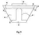
- FIG. 9illustrates an LED chip constructed as including a dimpled substrate.
- the LED chipincludes substrate 50 having first main surface 56 , and second main surface 58 opposing first main surface 56 .
- First and second main surfaces 56 and 58may be respectively characterized as front and back sides of substrate 50 .
- Substrate 50 in this caseis transparent silicon carbide and may have a thickness of about 300-500 microns, or about 400 microns, but may have other various thicknesses.
- Active epitaxial layers 80are disposed on first main surface 56 of transparent substrate 50 , as further shown in FIG. 9 .
- Active epitaxial layers 80include GaN layer 82 doped so as to have a first conductivity type and epitaxially grown on first main surface 56 , and AlGaN layer 84 doped so as to have a second conductivity type opposite the first conductivity type and epitaxially grown on GaN layer 82 .
- GaN layer 82has n-type conductivity and AlGaN layer 84 has p-type conductivity, although layers 82 and 84 may in the alternative be doped to respectively have p-type and n-type conductivities.
- Dimple 48is formed within transparent substrate 50 as shown in FIG. 9 , extending from second main surface 58 through to first main surface 56 .
- Dimple 48may be formed by chemical etching, dry plasma etching, laser ablation or a combination thereof as previously described.
- Dimple 48extends entirely through transparent substrate 50 , but in the alternative may extend partly therethrough so that a portion of transparent substrate 50 remains between dimple 48 and active epitaxial layers 80 .
- Electrical contact 24is formed on second main surface 58 and within dimple 48 .
- electrical contact 24may be disposed conformally as a layer on second main surface 58 and within dimple 48 , so as not to entirely bury or fill dimple 48 .
- Electrical contact 24may be materials such as described previously.
- the LED chipas shown in FIG.
- FIG. 9may be initially formed on a wafer including a plurality of like formed LEDs, whereby the wafer is then cut to form single LED chips as shown in FIG. 9 .
- Sidewalls 52 of transparent substrate 50are shown as cut to be gradually sloped, so that internal reflection of generated light helps to increase efficiency of the LED. It should however be understood that sidewalls 52 may also be cut to be substantially vertical.
Landscapes
- Engineering & Computer Science (AREA)
- Manufacturing & Machinery (AREA)
- Physics & Mathematics (AREA)
- Crystallography & Structural Chemistry (AREA)
- Condensed Matter Physics & Semiconductors (AREA)
- General Physics & Mathematics (AREA)
- Chemical & Material Sciences (AREA)
- Computer Hardware Design (AREA)
- Microelectronics & Electronic Packaging (AREA)
- Power Engineering (AREA)
- Electrodes Of Semiconductors (AREA)
- Internal Circuitry In Semiconductor Integrated Circuit Devices (AREA)
- Led Devices (AREA)
- Laminated Bodies (AREA)
Abstract
Description
- The present application claims the benefit of priority under 35 U.S.C. 119(e)(1) to U.S. Provisional Patent Application No. 60/757,481 entitled “SiC DIMPLED SUBSTRATE”, filed Jan. 10, 2006, which is hereby incorporated by reference in its entirety for all purposes.
- 1. Field of the Invention
- This invention relates generally to microelectronic devices, and more particularly to silicon carbide power devices and LEDs.
- 2. Description of the Background Art
- Silicon carbide has relatively high thermal conductivity, and thus has been used as a substrate for high power devices and LEDs. However, because of the low mobility of silicon carbide and the incomplete ionization of impurities in silicon carbide, silicon carbide substrates used as back contacts in vertical devices have high resistance. For example, the substrate of a silicon carbide 300V Schottky diode contributes about two-thirds of the overall on-resistance of the device. A conventional approach to reduce parasitic loss due to substrate resistance involves the removal or thinning of substrate material. However, in the case of silicon carbide substrates, this approach can be considered disadvantageous, because it entails removal of silicon carbide which is an effective heat sink. Thus, a technology is sought to provide a substrate that is an effective heat sink, but that has a low resistance back contact that does not contribute significant loss during device operation.
- The present invention is therefore directed to a device and method which substantially overcomes one or more of the problems due to the limitations and disadvantages of the related art.
- An object of the invention is to thus provide a semiconductor device including a silicon carbide substrate having a first main surface and a second main surface opposing the first main surface; an active epitaxial device layer on the first main surface of the silicon carbide substrate; a dimple extending from the second main surface into the silicon carbide substrate toward the first main surface; a first electrical contact on the active epitaxial device layer; and a second electrical contact overlying the second main surface and within the dimple.
- A further object of the invention is to provide a method of forming a semiconductor device including epitaxially growing an active device layer on a first main surface of a silicon carbide substrate, the silicon carbide substrate having a second main surface opposing the first main surface; forming at least one dimple extending from the second main surface into the silicon carbide substrate toward the first main surface; forming a first electrical contact over the active device layer; and forming a second electrical contact overlying the second main surface and within the at least one dimple.
- A still further object is to provide a substrate including a silicon carbide layer having a first main surface and a second main surface opposing the first main surface; an AlxGa1-xN layer on the first main surface of the silicon carbide layer; an array of dimples extending from the second main surface into the silicon carbide substrate toward the first main surface; and a metallization layer overlying the second main surface of the silicon carbide layer and within the dimples.
- The present invention will become more fully understood from the detailed description given herein below and the accompanying drawings which are given by way of illustration only, and thus are not limitative of the present invention, and wherein:
FIG. 1 illustrates a multiple contact device with dimpled substrate;FIG. 2 illustrates a partial perspective view of the back side of the device ofFIG. 1 , with arrayed dimples;FIG. 3 illustrates a dimpled substrate as formed by chemical etching;FIG. 4 illustrates a dimpled substrate as formed by dry plasma etching;FIG. 5 illustrates a dimpled substrate as formed by laser ablation;FIG. 6 illustrates a dimpled substrate as formed by chemical etching and using an etch stop layer;FIG. 7 illustrates a multiple contact device with additional epitaxy overgrowth within the dimples;FIGS. 8A-8C illustrate a two-stage process of dimple formation; andFIG. 9 illustrates an LED chip construction with transparent substrate.- The invention will now be described more fully hereinafter with reference to the accompanying drawings, in which preferred embodiments of the invention are shown. However, this invention should not be construed as limited to the embodiments set forth herein. Rather, these embodiments are provided so that this disclosure will be thorough and complete, and will fully convey the scope of the invention to those skilled in the art. In the drawings, the thicknesses of layers and regions are exaggerated for clarity. Like numbers refer to like elements throughout.
- As shown in
FIG. 1 ,substrate 10 includes firstmain surface 12 and secondmain surface 14 opposing firstmain surface 12. First and secondmain surfaces substrate 10, whereby devices are disposed on or over the firstmain surface 12 or front side ofsubstrate 10.Substrate 10 is silicon carbide and has n-type conductivity, and may have a thickness of about 300 to 500 μm, or about 400 μm.Substrate 10 however should not necessarily be limited as silicon carbide, or as having n-type conductivity, but may be other materials such as silicon or sapphire. - As further shown in
FIG. 1 , activeepitaxial layers 16 having an overall thickness of about 1 μm are disposed on firstmain surface 12 ofsubstrate 10.Active device layers 16 include a first aluminum gallium nitride (AlxGa1-xN, hereinafter referred to as AlGaN)layer 18 on or over firstmain surface 12 and doped so as to have a first conductivity type, andsecond AlGaN layers 20 on or withinAlGaN layer 18 and doped so as to have a second conductivity type opposite to the first conductivity type. AlGaNlayer 18 andAlGaN layers 20 form respective p-n junctions. AlGaNlayer 18 is doped n-type with silicon for instance, and AlGaNlayer 20 is doped p-type with magnesium for instance. Activeepitaxial layers 16 may however include silicon carbide or gallium nitride (hereinafter referred to as GaN) layers in addition to AlGaN layers, or combinations of these layers. Substrate 10 as shown inFIG. 1 includes a plurality ofdimples 22 formed therein, each of which extending from secondmain surface 14 throughsubstrate 10 to activeexpitaxial layers 16, whereby adimple 22 is disposed for each respective p-n junction formed byAlGaN layers dimple 22 extends entirely throughsubstrate 10 to activeepitaxial layers 16. As will be subsequently described,dimples 22 may be disposed so as not to extend entirely throughsubstrate 10. Of note, sincedimpled substrate 10 allows direct contact to AlGaNlayer 18, direct contact is realized without a heterojunction formed between silicon carbide andAlGaN layer 18. As a result,AlGaN layers Electrical contact 24 is disposed on secondmain surface 14 ofsubstrate 10 and withindimples 22, to thus contact activeepitaxial layers 16 exposed withindimples 22.Electrical contact 24 is shown as completely fillingdimples 22. However,electrical contact 24 may alternatively be disposed conformally as a layer on secondmain surface 14 ofsubstrate 10 and on the surfaces withindimples 22, and as having prescribed thickness such as 1 μm.Electrical contact 24 is a material having low electrical resistance as compared tosubstrate 10.Electrical contact 24 may be metallization such as titanium, aluminium, copper or tungsten; silicides such as TiSixor NiSix; nitrides such as TiN or WNx; combinations thereof; or polysilicon, amorphous silicon, or any other suitable contact material having low electrical resistance. Respectiveelectrical contacts 26 are provided on or aboveAlGaN layers 20, and may be the same metallization aselectrical contact 24, or any suitable contact material.- As should be understood in view of
FIG. 1 , access to active devices on the front side of firstmain surface 12 is provided from the back side or secondmain surface 14 ofsubstrate 10, throughdimples 22. Thus, direct electrical contact to devices made up of activeepitaxial layers 16 is provided, while substantially eliminating serial resistance contributed bysubstrate 10 and while maintaining excellent overall thermal conductivity due to the use of silicon carbide as substrate material. This is provided without the necessity of thinningsubstrate 10 as conventionally done, thus reducing manufacturing expense and complexity while improving performance. As noted above, silicon carbide substrates when used as an electrical carrier contribute significantly to the overall on-resistance of a device. The use of dimpled substrates as in this embodiment should cut the contribution of substrate resistance. As an example, for a conventional vertical 300V Schottky diode, the substrate contributes about 60% of the overall on-resistance of the device, whereas a dimpled substrate of a 300V Schottky diode contributes about 30% of the overall on-resistance of the device. Similarly, for a vertical 600V Schottky diode the contribution of the substrate to the overall on-resistance of the device is reduced from about 30% to about 15% using dimpled substrate contacts, and for a vertical 1200V Schottky diode the contribution of the substrate to the overall on-resistance of the device is reduced from about 15% to about 7.5% using dimpled substrate contacts. - In
FIG. 1 , activeepitaxial layers 16 are described as including p-n junctions consisting of first andsecond AlGaN layers epitaxial layers 16 inFIG. 1 should not be limited merely to AlGaN layered p-n junction devices. For example, active epitaxial layers16 may be epitaxially grown silicon carbide layers having different respective conductivity type. Moreover, the devices made up of activeepitaxial layers 16 may also include MOSFETs, BJTs, n-channel IGBTs, thyristors and/or vertical JFETs, or other various devices. Electrical contact is provided to the devices from the back side or second main surface of a substrate such as silicon carbide in a vertical manner through dimples, so that devices with excellent thermal conductivity and low resistance contact are realized. - Moreover, although
FIG. 1 shows three separate p-n junctions within active epitaxial layers16 and three correspondingdimples 22, the number and disposition ofdimples 22 withinsubstrate 10 should not be necessarily limited as shown. A single dimple, or any number of dimples may be formed insubstrate 10. For example,FIG. 2 shows a partial perspective view of the back side ofsubstrate 10 including a two-dimensional regular array ofdimples 22, which are in part depicted by dashed ghost lines.Dimples 22 are shown as extending from secondmain surface 14, throughsubstrate 10 to firstmain surface 12, to be in contact with activeepitaxial layers 16 which include first and second AlGaN layers18 and20 consistent withFIG. 1 .Dimples 22 as depicted by the ghost lines are shown as oval in shape, and may have a diameter of between about 10 μm and 1 mm. In the alternative, dimples22 may be circular in shape. Moreover, dimples22 of the regular array may be disposed along directions parallel to a specific crystallographic direction (such as 11-20 or 1-100 directions) ofsubstrate 10, to aid in stress relief and help prevent breakage ofsubstrate 10. Alternatively, dimples22 may be disposed randomly within an array. - Dimple formation and different respective dimple profiles are next described with reference to
FIGS. 3-6 . InFIG. 3 , dimples30 are shown as extending from secondmain surface 14 throughsubstrate 10 toward firstmain surface 12. Active epitaxial layers16 are shown as a single layer, but should be understood as including multiple layers of various different epitaxial layers that can make up various different devices as described with respect toFIG. 1 , but which are omitted inFIG. 3 (and also inFIGS. 4-6 ) for the sake of simplicity.Contact layer 28 is shown on or above active epitaxial layers16, and in a subsequent step may be patterned if necessary to form respective electrical contacts such ascontacts 26 shown inFIG. 1 . Also, asilicon dioxide mask 40 is shown as disposed on secondmain surface 14 ofsubstrate 10. - In
FIG. 3 , chemical etching is carried out usingsilicon dioxide mask 40 to form dimples30. As noted,substrate 10 is silicon carbide. A high temperature Cl2/O2gas mixture is used as an etchant to formdimples 30 under the following conditions for example: 800° C., 10% Cl2in oxygen.Substrate 10 is thus etched substantially isotropically, whereby dimples30 are formed as having a somewhat broad shape with gradual sloped sidewalls. An advantage of chemical etching as described with respect toFIG. 3 is that dimples having such broad shape with gradually sloped sidewalls are easy to metallize. - It should be understood that although the etching of silicon carbide using purely chemical means may be difficult, the chemical composition of the etchants used to etch
silicon carbide substrate 10 in connection with the embodiment described with respect toFIG. 3 may be varied. For example, Ar or He or other reactive gases such as group VII elements F or Br may be added to the etchant gas. Also, sincesubstrate 10 should not necessarily be limited as silicon carbide, and since various other substrate materials may be used, it should likewise be understood that a variety of chemical etchants suitable for specific various materials may be utilized. Also, althoughmask 40 is described as being silicon dioxide, other mask materials such as other oxide or nitride dielectrics (Al2O3, SiNx) may be used as appropriate. - In
FIG. 4 , dimples32 are shown as extending from secondmain surface 14 throughsubstrate 10 toward firstmain surface 12. Active epitaxial layers16 are shown as a single layer, but should be understood as including multiple layers of various different epitaxial layers that can make up various different devices as described with respect toFIG. 1 .Contact layer 28 is on or above active epitaxial layers16, and in a subsequent step may be patterned if necessary to form respective electrical contacts such ascontacts 26 shown inFIG. 1 . Also,metal mask 42 is disposed on secondmain surface 14 ofsubstrate 10. - In
FIG. 4 , plasma etching using for example high density plasmas (such as ICP) is carried out usingmetal mask 42, to form dimples32.Substrate 10 is silicon carbide, and the plasma etching may be carried out using Fl based gases SF6, CHF3or CF4, for example.Substrate 10 is thus etched predominantly anisotropically, and is thus shown as having a profile that is somewhat narrower than as shown inFIG. 3 and which has steeper sidewalls. - It should be understood that various other suitable plasma etching conditions may be used to etch
silicon carbide substrate 10 in connection withFIG. 4 . Sincesubstrate 10 should not necessarily be limited to silicon carbide, and since other various substrate materials may be used, it should likewise be understood that a variety of plasma etchant systems suitable for specific various materials may be utilized. - In
FIG. 5 , laser ablation is carried out to formdimples 34, without utilizing a mask. A YAG laser for example, which is commonly used for wafer marking to burn an identity number, may be tuned to ablatesubstrate 10 to form dimples34. A variety of ablation parameters such as absorption of laser light and heat conductivity of the material to be ablated must be taken into consideration. In greater detail, it is known that silicon carbide is an extremely inert material that conducts heat very well. For example, selection of a wavelength with minimum absorption depth will help to ensure high energy deposition in a small volume for rapid and complete ablation. Selection of a short pulse duration will help to maximize peak power, and minimize thermal conduction to the substrate or work material surrounding the targeted ablation zone. Selection of pulse repetition rate is also important. A more rapid pulse repetition rate will help to retain residual heat in the ablation zone, limiting the time for conduction and thus increasing efficiency of laser ablation. In other words, more of the incident energy will contribute to ablation and less will be lost to the substrate, work material or environment. Beam quality is also an important factor, and may be controlled in terms of brightness (energy), focusability, and homogeneity. The beam should be of controlled size, so that the ablation zone is not larger than desired, to thus prevent formation of dimples with excessively sloped sidewalls. - In
FIG. 5 substrate 10 is silicon carbide. In this case, a KrF excimer laser (wavelength 248 nm) for example may be used for laser ablation under the following conditions: typical pulse width in the range of 10-100 ns and a repetition rate of 1-50 Hz, whereby the laser beam is focused to give an energy density in the range of 5-50 cm−2. However, it should be understood that various other laser types and/or parameters as appropriate may be used.Dimples 34 as shown inFIG. 5 are thus provided as having highly controlled shape and side wall slope. Moreover, processing is simplified, faster and more efficient, whereby mask formation, mask patterning and mask removal steps are eliminated. - As previously described, the dimples in general may be circular or oval in shape. However, the shape of the dimples is not limited. For example, dimples as formed by laser ablation in connection with
FIG. 5 would be circular or oval shaped, as defined by beam profile. However, the dimples may also be square, rectangular, or triangular shaped, or any other shape as desired, as defined bymasks FIGS. 3 and 4 respectively. The dimples may also be irregularly shaped of various length and/or width. As previously described, dimple diameter may be in the range of about 10 μm and 1 mm. Typically, the dimples have a depth from firstmain surface 14 as shown inFIG. 1 that is at least about half the thickness ofsubstrate 10, for example. However, it should be understood that dimple depth may be selected as desired, and may be less than about half the thickness of the corresponding substrate if desired. - In a variation of the process described with respect to
FIG. 4 , plasma based chemical etching is carried out inFIG. 6 usingmask 42 andetch stop layer 38. Forsubstrate 10 made of silicon carbide,etch stop layer 38 as disposed on firstmain substrate 10 may be gallium nitride. InFIG. 6 , dimples36 are shown as extending from secondmain surface 14 throughsubstrate 10 toward firstmain surface 12. Active epitaxial layers16 are shown as a single layer disposed onetch stop layer 38, but should be understood as including multiple layers of various different materials that make up various different devices as described with respect toFIG. 1 .Contact layer 28 is shown on or above active epitaxial layers16, and in a subsequent step may be patterned if necessary to form respective electrical contacts such ascontacts 26 shown inFIG. 1 . Also, ametal mask 42 is shown as disposed on secondmain surface 14 ofsubstrate 10. - In
FIG. 6 , plasma based chemical etching is carried out usingmask 42 andetch stop layer 38, so thatdimples 36 extend all the way to etchstop layer 38. As noted above,substrate 10 andetch stop layer 38 are respectively silicon carbide and gallium nitride. A fluorine based etch chemistry such as SF6, CF4or CHF3having high etch selectively with respect to silicon carbide and gallium nitride may be used, so thatsilicon carbide substrate 10 is etched at a significantly higher rate thanetch stop layer 38. Use ofetch stop layer 38 as described simplifies dimple formation and improves accuracy and efficiency. It should also be understood that the use of silicon carbide, gallium nitride and the above noted etchants should not be considered as limiting. Various substrate materials, etchants and corresponding suitable etch stop layers may be respectively utilized. FIG. 7 illustrates a variation of the structure described with respect toFIG. 1 , whereinFIG. 7 includesdimples 42 overgrown with additional silicon carbide epitaxy. InFIG. 7 , active epitaxial layers60 are shown as grown on firstmain surface 12 ofsubstrate 70, wherebysubstrate 70 is n-type silicon carbide and has a thickness of about 300 to 500 μm, or about 400 μm. Active epitaxial layers60 have an overall thickness of at least about 50 μm, or about 100 μm. Active epitaxial layers60 includefirst SiC layer 62 doped to have n-type conductivity and epitaxially grown on firstmain surface 12 ofSiC substrate 70, and second SiC layers64 doped to have p-type conductivity and grown on or infirst SiC layer 62. Initially, dimples42 are formed first by chemical etching, dry plasma etching or laser ablation as described previously, to extend entirely throughsubstrate 70. Respectiveelectrical contacts 26 are provided on or above active epitaxial layers60, and may be metallization such as nickel, titanium or tungsten.- Prior to formation of
electrical contact 24 shown inFIG. 7 , dimples42 and secondmain surface 14 ofsilicon carbide substrate 70 are overgrown with an additional siliconcarbide epitaxial layer 44. Siliconcarbide epitaxial layer 44 may be formed by Metal Organic Chemical Vapor Deposition (MOCVD) using standard process conditions. Siliconcarbide epitaxial layer 44 may have a thickness of about 1 μm. In this structure, additional p-type siliconcarbide epitaxial layer 44 has been added so thatsubstrate 10 may in effect have the function of a p-type substrate. - A two-stage process of dimple formation is next described in connection with
FIGS. 8A-8C . As shown inFIG. 8A ,substrate 10 includes firstmain surface 12 having etch stoplayer 38 thereon. Active epitaxial layers and electrical contacts (not shown for simplicity) are formed overetch stop layer 38. As previously described,substrate 10 is silicon carbide andetch stop layer 38 is gallium nitride, although other suitable substrate and etch stop materials may be used.Dimples 46 extend from secondmain surface 14 throughsubstrate 10 toward firstmain surface 12, and may be formed in a first stage by chemical etching or laser ablation as previously described. However, the shape ofdimples 46 inFIGS. 8A-8C should be considered as general, and the shape does not imply that the dimples are formed specifically by chemical etching or laser ablation. In the case wherein dimple formation is by chemical etching,FIG. 8A is shown after mask removal. Dimple formation inFIG. 8A is controlled so thatdimples 46 do not extend entirely throughsubstrate 10, such control being well within the level of ordinary skill. For example, for asubstrate 10 having thickness of about 350 μm, dimples46 may have a depth of about 300 μm. - As shown in
FIG. 8B , a subsequent selective dry etching is carried out usingetch stop layer 38, to thereby formvias 48 through the remaining portion ofsubstrate 10 betweendimples 46 and firstmain surface 12. This subsequent dry etching may be carried out using conditions similar to those previously described for the formation of dimples. In this case, a mask is not necessary because etching of the surrounding non-dimpled substrate will not adversely effect the performance of the substrate. Thereafter,electrical contact 24 is formed on secondmain surface 14 and withinvias 48 anddimples 46 as shown inFIG. 8C . As a result of dimple formation in this two step process, a more controlled etch rate can be implemented in the second step, increasing the selectivity of the etching process. Also, the slope of the sidewalls may be controlled by this two step process, to aid in metallization of the dimples. FIG. 9 illustrates an LED chip constructed as including a dimpled substrate. As shown inFIG. 9 , the LED chip includessubstrate 50 having firstmain surface 56, and secondmain surface 58 opposing firstmain surface 56. First and secondmain surfaces substrate 50.Substrate 50 in this case is transparent silicon carbide and may have a thickness of about 300-500 microns, or about 400 microns, but may have other various thicknesses.- Active epitaxial layers80 are disposed on first
main surface 56 oftransparent substrate 50, as further shown inFIG. 9 . Active epitaxial layers80 includeGaN layer 82 doped so as to have a first conductivity type and epitaxially grown on firstmain surface 56, andAlGaN layer 84 doped so as to have a second conductivity type opposite the first conductivity type and epitaxially grown onGaN layer 82.GaN layer 82 has n-type conductivity andAlGaN layer 84 has p-type conductivity, althoughlayers Dimple 48 is formed withintransparent substrate 50 as shown inFIG. 9 , extending from secondmain surface 58 through to firstmain surface 56.Dimple 48 may be formed by chemical etching, dry plasma etching, laser ablation or a combination thereof as previously described.Dimple 48 extends entirely throughtransparent substrate 50, but in the alternative may extend partly therethrough so that a portion oftransparent substrate 50 remains betweendimple 48 and active epitaxial layers80.Electrical contact 24 is formed on secondmain surface 58 and withindimple 48. In the alternative,electrical contact 24 may be disposed conformally as a layer on secondmain surface 58 and withindimple 48, so as not to entirely bury or filldimple 48.Electrical contact 24 may be materials such as described previously. The LED chip as shown inFIG. 9 may be initially formed on a wafer including a plurality of like formed LEDs, whereby the wafer is then cut to form single LED chips as shown inFIG. 9 .Sidewalls 52 oftransparent substrate 50 are shown as cut to be gradually sloped, so that internal reflection of generated light helps to increase efficiency of the LED. It should however be understood that sidewalls52 may also be cut to be substantially vertical.- The invention being thus described, it will be obvious that the same may be varied in many ways. Such variations are not be to regarded as a departure from the spirit and scope of the invention, and all such modifications as would be obvious to one skilled in the art are intended to be included within the scope of the following claims.
Claims (40)
Priority Applications (1)
| Application Number | Priority Date | Filing Date | Title |
|---|---|---|---|
| US11/651,528US8664664B2 (en) | 2006-01-10 | 2007-01-10 | Silicon carbide dimpled substrate |
Applications Claiming Priority (2)
| Application Number | Priority Date | Filing Date | Title |
|---|---|---|---|
| US75748106P | 2006-01-10 | 2006-01-10 | |
| US11/651,528US8664664B2 (en) | 2006-01-10 | 2007-01-10 | Silicon carbide dimpled substrate |
Publications (2)
| Publication Number | Publication Date |
|---|---|
| US20070200116A1true US20070200116A1 (en) | 2007-08-30 |
| US8664664B2 US8664664B2 (en) | 2014-03-04 |
Family
ID=38256999
Family Applications (1)
| Application Number | Title | Priority Date | Filing Date |
|---|---|---|---|
| US11/651,528Active2030-02-22US8664664B2 (en) | 2006-01-10 | 2007-01-10 | Silicon carbide dimpled substrate |
Country Status (4)
| Country | Link |
|---|---|
| US (1) | US8664664B2 (en) |
| EP (2) | EP1972008B1 (en) |
| JP (2) | JP5386177B2 (en) |
| WO (1) | WO2007081964A2 (en) |
Cited By (17)
| Publication number | Priority date | Publication date | Assignee | Title |
|---|---|---|---|---|
| US20080318422A1 (en)* | 2007-06-25 | 2008-12-25 | Mitsubishi Electric Corporation | Method of manufacturing semiconductor device |
| US20090166324A1 (en)* | 2007-12-31 | 2009-07-02 | Lee Kevin J | Full-wafer backside marking process |
| CN102412356A (en)* | 2010-09-23 | 2012-04-11 | 展晶科技(深圳)有限公司 | Epitaxial substrate |
| US20120309195A1 (en)* | 2010-08-03 | 2012-12-06 | Sumitomo Electric Industries, Ltd. | Method for manufacturing semiconductor device |
| US20130062629A1 (en)* | 2011-09-14 | 2013-03-14 | Sumitomo Electric Industries, Ltd. | Silicon carbide semiconductor device and method for manufacturing same |
| CN103718299A (en)* | 2011-09-14 | 2014-04-09 | 住友电气工业株式会社 | Method for manufacturing silicon carbide semiconductor device |
| US20140295581A1 (en)* | 2013-04-02 | 2014-10-02 | Translith Systems, Llc | METHOD AND APPARATUS TO FABRICATE VIAS IN THE GaN LAYER OF GaN MMICS |
| EP2717335A4 (en)* | 2011-05-23 | 2014-12-03 | Namiki Seimitu Houseki Kabushiki Kaisha | METHOD FOR MANUFACTURING LIGHT EMITTING ELEMENT, AND LIGHT EMITTING ELEMENT |
| US8962468B1 (en) | 2014-04-23 | 2015-02-24 | United Silicon Carbide, Inc. | Formation of ohmic contacts on wide band gap semiconductors |
| US8999854B2 (en) | 2011-11-21 | 2015-04-07 | Sumitomo Electric Industries, Ltd. | Method for manufacturing silicon carbide semiconductor device |
| US9000447B2 (en) | 2011-09-26 | 2015-04-07 | Sumitomo Electric Industries, Ltd. | Silicon carbide semiconductor device |
| US20150270356A1 (en)* | 2014-03-20 | 2015-09-24 | Massachusetts Institute Of Technology | Vertical nitride semiconductor device |
| WO2015163863A1 (en)* | 2014-04-23 | 2015-10-29 | United Silicon Carbide, Inc. | Formation of ohmic contacts on wide band gap semiconductors |
| US9844581B2 (en) | 2009-08-28 | 2017-12-19 | The Cleveland Clinic | SDF-1 delivery for treating ischemic tissue |
| EP3823008A1 (en)* | 2019-11-12 | 2021-05-19 | Paul Scherrer Institut | Methods of manufacturing semiconductor devices |
| CN113488546A (en)* | 2021-07-02 | 2021-10-08 | 扬州国宇电子有限公司 | Ultra-abrupt variable capacitance diode |
| CN116443238A (en)* | 2023-04-19 | 2023-07-18 | 中国人民解放军空军工程大学 | Virtual variable pit plasma turbulence friction drag reduction device and preparation method |
Families Citing this family (7)
| Publication number | Priority date | Publication date | Assignee | Title |
|---|---|---|---|---|
| JP2009182217A (en)* | 2008-01-31 | 2009-08-13 | Sumitomo Electric Ind Ltd | Semiconductor device and manufacturing method thereof |
| JP5649356B2 (en)* | 2010-07-28 | 2015-01-07 | 住友電工デバイス・イノベーション株式会社 | Semiconductor device and manufacturing method thereof |
| JP5649355B2 (en)* | 2010-07-28 | 2015-01-07 | 住友電工デバイス・イノベーション株式会社 | Semiconductor device and manufacturing method thereof |
| US8389348B2 (en)* | 2010-09-14 | 2013-03-05 | Taiwan Semiconductor Manufacturing Company, Ltd. | Mechanism of forming SiC crystalline on Si substrates to allow integration of GaN and Si electronics |
| KR20120027988A (en) | 2010-09-14 | 2012-03-22 | 삼성엘이디 주식회사 | Gallium nitride based semiconductor device and method of manufacturing the same |
| JP6309211B2 (en)* | 2013-06-14 | 2018-04-11 | 新電元工業株式会社 | Silicon carbide semiconductor device |
| JP7467954B2 (en)* | 2020-02-04 | 2024-04-16 | 富士通株式会社 | Semiconductor device and its manufacturing method |
Citations (21)
| Publication number | Priority date | Publication date | Assignee | Title |
|---|---|---|---|---|
| US5597744A (en)* | 1994-06-07 | 1997-01-28 | Mitsubishi Materials Corporation | Method of producing a silicon carbide semiconductor device |
| US20010035580A1 (en)* | 1997-05-28 | 2001-11-01 | Hiroji Kawai | Semiconductor device and its manufacturing method |
| US20020066960A1 (en)* | 2000-04-11 | 2002-06-06 | Zoltan Ring | Method of forming vias in silicon carbide and resulting devices and circuits |
| US20030062526A1 (en)* | 2001-10-02 | 2003-04-03 | Xerox Corporation | Substrates having increased thermal conductivity for semiconductor structures |
| US20040046179A1 (en)* | 2001-03-09 | 2004-03-11 | Johannes Baur | Radiation-emitting semiconductor component and method for producing the semiconductor component |
| US20040051136A1 (en)* | 2002-08-09 | 2004-03-18 | Mitsuhiro Kataoka | Silicon carbide semiconductor device |
| US20040082116A1 (en)* | 2002-10-24 | 2004-04-29 | Kub Francis J. | Vertical conducting power semiconductor devices implemented by deep etch |
| US20040130002A1 (en)* | 2001-02-23 | 2004-07-08 | Nitronex Corporation | Gallium nitride material devices and methods of forming the same |
| US20050118746A1 (en)* | 2001-10-26 | 2005-06-02 | Sumakeris Joseph J. | Minimizing degradation of SiC bipolar semiconductor devices |
| US20050127397A1 (en)* | 2001-02-23 | 2005-06-16 | Nitronex Corporation | Gallium nitride materials including thermally conductive regions |
| US20050233539A1 (en)* | 2004-04-14 | 2005-10-20 | Yuuichi Takeuchi | Method for manufacturing semiconductor device having trench in silicon carbide semiconductor substrate |
| US20060091430A1 (en)* | 2004-10-29 | 2006-05-04 | Saptharishi Sriram | Metal-semiconductor field effect transistors (MESFETs) having drains coupled to the substrate and methods of fabricating the same |
| US20060097268A1 (en)* | 2004-11-08 | 2006-05-11 | Denso Corporation | Silicon carbide semiconductor device and method for manufacturing the same |
| US20060118818A1 (en)* | 2004-12-02 | 2006-06-08 | Nissan Motor Co., Ltd. | Semiconductor device |
| US20060170003A1 (en)* | 2005-02-02 | 2006-08-03 | Kabushiki Kaisha Toshiba | Nitride semiconductor device |
| US20060183625A1 (en)* | 2002-07-09 | 2006-08-17 | Kenichiro Miyahara | Substrate for forming thin film, thin film substrate, optical wave guide, luminescent element and substrate for carrying luminescent element |
| US20060226412A1 (en)* | 2005-04-11 | 2006-10-12 | Saxler Adam W | Thick semi-insulating or insulating epitaxial gallium nitride layers and devices incorporating same |
| US20060231841A1 (en)* | 2005-04-19 | 2006-10-19 | Denso Corporation | Silicon carbide semiconductor device |
| US20070114589A1 (en)* | 2005-11-18 | 2007-05-24 | Tetsuzo Ueda | Semiconductor integrated circuit device and method for fabricating the same |
| US20080206989A1 (en)* | 2005-06-01 | 2008-08-28 | Olaf Kruger | Method for Producing Vertical Electrical Contact Connections in Semiconductor Wafers |
| US7821014B2 (en)* | 2006-03-13 | 2010-10-26 | Fuji Electric Systems Co., Ltd. | Semiconductor device and manufacturing method thereof with a recessed backside substrate for breakdown voltage blocking |
Family Cites Families (11)
| Publication number | Priority date | Publication date | Assignee | Title |
|---|---|---|---|---|
| JPS61161745A (en)* | 1985-01-10 | 1986-07-22 | Matsushita Electronics Corp | semiconductor equipment |
| US4807022A (en)* | 1987-05-01 | 1989-02-21 | Raytheon Company | Simultaneous formation of via hole and tub structures for GaAs monolithic microwave integrated circuits |
| US5449930A (en)* | 1990-08-01 | 1995-09-12 | Zhou; Guo-Gang | High power, compound semiconductor device and fabrication process |
| EP0871228A3 (en)* | 1997-04-09 | 2001-10-24 | Matsushita Electric Industrial Co., Ltd. | Semiconductor substrate, semiconductor device and method of manufacturing the same |
| JP2001267589A (en) | 2000-03-17 | 2001-09-28 | Toshiba Corp | SiC semiconductor device |
| US6657237B2 (en)* | 2000-12-18 | 2003-12-02 | Samsung Electro-Mechanics Co., Ltd. | GaN based group III-V nitride semiconductor light-emitting diode and method for fabricating the same |
| US6611002B2 (en)* | 2001-02-23 | 2003-08-26 | Nitronex Corporation | Gallium nitride material devices and methods including backside vias |
| JP2003168653A (en) | 2001-12-03 | 2003-06-13 | Matsushita Electric Ind Co Ltd | Semiconductor device and method of manufacturing the same |
| JP2003303966A (en)* | 2002-04-11 | 2003-10-24 | Matsushita Electric Ind Co Ltd | Semiconductor device and method of manufacturing the same |
| US7531380B2 (en) | 2003-04-30 | 2009-05-12 | Cree, Inc. | Methods of forming light-emitting devices having an active region with electrical contacts coupled to opposing surfaces thereof |
| US7714345B2 (en)* | 2003-04-30 | 2010-05-11 | Cree, Inc. | Light-emitting devices having coplanar electrical contacts adjacent to a substrate surface opposite an active region and methods of forming the same |
- 2007
- 2007-01-10JPJP2008550366Apatent/JP5386177B2/enactiveActive
- 2007-01-10EPEP07709682.4Apatent/EP1972008B1/enactiveActive
- 2007-01-10EPEP10182703.8Apatent/EP2264741B1/enactiveActive
- 2007-01-10USUS11/651,528patent/US8664664B2/enactiveActive
- 2007-01-10WOPCT/US2007/000558patent/WO2007081964A2/enactiveApplication Filing
- 2013
- 2013-05-08JPJP2013098691Apatent/JP2013219365A/ennot_activeWithdrawn
Patent Citations (24)
| Publication number | Priority date | Publication date | Assignee | Title |
|---|---|---|---|---|
| US5597744A (en)* | 1994-06-07 | 1997-01-28 | Mitsubishi Materials Corporation | Method of producing a silicon carbide semiconductor device |
| US20010035580A1 (en)* | 1997-05-28 | 2001-11-01 | Hiroji Kawai | Semiconductor device and its manufacturing method |
| US20010040245A1 (en)* | 1998-05-28 | 2001-11-15 | Hiroji Kawai | Semiconductor device and its manufacturing method |
| US20020066960A1 (en)* | 2000-04-11 | 2002-06-06 | Zoltan Ring | Method of forming vias in silicon carbide and resulting devices and circuits |
| US6649497B2 (en)* | 2000-04-11 | 2003-11-18 | Cree, Inc. | Method of forming vias in silicon carbide and resulting devices and circuits |
| US20040241970A1 (en)* | 2000-04-11 | 2004-12-02 | Zoltan Ring | Method of Forming Vias in Silicon Carbide and Resulting Devices and Circuits |
| US20040130002A1 (en)* | 2001-02-23 | 2004-07-08 | Nitronex Corporation | Gallium nitride material devices and methods of forming the same |
| US20050127397A1 (en)* | 2001-02-23 | 2005-06-16 | Nitronex Corporation | Gallium nitride materials including thermally conductive regions |
| US20040046179A1 (en)* | 2001-03-09 | 2004-03-11 | Johannes Baur | Radiation-emitting semiconductor component and method for producing the semiconductor component |
| US20030062526A1 (en)* | 2001-10-02 | 2003-04-03 | Xerox Corporation | Substrates having increased thermal conductivity for semiconductor structures |
| US20050118746A1 (en)* | 2001-10-26 | 2005-06-02 | Sumakeris Joseph J. | Minimizing degradation of SiC bipolar semiconductor devices |
| US20060183625A1 (en)* | 2002-07-09 | 2006-08-17 | Kenichiro Miyahara | Substrate for forming thin film, thin film substrate, optical wave guide, luminescent element and substrate for carrying luminescent element |
| US20040051136A1 (en)* | 2002-08-09 | 2004-03-18 | Mitsuhiro Kataoka | Silicon carbide semiconductor device |
| US20040082116A1 (en)* | 2002-10-24 | 2004-04-29 | Kub Francis J. | Vertical conducting power semiconductor devices implemented by deep etch |
| US20050233539A1 (en)* | 2004-04-14 | 2005-10-20 | Yuuichi Takeuchi | Method for manufacturing semiconductor device having trench in silicon carbide semiconductor substrate |
| US20060091430A1 (en)* | 2004-10-29 | 2006-05-04 | Saptharishi Sriram | Metal-semiconductor field effect transistors (MESFETs) having drains coupled to the substrate and methods of fabricating the same |
| US20060097268A1 (en)* | 2004-11-08 | 2006-05-11 | Denso Corporation | Silicon carbide semiconductor device and method for manufacturing the same |
| US20060118818A1 (en)* | 2004-12-02 | 2006-06-08 | Nissan Motor Co., Ltd. | Semiconductor device |
| US20060170003A1 (en)* | 2005-02-02 | 2006-08-03 | Kabushiki Kaisha Toshiba | Nitride semiconductor device |
| US20060226412A1 (en)* | 2005-04-11 | 2006-10-12 | Saxler Adam W | Thick semi-insulating or insulating epitaxial gallium nitride layers and devices incorporating same |
| US20060231841A1 (en)* | 2005-04-19 | 2006-10-19 | Denso Corporation | Silicon carbide semiconductor device |
| US20080206989A1 (en)* | 2005-06-01 | 2008-08-28 | Olaf Kruger | Method for Producing Vertical Electrical Contact Connections in Semiconductor Wafers |
| US20070114589A1 (en)* | 2005-11-18 | 2007-05-24 | Tetsuzo Ueda | Semiconductor integrated circuit device and method for fabricating the same |
| US7821014B2 (en)* | 2006-03-13 | 2010-10-26 | Fuji Electric Systems Co., Ltd. | Semiconductor device and manufacturing method thereof with a recessed backside substrate for breakdown voltage blocking |
Cited By (26)
| Publication number | Priority date | Publication date | Assignee | Title |
|---|---|---|---|---|
| US20080318422A1 (en)* | 2007-06-25 | 2008-12-25 | Mitsubishi Electric Corporation | Method of manufacturing semiconductor device |
| US7544611B2 (en)* | 2007-06-25 | 2009-06-09 | Mitsubishi Electric Corporation | Method of manufacturing III-V nitride semiconductor device |
| US20090166324A1 (en)* | 2007-12-31 | 2009-07-02 | Lee Kevin J | Full-wafer backside marking process |
| US9844581B2 (en) | 2009-08-28 | 2017-12-19 | The Cleveland Clinic | SDF-1 delivery for treating ischemic tissue |
| US8981384B2 (en) | 2010-08-03 | 2015-03-17 | Sumitomo Electric Industries, Ltd. | Semiconductor device and method for manufacturing same |
| CN102844868A (en)* | 2010-08-03 | 2012-12-26 | 住友电气工业株式会社 | Process for production of semiconductor device |
| CN102971853A (en)* | 2010-08-03 | 2013-03-13 | 住友电气工业株式会社 | Semiconductor device and process for production thereof |
| US9054022B2 (en)* | 2010-08-03 | 2015-06-09 | Sumitomo Electric Industries, Ltd. | Method for manufacturing semiconductor device |
| US20120309195A1 (en)* | 2010-08-03 | 2012-12-06 | Sumitomo Electric Industries, Ltd. | Method for manufacturing semiconductor device |
| CN102412356A (en)* | 2010-09-23 | 2012-04-11 | 展晶科技(深圳)有限公司 | Epitaxial substrate |
| EP2717335A4 (en)* | 2011-05-23 | 2014-12-03 | Namiki Seimitu Houseki Kabushiki Kaisha | METHOD FOR MANUFACTURING LIGHT EMITTING ELEMENT, AND LIGHT EMITTING ELEMENT |
| US9065032B2 (en) | 2011-05-23 | 2015-06-23 | Namiki Seimitsu Houseki Kabushikikaisha | Method for manufacturing light-emitting element, and light-emitting element |
| US20130062629A1 (en)* | 2011-09-14 | 2013-03-14 | Sumitomo Electric Industries, Ltd. | Silicon carbide semiconductor device and method for manufacturing same |
| US9012922B2 (en)* | 2011-09-14 | 2015-04-21 | Sumitomo Electric Industries, Ltd. | Silicon carbide semiconductor device and method for manufacturing same |
| CN103718299A (en)* | 2011-09-14 | 2014-04-09 | 住友电气工业株式会社 | Method for manufacturing silicon carbide semiconductor device |
| US9000447B2 (en) | 2011-09-26 | 2015-04-07 | Sumitomo Electric Industries, Ltd. | Silicon carbide semiconductor device |
| US8999854B2 (en) | 2011-11-21 | 2015-04-07 | Sumitomo Electric Industries, Ltd. | Method for manufacturing silicon carbide semiconductor device |
| US20140295581A1 (en)* | 2013-04-02 | 2014-10-02 | Translith Systems, Llc | METHOD AND APPARATUS TO FABRICATE VIAS IN THE GaN LAYER OF GaN MMICS |
| US20150270356A1 (en)* | 2014-03-20 | 2015-09-24 | Massachusetts Institute Of Technology | Vertical nitride semiconductor device |
| WO2015163863A1 (en)* | 2014-04-23 | 2015-10-29 | United Silicon Carbide, Inc. | Formation of ohmic contacts on wide band gap semiconductors |
| US8962468B1 (en) | 2014-04-23 | 2015-02-24 | United Silicon Carbide, Inc. | Formation of ohmic contacts on wide band gap semiconductors |
| EP3823008A1 (en)* | 2019-11-12 | 2021-05-19 | Paul Scherrer Institut | Methods of manufacturing semiconductor devices |
| WO2021094176A1 (en)* | 2019-11-12 | 2021-05-20 | Paul Scherrer Institut | Methods of manufacturing semiconductor devices |
| US12278270B2 (en) | 2019-11-12 | 2025-04-15 | Eth Zuerich | Methods of manufacturing semiconductor devices |
| CN113488546A (en)* | 2021-07-02 | 2021-10-08 | 扬州国宇电子有限公司 | Ultra-abrupt variable capacitance diode |
| CN116443238A (en)* | 2023-04-19 | 2023-07-18 | 中国人民解放军空军工程大学 | Virtual variable pit plasma turbulence friction drag reduction device and preparation method |
Also Published As
| Publication number | Publication date |
|---|---|
| WO2007081964A2 (en) | 2007-07-19 |
| WO2007081964A3 (en) | 2008-06-26 |
| EP2264741A2 (en) | 2010-12-22 |
| EP1972008A2 (en) | 2008-09-24 |
| EP1972008B1 (en) | 2020-05-13 |
| US8664664B2 (en) | 2014-03-04 |
| JP5386177B2 (en) | 2014-01-15 |
| JP2013219365A (en) | 2013-10-24 |
| JP2009523324A (en) | 2009-06-18 |
| EP2264741B1 (en) | 2021-03-10 |
| EP1972008A4 (en) | 2011-03-23 |
| EP2264741A3 (en) | 2011-03-23 |
Similar Documents
| Publication | Publication Date | Title |
|---|---|---|
| US8664664B2 (en) | Silicon carbide dimpled substrate | |
| US7723718B1 (en) | Epitaxial structure for metal devices | |
| TW548725B (en) | Activating acceptors in buried p-type GaN layers | |
| US7129528B2 (en) | Electromagnetic radiation emitting semiconductor chip and procedure for its production | |
| US8624288B2 (en) | Light emitting diode having vertical topology and method of making the same | |
| CN101621099B (en) | Circuit structure | |
| US20050179045A1 (en) | Nitride semiconductor light emitting diode having improved ohmic contact structure and fabrication method thereof | |
| CN101268562B (en) | Group III Nitride Semiconductor Light-Emitting Devices | |
| JP2013511155A (en) | Device with crackstop | |
| CN1726624A (en) | Methods of forming semiconductor devices including mesa structures and multilayer passivation layers and related devices | |
| JP2007096300A (en) | Gallium nitride semiconductor light emitting device and method for manufacturing the same | |
| CN107004726A (en) | Fabrication of emitter regions of solar cells with differentiated P-type and N-type architectures and containing point-like diffusions | |
| CN115020551B (en) | A method for manufacturing a vertical structure light emitting diode | |
| KR20210035301A (en) | Light-emitting diode chip and its manufacturing method | |
| TW200541106A (en) | Low doped layer for nitride-based semiconductor device | |
| EP2426741B1 (en) | Method of fabricating a semiconductor light emitting device | |
| US8778780B1 (en) | Method for defining semiconductor devices | |
| TW201104916A (en) | Extension of contact pads to the die edge via electrical isolation | |
| US10026851B2 (en) | MPS diode | |
| JP2007042857A (en) | Semiconductor light emitting device, method for manufacturing semiconductor device, and semiconductor light emitting device | |
| KR20070122120A (en) | Manufacturing method of vertical light emitting diode | |
| CN101375416B (en) | III-nitride semiconductor light emitting device and method for manufacturing the same | |
| JP7387106B2 (en) | Semiconductor device and its manufacturing method | |
| JP2006269880A (en) | Nitride semiconductor device | |
| KR20140105917A (en) | semiconductor light emitting device |
Legal Events
| Date | Code | Title | Description |
|---|---|---|---|
| AS | Assignment | Owner name:CREE DULLES, INC., VIRGINIA Free format text:ASSIGNMENT OF ASSIGNORS INTEREST;ASSIGNORS:HARRIS, CHRISTOPHER;BASCERI, CEM;GEHRKE, THOMAS;AND OTHERS;SIGNING DATES FROM 20070415 TO 20070517;REEL/FRAME:019324/0747 Owner name:CREE DULLES, INC., VIRGINIA Free format text:ASSIGNMENT OF ASSIGNORS INTEREST;ASSIGNORS:HARRIS, CHRISTOPHER;BASCERI, CEM;GEHRKE, THOMAS;AND OTHERS;REEL/FRAME:019324/0747;SIGNING DATES FROM 20070415 TO 20070517 | |
| AS | Assignment | Owner name:CREE, INC., NORTH CAROLINA Free format text:MERGER;ASSIGNOR:CREE DULLES, INC.;REEL/FRAME:019756/0336 Effective date:20070624 Owner name:CREE, INC.,NORTH CAROLINA Free format text:MERGER;ASSIGNOR:CREE DULLES, INC.;REEL/FRAME:019756/0336 Effective date:20070624 | |
| STCF | Information on status: patent grant | Free format text:PATENTED CASE | |
| MAFP | Maintenance fee payment | Free format text:PAYMENT OF MAINTENANCE FEE, 4TH YEAR, LARGE ENTITY (ORIGINAL EVENT CODE: M1551) Year of fee payment:4 | |
| MAFP | Maintenance fee payment | Free format text:PAYMENT OF MAINTENANCE FEE, 8TH YEAR, LARGE ENTITY (ORIGINAL EVENT CODE: M1552); ENTITY STATUS OF PATENT OWNER: LARGE ENTITY Year of fee payment:8 | |
| AS | Assignment | Owner name:WOLFSPEED, INC., NORTH CAROLINA Free format text:CHANGE OF NAME;ASSIGNOR:CREE, INC.;REEL/FRAME:057891/0880 Effective date:20211001 | |
| AS | Assignment | Owner name:U.S. BANK TRUST COMPANY, NATIONAL ASSOCIATION, NORTH CAROLINA Free format text:SECURITY INTEREST;ASSIGNOR:WOLFSPEED, INC.;REEL/FRAME:064185/0755 Effective date:20230623 | |
| MAFP | Maintenance fee payment | Free format text:PAYMENT OF MAINTENANCE FEE, 12TH YEAR, LARGE ENTITY (ORIGINAL EVENT CODE: M1553); ENTITY STATUS OF PATENT OWNER: LARGE ENTITY Year of fee payment:12 |