US20070196682A1 - Three dimensional multilayer barrier and method of making - Google Patents
Three dimensional multilayer barrier and method of makingDownload PDFInfo
- Publication number
- US20070196682A1 US20070196682A1US11/627,583US62758307AUS2007196682A1US 20070196682 A1US20070196682 A1US 20070196682A1US 62758307 AUS62758307 AUS 62758307AUS 2007196682 A1US2007196682 A1US 2007196682A1
- Authority
- US
- United States
- Prior art keywords
- layer
- barrier
- sections
- discontinuous
- decoupling layer
- Prior art date
- Legal status (The legal status is an assumption and is not a legal conclusion. Google has not performed a legal analysis and makes no representation as to the accuracy of the status listed.)
- Abandoned
Links
- 230000004888barrier functionEffects0.000titleclaimsabstractdescription176
- 238000004519manufacturing processMethods0.000titleclaimsabstractdescription8
- 239000000758substrateSubstances0.000claimsabstractdescription25
- 239000010410layerSubstances0.000claimsdescription187
- 238000000034methodMethods0.000claimsdescription35
- 239000000463materialSubstances0.000claimsdescription18
- 229910052751metalInorganic materials0.000claimsdescription18
- 239000002184metalSubstances0.000claimsdescription18
- 238000000151depositionMethods0.000claimsdescription17
- QVGXLLKOCUKJST-UHFFFAOYSA-Natomic oxygenChemical compound[O]QVGXLLKOCUKJST-UHFFFAOYSA-N0.000claimsdescription6
- 229920000592inorganic polymerPolymers0.000claimsdescription6
- 229920000620organic polymerPolymers0.000claimsdescription6
- 229910052760oxygenInorganic materials0.000claimsdescription6
- 239000001301oxygenSubstances0.000claimsdescription6
- 230000005540biological transmissionEffects0.000claimsdescription5
- 230000008021depositionEffects0.000claimsdescription5
- 239000002346layers by functionSubstances0.000claimsdescription5
- 150000002739metalsChemical class0.000claimsdescription5
- 229920001795coordination polymerPolymers0.000claimsdescription4
- 238000001704evaporationMethods0.000claimsdescription4
- 230000008020evaporationEffects0.000claimsdescription4
- 238000006116polymerization reactionMethods0.000claimsdescription4
- 238000005546reactive sputteringMethods0.000claimsdescription4
- 238000004528spin coatingMethods0.000claimsdescription4
- 238000007641inkjet printingMethods0.000claimsdescription3
- 150000001247metal acetylidesChemical class0.000claimsdescription3
- 229910044991metal oxideInorganic materials0.000claimsdescription3
- 150000004706metal oxidesChemical class0.000claimsdescription3
- 150000004767nitridesChemical class0.000claimsdescription3
- 150000004760silicatesChemical class0.000claimsdescription3
- 238000005229chemical vapour depositionMethods0.000claimsdescription2
- 238000011065in-situ storageMethods0.000claimsdescription2
- 238000000623plasma-assisted chemical vapour depositionMethods0.000claimsdescription2
- 238000007650screen-printingMethods0.000claimsdescription2
- 238000005507sprayingMethods0.000claimsdescription2
- 238000004544sputter depositionMethods0.000claimsdescription2
- 238000000859sublimationMethods0.000claimsdescription2
- 230000008022sublimationEffects0.000claimsdescription2
- 238000007740vapor depositionMethods0.000claimsdescription2
- XLYOFNOQVPJJNP-UHFFFAOYSA-NwaterChemical compoundOXLYOFNOQVPJJNP-UHFFFAOYSA-N0.000claimsdescription2
- -1moistureSubstances0.000description11
- 239000011575calciumSubstances0.000description7
- 238000009792diffusion processMethods0.000description7
- 230000000694effectsEffects0.000description7
- OYPRJOBELJOOCE-UHFFFAOYSA-NCalciumChemical compound[Ca]OYPRJOBELJOOCE-UHFFFAOYSA-N0.000description6
- 229910052791calciumInorganic materials0.000description6
- 238000012360testing methodMethods0.000description5
- VYPSYNLAJGMNEJ-UHFFFAOYSA-NSilicium dioxideChemical compoundO=[Si]=OVYPSYNLAJGMNEJ-UHFFFAOYSA-N0.000description4
- 239000002131composite materialSubstances0.000description4
- 239000010409thin filmSubstances0.000description4
- PXHVJJICTQNCMI-UHFFFAOYSA-NNickelChemical compound[Ni]PXHVJJICTQNCMI-UHFFFAOYSA-N0.000description3
- 238000000576coating methodMethods0.000description3
- 238000005538encapsulationMethods0.000description3
- 230000007613environmental effectEffects0.000description3
- 239000000203mixtureSubstances0.000description3
- 239000000377silicon dioxideSubstances0.000description3
- RTAQQCXQSZGOHL-UHFFFAOYSA-NTitaniumChemical compound[Ti]RTAQQCXQSZGOHL-UHFFFAOYSA-N0.000description2
- XLOMVQKBTHCTTD-UHFFFAOYSA-NZinc monoxideChemical compound[Zn]=OXLOMVQKBTHCTTD-UHFFFAOYSA-N0.000description2
- QCWXUUIWCKQGHC-UHFFFAOYSA-NZirconiumChemical compound[Zr]QCWXUUIWCKQGHC-UHFFFAOYSA-N0.000description2
- 229910052782aluminiumInorganic materials0.000description2
- XAGFODPZIPBFFR-UHFFFAOYSA-NaluminiumChemical compound[Al]XAGFODPZIPBFFR-UHFFFAOYSA-N0.000description2
- 230000001413cellular effectEffects0.000description2
- 239000000356contaminantSubstances0.000description2
- 230000007547defectEffects0.000description2
- 238000010586diagramMethods0.000description2
- 239000012530fluidSubstances0.000description2
- 229910052735hafniumInorganic materials0.000description2
- 229910052759nickelInorganic materials0.000description2
- TWNQGVIAIRXVLR-UHFFFAOYSA-Noxo(oxoalumanyloxy)alumaneChemical compoundO=[Al]O[Al]=OTWNQGVIAIRXVLR-UHFFFAOYSA-N0.000description2
- 229920000642polymerPolymers0.000description2
- 238000007789sealingMethods0.000description2
- 239000010936titaniumSubstances0.000description2
- 229910052719titaniumInorganic materials0.000description2
- 229910052726zirconiumInorganic materials0.000description2
- QYEXBYZXHDUPRC-UHFFFAOYSA-NB#[Ti]#BChemical compoundB#[Ti]#BQYEXBYZXHDUPRC-UHFFFAOYSA-N0.000description1
- 229910052580B4CInorganic materials0.000description1
- 229910052582BNInorganic materials0.000description1
- ZOXJGFHDIHLPTG-UHFFFAOYSA-NBoronChemical compound[B]ZOXJGFHDIHLPTG-UHFFFAOYSA-N0.000description1
- PZNSFCLAULLKQX-UHFFFAOYSA-NBoron nitrideChemical compoundN#BPZNSFCLAULLKQX-UHFFFAOYSA-N0.000description1
- VYZAMTAEIAYCRO-UHFFFAOYSA-NChromiumChemical compound[Cr]VYZAMTAEIAYCRO-UHFFFAOYSA-N0.000description1
- 239000004593EpoxySubstances0.000description1
- VHOQXEIFYTTXJU-UHFFFAOYSA-NIsobutylene-isoprene copolymerChemical compoundCC(C)=C.CC(=C)C=CVHOQXEIFYTTXJU-UHFFFAOYSA-N0.000description1
- 239000004952PolyamideSubstances0.000description1
- 239000004642PolyimideSubstances0.000description1
- 229910052581Si3N4Inorganic materials0.000description1
- XUIMIQQOPSSXEZ-UHFFFAOYSA-NSiliconChemical compound[Si]XUIMIQQOPSSXEZ-UHFFFAOYSA-N0.000description1
- 229910033181TiB2Inorganic materials0.000description1
- ATJFFYVFTNAWJD-UHFFFAOYSA-NTinChemical compound[Sn]ATJFFYVFTNAWJD-UHFFFAOYSA-N0.000description1
- GWEVSGVZZGPLCZ-UHFFFAOYSA-NTitan oxideChemical compoundO=[Ti]=OGWEVSGVZZGPLCZ-UHFFFAOYSA-N0.000description1
- NRTOMJZYCJJWKI-UHFFFAOYSA-NTitanium nitrideChemical compound[Ti]#NNRTOMJZYCJJWKI-UHFFFAOYSA-N0.000description1
- WGLPBDUCMAPZCE-UHFFFAOYSA-NTrioxochromiumChemical compoundO=[Cr](=O)=OWGLPBDUCMAPZCE-UHFFFAOYSA-N0.000description1
- HCHKCACWOHOZIP-UHFFFAOYSA-NZincChemical compound[Zn]HCHKCACWOHOZIP-UHFFFAOYSA-N0.000description1
- 229910007948ZrB2Inorganic materials0.000description1
- 150000001252acrylic acid derivativesChemical class0.000description1
- 229910052768actinideInorganic materials0.000description1
- 229920000180alkydPolymers0.000description1
- 229910045601alloyInorganic materials0.000description1
- 239000000956alloySubstances0.000description1
- CFJRGWXELQQLSA-UHFFFAOYSA-NazanylidyneniobiumChemical compound[Nb]#NCFJRGWXELQQLSA-UHFFFAOYSA-N0.000description1
- WHEATZOONURNGF-UHFFFAOYSA-NbenzocyclobutadieneChemical compoundC1=CC=C2C=CC2=C1WHEATZOONURNGF-UHFFFAOYSA-N0.000description1
- 229910052796boronInorganic materials0.000description1
- INAHAJYZKVIDIZ-UHFFFAOYSA-Nboron carbideChemical compoundB12B3B4C32B41INAHAJYZKVIDIZ-UHFFFAOYSA-N0.000description1
- VWZIXVXBCBBRGP-UHFFFAOYSA-Nboron;zirconiumChemical compoundB#[Zr]#BVWZIXVXBCBBRGP-UHFFFAOYSA-N0.000description1
- DQXBYHZEEUGOBF-UHFFFAOYSA-Nbut-3-enoic acid;etheneChemical compoundC=C.OC(=O)CC=CDQXBYHZEEUGOBF-UHFFFAOYSA-N0.000description1
- 230000015556catabolic processEffects0.000description1
- 239000000919ceramicSubstances0.000description1
- 229910052804chromiumInorganic materials0.000description1
- 239000011651chromiumSubstances0.000description1
- 229910000423chromium oxideInorganic materials0.000description1
- 239000011248coating agentSubstances0.000description1
- 238000011109contaminationMethods0.000description1
- PMHQVHHXPFUNSP-UHFFFAOYSA-Mcopper(1+);methylsulfanylmethane;bromideChemical compoundBr[Cu].CSCPMHQVHHXPFUNSP-UHFFFAOYSA-M0.000description1
- 238000005520cutting processMethods0.000description1
- 230000007423decreaseEffects0.000description1
- 238000006731degradation reactionMethods0.000description1
- 238000005137deposition processMethods0.000description1
- 238000001514detection methodMethods0.000description1
- 125000003700epoxy groupChemical group0.000description1
- 238000005530etchingMethods0.000description1
- QHZOMAXECYYXGP-UHFFFAOYSA-Nethene;prop-2-enoic acidChemical compoundC=C.OC(=O)C=CQHZOMAXECYYXGP-UHFFFAOYSA-N0.000description1
- 239000005038ethylene vinyl acetateSubstances0.000description1
- 229920006226ethylene-acrylic acidPolymers0.000description1
- 238000011156evaluationMethods0.000description1
- BIXHRBFZLLFBFL-UHFFFAOYSA-Ngermanium nitrideChemical compoundN#[Ge]N([Ge]#N)[Ge]#NBIXHRBFZLLFBFL-UHFFFAOYSA-N0.000description1
- 239000011521glassSubstances0.000description1
- VBJZVLUMGGDVMO-UHFFFAOYSA-Nhafnium atomChemical compound[Hf]VBJZVLUMGGDVMO-UHFFFAOYSA-N0.000description1
- 229910000449hafnium oxideInorganic materials0.000description1
- WIHZLLGSGQNAGK-UHFFFAOYSA-Nhafnium(4+);oxygen(2-)Chemical compound[O-2].[O-2].[Hf+4]WIHZLLGSGQNAGK-UHFFFAOYSA-N0.000description1
- 230000002706hydrostatic effectEffects0.000description1
- 229910052738indiumInorganic materials0.000description1
- APFVFJFRJDLVQX-UHFFFAOYSA-Nindium atomChemical compound[In]APFVFJFRJDLVQX-UHFFFAOYSA-N0.000description1
- 229910003437indium oxideInorganic materials0.000description1
- PJXISJQVUVHSOJ-UHFFFAOYSA-Nindium(iii) oxideChemical compound[O-2].[O-2].[O-2].[In+3].[In+3]PJXISJQVUVHSOJ-UHFFFAOYSA-N0.000description1
- AMGQUBHHOARCQH-UHFFFAOYSA-Nindium;oxotinChemical compound[In].[Sn]=OAMGQUBHHOARCQH-UHFFFAOYSA-N0.000description1
- 229910052747lanthanoidInorganic materials0.000description1
- 150000002602lanthanoidsChemical class0.000description1
- 239000011159matrix materialSubstances0.000description1
- 238000005259measurementMethods0.000description1
- 229910000480nickel oxideInorganic materials0.000description1
- 229910052758niobiumInorganic materials0.000description1
- 239000010955niobiumSubstances0.000description1
- GUCVJGMIXFAOAE-UHFFFAOYSA-Nniobium atomChemical compound[Nb]GUCVJGMIXFAOAE-UHFFFAOYSA-N0.000description1
- 229910000484niobium oxideInorganic materials0.000description1
- URLJKFSTXLNXLG-UHFFFAOYSA-Nniobium(5+);oxygen(2-)Chemical compound[O-2].[O-2].[O-2].[O-2].[O-2].[Nb+5].[Nb+5]URLJKFSTXLNXLG-UHFFFAOYSA-N0.000description1
- QGLKJKCYBOYXKC-UHFFFAOYSA-NnonaoxidotritungstenChemical compoundO=[W]1(=O)O[W](=O)(=O)O[W](=O)(=O)O1QGLKJKCYBOYXKC-UHFFFAOYSA-N0.000description1
- 229920005787opaque polymerPolymers0.000description1
- 230000003287optical effectEffects0.000description1
- SIWVEOZUMHYXCS-UHFFFAOYSA-Noxo(oxoyttriooxy)yttriumChemical compoundO=[Y]O[Y]=OSIWVEOZUMHYXCS-UHFFFAOYSA-N0.000description1
- GNRSAWUEBMWBQH-UHFFFAOYSA-NoxonickelChemical compound[Ni]=OGNRSAWUEBMWBQH-UHFFFAOYSA-N0.000description1
- BPUBBGLMJRNUCC-UHFFFAOYSA-Noxygen(2-);tantalum(5+)Chemical compound[O-2].[O-2].[O-2].[O-2].[O-2].[Ta+5].[Ta+5]BPUBBGLMJRNUCC-UHFFFAOYSA-N0.000description1
- RVTZCBVAJQQJTK-UHFFFAOYSA-Noxygen(2-);zirconium(4+)Chemical compound[O-2].[O-2].[Zr+4]RVTZCBVAJQQJTK-UHFFFAOYSA-N0.000description1
- 229920000090poly(aryl ether)Polymers0.000description1
- 229920001200poly(ethylene-vinyl acetate)Polymers0.000description1
- 229920000834poly(ferrocenylene) polymerPolymers0.000description1
- 229920000636poly(norbornene) polymerPolymers0.000description1
- 229920000052poly(p-xylylene)Polymers0.000description1
- 229920002627poly(phosphazenes)Polymers0.000description1
- 229920000548poly(silane) polymerPolymers0.000description1
- 229920000058polyacrylatePolymers0.000description1
- 229920002647polyamidePolymers0.000description1
- 229920000767polyanilinePolymers0.000description1
- 229920001748polybutylenePolymers0.000description1
- 229920000515polycarbonatePolymers0.000description1
- 239000004417polycarbonateSubstances0.000description1
- 229920003257polycarbosilanePolymers0.000description1
- 229920000647polyepoxidePolymers0.000description1
- 229920001721polyimidePolymers0.000description1
- 229920006254polymer filmPolymers0.000description1
- 239000002861polymer materialSubstances0.000description1
- 229920000098polyolefinPolymers0.000description1
- 229920001709polysilazanePolymers0.000description1
- 229920001296polysiloxanePolymers0.000description1
- 238000012545processingMethods0.000description1
- 239000006120scratch resistant coatingSubstances0.000description1
- 229910052710siliconInorganic materials0.000description1
- 239000010703siliconSubstances0.000description1
- 229910010271silicon carbideInorganic materials0.000description1
- HBMJWWWQQXIZIP-UHFFFAOYSA-Nsilicon carbideChemical compound[Si+]#[C-]HBMJWWWQQXIZIP-UHFFFAOYSA-N0.000description1
- HQVNEWCFYHHQES-UHFFFAOYSA-Nsilicon nitrideChemical compoundN12[Si]34N5[Si]62N3[Si]51N64HQVNEWCFYHHQES-UHFFFAOYSA-N0.000description1
- 229910052814silicon oxideInorganic materials0.000description1
- 229910052717sulfurInorganic materials0.000description1
- 239000011593sulfurSubstances0.000description1
- 229910052715tantalumInorganic materials0.000description1
- GUVRBAGPIYLISA-UHFFFAOYSA-Ntantalum atomChemical compound[Ta]GUVRBAGPIYLISA-UHFFFAOYSA-N0.000description1
- MZLGASXMSKOWSE-UHFFFAOYSA-Ntantalum nitrideChemical compound[Ta]#NMZLGASXMSKOWSE-UHFFFAOYSA-N0.000description1
- 229910001936tantalum oxideInorganic materials0.000description1
- 229910052718tinInorganic materials0.000description1
- XOLBLPGZBRYERU-UHFFFAOYSA-Ntin dioxideChemical compoundO=[Sn]=OXOLBLPGZBRYERU-UHFFFAOYSA-N0.000description1
- 229910001887tin oxideInorganic materials0.000description1
- OGIDPMRJRNCKJF-UHFFFAOYSA-Ntitanium oxideInorganic materials[Ti]=OOGIDPMRJRNCKJF-UHFFFAOYSA-N0.000description1
- 229910052723transition metalInorganic materials0.000description1
- 150000003624transition metalsChemical class0.000description1
- WFKWXMTUELFFGS-UHFFFAOYSA-NtungstenChemical compound[W]WFKWXMTUELFFGS-UHFFFAOYSA-N0.000description1
- 229910052721tungstenInorganic materials0.000description1
- 239000010937tungstenSubstances0.000description1
- UONOETXJSWQNOL-UHFFFAOYSA-Ntungsten carbideChemical compound[W+]#[C-]UONOETXJSWQNOL-UHFFFAOYSA-N0.000description1
- WQJQOUPTWCFRMM-UHFFFAOYSA-Ntungsten disilicideChemical compound[Si]#[W]#[Si]WQJQOUPTWCFRMM-UHFFFAOYSA-N0.000description1
- 229910001930tungsten oxideInorganic materials0.000description1
- 150000003673urethanesChemical class0.000description1
- 238000001771vacuum depositionMethods0.000description1
- 229910052727yttriumInorganic materials0.000description1
- VWQVUPCCIRVNHF-UHFFFAOYSA-Nyttrium atomChemical compound[Y]VWQVUPCCIRVNHF-UHFFFAOYSA-N0.000description1
- 229910052725zincInorganic materials0.000description1
- 239000011701zincSubstances0.000description1
- 239000011787zinc oxideSubstances0.000description1
- ZVWKZXLXHLZXLS-UHFFFAOYSA-Nzirconium nitrideChemical compound[Zr]#NZVWKZXLXHLZXLS-UHFFFAOYSA-N0.000description1
- 229910001928zirconium oxideInorganic materials0.000description1
Images


Classifications
- H—ELECTRICITY
- H01—ELECTRIC ELEMENTS
- H01L—SEMICONDUCTOR DEVICES NOT COVERED BY CLASS H10
- H01L23/00—Details of semiconductor or other solid state devices
- H01L23/562—Protection against mechanical damage
- H—ELECTRICITY
- H01—ELECTRIC ELEMENTS
- H01M—PROCESSES OR MEANS, e.g. BATTERIES, FOR THE DIRECT CONVERSION OF CHEMICAL ENERGY INTO ELECTRICAL ENERGY
- H01M50/00—Constructional details or processes of manufacture of the non-active parts of electrochemical cells other than fuel cells, e.g. hybrid cells
- H01M50/10—Primary casings; Jackets or wrappings
- H01M50/183—Sealing members
- H01M50/186—Sealing members characterised by the disposition of the sealing members
- H—ELECTRICITY
- H10—SEMICONDUCTOR DEVICES; ELECTRIC SOLID-STATE DEVICES NOT OTHERWISE PROVIDED FOR
- H10K—ORGANIC ELECTRIC SOLID-STATE DEVICES
- H10K50/00—Organic light-emitting devices
- H10K50/80—Constructional details
- H10K50/84—Passivation; Containers; Encapsulations
- H10K50/844—Encapsulations
- H10K50/8445—Encapsulations multilayered coatings having a repetitive structure, e.g. having multiple organic-inorganic bilayers
- G—PHYSICS
- G02—OPTICS
- G02F—OPTICAL DEVICES OR ARRANGEMENTS FOR THE CONTROL OF LIGHT BY MODIFICATION OF THE OPTICAL PROPERTIES OF THE MEDIA OF THE ELEMENTS INVOLVED THEREIN; NON-LINEAR OPTICS; FREQUENCY-CHANGING OF LIGHT; OPTICAL LOGIC ELEMENTS; OPTICAL ANALOGUE/DIGITAL CONVERTERS
- G02F1/00—Devices or arrangements for the control of the intensity, colour, phase, polarisation or direction of light arriving from an independent light source, e.g. switching, gating or modulating; Non-linear optics
- G02F1/01—Devices or arrangements for the control of the intensity, colour, phase, polarisation or direction of light arriving from an independent light source, e.g. switching, gating or modulating; Non-linear optics for the control of the intensity, phase, polarisation or colour
- G02F1/13—Devices or arrangements for the control of the intensity, colour, phase, polarisation or direction of light arriving from an independent light source, e.g. switching, gating or modulating; Non-linear optics for the control of the intensity, phase, polarisation or colour based on liquid crystals, e.g. single liquid crystal display cells
- G02F1/133—Constructional arrangements; Operation of liquid crystal cells; Circuit arrangements
- G02F1/1333—Constructional arrangements; Manufacturing methods
- G02F1/133337—Layers preventing ion diffusion, e.g. by ion absorption
- H—ELECTRICITY
- H01—ELECTRIC ELEMENTS
- H01L—SEMICONDUCTOR DEVICES NOT COVERED BY CLASS H10
- H01L2924/00—Indexing scheme for arrangements or methods for connecting or disconnecting semiconductor or solid-state bodies as covered by H01L24/00
- H01L2924/0001—Technical content checked by a classifier
- H01L2924/0002—Not covered by any one of groups H01L24/00, H01L24/00 and H01L2224/00
- H—ELECTRICITY
- H01—ELECTRIC ELEMENTS
- H01L—SEMICONDUCTOR DEVICES NOT COVERED BY CLASS H10
- H01L2924/00—Indexing scheme for arrangements or methods for connecting or disconnecting semiconductor or solid-state bodies as covered by H01L24/00
- H01L2924/10—Details of semiconductor or other solid state devices to be connected
- H01L2924/11—Device type
- H01L2924/12—Passive devices, e.g. 2 terminal devices
- H01L2924/1204—Optical Diode
- H01L2924/12044—OLED
- Y—GENERAL TAGGING OF NEW TECHNOLOGICAL DEVELOPMENTS; GENERAL TAGGING OF CROSS-SECTIONAL TECHNOLOGIES SPANNING OVER SEVERAL SECTIONS OF THE IPC; TECHNICAL SUBJECTS COVERED BY FORMER USPC CROSS-REFERENCE ART COLLECTIONS [XRACs] AND DIGESTS
- Y02—TECHNOLOGIES OR APPLICATIONS FOR MITIGATION OR ADAPTATION AGAINST CLIMATE CHANGE
- Y02E—REDUCTION OF GREENHOUSE GAS [GHG] EMISSIONS, RELATED TO ENERGY GENERATION, TRANSMISSION OR DISTRIBUTION
- Y02E60/00—Enabling technologies; Technologies with a potential or indirect contribution to GHG emissions mitigation
- Y02E60/10—Energy storage using batteries
- Y—GENERAL TAGGING OF NEW TECHNOLOGICAL DEVELOPMENTS; GENERAL TAGGING OF CROSS-SECTIONAL TECHNOLOGIES SPANNING OVER SEVERAL SECTIONS OF THE IPC; TECHNICAL SUBJECTS COVERED BY FORMER USPC CROSS-REFERENCE ART COLLECTIONS [XRACs] AND DIGESTS
- Y10—TECHNICAL SUBJECTS COVERED BY FORMER USPC
- Y10T—TECHNICAL SUBJECTS COVERED BY FORMER US CLASSIFICATION
- Y10T428/00—Stock material or miscellaneous articles
- Y10T428/12—All metal or with adjacent metals
- Y10T428/12347—Plural layers discontinuously bonded [e.g., spot-weld, mechanical fastener, etc.]
- Y—GENERAL TAGGING OF NEW TECHNOLOGICAL DEVELOPMENTS; GENERAL TAGGING OF CROSS-SECTIONAL TECHNOLOGIES SPANNING OVER SEVERAL SECTIONS OF THE IPC; TECHNICAL SUBJECTS COVERED BY FORMER USPC CROSS-REFERENCE ART COLLECTIONS [XRACs] AND DIGESTS
- Y10—TECHNICAL SUBJECTS COVERED BY FORMER USPC
- Y10T—TECHNICAL SUBJECTS COVERED BY FORMER US CLASSIFICATION
- Y10T428/00—Stock material or miscellaneous articles
- Y10T428/24—Structurally defined web or sheet [e.g., overall dimension, etc.]
Definitions
- Multilayer, thin film barrier compositeshaving alternating layers of barrier material and polymer material are known.
- U.S. Pat. No. 6,268,695entitled “Environmental Barrier Material For Organic Light Emitting Device And Method Of Making,” issued Jul. 31, 2001
- U.S. Pat. No. 6,522,067entitled “Environmental Barrier Material For Organic Light Emitting Device And Method Of Making,” issued Feb. 18, 2003
- U.S. Pat. No. 6,570,325entitled “Environmental Barrier Material For Organic Light Emitting Device And Method Of Making”, issued May 27, 2003, all of which are incorporated herein by reference, describe encapsulated organic light emitting devices (OLEDs).
- These multilayer, thin film barrier compositesare typically formed by depositing alternating layers of barrier material and decoupling material, such as by vacuum deposition.
- the multilayer, thin film barrier composite 100includes a substrate 105 and alternating layers of decoupling material 110 and barrier material 115 .
- the scale of FIG. 1is greatly expanded in the vertical direction.
- the area of the substrate 105will typically vary from a few square centimeters to several square meters.
- the barrier layers 115are typically a few hundred Angstroms thick, while the decoupling layers 110 are generally less than ten microns thick.
- the lateral diffusion rate of moisture and oxygenis finite, and this will eventually compromise the encapsulation.
- One way to reduce the problem of edge diffusionis to provide long edge diffusion paths. However, this decreases the area of the substrate which is usable for active environmentally sensitive devices. In addition, it only lessens the problem, but does not eliminate it.
- One methodinvolves depositing multilayer barriers as an array of individual areas using methods that form edge sealing structures.
- An alternative methodinvolves emplacing an edge sealing structure for each individual device subsequent to sectioning.
- the present inventionmeets that need by providing a three dimensional multilayer barrier comprising a first continuous barrier layer adjacent to a substrate; a first discontinuous decoupling layer adjacent to the first continuous barrier layer, the first discontinuous decoupling layer having at least two sections; and a second continuous barrier layer adjacent to the first discontinuous decoupling layer, the second continuous barrier layer forming a wall separating the sections of the first discontinuous decoupling layer.
- adjacentwe mean next to, but not necessarily directly next to. There can be additional layers between two adjacent layers.
- Another aspect of the inventionrelates to a method of making the three dimensional multilayer barrier.
- the methodinvolves depositing a first continuous barrier layer adjacent to a substrate; depositing a first discontinuous decoupling layer adjacent to the first continuous barrier layer, the first discontinuous decoupling layer having at least two sections; and depositing a second continuous barrier layer adjacent to the first discontinuous decoupling layer, the second continuous barrier layer forming a wall separating the sections of the first discontinuous decoupling layer.
- FIG. 1is a cross-section showing lateral diffusion in a prior art two dimensional multilayer barrier.
- FIG. 2is a cross-section showing one embodiment of a three dimensional multilayer barrier of the present invention.
- FIG. 3is a cross-section of one embodiment of a three dimensional multilayer barrier of the present invention.
- FIG. 4is a plan view of the embodiment of FIG. 3 .
- FIG. 5is a cross-section of one embodiment of a three dimensional multilayer barrier of the present invention.
- FIG. 6is a plan view of the embodiment of FIG. 5 .
- FIG. 7is a diagram of the cross-section and planar views of different shapes for the discontinuous decoupling layer of the present invention.
- FIG. 8is a cross-section of one embodiment of the present invention.
- FIG. 9is a schematic showing the laser cuts on the outside of the calcium patch.
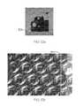
- FIG. 10shows the edge effect for a laser cut at 1360 ⁇ m (twice the center to center distance).
- FIG. 11shows the edge effect for a laser cut at 2040 ⁇ m (three times the center to center distance).
- FIG. 12shows the edge effect for a laser cut at 2720 ⁇ m (four times the center to center distance).
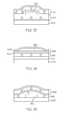
- FIG. 13is a cross-section of one embodiment of an environmentally sensitive device encapsulated by three dimensional multilayer barriers.
- FIG. 14is a cross-section of one embodiment of a three dimensional multilayer barrier and an edge sealed two dimensional barrier.
- FIG. 15is a cross-section of another embodiment of an environmentally sensitive device encapsulated by a three dimensional multilayer barrier.
- FIG. 2illustrates the concept of the three dimensional multilayer barrier 150 .
- the decoupling layers 160have sections 165 separated by walls 170 .
- the walls 170are made of barrier material.
- Dotted line 175indicates where a cut could be made that would still result in a wall between the cut edge and the defect 180 in the barrier layer which would prevent the permeants from diffusing to the environmentally sensitive device 185 , causing device failure.
- the wallscan be repeated as often as needed across the decoupling layer so that the three dimensional multilayer barrier can be cut while still providing a wall between the permeants and the device.
- the three dimensional multilayer barrier shown FIG. 2is highly simplistic. It depicts simple rectangular cross-sections and perfect staking of cellular decoupling layers.
- the cellscan be polygonal, circular, or other shapes, if desired.
- the wallsdo not have to be vertical or have the same thickness; however, they should have sufficient thickness at the thinnest point to provide effective barrier performance.
- the sections of the decoupling layerscan be offset from one another, if desired.
- the three dimensional multilayer barrier shown in FIG. 2can be made using a vacuum process.
- a planar barrier layercan be deposited by reactive sputtering.
- the discontinuous decoupling layerscan be deposited in a checkerboard pattern through masks with an intervening barrier layer deposition step.
- a barrier layeris deposited over the second decoupling layer. This process produces a cellular decoupling layer and barrier layer as shown in FIGS. 3 and 4 .
- the sections 210 of the second discontinuous decoupling layerare offset horizontally and vertically from, and are positioned between, the sections 205 of the first discontinuous decoupling layer.
- This processrequires 4 steps (not counting the initial barrier layer deposition) to make a decoupling layer/barrier layer pair in contrast to the two step process currently used (depositing a planar decoupling layer and a planar barrier layer). It also requires a high level of precision mask registration.
- the resulting structurehas vertical walls that are continuous through the thickness of the multilayer structure. This arrangement is undesirable for flexibility, which is an important characteristic of a barrier on a flexible substrate.
- the sections 220 of the fourth discontinuous decoupling layerare offset horizontally and vertically from, and are positioned between, the sections 215 of the third decoupling layer.
- the sections 215 of the third discontinuous decoupling layer and 220 of the fourth discontinuous decoupling layerare offset horizontally from the sections 205 of the first discontinuous decoupling layer and 210 of the second discontinuous decoupling layer.
- This structureis characterized by barrier materials forming small vertical “posts” 225 that are continuous through the thickness of the multilayer structure.
- a third decoupling layer/barrier layer pairmade by shifting the mask position (e.g., 1 ⁇ 4 cell width in both the x and y directions) will result in a structure having 3 decoupling layer/barrier layer pairs free of barrier material based structures that are continuous through the thickness.
- FIG. 7shows diagrams of the cross-section and planar views of circular and substantially square shapes.
- the cross-sectiontends to be semicircular in response to surface tension.
- the fluidWith a larger area, the fluid will tend to flatten in response to thickness creating a hydrostatic pressure that overcomes surface tension causing a flattening lateral flow.
- a two step vacuum processcould be used to make the three dimensional multilayer barrier.
- the barrier layerscan be deposited by reactive sputtering, with alternating patterned discontinuous decoupling layers deposited through masks.
- a possible cross-section of the resulting barrier structureis shown in FIG. 8 . Offsetting the masks between the decoupling layer/barrier layer pairs results in an overlapping pattern.
- barrier layersincluding, but not limited to, sputtering, reactive sputtering, chemical vapor deposition, plasma enhanced chemical vapor deposition, evaporation, sublimation, electron cyclotron resonance-plasma enhanced vapor deposition (ECR-PECVD), and combinations thereof.
- Barrier layersmay be made from materials including, but not limited to, metals, metal oxides, metal nitrides, metal carbides, metal oxynitrides, metal oxyborides, and combinations thereof.
- Metalsinclude, but are not limited to, aluminum, titanium, indium, tin, tantalum, zirconium, niobium, hafnium, yttrium, nickel, tungsten, chromium, zinc, alloys thereof, and combinations thereof.
- Metal oxidesinclude, but are not limited to, silicon oxide, aluminum oxide, titanium oxide, indium oxide, tin oxide, indium tin oxide, tantalum oxide, zirconium oxide, niobium oxide, hafnium oxide, yttrium oxide, nickel oxide, tungsten oxide, chromium oxide, zinc oxide, and combinations thereof.
- Metal nitridesinclude, but are not limited to, aluminum nitride, silicon nitride, boron nitride, germanium nitride, chromium nitride, nickel nitride, and combinations thereof.
- Metal carbidesinclude, but are not limited to, boron carbide, tungsten carbide, silicon carbide, and combinations thereof.
- Metal oxynitridesinclude, but are not limited to, aluminum oxynitride, silicon oxynitride, boron oxynitride, and combinations thereof.
- Metal oxyboridesinclude, but are not limited to, zirconium oxyboride, titanium oxyboride, and combinations thereof.
- the barrier layerscan be graded composition barriers, if desired. Suitable graded composition barriers include, but are not limited to, those described in U.S. Pat. No. 7,015,640, which is incorporated herein by reference
- Substantially opaque barrier layerscan be made from opaque materials including, but not limited to, opaque metals, opaque polymers, opaque ceramics, opaque cermets, and combinations thereof.
- Opaque cermetsinclude, but are not limited to, zirconium nitride, titanium nitride, hafnium nitride, tantalum nitride, niobium nitride, tungsten disilicide, titanium diboride, zirconium diboride, and combinations thereof.
- the decoupling layerscan be deposited using vacuum processes, including but not limited to, flash evaporation with in situ polymerization under vacuum, or plasma deposition and polymerization.
- the decoupling layerscan be made using an atmospheric process.
- Suitable atmospheric processesinclude, but are not limited to, spin coating, ink jet printing, screen printing, spraying, or combinations thereof.
- Ink jet printingis advantageous because it is a non-contact process, which avoids damage and contamination caused by contact with the fragile barrier layers.
- itis capable of producing the required feature sizes, and it can achieve the necessary accuracy of registration over multiple deposition steps.
- the decoupling layercould be deposited initially as a continuous layer using a process including, but not limited to, spin coating.
- the decoupling layercould then be divided into sections by a process including, but not limited to, mask etching.
- the surface of the substratecould be masked prior to the spincoating or other deposition process.
- Decoupling layerscan be made from materials including, but not limited to, organic polymers, inorganic polymers, organometallic polymers, hybrid organic/inorganic polymer systems, and silicates.
- Organic polymersinclude, but are not limited to, (meth)acrylates, urethanes, polyamides, polyimides, polybutylenes, isobutylene isoprene, polyolefins, epoxies, parylene, benzocyclobutadiene, polynorbornenes, polyarylethers, polycarbonate, alkyds, polyaniline, ethylene vinyl acetate, and ethylene acrylic acid.
- Inorganic polymersinclude, but are not limited to, silicones, polyphosphazenes, polysilazane, polycarbosilane, polycarborane, carborane siloxanes, polysilanes, phosphonitriles, sulfur nitride polymers, and siloxanes.
- Organometallic polymersinclude, but are not limited to, organometallic polymers of main group metals, transition metals and lanthanide/actinide metals (for example, polymetallocenylenes such as polyferrocene and polyruthenocene).
- Hybrid organic/inorganic polymer systemsinclude, but are not limited to, organically modified silicates, ceramers, preceramic polymers, polyimide-silica hybrids, (meth)acrylate-silica hybrids, polydimethylsiloxane-silica hybrids.
- a three dimensional multilayer barriercomprised of an initial barrier layer of 400 ⁇ with 4 decoupling layer/barrier layer pairs (0.5 ⁇ m of acrylate polymer and 400 ⁇ of aluminum oxide) was formed over the calcium on a glass substrate.
- the mask used to form the decoupling layerhad 480 ⁇ m diameter holes with a 200 ⁇ m distance between the holes, resulting in a 680 ⁇ m distance from the center of one hole to the center of the next.
- Laser cuts 305were made outside the calcium region 310 on 2 opposing sides, as shown schematically in FIG. 9 .
- the cutswere made at distances of 1360 ⁇ m (twice the center to center distance), 2040 ⁇ m (three times the center to center distance), and 2720 ⁇ m (four times the center to center distance).
- the barrier degradationwas observed along the cut edges.
- the sampleswere subjected to a temperature of 60° C. and 90% relative humidity.
- the results from the calcium testindicate that these samples have an oxygen transmission rate (OTR) of less than 0.005 cc/m 2 /day at 23° C. and 0% relative humidity, and less than 0.005 cc/m 2 /day at 38° C. and 90% relative humidity.
- OTRoxygen transmission rate
- WVTRwater vapor transmission rate
- the barrier layerscould be deposited as continuous layers across the entire substrate. This will be the most common situation. However, the barrier layers could also be deposited over only a portion of the substrate using a mask, for example, in order to form an array of devices in which each device is individually encapsulated. In this case, the barrier layer should be deposited over at least two sections of the discontinuous decoupling layer so that at least one wall of barrier material will be formed separating the sections of the discontinuous decoupling layer.
- a continuous layerwill not have any intentionally formed gaps in coverage.
- a discontinuous layerwill have intentionally formed gaps in coverage.
- the three dimensional multilayer barrier of the present inventioncan be used to encapsulate environmentally sensitive devices without the need to edge seal the barrier structures, as well as being used as barriers on flexible substrates.
- the three dimensional multilayer barrier of the present inventioncan be included on either side or both sides of the environmentally sensitive device, as desired.
- a first three dimensional multilayer barrier 410could be formed on a substrate 405 .
- An environmentally sensitive device 415could then be placed adjacent to the first three dimensional multilayer barrier 410 .
- a second three dimensional multilayer barrier 420could then be placed adjacent to the environmentally sensitive device 415 on the side opposite the first three dimensional multilayer barrier 410 .
- the environmentally sensitive device 415would be encapsulated between the first and second three dimensional multilayer barriers 410 , 420 .
- a conventional two dimensional barriercould be combined with the three dimensional multilayer barrier.
- a three dimensional multilayer barrier 515 and a two dimensional barrier 520there could be a three dimensional barrier 515 and a two dimensional barrier 520 .
- the two dimensional barrier 520could have an edge seal in which two barrier layers 525 and 535 enclose and form a seal around a decoupling layer 530 positioned between them.
- one or more functional layerscould be deposited before and/or after depositing the three dimensional multilayer barrier, and/or the two dimensional barrier. There could be functional layers on either or both sides of the environmentally sensitive device.
- FIG. 14shows a functional layer 510 between the substrate 505 and the three dimensional multilayer barrier 515 .
- the functional layerscan include, but are not limited to, planarizing layers, barrier layers, hard coats, scratch resistant coatings, thermal coefficient of expansion (TCE) matching coatings, plasma protection layers, coatings which modify optical properties, such as anti-reflection, viewing angle limiting, etc., adhesion enhancement, and the like.
- a discontinuous decoupling layercould be deposited before the first continuous barrier layer is deposited, if desired. This could be useful in encapsulating environmentally sensitive devices which have continuous cathodes as the top layer, including, but not limited to, active matrix devices and backlights.
- an environmentally sensitive device 610is positioned on substrate 605 .
- a discontinuous decoupling layer 615is deposited before the three dimensional multilayer barrier 620 .
Landscapes
- Physics & Mathematics (AREA)
- Chemical & Material Sciences (AREA)
- Power Engineering (AREA)
- Engineering & Computer Science (AREA)
- Computer Hardware Design (AREA)
- Microelectronics & Electronic Packaging (AREA)
- General Physics & Mathematics (AREA)
- Condensed Matter Physics & Semiconductors (AREA)
- Chemical Kinetics & Catalysis (AREA)
- Electrochemistry (AREA)
- General Chemical & Material Sciences (AREA)
- Inorganic Chemistry (AREA)
- Optics & Photonics (AREA)
- Laminated Bodies (AREA)
- Electroluminescent Light Sources (AREA)
Abstract
Description
- This application is a continuation-in-part of U.S. application Ser. No. 11/068,356, filed Feb. 28, 2005, which is a Division of U.S. application Ser. No. 09/966,163, filed Sep. 28, 2001, now U.S. Pat. No. 6,866,901, which is a continuation-in-part of U.S. application Ser. No. 09/427,138, filed Oct. 25, 1999, now U.S. Pat. No. 6,522,067, all of which are incorporated herein by reference.
- Multilayer, thin film barrier composites having alternating layers of barrier material and polymer material are known. For example, U.S. Pat. No. 6,268,695, entitled “Environmental Barrier Material For Organic Light Emitting Device And Method Of Making,” issued Jul. 31, 2001; U.S. Pat. No. 6,522,067, entitled “Environmental Barrier Material For Organic Light Emitting Device And Method Of Making,” issued Feb. 18, 2003; and U.S. Pat. No. 6,570,325, entitled “Environmental Barrier Material For Organic Light Emitting Device And Method Of Making”, issued May 27, 2003, all of which are incorporated herein by reference, describe encapsulated organic light emitting devices (OLEDs). These multilayer, thin film barrier composites are typically formed by depositing alternating layers of barrier material and decoupling material, such as by vacuum deposition.
- Lateral diffusion into the exposed permeable decoupling layers of a multilayer barrier is an issue with respect to use of these structures for encapsulation. Current multilayer barriers are two dimensional structures: planar barrier layers separated by planar decoupling layers. As a result, they are subject to permeation in the plane of the decoupling layer. If the decoupling layers are deposited over the entire surface of the substrate, then the edges of the decoupling layers are exposed to oxygen, moisture, and other contaminants. This potentially allows the moisture, oxygen, or other contaminants to diffuse laterally into an encapsulated environmentally sensitive device from the edge of the composite, as shown in
FIG. 1 . The multilayer, thin film barrier composite100 includes asubstrate 105 and alternating layers of decouplingmaterial 110 andbarrier material 115. The scale ofFIG. 1 is greatly expanded in the vertical direction. The area of thesubstrate 105 will typically vary from a few square centimeters to several square meters. Thebarrier layers 115 are typically a few hundred Angstroms thick, while the decouplinglayers 110 are generally less than ten microns thick. The lateral diffusion rate of moisture and oxygen is finite, and this will eventually compromise the encapsulation. One way to reduce the problem of edge diffusion is to provide long edge diffusion paths. However, this decreases the area of the substrate which is usable for active environmentally sensitive devices. In addition, it only lessens the problem, but does not eliminate it. - Lateral diffusion is also an issue for the use of multilayer barriers on polymer films to create flexible substrates. Practical usage, either roll to roll or sheet based, will require sectioning, or cutting, to yield individual devices, an operation which leads to exposed edges.
- Several methods have been proposed to protect the exposed edges. One method involves depositing multilayer barriers as an array of individual areas using methods that form edge sealing structures. An alternative method involves emplacing an edge sealing structure for each individual device subsequent to sectioning. Although both methods can be made to work, the impact of the additional processing steps and inventory logistics has prevented commercialization.
- Therefore, there is a need for a multilayer barrier which provides protection against lateral diffusion, and for a method of making the multilayer barrier.
- The present invention meets that need by providing a three dimensional multilayer barrier comprising a first continuous barrier layer adjacent to a substrate; a first discontinuous decoupling layer adjacent to the first continuous barrier layer, the first discontinuous decoupling layer having at least two sections; and a second continuous barrier layer adjacent to the first discontinuous decoupling layer, the second continuous barrier layer forming a wall separating the sections of the first discontinuous decoupling layer. By adjacent, we mean next to, but not necessarily directly next to. There can be additional layers between two adjacent layers.
- Another aspect of the invention relates to a method of making the three dimensional multilayer barrier. The method involves depositing a first continuous barrier layer adjacent to a substrate; depositing a first discontinuous decoupling layer adjacent to the first continuous barrier layer, the first discontinuous decoupling layer having at least two sections; and depositing a second continuous barrier layer adjacent to the first discontinuous decoupling layer, the second continuous barrier layer forming a wall separating the sections of the first discontinuous decoupling layer.
FIG. 1 is a cross-section showing lateral diffusion in a prior art two dimensional multilayer barrier.FIG. 2 is a cross-section showing one embodiment of a three dimensional multilayer barrier of the present invention.FIG. 3 is a cross-section of one embodiment of a three dimensional multilayer barrier of the present invention.FIG. 4 is a plan view of the embodiment ofFIG. 3 .FIG. 5 is a cross-section of one embodiment of a three dimensional multilayer barrier of the present invention.FIG. 6 is a plan view of the embodiment ofFIG. 5 .FIG. 7 is a diagram of the cross-section and planar views of different shapes for the discontinuous decoupling layer of the present invention.FIG. 8 is a cross-section of one embodiment of the present invention.FIG. 9 is a schematic showing the laser cuts on the outside of the calcium patch.FIG. 10 shows the edge effect for a laser cut at 1360 μm (twice the center to center distance).FIG. 11 shows the edge effect for a laser cut at 2040 μm (three times the center to center distance).FIG. 12 shows the edge effect for a laser cut at 2720 μm (four times the center to center distance).FIG. 13 is a cross-section of one embodiment of an environmentally sensitive device encapsulated by three dimensional multilayer barriers.FIG. 14 is a cross-section of one embodiment of a three dimensional multilayer barrier and an edge sealed two dimensional barrier.FIG. 15 is a cross-section of another embodiment of an environmentally sensitive device encapsulated by a three dimensional multilayer barrier.FIG. 2 illustrates the concept of the threedimensional multilayer barrier 150. There arealternating barrier layers 155 and decouplinglayers 160. The decouplinglayers 160 havesections 165 separated bywalls 170. Thewalls 170 are made of barrier material. Dottedline 175 indicates where a cut could be made that would still result in a wall between the cut edge and thedefect 180 in the barrier layer which would prevent the permeants from diffusing to the environmentallysensitive device 185, causing device failure. The walls can be repeated as often as needed across the decoupling layer so that the three dimensional multilayer barrier can be cut while still providing a wall between the permeants and the device.- The three dimensional multilayer barrier shown
FIG. 2 is highly simplistic. It depicts simple rectangular cross-sections and perfect staking of cellular decoupling layers. The cells can be polygonal, circular, or other shapes, if desired. The walls do not have to be vertical or have the same thickness; however, they should have sufficient thickness at the thinnest point to provide effective barrier performance. In order to achieve a uniform surface of the resulting multilayer barrier structure, the sections of the decoupling layers can be offset from one another, if desired. - The three dimensional multilayer barrier shown in
FIG. 2 can be made using a vacuum process. A planar barrier layer can be deposited by reactive sputtering. The discontinuous decoupling layers can be deposited in a checkerboard pattern through masks with an intervening barrier layer deposition step. A barrier layer is deposited over the second decoupling layer. This process produces a cellular decoupling layer and barrier layer as shown inFIGS. 3 and 4 . Thesections 210 of the second discontinuous decoupling layer are offset horizontally and vertically from, and are positioned between, thesections 205 of the first discontinuous decoupling layer. This process requires 4 steps (not counting the initial barrier layer deposition) to make a decoupling layer/barrier layer pair in contrast to the two step process currently used (depositing a planar decoupling layer and a planar barrier layer). It also requires a high level of precision mask registration. The resulting structure has vertical walls that are continuous through the thickness of the multilayer structure. This arrangement is undesirable for flexibility, which is an important characteristic of a barrier on a flexible substrate. - One solution to this situation is to maintain the mask placement within the decoupling layer/barrier layer pair, but shift the relative placement between one decoupling layer/barrier layer pair and the next. For example, shifting mask positions by ½ cell width in both the x and y directions to deposit third and fourth patterned decoupling layers would produce the structure shown in
FIGS. 5 and 6 . Thesections 220 of the fourth discontinuous decoupling layer are offset horizontally and vertically from, and are positioned between, thesections 215 of the third decoupling layer. Thesections 215 of the third discontinuous decoupling layer and220 of the fourth discontinuous decoupling layer are offset horizontally from thesections 205 of the first discontinuous decoupling layer and210 of the second discontinuous decoupling layer. This structure is characterized by barrier materials forming small vertical “posts”225 that are continuous through the thickness of the multilayer structure. - The addition of a third decoupling layer/barrier layer pair made by shifting the mask position (e.g., ¼ cell width in both the x and y directions) will result in a structure having 3 decoupling layer/barrier layer pairs free of barrier material based structures that are continuous through the thickness.
- The actual geometry of the deposited decoupling layer will not be as regular as is depicted in the preceding figures.
FIG. 7 shows diagrams of the cross-section and planar views of circular and substantially square shapes. With small areas of deposited fluid (in the tens of microns range), the cross-section tends to be semicircular in response to surface tension. With a larger area, the fluid will tend to flatten in response to thickness creating a hydrostatic pressure that overcomes surface tension causing a flattening lateral flow. It would be desirable to have the major percentage of the discontinuous decoupling layer covered by the decoupling material. This favors the square rather than the circular mask opening or the use of overlapping printed drops to create the more nearly square cross-section when larger size decoupling layer units are to be deposited. - A two step vacuum process could be used to make the three dimensional multilayer barrier. The barrier layers can be deposited by reactive sputtering, with alternating patterned discontinuous decoupling layers deposited through masks. A possible cross-section of the resulting barrier structure is shown in
FIG. 8 . Offsetting the masks between the decoupling layer/barrier layer pairs results in an overlapping pattern. - Various vacuum processes can be used to deposit the barrier layers including, but not limited to, sputtering, reactive sputtering, chemical vapor deposition, plasma enhanced chemical vapor deposition, evaporation, sublimation, electron cyclotron resonance-plasma enhanced vapor deposition (ECR-PECVD), and combinations thereof.
- Barrier layers may be made from materials including, but not limited to, metals, metal oxides, metal nitrides, metal carbides, metal oxynitrides, metal oxyborides, and combinations thereof. Metals include, but are not limited to, aluminum, titanium, indium, tin, tantalum, zirconium, niobium, hafnium, yttrium, nickel, tungsten, chromium, zinc, alloys thereof, and combinations thereof. Metal oxides include, but are not limited to, silicon oxide, aluminum oxide, titanium oxide, indium oxide, tin oxide, indium tin oxide, tantalum oxide, zirconium oxide, niobium oxide, hafnium oxide, yttrium oxide, nickel oxide, tungsten oxide, chromium oxide, zinc oxide, and combinations thereof. Metal nitrides include, but are not limited to, aluminum nitride, silicon nitride, boron nitride, germanium nitride, chromium nitride, nickel nitride, and combinations thereof. Metal carbides include, but are not limited to, boron carbide, tungsten carbide, silicon carbide, and combinations thereof. Metal oxynitrides include, but are not limited to, aluminum oxynitride, silicon oxynitride, boron oxynitride, and combinations thereof. Metal oxyborides include, but are not limited to, zirconium oxyboride, titanium oxyboride, and combinations thereof.
- The barrier layers can be graded composition barriers, if desired. Suitable graded composition barriers include, but are not limited to, those described in U.S. Pat. No. 7,015,640, which is incorporated herein by reference
- Substantially opaque barrier layers can be made from opaque materials including, but not limited to, opaque metals, opaque polymers, opaque ceramics, opaque cermets, and combinations thereof. Opaque cermets include, but are not limited to, zirconium nitride, titanium nitride, hafnium nitride, tantalum nitride, niobium nitride, tungsten disilicide, titanium diboride, zirconium diboride, and combinations thereof.
- The decoupling layers can be deposited using vacuum processes, including but not limited to, flash evaporation with in situ polymerization under vacuum, or plasma deposition and polymerization.
- Alternatively, the decoupling layers can be made using an atmospheric process. Suitable atmospheric processes include, but are not limited to, spin coating, ink jet printing, screen printing, spraying, or combinations thereof. Ink jet printing is advantageous because it is a non-contact process, which avoids damage and contamination caused by contact with the fragile barrier layers. In addition, it is capable of producing the required feature sizes, and it can achieve the necessary accuracy of registration over multiple deposition steps.
- The decoupling layer could be deposited initially as a continuous layer using a process including, but not limited to, spin coating. The decoupling layer could then be divided into sections by a process including, but not limited to, mask etching. Alternatively, the surface of the substrate could be masked prior to the spincoating or other deposition process.
- Decoupling layers can be made from materials including, but not limited to, organic polymers, inorganic polymers, organometallic polymers, hybrid organic/inorganic polymer systems, and silicates. Organic polymers include, but are not limited to, (meth)acrylates, urethanes, polyamides, polyimides, polybutylenes, isobutylene isoprene, polyolefins, epoxies, parylene, benzocyclobutadiene, polynorbornenes, polyarylethers, polycarbonate, alkyds, polyaniline, ethylene vinyl acetate, and ethylene acrylic acid. Inorganic polymers include, but are not limited to, silicones, polyphosphazenes, polysilazane, polycarbosilane, polycarborane, carborane siloxanes, polysilanes, phosphonitriles, sulfur nitride polymers, and siloxanes. Organometallic polymers include, but are not limited to, organometallic polymers of main group metals, transition metals and lanthanide/actinide metals (for example, polymetallocenylenes such as polyferrocene and polyruthenocene). Hybrid organic/inorganic polymer systems include, but are not limited to, organically modified silicates, ceramers, preceramic polymers, polyimide-silica hybrids, (meth)acrylate-silica hybrids, polydimethylsiloxane-silica hybrids.
- Tests were performed to evaluate the three dimensional multilayer barrier of the present invention using the calcium test. The calcium test is described in Nisato et al., “Thin Film Encapsulation for OLEDs: Evaluation of Multi-layer Barriers using the Ca Test,” SID 03 Digest, 2003, p. 550-553, which is incorporated herein by reference.
- A three dimensional multilayer barrier comprised of an initial barrier layer of 400 Å with 4 decoupling layer/barrier layer pairs (0.5 μm of acrylate polymer and 400 Å of aluminum oxide) was formed over the calcium on a glass substrate. The mask used to form the decoupling layer had 480 μm diameter holes with a 200 μm distance between the holes, resulting in a 680 μm distance from the center of one hole to the center of the next.
Laser cuts 305 were made outside thecalcium region 310 on 2 opposing sides, as shown schematically inFIG. 9 . The cuts were made at distances of 1360 μm (twice the center to center distance), 2040 μm (three times the center to center distance), and 2720 μm (four times the center to center distance). The barrier degradation was observed along the cut edges. The samples were subjected to a temperature of 60° C. and 90% relative humidity.- No edge effect was seen for any of the samples after 96 hrs. After 633 hrs, an edge effect was seen for the samples cut at 1360 μm (twice the center to center distance), as shown in
FIG. 10 . A possible minimal edge effect was seen for the samples cut at 2040 μm (three times the center to center distance), as shown inFIG. 11 . No edge effect was seen for the samples cut at 2720 μm (four times the center to center distance), as shown inFIG. 12 . Although there were many defects in all the samples, these were not caused by the cuts, but by debris in the coating, or excessive handling, or some other reason. - The results from the calcium test indicate that these samples have an oxygen transmission rate (OTR) of less than 0.005 cc/m2/day at 23° C. and 0% relative humidity, and less than 0.005 cc/m2/day at 38° C. and 90% relative humidity. The results also indicate that the samples have a water vapor transmission rate (WVTR) of less than 0.005 gm/m2/day at 38° C. and 100% relative humidity. These values are well below the detection limits of current industrial instrumentation used for permeation measurements (Mocon OxTran 2/20L and Permatran) (measured according to ASTM F 1927-98 and ASTM F 1249-90, respectively).
- The barrier layers could be deposited as continuous layers across the entire substrate. This will be the most common situation. However, the barrier layers could also be deposited over only a portion of the substrate using a mask, for example, in order to form an array of devices in which each device is individually encapsulated. In this case, the barrier layer should be deposited over at least two sections of the discontinuous decoupling layer so that at least one wall of barrier material will be formed separating the sections of the discontinuous decoupling layer.
- A continuous layer will not have any intentionally formed gaps in coverage. A discontinuous layer will have intentionally formed gaps in coverage.
- The three dimensional multilayer barrier of the present invention can be used to encapsulate environmentally sensitive devices without the need to edge seal the barrier structures, as well as being used as barriers on flexible substrates. The three dimensional multilayer barrier of the present invention can be included on either side or both sides of the environmentally sensitive device, as desired. As shown in
FIG. 13 , a first threedimensional multilayer barrier 410 could be formed on asubstrate 405. An environmentallysensitive device 415 could then be placed adjacent to the first threedimensional multilayer barrier 410. A second threedimensional multilayer barrier 420 could then be placed adjacent to the environmentallysensitive device 415 on the side opposite the first threedimensional multilayer barrier 410. The environmentallysensitive device 415 would be encapsulated between the first and second threedimensional multilayer barriers - Optionally, a conventional two dimensional barrier could be combined with the three dimensional multilayer barrier. For example, as shown in
FIG. 14 , there could be a threedimensional multilayer barrier 515 and a twodimensional barrier 520. Alternatively, there could be a two dimensional barrier and a three dimensional multilayer barrier on top of that. The twodimensional barrier 520 could have an edge seal in which twobarrier layers decoupling layer 530 positioned between them. - If desired, one or more functional layers could be deposited before and/or after depositing the three dimensional multilayer barrier, and/or the two dimensional barrier. There could be functional layers on either or both sides of the environmentally sensitive device.
FIG. 14 shows afunctional layer 510 between thesubstrate 505 and the threedimensional multilayer barrier 515. The functional layers can include, but are not limited to, planarizing layers, barrier layers, hard coats, scratch resistant coatings, thermal coefficient of expansion (TCE) matching coatings, plasma protection layers, coatings which modify optical properties, such as anti-reflection, viewing angle limiting, etc., adhesion enhancement, and the like. - In addition, a discontinuous decoupling layer could be deposited before the first continuous barrier layer is deposited, if desired. This could be useful in encapsulating environmentally sensitive devices which have continuous cathodes as the top layer, including, but not limited to, active matrix devices and backlights. As shown in
FIG. 15 , an environmentallysensitive device 610 is positioned onsubstrate 605. Adiscontinuous decoupling layer 615 is deposited before the threedimensional multilayer barrier 620. - While certain representative embodiments and details have been shown for purposes of illustrating the invention, it will be apparent to those skilled in the art that various changes in the compositions and methods disclosed herein may be made without departing from the scope of the invention, which is defined in the appended claims.
Claims (31)
Priority Applications (3)
| Application Number | Priority Date | Filing Date | Title |
|---|---|---|---|
| US11/627,583US20070196682A1 (en) | 1999-10-25 | 2007-01-26 | Three dimensional multilayer barrier and method of making |
| PCT/US2007/086591WO2008094352A1 (en) | 2007-01-26 | 2007-12-06 | Three dimensional multilayer barrier and method of making |
| TW097101210ATW200845314A (en) | 2007-01-26 | 2008-01-11 | Three dimensional multilayer barrier and method of making |
Applications Claiming Priority (4)
| Application Number | Priority Date | Filing Date | Title |
|---|---|---|---|
| US09/427,138US6522067B1 (en) | 1998-12-16 | 1999-10-25 | Environmental barrier material for organic light emitting device and method of making |
| US09/966,163US6866901B2 (en) | 1999-10-25 | 2001-09-28 | Method for edge sealing barrier films |
| US11/068,356US20050176181A1 (en) | 1999-10-25 | 2005-02-28 | Method for edge sealing barrier films |
| US11/627,583US20070196682A1 (en) | 1999-10-25 | 2007-01-26 | Three dimensional multilayer barrier and method of making |
Related Parent Applications (1)
| Application Number | Title | Priority Date | Filing Date |
|---|---|---|---|
| US11/068,356Continuation-In-PartUS20050176181A1 (en) | 1999-10-25 | 2005-02-28 | Method for edge sealing barrier films |
Publications (1)
| Publication Number | Publication Date |
|---|---|
| US20070196682A1true US20070196682A1 (en) | 2007-08-23 |
Family
ID=39456337
Family Applications (1)
| Application Number | Title | Priority Date | Filing Date |
|---|---|---|---|
| US11/627,583AbandonedUS20070196682A1 (en) | 1999-10-25 | 2007-01-26 | Three dimensional multilayer barrier and method of making |
Country Status (3)
| Country | Link |
|---|---|
| US (1) | US20070196682A1 (en) |
| TW (1) | TW200845314A (en) |
| WO (1) | WO2008094352A1 (en) |
Cited By (51)
| Publication number | Priority date | Publication date | Assignee | Title |
|---|---|---|---|---|
| US7420208B2 (en) | 2001-06-20 | 2008-09-02 | Semiconductor Energy Laboratory Co., Ltd. | Light emitting device and method of manufacturing the same |
| WO2008142645A1 (en)* | 2007-05-24 | 2008-11-27 | Koninklijke Philips Electronics N.V. | Encapsulation for an electronic thin film device |
| US20080305360A1 (en)* | 2007-06-05 | 2008-12-11 | Dong-Won Han | Organic light emitting device and method of manufacturing the same |
| US20100031997A1 (en)* | 2008-08-11 | 2010-02-11 | Basol Bulent M | Flexible thin film photovoltaic modules and manufacturing the same |
| US7675074B2 (en) | 2002-05-15 | 2010-03-09 | Semiconductor Energy Laboratory Co., Ltd. | Light emitting device including a lamination layer |
| US7728326B2 (en) | 2001-06-20 | 2010-06-01 | Semiconductor Energy Laboratory Co., Ltd. | Light emitting device and electronic apparatus |
| US20100151209A1 (en)* | 2008-12-15 | 2010-06-17 | Industrial Technology Research Institute | Organic/inorganic multi-layered gas barrier film |
| US20110062603A1 (en)* | 2009-05-08 | 2011-03-17 | Hawker Craig J | Encapsulation architectures for utilizing flexible barrier films |
| US7959769B2 (en) | 2004-12-08 | 2011-06-14 | Infinite Power Solutions, Inc. | Deposition of LiCoO2 |
| US20110162705A1 (en)* | 2010-01-06 | 2011-07-07 | Popa Paul J | Moisture resistant photovoltaic devices with elastomeric, polysiloxane protection layer |
| EP2346108A1 (en) | 2010-01-15 | 2011-07-20 | Nederlandse Organisatie voor toegepast -natuurwetenschappelijk onderzoek TNO | Foil shaped electro-optical product, semi-finished product and method and apparatus for manufacturing the same |
| US7993773B2 (en) | 2002-08-09 | 2011-08-09 | Infinite Power Solutions, Inc. | Electrochemical apparatus with barrier layer protected substrate |
| WO2011097634A1 (en) | 2010-02-08 | 2011-08-11 | On Demand Therapeutics, Inc. | Low-permeability, laser-activated drug delivery device |
| US20110198620A1 (en)* | 2009-12-31 | 2011-08-18 | Samsung Mobile Display Co., Ltd. | Barrier film composite and display apparatus including the barrier film composite |
| US20110210344A1 (en)* | 2009-12-31 | 2011-09-01 | Samsung Mobile Display Co., Ltd. | Barrier film composite, display apparatus including the barrier film composite, and method of manufacturing display apparatus including the barrier film composite |
| US20110212304A1 (en)* | 2009-12-31 | 2011-09-01 | Samsung Mobile Display Co., Ltd. | Barrier film composite, display apparatus including the barrier film composite, method of manufacturing barrier film composite, and method of manufacturing display apparatus including the barrier film composite |
| US8021778B2 (en) | 2002-08-09 | 2011-09-20 | Infinite Power Solutions, Inc. | Electrochemical apparatus with barrier layer protected substrate |
| US8062708B2 (en) | 2006-09-29 | 2011-11-22 | Infinite Power Solutions, Inc. | Masking of and material constraint for depositing battery layers on flexible substrates |
| US8197781B2 (en) | 2006-11-07 | 2012-06-12 | Infinite Power Solutions, Inc. | Sputtering target of Li3PO4 and method for producing same |
| US8236443B2 (en) | 2002-08-09 | 2012-08-07 | Infinite Power Solutions, Inc. | Metal film encapsulation |
| US8260203B2 (en) | 2008-09-12 | 2012-09-04 | Infinite Power Solutions, Inc. | Energy device with integral conductive surface for data communication via electromagnetic energy and method thereof |
| US8268488B2 (en) | 2007-12-21 | 2012-09-18 | Infinite Power Solutions, Inc. | Thin film electrolyte for thin film batteries |
| US8350519B2 (en) | 2008-04-02 | 2013-01-08 | Infinite Power Solutions, Inc | Passive over/under voltage control and protection for energy storage devices associated with energy harvesting |
| US8394522B2 (en) | 2002-08-09 | 2013-03-12 | Infinite Power Solutions, Inc. | Robust metal film encapsulation |
| US8404376B2 (en) | 2002-08-09 | 2013-03-26 | Infinite Power Solutions, Inc. | Metal film encapsulation |
| CN103022354A (en)* | 2012-12-28 | 2013-04-03 | 昆山工研院新型平板显示技术中心有限公司 | Flexible substrate |
| US8431264B2 (en) | 2002-08-09 | 2013-04-30 | Infinite Power Solutions, Inc. | Hybrid thin-film battery |
| US8445130B2 (en) | 2002-08-09 | 2013-05-21 | Infinite Power Solutions, Inc. | Hybrid thin-film battery |
| US8508193B2 (en) | 2008-10-08 | 2013-08-13 | Infinite Power Solutions, Inc. | Environmentally-powered wireless sensor module |
| US8518581B2 (en) | 2008-01-11 | 2013-08-27 | Inifinite Power Solutions, Inc. | Thin film encapsulation for thin film batteries and other devices |
| US8599572B2 (en) | 2009-09-01 | 2013-12-03 | Infinite Power Solutions, Inc. | Printed circuit board with integrated thin film battery |
| EP2685515A1 (en)* | 2012-07-12 | 2014-01-15 | Nederlandse Organisatie voor toegepast -natuurwetenschappelijk onderzoek TNO | Method and system for dividing a barrier foil |
| US8636876B2 (en) | 2004-12-08 | 2014-01-28 | R. Ernest Demaray | Deposition of LiCoO2 |
| US8728285B2 (en) | 2003-05-23 | 2014-05-20 | Demaray, Llc | Transparent conductive oxides |
| US20140197427A1 (en)* | 2013-01-11 | 2014-07-17 | Samsung Display Co., Ltd | A display apparatus substrate having a plurality of organic and inorganic layers stacked |
| US8906523B2 (en) | 2008-08-11 | 2014-12-09 | Infinite Power Solutions, Inc. | Energy device with integral collector surface for electromagnetic energy harvesting and method thereof |
| US8937394B2 (en) | 2012-08-24 | 2015-01-20 | Industrial Technology Research Institute | Compound barrier layer, method for forming the same and package structure using the same |
| KR20150036525A (en)* | 2012-09-04 | 2015-04-07 | 샤프 가부시키가이샤 | Organic electroluminescent display, and production method therefor |
| EP2863446A3 (en)* | 2013-10-15 | 2015-05-13 | Samsung Display Co., Ltd. | Flexible organic light emitting diode display and manufacturing method thereof |
| US9142797B2 (en) | 2010-05-31 | 2015-09-22 | Industrial Technology Research Institute | Gas barrier substrate and organic electro-luminescent device |
| US9334557B2 (en) | 2007-12-21 | 2016-05-10 | Sapurast Research Llc | Method for sputter targets for electrolyte films |
| US9594287B2 (en)* | 2014-08-24 | 2017-03-14 | Royole Corporation | Substrate-less flexible display and method of manufacturing the same |
| US9634296B2 (en) | 2002-08-09 | 2017-04-25 | Sapurast Research Llc | Thin film battery on an integrated circuit or circuit board and method thereof |
| JP2017168348A (en)* | 2016-03-17 | 2017-09-21 | 株式会社ジャパンディスプレイ | Display device |
| WO2019232905A1 (en)* | 2018-06-08 | 2019-12-12 | 汉能新材料科技有限公司 | Device for thin film encapsulation and solar cell |
| US10680277B2 (en) | 2010-06-07 | 2020-06-09 | Sapurast Research Llc | Rechargeable, high-density electrochemical device |
| CN111384223A (en)* | 2018-12-29 | 2020-07-07 | Tcl集团股份有限公司 | Encapsulation film, encapsulation method of light emitting device, and light emitting apparatus |
| WO2021108278A1 (en)* | 2019-11-27 | 2021-06-03 | Applied Materials, Inc. | Encapsulation having polymer and dielectric layers for electronic display |
| WO2021108277A3 (en)* | 2019-11-27 | 2021-07-08 | Applied Materials, Inc. | Stretchable polymer and dielectric layers for electronic displays |
| WO2021108325A3 (en)* | 2019-11-27 | 2021-07-15 | Applied Materials, Inc. | Method of forming stretchable encapsulation for electronic displays |
| US20210359267A1 (en)* | 2018-11-01 | 2021-11-18 | Boe Technology Group Co., Ltd. | Display panel, manufacturing method thereof, and display apparatus |
Families Citing this family (3)
| Publication number | Priority date | Publication date | Assignee | Title |
|---|---|---|---|---|
| US9368749B2 (en) | 2013-03-12 | 2016-06-14 | Samsung Sdi Co., Ltd. | Patterned multilayered stack, and system and method for making the same |
| KR102271586B1 (en)* | 2013-10-15 | 2021-07-02 | 삼성디스플레이 주식회사 | Flexible organic light emitting device and method of menufacturing the same |
| FR3012345B1 (en) | 2013-10-29 | 2017-07-28 | Commissariat Energie Atomique | DEVICE FOR ENCAPSULATING A SENSITIVE DEVICE AND METHOD OF MAKING SAID DEVICE |
Citations (90)
| Publication number | Priority date | Publication date | Assignee | Title |
|---|---|---|---|---|
| US3941630A (en)* | 1974-04-29 | 1976-03-02 | Rca Corporation | Method of fabricating a charged couple radiation sensing device |
| US4266223A (en)* | 1978-12-08 | 1981-05-05 | W. H. Brady Co. | Thin panel display |
| US4313254A (en)* | 1979-10-30 | 1982-02-02 | The Johns Hopkins University | Thin-film silicon solar cell with metal boride bottom electrode |
| US4426275A (en)* | 1981-11-27 | 1984-01-17 | Deposition Technology, Inc. | Sputtering device adaptable for coating heat-sensitive substrates |
| US4572845A (en)* | 1983-07-05 | 1986-02-25 | Draiswerke Gmbh | Process for gluing wood chips and the like with liquid glue and apparatus for performing the process |
| US4581337A (en)* | 1983-07-07 | 1986-04-08 | E. I. Du Pont De Nemours And Company | Polyether polyamines as linking agents for particle reagents useful in immunoassays |
| US4722515A (en)* | 1984-11-06 | 1988-02-02 | Spectrum Control, Inc. | Atomizing device for vaporization |
| US4913090A (en)* | 1987-10-02 | 1990-04-03 | Mitsubishi Denki Kabushiki Kaisha | Chemical vapor deposition apparatus having cooling heads adjacent to gas dispersing heads in a single chamber |
| US5189405A (en)* | 1989-01-26 | 1993-02-23 | Sharp Kabushiki Kaisha | Thin film electroluminescent panel |
| US5203898A (en)* | 1991-12-16 | 1993-04-20 | Corning Incorporated | Method of making fluorine/boron doped silica tubes |
| US5204314A (en)* | 1990-07-06 | 1993-04-20 | Advanced Technology Materials, Inc. | Method for delivering an involatile reagent in vapor form to a CVD reactor |
| US5393607A (en)* | 1992-01-13 | 1995-02-28 | Mitsui Toatsu Chemiclas, Inc. | Laminated transparent plastic material and polymerizable monomer |
| US5395644A (en)* | 1992-08-21 | 1995-03-07 | Battelle Memorial Institute | Vacuum deposition and curing of liquid monomers |
| US5402314A (en)* | 1992-02-10 | 1995-03-28 | Sony Corporation | Printed circuit board having through-hole stopped with photo-curable solder resist |
| US5510173A (en)* | 1993-08-20 | 1996-04-23 | Southwall Technologies Inc. | Multiple layer thin films with improved corrosion resistance |
| US5512320A (en)* | 1993-01-28 | 1996-04-30 | Applied Materials, Inc. | Vacuum processing apparatus having improved throughput |
| US5607789A (en)* | 1995-01-23 | 1997-03-04 | Duracell Inc. | Light transparent multilayer moisture barrier for electrochemical cell tester and cell employing same |
| US5620524A (en)* | 1995-02-27 | 1997-04-15 | Fan; Chiko | Apparatus for fluid delivery in chemical vapor deposition systems |
| US5629389A (en)* | 1995-06-06 | 1997-05-13 | Hewlett-Packard Company | Polymer-based electroluminescent device with improved stability |
| US5711816A (en)* | 1990-07-06 | 1998-01-27 | Advanced Technolgy Materials, Inc. | Source reagent liquid delivery apparatus, and chemical vapor deposition system comprising same |
| US5725909A (en)* | 1993-10-04 | 1998-03-10 | Catalina Coatings, Inc. | Acrylate composite barrier coating process |
| US5731661A (en)* | 1996-07-15 | 1998-03-24 | Motorola, Inc. | Passivation of electroluminescent organic devices |
| US5736207A (en)* | 1994-10-27 | 1998-04-07 | Schott Glaswerke | Vessel of plastic having a barrier coating and a method of producing the vessel |
| US5747182A (en)* | 1992-07-27 | 1998-05-05 | Cambridge Display Technology Limited | Manufacture of electroluminescent devices |
| US5757126A (en)* | 1995-11-30 | 1998-05-26 | Motorola, Inc. | Passivated organic device having alternating layers of polymer and dielectric |
| US5869791A (en)* | 1995-04-18 | 1999-02-09 | U.S. Philips Corporation | Method and apparatus for a touch sensing device having a thin film insulation layer about the periphery of each sensing element |
| US5872355A (en)* | 1997-04-09 | 1999-02-16 | Hewlett-Packard Company | Electroluminescent device and fabrication method for a light detection system |
| US5891554A (en)* | 1994-02-25 | 1999-04-06 | Idemitsu Kosan Co., Ltd. | Organic electroluminescence device |
| US5895228A (en)* | 1996-11-14 | 1999-04-20 | International Business Machines Corporation | Encapsulation of organic light emitting devices using Siloxane or Siloxane derivatives |
| US5902641A (en)* | 1997-09-29 | 1999-05-11 | Battelle Memorial Institute | Flash evaporation of liquid monomer particle mixture |
| US5902688A (en)* | 1996-07-16 | 1999-05-11 | Hewlett-Packard Company | Electroluminescent display device |
| US5904958A (en)* | 1998-03-20 | 1999-05-18 | Rexam Industries Corp. | Adjustable nozzle for evaporation or organic monomers |
| US6013337A (en)* | 1996-01-30 | 2000-01-11 | Becton Dickinson And Company | Blood collection tube assembly |
| US6040017A (en)* | 1998-10-02 | 2000-03-21 | Sigma Laboratories, Inc. | Formation of multilayered photonic polymer composites |
| US6045864A (en)* | 1997-12-01 | 2000-04-04 | 3M Innovative Properties Company | Vapor coating method |
| US6066826A (en)* | 1998-03-16 | 2000-05-23 | Yializis; Angelo | Apparatus for plasma treatment of moving webs |
| US6178082B1 (en)* | 1998-02-26 | 2001-01-23 | International Business Machines Corporation | High temperature, conductive thin film diffusion barrier for ceramic/metal systems |
| US6195142B1 (en)* | 1995-12-28 | 2001-02-27 | Matsushita Electrical Industrial Company, Ltd. | Organic electroluminescence element, its manufacturing method, and display device using organic electroluminescence element |
| US6198217B1 (en)* | 1997-05-12 | 2001-03-06 | Matsushita Electric Industrial Co., Ltd. | Organic electroluminescent device having a protective covering comprising organic and inorganic layers |
| US6198220B1 (en)* | 1997-07-11 | 2001-03-06 | Emagin Corporation | Sealing structure for organic light emitting devices |
| US6203898B1 (en)* | 1997-08-29 | 2001-03-20 | 3M Innovatave Properties Company | Article comprising a substrate having a silicone coating |
| US6207238B1 (en)* | 1998-12-16 | 2001-03-27 | Battelle Memorial Institute | Plasma enhanced chemical deposition for high and/or low index of refraction polymers |
| US6207239B1 (en)* | 1998-12-16 | 2001-03-27 | Battelle Memorial Institute | Plasma enhanced chemical deposition of conjugated polymer |
| US6214422B1 (en)* | 1994-11-04 | 2001-04-10 | Sigma Laboratories Of Arizona, Inc. | Method of forming a hybrid polymer film |
| US6217947B1 (en)* | 1998-12-16 | 2001-04-17 | Battelle Memorial Institute | Plasma enhanced polymer deposition onto fixtures |
| US6224948B1 (en)* | 1997-09-29 | 2001-05-01 | Battelle Memorial Institute | Plasma enhanced chemical deposition with low vapor pressure compounds |
| US6228436B1 (en)* | 1998-12-16 | 2001-05-08 | Battelle Memorial Institute | Method of making light emitting polymer composite material |
| US6228434B1 (en)* | 1998-12-16 | 2001-05-08 | Battelle Memorial Institute | Method of making a conformal coating of a microtextured surface |
| US20020022156A1 (en)* | 1998-11-02 | 2002-02-21 | 3M Innovative Properties Company | Transparent conductive oxides for plastic flat panel displays |
| US6350034B1 (en)* | 1999-02-26 | 2002-02-26 | 3M Innovative Properties Company | Retroreflective articles having polymer multilayer reflective coatings |
| US20020025444A1 (en)* | 1998-01-13 | 2002-02-28 | 3M Innovative Properties Company | Multilayered polymer films with recyclable or recycled layers |
| US6352777B1 (en)* | 1998-08-19 | 2002-03-05 | The Trustees Of Princeton University | Organic photosensitive optoelectronic devices with transparent electrodes |
| US6358570B1 (en)* | 1999-03-31 | 2002-03-19 | Battelle Memorial Institute | Vacuum deposition and curing of oligomers and resins |
| US6361885B1 (en)* | 1998-04-10 | 2002-03-26 | Organic Display Technology | Organic electroluminescent materials and device made from such materials |
| US6512561B1 (en)* | 1997-08-29 | 2003-01-28 | Sharp Kabushiki Kaisha | Liquid crystal display with at least one phase compensation element |
| US6522067B1 (en)* | 1998-12-16 | 2003-02-18 | Battelle Memorial Institute | Environmental barrier material for organic light emitting device and method of making |
| US20030038590A1 (en)* | 2001-08-21 | 2003-02-27 | Silvernail Jeffrey Alan | Patterned oxygen and moisture absorber for organic optoelectronic device structures |
| US20030045021A1 (en)* | 2001-08-30 | 2003-03-06 | Tomonori Akai | Production method for organic electroluminescent device |
| US6537688B2 (en)* | 2000-12-01 | 2003-03-25 | Universal Display Corporation | Adhesive sealed organic optoelectronic structures |
| US6548912B1 (en)* | 1999-10-25 | 2003-04-15 | Battelle Memorial Institute | Semicoductor passivation using barrier coatings |
| US6681716B2 (en)* | 2001-11-27 | 2004-01-27 | General Electric Company | Apparatus and method for depositing large area coatings on non-planar surfaces |
| US20040018305A1 (en)* | 2002-04-15 | 2004-01-29 | Pagano John Chris | Apparatus for depositing a multilayer coating on discrete sheets |
| US20040029334A1 (en)* | 2002-05-21 | 2004-02-12 | Otb Group B.V. | Method for passivating a semiconductor substrate |
| US20040046497A1 (en)* | 2002-09-11 | 2004-03-11 | General Electric Company | Diffusion barrier coatings having graded compositions and devices incorporating the same |
| US6720203B2 (en)* | 1999-04-28 | 2004-04-13 | E. I. Du Pont De Nemours And Company | Flexible organic electronic device with improved resistance to oxygen and moisture degradation |
| US20040071971A1 (en)* | 2002-10-11 | 2004-04-15 | General Electric Company | Bond layer for coatings on plastic substrates |
| US6837950B1 (en)* | 1998-11-05 | 2005-01-04 | Interface, Inc. | Separation of floor covering components for recycling |
| US20050006786A1 (en)* | 2002-03-01 | 2005-01-13 | Kabushiki Kaisha Toshiba | Semiconductor device and method of fabricating the same |
| US6864629B2 (en)* | 1999-01-29 | 2005-03-08 | Pioneer Corporation | Organic electroluminescence (EL) cell that prevents moisture from deteriorating light-emitting characteristics and a method for producing the same |
| US20050051094A1 (en)* | 2003-09-05 | 2005-03-10 | Mark Schaepkens | Replaceable plate expanded thermal plasma apparatus and method |
| US6866901B2 (en)* | 1999-10-25 | 2005-03-15 | Vitex Systems, Inc. | Method for edge sealing barrier films |
| US6867539B1 (en)* | 2000-07-12 | 2005-03-15 | 3M Innovative Properties Company | Encapsulated organic electronic devices and method for making same |
| US6872114B2 (en)* | 2001-10-17 | 2005-03-29 | Chi Mei Optolectronics Corporation | Method of sealing organo electro-luminescent display |
| US6872248B2 (en)* | 2002-03-29 | 2005-03-29 | Canon Kabushiki Kaisha | Liquid-phase growth process and liquid-phase growth apparatus |
| US6872428B2 (en)* | 2001-06-11 | 2005-03-29 | General Electric Company | Apparatus and method for large area chemical vapor deposition using multiple expanding thermal plasma generators |
| US6878467B2 (en)* | 2001-04-10 | 2005-04-12 | Chi Mei Optoelectronics Corporation | Organic electro-luminescence element used in a display device |
| US20050079295A1 (en)* | 2001-11-27 | 2005-04-14 | Marc Schaepkens | Apparatus and method for depositing large area coatings on planar surfaces |
| US20050079380A1 (en)* | 2003-09-30 | 2005-04-14 | Fuji Photo Film Co., Ltd. | Gas barrier laminate film and method for producing the same |
| US20060003474A1 (en)* | 2004-06-30 | 2006-01-05 | Eastman Kodak Company | Roll-to-sheet manufacture of OLED materials |
| US20060001040A1 (en)* | 2004-06-30 | 2006-01-05 | General Electric Company | High integrity protective coatings |
| US20060028128A1 (en)* | 2004-03-08 | 2006-02-09 | Fuji Photo Film Co., Ltd. | Display device |
| US6998648B2 (en)* | 2003-08-25 | 2006-02-14 | Universal Display Corporation | Protected organic electronic device structures incorporating pressure sensitive adhesive and desiccant |
| US7002294B2 (en)* | 2001-12-20 | 2006-02-21 | Universal Display Corporation | Method of protecting organic optoelectronic devices |
| US7012363B2 (en)* | 2002-01-10 | 2006-03-14 | Universal Display Corporation | OLEDs having increased external electroluminescence quantum efficiencies |
| US20060063015A1 (en)* | 2004-09-23 | 2006-03-23 | 3M Innovative Properties Company | Protected polymeric film |
| US20060062937A1 (en)* | 2003-04-02 | 2006-03-23 | 3M Innovative Properties Company | Flexible high-temperature ultrabarrier |
| US7029765B2 (en)* | 2003-04-22 | 2006-04-18 | Universal Display Corporation | Organic light emitting devices having reduced pixel shrinkage |
| US7156942B2 (en)* | 2002-12-19 | 2007-01-02 | 3M Innovative Properties Company | Organic electroluminescent device and encapsulation method |
| US20070009674A1 (en)* | 2003-05-29 | 2007-01-11 | Yasushi Okubo | Transparent film for display substrate, display substrate using the film and method of manufacturing the same, liquid crystal display, organic electroluminescence display, and touch panel |
| US7198832B2 (en)* | 1999-10-25 | 2007-04-03 | Vitex Systems, Inc. | Method for edge sealing barrier films |
Family Cites Families (1)
| Publication number | Priority date | Publication date | Assignee | Title |
|---|---|---|---|---|
| WO2004112165A1 (en)* | 2003-06-16 | 2004-12-23 | Koninklijke Philips Electronics N.V. | Barrier laminate for an electroluminescent device |
- 2007
- 2007-01-26USUS11/627,583patent/US20070196682A1/ennot_activeAbandoned
- 2007-12-06WOPCT/US2007/086591patent/WO2008094352A1/enactiveApplication Filing
- 2008
- 2008-01-11TWTW097101210Apatent/TW200845314A/enunknown
Patent Citations (99)
| Publication number | Priority date | Publication date | Assignee | Title |
|---|---|---|---|---|
| US3941630A (en)* | 1974-04-29 | 1976-03-02 | Rca Corporation | Method of fabricating a charged couple radiation sensing device |
| US4266223A (en)* | 1978-12-08 | 1981-05-05 | W. H. Brady Co. | Thin panel display |
| US4313254A (en)* | 1979-10-30 | 1982-02-02 | The Johns Hopkins University | Thin-film silicon solar cell with metal boride bottom electrode |
| US4426275A (en)* | 1981-11-27 | 1984-01-17 | Deposition Technology, Inc. | Sputtering device adaptable for coating heat-sensitive substrates |
| US4572845A (en)* | 1983-07-05 | 1986-02-25 | Draiswerke Gmbh | Process for gluing wood chips and the like with liquid glue and apparatus for performing the process |
| US4581337A (en)* | 1983-07-07 | 1986-04-08 | E. I. Du Pont De Nemours And Company | Polyether polyamines as linking agents for particle reagents useful in immunoassays |
| US4722515A (en)* | 1984-11-06 | 1988-02-02 | Spectrum Control, Inc. | Atomizing device for vaporization |
| US4913090A (en)* | 1987-10-02 | 1990-04-03 | Mitsubishi Denki Kabushiki Kaisha | Chemical vapor deposition apparatus having cooling heads adjacent to gas dispersing heads in a single chamber |
| US5189405A (en)* | 1989-01-26 | 1993-02-23 | Sharp Kabushiki Kaisha | Thin film electroluminescent panel |
| US5204314A (en)* | 1990-07-06 | 1993-04-20 | Advanced Technology Materials, Inc. | Method for delivering an involatile reagent in vapor form to a CVD reactor |
| US5711816A (en)* | 1990-07-06 | 1998-01-27 | Advanced Technolgy Materials, Inc. | Source reagent liquid delivery apparatus, and chemical vapor deposition system comprising same |
| US5203898A (en)* | 1991-12-16 | 1993-04-20 | Corning Incorporated | Method of making fluorine/boron doped silica tubes |
| US5393607A (en)* | 1992-01-13 | 1995-02-28 | Mitsui Toatsu Chemiclas, Inc. | Laminated transparent plastic material and polymerizable monomer |
| US5402314A (en)* | 1992-02-10 | 1995-03-28 | Sony Corporation | Printed circuit board having through-hole stopped with photo-curable solder resist |
| US5747182A (en)* | 1992-07-27 | 1998-05-05 | Cambridge Display Technology Limited | Manufacture of electroluminescent devices |
| US5395644A (en)* | 1992-08-21 | 1995-03-07 | Battelle Memorial Institute | Vacuum deposition and curing of liquid monomers |
| US5512320A (en)* | 1993-01-28 | 1996-04-30 | Applied Materials, Inc. | Vacuum processing apparatus having improved throughput |
| US5510173A (en)* | 1993-08-20 | 1996-04-23 | Southwall Technologies Inc. | Multiple layer thin films with improved corrosion resistance |
| US5725909A (en)* | 1993-10-04 | 1998-03-10 | Catalina Coatings, Inc. | Acrylate composite barrier coating process |
| US6231939B1 (en)* | 1993-10-04 | 2001-05-15 | Presstek, Inc. | Acrylate composite barrier coating |
| US5891554A (en)* | 1994-02-25 | 1999-04-06 | Idemitsu Kosan Co., Ltd. | Organic electroluminescence device |
| US5736207A (en)* | 1994-10-27 | 1998-04-07 | Schott Glaswerke | Vessel of plastic having a barrier coating and a method of producing the vessel |
| US6214422B1 (en)* | 1994-11-04 | 2001-04-10 | Sigma Laboratories Of Arizona, Inc. | Method of forming a hybrid polymer film |
| US5607789A (en)* | 1995-01-23 | 1997-03-04 | Duracell Inc. | Light transparent multilayer moisture barrier for electrochemical cell tester and cell employing same |
| US5620524A (en)* | 1995-02-27 | 1997-04-15 | Fan; Chiko | Apparatus for fluid delivery in chemical vapor deposition systems |
| US5869791A (en)* | 1995-04-18 | 1999-02-09 | U.S. Philips Corporation | Method and apparatus for a touch sensing device having a thin film insulation layer about the periphery of each sensing element |
| US5629389A (en)* | 1995-06-06 | 1997-05-13 | Hewlett-Packard Company | Polymer-based electroluminescent device with improved stability |
| US5757126A (en)* | 1995-11-30 | 1998-05-26 | Motorola, Inc. | Passivated organic device having alternating layers of polymer and dielectric |
| US6195142B1 (en)* | 1995-12-28 | 2001-02-27 | Matsushita Electrical Industrial Company, Ltd. | Organic electroluminescence element, its manufacturing method, and display device using organic electroluminescence element |
| US6013337A (en)* | 1996-01-30 | 2000-01-11 | Becton Dickinson And Company | Blood collection tube assembly |
| US5731661A (en)* | 1996-07-15 | 1998-03-24 | Motorola, Inc. | Passivation of electroluminescent organic devices |
| US5902688A (en)* | 1996-07-16 | 1999-05-11 | Hewlett-Packard Company | Electroluminescent display device |
| US5895228A (en)* | 1996-11-14 | 1999-04-20 | International Business Machines Corporation | Encapsulation of organic light emitting devices using Siloxane or Siloxane derivatives |
| US5872355A (en)* | 1997-04-09 | 1999-02-16 | Hewlett-Packard Company | Electroluminescent device and fabrication method for a light detection system |
| US6198217B1 (en)* | 1997-05-12 | 2001-03-06 | Matsushita Electric Industrial Co., Ltd. | Organic electroluminescent device having a protective covering comprising organic and inorganic layers |
| US6198220B1 (en)* | 1997-07-11 | 2001-03-06 | Emagin Corporation | Sealing structure for organic light emitting devices |
| US6348237B2 (en)* | 1997-08-29 | 2002-02-19 | 3M Innovative Properties Company | Jet plasma process for deposition of coatings |
| US6512561B1 (en)* | 1997-08-29 | 2003-01-28 | Sharp Kabushiki Kaisha | Liquid crystal display with at least one phase compensation element |
| US20050003098A1 (en)* | 1997-08-29 | 2005-01-06 | 3M Innovative Properties Company | Flash evaporation-plasma coating deposition method |
| US6203898B1 (en)* | 1997-08-29 | 2001-03-20 | 3M Innovatave Properties Company | Article comprising a substrate having a silicone coating |
| US6224948B1 (en)* | 1997-09-29 | 2001-05-01 | Battelle Memorial Institute | Plasma enhanced chemical deposition with low vapor pressure compounds |
| US5902641A (en)* | 1997-09-29 | 1999-05-11 | Battelle Memorial Institute | Flash evaporation of liquid monomer particle mixture |
| US6045864A (en)* | 1997-12-01 | 2000-04-04 | 3M Innovative Properties Company | Vapor coating method |
| US20020025444A1 (en)* | 1998-01-13 | 2002-02-28 | 3M Innovative Properties Company | Multilayered polymer films with recyclable or recycled layers |
| US6178082B1 (en)* | 1998-02-26 | 2001-01-23 | International Business Machines Corporation | High temperature, conductive thin film diffusion barrier for ceramic/metal systems |
| US6066826A (en)* | 1998-03-16 | 2000-05-23 | Yializis; Angelo | Apparatus for plasma treatment of moving webs |
| US5904958A (en)* | 1998-03-20 | 1999-05-18 | Rexam Industries Corp. | Adjustable nozzle for evaporation or organic monomers |
| US6361885B1 (en)* | 1998-04-10 | 2002-03-26 | Organic Display Technology | Organic electroluminescent materials and device made from such materials |
| US6352777B1 (en)* | 1998-08-19 | 2002-03-05 | The Trustees Of Princeton University | Organic photosensitive optoelectronic devices with transparent electrodes |
| US6040017A (en)* | 1998-10-02 | 2000-03-21 | Sigma Laboratories, Inc. | Formation of multilayered photonic polymer composites |
| US7186465B2 (en)* | 1998-11-02 | 2007-03-06 | 3M Innovative Properties Company | Transparent conductive oxides for plastic flat panel displays |
| US20020022156A1 (en)* | 1998-11-02 | 2002-02-21 | 3M Innovative Properties Company | Transparent conductive oxides for plastic flat panel displays |
| US6837950B1 (en)* | 1998-11-05 | 2005-01-04 | Interface, Inc. | Separation of floor covering components for recycling |
| US6217947B1 (en)* | 1998-12-16 | 2001-04-17 | Battelle Memorial Institute | Plasma enhanced polymer deposition onto fixtures |
| US6228434B1 (en)* | 1998-12-16 | 2001-05-08 | Battelle Memorial Institute | Method of making a conformal coating of a microtextured surface |
| US6509065B2 (en)* | 1998-12-16 | 2003-01-21 | Battelle Memorial Institute | Plasma enhanced chemical deposition of conjugated polymer |
| US6228436B1 (en)* | 1998-12-16 | 2001-05-08 | Battelle Memorial Institute | Method of making light emitting polymer composite material |
| US6522067B1 (en)* | 1998-12-16 | 2003-02-18 | Battelle Memorial Institute | Environmental barrier material for organic light emitting device and method of making |
| US6207238B1 (en)* | 1998-12-16 | 2001-03-27 | Battelle Memorial Institute | Plasma enhanced chemical deposition for high and/or low index of refraction polymers |
| US6207239B1 (en)* | 1998-12-16 | 2001-03-27 | Battelle Memorial Institute | Plasma enhanced chemical deposition of conjugated polymer |
| US6544600B2 (en)* | 1998-12-16 | 2003-04-08 | Battelle Memorial Institute | Plasma enhanced chemical deposition of conjugated polymer |
| US6864629B2 (en)* | 1999-01-29 | 2005-03-08 | Pioneer Corporation | Organic electroluminescence (EL) cell that prevents moisture from deteriorating light-emitting characteristics and a method for producing the same |
| US6350034B1 (en)* | 1999-02-26 | 2002-02-26 | 3M Innovative Properties Company | Retroreflective articles having polymer multilayer reflective coatings |
| US6358570B1 (en)* | 1999-03-31 | 2002-03-19 | Battelle Memorial Institute | Vacuum deposition and curing of oligomers and resins |
| US6720203B2 (en)* | 1999-04-28 | 2004-04-13 | E. I. Du Pont De Nemours And Company | Flexible organic electronic device with improved resistance to oxygen and moisture degradation |
| US7198832B2 (en)* | 1999-10-25 | 2007-04-03 | Vitex Systems, Inc. | Method for edge sealing barrier films |
| US6548912B1 (en)* | 1999-10-25 | 2003-04-15 | Battelle Memorial Institute | Semicoductor passivation using barrier coatings |
| US6866901B2 (en)* | 1999-10-25 | 2005-03-15 | Vitex Systems, Inc. | Method for edge sealing barrier films |
| US6867539B1 (en)* | 2000-07-12 | 2005-03-15 | 3M Innovative Properties Company | Encapsulated organic electronic devices and method for making same |
| US6537688B2 (en)* | 2000-12-01 | 2003-03-25 | Universal Display Corporation | Adhesive sealed organic optoelectronic structures |
| US6878467B2 (en)* | 2001-04-10 | 2005-04-12 | Chi Mei Optoelectronics Corporation | Organic electro-luminescence element used in a display device |
| US6872428B2 (en)* | 2001-06-11 | 2005-03-29 | General Electric Company | Apparatus and method for large area chemical vapor deposition using multiple expanding thermal plasma generators |
| US20030038590A1 (en)* | 2001-08-21 | 2003-02-27 | Silvernail Jeffrey Alan | Patterned oxygen and moisture absorber for organic optoelectronic device structures |
| US20030045021A1 (en)* | 2001-08-30 | 2003-03-06 | Tomonori Akai | Production method for organic electroluminescent device |
| US6872114B2 (en)* | 2001-10-17 | 2005-03-29 | Chi Mei Optolectronics Corporation | Method of sealing organo electro-luminescent display |
| US6681716B2 (en)* | 2001-11-27 | 2004-01-27 | General Electric Company | Apparatus and method for depositing large area coatings on non-planar surfaces |
| US20050079295A1 (en)* | 2001-11-27 | 2005-04-14 | Marc Schaepkens | Apparatus and method for depositing large area coatings on planar surfaces |
| US7002294B2 (en)* | 2001-12-20 | 2006-02-21 | Universal Display Corporation | Method of protecting organic optoelectronic devices |
| US7012363B2 (en)* | 2002-01-10 | 2006-03-14 | Universal Display Corporation | OLEDs having increased external electroluminescence quantum efficiencies |
| US20050006786A1 (en)* | 2002-03-01 | 2005-01-13 | Kabushiki Kaisha Toshiba | Semiconductor device and method of fabricating the same |
| US6872248B2 (en)* | 2002-03-29 | 2005-03-29 | Canon Kabushiki Kaisha | Liquid-phase growth process and liquid-phase growth apparatus |
| US20040018305A1 (en)* | 2002-04-15 | 2004-01-29 | Pagano John Chris | Apparatus for depositing a multilayer coating on discrete sheets |
| US20040029334A1 (en)* | 2002-05-21 | 2004-02-12 | Otb Group B.V. | Method for passivating a semiconductor substrate |
| US7015640B2 (en)* | 2002-09-11 | 2006-03-21 | General Electric Company | Diffusion barrier coatings having graded compositions and devices incorporating the same |
| US20040046497A1 (en)* | 2002-09-11 | 2004-03-11 | General Electric Company | Diffusion barrier coatings having graded compositions and devices incorporating the same |
| US20040071971A1 (en)* | 2002-10-11 | 2004-04-15 | General Electric Company | Bond layer for coatings on plastic substrates |
| US7156942B2 (en)* | 2002-12-19 | 2007-01-02 | 3M Innovative Properties Company | Organic electroluminescent device and encapsulation method |
| US20060062937A1 (en)* | 2003-04-02 | 2006-03-23 | 3M Innovative Properties Company | Flexible high-temperature ultrabarrier |
| US7018713B2 (en)* | 2003-04-02 | 2006-03-28 | 3M Innovative Properties Company | Flexible high-temperature ultrabarrier |
| US7029765B2 (en)* | 2003-04-22 | 2006-04-18 | Universal Display Corporation | Organic light emitting devices having reduced pixel shrinkage |
| US20070009674A1 (en)* | 2003-05-29 | 2007-01-11 | Yasushi Okubo | Transparent film for display substrate, display substrate using the film and method of manufacturing the same, liquid crystal display, organic electroluminescence display, and touch panel |
| US6998648B2 (en)* | 2003-08-25 | 2006-02-14 | Universal Display Corporation | Protected organic electronic device structures incorporating pressure sensitive adhesive and desiccant |
| US20050051094A1 (en)* | 2003-09-05 | 2005-03-10 | Mark Schaepkens | Replaceable plate expanded thermal plasma apparatus and method |
| US20050079380A1 (en)* | 2003-09-30 | 2005-04-14 | Fuji Photo Film Co., Ltd. | Gas barrier laminate film and method for producing the same |
| US20060028128A1 (en)* | 2004-03-08 | 2006-02-09 | Fuji Photo Film Co., Ltd. | Display device |
| US20060003474A1 (en)* | 2004-06-30 | 2006-01-05 | Eastman Kodak Company | Roll-to-sheet manufacture of OLED materials |
| US7033850B2 (en)* | 2004-06-30 | 2006-04-25 | Eastman Kodak Company | Roll-to-sheet manufacture of OLED materials |
| US20060001040A1 (en)* | 2004-06-30 | 2006-01-05 | General Electric Company | High integrity protective coatings |
| US20060063015A1 (en)* | 2004-09-23 | 2006-03-23 | 3M Innovative Properties Company | Protected polymeric film |
Cited By (107)
| Publication number | Priority date | Publication date | Assignee | Title |
|---|---|---|---|---|
| US7952101B2 (en) | 2001-06-20 | 2011-05-31 | Semiconductor Energy Laboratory Co., Ltd. | Light emitting device and method of manufacturing the same |
| US9166180B2 (en) | 2001-06-20 | 2015-10-20 | Semiconductor Energy Laboratory Co., Ltd. | Light emitting device having an organic light emitting diode that emits white light |
| US8415660B2 (en) | 2001-06-20 | 2013-04-09 | Semiconductor Energy Laboratory Co., Ltd. | Light emitting device |
| US20080303408A1 (en)* | 2001-06-20 | 2008-12-11 | Semiconductor Energy Laboratory Co., Ltd. | Light emitting device and method of manufacturing the same |
| US9178168B2 (en) | 2001-06-20 | 2015-11-03 | Semiconductor Energy Laboratory Co., Ltd. | White light emitting device |
| US9276224B2 (en) | 2001-06-20 | 2016-03-01 | Semiconductor Energy Laboratory Co., Ltd. | Organic light emitting device having dual flexible substrates |
| US7728326B2 (en) | 2001-06-20 | 2010-06-01 | Semiconductor Energy Laboratory Co., Ltd. | Light emitting device and electronic apparatus |
| US8134149B2 (en) | 2001-06-20 | 2012-03-13 | Semiconductor Energy Laboratory Co., Ltd. | Organic light emitting device |
| US7420208B2 (en) | 2001-06-20 | 2008-09-02 | Semiconductor Energy Laboratory Co., Ltd. | Light emitting device and method of manufacturing the same |
| US8822982B2 (en) | 2001-06-20 | 2014-09-02 | Semiconductor Energy Laboratory Co., Ltd. | Light emitting device and electronic apparatus |
| US20110233557A1 (en)* | 2001-06-20 | 2011-09-29 | Semiconductor Energy Laboratory Co., Ltd. | Light emitting device and method of manufacturing the same |
| US8659012B2 (en) | 2002-05-15 | 2014-02-25 | Semiconductor Energy Laboratory Co., Ltd. | Light emitting device |
| US20100156287A1 (en)* | 2002-05-15 | 2010-06-24 | Semiconductor Energy Laboratory Co., Ltd. | Light emitting device |
| US8129715B2 (en) | 2002-05-15 | 2012-03-06 | Semiconductor Energy Labratory Co., Ltd. | Light emitting device |
| US7675074B2 (en) | 2002-05-15 | 2010-03-09 | Semiconductor Energy Laboratory Co., Ltd. | Light emitting device including a lamination layer |
| US9118025B2 (en) | 2002-05-15 | 2015-08-25 | Semiconductor Energy Laboratory Co., Ltd. | Light emitting device |
| US8476623B2 (en) | 2002-05-15 | 2013-07-02 | Semiconductor Energy Laboratory Co., Ltd. | Light emitting device |
| US9634296B2 (en) | 2002-08-09 | 2017-04-25 | Sapurast Research Llc | Thin film battery on an integrated circuit or circuit board and method thereof |
| US8404376B2 (en) | 2002-08-09 | 2013-03-26 | Infinite Power Solutions, Inc. | Metal film encapsulation |
| US8535396B2 (en) | 2002-08-09 | 2013-09-17 | Infinite Power Solutions, Inc. | Electrochemical apparatus with barrier layer protected substrate |
| US8445130B2 (en) | 2002-08-09 | 2013-05-21 | Infinite Power Solutions, Inc. | Hybrid thin-film battery |
| US8431264B2 (en) | 2002-08-09 | 2013-04-30 | Infinite Power Solutions, Inc. | Hybrid thin-film battery |
| US8021778B2 (en) | 2002-08-09 | 2011-09-20 | Infinite Power Solutions, Inc. | Electrochemical apparatus with barrier layer protected substrate |
| US7993773B2 (en) | 2002-08-09 | 2011-08-09 | Infinite Power Solutions, Inc. | Electrochemical apparatus with barrier layer protected substrate |
| US8394522B2 (en) | 2002-08-09 | 2013-03-12 | Infinite Power Solutions, Inc. | Robust metal film encapsulation |
| US9793523B2 (en) | 2002-08-09 | 2017-10-17 | Sapurast Research Llc | Electrochemical apparatus with barrier layer protected substrate |
| US8236443B2 (en) | 2002-08-09 | 2012-08-07 | Infinite Power Solutions, Inc. | Metal film encapsulation |
| US8728285B2 (en) | 2003-05-23 | 2014-05-20 | Demaray, Llc | Transparent conductive oxides |
| US7959769B2 (en) | 2004-12-08 | 2011-06-14 | Infinite Power Solutions, Inc. | Deposition of LiCoO2 |
| US8636876B2 (en) | 2004-12-08 | 2014-01-28 | R. Ernest Demaray | Deposition of LiCoO2 |
| US8062708B2 (en) | 2006-09-29 | 2011-11-22 | Infinite Power Solutions, Inc. | Masking of and material constraint for depositing battery layers on flexible substrates |
| US8197781B2 (en) | 2006-11-07 | 2012-06-12 | Infinite Power Solutions, Inc. | Sputtering target of Li3PO4 and method for producing same |
| WO2008142645A1 (en)* | 2007-05-24 | 2008-11-27 | Koninklijke Philips Electronics N.V. | Encapsulation for an electronic thin film device |
| US20100155709A1 (en)* | 2007-05-24 | 2010-06-24 | Koninklijke Philips Electronics N.V. | Encapsulation for an electronic thin film device |
| US20080305360A1 (en)* | 2007-06-05 | 2008-12-11 | Dong-Won Han | Organic light emitting device and method of manufacturing the same |
| US8268488B2 (en) | 2007-12-21 | 2012-09-18 | Infinite Power Solutions, Inc. | Thin film electrolyte for thin film batteries |
| US9334557B2 (en) | 2007-12-21 | 2016-05-10 | Sapurast Research Llc | Method for sputter targets for electrolyte films |
| US8518581B2 (en) | 2008-01-11 | 2013-08-27 | Inifinite Power Solutions, Inc. | Thin film encapsulation for thin film batteries and other devices |
| US9786873B2 (en) | 2008-01-11 | 2017-10-10 | Sapurast Research Llc | Thin film encapsulation for thin film batteries and other devices |
| US8350519B2 (en) | 2008-04-02 | 2013-01-08 | Infinite Power Solutions, Inc | Passive over/under voltage control and protection for energy storage devices associated with energy harvesting |
| US8906523B2 (en) | 2008-08-11 | 2014-12-09 | Infinite Power Solutions, Inc. | Energy device with integral collector surface for electromagnetic energy harvesting and method thereof |
| US20100031997A1 (en)* | 2008-08-11 | 2010-02-11 | Basol Bulent M | Flexible thin film photovoltaic modules and manufacturing the same |
| US8260203B2 (en) | 2008-09-12 | 2012-09-04 | Infinite Power Solutions, Inc. | Energy device with integral conductive surface for data communication via electromagnetic energy and method thereof |
| US8508193B2 (en) | 2008-10-08 | 2013-08-13 | Infinite Power Solutions, Inc. | Environmentally-powered wireless sensor module |
| US20100151209A1 (en)* | 2008-12-15 | 2010-06-17 | Industrial Technology Research Institute | Organic/inorganic multi-layered gas barrier film |
| US20150252161A1 (en)* | 2008-12-15 | 2015-09-10 | Industrial Technology Research Institute | Printable process for forming a multi-layered gas barrier laminate film |
| US9073287B2 (en)* | 2008-12-15 | 2015-07-07 | Industrial Technology Research Insititute | Organic/inorganic multi-layered gas barrier film |
| TWI480959B (en)* | 2008-12-15 | 2015-04-11 | Ind Tech Res Inst | Full printing methods of multi-layered gas barrier film |
| US9957362B2 (en)* | 2008-12-15 | 2018-05-01 | Industrial Technology Research Institute | Printable process for forming a multi-layered gas barrier laminate film |
| US20110062603A1 (en)* | 2009-05-08 | 2011-03-17 | Hawker Craig J | Encapsulation architectures for utilizing flexible barrier films |
| US8823154B2 (en)* | 2009-05-08 | 2014-09-02 | The Regents Of The University Of California | Encapsulation architectures for utilizing flexible barrier films |
| US8599572B2 (en) | 2009-09-01 | 2013-12-03 | Infinite Power Solutions, Inc. | Printed circuit board with integrated thin film battery |
| US9532453B2 (en) | 2009-09-01 | 2016-12-27 | Sapurast Research Llc | Printed circuit board with integrated thin film battery |
| US20110212304A1 (en)* | 2009-12-31 | 2011-09-01 | Samsung Mobile Display Co., Ltd. | Barrier film composite, display apparatus including the barrier film composite, method of manufacturing barrier film composite, and method of manufacturing display apparatus including the barrier film composite |
| US20110198620A1 (en)* | 2009-12-31 | 2011-08-18 | Samsung Mobile Display Co., Ltd. | Barrier film composite and display apparatus including the barrier film composite |
| US8963423B2 (en) | 2009-12-31 | 2015-02-24 | Samsung Display Co., Ltd. | Barrier film composite, display apparatus including the barrier film composite, method of manufacturing barrier film composite, and method of manufacturing display apparatus including the barrier film composite |
| US8987758B2 (en) | 2009-12-31 | 2015-03-24 | Samsung Display Co., Ltd. | Barrier film composite and display apparatus including the barrier film composite |
| US20110210344A1 (en)* | 2009-12-31 | 2011-09-01 | Samsung Mobile Display Co., Ltd. | Barrier film composite, display apparatus including the barrier film composite, and method of manufacturing display apparatus including the barrier film composite |
| US8624487B2 (en) | 2009-12-31 | 2014-01-07 | Samsung Display Co., Ltd. | Barrier film composite, display apparatus including the barrier film composite, method of manufacturing barrier film composite, and method of manufacturing display apparatus including the barrier film composite |
| US9412970B2 (en) | 2009-12-31 | 2016-08-09 | Samsung Display Co., Ltd. | Barrier film composite, display apparatus including the barrier film composite, and method of manufacturing display apparatus including the barrier film composite |
| US20110162705A1 (en)* | 2010-01-06 | 2011-07-07 | Popa Paul J | Moisture resistant photovoltaic devices with elastomeric, polysiloxane protection layer |
| WO2011084806A1 (en) | 2010-01-06 | 2011-07-14 | Dow Global Technologies Inc. | Moisture resistant photovoltaic devices with elastomeric, polysiloxane protection layer |
| EP2346108A1 (en) | 2010-01-15 | 2011-07-20 | Nederlandse Organisatie voor toegepast -natuurwetenschappelijk onderzoek TNO | Foil shaped electro-optical product, semi-finished product and method and apparatus for manufacturing the same |
| WO2011087361A2 (en) | 2010-01-15 | 2011-07-21 | Nederlandse Organisatie Voor Toegepast- Natuurwetenschappelijk Onderzoek Tno | Foil shaped electro-optical product, semi-finished product and method and apparatus for manufacturing the same |
| WO2011097634A1 (en) | 2010-02-08 | 2011-08-11 | On Demand Therapeutics, Inc. | Low-permeability, laser-activated drug delivery device |
| US8911426B2 (en) | 2010-02-08 | 2014-12-16 | On Demand Therapeutics, Inc. | Low-permeability, laser-activated drug delivery device |
| US9142797B2 (en) | 2010-05-31 | 2015-09-22 | Industrial Technology Research Institute | Gas barrier substrate and organic electro-luminescent device |
| US10680277B2 (en) | 2010-06-07 | 2020-06-09 | Sapurast Research Llc | Rechargeable, high-density electrochemical device |
| EP2685515A1 (en)* | 2012-07-12 | 2014-01-15 | Nederlandse Organisatie voor toegepast -natuurwetenschappelijk onderzoek TNO | Method and system for dividing a barrier foil |
| CN104584255A (en)* | 2012-07-12 | 2015-04-29 | 荷兰应用自然科学研究组织Tno | Method and system for dividing barrier foil |
| WO2014011044A1 (en)* | 2012-07-12 | 2014-01-16 | Nederlandse Organisatie Voor Toegepast-Natuurwetenschappelijk Onderzoek Tno | Method and system for dividing a barrier foil |
| US8937394B2 (en) | 2012-08-24 | 2015-01-20 | Industrial Technology Research Institute | Compound barrier layer, method for forming the same and package structure using the same |
| KR101589884B1 (en) | 2012-09-04 | 2016-01-28 | 샤프 가부시키가이샤 | Organic electroluminescent display, and production method therefor |
| CN104521323A (en)* | 2012-09-04 | 2015-04-15 | 夏普株式会社 | Organic electroluminescent display, and production method therefor |
| KR20150036525A (en)* | 2012-09-04 | 2015-04-07 | 샤프 가부시키가이샤 | Organic electroluminescent display, and production method therefor |
| US9530984B2 (en)* | 2012-09-04 | 2016-12-27 | Sharp Kabushiki Kaisha | Organic electroluminescence display and method of manufacturing the same |
| US20150214504A1 (en)* | 2012-09-04 | 2015-07-30 | Sharp Kabushiki Kaisha | Organic electroluminescence display and method of manufacturing the same |
| JP2016502943A (en)* | 2012-12-28 | 2016-02-01 | クンシャン ニュー フラット パネル ディスプレイ テクノロジー センター カンパニー リミテッド | Flexible substrate |
| EP2940750A4 (en)* | 2012-12-28 | 2016-08-24 | Kunshan New Flat Panel Display Technology Ct Co Ltd | FLEXIBLE SUBSTRATE |
| WO2014101814A1 (en)* | 2012-12-28 | 2014-07-03 | 昆山工研院新型平板显示技术中心有限公司 | Flexible substrate |
| US10109809B2 (en)* | 2012-12-28 | 2018-10-23 | Kunshan New Flat Panel Display Technology Center Co., Ltd. | Flexible substrate |
| US20150357589A1 (en)* | 2012-12-28 | 2015-12-10 | Kunshan New Flat Panel Display Technology Center Co., Ltd. | Flexible Substrate |
| CN103022354A (en)* | 2012-12-28 | 2013-04-03 | 昆山工研院新型平板显示技术中心有限公司 | Flexible substrate |
| KR101935337B1 (en)* | 2012-12-28 | 2019-01-04 | 쿤산 뉴 플랫 패널 디스플레이 테크놀로지 센터 씨오., 엘티디. | Flexible substrate |
| US20140197427A1 (en)* | 2013-01-11 | 2014-07-17 | Samsung Display Co., Ltd | A display apparatus substrate having a plurality of organic and inorganic layers stacked |
| US8933470B2 (en)* | 2013-01-11 | 2015-01-13 | Samsung Display Co., Ltd. | Display apparatus having a plurality of stacked organic and inorganic layers and method of manufacturing the same |
| EP2863446A3 (en)* | 2013-10-15 | 2015-05-13 | Samsung Display Co., Ltd. | Flexible organic light emitting diode display and manufacturing method thereof |
| US9293730B2 (en) | 2013-10-15 | 2016-03-22 | Samsung Display Co., Ltd. | Flexible organic light emitting diode display and manufacturing method thereof |
| US9594287B2 (en)* | 2014-08-24 | 2017-03-14 | Royole Corporation | Substrate-less flexible display and method of manufacturing the same |
| KR20180081681A (en)* | 2016-03-17 | 2018-07-17 | 가부시키가이샤 재팬 디스프레이 | Display device |
| CN107204403A (en)* | 2016-03-17 | 2017-09-26 | 株式会社日本显示器 | Display device |
| KR101937613B1 (en)* | 2016-03-17 | 2019-01-10 | 가부시키가이샤 재팬 디스프레이 | Display device |
| JP2017168348A (en)* | 2016-03-17 | 2017-09-21 | 株式会社ジャパンディスプレイ | Display device |
| US9865843B2 (en)* | 2016-03-17 | 2018-01-09 | Japan Display Inc. | Display device |
| WO2019232905A1 (en)* | 2018-06-08 | 2019-12-12 | 汉能新材料科技有限公司 | Device for thin film encapsulation and solar cell |
| US20210359267A1 (en)* | 2018-11-01 | 2021-11-18 | Boe Technology Group Co., Ltd. | Display panel, manufacturing method thereof, and display apparatus |
| US11678510B2 (en)* | 2018-11-01 | 2023-06-13 | Boe Technology Group Co., Ltd. | Display panel, manufacturing method thereof, and display apparatus |
| CN111384223A (en)* | 2018-12-29 | 2020-07-07 | Tcl集团股份有限公司 | Encapsulation film, encapsulation method of light emitting device, and light emitting apparatus |
| US12342676B2 (en) | 2018-12-29 | 2025-06-24 | Tcl Technology Group Corporation | Encapsulated film and luminescent device including laminated barrier and surfactant layers |
| WO2021108325A3 (en)* | 2019-11-27 | 2021-07-15 | Applied Materials, Inc. | Method of forming stretchable encapsulation for electronic displays |
| US11211439B2 (en) | 2019-11-27 | 2021-12-28 | Applied Materials, Inc. | Stretchable polymer and dielectric layers for electronic displays |
| US20220028942A1 (en)* | 2019-11-27 | 2022-01-27 | Applied Materials, Inc. | Stretchable polymer and dielectric layers for electronic displays |
| US11258045B2 (en) | 2019-11-27 | 2022-02-22 | Applied Materials, Inc. | Methods of forming stretchable encapsulation for electronic displays |
| US11362307B2 (en) | 2019-11-27 | 2022-06-14 | Applied Materials, Inc. | Encapsulation having polymer and dielectric layers for electronic displays |
| WO2021108277A3 (en)* | 2019-11-27 | 2021-07-08 | Applied Materials, Inc. | Stretchable polymer and dielectric layers for electronic displays |
| US11925073B2 (en)* | 2019-11-27 | 2024-03-05 | Applied Materials, Inc. | Stretchable polymer and dielectric layers for electronic displays |
| WO2021108278A1 (en)* | 2019-11-27 | 2021-06-03 | Applied Materials, Inc. | Encapsulation having polymer and dielectric layers for electronic display |
Also Published As
| Publication number | Publication date |
|---|---|
| WO2008094352A1 (en) | 2008-08-07 |
| TW200845314A (en) | 2008-11-16 |
| WO2008094352A8 (en) | 2014-12-04 |
Similar Documents
| Publication | Publication Date | Title |
|---|---|---|
| US20070196682A1 (en) | Three dimensional multilayer barrier and method of making | |
| CN1327974C (en) | Method for Edge Sealing Barrier Films | |
| US6570325B2 (en) | Environmental barrier material for organic light emitting device and method of making | |
| EP2481578B1 (en) | Method for edge sealing barrier films | |
| US20050202646A1 (en) | Method for edge sealing barrier films | |
| EP1284835B1 (en) | Laminate comprising barrier layers on a substrate | |
| CN100520538C (en) | Encapsulated display devices | |
| US7492091B2 (en) | Diffusion barrier layer and method for manufacturing a diffusion barrier layer | |
| WO2010078405A1 (en) | Method of making an edge-sealed, encapsulated environmentally sensitive device | |
| WO2001081649A1 (en) | Barrier coating | |
| WO2001089006A1 (en) | Encapsulated microelectronic devices | |
| JPH09161967A (en) | Organic device passivation | |
| US20070248808A1 (en) | Passivation film for electronic device and method of manufacturing the same | |
| JP2013247021A (en) | Display device and manufacturing method of the same | |
| CN108511625A (en) | A kind of encapsulation cover plate, display device | |
| EP1658640B1 (en) | Barrier laminate for an electroluminescent device | |
| CN113416925A (en) | Mask plate, forming method and method for forming OLED cathode pattern | |
| US20180040860A1 (en) | Thin film battery device and method of formation | |
| CN112993195A (en) | Thin film package of OLED display panel and manufacturing method and detection method thereof | |
| WO2021120296A1 (en) | Display panel, preparation method therefor and display apparatus | |
| CN112786802A (en) | Display device packaging structure and manufacturing method of packaging plate | |
| US10062858B2 (en) | Method for manufacturing an organic electronic device |
Legal Events
| Date | Code | Title | Description |
|---|---|---|---|
| AS | Assignment | Owner name:VITEX SYSTEMS, INC., CALIFORNIA Free format text:ASSIGNMENT OF ASSIGNORS INTEREST;ASSIGNOR:BATTELLE MEMORIAL INSTITUTE;REEL/FRAME:019294/0109 Effective date:20070323 Owner name:BATTELLE MEMORIAL INSTITUTE, OHIO Free format text:ASSIGNMENT OF ASSIGNORS INTEREST;ASSIGNORS:BURROWS, PAUL E.;MAST, ERIC S.;MARTIN, PETER M.;AND OTHERS;REEL/FRAME:019294/0048;SIGNING DATES FROM 20070321 TO 20070327 Owner name:VITEX SYSTEMS, INC., CALIFORNIA Free format text:ASSIGNMENT OF ASSIGNORS INTEREST;ASSIGNORS:VISSER, ROBERT JAN;MORO, LORENZA;REEL/FRAME:019294/0176 Effective date:20070320 | |
| AS | Assignment | Owner name:VITEX SYSTEMS, INC., CALIFORNIA Free format text:ASSIGNMENT OF ASSIGNORS INTEREST;ASSIGNOR:BATTELLE MEMORIAL INSTITUTE;REEL/FRAME:022223/0559 Effective date:20081119 | |
| STCB | Information on status: application discontinuation | Free format text:ABANDONED -- FAILURE TO RESPOND TO AN OFFICE ACTION |