US20070194448A1 - Semiconductor interconnection line and method of forming the same - Google Patents
Semiconductor interconnection line and method of forming the sameDownload PDFInfo
- Publication number
- US20070194448A1 US20070194448A1US11/788,794US78879407AUS2007194448A1US 20070194448 A1US20070194448 A1US 20070194448A1US 78879407 AUS78879407 AUS 78879407AUS 2007194448 A1US2007194448 A1US 2007194448A1
- Authority
- US
- United States
- Prior art keywords
- layer
- interconnection line
- insulating layer
- via hole
- metal pad
- Prior art date
- Legal status (The legal status is an assumption and is not a legal conclusion. Google has not performed a legal analysis and makes no representation as to the accuracy of the status listed.)
- Granted
Links
- 239000004065semiconductorSubstances0.000titleclaimsabstractdescription24
- 238000000034methodMethods0.000titleabstractdescription37
- 239000002184metalSubstances0.000claimsabstractdescription23
- 229910052751metalInorganic materials0.000claimsabstractdescription23
- 239000000758substrateSubstances0.000claimsabstractdescription20
- VYPSYNLAJGMNEJ-UHFFFAOYSA-NSilicium dioxideChemical compoundO=[Si]=OVYPSYNLAJGMNEJ-UHFFFAOYSA-N0.000claimsdescription10
- 229910052814silicon oxideInorganic materials0.000claimsdescription10
- FLWCIIGMVIPYOY-UHFFFAOYSA-Nfluoro(trihydroxy)silaneChemical compoundO[Si](O)(O)FFLWCIIGMVIPYOY-UHFFFAOYSA-N0.000claimsdescription5
- 229940104869fluorosilicateDrugs0.000claimsdescription5
- 239000005368silicate glassSubstances0.000claimsdescription5
- ATJFFYVFTNAWJD-UHFFFAOYSA-NTinChemical compound[Sn]ATJFFYVFTNAWJD-UHFFFAOYSA-N0.000claimsdescription3
- 230000009977dual effectEffects0.000abstractdescription3
- 229920002120photoresistant polymerPolymers0.000description18
- 238000005530etchingMethods0.000description15
- 239000010949copperSubstances0.000description9
- 238000000206photolithographyMethods0.000description5
- 239000000463materialSubstances0.000description3
- 150000004767nitridesChemical class0.000description3
- 230000010354integrationEffects0.000description2
- RYGMFSIKBFXOCR-UHFFFAOYSA-NCopperChemical compound[Cu]RYGMFSIKBFXOCR-UHFFFAOYSA-N0.000description1
- 229910052782aluminiumInorganic materials0.000description1
- XAGFODPZIPBFFR-UHFFFAOYSA-NaluminiumChemical compound[Al]XAGFODPZIPBFFR-UHFFFAOYSA-N0.000description1
- 229910052802copperInorganic materials0.000description1
- 230000003247decreasing effectEffects0.000description1
- 238000000151depositionMethods0.000description1
- 238000001312dry etchingMethods0.000description1
- 230000000694effectsEffects0.000description1
- 238000007772electroless platingMethods0.000description1
- 238000009713electroplatingMethods0.000description1
- 238000004519manufacturing processMethods0.000description1
- 230000005012migrationEffects0.000description1
- 238000013508migrationMethods0.000description1
- 238000012986modificationMethods0.000description1
- 230000004048modificationEffects0.000description1
- 238000005498polishingMethods0.000description1
- 229920000642polymerPolymers0.000description1
- 239000000126substanceSubstances0.000description1
- 238000005406washingMethods0.000description1
Images


Classifications
- H—ELECTRICITY
- H01—ELECTRIC ELEMENTS
- H01L—SEMICONDUCTOR DEVICES NOT COVERED BY CLASS H10
- H01L21/00—Processes or apparatus adapted for the manufacture or treatment of semiconductor or solid state devices or of parts thereof
- H01L21/02—Manufacture or treatment of semiconductor devices or of parts thereof
- H01L21/04—Manufacture or treatment of semiconductor devices or of parts thereof the devices having potential barriers, e.g. a PN junction, depletion layer or carrier concentration layer
- H01L21/18—Manufacture or treatment of semiconductor devices or of parts thereof the devices having potential barriers, e.g. a PN junction, depletion layer or carrier concentration layer the devices having semiconductor bodies comprising elements of Group IV of the Periodic Table or AIIIBV compounds with or without impurities, e.g. doping materials
- H01L21/28—Manufacture of electrodes on semiconductor bodies using processes or apparatus not provided for in groups H01L21/20 - H01L21/268
- H—ELECTRICITY
- H01—ELECTRIC ELEMENTS
- H01L—SEMICONDUCTOR DEVICES NOT COVERED BY CLASS H10
- H01L21/00—Processes or apparatus adapted for the manufacture or treatment of semiconductor or solid state devices or of parts thereof
- H01L21/70—Manufacture or treatment of devices consisting of a plurality of solid state components formed in or on a common substrate or of parts thereof; Manufacture of integrated circuit devices or of parts thereof
- H01L21/71—Manufacture of specific parts of devices defined in group H01L21/70
- H01L21/768—Applying interconnections to be used for carrying current between separate components within a device comprising conductors and dielectrics
- H01L21/76801—Applying interconnections to be used for carrying current between separate components within a device comprising conductors and dielectrics characterised by the formation and the after-treatment of the dielectrics, e.g. smoothing
- H01L21/76802—Applying interconnections to be used for carrying current between separate components within a device comprising conductors and dielectrics characterised by the formation and the after-treatment of the dielectrics, e.g. smoothing by forming openings in dielectrics
- H01L21/76807—Applying interconnections to be used for carrying current between separate components within a device comprising conductors and dielectrics characterised by the formation and the after-treatment of the dielectrics, e.g. smoothing by forming openings in dielectrics for dual damascene structures
- H01L21/76808—Applying interconnections to be used for carrying current between separate components within a device comprising conductors and dielectrics characterised by the formation and the after-treatment of the dielectrics, e.g. smoothing by forming openings in dielectrics for dual damascene structures involving intermediate temporary filling with material
- H—ELECTRICITY
- H01—ELECTRIC ELEMENTS
- H01L—SEMICONDUCTOR DEVICES NOT COVERED BY CLASS H10
- H01L21/00—Processes or apparatus adapted for the manufacture or treatment of semiconductor or solid state devices or of parts thereof
- H01L21/70—Manufacture or treatment of devices consisting of a plurality of solid state components formed in or on a common substrate or of parts thereof; Manufacture of integrated circuit devices or of parts thereof
- H01L21/71—Manufacture of specific parts of devices defined in group H01L21/70
- H01L21/768—Applying interconnections to be used for carrying current between separate components within a device comprising conductors and dielectrics
- H01L21/76801—Applying interconnections to be used for carrying current between separate components within a device comprising conductors and dielectrics characterised by the formation and the after-treatment of the dielectrics, e.g. smoothing
- H01L21/76802—Applying interconnections to be used for carrying current between separate components within a device comprising conductors and dielectrics characterised by the formation and the after-treatment of the dielectrics, e.g. smoothing by forming openings in dielectrics
- H01L21/76807—Applying interconnections to be used for carrying current between separate components within a device comprising conductors and dielectrics characterised by the formation and the after-treatment of the dielectrics, e.g. smoothing by forming openings in dielectrics for dual damascene structures
- H—ELECTRICITY
- H01—ELECTRIC ELEMENTS
- H01L—SEMICONDUCTOR DEVICES NOT COVERED BY CLASS H10
- H01L21/00—Processes or apparatus adapted for the manufacture or treatment of semiconductor or solid state devices or of parts thereof
- H01L21/70—Manufacture or treatment of devices consisting of a plurality of solid state components formed in or on a common substrate or of parts thereof; Manufacture of integrated circuit devices or of parts thereof
- H01L21/71—Manufacture of specific parts of devices defined in group H01L21/70
- H01L21/768—Applying interconnections to be used for carrying current between separate components within a device comprising conductors and dielectrics
- H01L21/76838—Applying interconnections to be used for carrying current between separate components within a device comprising conductors and dielectrics characterised by the formation and the after-treatment of the conductors
- H01L21/76895—Local interconnects; Local pads, as exemplified by patent document EP0896365
- H—ELECTRICITY
- H01—ELECTRIC ELEMENTS
- H01L—SEMICONDUCTOR DEVICES NOT COVERED BY CLASS H10
- H01L21/00—Processes or apparatus adapted for the manufacture or treatment of semiconductor or solid state devices or of parts thereof
- H01L21/70—Manufacture or treatment of devices consisting of a plurality of solid state components formed in or on a common substrate or of parts thereof; Manufacture of integrated circuit devices or of parts thereof
- H01L21/71—Manufacture of specific parts of devices defined in group H01L21/70
- H01L21/768—Applying interconnections to be used for carrying current between separate components within a device comprising conductors and dielectrics
- H01L21/76801—Applying interconnections to be used for carrying current between separate components within a device comprising conductors and dielectrics characterised by the formation and the after-treatment of the dielectrics, e.g. smoothing
- H01L21/76829—Applying interconnections to be used for carrying current between separate components within a device comprising conductors and dielectrics characterised by the formation and the after-treatment of the dielectrics, e.g. smoothing characterised by the formation of thin functional dielectric layers, e.g. dielectric etch-stop, barrier, capping or liner layers
- H01L21/76834—Applying interconnections to be used for carrying current between separate components within a device comprising conductors and dielectrics characterised by the formation and the after-treatment of the dielectrics, e.g. smoothing characterised by the formation of thin functional dielectric layers, e.g. dielectric etch-stop, barrier, capping or liner layers formation of thin insulating films on the sidewalls or on top of conductors
Definitions
- the present disclosurerelates to a semiconductor device, and more particularly, to an interconnection line of a semiconductor device and a method of forming the same using a dual damascene process.
- Aluminum (Al)has mainly been used as an interconnection line material for a semiconductor device in the past.
- copper (Cu)has been recently used as an interconnection line material instead of Al, because the integration density and the speed of semiconductor devices have increased, so the line width of the interconnection lines has been reduced, thereby decreasing their resistance and contact resistance and reducing occurrence of electro migration (EM), is disclosed in U.S. Pat. No. 6,198,170.
- Cuhas low resistivity and high resistance against EM compared with Al, it can provide high reliability when used an interconnection line for a high integration density device and a high-speed device.
- a dual damascene processis used to form a via hole and a trench in an intermediate insulating layer, the via hole and the trench are filled with Cu, and a planarization process must be performed.
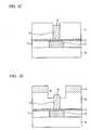
- FIGS. 1A to FIG. 1GA known method of forming an interconnection line for a semiconductor device is described with reference to FIGS. 1A to FIG. 1G .
- a semiconductor substrate 10 on which a lower insulating layer 11 and a first interconnection line 12 are formedis provided.
- An etch stop layer 13is then formed on the entire surface of the substrate, and an intermediate insulating layer 14 of an oxide layer is formed on the etch stop layer 13 .
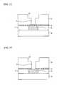
- a first photoresist pattern(not shown) is formed on the intermediate insulating layer 14 by a photolithography process, and the intermediate insulating layer 14 is then etched by an etching process using the first photoresist pattern as an etching mask, to form a via hole 15 exposing the portion of the etch stop layer 13 over the first interconnection line 12 . Thereafter, the first photoresist pattern is removed by a well-known method.
- a sacrificial layer 16is formed on the intermediate insulating layer 14 to fill the via hole 15 .
- the sacrificial layer 16is then removed to expose the intermediate insulating layer and to form a recess over the sacrificial layer 16 of the via hole 15 .
- the sacrificial layer 16is formed of a photoresist layer.
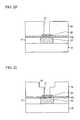
- a second photoresist pattern 17is formed on the intermediate insulating layer 14 by a photolithography process, and the portion of the intermediate insulating layer 14 is then etched by an etching process using the second photoresist pattern 17 as an etch mask, to form a trench 18 including the via hole 15 at the upper portion of the via hole 15 .
- the second photoresist pattern 17is removed by a well-known method.
- the sacrificial layer 16is also removed, to expose the etch stop layer 13 at the bottom of the via hole 15 .
- the exposed portion of the etch stop layer 13is removed, to expose the first interconnection layer 12 at the bottom of the via hole 15 .
- a Cu layeris formed on the intermediate insulating layer 14 to fill the via hole 15 and the trench 18 , and a planarization process is then performed to expose the intermediate insulating layer 14 , thereby forming a second interconnection line 19 that is electrically connected to the first interconnection line 12 .
- the etch stop layer 13stops the intermediate insulating layer 14 from being etched to prevent damage to the first interconnection line 12 due to the etching. Therefore, a material having high etch selectivity to the intermediate insulating layer 14 such as, for example, a nitride layer must be used as the etch stop layer 13 .
- the nitride layerhas problems in that RC delay increases and the speed of a device manufactured thereby is deteriorated because it has a relatively high dielectric constant (high-k) compared with the oxide layer.
- an insulating layer of a low dielectric constant (low-k)has been used as the intermediate insulating layer 14 , but it is difficult to obtain good effects if the etch stop layer 13 at the bottom of the via hole 15 is not fully removed.
- the etch stop layer 13remains at the bottom of the via hole 15 because a polymer (not shown) remains over the sacrificial layer 16 when etching the intermediate insulating layer 14 for forming the trench 18 , and this prevents the sacrificial layer 16 from being removed when removing the second photoresist pattern 17 for the sacrificial layer 16 to remain in the via hole 15 , so that the etch stop layer 13 is not fully removed when removing the etch stop layer 13 .
- the sacrificial layer 16 remaining in the via hole 15must be fully removed by additionally performing a washing or a post etch treatment (PET), but there is problem in that this causes process time and fabrication cost to increase
- FIGS. 1A to 1 Gare cross-sectional views depicting a known method of forming an interconnection line for a semiconductor device.
- FIGS. 2A to 2 Fare cross-sectional views depicting an example method of forming an interconnection line for a semiconductor device.
- the example methods and apparatus described hereinprovide an interconnection line of a semiconductor device that is capable of preventing a lower interconnection line from being damaged when etching an intermediate insulating layer for forming a via hole and a trench, and reducing RC delay.
- the example interconnection line disclosed hereinincludes: a semiconductor substrate; a first interconnection line formed on the substrate; an insulating layer pattern formed on the substrate to expose the portion of the first interconnection line; a metal pad layer formed on the exposed portion of the first interconnection line; an intermediate insulating layer formed on the entire surface of the substrate and having a via hole and a trench exposing the metal pad layer; and a second interconnection formed in the via hole and the trench and electrically connected to the first interconnection line through the metal pad layer.
- An example method of forming the interconnection line for a semiconductor device described hereinincludes: providing a semiconductor substrate on which a first interconnection line is formed; forming an insulating layer pattern exposing a portion of the first interconnection line on the substrate; forming a metal pad layer on the exposed portion of the first interconnection line; forming an intermediate insulating layer on the entire surface of the substrate; etching the intermediate insulating layer to form a via hole exposing the metal pad layer; etching a portion of the intermediate insulating layer to form a trench at the upper portion of the via hole; and forming a second interconnection line electrically connected to the first interconnection line through the metal pad layer in the via hole and the trench.
- the insulating layer pattern and the intermediate insulating layerare respectively formed of one selected from a silicon oxide (SiO2) layer, an FSG (Fluoro-Silicate Glass) layer, and an insulating layer of a low dielectric constant (low-k) of below 3.0.
- the metal pad layeris formed of one selected from a W layer, a Ti layer, a TiN layer, a Ta layer and a TaN layer.
- FIGS. 2A to FIG. 2FAn example method of forming an interconnection line for a semiconductor device is described with reference to FIGS. 2A to FIG. 2F .
- a semiconductor substrate 20 on which a lower insulating layer 21 and a first interconnection line 22 are formedis provided.
- the first interconnection line 22is formed of a Cu layer.
- an insulating layer 23is relatively thinly formed on the entire surface of the substrate, and a first photoresist pattern 24 exposing the portion of the insulating layer 23 over the first interconnection line 22 is formed on the insulating layer 23 by a photolithography process.
- the insulating layer 23is formed of one selected from a silicon oxide (SiO2) layer, an FSG (Fluoro-Silicate Glass) layer, and an insulating layer of a low dielectric constant (low-k) of below 3.0. Furthermore, the first photoresist pattern 24 is thinly formed to provide as accurate an alignment as possible.
- the insulating layer 23is etched by an etching process using a first photoresist pattern 24 (referring to FIG. 2A ) as an etch mask to form an insulating pattern 23 a exposing the portion of the first interconnection line 22 .
- a first photoresist pattern 24(referring to FIG. 2A ) as an etch mask to form an insulating pattern 23 a exposing the portion of the first interconnection line 22 .
- the surface area of the first interconnection line 21 exposed by the insulating pattern 23 ais as large as possible.
- the first photoresist pattern 24is removed by a well-known method.
- a metal pad layer 25is selectively formed on the exposed portion of the first interconnection line 22 by a selective deposition method.
- the metal pad layer 24is formed of one selected from a W layer, a Ti layer, a TiN layer, a Ta layer and a TaN layer.
- the metal pad layer 25is formed to have as large a surface area, within a range in which a short-circuit with adjacent conductive layers (not shown) does not occur, as possible.
- an intermediate insulating layer 26is formed on the entire surface of the substrate to cover the insulating layer pattern 23 a and the metal pad layer 25 .
- the intermediate insulating layer 26is formed of one selected from a silicon oxide (SiO2) layer, an FSG (Fluoro-Silicate Glass) layer and an insulating layer of a low dielectric constant (low-k) of below 3.0 the same as the insulating layer 23 .
- a second photoresist pattern(not shown) is formed on the intermediate insulating layer 23 by a photolithography process, and the intermediate insulating layer 26 is etched by an etching process using the second photoresist pattern as an etch mask to form a via hole 27 exposing the metal pad layer 25 .
- the first interconnection line 22is protected by the metal pad layer 25 so that damage due to the etching does not occur at the first interconnection line 22 .
- the second photoresist patternis then removed by a well-known method.
- a third photoresist pattern(not shown) is formed on the intermediate insulating layer 26 by a photolithography process, and the portion of the intermediate insulating layer 26 is etched by an etching process using the third photoresist pattern as an etch mask, to form a trench 28 including the via hole 27 at the upper portion of the via hole 27 .
- the first interconnection line 22is also protected by the metal pad layer 25 so that damage due to the etching does not occur at the first interconnection line 22 .
- the third photoresist patternis then removed by a well-known method.
- a Cu layeris formed on the intermediate insulating layer 26 by an electroless plating method or an electroplating method so as to fill the via hole 27 and the trench 28 .
- a planarization processis performed by a chemical mechanical polishing (CMP) to expose intermediate insulating layer 26 , thereby forming a second interconnection line 29 that is electrically connected to the first interconnection layer 22 through the metal pad layer 25 .
- CMPchemical mechanical polishing
- the metal pad layeris selectively formed on the first interconnection line and then the etching process for forming the via hole and the trench are respectively performed.
- the above-described methodcan reduce RC delay owing to forming the intermediate insulating layer and the insulating layer pattern with the insulating layer of a low dielectric constant (low-k) and can improve the yield and the reliability of a manufactured device.
Landscapes
- Engineering & Computer Science (AREA)
- Physics & Mathematics (AREA)
- Condensed Matter Physics & Semiconductors (AREA)
- General Physics & Mathematics (AREA)
- Manufacturing & Machinery (AREA)
- Computer Hardware Design (AREA)
- Microelectronics & Electronic Packaging (AREA)
- Power Engineering (AREA)
- Internal Circuitry In Semiconductor Integrated Circuit Devices (AREA)
Abstract
Description
- This application is a divisional of U.S. patent application Ser. No. 11/026,717, filed Dec. 30, 2004, pending.
- The present disclosure relates to a semiconductor device, and more particularly, to an interconnection line of a semiconductor device and a method of forming the same using a dual damascene process.
- Aluminum (Al) has mainly been used as an interconnection line material for a semiconductor device in the past. However, copper (Cu) has been recently used as an interconnection line material instead of Al, because the integration density and the speed of semiconductor devices have increased, so the line width of the interconnection lines has been reduced, thereby decreasing their resistance and contact resistance and reducing occurrence of electro migration (EM), is disclosed in U.S. Pat. No. 6,198,170.
- As Cu has low resistivity and high resistance against EM compared with Al, it can provide high reliability when used an interconnection line for a high integration density device and a high-speed device. On the other hand, as it is impossible to pattern Cu by dry etching, to form a Cu interconnection line, a dual damascene process is used to form a via hole and a trench in an intermediate insulating layer, the via hole and the trench are filled with Cu, and a planarization process must be performed.
- A known method of forming an interconnection line for a semiconductor device is described with reference to
FIGS. 1A toFIG. 1G . As shown inFIG. 1A , asemiconductor substrate 10 on which a lowerinsulating layer 11 and afirst interconnection line 12 are formed, is provided. Anetch stop layer 13 is then formed on the entire surface of the substrate, and an intermediate insulatinglayer 14 of an oxide layer is formed on theetch stop layer 13. - As shown in
FIG. 1B , a first photoresist pattern (not shown) is formed on the intermediate insulatinglayer 14 by a photolithography process, and theintermediate insulating layer 14 is then etched by an etching process using the first photoresist pattern as an etching mask, to form avia hole 15 exposing the portion of theetch stop layer 13 over thefirst interconnection line 12. Thereafter, the first photoresist pattern is removed by a well-known method. - As shown in
FIG. 1C , asacrificial layer 16 is formed on the intermediate insulatinglayer 14 to fill thevia hole 15. Thesacrificial layer 16 is then removed to expose the intermediate insulating layer and to form a recess over thesacrificial layer 16 of thevia hole 15. Thesacrificial layer 16 is formed of a photoresist layer. - As shown in
FIG. 1D , a secondphotoresist pattern 17 is formed on the intermediate insulatinglayer 14 by a photolithography process, and the portion of theintermediate insulating layer 14 is then etched by an etching process using the secondphotoresist pattern 17 as an etch mask, to form atrench 18 including thevia hole 15 at the upper portion of thevia hole 15. - As shown in
FIG. 1E , thesecond photoresist pattern 17 is removed by a well-known method. At this time, thesacrificial layer 16 is also removed, to expose theetch stop layer 13 at the bottom of thevia hole 15. - As shown in
FIG. 1F , the exposed portion of theetch stop layer 13 is removed, to expose thefirst interconnection layer 12 at the bottom of thevia hole 15. - As shown in
FIG. 1G , a Cu layer is formed on the intermediate insulatinglayer 14 to fill thevia hole 15 and thetrench 18, and a planarization process is then performed to expose theintermediate insulating layer 14, thereby forming asecond interconnection line 19 that is electrically connected to thefirst interconnection line 12. - In the known method of forming the interconnection line as described above, when forming the
via hole 15, theetch stop layer 13 stops the intermediate insulatinglayer 14 from being etched to prevent damage to thefirst interconnection line 12 due to the etching. Therefore, a material having high etch selectivity to the intermediate insulatinglayer 14 such as, for example, a nitride layer must be used as theetch stop layer 13. - However, the nitride layer has problems in that RC delay increases and the speed of a device manufactured thereby is deteriorated because it has a relatively high dielectric constant (high-k) compared with the oxide layer. To overcome these problems, an insulating layer of a low dielectric constant (low-k) has been used as the intermediate
insulating layer 14, but it is difficult to obtain good effects if theetch stop layer 13 at the bottom of thevia hole 15 is not fully removed. - Here, the
etch stop layer 13 remains at the bottom of thevia hole 15 because a polymer (not shown) remains over thesacrificial layer 16 when etching the intermediate insulatinglayer 14 for forming thetrench 18, and this prevents thesacrificial layer 16 from being removed when removing thesecond photoresist pattern 17 for thesacrificial layer 16 to remain in thevia hole 15, so that theetch stop layer 13 is not fully removed when removing theetch stop layer 13. - Accordingly, to prevent the
etch stop layer 13 from remaining at the bottom of thevia hole 15, thesacrificial layer 16 remaining in thevia hole 15 must be fully removed by additionally performing a washing or a post etch treatment (PET), but there is problem in that this causes process time and fabrication cost to increase FIGS. 1A to1G are cross-sectional views depicting a known method of forming an interconnection line for a semiconductor device.FIGS. 2A to2F are cross-sectional views depicting an example method of forming an interconnection line for a semiconductor device.- In general, the example methods and apparatus described herein provide an interconnection line of a semiconductor device that is capable of preventing a lower interconnection line from being damaged when etching an intermediate insulating layer for forming a via hole and a trench, and reducing RC delay.
- In general, the example interconnection line disclosed herein includes: a semiconductor substrate; a first interconnection line formed on the substrate; an insulating layer pattern formed on the substrate to expose the portion of the first interconnection line; a metal pad layer formed on the exposed portion of the first interconnection line; an intermediate insulating layer formed on the entire surface of the substrate and having a via hole and a trench exposing the metal pad layer; and a second interconnection formed in the via hole and the trench and electrically connected to the first interconnection line through the metal pad layer.
- An example method of forming the interconnection line for a semiconductor device described herein includes: providing a semiconductor substrate on which a first interconnection line is formed; forming an insulating layer pattern exposing a portion of the first interconnection line on the substrate; forming a metal pad layer on the exposed portion of the first interconnection line; forming an intermediate insulating layer on the entire surface of the substrate; etching the intermediate insulating layer to form a via hole exposing the metal pad layer; etching a portion of the intermediate insulating layer to form a trench at the upper portion of the via hole; and forming a second interconnection line electrically connected to the first interconnection line through the metal pad layer in the via hole and the trench.
- Furthermore, the insulating layer pattern and the intermediate insulating layer are respectively formed of one selected from a silicon oxide (SiO2) layer, an FSG (Fluoro-Silicate Glass) layer, and an insulating layer of a low dielectric constant (low-k) of below 3.0. Additionally, the metal pad layer is formed of one selected from a W layer, a Ti layer, a TiN layer, a Ta layer and a TaN layer.
- An example method of forming an interconnection line for a semiconductor device is described with reference to
FIGS. 2A toFIG. 2F . As shown inFIG. 2A , asemiconductor substrate 20 on which a lowerinsulating layer 21 and afirst interconnection line 22 are formed is provided. Thefirst interconnection line 22 is formed of a Cu layer. Then, aninsulating layer 23 is relatively thinly formed on the entire surface of the substrate, and a firstphotoresist pattern 24 exposing the portion of theinsulating layer 23 over thefirst interconnection line 22 is formed on theinsulating layer 23 by a photolithography process. Theinsulating layer 23 is formed of one selected from a silicon oxide (SiO2) layer, an FSG (Fluoro-Silicate Glass) layer, and an insulating layer of a low dielectric constant (low-k) of below 3.0. Furthermore, the firstphotoresist pattern 24 is thinly formed to provide as accurate an alignment as possible. - As shown in
FIG. 2B , theinsulating layer 23 is etched by an etching process using a first photoresist pattern24 (referring toFIG. 2A ) as an etch mask to form aninsulating pattern 23aexposing the portion of thefirst interconnection line 22. Here, it is preferable that the surface area of thefirst interconnection line 21 exposed by theinsulating pattern 23ais as large as possible. Thereafter, thefirst photoresist pattern 24 is removed by a well-known method. - As shown in
FIG. 2C , ametal pad layer 25 is selectively formed on the exposed portion of thefirst interconnection line 22 by a selective deposition method. Themetal pad layer 24 is formed of one selected from a W layer, a Ti layer, a TiN layer, a Ta layer and a TaN layer. Furthermore, themetal pad layer 25 is formed to have as large a surface area, within a range in which a short-circuit with adjacent conductive layers (not shown) does not occur, as possible. - As shown in
FIG. 2D , an intermediate insulatinglayer 26 is formed on the entire surface of the substrate to cover the insulatinglayer pattern 23aand themetal pad layer 25. The intermediate insulatinglayer 26 is formed of one selected from a silicon oxide (SiO2) layer, an FSG (Fluoro-Silicate Glass) layer and an insulating layer of a low dielectric constant (low-k) of below 3.0 the same as the insulatinglayer 23. Thereafter, a second photoresist pattern (not shown) is formed on the intermediate insulatinglayer 23 by a photolithography process, and the intermediate insulatinglayer 26 is etched by an etching process using the second photoresist pattern as an etch mask to form a viahole 27 exposing themetal pad layer 25. At this time, thefirst interconnection line 22 is protected by themetal pad layer 25 so that damage due to the etching does not occur at thefirst interconnection line 22. The second photoresist pattern is then removed by a well-known method. - As shown in
FIG. 2E , a third photoresist pattern (not shown) is formed on the intermediate insulatinglayer 26 by a photolithography process, and the portion of the intermediate insulatinglayer 26 is etched by an etching process using the third photoresist pattern as an etch mask, to form atrench 28 including the viahole 27 at the upper portion of the viahole 27. At this time, thefirst interconnection line 22 is also protected by themetal pad layer 25 so that damage due to the etching does not occur at thefirst interconnection line 22. The third photoresist pattern is then removed by a well-known method. - As shown in
FIG. 2F , a Cu layer is formed on the intermediate insulatinglayer 26 by an electroless plating method or an electroplating method so as to fill the viahole 27 and thetrench 28. A planarization process is performed by a chemical mechanical polishing (CMP) to expose intermediate insulatinglayer 26, thereby forming asecond interconnection line 29 that is electrically connected to thefirst interconnection layer 22 through themetal pad layer 25. - In the example described above, the metal pad layer is selectively formed on the first interconnection line and then the etching process for forming the via hole and the trench are respectively performed.
- As a result of the above-described method, damage to the first interconnection line by etching can be prevented. Additionally, problems due to some of the etch stop layer remaining can be overcome, as there is no need to use nitride layer etch stop layer. Still further, the above-described method can reduce RC delay owing to forming the intermediate insulating layer and the insulating layer pattern with the insulating layer of a low dielectric constant (low-k) and can improve the yield and the reliability of a manufactured device.
- While the examples herein have been described in detail with reference to example embodiments, it is to be understood that the coverage of this patent is not limited to the disclosed embodiments, but, on the contrary, is intended to cover various modifications and equivalent arrangements included within the sprit and scope of the appended claims.
Claims (5)
Priority Applications (1)
| Application Number | Priority Date | Filing Date | Title |
|---|---|---|---|
| US11/788,794US7960839B2 (en) | 2003-12-31 | 2007-04-20 | Semiconductor interconnection line and method of forming the same |
Applications Claiming Priority (4)
| Application Number | Priority Date | Filing Date | Title |
|---|---|---|---|
| KR10-2003-0101806 | 2003-12-31 | ||
| KR1020030101806AKR100552815B1 (en) | 2003-12-31 | 2003-12-31 | Dual damascene wiring formation method of semiconductor device |
| US11/026,717US7223686B2 (en) | 2003-12-31 | 2004-12-30 | Semiconductor interconnection line and method of forming the same |
| US11/788,794US7960839B2 (en) | 2003-12-31 | 2007-04-20 | Semiconductor interconnection line and method of forming the same |
Related Parent Applications (1)
| Application Number | Title | Priority Date | Filing Date |
|---|---|---|---|
| US11/026,717DivisionUS7223686B2 (en) | 2003-12-31 | 2004-12-30 | Semiconductor interconnection line and method of forming the same |
Publications (2)
| Publication Number | Publication Date |
|---|---|
| US20070194448A1true US20070194448A1 (en) | 2007-08-23 |
| US7960839B2 US7960839B2 (en) | 2011-06-14 |
Family
ID=34698913
Family Applications (2)
| Application Number | Title | Priority Date | Filing Date |
|---|---|---|---|
| US11/026,717Expired - LifetimeUS7223686B2 (en) | 2003-12-31 | 2004-12-30 | Semiconductor interconnection line and method of forming the same |
| US11/788,794Active2028-02-04US7960839B2 (en) | 2003-12-31 | 2007-04-20 | Semiconductor interconnection line and method of forming the same |
Family Applications Before (1)
| Application Number | Title | Priority Date | Filing Date |
|---|---|---|---|
| US11/026,717Expired - LifetimeUS7223686B2 (en) | 2003-12-31 | 2004-12-30 | Semiconductor interconnection line and method of forming the same |
Country Status (2)
| Country | Link |
|---|---|
| US (2) | US7223686B2 (en) |
| KR (1) | KR100552815B1 (en) |
Families Citing this family (6)
| Publication number | Priority date | Publication date | Assignee | Title |
|---|---|---|---|---|
| KR100552815B1 (en)* | 2003-12-31 | 2006-02-22 | 동부아남반도체 주식회사 | Dual damascene wiring formation method of semiconductor device |
| US7779268B2 (en)* | 2004-12-07 | 2010-08-17 | Mitsubishi Electric Research Laboratories, Inc. | Biometric based user authentication and data encryption |
| KR100643853B1 (en)* | 2005-06-04 | 2006-11-14 | 삼성전자주식회사 | Method for forming damascene wiring of semiconductor device and semiconductor device manufactured thereby |
| KR100669851B1 (en)* | 2005-07-12 | 2007-01-16 | 삼성전자주식회사 | Manufacturing Method of Phase Change Memory Device |
| WO2010059747A2 (en)* | 2008-11-18 | 2010-05-27 | Workshare Technology, Inc. | Methods and systems for exact data match filtering |
| US11948874B2 (en)* | 2020-06-26 | 2024-04-02 | Intel Corporation | Vertically spaced intra-level interconnect line metallization for integrated circuit devices |
Citations (7)
| Publication number | Priority date | Publication date | Assignee | Title |
|---|---|---|---|---|
| US5939788A (en)* | 1998-03-11 | 1999-08-17 | Micron Technology, Inc. | Copper diffusion barrier, aluminum wetting layer and improved methods for filling openings in silicon substrates with cooper |
| US6084304A (en)* | 1998-05-01 | 2000-07-04 | United Microelectronics Corp. | Structure of metallization |
| US6559548B1 (en)* | 1999-03-19 | 2003-05-06 | Kabushiki Kaisha Toshiba | Wiring structure of semiconductor device |
| US6747355B2 (en)* | 2001-07-17 | 2004-06-08 | Nec Electronics Corporation | Semiconductor device and method for manufacturing the same |
| US6879042B2 (en)* | 2000-06-20 | 2005-04-12 | Nec Electronics Corporation | Semiconductor device and method and apparatus for manufacturing the same |
| US7056820B2 (en)* | 2003-11-20 | 2006-06-06 | International Business Machines Corporation | Bond pad |
| US7223686B2 (en)* | 2003-12-31 | 2007-05-29 | Dongbu Electronics Co., Ltd. | Semiconductor interconnection line and method of forming the same |
- 2003
- 2003-12-31KRKR1020030101806Apatent/KR100552815B1/ennot_activeExpired - Fee Related
- 2004
- 2004-12-30USUS11/026,717patent/US7223686B2/ennot_activeExpired - Lifetime
- 2007
- 2007-04-20USUS11/788,794patent/US7960839B2/enactiveActive
Patent Citations (7)
| Publication number | Priority date | Publication date | Assignee | Title |
|---|---|---|---|---|
| US5939788A (en)* | 1998-03-11 | 1999-08-17 | Micron Technology, Inc. | Copper diffusion barrier, aluminum wetting layer and improved methods for filling openings in silicon substrates with cooper |
| US6084304A (en)* | 1998-05-01 | 2000-07-04 | United Microelectronics Corp. | Structure of metallization |
| US6559548B1 (en)* | 1999-03-19 | 2003-05-06 | Kabushiki Kaisha Toshiba | Wiring structure of semiconductor device |
| US6879042B2 (en)* | 2000-06-20 | 2005-04-12 | Nec Electronics Corporation | Semiconductor device and method and apparatus for manufacturing the same |
| US6747355B2 (en)* | 2001-07-17 | 2004-06-08 | Nec Electronics Corporation | Semiconductor device and method for manufacturing the same |
| US7056820B2 (en)* | 2003-11-20 | 2006-06-06 | International Business Machines Corporation | Bond pad |
| US7223686B2 (en)* | 2003-12-31 | 2007-05-29 | Dongbu Electronics Co., Ltd. | Semiconductor interconnection line and method of forming the same |
Also Published As
| Publication number | Publication date |
|---|---|
| KR20050071027A (en) | 2005-07-07 |
| KR100552815B1 (en) | 2006-02-22 |
| US20050140020A1 (en) | 2005-06-30 |
| US7960839B2 (en) | 2011-06-14 |
| US7223686B2 (en) | 2007-05-29 |
Similar Documents
| Publication | Publication Date | Title |
|---|---|---|
| US6071809A (en) | Methods for forming high-performing dual-damascene interconnect structures | |
| US8299617B2 (en) | Method and apparatus for forming metal-metal oxide etch stop/barrier for integrated circuit interconnects | |
| US6268283B1 (en) | Method for forming dual damascene structure | |
| US20060205204A1 (en) | Method of making a semiconductor interconnect with a metal cap | |
| US6372635B1 (en) | Method for making a slot via filled dual damascene low k interconnect structure without middle stop layer | |
| KR100860133B1 (en) | Local Increase in Sidewall Density by Ion Implantation | |
| KR20200029835A (en) | Method of Fabricating Interconnection Line of Semiconductor Device and Interconnection Line of Semiconductor Device by The Same | |
| US7960839B2 (en) | Semiconductor interconnection line and method of forming the same | |
| US7138714B2 (en) | Via barrier layers continuous with metal line barrier layers at notched or dielectric mesa portions in metal lines | |
| US7022600B2 (en) | Method of forming dual damascene interconnection using low-k dielectric material | |
| US6638849B2 (en) | Method for manufacturing semiconductor devices having copper interconnect and low-K dielectric layer | |
| US6674170B1 (en) | Barrier metal oxide interconnect cap in integrated circuits | |
| US6320263B1 (en) | Semiconductor metalization barrier and manufacturing method therefor | |
| US6583051B2 (en) | Method of manufacturing an amorphized barrier layer for integrated circuit interconnects | |
| US20020127849A1 (en) | Method of manufacturing dual damascene structure | |
| US6465343B1 (en) | Method for forming backend interconnect with copper etching and ultra low-k dielectric materials | |
| US7648870B2 (en) | Method of forming fuse region in semiconductor damascene process | |
| US6590288B1 (en) | Selective deposition in integrated circuit interconnects | |
| US6455938B1 (en) | Integrated circuit interconnect shunt layer | |
| KR100539221B1 (en) | Method of manufacturing electrical interconnection for semiconductor device | |
| US6462416B1 (en) | Gradated barrier layer in integrated circuit interconnects | |
| US6476498B1 (en) | Elimination of flux divergence in integrated circuit interconnects | |
| JP2004503089A (en) | Via-first dual damascene method for copper metallization | |
| JP2004503089A6 (en) | Via-first dual damascene method for copper metallization | |
| KR100784105B1 (en) | Manufacturing Method of Semiconductor Device |
Legal Events
| Date | Code | Title | Description |
|---|---|---|---|
| FEPP | Fee payment procedure | Free format text:PAYOR NUMBER ASSIGNED (ORIGINAL EVENT CODE: ASPN); ENTITY STATUS OF PATENT OWNER: LARGE ENTITY | |
| STCF | Information on status: patent grant | Free format text:PATENTED CASE | |
| FEPP | Fee payment procedure | Free format text:PAT HOLDER CLAIMS SMALL ENTITY STATUS, ENTITY STATUS SET TO SMALL (ORIGINAL EVENT CODE: LTOS); ENTITY STATUS OF PATENT OWNER: LARGE ENTITY | |
| FEPP | Fee payment procedure | Free format text:PAYER NUMBER DE-ASSIGNED (ORIGINAL EVENT CODE: RMPN); ENTITY STATUS OF PATENT OWNER: LARGE ENTITY Free format text:PAYOR NUMBER ASSIGNED (ORIGINAL EVENT CODE: ASPN); ENTITY STATUS OF PATENT OWNER: LARGE ENTITY | |
| AS | Assignment | Owner name:INPHI CORPORATION, UNITED STATES Free format text:ASSIGNMENT OF ASSIGNORS INTEREST;ASSIGNOR:DONGBU HITEK, CO., LTD.;REEL/FRAME:034009/0157 Effective date:20141008 | |
| AS | Assignment | Owner name:INPHI CORPORATION, CALIFORNIA Free format text:CORRECTIVE ASSIGNMENT TO CORRECT REMOVE PATENT NO. 878209 FROM EXHIBIT B PREVIOUSLY RECORDED AT REEL: 034009 FRAME: 0157. ASSIGNOR(S) HEREBY CONFIRMS THE ASSIGNMENT;ASSIGNOR:DONGBU HITEK, CO., LTD.;REEL/FRAME:034087/0097 Effective date:20141008 | |
| FPAY | Fee payment | Year of fee payment:4 | |
| FEPP | Fee payment procedure | Free format text:PAYER NUMBER DE-ASSIGNED (ORIGINAL EVENT CODE: RMPN); ENTITY STATUS OF PATENT OWNER: LARGE ENTITY Free format text:PAYOR NUMBER ASSIGNED (ORIGINAL EVENT CODE: ASPN); ENTITY STATUS OF PATENT OWNER: LARGE ENTITY | |
| AS | Assignment | Owner name:INPHI CORPORATION, CALIFORNIA Free format text:ASSIGNMENT OF ASSIGNORS INTEREST;ASSIGNOR:DONGBU HITEK, CO., LTD.;REEL/FRAME:041375/0822 Effective date:20141008 | |
| FEPP | Fee payment procedure | Free format text:ENTITY STATUS SET TO UNDISCOUNTED (ORIGINAL EVENT CODE: BIG.) | |
| MAFP | Maintenance fee payment | Free format text:PAYMENT OF MAINTENANCE FEE, 8TH YEAR, LARGE ENTITY (ORIGINAL EVENT CODE: M1552); ENTITY STATUS OF PATENT OWNER: LARGE ENTITY Year of fee payment:8 | |
| AS | Assignment | Owner name:MARVELL TECHNOLOGY CAYMAN I, CAYMAN ISLANDS Free format text:ASSIGNMENT OF ASSIGNORS INTEREST;ASSIGNOR:INPHI CORPORATION;REEL/FRAME:056649/0823 Effective date:20210617 | |
| AS | Assignment | Owner name:CAVIUM INTERNATIONAL, CAYMAN ISLANDS Free format text:ASSIGNMENT OF ASSIGNORS INTEREST;ASSIGNOR:MARVELL TECHNOLOGY CAYMAN I;REEL/FRAME:057279/0519 Effective date:20210620 | |
| AS | Assignment | Owner name:MARVELL ASIA PTE LTD., SINGAPORE Free format text:ASSIGNMENT OF ASSIGNORS INTEREST;ASSIGNOR:CAVIUM INTERNATIONAL;REEL/FRAME:057336/0873 Effective date:20210620 | |
| MAFP | Maintenance fee payment | Free format text:PAYMENT OF MAINTENANCE FEE, 12TH YEAR, LARGE ENTITY (ORIGINAL EVENT CODE: M1553); ENTITY STATUS OF PATENT OWNER: LARGE ENTITY Year of fee payment:12 |