US20070193515A1 - Apparatus for generating remote plasma - Google Patents
Apparatus for generating remote plasmaDownload PDFInfo
- Publication number
- US20070193515A1 US20070193515A1US11/703,621US70362107AUS2007193515A1US 20070193515 A1US20070193515 A1US 20070193515A1US 70362107 AUS70362107 AUS 70362107AUS 2007193515 A1US2007193515 A1US 2007193515A1
- Authority
- US
- United States
- Prior art keywords
- plasma
- generating unit
- source
- guide holes
- purge gas
- Prior art date
- Legal status (The legal status is an assumption and is not a legal conclusion. Google has not performed a legal analysis and makes no representation as to the accuracy of the status listed.)
- Abandoned
Links
- 0*C1=CCCC1Chemical compound*C1=CCCC10.000description1
Images


Classifications
- H—ELECTRICITY
- H05—ELECTRIC TECHNIQUES NOT OTHERWISE PROVIDED FOR
- H05H—PLASMA TECHNIQUE; PRODUCTION OF ACCELERATED ELECTRICALLY-CHARGED PARTICLES OR OF NEUTRONS; PRODUCTION OR ACCELERATION OF NEUTRAL MOLECULAR OR ATOMIC BEAMS
- H05H1/00—Generating plasma; Handling plasma
- H05H1/24—Generating plasma
- H05H1/46—Generating plasma using applied electromagnetic fields, e.g. high frequency or microwave energy
- H—ELECTRICITY
- H01—ELECTRIC ELEMENTS
- H01J—ELECTRIC DISCHARGE TUBES OR DISCHARGE LAMPS
- H01J37/00—Discharge tubes with provision for introducing objects or material to be exposed to the discharge, e.g. for the purpose of examination or processing thereof
- H01J37/32—Gas-filled discharge tubes
- H01J37/32009—Arrangements for generation of plasma specially adapted for examination or treatment of objects, e.g. plasma sources
- H01J37/32082—Radio frequency generated discharge
- H01J37/321—Radio frequency generated discharge the radio frequency energy being inductively coupled to the plasma
- H01J37/3211—Antennas, e.g. particular shapes of coils
- H—ELECTRICITY
- H01—ELECTRIC ELEMENTS
- H01J—ELECTRIC DISCHARGE TUBES OR DISCHARGE LAMPS
- H01J37/00—Discharge tubes with provision for introducing objects or material to be exposed to the discharge, e.g. for the purpose of examination or processing thereof
- H01J37/32—Gas-filled discharge tubes
- H01J37/32009—Arrangements for generation of plasma specially adapted for examination or treatment of objects, e.g. plasma sources
- H01J37/32357—Generation remote from the workpiece, e.g. down-stream
- H—ELECTRICITY
- H01—ELECTRIC ELEMENTS
- H01J—ELECTRIC DISCHARGE TUBES OR DISCHARGE LAMPS
- H01J37/00—Discharge tubes with provision for introducing objects or material to be exposed to the discharge, e.g. for the purpose of examination or processing thereof
- H01J37/32—Gas-filled discharge tubes
- H01J37/32431—Constructional details of the reactor
- H01J37/3244—Gas supply means
- H—ELECTRICITY
- H01—ELECTRIC ELEMENTS
- H01J—ELECTRIC DISCHARGE TUBES OR DISCHARGE LAMPS
- H01J37/00—Discharge tubes with provision for introducing objects or material to be exposed to the discharge, e.g. for the purpose of examination or processing thereof
- H01J37/32—Gas-filled discharge tubes
- H01J37/32431—Constructional details of the reactor
- H01J37/32532—Electrodes
- H01J37/3255—Material
Definitions
- the present inventionrelates to an apparatus for generating remote plasma, and more particularly, to an apparatus for generating remote plasma that improves uniformity and quality of a thin film.
- a substrate electrode on which a substrate is mounted and an opposite electrodeare disposed in a vacuum chamber, and a high frequency voltage is then applied between the substrate electrode and the opposite electrode using high frequency power for electrode.
- plasmais generated in the vacuum chamber.
- the generated plasmadoes not uniformly react with the substrate mounted in the chamber so that it is difficult to form a thin film uniformly.
- ionse.g., particularly, positive ions, generated at a plasma generating unit are supplied without any control, which leads to a problem that the substrate or the thin film is damaged.
- An object of the present inventionis to provide an apparatus for generating remote plasma that can supply plasma generation gas to a substrate uniformly to improve a uniformity of a thin film.
- Another object of the present inventionis to provide an apparatus for generating remote plasma that can appropriately control positive ions generated with plasma to improve a quality of a thin film.
- an apparatus for generating a remote plasmaincluding: an RF (radio frequency) antenna disposed in regard to a chamber; a plasma generating unit formed in an uppermost portion of the chamber, wherein a plurality of plasma generation gas introduction pipes are communicated with the plasma generating unit; a first shower head disposed below the plasma generating unit, and having a plurality of first plasma guide holes; a second shower head disposed below the first shower head, and having a plurality of source/purge gas guide holes and a plurality of second plasma guide holes directly connected to the respective first plasma guide holes; and a source/purge gas introduction unit disposed between the first and second shower heads, wherein a plurality of source/purge gas introduction pipes are uniformly communicated with the source/purge gas introduction unit.
- the apparatusmay further include a DC bias generating unit disposed between the plasma generating unit and the first shower head.
- the DC bias generating unitmay have the shape of a grid, and may be formed of metallic material of which a surface is anodized.
- An inlet and an outlet of each of the first plasma, second plasma and source/purge gas guide holes, and an outlet of each of the plasma generation gas and source/purge gas introduction pipesmay be tapered such that its diameter becomes greater as it gets closer to an end thereof.
- the first plasma guide holesmay be radially arranged in the first shower head, and the second plasma guide holes and the source/purge gas guide holes may be radially and alternately arranged in the second shower head.
- the plurality of plasma generation gas introduction pipesmay be communicated with the plasma generating unit through an upper portion thereof or a side portion thereof.
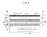
- FIG. 1is a sectional view of an apparatus for generating remote plasma according to one embodiment of the present invention
- FIGS. 2A and 2Bare plan views illustrating the apparatus for generating the remote plasma of FIG. 1 ;
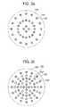
- FIG. 3Ais a sectional view taken along line 3 a - 3 a of FIG. 1
- FIG. 3Bis a sectional view taken along line 3 b - 3 b of FIG. 1 ;
- FIG. 4is a sectional view illustrating a modified shape of a plasma guide pipe
- FIG. 5is a schematic view of a DC bias generating unit
- FIG. 6is a schematic view illustrating one example of an RF antenna
- FIG. 7is a sectional view of an apparatus for generating remote plasma according to another embodiment of the present invention.
- FIG. 1is a sectional view of an apparatus for generating remote plasma according to one embodiment of the present invention
- An apparatus for generating remote plasmaincludes a radio frequency (RF) antenna, a plasma generating unit 120 , a first shower head 130 , a source/purge gas introduction unit 140 , and a second shower head 150 .
- RFradio frequency
- the RF antenna 107is disposed over an insulating member 108 such as quartz of a chamber, and plays a role in generating plasma.
- the RF antenna 107may be configured such that plasma can be uniformly generated.
- At least two loop-type antenna elements 10 and 20are horizontally spaced apart from each other by a predetermined distance such that they are overlapped with each other.
- the two loop-type antenna elements 10 and 20are electrically connected in parallel.
- a power supply terminal P and a ground terminal Gare formed at one end and the other end of each of the loop-type antenna elements 10 and 20 , respectively.
- the power supply terminal P and the ground terminal Gare disposed symmetrically with respect to a center of each of the antennal elements 10 and 20 .
- a horizontally bent portion 10 a of the antenna element 10is disposed between the power supply and ground terminals P and G of the other antenna element 20 .
- a horizontally bent portion 20 a of the antenna element 20is disposed between the power supply and ground terminals P and G of the other antenna element 10 .
- a total impedance of the antennais lowered because the antenna elements 10 and 20 are electrically connected in parallel, and thus it is possible to apply a low voltage.
- the horizontally bent portions 10 a and 20 aplay a role in complementing disconnected portions between the power supply terminal P and the ground terminal G. Accordingly, an antenna current is not cut off but is continued.
- there is no electric field differencebecause the bent portions 10 a and 20 a are horizontally bent at a central portion of each antenna element, which makes it possible to distribute plasma uniformly.
- a plasma generating unit 110is formed in an upper portion of the chamber, and is isolated from an exterior by means of the insulating member 108 such as quartz.
- a plurality of plasma generation gas introduction pipes 102are communicated with the plasma generating unit 110 uniformly. This means that portions where the plasma generation gas introduction pipes 102 are communicated with the plasma generating unit 110 are uniformly arranged.
- the plurality of plasma generation gas introduction pipes 102are communicated with the plasma generating unit 110 through an upper portion of the plasma generating unit 110 . According to another embodiment of FIG. 7 , however, the plurality of plasma generation gas introduction pipes 102 are communicated with the plasma generating unit 110 through a side portion of the plasma generating unit 110 .
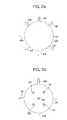
- the plurality of plasma generation gas introduction pipes 102are uniformly arranged on an entire surface as illustrated in FIG. 2A . In another embodiment, the plurality of plasma generation gas introduction pipes 102 are disposed on a side portion such that they are separated from each other at a predetermined rotation angle, as illustrated in FIG. 2B .
- the number of the plurality of plasma generation gas introduction pipes 102is 5 and 4 in FIGS. 2A and 2B , respectively, the number of the plurality of plasma generation gas introduction pipes 102 is not limited to it.
- the DC bias generating unit 120is disposed under the plasma generating unit 110 .
- the DC bias generating unit 120has the shape of a grid 122 such that plasma passes therethrough.
- the DC bias generating unit 120is formed of metallic material, and its surface is anodized.
- the first shower head 130is disposed in which a plurality of first plasma guide holes 132 are formed.
- the plurality of first plasma guide holes 132may be radially formed. As it will be described later, a plasma guide pipe 156 may be inserted into the first plasma guide hole 132 , wherein the plasma guide pipe 156 is connected from the first plasma guide hole to a second plasma guide hole 154 .
- a source/purge gas introduction unit 140is formed between the first shower head 130 and the second shower head 150 .
- a plurality of source/purge gas introduction pipes 104are disposed on side portions of the source/purge gas introduction unit 140 such that they are communicated with the source/purge gas introduction unit 140 .
- second plasma guide holes 154 and source/purge gas guide holes 152are radially and alternately disposed in the second shower head 150 , respectively.
- the plurality of source/purge gas introduction pipes 104are disposed such that they are spaced apart from each other at a predetermined rotation angle.
- a source/purge gas guide pipe 157may be inserted into the source/purge gas guide hole 152 .
- the plasma guide pipe 156extends from the first shower head 130 to the second shower head 150 through the source/purge gas introduction unit 140 .
- the plasma guide pipe 156has an inlet and an outlet of which each one may have tapered sidewalls 156 a and 157 a such that its diameter becomes greater as it gets closer to an end thereof.
- This constitutioncan also be identically applied to outlets of the plasma generation gas introduction pipe 102 and the source/purge gas introduction pipe 104 .
- uniform plasmais generated by means of plasma generation gas supplied through the plurality of plasma generation gas introduction pipes, and then is provided to the substrate through the plurality of plasma guide holes.
- source/purge gas supplied through the plurality of source/purge gas introduction pipeis provided to the substrate through a plurality of source/purge gas introduction hole, and thus it is possible to form the thin film uniformly.
- the damage of the substrate and the thin filmcan be prevented by reliably trapping the positive ions generated with plasma in virtue of the DC bias generating unit, it is possible to improve the quality of the thin film.
- plasma generation gasis supplied to a substrate uniformly, whereby the uniformity of the thin film can be enhanced.
- the quality of the thin filmcan be enhanced by appropriately controlling positive ions generated with plasma.
Landscapes
- Physics & Mathematics (AREA)
- Engineering & Computer Science (AREA)
- Plasma & Fusion (AREA)
- Chemical & Material Sciences (AREA)
- Analytical Chemistry (AREA)
- Electromagnetism (AREA)
- Spectroscopy & Molecular Physics (AREA)
- Plasma Technology (AREA)
- Chemical Vapour Deposition (AREA)
- Drying Of Semiconductors (AREA)
Abstract
Description
- 1. Field of the Invention
- The present invention relates to an apparatus for generating remote plasma, and more particularly, to an apparatus for generating remote plasma that improves uniformity and quality of a thin film.
- 2. Description of the Related Art
- In recent years, as semiconductor devices shrink in size, it is required to perform plasma treatment under higher vacuum state for realizing a pattern or the like with high aspect ratio in dry etching, and filling a filling material into a hole or the like with high aspect ratio in plasma chemical vapor deposition (CVD) and atomic layer deposition (ALD).
- In a typical parallel plate type plasma generator, a substrate electrode on which a substrate is mounted and an opposite electrode are disposed in a vacuum chamber, and a high frequency voltage is then applied between the substrate electrode and the opposite electrode using high frequency power for electrode. Thus, plasma is generated in the vacuum chamber.
- However, according to the above constitution, the generated plasma does not uniformly react with the substrate mounted in the chamber so that it is difficult to form a thin film uniformly.
- Moreover, ions, e.g., particularly, positive ions, generated at a plasma generating unit are supplied without any control, which leads to a problem that the substrate or the thin film is damaged.
- An object of the present invention is to provide an apparatus for generating remote plasma that can supply plasma generation gas to a substrate uniformly to improve a uniformity of a thin film.
- Another object of the present invention is to provide an apparatus for generating remote plasma that can appropriately control positive ions generated with plasma to improve a quality of a thin film.
- According to an aspect of the present invention, there is provided an apparatus for generating a remote plasma, including: an RF (radio frequency) antenna disposed in regard to a chamber; a plasma generating unit formed in an uppermost portion of the chamber, wherein a plurality of plasma generation gas introduction pipes are communicated with the plasma generating unit; a first shower head disposed below the plasma generating unit, and having a plurality of first plasma guide holes; a second shower head disposed below the first shower head, and having a plurality of source/purge gas guide holes and a plurality of second plasma guide holes directly connected to the respective first plasma guide holes; and a source/purge gas introduction unit disposed between the first and second shower heads, wherein a plurality of source/purge gas introduction pipes are uniformly communicated with the source/purge gas introduction unit.
- The apparatus may further include a DC bias generating unit disposed between the plasma generating unit and the first shower head. The DC bias generating unit may have the shape of a grid, and may be formed of metallic material of which a surface is anodized.
- An inlet and an outlet of each of the first plasma, second plasma and source/purge gas guide holes, and an outlet of each of the plasma generation gas and source/purge gas introduction pipes may be tapered such that its diameter becomes greater as it gets closer to an end thereof.
- The first plasma guide holes may be radially arranged in the first shower head, and the second plasma guide holes and the source/purge gas guide holes may be radially and alternately arranged in the second shower head.
- The plurality of plasma generation gas introduction pipes may be communicated with the plasma generating unit through an upper portion thereof or a side portion thereof.
- The above objects and other advantages of the present invention will become more apparent by describing in detail preferred embodiments thereof with reference to the attached drawings in which:
FIG. 1 is a sectional view of an apparatus for generating remote plasma according to one embodiment of the present invention;FIGS. 2A and 2B are plan views illustrating the apparatus for generating the remote plasma ofFIG. 1 ;FIG. 3A is a sectional view taken along line3a-3aofFIG. 1 , andFIG. 3B is a sectional view taken alongline 3b-3bofFIG. 1 ;FIG. 4 is a sectional view illustrating a modified shape of a plasma guide pipe;FIG. 5 is a schematic view of a DC bias generating unit;FIG. 6 is a schematic view illustrating one example of an RF antenna; andFIG. 7 is a sectional view of an apparatus for generating remote plasma according to another embodiment of the present invention.- Now, preferred embodiments of the present invention will be described in detail with reference to the accompanying drawings.
FIG. 1 is a sectional view of an apparatus for generating remote plasma according to one embodiment of the present invention;- An apparatus for generating remote plasma includes a radio frequency (RF) antenna, a
plasma generating unit 120, afirst shower head 130, a source/purgegas introduction unit 140, and asecond shower head 150. - The
RF antenna 107 is disposed over aninsulating member 108 such as quartz of a chamber, and plays a role in generating plasma. TheRF antenna 107 may be configured such that plasma can be uniformly generated. - Specifically, referring to
FIG. 6 , at least two loop-type antenna elements10 and20 are horizontally spaced apart from each other by a predetermined distance such that they are overlapped with each other. The two loop-type antenna elements10 and20 are electrically connected in parallel. Herein, a power supply terminal P and a ground terminal G are formed at one end and the other end of each of the loop-type antenna elements10 and20, respectively. The power supply terminal P and the ground terminal G are disposed symmetrically with respect to a center of each of the antennal elements10 and20. A horizontally bent portion10aof the antenna element10 is disposed between the power supply and ground terminals P and G of the other antenna element20. Likewise, a horizontally bent portion20aof the antenna element20 is disposed between the power supply and ground terminals P and G of the other antenna element10. - A total impedance of the antenna is lowered because the antenna elements10 and20 are electrically connected in parallel, and thus it is possible to apply a low voltage. The horizontally bent portions10aand20aplay a role in complementing disconnected portions between the power supply terminal P and the ground terminal G. Accordingly, an antenna current is not cut off but is continued. In addition, there is no electric field difference because the bent portions10aand20aare horizontally bent at a central portion of each antenna element, which makes it possible to distribute plasma uniformly.
- A
plasma generating unit 110 is formed in an upper portion of the chamber, and is isolated from an exterior by means of theinsulating member 108 such as quartz. - According to the present invention, a plurality of plasma generation
gas introduction pipes 102 are communicated with theplasma generating unit 110 uniformly. This means that portions where the plasma generationgas introduction pipes 102 are communicated with theplasma generating unit 110 are uniformly arranged. - In one embodiment, the plurality of plasma generation
gas introduction pipes 102 are communicated with theplasma generating unit 110 through an upper portion of theplasma generating unit 110. According to another embodiment ofFIG. 7 , however, the plurality of plasma generationgas introduction pipes 102 are communicated with theplasma generating unit 110 through a side portion of theplasma generating unit 110. - In one embodiment, the plurality of plasma generation
gas introduction pipes 102 are uniformly arranged on an entire surface as illustrated inFIG. 2A . In another embodiment, the plurality of plasma generationgas introduction pipes 102 are disposed on a side portion such that they are separated from each other at a predetermined rotation angle, as illustrated inFIG. 2B . - Although the number of the plurality of plasma generation
gas introduction pipes 102 is5 and4 inFIGS. 2A and 2B , respectively, the number of the plurality of plasma generationgas introduction pipes 102 is not limited to it. - The DC
bias generating unit 120 is disposed under theplasma generating unit 110. Referring toFIG. 5 , preferably, the DCbias generating unit 120 has the shape of agrid 122 such that plasma passes therethrough. In addition, the DCbias generating unit 120 is formed of metallic material, and its surface is anodized. - In virtue of such a constitution, it is possible to prevent the damage of the substrate or the thin film, which may be caused by the trapping of the ions, i.e., positive ions, generated with plasma. Furthermore, since the surface of the DC
bias generating unit 120 is anodized, it is possible to prevent contamination due to metallic impurities during the generation of plasma. - Below the DC
bias generating unit 120, thefirst shower head 130 is disposed in which a plurality of firstplasma guide holes 132 are formed. - Referring to
FIG. 3A , the plurality of first plasma guide holes132 may be radially formed. As it will be described later, aplasma guide pipe 156 may be inserted into the firstplasma guide hole 132, wherein theplasma guide pipe 156 is connected from the first plasma guide hole to a secondplasma guide hole 154. - A source/purge
gas introduction unit 140 is formed between thefirst shower head 130 and thesecond shower head 150. A plurality of source/purgegas introduction pipes 104 are disposed on side portions of the source/purgegas introduction unit 140 such that they are communicated with the source/purgegas introduction unit 140. - Referring to
FIG. 3B , second plasma guide holes154 and source/purge gas guide holes152 are radially and alternately disposed in thesecond shower head 150, respectively. - Referring again to
FIG. 2B , the plurality of source/purgegas introduction pipes 104 are disposed such that they are spaced apart from each other at a predetermined rotation angle. - A source/purge
gas guide pipe 157 may be inserted into the source/purgegas guide hole 152. As described above, theplasma guide pipe 156 extends from thefirst shower head 130 to thesecond shower head 150 through the source/purgegas introduction unit 140. - Referring to
FIG. 4 , theplasma guide pipe 156 has an inlet and an outlet of which each one may have taperedsidewalls - According to this constitution, it is advantageous in that it is possible to uniformly spray gas onto a much wider area.
- This constitution can also be identically applied to outlets of the plasma generation
gas introduction pipe 102 and the source/purgegas introduction pipe 104. - According to such a constitution, uniform plasma is generated by means of plasma generation gas supplied through the plurality of plasma generation gas introduction pipes, and then is provided to the substrate through the plurality of plasma guide holes. At the same time, source/purge gas supplied through the plurality of source/purge gas introduction pipe is provided to the substrate through a plurality of source/purge gas introduction hole, and thus it is possible to form the thin film uniformly.
- In addition, since the damage of the substrate and the thin film can be prevented by reliably trapping the positive ions generated with plasma in virtue of the DC bias generating unit, it is possible to improve the quality of the thin film.
- Furthermore, it is possible to spray gas onto a much wider area because the inlet and outlet of each of the plasma and source/purge guide pipes are tapered such that a diameter of each of the inlet and the outlet becomes greater as it gets closer to an end thereof.
- As described above, according to the present invention, plasma generation gas is supplied to a substrate uniformly, whereby the uniformity of the thin film can be enhanced.
- In addition, the quality of the thin film can be enhanced by appropriately controlling positive ions generated with plasma.
- While the present invention has been described in detail, it should be understood that various changes, substitutions and alterations can be made hereto without departing from the spirit and scope of the invention as defined by the appended claims.
Claims (8)
1. An apparatus for generating a remote plasma, comprising:
an RF (radio frequency) antenna disposed in regard to a chamber;
a plasma generating unit formed in an uppermost portion of the chamber, wherein a plurality of plasma generation gas introduction pipes are communicated with the plasma generating unit;
a first shower head disposed below the plasma generating unit, and including a plurality of first plasma guide holes;
a second shower head disposed below the first shower head, and including a plurality of source/purge gas guide holes and a plurality of second plasma guide holes directly connected to the respective first plasma guide holes; and
a source/purge gas introduction unit disposed between the first and second shower heads, wherein a plurality of source/purge gas introduction pipes are uniformly communicated with the source/purge gas introduction unit.
2. The apparatus ofclaim 1 , further comprising a DC bias generating unit disposed between the plasma generating unit and the first shower head.
3. The apparatus ofclaim 2 , wherein the DC bias generating unit has the shape of a grid, and is formed of metallic material of which a surface is anodized.
4. The apparatus ofclaim 1 , wherein an inlet and an outlet of each of the first plasma, second plasma and source/purge gas guide holes, and an outlet of each of the plasma generation gas and source/purge gas introduction pipes are tapered such that its diameter becomes greater as it gets closer to an end thereof.
5. The apparatus ofclaim 1 , wherein the first plasma guide holes are radially arranged in the first shower head, and the second plasma guide holes and the source/purge gas guide holes are radially and alternately arranged in the second shower head.
6. The apparatus ofclaim 1 , wherein the plurality of plasma generation gas introduction pipes are communicated with the plasma generating unit through an upper portion thereof or a side portion thereof.
7. The apparatus ofclaim 1 , wherein a quartz is interposed between the RF antenna and the plasma generating unit.
8. The apparatus ofclaim 1 , wherein the RF antenna comprises at least two loop-type antenna elements electrically connected in parallel and horizontally spaced apart from each other by a predetermined distance such that they are overlapped with each other, a power supply terminal being formed at one end and a ground terminal being formed at the other end of each of the antenna elements,
wherein the power supply terminal and the ground terminal of each of the antenna elements are symmetrically disposed with respect to a center of the antenna element, and a horizontally bent portion of one antenna element is disposed between the power terminal and the ground terminal of the other antenna element.
Applications Claiming Priority (2)
| Application Number | Priority Date | Filing Date | Title |
|---|---|---|---|
| KR2006/15759 | 2006-02-17 | ||
| KR1020060015759AKR100752622B1 (en) | 2006-02-17 | 2006-02-17 | Remote Plasma Generator |
Publications (1)
| Publication Number | Publication Date |
|---|---|
| US20070193515A1true US20070193515A1 (en) | 2007-08-23 |
Family
ID=38371718
Family Applications (1)
| Application Number | Title | Priority Date | Filing Date |
|---|---|---|---|
| US11/703,621AbandonedUS20070193515A1 (en) | 2006-02-17 | 2007-02-07 | Apparatus for generating remote plasma |
Country Status (4)
| Country | Link |
|---|---|
| US (1) | US20070193515A1 (en) |
| JP (1) | JP2007227375A (en) |
| KR (1) | KR100752622B1 (en) |
| WO (1) | WO2007094572A1 (en) |
Cited By (156)
| Publication number | Priority date | Publication date | Assignee | Title |
|---|---|---|---|---|
| US20100206846A1 (en)* | 2009-02-17 | 2010-08-19 | Tokyo Electron Limited | Substrate processing apparatus and substrate processing method |
| US20110265721A1 (en)* | 2010-04-28 | 2011-11-03 | Applied Materials, Inc. | Process chamber lid design with built-in plasma source for short lifetime species |
| US20120031559A1 (en)* | 2010-08-04 | 2012-02-09 | Lam Research Corporation | Dual Plasma Volume Processing Apparatus for Neutral/Ion Flux Control |
| US20120100311A1 (en)* | 2009-08-28 | 2012-04-26 | Kyocera Corporation | Apparatus for forming deposited film and method for forming deposited film |
| US20120132366A1 (en)* | 2010-11-25 | 2012-05-31 | Industrial Technology Research Institute | Plasma processing apparatus |
| US20130082197A1 (en)* | 2011-01-18 | 2013-04-04 | Applied Materials, Inc. | Semiconductor processing system and methods using capacitively coupled plasma |
| US20140099794A1 (en)* | 2012-09-21 | 2014-04-10 | Applied Materials, Inc. | Radical chemistry modulation and control using multiple flow pathways |
| US20140235069A1 (en)* | 2013-02-15 | 2014-08-21 | Novellus Systems, Inc. | Multi-plenum showerhead with temperature control |
| US8869742B2 (en) | 2010-08-04 | 2014-10-28 | Lam Research Corporation | Plasma processing chamber with dual axial gas injection and exhaust |
| US9105581B2 (en) | 2013-12-04 | 2015-08-11 | Samsung Electronics Co., Ltd. | Method of processing a substrate and apparatus for performing the same |
| US9117855B2 (en) | 2013-12-04 | 2015-08-25 | Applied Materials, Inc. | Polarity control for remote plasma |
| US9136273B1 (en) | 2014-03-21 | 2015-09-15 | Applied Materials, Inc. | Flash gate air gap |
| US9132436B2 (en) | 2012-09-21 | 2015-09-15 | Applied Materials, Inc. | Chemical control features in wafer process equipment |
| US9153442B2 (en) | 2013-03-15 | 2015-10-06 | Applied Materials, Inc. | Processing systems and methods for halide scavenging |
| US9159606B1 (en) | 2014-07-31 | 2015-10-13 | Applied Materials, Inc. | Metal air gap |
| US9165786B1 (en) | 2014-08-05 | 2015-10-20 | Applied Materials, Inc. | Integrated oxide and nitride recess for better channel contact in 3D architectures |
| US9190293B2 (en) | 2013-12-18 | 2015-11-17 | Applied Materials, Inc. | Even tungsten etch for high aspect ratio trenches |
| US20150348755A1 (en)* | 2014-05-29 | 2015-12-03 | Charm Engineering Co., Ltd. | Gas distribution apparatus and substrate processing apparatus including same |
| US9209012B2 (en) | 2013-09-16 | 2015-12-08 | Applied Materials, Inc. | Selective etch of silicon nitride |
| US9236266B2 (en) | 2011-08-01 | 2016-01-12 | Applied Materials, Inc. | Dry-etch for silicon-and-carbon-containing films |
| US9236265B2 (en) | 2013-11-04 | 2016-01-12 | Applied Materials, Inc. | Silicon germanium processing |
| US9245762B2 (en) | 2013-12-02 | 2016-01-26 | Applied Materials, Inc. | Procedure for etch rate consistency |
| US9263278B2 (en) | 2013-12-17 | 2016-02-16 | Applied Materials, Inc. | Dopant etch selectivity control |
| US9269590B2 (en) | 2014-04-07 | 2016-02-23 | Applied Materials, Inc. | Spacer formation |
| US9287134B2 (en) | 2014-01-17 | 2016-03-15 | Applied Materials, Inc. | Titanium oxide etch |
| US9293568B2 (en) | 2014-01-27 | 2016-03-22 | Applied Materials, Inc. | Method of fin patterning |
| US9299575B2 (en) | 2014-03-17 | 2016-03-29 | Applied Materials, Inc. | Gas-phase tungsten etch |
| US9299583B1 (en) | 2014-12-05 | 2016-03-29 | Applied Materials, Inc. | Aluminum oxide selective etch |
| US9299537B2 (en) | 2014-03-20 | 2016-03-29 | Applied Materials, Inc. | Radial waveguide systems and methods for post-match control of microwaves |
| US9299538B2 (en) | 2014-03-20 | 2016-03-29 | Applied Materials, Inc. | Radial waveguide systems and methods for post-match control of microwaves |
| US9309598B2 (en) | 2014-05-28 | 2016-04-12 | Applied Materials, Inc. | Oxide and metal removal |
| US9324576B2 (en) | 2010-05-27 | 2016-04-26 | Applied Materials, Inc. | Selective etch for silicon films |
| US9343272B1 (en) | 2015-01-08 | 2016-05-17 | Applied Materials, Inc. | Self-aligned process |
| US9349605B1 (en) | 2015-08-07 | 2016-05-24 | Applied Materials, Inc. | Oxide etch selectivity systems and methods |
| US9355856B2 (en) | 2014-09-12 | 2016-05-31 | Applied Materials, Inc. | V trench dry etch |
| US9355863B2 (en) | 2012-12-18 | 2016-05-31 | Applied Materials, Inc. | Non-local plasma oxide etch |
| US9355862B2 (en) | 2014-09-24 | 2016-05-31 | Applied Materials, Inc. | Fluorine-based hardmask removal |
| US9362130B2 (en) | 2013-03-01 | 2016-06-07 | Applied Materials, Inc. | Enhanced etching processes using remote plasma sources |
| US9368364B2 (en) | 2014-09-24 | 2016-06-14 | Applied Materials, Inc. | Silicon etch process with tunable selectivity to SiO2 and other materials |
| US9373522B1 (en) | 2015-01-22 | 2016-06-21 | Applied Mateials, Inc. | Titanium nitride removal |
| US9373517B2 (en) | 2012-08-02 | 2016-06-21 | Applied Materials, Inc. | Semiconductor processing with DC assisted RF power for improved control |
| US9378978B2 (en) | 2014-07-31 | 2016-06-28 | Applied Materials, Inc. | Integrated oxide recess and floating gate fin trimming |
| US9378969B2 (en) | 2014-06-19 | 2016-06-28 | Applied Materials, Inc. | Low temperature gas-phase carbon removal |
| US9384997B2 (en) | 2012-11-20 | 2016-07-05 | Applied Materials, Inc. | Dry-etch selectivity |
| US9385028B2 (en) | 2014-02-03 | 2016-07-05 | Applied Materials, Inc. | Air gap process |
| US9390937B2 (en) | 2012-09-20 | 2016-07-12 | Applied Materials, Inc. | Silicon-carbon-nitride selective etch |
| US9396989B2 (en) | 2014-01-27 | 2016-07-19 | Applied Materials, Inc. | Air gaps between copper lines |
| US9406523B2 (en) | 2014-06-19 | 2016-08-02 | Applied Materials, Inc. | Highly selective doped oxide removal method |
| US9412608B2 (en) | 2012-11-30 | 2016-08-09 | Applied Materials, Inc. | Dry-etch for selective tungsten removal |
| US9418858B2 (en) | 2011-10-07 | 2016-08-16 | Applied Materials, Inc. | Selective etch of silicon by way of metastable hydrogen termination |
| US9425058B2 (en) | 2014-07-24 | 2016-08-23 | Applied Materials, Inc. | Simplified litho-etch-litho-etch process |
| US9437451B2 (en) | 2012-09-18 | 2016-09-06 | Applied Materials, Inc. | Radical-component oxide etch |
| US9449845B2 (en) | 2012-12-21 | 2016-09-20 | Applied Materials, Inc. | Selective titanium nitride etching |
| US9449846B2 (en) | 2015-01-28 | 2016-09-20 | Applied Materials, Inc. | Vertical gate separation |
| US9472417B2 (en) | 2013-11-12 | 2016-10-18 | Applied Materials, Inc. | Plasma-free metal etch |
| US9478432B2 (en) | 2014-09-25 | 2016-10-25 | Applied Materials, Inc. | Silicon oxide selective removal |
| US9496167B2 (en) | 2014-07-31 | 2016-11-15 | Applied Materials, Inc. | Integrated bit-line airgap formation and gate stack post clean |
| US9493879B2 (en) | 2013-07-12 | 2016-11-15 | Applied Materials, Inc. | Selective sputtering for pattern transfer |
| US9502258B2 (en) | 2014-12-23 | 2016-11-22 | Applied Materials, Inc. | Anisotropic gap etch |
| US9499898B2 (en) | 2014-03-03 | 2016-11-22 | Applied Materials, Inc. | Layered thin film heater and method of fabrication |
| US9553102B2 (en) | 2014-08-19 | 2017-01-24 | Applied Materials, Inc. | Tungsten separation |
| US9576809B2 (en) | 2013-11-04 | 2017-02-21 | Applied Materials, Inc. | Etch suppression with germanium |
| US9607856B2 (en) | 2013-03-05 | 2017-03-28 | Applied Materials, Inc. | Selective titanium nitride removal |
| US9659753B2 (en) | 2014-08-07 | 2017-05-23 | Applied Materials, Inc. | Grooved insulator to reduce leakage current |
| US9691645B2 (en) | 2015-08-06 | 2017-06-27 | Applied Materials, Inc. | Bolted wafer chuck thermal management systems and methods for wafer processing systems |
| US9721789B1 (en) | 2016-10-04 | 2017-08-01 | Applied Materials, Inc. | Saving ion-damaged spacers |
| US9728437B2 (en) | 2015-02-03 | 2017-08-08 | Applied Materials, Inc. | High temperature chuck for plasma processing systems |
| US20170229289A1 (en)* | 2013-02-08 | 2017-08-10 | Applied Materials, Inc. | Semiconductor processing systems having multiple plasma configurations |
| US9741593B2 (en) | 2015-08-06 | 2017-08-22 | Applied Materials, Inc. | Thermal management systems and methods for wafer processing systems |
| US9768034B1 (en) | 2016-11-11 | 2017-09-19 | Applied Materials, Inc. | Removal methods for high aspect ratio structures |
| US9773648B2 (en) | 2013-08-30 | 2017-09-26 | Applied Materials, Inc. | Dual discharge modes operation for remote plasma |
| US9842744B2 (en) | 2011-03-14 | 2017-12-12 | Applied Materials, Inc. | Methods for etch of SiN films |
| US9847289B2 (en) | 2014-05-30 | 2017-12-19 | Applied Materials, Inc. | Protective via cap for improved interconnect performance |
| US9865484B1 (en) | 2016-06-29 | 2018-01-09 | Applied Materials, Inc. | Selective etch using material modification and RF pulsing |
| US9881805B2 (en) | 2015-03-02 | 2018-01-30 | Applied Materials, Inc. | Silicon selective removal |
| US9887096B2 (en) | 2012-09-17 | 2018-02-06 | Applied Materials, Inc. | Differential silicon oxide etch |
| US9885117B2 (en) | 2014-03-31 | 2018-02-06 | Applied Materials, Inc. | Conditioned semiconductor system parts |
| US9934942B1 (en) | 2016-10-04 | 2018-04-03 | Applied Materials, Inc. | Chamber with flow-through source |
| US9947549B1 (en) | 2016-10-10 | 2018-04-17 | Applied Materials, Inc. | Cobalt-containing material removal |
| US10026621B2 (en) | 2016-11-14 | 2018-07-17 | Applied Materials, Inc. | SiN spacer profile patterning |
| US10023959B2 (en) | 2015-05-26 | 2018-07-17 | Lam Research Corporation | Anti-transient showerhead |
| US10043684B1 (en) | 2017-02-06 | 2018-08-07 | Applied Materials, Inc. | Self-limiting atomic thermal etching systems and methods |
| US10043674B1 (en) | 2017-08-04 | 2018-08-07 | Applied Materials, Inc. | Germanium etching systems and methods |
| US10049891B1 (en) | 2017-05-31 | 2018-08-14 | Applied Materials, Inc. | Selective in situ cobalt residue removal |
| US10062579B2 (en) | 2016-10-07 | 2018-08-28 | Applied Materials, Inc. | Selective SiN lateral recess |
| US10062587B2 (en) | 2012-07-18 | 2018-08-28 | Applied Materials, Inc. | Pedestal with multi-zone temperature control and multiple purge capabilities |
| US10062578B2 (en) | 2011-03-14 | 2018-08-28 | Applied Materials, Inc. | Methods for etch of metal and metal-oxide films |
| US10062585B2 (en) | 2016-10-04 | 2018-08-28 | Applied Materials, Inc. | Oxygen compatible plasma source |
| US10062575B2 (en) | 2016-09-09 | 2018-08-28 | Applied Materials, Inc. | Poly directional etch by oxidation |
| CN108546932A (en)* | 2013-02-15 | 2018-09-18 | 诺发系统公司 | With temperature controlled multicell nozzle |
| US10128086B1 (en) | 2017-10-24 | 2018-11-13 | Applied Materials, Inc. | Silicon pretreatment for nitride removal |
| US10163696B2 (en) | 2016-11-11 | 2018-12-25 | Applied Materials, Inc. | Selective cobalt removal for bottom up gapfill |
| US10170282B2 (en) | 2013-03-08 | 2019-01-01 | Applied Materials, Inc. | Insulated semiconductor faceplate designs |
| US10170336B1 (en) | 2017-08-04 | 2019-01-01 | Applied Materials, Inc. | Methods for anisotropic control of selective silicon removal |
| US10224210B2 (en) | 2014-12-09 | 2019-03-05 | Applied Materials, Inc. | Plasma processing system with direct outlet toroidal plasma source |
| US10242908B2 (en) | 2016-11-14 | 2019-03-26 | Applied Materials, Inc. | Airgap formation with damage-free copper |
| US10256112B1 (en) | 2017-12-08 | 2019-04-09 | Applied Materials, Inc. | Selective tungsten removal |
| US10283324B1 (en) | 2017-10-24 | 2019-05-07 | Applied Materials, Inc. | Oxygen treatment for nitride etching |
| US10297458B2 (en) | 2017-08-07 | 2019-05-21 | Applied Materials, Inc. | Process window widening using coated parts in plasma etch processes |
| US10316409B2 (en) | 2012-12-21 | 2019-06-11 | Novellus Systems, Inc. | Radical source design for remote plasma atomic layer deposition |
| US10319600B1 (en) | 2018-03-12 | 2019-06-11 | Applied Materials, Inc. | Thermal silicon etch |
| US10319649B2 (en) | 2017-04-11 | 2019-06-11 | Applied Materials, Inc. | Optical emission spectroscopy (OES) for remote plasma monitoring |
| US10319739B2 (en) | 2017-02-08 | 2019-06-11 | Applied Materials, Inc. | Accommodating imperfectly aligned memory holes |
| US10354889B2 (en) | 2017-07-17 | 2019-07-16 | Applied Materials, Inc. | Non-halogen etching of silicon-containing materials |
| US10403507B2 (en) | 2017-02-03 | 2019-09-03 | Applied Materials, Inc. | Shaped etch profile with oxidation |
| US10431429B2 (en) | 2017-02-03 | 2019-10-01 | Applied Materials, Inc. | Systems and methods for radial and azimuthal control of plasma uniformity |
| US10468267B2 (en) | 2017-05-31 | 2019-11-05 | Applied Materials, Inc. | Water-free etching methods |
| US10490418B2 (en) | 2014-10-14 | 2019-11-26 | Applied Materials, Inc. | Systems and methods for internal surface conditioning assessment in plasma processing equipment |
| US10490406B2 (en) | 2018-04-10 | 2019-11-26 | Appled Materials, Inc. | Systems and methods for material breakthrough |
| US10497573B2 (en) | 2018-03-13 | 2019-12-03 | Applied Materials, Inc. | Selective atomic layer etching of semiconductor materials |
| US10504754B2 (en) | 2016-05-19 | 2019-12-10 | Applied Materials, Inc. | Systems and methods for improved semiconductor etching and component protection |
| US10504700B2 (en) | 2015-08-27 | 2019-12-10 | Applied Materials, Inc. | Plasma etching systems and methods with secondary plasma injection |
| US10522371B2 (en) | 2016-05-19 | 2019-12-31 | Applied Materials, Inc. | Systems and methods for improved semiconductor etching and component protection |
| US10541246B2 (en) | 2017-06-26 | 2020-01-21 | Applied Materials, Inc. | 3D flash memory cells which discourage cross-cell electrical tunneling |
| US10541184B2 (en) | 2017-07-11 | 2020-01-21 | Applied Materials, Inc. | Optical emission spectroscopic techniques for monitoring etching |
| US10546729B2 (en) | 2016-10-04 | 2020-01-28 | Applied Materials, Inc. | Dual-channel showerhead with improved profile |
| US10566206B2 (en) | 2016-12-27 | 2020-02-18 | Applied Materials, Inc. | Systems and methods for anisotropic material breakthrough |
| US10573527B2 (en) | 2018-04-06 | 2020-02-25 | Applied Materials, Inc. | Gas-phase selective etching systems and methods |
| US10573496B2 (en) | 2014-12-09 | 2020-02-25 | Applied Materials, Inc. | Direct outlet toroidal plasma source |
| US10593523B2 (en) | 2014-10-14 | 2020-03-17 | Applied Materials, Inc. | Systems and methods for internal surface conditioning in plasma processing equipment |
| US10593560B2 (en) | 2018-03-01 | 2020-03-17 | Applied Materials, Inc. | Magnetic induction plasma source for semiconductor processes and equipment |
| US10604841B2 (en) | 2016-12-14 | 2020-03-31 | Lam Research Corporation | Integrated showerhead with thermal control for delivering radical and precursor gas to a downstream chamber to enable remote plasma film deposition |
| US10615047B2 (en) | 2018-02-28 | 2020-04-07 | Applied Materials, Inc. | Systems and methods to form airgaps |
| US10629473B2 (en) | 2016-09-09 | 2020-04-21 | Applied Materials, Inc. | Footing removal for nitride spacer |
| US10672642B2 (en) | 2018-07-24 | 2020-06-02 | Applied Materials, Inc. | Systems and methods for pedestal configuration |
| US10679870B2 (en) | 2018-02-15 | 2020-06-09 | Applied Materials, Inc. | Semiconductor processing chamber multistage mixing apparatus |
| US10699879B2 (en) | 2018-04-17 | 2020-06-30 | Applied Materials, Inc. | Two piece electrode assembly with gap for plasma control |
| US10727080B2 (en) | 2017-07-07 | 2020-07-28 | Applied Materials, Inc. | Tantalum-containing material removal |
| US10755941B2 (en) | 2018-07-06 | 2020-08-25 | Applied Materials, Inc. | Self-limiting selective etching systems and methods |
| US10854426B2 (en) | 2018-01-08 | 2020-12-01 | Applied Materials, Inc. | Metal recess for semiconductor structures |
| US10872778B2 (en) | 2018-07-06 | 2020-12-22 | Applied Materials, Inc. | Systems and methods utilizing solid-phase etchants |
| US10886137B2 (en) | 2018-04-30 | 2021-01-05 | Applied Materials, Inc. | Selective nitride removal |
| US10892198B2 (en) | 2018-09-14 | 2021-01-12 | Applied Materials, Inc. | Systems and methods for improved performance in semiconductor processing |
| US10903054B2 (en) | 2017-12-19 | 2021-01-26 | Applied Materials, Inc. | Multi-zone gas distribution systems and methods |
| US10920320B2 (en) | 2017-06-16 | 2021-02-16 | Applied Materials, Inc. | Plasma health determination in semiconductor substrate processing reactors |
| US10920319B2 (en) | 2019-01-11 | 2021-02-16 | Applied Materials, Inc. | Ceramic showerheads with conductive electrodes |
| US10943834B2 (en) | 2017-03-13 | 2021-03-09 | Applied Materials, Inc. | Replacement contact process |
| US10964512B2 (en) | 2018-02-15 | 2021-03-30 | Applied Materials, Inc. | Semiconductor processing chamber multistage mixing apparatus and methods |
| US11015247B2 (en) | 2017-12-08 | 2021-05-25 | Lam Research Corporation | Integrated showerhead with improved hole pattern for delivering radical and precursor gas to a downstream chamber to enable remote plasma film deposition |
| US11049755B2 (en) | 2018-09-14 | 2021-06-29 | Applied Materials, Inc. | Semiconductor substrate supports with embedded RF shield |
| US11062887B2 (en) | 2018-09-17 | 2021-07-13 | Applied Materials, Inc. | High temperature RF heater pedestals |
| US11121002B2 (en) | 2018-10-24 | 2021-09-14 | Applied Materials, Inc. | Systems and methods for etching metals and metal derivatives |
| US20210391185A1 (en)* | 2018-12-21 | 2021-12-16 | Beijing E-Town Semiconductor Technology, Co., Ltd | Surface Smoothing of Workpieces |
| US11239061B2 (en) | 2014-11-26 | 2022-02-01 | Applied Materials, Inc. | Methods and systems to enhance process uniformity |
| US11257693B2 (en) | 2015-01-09 | 2022-02-22 | Applied Materials, Inc. | Methods and systems to improve pedestal temperature control |
| US11276590B2 (en) | 2017-05-17 | 2022-03-15 | Applied Materials, Inc. | Multi-zone semiconductor substrate supports |
| US11276559B2 (en) | 2017-05-17 | 2022-03-15 | Applied Materials, Inc. | Semiconductor processing chamber for multiple precursor flow |
| US11328909B2 (en) | 2017-12-22 | 2022-05-10 | Applied Materials, Inc. | Chamber conditioning and removal processes |
| US11357093B2 (en)* | 2016-12-23 | 2022-06-07 | Plasmatreat Gmbh | Nozzle assembly, device for generating an atmospheric plasma jet, use thereof, method for plasma treatment of a material, in particular of a fabric or film, plasma treated nonwoven fabric and use thereof |
| US11417534B2 (en) | 2018-09-21 | 2022-08-16 | Applied Materials, Inc. | Selective material removal |
| US11437242B2 (en) | 2018-11-27 | 2022-09-06 | Applied Materials, Inc. | Selective removal of silicon-containing materials |
| US20230033058A1 (en)* | 2021-07-29 | 2023-02-02 | Applied Materials, Inc. | Reactor with inductively coupled plasma source |
| US11594428B2 (en) | 2015-02-03 | 2023-02-28 | Applied Materials, Inc. | Low temperature chuck for plasma processing systems |
| US11682560B2 (en) | 2018-10-11 | 2023-06-20 | Applied Materials, Inc. | Systems and methods for hafnium-containing film removal |
| US11721527B2 (en) | 2019-01-07 | 2023-08-08 | Applied Materials, Inc. | Processing chamber mixing systems |
| US12340979B2 (en) | 2017-05-17 | 2025-06-24 | Applied Materials, Inc. | Semiconductor processing chamber for improved precursor flow |
Families Citing this family (15)
| Publication number | Priority date | Publication date | Assignee | Title |
|---|---|---|---|---|
| KR100914398B1 (en)* | 2007-11-06 | 2009-08-31 | 주식회사 케이씨텍 | Appartus of plasma processing for substrate |
| KR100974962B1 (en)* | 2008-01-21 | 2010-08-09 | 한양대학교 산학협력단 | Plasma processing equipment |
| JP5179389B2 (en)* | 2008-03-19 | 2013-04-10 | 東京エレクトロン株式会社 | Shower head and substrate processing apparatus |
| US8207470B2 (en) | 2008-10-20 | 2012-06-26 | Industry-University Cooperation Foundation Hanyang University | Apparatus for generating remote plasma |
| KR20110131291A (en)* | 2009-03-16 | 2011-12-06 | 알타 디바이씨즈, 인크. | Heating lamp system and its method |
| JP5261291B2 (en)* | 2009-06-01 | 2013-08-14 | 東京エレクトロン株式会社 | Processing method and storage medium |
| CN102802336A (en)* | 2011-05-26 | 2012-11-28 | 株式会社Biemt | Engineering gas separation feeding type atmospheric pressure plasma device and using method thereof |
| KR101947519B1 (en)* | 2011-05-27 | 2019-02-14 | 한국생산기술연구원 | Showerhead having multi-layer and method for sealing the same |
| CN103796413B (en)* | 2012-11-01 | 2017-05-03 | 中微半导体设备(上海)有限公司 | Plasma reactor and method for manufacturing semiconductor substrate |
| WO2013070438A1 (en)* | 2011-11-08 | 2013-05-16 | Applied Materials, Inc. | Precursor distribution features for improved deposition uniformity |
| KR101420709B1 (en)* | 2013-03-11 | 2014-07-22 | 참엔지니어링(주) | Substrate supporting apparatus and substrate processing apparatus having the same |
| KR101451244B1 (en)* | 2013-03-22 | 2014-10-15 | 참엔지니어링(주) | Liner assembly and substrate processing apparatus having the same |
| JP6219179B2 (en)* | 2014-01-20 | 2017-10-25 | 東京エレクトロン株式会社 | Plasma processing equipment |
| JP7109947B2 (en)* | 2018-03-19 | 2022-08-01 | 日産自動車株式会社 | A plasma processing apparatus and an exhaust gas purification apparatus using the plasma processing apparatus. |
| US20230230809A1 (en)* | 2020-06-01 | 2023-07-20 | Tokyo Electron Limited | Plasma processing device and plasma processing method |
Citations (12)
| Publication number | Priority date | Publication date | Assignee | Title |
|---|---|---|---|---|
| US5102523A (en)* | 1990-08-10 | 1992-04-07 | Leybold Aktiengesellschaft | Arrangement for the production of a plasma |
| US5518572A (en)* | 1991-06-10 | 1996-05-21 | Kawasaki Steel Corporation | Plasma processing system and method |
| US5865896A (en)* | 1993-08-27 | 1999-02-02 | Applied Materials, Inc. | High density plasma CVD reactor with combined inductive and capacitive coupling |
| US6030667A (en)* | 1996-02-27 | 2000-02-29 | Matsushita Electric Industrial Co., Ltd. | Apparatus and method for applying RF power apparatus and method for generating plasma and apparatus and method for processing with plasma |
| US6098568A (en)* | 1997-12-01 | 2000-08-08 | Applied Materials, Inc. | Mixed frequency CVD apparatus |
| US6162323A (en)* | 1997-08-12 | 2000-12-19 | Tokyo Electron Yamanashi Limited | Plasma processing apparatus |
| US6217703B1 (en)* | 1998-09-22 | 2001-04-17 | Canon Kabushiki Kaisha | Plasma processing apparatus |
| US20030051665A1 (en)* | 1997-02-12 | 2003-03-20 | Jun Zhao | High temperature ceramic heater assembly with rf capability |
| US6663715B1 (en)* | 1999-11-10 | 2003-12-16 | Nec Corporation | Plasma CVD apparatus for large area CVD film |
| US20040206305A1 (en)* | 2003-04-16 | 2004-10-21 | Applied Materials, Inc. | Gas distribution plate assembly for large area plasma enhanced chemical vapor deposition |
| US20050028935A1 (en)* | 2003-06-25 | 2005-02-10 | Anelva Corporation | Device for fixing a gas showerhead or target plate to an electrode in plasma processing systems |
| US7034285B2 (en)* | 2003-03-14 | 2006-04-25 | Ebara Corporation | Beam source and beam processing apparatus |
Family Cites Families (2)
| Publication number | Priority date | Publication date | Assignee | Title |
|---|---|---|---|---|
| US5614055A (en)* | 1993-08-27 | 1997-03-25 | Applied Materials, Inc. | High density plasma CVD and etching reactor |
| KR100243446B1 (en)* | 1997-07-19 | 2000-02-01 | 김상호 | Showerhead apparatus having plasma generating portions |
- 2006
- 2006-02-17KRKR1020060015759Apatent/KR100752622B1/ennot_activeExpired - Fee Related
- 2007
- 2007-01-24WOPCT/KR2007/000414patent/WO2007094572A1/enactiveApplication Filing
- 2007-02-07USUS11/703,621patent/US20070193515A1/ennot_activeAbandoned
- 2007-02-14JPJP2007033886Apatent/JP2007227375A/enactivePending
Patent Citations (12)
| Publication number | Priority date | Publication date | Assignee | Title |
|---|---|---|---|---|
| US5102523A (en)* | 1990-08-10 | 1992-04-07 | Leybold Aktiengesellschaft | Arrangement for the production of a plasma |
| US5518572A (en)* | 1991-06-10 | 1996-05-21 | Kawasaki Steel Corporation | Plasma processing system and method |
| US5865896A (en)* | 1993-08-27 | 1999-02-02 | Applied Materials, Inc. | High density plasma CVD reactor with combined inductive and capacitive coupling |
| US6030667A (en)* | 1996-02-27 | 2000-02-29 | Matsushita Electric Industrial Co., Ltd. | Apparatus and method for applying RF power apparatus and method for generating plasma and apparatus and method for processing with plasma |
| US20030051665A1 (en)* | 1997-02-12 | 2003-03-20 | Jun Zhao | High temperature ceramic heater assembly with rf capability |
| US6162323A (en)* | 1997-08-12 | 2000-12-19 | Tokyo Electron Yamanashi Limited | Plasma processing apparatus |
| US6098568A (en)* | 1997-12-01 | 2000-08-08 | Applied Materials, Inc. | Mixed frequency CVD apparatus |
| US6217703B1 (en)* | 1998-09-22 | 2001-04-17 | Canon Kabushiki Kaisha | Plasma processing apparatus |
| US6663715B1 (en)* | 1999-11-10 | 2003-12-16 | Nec Corporation | Plasma CVD apparatus for large area CVD film |
| US7034285B2 (en)* | 2003-03-14 | 2006-04-25 | Ebara Corporation | Beam source and beam processing apparatus |
| US20040206305A1 (en)* | 2003-04-16 | 2004-10-21 | Applied Materials, Inc. | Gas distribution plate assembly for large area plasma enhanced chemical vapor deposition |
| US20050028935A1 (en)* | 2003-06-25 | 2005-02-10 | Anelva Corporation | Device for fixing a gas showerhead or target plate to an electrode in plasma processing systems |
Cited By (223)
| Publication number | Priority date | Publication date | Assignee | Title |
|---|---|---|---|---|
| US20100206846A1 (en)* | 2009-02-17 | 2010-08-19 | Tokyo Electron Limited | Substrate processing apparatus and substrate processing method |
| US20120100311A1 (en)* | 2009-08-28 | 2012-04-26 | Kyocera Corporation | Apparatus for forming deposited film and method for forming deposited film |
| US20110265721A1 (en)* | 2010-04-28 | 2011-11-03 | Applied Materials, Inc. | Process chamber lid design with built-in plasma source for short lifetime species |
| US9004006B2 (en)* | 2010-04-28 | 2015-04-14 | Applied Materials, Inc. | Process chamber lid design with built-in plasma source for short lifetime species |
| US9754800B2 (en) | 2010-05-27 | 2017-09-05 | Applied Materials, Inc. | Selective etch for silicon films |
| US9324576B2 (en) | 2010-05-27 | 2016-04-26 | Applied Materials, Inc. | Selective etch for silicon films |
| US8869742B2 (en) | 2010-08-04 | 2014-10-28 | Lam Research Corporation | Plasma processing chamber with dual axial gas injection and exhaust |
| US20120031559A1 (en)* | 2010-08-04 | 2012-02-09 | Lam Research Corporation | Dual Plasma Volume Processing Apparatus for Neutral/Ion Flux Control |
| US9184028B2 (en)* | 2010-08-04 | 2015-11-10 | Lam Research Corporation | Dual plasma volume processing apparatus for neutral/ion flux control |
| WO2012018449A3 (en)* | 2010-08-04 | 2012-04-12 | Lam Research Corporation | Dual plasma volume processing apparatus for neutral/ion flux control |
| US20120132366A1 (en)* | 2010-11-25 | 2012-05-31 | Industrial Technology Research Institute | Plasma processing apparatus |
| US10283321B2 (en)* | 2011-01-18 | 2019-05-07 | Applied Materials, Inc. | Semiconductor processing system and methods using capacitively coupled plasma |
| US20130082197A1 (en)* | 2011-01-18 | 2013-04-04 | Applied Materials, Inc. | Semiconductor processing system and methods using capacitively coupled plasma |
| US9842744B2 (en) | 2011-03-14 | 2017-12-12 | Applied Materials, Inc. | Methods for etch of SiN films |
| US10062578B2 (en) | 2011-03-14 | 2018-08-28 | Applied Materials, Inc. | Methods for etch of metal and metal-oxide films |
| US9236266B2 (en) | 2011-08-01 | 2016-01-12 | Applied Materials, Inc. | Dry-etch for silicon-and-carbon-containing films |
| US9418858B2 (en) | 2011-10-07 | 2016-08-16 | Applied Materials, Inc. | Selective etch of silicon by way of metastable hydrogen termination |
| US10062587B2 (en) | 2012-07-18 | 2018-08-28 | Applied Materials, Inc. | Pedestal with multi-zone temperature control and multiple purge capabilities |
| US10032606B2 (en) | 2012-08-02 | 2018-07-24 | Applied Materials, Inc. | Semiconductor processing with DC assisted RF power for improved control |
| US9373517B2 (en) | 2012-08-02 | 2016-06-21 | Applied Materials, Inc. | Semiconductor processing with DC assisted RF power for improved control |
| US9887096B2 (en) | 2012-09-17 | 2018-02-06 | Applied Materials, Inc. | Differential silicon oxide etch |
| US9437451B2 (en) | 2012-09-18 | 2016-09-06 | Applied Materials, Inc. | Radical-component oxide etch |
| US9390937B2 (en) | 2012-09-20 | 2016-07-12 | Applied Materials, Inc. | Silicon-carbon-nitride selective etch |
| US20140099794A1 (en)* | 2012-09-21 | 2014-04-10 | Applied Materials, Inc. | Radical chemistry modulation and control using multiple flow pathways |
| US9978564B2 (en) | 2012-09-21 | 2018-05-22 | Applied Materials, Inc. | Chemical control features in wafer process equipment |
| US11264213B2 (en) | 2012-09-21 | 2022-03-01 | Applied Materials, Inc. | Chemical control features in wafer process equipment |
| US9132436B2 (en) | 2012-09-21 | 2015-09-15 | Applied Materials, Inc. | Chemical control features in wafer process equipment |
| US10354843B2 (en) | 2012-09-21 | 2019-07-16 | Applied Materials, Inc. | Chemical control features in wafer process equipment |
| US9384997B2 (en) | 2012-11-20 | 2016-07-05 | Applied Materials, Inc. | Dry-etch selectivity |
| US9412608B2 (en) | 2012-11-30 | 2016-08-09 | Applied Materials, Inc. | Dry-etch for selective tungsten removal |
| US9355863B2 (en) | 2012-12-18 | 2016-05-31 | Applied Materials, Inc. | Non-local plasma oxide etch |
| US10316409B2 (en) | 2012-12-21 | 2019-06-11 | Novellus Systems, Inc. | Radical source design for remote plasma atomic layer deposition |
| US9449845B2 (en) | 2012-12-21 | 2016-09-20 | Applied Materials, Inc. | Selective titanium nitride etching |
| US11053587B2 (en) | 2012-12-21 | 2021-07-06 | Novellus Systems, Inc. | Radical source design for remote plasma atomic layer deposition |
| US11024486B2 (en) | 2013-02-08 | 2021-06-01 | Applied Materials, Inc. | Semiconductor processing systems having multiple plasma configurations |
| US20170229289A1 (en)* | 2013-02-08 | 2017-08-10 | Applied Materials, Inc. | Semiconductor processing systems having multiple plasma configurations |
| CN108546932A (en)* | 2013-02-15 | 2018-09-18 | 诺发系统公司 | With temperature controlled multicell nozzle |
| US20140235069A1 (en)* | 2013-02-15 | 2014-08-21 | Novellus Systems, Inc. | Multi-plenum showerhead with temperature control |
| TWI626685B (en)* | 2013-02-15 | 2018-06-11 | 諾發系統有限公司 | Multi-plenum showerhead with temperature control |
| US10424485B2 (en) | 2013-03-01 | 2019-09-24 | Applied Materials, Inc. | Enhanced etching processes using remote plasma sources |
| US9362130B2 (en) | 2013-03-01 | 2016-06-07 | Applied Materials, Inc. | Enhanced etching processes using remote plasma sources |
| US9607856B2 (en) | 2013-03-05 | 2017-03-28 | Applied Materials, Inc. | Selective titanium nitride removal |
| US10170282B2 (en) | 2013-03-08 | 2019-01-01 | Applied Materials, Inc. | Insulated semiconductor faceplate designs |
| US9449850B2 (en) | 2013-03-15 | 2016-09-20 | Applied Materials, Inc. | Processing systems and methods for halide scavenging |
| US9659792B2 (en) | 2013-03-15 | 2017-05-23 | Applied Materials, Inc. | Processing systems and methods for halide scavenging |
| US9704723B2 (en) | 2013-03-15 | 2017-07-11 | Applied Materials, Inc. | Processing systems and methods for halide scavenging |
| US9153442B2 (en) | 2013-03-15 | 2015-10-06 | Applied Materials, Inc. | Processing systems and methods for halide scavenging |
| US9493879B2 (en) | 2013-07-12 | 2016-11-15 | Applied Materials, Inc. | Selective sputtering for pattern transfer |
| US9773648B2 (en) | 2013-08-30 | 2017-09-26 | Applied Materials, Inc. | Dual discharge modes operation for remote plasma |
| US9209012B2 (en) | 2013-09-16 | 2015-12-08 | Applied Materials, Inc. | Selective etch of silicon nitride |
| US9236265B2 (en) | 2013-11-04 | 2016-01-12 | Applied Materials, Inc. | Silicon germanium processing |
| US9576809B2 (en) | 2013-11-04 | 2017-02-21 | Applied Materials, Inc. | Etch suppression with germanium |
| US9472417B2 (en) | 2013-11-12 | 2016-10-18 | Applied Materials, Inc. | Plasma-free metal etch |
| US9711366B2 (en) | 2013-11-12 | 2017-07-18 | Applied Materials, Inc. | Selective etch for metal-containing materials |
| US9520303B2 (en) | 2013-11-12 | 2016-12-13 | Applied Materials, Inc. | Aluminum selective etch |
| US9245762B2 (en) | 2013-12-02 | 2016-01-26 | Applied Materials, Inc. | Procedure for etch rate consistency |
| US9472412B2 (en) | 2013-12-02 | 2016-10-18 | Applied Materials, Inc. | Procedure for etch rate consistency |
| US9117855B2 (en) | 2013-12-04 | 2015-08-25 | Applied Materials, Inc. | Polarity control for remote plasma |
| US9105581B2 (en) | 2013-12-04 | 2015-08-11 | Samsung Electronics Co., Ltd. | Method of processing a substrate and apparatus for performing the same |
| US9263278B2 (en) | 2013-12-17 | 2016-02-16 | Applied Materials, Inc. | Dopant etch selectivity control |
| US9190293B2 (en) | 2013-12-18 | 2015-11-17 | Applied Materials, Inc. | Even tungsten etch for high aspect ratio trenches |
| US9287134B2 (en) | 2014-01-17 | 2016-03-15 | Applied Materials, Inc. | Titanium oxide etch |
| US9293568B2 (en) | 2014-01-27 | 2016-03-22 | Applied Materials, Inc. | Method of fin patterning |
| US9396989B2 (en) | 2014-01-27 | 2016-07-19 | Applied Materials, Inc. | Air gaps between copper lines |
| US9385028B2 (en) | 2014-02-03 | 2016-07-05 | Applied Materials, Inc. | Air gap process |
| US9499898B2 (en) | 2014-03-03 | 2016-11-22 | Applied Materials, Inc. | Layered thin film heater and method of fabrication |
| US9299575B2 (en) | 2014-03-17 | 2016-03-29 | Applied Materials, Inc. | Gas-phase tungsten etch |
| US9299538B2 (en) | 2014-03-20 | 2016-03-29 | Applied Materials, Inc. | Radial waveguide systems and methods for post-match control of microwaves |
| US9564296B2 (en) | 2014-03-20 | 2017-02-07 | Applied Materials, Inc. | Radial waveguide systems and methods for post-match control of microwaves |
| US9299537B2 (en) | 2014-03-20 | 2016-03-29 | Applied Materials, Inc. | Radial waveguide systems and methods for post-match control of microwaves |
| US9837249B2 (en) | 2014-03-20 | 2017-12-05 | Applied Materials, Inc. | Radial waveguide systems and methods for post-match control of microwaves |
| US9136273B1 (en) | 2014-03-21 | 2015-09-15 | Applied Materials, Inc. | Flash gate air gap |
| US9903020B2 (en) | 2014-03-31 | 2018-02-27 | Applied Materials, Inc. | Generation of compact alumina passivation layers on aluminum plasma equipment components |
| US9885117B2 (en) | 2014-03-31 | 2018-02-06 | Applied Materials, Inc. | Conditioned semiconductor system parts |
| US9269590B2 (en) | 2014-04-07 | 2016-02-23 | Applied Materials, Inc. | Spacer formation |
| US9309598B2 (en) | 2014-05-28 | 2016-04-12 | Applied Materials, Inc. | Oxide and metal removal |
| US10465294B2 (en) | 2014-05-28 | 2019-11-05 | Applied Materials, Inc. | Oxide and metal removal |
| US20150348755A1 (en)* | 2014-05-29 | 2015-12-03 | Charm Engineering Co., Ltd. | Gas distribution apparatus and substrate processing apparatus including same |
| CN105185681A (en)* | 2014-05-29 | 2015-12-23 | 灿美工程股份有限公司 | Gas Distribution Apparatus And Substrate Processing Apparatus Including Same |
| US9847289B2 (en) | 2014-05-30 | 2017-12-19 | Applied Materials, Inc. | Protective via cap for improved interconnect performance |
| US9378969B2 (en) | 2014-06-19 | 2016-06-28 | Applied Materials, Inc. | Low temperature gas-phase carbon removal |
| US9406523B2 (en) | 2014-06-19 | 2016-08-02 | Applied Materials, Inc. | Highly selective doped oxide removal method |
| US9425058B2 (en) | 2014-07-24 | 2016-08-23 | Applied Materials, Inc. | Simplified litho-etch-litho-etch process |
| US9378978B2 (en) | 2014-07-31 | 2016-06-28 | Applied Materials, Inc. | Integrated oxide recess and floating gate fin trimming |
| US9773695B2 (en) | 2014-07-31 | 2017-09-26 | Applied Materials, Inc. | Integrated bit-line airgap formation and gate stack post clean |
| US9159606B1 (en) | 2014-07-31 | 2015-10-13 | Applied Materials, Inc. | Metal air gap |
| US9496167B2 (en) | 2014-07-31 | 2016-11-15 | Applied Materials, Inc. | Integrated bit-line airgap formation and gate stack post clean |
| US9165786B1 (en) | 2014-08-05 | 2015-10-20 | Applied Materials, Inc. | Integrated oxide and nitride recess for better channel contact in 3D architectures |
| US9659753B2 (en) | 2014-08-07 | 2017-05-23 | Applied Materials, Inc. | Grooved insulator to reduce leakage current |
| US9553102B2 (en) | 2014-08-19 | 2017-01-24 | Applied Materials, Inc. | Tungsten separation |
| US9355856B2 (en) | 2014-09-12 | 2016-05-31 | Applied Materials, Inc. | V trench dry etch |
| US9478434B2 (en) | 2014-09-24 | 2016-10-25 | Applied Materials, Inc. | Chlorine-based hardmask removal |
| US9368364B2 (en) | 2014-09-24 | 2016-06-14 | Applied Materials, Inc. | Silicon etch process with tunable selectivity to SiO2 and other materials |
| US9355862B2 (en) | 2014-09-24 | 2016-05-31 | Applied Materials, Inc. | Fluorine-based hardmask removal |
| US9478432B2 (en) | 2014-09-25 | 2016-10-25 | Applied Materials, Inc. | Silicon oxide selective removal |
| US9613822B2 (en) | 2014-09-25 | 2017-04-04 | Applied Materials, Inc. | Oxide etch selectivity enhancement |
| US9837284B2 (en) | 2014-09-25 | 2017-12-05 | Applied Materials, Inc. | Oxide etch selectivity enhancement |
| US10707061B2 (en) | 2014-10-14 | 2020-07-07 | Applied Materials, Inc. | Systems and methods for internal surface conditioning in plasma processing equipment |
| US10490418B2 (en) | 2014-10-14 | 2019-11-26 | Applied Materials, Inc. | Systems and methods for internal surface conditioning assessment in plasma processing equipment |
| US10593523B2 (en) | 2014-10-14 | 2020-03-17 | Applied Materials, Inc. | Systems and methods for internal surface conditioning in plasma processing equipment |
| US10796922B2 (en) | 2014-10-14 | 2020-10-06 | Applied Materials, Inc. | Systems and methods for internal surface conditioning assessment in plasma processing equipment |
| US11637002B2 (en) | 2014-11-26 | 2023-04-25 | Applied Materials, Inc. | Methods and systems to enhance process uniformity |
| US11239061B2 (en) | 2014-11-26 | 2022-02-01 | Applied Materials, Inc. | Methods and systems to enhance process uniformity |
| US9299583B1 (en) | 2014-12-05 | 2016-03-29 | Applied Materials, Inc. | Aluminum oxide selective etch |
| US10573496B2 (en) | 2014-12-09 | 2020-02-25 | Applied Materials, Inc. | Direct outlet toroidal plasma source |
| US10224210B2 (en) | 2014-12-09 | 2019-03-05 | Applied Materials, Inc. | Plasma processing system with direct outlet toroidal plasma source |
| US9502258B2 (en) | 2014-12-23 | 2016-11-22 | Applied Materials, Inc. | Anisotropic gap etch |
| US9343272B1 (en) | 2015-01-08 | 2016-05-17 | Applied Materials, Inc. | Self-aligned process |
| US11257693B2 (en) | 2015-01-09 | 2022-02-22 | Applied Materials, Inc. | Methods and systems to improve pedestal temperature control |
| US9373522B1 (en) | 2015-01-22 | 2016-06-21 | Applied Mateials, Inc. | Titanium nitride removal |
| US9449846B2 (en) | 2015-01-28 | 2016-09-20 | Applied Materials, Inc. | Vertical gate separation |
| US9728437B2 (en) | 2015-02-03 | 2017-08-08 | Applied Materials, Inc. | High temperature chuck for plasma processing systems |
| US12009228B2 (en) | 2015-02-03 | 2024-06-11 | Applied Materials, Inc. | Low temperature chuck for plasma processing systems |
| US11594428B2 (en) | 2015-02-03 | 2023-02-28 | Applied Materials, Inc. | Low temperature chuck for plasma processing systems |
| US10468285B2 (en) | 2015-02-03 | 2019-11-05 | Applied Materials, Inc. | High temperature chuck for plasma processing systems |
| US9881805B2 (en) | 2015-03-02 | 2018-01-30 | Applied Materials, Inc. | Silicon selective removal |
| US10494717B2 (en) | 2015-05-26 | 2019-12-03 | Lam Research Corporation | Anti-transient showerhead |
| US10023959B2 (en) | 2015-05-26 | 2018-07-17 | Lam Research Corporation | Anti-transient showerhead |
| US10607867B2 (en) | 2015-08-06 | 2020-03-31 | Applied Materials, Inc. | Bolted wafer chuck thermal management systems and methods for wafer processing systems |
| US9691645B2 (en) | 2015-08-06 | 2017-06-27 | Applied Materials, Inc. | Bolted wafer chuck thermal management systems and methods for wafer processing systems |
| US9741593B2 (en) | 2015-08-06 | 2017-08-22 | Applied Materials, Inc. | Thermal management systems and methods for wafer processing systems |
| US11158527B2 (en) | 2015-08-06 | 2021-10-26 | Applied Materials, Inc. | Thermal management systems and methods for wafer processing systems |
| US10147620B2 (en) | 2015-08-06 | 2018-12-04 | Applied Materials, Inc. | Bolted wafer chuck thermal management systems and methods for wafer processing systems |
| US10468276B2 (en) | 2015-08-06 | 2019-11-05 | Applied Materials, Inc. | Thermal management systems and methods for wafer processing systems |
| US10424463B2 (en) | 2015-08-07 | 2019-09-24 | Applied Materials, Inc. | Oxide etch selectivity systems and methods |
| US10424464B2 (en) | 2015-08-07 | 2019-09-24 | Applied Materials, Inc. | Oxide etch selectivity systems and methods |
| US9349605B1 (en) | 2015-08-07 | 2016-05-24 | Applied Materials, Inc. | Oxide etch selectivity systems and methods |
| US11476093B2 (en) | 2015-08-27 | 2022-10-18 | Applied Materials, Inc. | Plasma etching systems and methods with secondary plasma injection |
| US10504700B2 (en) | 2015-08-27 | 2019-12-10 | Applied Materials, Inc. | Plasma etching systems and methods with secondary plasma injection |
| US10504754B2 (en) | 2016-05-19 | 2019-12-10 | Applied Materials, Inc. | Systems and methods for improved semiconductor etching and component protection |
| US11735441B2 (en) | 2016-05-19 | 2023-08-22 | Applied Materials, Inc. | Systems and methods for improved semiconductor etching and component protection |
| US10522371B2 (en) | 2016-05-19 | 2019-12-31 | Applied Materials, Inc. | Systems and methods for improved semiconductor etching and component protection |
| US9865484B1 (en) | 2016-06-29 | 2018-01-09 | Applied Materials, Inc. | Selective etch using material modification and RF pulsing |
| US12057329B2 (en) | 2016-06-29 | 2024-08-06 | Applied Materials, Inc. | Selective etch using material modification and RF pulsing |
| US10062575B2 (en) | 2016-09-09 | 2018-08-28 | Applied Materials, Inc. | Poly directional etch by oxidation |
| US10629473B2 (en) | 2016-09-09 | 2020-04-21 | Applied Materials, Inc. | Footing removal for nitride spacer |
| US9721789B1 (en) | 2016-10-04 | 2017-08-01 | Applied Materials, Inc. | Saving ion-damaged spacers |
| US9934942B1 (en) | 2016-10-04 | 2018-04-03 | Applied Materials, Inc. | Chamber with flow-through source |
| US11049698B2 (en) | 2016-10-04 | 2021-06-29 | Applied Materials, Inc. | Dual-channel showerhead with improved profile |
| US10224180B2 (en) | 2016-10-04 | 2019-03-05 | Applied Materials, Inc. | Chamber with flow-through source |
| US10062585B2 (en) | 2016-10-04 | 2018-08-28 | Applied Materials, Inc. | Oxygen compatible plasma source |
| US10546729B2 (en) | 2016-10-04 | 2020-01-28 | Applied Materials, Inc. | Dual-channel showerhead with improved profile |
| US10541113B2 (en) | 2016-10-04 | 2020-01-21 | Applied Materials, Inc. | Chamber with flow-through source |
| US10062579B2 (en) | 2016-10-07 | 2018-08-28 | Applied Materials, Inc. | Selective SiN lateral recess |
| US10319603B2 (en) | 2016-10-07 | 2019-06-11 | Applied Materials, Inc. | Selective SiN lateral recess |
| US9947549B1 (en) | 2016-10-10 | 2018-04-17 | Applied Materials, Inc. | Cobalt-containing material removal |
| US9768034B1 (en) | 2016-11-11 | 2017-09-19 | Applied Materials, Inc. | Removal methods for high aspect ratio structures |
| US10770346B2 (en) | 2016-11-11 | 2020-09-08 | Applied Materials, Inc. | Selective cobalt removal for bottom up gapfill |
| US10186428B2 (en) | 2016-11-11 | 2019-01-22 | Applied Materials, Inc. | Removal methods for high aspect ratio structures |
| US10163696B2 (en) | 2016-11-11 | 2018-12-25 | Applied Materials, Inc. | Selective cobalt removal for bottom up gapfill |
| US10026621B2 (en) | 2016-11-14 | 2018-07-17 | Applied Materials, Inc. | SiN spacer profile patterning |
| US10242908B2 (en) | 2016-11-14 | 2019-03-26 | Applied Materials, Inc. | Airgap formation with damage-free copper |
| US10600639B2 (en) | 2016-11-14 | 2020-03-24 | Applied Materials, Inc. | SiN spacer profile patterning |
| US12000047B2 (en)* | 2016-12-14 | 2024-06-04 | Lam Research Corporation | Integrated showerhead with thermal control for delivering radical and precursor gas to a downstream chamber to enable remote plasma film deposition |
| US11608559B2 (en) | 2016-12-14 | 2023-03-21 | Lam Research Corporation | Integrated showerhead with thermal control for delivering radical and precursor gas to a downstream chamber to enable remote plasma film deposition |
| US10604841B2 (en) | 2016-12-14 | 2020-03-31 | Lam Research Corporation | Integrated showerhead with thermal control for delivering radical and precursor gas to a downstream chamber to enable remote plasma film deposition |
| US11101164B2 (en) | 2016-12-14 | 2021-08-24 | Lam Research Corporation | Integrated showerhead with thermal control for delivering radical and precursor gas to a downstream chamber to enable remote plasma film deposition |
| US12331402B2 (en) | 2016-12-14 | 2025-06-17 | Lam Research Corporation | Integrated showerhead with thermal control for delivering radical and precursor gas to a downstream chamber to enable remote plasma film deposition |
| US11357093B2 (en)* | 2016-12-23 | 2022-06-07 | Plasmatreat Gmbh | Nozzle assembly, device for generating an atmospheric plasma jet, use thereof, method for plasma treatment of a material, in particular of a fabric or film, plasma treated nonwoven fabric and use thereof |
| US10566206B2 (en) | 2016-12-27 | 2020-02-18 | Applied Materials, Inc. | Systems and methods for anisotropic material breakthrough |
| US10431429B2 (en) | 2017-02-03 | 2019-10-01 | Applied Materials, Inc. | Systems and methods for radial and azimuthal control of plasma uniformity |
| US10903052B2 (en) | 2017-02-03 | 2021-01-26 | Applied Materials, Inc. | Systems and methods for radial and azimuthal control of plasma uniformity |
| US10403507B2 (en) | 2017-02-03 | 2019-09-03 | Applied Materials, Inc. | Shaped etch profile with oxidation |
| US10043684B1 (en) | 2017-02-06 | 2018-08-07 | Applied Materials, Inc. | Self-limiting atomic thermal etching systems and methods |
| US10319739B2 (en) | 2017-02-08 | 2019-06-11 | Applied Materials, Inc. | Accommodating imperfectly aligned memory holes |
| US10325923B2 (en) | 2017-02-08 | 2019-06-18 | Applied Materials, Inc. | Accommodating imperfectly aligned memory holes |
| US10529737B2 (en) | 2017-02-08 | 2020-01-07 | Applied Materials, Inc. | Accommodating imperfectly aligned memory holes |
| US10943834B2 (en) | 2017-03-13 | 2021-03-09 | Applied Materials, Inc. | Replacement contact process |
| US10319649B2 (en) | 2017-04-11 | 2019-06-11 | Applied Materials, Inc. | Optical emission spectroscopy (OES) for remote plasma monitoring |
| US11361939B2 (en) | 2017-05-17 | 2022-06-14 | Applied Materials, Inc. | Semiconductor processing chamber for multiple precursor flow |
| US11915950B2 (en) | 2017-05-17 | 2024-02-27 | Applied Materials, Inc. | Multi-zone semiconductor substrate supports |
| US11276559B2 (en) | 2017-05-17 | 2022-03-15 | Applied Materials, Inc. | Semiconductor processing chamber for multiple precursor flow |
| US12340979B2 (en) | 2017-05-17 | 2025-06-24 | Applied Materials, Inc. | Semiconductor processing chamber for improved precursor flow |
| US11276590B2 (en) | 2017-05-17 | 2022-03-15 | Applied Materials, Inc. | Multi-zone semiconductor substrate supports |
| US10497579B2 (en) | 2017-05-31 | 2019-12-03 | Applied Materials, Inc. | Water-free etching methods |
| US10049891B1 (en) | 2017-05-31 | 2018-08-14 | Applied Materials, Inc. | Selective in situ cobalt residue removal |
| US10468267B2 (en) | 2017-05-31 | 2019-11-05 | Applied Materials, Inc. | Water-free etching methods |
| US10920320B2 (en) | 2017-06-16 | 2021-02-16 | Applied Materials, Inc. | Plasma health determination in semiconductor substrate processing reactors |
| US10541246B2 (en) | 2017-06-26 | 2020-01-21 | Applied Materials, Inc. | 3D flash memory cells which discourage cross-cell electrical tunneling |
| US10727080B2 (en) | 2017-07-07 | 2020-07-28 | Applied Materials, Inc. | Tantalum-containing material removal |
| US10541184B2 (en) | 2017-07-11 | 2020-01-21 | Applied Materials, Inc. | Optical emission spectroscopic techniques for monitoring etching |
| US10354889B2 (en) | 2017-07-17 | 2019-07-16 | Applied Materials, Inc. | Non-halogen etching of silicon-containing materials |
| US10593553B2 (en) | 2017-08-04 | 2020-03-17 | Applied Materials, Inc. | Germanium etching systems and methods |
| US10170336B1 (en) | 2017-08-04 | 2019-01-01 | Applied Materials, Inc. | Methods for anisotropic control of selective silicon removal |
| US10043674B1 (en) | 2017-08-04 | 2018-08-07 | Applied Materials, Inc. | Germanium etching systems and methods |
| US10297458B2 (en) | 2017-08-07 | 2019-05-21 | Applied Materials, Inc. | Process window widening using coated parts in plasma etch processes |
| US11101136B2 (en) | 2017-08-07 | 2021-08-24 | Applied Materials, Inc. | Process window widening using coated parts in plasma etch processes |
| US10128086B1 (en) | 2017-10-24 | 2018-11-13 | Applied Materials, Inc. | Silicon pretreatment for nitride removal |
| US10283324B1 (en) | 2017-10-24 | 2019-05-07 | Applied Materials, Inc. | Oxygen treatment for nitride etching |
| US10256112B1 (en) | 2017-12-08 | 2019-04-09 | Applied Materials, Inc. | Selective tungsten removal |
| US11015247B2 (en) | 2017-12-08 | 2021-05-25 | Lam Research Corporation | Integrated showerhead with improved hole pattern for delivering radical and precursor gas to a downstream chamber to enable remote plasma film deposition |
| US12116669B2 (en) | 2017-12-08 | 2024-10-15 | Lam Research Corporation | Integrated showerhead with improved hole pattern for delivering radical and precursor gas to a downstream chamber to enable remote plasma film deposition |
| US10903054B2 (en) | 2017-12-19 | 2021-01-26 | Applied Materials, Inc. | Multi-zone gas distribution systems and methods |
| US12148597B2 (en) | 2017-12-19 | 2024-11-19 | Applied Materials, Inc. | Multi-zone gas distribution systems and methods |
| US11328909B2 (en) | 2017-12-22 | 2022-05-10 | Applied Materials, Inc. | Chamber conditioning and removal processes |
| US10854426B2 (en) | 2018-01-08 | 2020-12-01 | Applied Materials, Inc. | Metal recess for semiconductor structures |
| US10861676B2 (en) | 2018-01-08 | 2020-12-08 | Applied Materials, Inc. | Metal recess for semiconductor structures |
| US10699921B2 (en) | 2018-02-15 | 2020-06-30 | Applied Materials, Inc. | Semiconductor processing chamber multistage mixing apparatus |
| US10679870B2 (en) | 2018-02-15 | 2020-06-09 | Applied Materials, Inc. | Semiconductor processing chamber multistage mixing apparatus |
| US10964512B2 (en) | 2018-02-15 | 2021-03-30 | Applied Materials, Inc. | Semiconductor processing chamber multistage mixing apparatus and methods |
| US10615047B2 (en) | 2018-02-28 | 2020-04-07 | Applied Materials, Inc. | Systems and methods to form airgaps |
| US10593560B2 (en) | 2018-03-01 | 2020-03-17 | Applied Materials, Inc. | Magnetic induction plasma source for semiconductor processes and equipment |
| US10319600B1 (en) | 2018-03-12 | 2019-06-11 | Applied Materials, Inc. | Thermal silicon etch |
| US11004689B2 (en) | 2018-03-12 | 2021-05-11 | Applied Materials, Inc. | Thermal silicon etch |
| US10497573B2 (en) | 2018-03-13 | 2019-12-03 | Applied Materials, Inc. | Selective atomic layer etching of semiconductor materials |
| US10573527B2 (en) | 2018-04-06 | 2020-02-25 | Applied Materials, Inc. | Gas-phase selective etching systems and methods |
| US10490406B2 (en) | 2018-04-10 | 2019-11-26 | Appled Materials, Inc. | Systems and methods for material breakthrough |
| US10699879B2 (en) | 2018-04-17 | 2020-06-30 | Applied Materials, Inc. | Two piece electrode assembly with gap for plasma control |
| US10886137B2 (en) | 2018-04-30 | 2021-01-05 | Applied Materials, Inc. | Selective nitride removal |
| US10872778B2 (en) | 2018-07-06 | 2020-12-22 | Applied Materials, Inc. | Systems and methods utilizing solid-phase etchants |
| US10755941B2 (en) | 2018-07-06 | 2020-08-25 | Applied Materials, Inc. | Self-limiting selective etching systems and methods |
| US10672642B2 (en) | 2018-07-24 | 2020-06-02 | Applied Materials, Inc. | Systems and methods for pedestal configuration |
| US11049755B2 (en) | 2018-09-14 | 2021-06-29 | Applied Materials, Inc. | Semiconductor substrate supports with embedded RF shield |
| US10892198B2 (en) | 2018-09-14 | 2021-01-12 | Applied Materials, Inc. | Systems and methods for improved performance in semiconductor processing |
| US11062887B2 (en) | 2018-09-17 | 2021-07-13 | Applied Materials, Inc. | High temperature RF heater pedestals |
| US11417534B2 (en) | 2018-09-21 | 2022-08-16 | Applied Materials, Inc. | Selective material removal |
| US11682560B2 (en) | 2018-10-11 | 2023-06-20 | Applied Materials, Inc. | Systems and methods for hafnium-containing film removal |
| US11121002B2 (en) | 2018-10-24 | 2021-09-14 | Applied Materials, Inc. | Systems and methods for etching metals and metal derivatives |
| US11437242B2 (en) | 2018-11-27 | 2022-09-06 | Applied Materials, Inc. | Selective removal of silicon-containing materials |
| US20210391185A1 (en)* | 2018-12-21 | 2021-12-16 | Beijing E-Town Semiconductor Technology, Co., Ltd | Surface Smoothing of Workpieces |
| US11721527B2 (en) | 2019-01-07 | 2023-08-08 | Applied Materials, Inc. | Processing chamber mixing systems |
| US10920319B2 (en) | 2019-01-11 | 2021-02-16 | Applied Materials, Inc. | Ceramic showerheads with conductive electrodes |
| US20230033058A1 (en)* | 2021-07-29 | 2023-02-02 | Applied Materials, Inc. | Reactor with inductively coupled plasma source |
Also Published As
| Publication number | Publication date |
|---|---|
| JP2007227375A (en) | 2007-09-06 |
| KR20070082746A (en) | 2007-08-22 |
| KR100752622B1 (en) | 2007-08-30 |
| WO2007094572A1 (en) | 2007-08-23 |
Similar Documents
| Publication | Publication Date | Title |
|---|---|---|
| US20070193515A1 (en) | Apparatus for generating remote plasma | |
| US10431434B2 (en) | Powered grid for plasma chamber | |
| US10224180B2 (en) | Chamber with flow-through source | |
| TWI720010B (en) | Plasma etching systems and methods with secondary plasma injection | |
| JP6042942B2 (en) | Gas distributor and substrate processing equipment equipped with it | |
| CN114467162A (en) | Integrated electrode and ground plane for substrate support | |
| US7879187B2 (en) | Plasma etching apparatus | |
| US7871490B2 (en) | Inductively coupled plasma generation system with a parallel antenna array having evenly distributed power input and ground nodes and improved field distribution | |
| KR20210044906A (en) | Semiconductor substrate supports with built-in RF shields | |
| CN111354672B (en) | Electrostatic chuck and plasma processing apparatus | |
| KR20110074912A (en) | Plasma source and chamber cleaning method for chamber cleaning | |
| US20110240222A1 (en) | Plasma processing apparatus | |
| KR101496841B1 (en) | Compound plasma reactor | |
| TW201705277A (en) | Apparatus, system and method of treating substrate | |
| US20140148014A1 (en) | Substrate processing apparatus and substrate processing method | |
| US20210159107A1 (en) | Edge uniformity tunability on bipolar electrostatic chuck | |
| TWI715002B (en) | Two piece electrode assembly with gap for plasma control | |
| JP4554694B2 (en) | Plasma processing equipment | |
| US6914005B2 (en) | Plasma etching method | |
| TW200834688A (en) | Prevention of film deposition on PECVD process chamber wall | |
| JP2000031121A (en) | Plasma discharger and plasma treating device | |
| KR100894424B1 (en) | Gas-separated showerhead with different frequencies. | |
| US11127570B2 (en) | Plasma source and plasma generation apparatus using the same | |
| KR20180040957A (en) | Substrate processing apparatus | |
| US20040261714A1 (en) | Plasma processing apparatus |
Legal Events
| Date | Code | Title | Description |
|---|---|---|---|
| AS | Assignment | Owner name:INDUSTRY-UNIVERSITY COOPERATION FOUNDATION HANYANG Free format text:ASSIGNMENT OF ASSIGNORS INTEREST;ASSIGNORS:JEON, HYEONG-TAG;KIM, IN-HOE;KIM, SEOK-HOON;AND OTHERS;REEL/FRAME:018987/0057 Effective date:20070104 | |
| STCB | Information on status: application discontinuation | Free format text:ABANDONED -- FAILURE TO RESPOND TO AN OFFICE ACTION |