US20070187751A1 - Method of fabrication and device configuration of asymmetrical DMOSFET with Schottky barrier source - Google Patents
Method of fabrication and device configuration of asymmetrical DMOSFET with Schottky barrier sourceDownload PDFInfo
- Publication number
- US20070187751A1 US20070187751A1US11/355,128US35512806AUS2007187751A1US 20070187751 A1US20070187751 A1US 20070187751A1US 35512806 AUS35512806 AUS 35512806AUS 2007187751 A1US2007187751 A1US 2007187751A1
- Authority
- US
- United States
- Prior art keywords
- trenched
- source
- power device
- metal
- semiconductor power
- Prior art date
- Legal status (The legal status is an assumption and is not a legal conclusion. Google has not performed a legal analysis and makes no representation as to the accuracy of the status listed.)
- Granted
Links
- 230000004888barrier functionEffects0.000titleclaimsabstractdescription40
- 238000004519manufacturing processMethods0.000titleclaimsdescription14
- 229910052751metalInorganic materials0.000claimsabstractdescription67
- 239000002184metalSubstances0.000claimsabstractdescription67
- 239000004065semiconductorSubstances0.000claimsabstractdescription65
- 229910021332silicideInorganic materials0.000claimsabstractdescription25
- FVBUAEGBCNSCDD-UHFFFAOYSA-Nsilicide(4-)Chemical compound[Si-4]FVBUAEGBCNSCDD-UHFFFAOYSA-N0.000claimsabstractdescription25
- 210000000746body regionAnatomy0.000claimsabstractdescription22
- 238000009413insulationMethods0.000claimsabstractdescription21
- 239000002019doping agentSubstances0.000claimsabstractdescription20
- 229910052581Si3N4Inorganic materials0.000claimsabstractdescription7
- 238000009792diffusion processMethods0.000claimsabstractdescription7
- 239000000758substrateSubstances0.000claimsabstractdescription7
- VLJQDHDVZJXNQL-UHFFFAOYSA-N4-methyl-n-(oxomethylidene)benzenesulfonamideChemical compoundCC1=CC=C(S(=O)(=O)N=C=O)C=C1VLJQDHDVZJXNQL-UHFFFAOYSA-N0.000claimsabstractdescription6
- 229910044991metal oxideInorganic materials0.000claimsabstractdescription6
- 150000004706metal oxidesChemical class0.000claimsabstractdescription6
- 229910021340platinum monosilicideInorganic materials0.000claimsabstractdescription6
- 230000005669field effectEffects0.000claimsabstractdescription4
- 238000000034methodMethods0.000claimsdescription26
- 229910052761rare earth metalInorganic materials0.000claimsdescription12
- 150000002910rare earth metalsChemical class0.000claimsdescription12
- 125000006850spacer groupChemical group0.000claimsdescription9
- 230000015572biosynthetic processEffects0.000claimsdescription6
- 239000007943implantSubstances0.000claimsdescription6
- 230000004913activationEffects0.000claimsdescription5
- 238000002513implantationMethods0.000claimsdescription4
- 239000012774insulation materialSubstances0.000claimsdescription2
- 230000008569processEffects0.000description13
- XUIMIQQOPSSXEZ-UHFFFAOYSA-NSiliconChemical compound[Si]XUIMIQQOPSSXEZ-UHFFFAOYSA-N0.000description9
- 229910052710siliconInorganic materials0.000description9
- 239000010703siliconSubstances0.000description9
- 229910021420polycrystalline siliconInorganic materials0.000description7
- 229920005591polysiliconPolymers0.000description7
- 230000003071parasitic effectEffects0.000description5
- BASFCYQUMIYNBI-UHFFFAOYSA-NplatinumChemical compound[Pt]BASFCYQUMIYNBI-UHFFFAOYSA-N0.000description5
- 238000001994activationMethods0.000description4
- 238000001465metallisationMethods0.000description4
- 238000002161passivationMethods0.000description4
- 230000003647oxidationEffects0.000description3
- 238000007254oxidation reactionMethods0.000description3
- 229920002120photoresistant polymerPolymers0.000description3
- XKRFYHLGVUSROY-UHFFFAOYSA-NArgonChemical compound[Ar]XKRFYHLGVUSROY-UHFFFAOYSA-N0.000description2
- 230000004075alterationEffects0.000description2
- 230000008901benefitEffects0.000description2
- 238000004140cleaningMethods0.000description2
- 238000005516engineering processMethods0.000description2
- 238000005530etchingMethods0.000description2
- 238000002347injectionMethods0.000description2
- 239000007924injectionSubstances0.000description2
- 150000002739metalsChemical class0.000description2
- 239000000203mixtureSubstances0.000description2
- 238000012986modificationMethods0.000description2
- 230000004048modificationEffects0.000description2
- 229910052697platinumInorganic materials0.000description2
- 239000003870refractory metalSubstances0.000description2
- 238000007725thermal activationMethods0.000description2
- KZBUYRJDOAKODT-UHFFFAOYSA-NChlorineChemical compoundClClKZBUYRJDOAKODT-UHFFFAOYSA-N0.000description1
- MYMOFIZGZYHOMD-UHFFFAOYSA-NDioxygenChemical compoundO=OMYMOFIZGZYHOMD-UHFFFAOYSA-N0.000description1
- PXGOKWXKJXAPGV-UHFFFAOYSA-NFluorineChemical compoundFFPXGOKWXKJXAPGV-UHFFFAOYSA-N0.000description1
- 230000009471actionEffects0.000description1
- 238000000137annealingMethods0.000description1
- 229910052786argonInorganic materials0.000description1
- 239000005380borophosphosilicate glassSubstances0.000description1
- 239000000969carrierSubstances0.000description1
- 238000000151depositionMethods0.000description1
- 229910001882dioxygenInorganic materials0.000description1
- 229910052731fluorineInorganic materials0.000description1
- 239000011737fluorineSubstances0.000description1
- 239000011521glassSubstances0.000description1
- 150000002500ionsChemical class0.000description1
- 239000000463materialSubstances0.000description1
- HQVNEWCFYHHQES-UHFFFAOYSA-Nsilicon nitrideChemical compoundN12[Si]34N5[Si]62N3[Si]51N64HQVNEWCFYHHQES-UHFFFAOYSA-N0.000description1
- 239000007858starting materialSubstances0.000description1
Images


Classifications
- H—ELECTRICITY
- H10—SEMICONDUCTOR DEVICES; ELECTRIC SOLID-STATE DEVICES NOT OTHERWISE PROVIDED FOR
- H10D—INORGANIC ELECTRIC SEMICONDUCTOR DEVICES
- H10D30/00—Field-effect transistors [FET]
- H10D30/60—Insulated-gate field-effect transistors [IGFET]
- H10D30/64—Double-diffused metal-oxide semiconductor [DMOS] FETs
- H10D30/66—Vertical DMOS [VDMOS] FETs
- H10D30/668—Vertical DMOS [VDMOS] FETs having trench gate electrodes, e.g. UMOS transistors
- H—ELECTRICITY
- H01—ELECTRIC ELEMENTS
- H01L—SEMICONDUCTOR DEVICES NOT COVERED BY CLASS H10
- H01L21/00—Processes or apparatus adapted for the manufacture or treatment of semiconductor or solid state devices or of parts thereof
- H01L21/02—Manufacture or treatment of semiconductor devices or of parts thereof
- H01L21/04—Manufacture or treatment of semiconductor devices or of parts thereof the devices having potential barriers, e.g. a PN junction, depletion layer or carrier concentration layer
- H01L21/18—Manufacture or treatment of semiconductor devices or of parts thereof the devices having potential barriers, e.g. a PN junction, depletion layer or carrier concentration layer the devices having semiconductor bodies comprising elements of Group IV of the Periodic Table or AIIIBV compounds with or without impurities, e.g. doping materials
- H01L21/28—Manufacture of electrodes on semiconductor bodies using processes or apparatus not provided for in groups H01L21/20 - H01L21/268
- H01L21/283—Deposition of conductive or insulating materials for electrodes conducting electric current
- H01L21/285—Deposition of conductive or insulating materials for electrodes conducting electric current from a gas or vapour, e.g. condensation
- H01L21/28506—Deposition of conductive or insulating materials for electrodes conducting electric current from a gas or vapour, e.g. condensation of conductive layers
- H01L21/28512—Deposition of conductive or insulating materials for electrodes conducting electric current from a gas or vapour, e.g. condensation of conductive layers on semiconductor bodies comprising elements of Group IV of the Periodic Table
- H01L21/28518—Deposition of conductive or insulating materials for electrodes conducting electric current from a gas or vapour, e.g. condensation of conductive layers on semiconductor bodies comprising elements of Group IV of the Periodic Table the conductive layers comprising silicides
- H—ELECTRICITY
- H10—SEMICONDUCTOR DEVICES; ELECTRIC SOLID-STATE DEVICES NOT OTHERWISE PROVIDED FOR
- H10D—INORGANIC ELECTRIC SEMICONDUCTOR DEVICES
- H10D30/00—Field-effect transistors [FET]
- H10D30/01—Manufacture or treatment
- H10D30/021—Manufacture or treatment of FETs having insulated gates [IGFET]
- H10D30/0212—Manufacture or treatment of FETs having insulated gates [IGFET] using self-aligned silicidation
- H10D30/0213—Manufacture or treatment of FETs having insulated gates [IGFET] using self-aligned silicidation providing different silicide thicknesses on gate electrodes and on source regions or drain regions
- H—ELECTRICITY
- H10—SEMICONDUCTOR DEVICES; ELECTRIC SOLID-STATE DEVICES NOT OTHERWISE PROVIDED FOR
- H10D—INORGANIC ELECTRIC SEMICONDUCTOR DEVICES
- H10D30/00—Field-effect transistors [FET]
- H10D30/01—Manufacture or treatment
- H10D30/021—Manufacture or treatment of FETs having insulated gates [IGFET]
- H10D30/028—Manufacture or treatment of FETs having insulated gates [IGFET] of double-diffused metal oxide semiconductor [DMOS] FETs
- H10D30/0291—Manufacture or treatment of FETs having insulated gates [IGFET] of double-diffused metal oxide semiconductor [DMOS] FETs of vertical DMOS [VDMOS] FETs
- H10D30/0295—Manufacture or treatment of FETs having insulated gates [IGFET] of double-diffused metal oxide semiconductor [DMOS] FETs of vertical DMOS [VDMOS] FETs using recessing of the source electrodes
- H—ELECTRICITY
- H10—SEMICONDUCTOR DEVICES; ELECTRIC SOLID-STATE DEVICES NOT OTHERWISE PROVIDED FOR
- H10D—INORGANIC ELECTRIC SEMICONDUCTOR DEVICES
- H10D30/00—Field-effect transistors [FET]
- H10D30/01—Manufacture or treatment
- H10D30/021—Manufacture or treatment of FETs having insulated gates [IGFET]
- H10D30/028—Manufacture or treatment of FETs having insulated gates [IGFET] of double-diffused metal oxide semiconductor [DMOS] FETs
- H10D30/0291—Manufacture or treatment of FETs having insulated gates [IGFET] of double-diffused metal oxide semiconductor [DMOS] FETs of vertical DMOS [VDMOS] FETs
- H10D30/0297—Manufacture or treatment of FETs having insulated gates [IGFET] of double-diffused metal oxide semiconductor [DMOS] FETs of vertical DMOS [VDMOS] FETs using recessing of the gate electrodes, e.g. to form trench gate electrodes
- H—ELECTRICITY
- H10—SEMICONDUCTOR DEVICES; ELECTRIC SOLID-STATE DEVICES NOT OTHERWISE PROVIDED FOR
- H10D—INORGANIC ELECTRIC SEMICONDUCTOR DEVICES
- H10D30/00—Field-effect transistors [FET]
- H10D30/60—Insulated-gate field-effect transistors [IGFET]
- H10D30/791—Arrangements for exerting mechanical stress on the crystal lattice of the channel regions
- H10D30/794—Arrangements for exerting mechanical stress on the crystal lattice of the channel regions comprising conductive materials, e.g. silicided source, drain or gate electrodes
- H—ELECTRICITY
- H10—SEMICONDUCTOR DEVICES; ELECTRIC SOLID-STATE DEVICES NOT OTHERWISE PROVIDED FOR
- H10D—INORGANIC ELECTRIC SEMICONDUCTOR DEVICES
- H10D64/00—Electrodes of devices having potential barriers
- H10D64/60—Electrodes characterised by their materials
- H10D64/64—Electrodes comprising a Schottky barrier to a semiconductor
- H10D64/647—Schottky drain or source electrodes for IGFETs
- H—ELECTRICITY
- H10—SEMICONDUCTOR DEVICES; ELECTRIC SOLID-STATE DEVICES NOT OTHERWISE PROVIDED FOR
- H10D—INORGANIC ELECTRIC SEMICONDUCTOR DEVICES
- H10D84/00—Integrated devices formed in or on semiconductor substrates that comprise only semiconducting layers, e.g. on Si wafers or on GaAs-on-Si wafers
- H10D84/01—Manufacture or treatment
- H10D84/0123—Integrating together multiple components covered by H10D12/00 or H10D30/00, e.g. integrating multiple IGBTs
- H10D84/0126—Integrating together multiple components covered by H10D12/00 or H10D30/00, e.g. integrating multiple IGBTs the components including insulated gates, e.g. IGFETs
- H10D84/013—Manufacturing their source or drain regions, e.g. silicided source or drain regions
- H—ELECTRICITY
- H10—SEMICONDUCTOR DEVICES; ELECTRIC SOLID-STATE DEVICES NOT OTHERWISE PROVIDED FOR
- H10D—INORGANIC ELECTRIC SEMICONDUCTOR DEVICES
- H10D84/00—Integrated devices formed in or on semiconductor substrates that comprise only semiconducting layers, e.g. on Si wafers or on GaAs-on-Si wafers
- H10D84/01—Manufacture or treatment
- H10D84/02—Manufacture or treatment characterised by using material-based technologies
- H10D84/03—Manufacture or treatment characterised by using material-based technologies using Group IV technology, e.g. silicon technology or silicon-carbide [SiC] technology
- H10D84/038—Manufacture or treatment characterised by using material-based technologies using Group IV technology, e.g. silicon technology or silicon-carbide [SiC] technology using silicon technology, e.g. SiGe
- H—ELECTRICITY
- H10—SEMICONDUCTOR DEVICES; ELECTRIC SOLID-STATE DEVICES NOT OTHERWISE PROVIDED FOR
- H10D—INORGANIC ELECTRIC SEMICONDUCTOR DEVICES
- H10D84/00—Integrated devices formed in or on semiconductor substrates that comprise only semiconducting layers, e.g. on Si wafers or on GaAs-on-Si wafers
- H10D84/101—Integrated devices comprising main components and built-in components, e.g. IGBT having built-in freewheel diode
- H10D84/141—VDMOS having built-in components
- H10D84/146—VDMOS having built-in components the built-in components being Schottky barrier diodes
- H—ELECTRICITY
- H01—ELECTRIC ELEMENTS
- H01L—SEMICONDUCTOR DEVICES NOT COVERED BY CLASS H10
- H01L2924/00—Indexing scheme for arrangements or methods for connecting or disconnecting semiconductor or solid-state bodies as covered by H01L24/00
- H01L2924/0001—Technical content checked by a classifier
- H01L2924/0002—Not covered by any one of groups H01L24/00, H01L24/00 and H01L2224/00
- H—ELECTRICITY
- H10—SEMICONDUCTOR DEVICES; ELECTRIC SOLID-STATE DEVICES NOT OTHERWISE PROVIDED FOR
- H10D—INORGANIC ELECTRIC SEMICONDUCTOR DEVICES
- H10D62/00—Semiconductor bodies, or regions thereof, of devices having potential barriers
- H10D62/80—Semiconductor bodies, or regions thereof, of devices having potential barriers characterised by the materials
- H10D62/83—Semiconductor bodies, or regions thereof, of devices having potential barriers characterised by the materials being Group IV materials, e.g. B-doped Si or undoped Ge
- H—ELECTRICITY
- H10—SEMICONDUCTOR DEVICES; ELECTRIC SOLID-STATE DEVICES NOT OTHERWISE PROVIDED FOR
- H10D—INORGANIC ELECTRIC SEMICONDUCTOR DEVICES
- H10D64/00—Electrodes of devices having potential barriers
- H10D64/20—Electrodes characterised by their shapes, relative sizes or dispositions
- H10D64/23—Electrodes carrying the current to be rectified, amplified, oscillated or switched, e.g. sources, drains, anodes or cathodes
- H10D64/251—Source or drain electrodes for field-effect devices
- H10D64/256—Source or drain electrodes for field-effect devices for lateral devices wherein the source or drain electrodes are recessed in semiconductor bodies
- H—ELECTRICITY
- H10—SEMICONDUCTOR DEVICES; ELECTRIC SOLID-STATE DEVICES NOT OTHERWISE PROVIDED FOR
- H10D—INORGANIC ELECTRIC SEMICONDUCTOR DEVICES
- H10D64/00—Electrodes of devices having potential barriers
- H10D64/60—Electrodes characterised by their materials
- H10D64/62—Electrodes ohmically coupled to a semiconductor
Definitions
- the inventionrelates generally to the semiconductor power devices. More particularly, this invention relates to an improved and novel device manufacturing process to provide asymmetrical double diffusion metal oxide semiconductor field effect transistor (DMOSFET) with Schottky barrier source implemented with low-barrier height rare earth metal silicide for a best drive current without subject to a limitation of the high temperature processes and meanwhile providing low contact resistance of source and body contacts, which is achieved through silicided contact on the entire mesa area totally insulated from the trenched gates covered under an insulated spacer.
- DMOSFETdouble diffusion metal oxide semiconductor field effect transistor
- U.S. Pat. No. 4,675,713discloses a method of using the source Schottky junction as the body contact for a semiconductor power device as shown in FIG. 1A .
- the patented disclosureuses a low minority carrier injecting source region.
- a metal silicide layeris implemented to form the low minority carrier injection source region.
- the metal silicide sourceprovides a source of majority carriers and meanwhile reducing the minority carrier injection and hence reducing the parasitic bipolar transistor action.
- the higher barrier height of the source contactcan potentially increase the body bias and reduce the gate drive, or even increase the forward bias of the body-source junction and initiate a snapback.
- U.S. Pat. No. 4,983,535discloses a fabrication method to manufacture a DMOS device shown in FIG. 1B .
- the methodincludes the processing steps use a starting material of a heavily doped silicon wafer, which has an epitaxial layer thereon.
- a DMOS body regionis diffused into the epitaxial layer and a deep body contact region created.
- the sourceis a refractory metal Schottky barrier located on top of the body region.
- a trenchis etched into the epitaxial layer so as to fully penetrate the body region and the trench surfaces oxidized to form a gate oxide.
- the trenchis then filled with doped polysilicon to create a gate electrode.
- the resulting DMOShas a relatively short channel and the parallel bipolar parasitic transistor cannot be turned on. Since the method forms the Schottky barrier source prior to the trench and gate formation, therefore only refractory metal with high barrier height can be used. For this reasons, the device suffers a low drive current.
- the new and improved manufacturing processenables the employment of low-barrier height rare earth metal silicide for the best drive current. The above-discussed difficulties as confronted by the conventional technologies are therefore resolved.
- this inventiondiscloses a trench contact is formulated through mask and etching of the Schottky metal silicide at body contact region. This process provides a direct ohmic contact to the transistor body. Subsequent process steps eventually implement a metallization to contact the whole mesa region that includes the source and body contact. The metallization contact thus achieves a much-reduced contact resistance.
- this inventiondiscloses a trenched semiconductor power device comprising a trenched gate insulated by a gate insulation layer and surrounded by a source region encompassed in a body region above a drain region disposed on a bottom surface of a semiconductor substrate.
- the semiconductor power devicefurther includes a source contact trench opened into the body region having a source contact dopant region disposed below and around sidewalls of the source contact trench to electrically contact the source region.
- the semiconductor power devicefurther includes a source contact comprising a source contact conductive layer covering a bottom surface of the source contact trench contacting the source contact dopant region below the source contact trench wherein the source contact trench is further filled with an insulation material covering the conductive source contact layer.
- the semiconductor power devicefurther includes a metal layer disposed under the insulation layer covering the source contact conductive layer for electrically contacting a top surface of the source region.
- the semiconductor power devicefurther includes a silicide metal layer disposed under the insulation layer covering the source contact conductive layer for forming a salicided source conductive layer on the bottom surface of the source contact trench and the silicide metal layer further extending from the source contact trench for electrically contacting a top surface of the source region
- FIG. 1Ais a cross sectional view of a conventional trenched MOSFET device implemented with a source contact by applying a metal with low barrier height.
- FIG. 1Bshows another conventional semiconductor power device
- FIG. 2is a cross sectional view of a trenched DMOS device as one exemplary embodiment of this invention.
- FIG. 3A to 3 Kare a serial of cross sectional views for showing the manufacturing processes of a DMOS device of this invention as shown in FIG. 2 .
- FIG. 4is a cross sectional view of a trenched DMOS device as another exemplary embodiment of this invention.
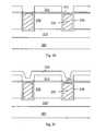
- the trenched DMOS device 100is supported on a substrate formed with an epitaxial drift layer 110 .
- the DMOS devicefurther includes a plurality of trenches opened in the epitaxial drift region 110 .
- the trenchesare padded with a gate oxide layer 115 and filled with a gate material, e.g., polysilicon 120 .
- Encompassed in the body regions 125are source regions 130 near the top surface of the epitaxial drift region 105 surrounding the trenched gates 120 .
- the source region 130is formed with a low barrier height metal to function as a silicide Schottky source.
- the gates 120is insulated further from the source region with a top insulation oxide layer 135 covered under an insulated spacer, e.g., silicon nitride spacers 140 , covering over the top oxide layer 135 .
- the DMOS device 100further includes a source contact trench opened in the body regions 125 above a body-contact dopant region 150 .
- the body-contact dopant regions 150are implanted and activation prior to the formation of the metal Schottky barrier 130 .
- the trenched contacts above the body contact dopant regions 150are formed through mask to etch through the metal silicide at body contact region. This configuration provides direct ohmic contact to the transistor body to reduce the transistor body resistance.
- a low resistance layer 155such as a layer of Ti/TiN is formed to cover the source contact to further increase the contact area to the source and body regions. Additionally, the metallization of silicide layer 130 as the source region achieves a significantly reduced contact resistance.
- the DMOS device 100further includes a metal contact layer 160 to function as a source metal and gate metal (not shown). An overlying passivation layer 170 further covers and protects the entire device.
- FIGS. 3A to 3 Vfor a serial of side cross sectional views to illustrate the fabrication steps of a DMOSFET device as that shown in FIG. 2 .
- a pad oxidationis carried out to form a pad oxide layer and a hard mask layer 215 is deposited to function as a hard mask.
- a trench mask(not shown) is applied to etch a plurality of trenches through the hard mask layer 215 and the epitaxial drift layer 210 supported on a substrate 205 .
- the trenchis oxidized with a sacrificial oxide to remove the plasma damaged silicon layer during the process of opening the trench.
- An oxidation processis performed to form an oxide layer 220 covering the trench walls as the gate oxide for the transistors.
- a polysilicon layer 225is deposited to fill the trench and covering the top surface and then doped with an N+ followed by applying a rapid thermal activation (RTA) process. Then the polysilicon layer is etched back as recessed trenched gate 225 surrounded by the hard mask layer 215 . A body dopant implant and diffusion are performed to form the body regions 230 .
- RTArapid thermal activation
- a gate annealing and gate oxidationforms an oxide layer 235 covering the polysilicon gate 225 .
- a silicon nitride spacer layer 240is deposited on top.
- SOGspin-on-glass
- a dry etch followed by a wet etch processare applied to remove the oxide hard mask 215 so that the mesa silicon surface is fully exposed.
- a blank isotropic silicon etchis performed on the silicon mesa surface.
- the polysilicon gate 225 recess in reference to the mesa silicon surfaceis reduced.
- Special caresare taken in the hard mask removal processes to assure sufficient gate oxide and poly-oxide layer thickness at the gate mesa corners to prevent weakness between the source and the gate.
- a contact mask 242is applied to implant contact dopant ions 244 to form body contact dopant region 245 .
- the contact mask 242is removed and cleaned.
- a rapid thermal activation (RTA) for the contact dopant region 245is carried out at a temperature around 900 to 950 C.
- FTplatinum
- FTlow barrier height rare earth metal layer 250
- silicidation process at low temperature of ⁇ 450 Cthat is well known in the art is carried out to form a low barrier height metal silicide layer, e.g., a PtSi layer 250 A.
- a low barrier height metal silicide layere.g., a PtSi layer 250 A.
- the un-reacted platinum or other low barrier height metalis removed.
- a contact mask 252is applied.
- a PtSi or other low barrier height metal silicide etchis carried out by applying an anisotropic etch with fluorine and chlorine gas mixture. The etch process can also be performed with a sputter etch with argon and oxygen gas mixture. Then a silicon etch is performed to open the contact opening 260 on top of the contact dopant region 245 . Then a cleaning process is performed to remove the surface damages and clean the photoresist 252 .
- a low resistance Ti/TiN layer 270is deposited on top followed by depositing a metal layer 280 on top.
- a metal maskis applied (not shown) to pattern the metal layer 270 into source metal and gate pad(s).
- a passivation layer 290is deposited on top to protect the device followed by applying a passivation mask (not shown) to pattern the passivation layer 290 to complete the manufacturing processes.
- This DMOS device 100 and the manufacturing methodovercome the disadvantages confronted by the conventional technologies.
- the processing steps of the DMOS device 100provide the trenched and recessed polysilicon gate, and furnishing the body contact implant and activation prior to the metal Schottky barrier formation. Therefore, all the high-temperature processing steps are completed before the metal source silicidation.
- the processing steps and configurationenable the employment of low-barrier height rare earth metal silicide for the best drive current.
- a trench contactis formulated through mask and etching of the metal silicide at body contact region, to form an ohmic contact to the transistor body.
- a metallizationis done to contact the whole mesa region (source and body contact), achieving low contact resistances.
- this inventiondiscloses a method for manufacturing a trenched semiconductor power device.
- the methodincludes a step of employing a low barrier-height rare earth metal for performing a metal source silicidation to form a source region surrounding a trenched gate of the semiconductor power device wherein the low barrier-height rare earth metal silicide having a barrier height in an approximate range of 0.20 to 0.35 eV to function as a Schottky source.
- the methodfurther includes a step of completing a plurality of high temperature processing steps before the step of metal source silicidation for enabling an employment of the a low barrier-height rare earth metal.
- the methodfurther includes a step of completing a plurality of high temperature processing steps including a step of formation of the trenched gate and furnishing a body contact implant and activation before the step of metal source silicidation for enabling an employment of the low barrier-height rare earth metal.
- FIG. 4shows a cross sectional view of an alternate preferred embodiment of a DMOS device 100 ′ this invention.
- the DMOS 100 ′has a similar device configuration as the DMOS 100 shown in FIG. 2 except that an insulation layer, e.g., a BPSG layer 145 is formed on top of the gate spacer 140 and the silicide source regions 130 to further insulate the gate from the source contact metal 160 .
- an insulation layere.g., a BPSG layer 145 is formed on top of the gate spacer 140 and the silicide source regions 130 to further insulate the gate from the source contact metal 160 .
- Such devicehas a further advantage to accommodate higher ratings in Vgs of the devices with the better insulation between gate and source metals.
- this inventiondiscloses a trenched semiconductor power device.
- the trenched semiconductor power deviceincludes a trenched gate insulated by a gate insulation layer and surrounded by a source region encompassed in a body region above a drain region disposed on a bottom surface of a semiconductor substrate.
- source region surrounding the trenched gateincludes a metal of low barrier height in an approximate range of 0.1 to 0.5 eV and preferably between 0.20 to 0.35 eV to function as a Schottky source.
- the metal of low barrier heightfurther includes a PtSi layer.
- the metal of low barrier heightfurther includes a ErSi layer.
- the metal of low barrier heightfurther includes a metal silicide layer having the low barrier height.
- the semiconductor power devicefurther includes a top insulation layer disposed under an insulation spacer on top of the trenched gate for insulating the trenched gate from the source region.
- the semiconductor power devicefurther includes a top oxide layer disposed under a silicon nitride spacer on top of the trenched gate for insulating the trenched gate from the source region.
- the semiconductor power devicefurther includes a source contact disposed in a trench opened into the body region for contacting a body-contact dopant region and covering with a conductive metal layer.
- the semiconductor power devicefurther includes a source contact trench opened into the body region for contacting a body-contact dopant region and covering with a Ti/TiN metal layer.
- the semiconductor power devicefurther includes a N-channel double diffusion metal oxide semiconductor (DMOS) device.
- the semiconductor power devicefurther includes a P-channel DMOS device.
- the semiconductor power devicefurther includes an asymmetrical double diffusion metal oxide semiconductor field effect transistor (DMOSFET) device. Its asymmetry arises from the fact that the source of the transistor is an Schottky metal silicide, yet the drain is of a silicon junction.
- DMOSFETasymmetrical double diffusion metal oxide semiconductor field effect transistor
Landscapes
- Engineering & Computer Science (AREA)
- Physics & Mathematics (AREA)
- Condensed Matter Physics & Semiconductors (AREA)
- General Physics & Mathematics (AREA)
- Manufacturing & Machinery (AREA)
- Computer Hardware Design (AREA)
- Microelectronics & Electronic Packaging (AREA)
- Power Engineering (AREA)
- Electrodes Of Semiconductors (AREA)
- Thin Film Transistor (AREA)
- Chemical & Material Sciences (AREA)
- Materials Engineering (AREA)
Abstract
Description
- 1. Field of the Invention
- The invention relates generally to the semiconductor power devices. More particularly, this invention relates to an improved and novel device manufacturing process to provide asymmetrical double diffusion metal oxide semiconductor field effect transistor (DMOSFET) with Schottky barrier source implemented with low-barrier height rare earth metal silicide for a best drive current without subject to a limitation of the high temperature processes and meanwhile providing low contact resistance of source and body contacts, which is achieved through silicided contact on the entire mesa area totally insulated from the trenched gates covered under an insulated spacer.
- 2. Description of the Prior Art
- It is known in the semiconductor power industry to implement a Schottky barrier source or metal silicide source electrode to overcome the parasitic bipolar conduction in a DMOSFET device. In order to prevent an unclamped inductor switching (UIS) in the semiconductor power device, it is necessary to reduce the parasitic bipolar conduction. With the implementation of Schottky barrier source the theoretical emitter efficiency at the source is reduced by orders of magnitude compared to the conventional silicon source junction structures. Such configuration can significantly eliminate the parasitic bipolar gain of the device. However, conventional manufacturing processes are still limited by the use of metals of high barrier height. The devices as now available to those of ordinary skill in the art therefore suffers low drive current and subject to potential increased body bias and reducing the gate drive or even forward bias the body-source junction and initiate a snapback.
- U.S. Pat. No. 4,675,713 discloses a method of using the source Schottky junction as the body contact for a semiconductor power device as shown in
FIG. 1A . The patented disclosure uses a low minority carrier injecting source region. A metal silicide layer is implemented to form the low minority carrier injection source region. The metal silicide source provides a source of majority carriers and meanwhile reducing the minority carrier injection and hence reducing the parasitic bipolar transistor action. However, the higher barrier height of the source contact can potentially increase the body bias and reduce the gate drive, or even increase the forward bias of the body-source junction and initiate a snapback. - U.S. Pat. No. 4,983,535 discloses a fabrication method to manufacture a DMOS device shown in
FIG. 1B . The method includes the processing steps use a starting material of a heavily doped silicon wafer, which has an epitaxial layer thereon. A DMOS body region is diffused into the epitaxial layer and a deep body contact region created. The source is a refractory metal Schottky barrier located on top of the body region. A trench is etched into the epitaxial layer so as to fully penetrate the body region and the trench surfaces oxidized to form a gate oxide. The trench is then filled with doped polysilicon to create a gate electrode. The resulting DMOS has a relatively short channel and the parallel bipolar parasitic transistor cannot be turned on. Since the method forms the Schottky barrier source prior to the trench and gate formation, therefore only refractory metal with high barrier height can be used. For this reasons, the device suffers a low drive current. - Therefore, a need still exists in the art of power semiconductor device design and manufacture to provide new manufacturing method and device configuration in forming the power devices such that the above discussed problems and limitations can be resolved.
- It is therefore an aspect of the present invention to provide a new and improved semiconductor power device implemented with a process of forming the trench and recessed poly gate, and furnishing the body contact implant and activation prior to the metal Schottky barrier formation. Therefore, all the high-temperature processing steps are done before the metal source silicidation. The new and improved manufacturing process enables the employment of low-barrier height rare earth metal silicide for the best drive current. The above-discussed difficulties as confronted by the conventional technologies are therefore resolved.
- Furthermore, this invention discloses a trench contact is formulated through mask and etching of the Schottky metal silicide at body contact region. This process provides a direct ohmic contact to the transistor body. Subsequent process steps eventually implement a metallization to contact the whole mesa region that includes the source and body contact. The metallization contact thus achieves a much-reduced contact resistance.
- Briefly in a preferred embodiment this invention discloses a trenched semiconductor power device comprising a trenched gate insulated by a gate insulation layer and surrounded by a source region encompassed in a body region above a drain region disposed on a bottom surface of a semiconductor substrate. The semiconductor power device further includes a source contact trench opened into the body region having a source contact dopant region disposed below and around sidewalls of the source contact trench to electrically contact the source region. The semiconductor power device further includes a source contact comprising a source contact conductive layer covering a bottom surface of the source contact trench contacting the source contact dopant region below the source contact trench wherein the source contact trench is further filled with an insulation material covering the conductive source contact layer. In a preferred embodiment, the semiconductor power device further includes a metal layer disposed under the insulation layer covering the source contact conductive layer for electrically contacting a top surface of the source region. In another preferred embodiment, the semiconductor power device further includes a silicide metal layer disposed under the insulation layer covering the source contact conductive layer for forming a salicided source conductive layer on the bottom surface of the source contact trench and the silicide metal layer further extending from the source contact trench for electrically contacting a top surface of the source region
- These and other objects and advantages of the present invention will no doubt become obvious to those of ordinary skill in the art after having read the following detailed description of the preferred embodiment, which is illustrated in the various drawing figures.
FIG. 1A is a cross sectional view of a conventional trenched MOSFET device implemented with a source contact by applying a metal with low barrier height.FIG. 1B shows another conventional semiconductor power deviceFIG. 2 is a cross sectional view of a trenched DMOS device as one exemplary embodiment of this invention.FIG. 3A to3K are a serial of cross sectional views for showing the manufacturing processes of a DMOS device of this invention as shown inFIG. 2 .FIG. 4 is a cross sectional view of a trenched DMOS device as another exemplary embodiment of this invention.- Referring to
FIG. 2 for a cross sectional view of a trenchedDMOS device 100. The trenchedDMOS device 100 is supported on a substrate formed with anepitaxial drift layer 110. The DMOS device further includes a plurality of trenches opened in theepitaxial drift region 110. The trenches are padded with agate oxide layer 115 and filled with a gate material, e.g.,polysilicon 120. Abody region 125 doped with a body dopant, e.g., P-type body dopant, surrounding the trenchedgates 120. Encompassed in thebody regions 125 aresource regions 130 near the top surface of theepitaxial drift region 105 surrounding thetrenched gates 120. Thesource region 130 is formed with a low barrier height metal to function as a silicide Schottky source. Thegates 120 is insulated further from the source region with a topinsulation oxide layer 135 covered under an insulated spacer, e.g.,silicon nitride spacers 140, covering over thetop oxide layer 135. - The
DMOS device 100 further includes a source contact trench opened in thebody regions 125 above a body-contact dopant region 150. As will be further described below, the body-contact dopant regions 150 are implanted and activation prior to the formation of themetal Schottky barrier 130. The trenched contacts above the bodycontact dopant regions 150 are formed through mask to etch through the metal silicide at body contact region. This configuration provides direct ohmic contact to the transistor body to reduce the transistor body resistance. - A
low resistance layer 155 such as a layer of Ti/TiN is formed to cover the source contact to further increase the contact area to the source and body regions. Additionally, the metallization ofsilicide layer 130 as the source region achieves a significantly reduced contact resistance. TheDMOS device 100 further includes ametal contact layer 160 to function as a source metal and gate metal (not shown). Anoverlying passivation layer 170 further covers and protects the entire device. - Referring to
FIGS. 3A to3V for a serial of side cross sectional views to illustrate the fabrication steps of a DMOSFET device as that shown inFIG. 2 . InFIG. 3A , a pad oxidation is carried out to form a pad oxide layer and ahard mask layer 215 is deposited to function as a hard mask. A trench mask (not shown) is applied to etch a plurality of trenches through thehard mask layer 215 and theepitaxial drift layer 210 supported on asubstrate 205. The trench is oxidized with a sacrificial oxide to remove the plasma damaged silicon layer during the process of opening the trench. An oxidation process is performed to form anoxide layer 220 covering the trench walls as the gate oxide for the transistors. Then apolysilicon layer 225 is deposited to fill the trench and covering the top surface and then doped with an N+ followed by applying a rapid thermal activation (RTA) process. Then the polysilicon layer is etched back as recessed trenchedgate 225 surrounded by thehard mask layer 215. A body dopant implant and diffusion are performed to form thebody regions 230. - In
FIG. 3B , a gate annealing and gate oxidation forms anoxide layer 235 covering thepolysilicon gate 225. InFIG. 3C , a siliconnitride spacer layer 240 is deposited on top. InFIG. 3D , either a photoresist (not shown) is applied or a spin-on-glass (SOG) is spanned on (not shown) and then blank etch back is done, removing thesilicon nitride layer 240 from the top of the hard mask leaving thespacer 240 around the side walls of thehard mask 215. Then the remaining photoresist or the SOG is removed with a cleaning process. InFIG. 3E , a dry etch followed by a wet etch process are applied to remove the oxidehard mask 215 so that the mesa silicon surface is fully exposed. A blank isotropic silicon etch is performed on the silicon mesa surface. Thepolysilicon gate 225 recess in reference to the mesa silicon surface is reduced. The source and gate overlap issues that could happen during the source silicidation process as will be further discussed below are mitigated. Special cares are taken in the hard mask removal processes to assure sufficient gate oxide and poly-oxide layer thickness at the gate mesa corners to prevent weakness between the source and the gate. - In
FIG. 3F , a contact mask242 is applied to implantcontact dopant ions 244 to form bodycontact dopant region 245. InFIG. 3G , the contact mask242 is removed and cleaned. A rapid thermal activation (RTA) for thecontact dopant region 245 is carried out at a temperature around 900 to 950 C. Then, a platinum (FT) or other low barrier height rareearth metal layer 250 is deposited. The thickness of themetal layer 250 is carefully optimized to obtain a good source and gate overlap after the source silicidation. InFIG. 3H , silicidation process at low temperature of ˜450 C that is well known in the art is carried out to form a low barrier height metal silicide layer, e.g., aPtSi layer 250A. The un-reacted platinum or other low barrier height metal is removed. - In
FIG. 3I , acontact mask 252 is applied. A PtSi or other low barrier height metal silicide etch is carried out by applying an anisotropic etch with fluorine and chlorine gas mixture. The etch process can also be performed with a sputter etch with argon and oxygen gas mixture. Then a silicon etch is performed to open thecontact opening 260 on top of thecontact dopant region 245. Then a cleaning process is performed to remove the surface damages and clean thephotoresist 252. InFIG. 3J , a low resistance Ti/TiN layer 270 is deposited on top followed by depositing ametal layer 280 on top. Then a metal mask is applied (not shown) to pattern themetal layer 270 into source metal and gate pad(s). InFIG. 3K , a passivation layer290 is deposited on top to protect the device followed by applying a passivation mask (not shown) to pattern the passivation layer290 to complete the manufacturing processes. - This
DMOS device 100 and the manufacturing method overcome the disadvantages confronted by the conventional technologies. The processing steps of theDMOS device 100 provide the trenched and recessed polysilicon gate, and furnishing the body contact implant and activation prior to the metal Schottky barrier formation. Therefore, all the high-temperature processing steps are completed before the metal source silicidation. The processing steps and configuration enable the employment of low-barrier height rare earth metal silicide for the best drive current. In the meantime, a trench contact is formulated through mask and etching of the metal silicide at body contact region, to form an ohmic contact to the transistor body. Eventually, a metallization is done to contact the whole mesa region (source and body contact), achieving low contact resistances. - According to
FIGS. 3A to3K and above descriptions, this invention discloses a method for manufacturing a trenched semiconductor power device. The method includes a step of employing a low barrier-height rare earth metal for performing a metal source silicidation to form a source region surrounding a trenched gate of the semiconductor power device wherein the low barrier-height rare earth metal silicide having a barrier height in an approximate range of 0.20 to 0.35 eV to function as a Schottky source. In a preferred embodiment, the method further includes a step of completing a plurality of high temperature processing steps before the step of metal source silicidation for enabling an employment of the a low barrier-height rare earth metal. In another preferred embodiment, the method further includes a step of completing a plurality of high temperature processing steps including a step of formation of the trenched gate and furnishing a body contact implant and activation before the step of metal source silicidation for enabling an employment of the low barrier-height rare earth metal. FIG. 4 shows a cross sectional view of an alternate preferred embodiment of aDMOS device 100′ this invention. TheDMOS 100′ has a similar device configuration as theDMOS 100 shown inFIG. 2 except that an insulation layer, e.g., aBPSG layer 145 is formed on top of thegate spacer 140 and thesilicide source regions 130 to further insulate the gate from thesource contact metal 160. Such device has a further advantage to accommodate higher ratings in Vgs of the devices with the better insulation between gate and source metals.- In a preferred embodiment, this invention discloses a trenched semiconductor power device. The trenched semiconductor power device includes a trenched gate insulated by a gate insulation layer and surrounded by a source region encompassed in a body region above a drain region disposed on a bottom surface of a semiconductor substrate. source region surrounding the trenched gate includes a metal of low barrier height in an approximate range of 0.1 to 0.5 eV and preferably between 0.20 to 0.35 eV to function as a Schottky source. In a preferred embodiment, the metal of low barrier height further includes a PtSi layer. In a preferred embodiment, the metal of low barrier height further includes a ErSi layer. In a preferred embodiment, the metal of low barrier height further includes a metal silicide layer having the low barrier height. In a preferred embodiment, the semiconductor power device further includes a top insulation layer disposed under an insulation spacer on top of the trenched gate for insulating the trenched gate from the source region. In a preferred embodiment, the semiconductor power device further includes a top oxide layer disposed under a silicon nitride spacer on top of the trenched gate for insulating the trenched gate from the source region. In a preferred embodiment, the semiconductor power device further includes a source contact disposed in a trench opened into the body region for contacting a body-contact dopant region and covering with a conductive metal layer. In a preferred embodiment, the semiconductor power device further includes a source contact trench opened into the body region for contacting a body-contact dopant region and covering with a Ti/TiN metal layer. In a preferred embodiment, the semiconductor power device further includes a N-channel double diffusion metal oxide semiconductor (DMOS) device. In a preferred embodiment, the semiconductor power device further includes a P-channel DMOS device. In a preferred embodiment, the semiconductor power device further includes an asymmetrical double diffusion metal oxide semiconductor field effect transistor (DMOSFET) device. Its asymmetry arises from the fact that the source of the transistor is an Schottky metal silicide, yet the drain is of a silicon junction.
- Although the present invention has been described in terms of the presently preferred embodiment, it is to be understood that such disclosure is not to be interpreted as limiting. Various alterations and modifications will no doubt become apparent to those skilled in the art after reading the above disclosure. Accordingly, it is intended that the appended claims be interpreted as covering all alterations and modifications as fall within the true spirit and scope of the invention.
Claims (25)
1. A trenched semiconductor power device comprising a trenched gate insulated by a gate insulation layer and surrounded by a source region encompassed in a body region above a drain region disposed on a bottom surface of a semiconductor substrate, wherein:
said source region surrounding said trenched gate comprising a metal of low barrier height in an approximate range of 0.1 to 0.5 eV to function as a Schottky source.
2. The trenched semiconductor power device ofclaim 1 wherein:
said metal of low barrier height further comprising a PtSi layer.
3. The trenched semiconductor power device ofclaim 1 wherein:
said metal of low barrier height further comprising a ErSi layer.
4. The trenched semiconductor power device ofclaim 1 wherein:
said metal of low barrier height further comprising a metal silicide layer having said low barrier height.
5. The trenched semiconductor power device ofclaim 1 further comprising:
a top gate insulation layer covered by an insulation spacer disposed on top of said trenched gate for insulating said trenched gate from said source region.
6. The trenched semiconductor power device ofclaim 1 further comprising:
a top oxide layer disposed under a silicon nitride spacer on top of said trenched gate for insulating said trenched gate from said source region.
7. The trenched semiconductor power device ofclaim 1 further comprising:
a source contact layer disposed on a bottom surface of a trench opened into said body region for contacting a body-contact dopant region and covering with a conductive metal layer.
8. The trenched semiconductor power device ofclaim 1 further comprising:
a source contact trench opened into said body region for contacting a body-contact dopant region and covering with a Ti/TiN metal layer.
9. The trenched semiconductor power device ofclaim 1 wherein:
said semiconductor power device further comprising a N-channel double diffusion metal oxide semiconductor (DMOS) device.
10. The trenched semiconductor power device ofclaim 1 wherein:
said semiconductor power device further comprising a P-channel DMOS device.
11. The trenched semiconductor power device ofclaim 1 wherein:
said semiconductor power device further comprising an asymmetrical double diffusion metal oxide semiconductor field effect transistor (DMOSFET) device.
12. The trenched semiconductor power device ofclaim 2 further comprising:
a top gate insulation layer covered by an insulation spacer disposed on top of said trenched gate for insulating said trenched gate from said source region; and
an insulation layer formed on top of said trenched gate spacer and said source region to further insulate the trenched gate from a source contact metal whereby said semiconductor power device is enabled to accommodate a higher rating of Vgs.
13. The trenched semiconductor power device ofclaim 1 further comprising:
a source contact trench opened into said body region and covering with a Ti/TiN metal layer for forming a salicided source contact trench contacting a body-contact dopant region disposed in said body region.
14. A trenched semiconductor power device comprising a trenched gate insulated by a gate insulation layer and surrounded by a source region encompassed in a body region above a drain region disposed on a bottom surface of a semiconductor substrate, said semiconductor power device further comprising:
a source contact trench opened into said body region having a source contact dopant region disposed below and around sidewalls of said source contact trench to electrically contact said source region; and
a source contact comprising a source contact conductive layer covering a bottom surface of said source contact trench contacting said source contact dopant region below said source contact trench wherein said source contact trench is further filled with an insulation material covering said conductive source contact layer.
15. The trenched semiconductor power device ofclaim 14 further comprising:
a metal layer disposed under said insulation layer covering said source contact conductive layer for electrically contacting a top surface of said source region.
16. The trenched semiconductor power device ofclaim 14 further comprising:
a silicide metal layer disposed under said insulation layer covering said source contact conductive layer for forming a salicided source conductive layer on said bottom surface of said source contact trench and said silicide metal layer further extending from said source contact trench for electrically contacting a top surface of said source region.
17. The trenched semiconductor power device ofclaim 14 wherein:
said source region surrounding said trenched gate comprising a metal of low barrier height in an approximate range of 0.1 to 0.5 eV to function as a Schottky source.
18. The trenched semiconductor power device ofclaim 17 wherein:
said metal of low barrier height further comprising a PtSi layer.
19. The trenched semiconductor power device ofclaim 17 wherein:
said metal of low barrier height further comprising an ErSi layer.
20. The trenched semiconductor power device ofclaim 17 wherein:
said metal of low barrier height further comprising a metal silicide layer having said low barrier height.
21. The trenched semiconductor power device ofclaim 14 further comprising:
a top gate insulation layer covered by an insulation spacer disposed on top of said trenched gate for insulating said trenched gate from said source region.
22. The trenched semiconductor power device ofclaim 14 further comprising:
a top oxide layer disposed under a silicon nitride spacer on top of said trenched gate for insulating said trenched gate from said source region.
23. A method for manufacturing a trenched semiconductor power device comprising:
employing a low barrier-height rare earth metal for performing a metal source silicidation to form a source region surrounding a trenched gate of said semiconductor power device wherein said low barrier-height rare earth metal silicide having a barrier height in an approximate range of 0.1 to 0.5 eV to function as a Schottky source.
24. The method ofclaim 23 further comprising:
completing a plurality of high temperature processing steps before said step of metal source silicidation for enabling an employment of said a low barrier-height rare earth metal.
25. The method ofclaim 23 further comprising:
completing a plurality of high temperature processing steps including a step of formation of said trenched gate and furnishing a body contact implant and activation before said step of metal source silicidation for enabling an employment of said a low barrier-height rare earth metal.
Priority Applications (2)
| Application Number | Priority Date | Filing Date | Title |
|---|---|---|---|
| US11/355,128US8022482B2 (en) | 2006-02-14 | 2006-02-14 | Device configuration of asymmetrical DMOSFET with schottky barrier source |
| US13/199,795US9337329B2 (en) | 2006-02-14 | 2011-09-08 | Method of fabrication and device configuration of asymmetrical DMOSFET with schottky barrier source |
Applications Claiming Priority (1)
| Application Number | Priority Date | Filing Date | Title |
|---|---|---|---|
| US11/355,128US8022482B2 (en) | 2006-02-14 | 2006-02-14 | Device configuration of asymmetrical DMOSFET with schottky barrier source |
Related Child Applications (1)
| Application Number | Title | Priority Date | Filing Date |
|---|---|---|---|
| US13/199,795DivisionUS9337329B2 (en) | 2006-02-14 | 2011-09-08 | Method of fabrication and device configuration of asymmetrical DMOSFET with schottky barrier source |
Publications (2)
| Publication Number | Publication Date |
|---|---|
| US20070187751A1true US20070187751A1 (en) | 2007-08-16 |
| US8022482B2 US8022482B2 (en) | 2011-09-20 |
Family
ID=38367494
Family Applications (2)
| Application Number | Title | Priority Date | Filing Date |
|---|---|---|---|
| US11/355,128Active2026-07-29US8022482B2 (en) | 2006-02-14 | 2006-02-14 | Device configuration of asymmetrical DMOSFET with schottky barrier source |
| US13/199,795Active2028-12-12US9337329B2 (en) | 2006-02-14 | 2011-09-08 | Method of fabrication and device configuration of asymmetrical DMOSFET with schottky barrier source |
Family Applications After (1)
| Application Number | Title | Priority Date | Filing Date |
|---|---|---|---|
| US13/199,795Active2028-12-12US9337329B2 (en) | 2006-02-14 | 2011-09-08 | Method of fabrication and device configuration of asymmetrical DMOSFET with schottky barrier source |
Country Status (1)
| Country | Link |
|---|---|
| US (2) | US8022482B2 (en) |
Cited By (51)
| Publication number | Priority date | Publication date | Assignee | Title |
|---|---|---|---|---|
| US20080265396A1 (en)* | 2006-05-23 | 2008-10-30 | International Business Machines Corporation | Quad flat no-lead chip carrier with standoff |
| US20090080244A1 (en)* | 2007-09-17 | 2009-03-26 | Eric Carman | Refreshing Data of Memory Cells with Electrically Floating Body Transistors |
| US20090140323A1 (en)* | 2007-11-29 | 2009-06-04 | Pierre Fazan | Integrated Circuit having Memory Cell Array including Barriers, and Method of Manufacturing Same |
| US20100085806A1 (en)* | 2008-10-02 | 2010-04-08 | Ping Wang | Techniques for reducing a voltage swing |
| US20100224924A1 (en)* | 2009-03-04 | 2010-09-09 | Innovative Silicon Isi Sa | Techniques for forming a contact to a buried diffusion layer in a semiconductor memory device |
| US7924630B2 (en) | 2008-10-15 | 2011-04-12 | Micron Technology, Inc. | Techniques for simultaneously driving a plurality of source lines |
| US7933142B2 (en) | 2006-05-02 | 2011-04-26 | Micron Technology, Inc. | Semiconductor memory cell and array using punch-through to program and read same |
| US7940559B2 (en) | 2006-04-07 | 2011-05-10 | Micron Technology, Inc. | Memory array having a programmable word length, and method of operating same |
| US7947543B2 (en) | 2008-09-25 | 2011-05-24 | Micron Technology, Inc. | Recessed gate silicon-on-insulator floating body device with self-aligned lateral isolation |
| US7957206B2 (en) | 2008-04-04 | 2011-06-07 | Micron Technology, Inc. | Read circuitry for an integrated circuit having memory cells and/or a memory cell array, and method of operating same |
| US20110133258A1 (en)* | 2009-08-14 | 2011-06-09 | Alpha And Omega Semiconductor Incorporated | Shielded gate trench mosfet with increased source-metal contact |
| US8014195B2 (en) | 2008-02-06 | 2011-09-06 | Micron Technology, Inc. | Single transistor memory cell |
| US8064274B2 (en) | 2007-05-30 | 2011-11-22 | Micron Technology, Inc. | Integrated circuit having voltage generation circuitry for memory cell array, and method of operating and/or controlling same |
| US8069377B2 (en) | 2006-06-26 | 2011-11-29 | Micron Technology, Inc. | Integrated circuit having memory array including ECC and column redundancy and method of operating the same |
| US8085594B2 (en) | 2007-06-01 | 2011-12-27 | Micron Technology, Inc. | Reading technique for memory cell with electrically floating body transistor |
| US8139418B2 (en) | 2009-04-27 | 2012-03-20 | Micron Technology, Inc. | Techniques for controlling a direct injection semiconductor memory device |
| US8174881B2 (en) | 2009-11-24 | 2012-05-08 | Micron Technology, Inc. | Techniques for reducing disturbance in a semiconductor device |
| US8189376B2 (en) | 2008-02-08 | 2012-05-29 | Micron Technology, Inc. | Integrated circuit having memory cells including gate material having high work function, and method of manufacturing same |
| US8199595B2 (en) | 2009-09-04 | 2012-06-12 | Micron Technology, Inc. | Techniques for sensing a semiconductor memory device |
| US8213226B2 (en) | 2008-12-05 | 2012-07-03 | Micron Technology, Inc. | Vertical transistor memory cell and array |
| US8223574B2 (en) | 2008-11-05 | 2012-07-17 | Micron Technology, Inc. | Techniques for block refreshing a semiconductor memory device |
| US20120205737A1 (en)* | 2009-08-14 | 2012-08-16 | Alpha And Omega Semiconductor Inc | Shielded gate trench mosfet device and fabrication |
| US8264041B2 (en) | 2007-01-26 | 2012-09-11 | Micron Technology, Inc. | Semiconductor device with electrically floating body |
| US8310893B2 (en) | 2009-12-16 | 2012-11-13 | Micron Technology, Inc. | Techniques for reducing impact of array disturbs in a semiconductor memory device |
| US8315099B2 (en) | 2009-07-27 | 2012-11-20 | Micron Technology, Inc. | Techniques for providing a direct injection semiconductor memory device |
| US8319294B2 (en) | 2009-02-18 | 2012-11-27 | Micron Technology, Inc. | Techniques for providing a source line plane |
| US8349662B2 (en) | 2007-12-11 | 2013-01-08 | Micron Technology, Inc. | Integrated circuit having memory cell array, and method of manufacturing same |
| US8369177B2 (en) | 2010-03-05 | 2013-02-05 | Micron Technology, Inc. | Techniques for reading from and/or writing to a semiconductor memory device |
| US8411524B2 (en) | 2010-05-06 | 2013-04-02 | Micron Technology, Inc. | Techniques for refreshing a semiconductor memory device |
| US8411513B2 (en) | 2010-03-04 | 2013-04-02 | Micron Technology, Inc. | Techniques for providing a semiconductor memory device having hierarchical bit lines |
| US8416636B2 (en) | 2010-02-12 | 2013-04-09 | Micron Technology, Inc. | Techniques for controlling a semiconductor memory device |
| US20130153926A1 (en)* | 2011-12-20 | 2013-06-20 | Sumitomo Electric Industries, Ltd. | Semiconductor device and method for manufacturing same |
| US8498157B2 (en) | 2009-05-22 | 2013-07-30 | Micron Technology, Inc. | Techniques for providing a direct injection semiconductor memory device |
| US8508994B2 (en) | 2009-04-30 | 2013-08-13 | Micron Technology, Inc. | Semiconductor device with floating gate and electrically floating body |
| US20130214417A1 (en)* | 2012-02-21 | 2013-08-22 | Micron Technology, Inc. | Methods of forming a metal silicide region on at least one silicon structure |
| US8518774B2 (en) | 2007-03-29 | 2013-08-27 | Micron Technology, Inc. | Manufacturing process for zero-capacitor random access memory circuits |
| US8531878B2 (en) | 2011-05-17 | 2013-09-10 | Micron Technology, Inc. | Techniques for providing a semiconductor memory device |
| US8537610B2 (en) | 2009-07-10 | 2013-09-17 | Micron Technology, Inc. | Techniques for providing a semiconductor memory device |
| US8547738B2 (en) | 2010-03-15 | 2013-10-01 | Micron Technology, Inc. | Techniques for providing a semiconductor memory device |
| US8576631B2 (en) | 2010-03-04 | 2013-11-05 | Micron Technology, Inc. | Techniques for sensing a semiconductor memory device |
| CN103515444A (en)* | 2013-09-24 | 2014-01-15 | 哈尔滨工程大学 | Groove gate power MOS device |
| CN103531628A (en)* | 2012-07-02 | 2014-01-22 | 朱江 | Groove Schottky MOS semiconductor device and preparation method thereof |
| US8748959B2 (en) | 2009-03-31 | 2014-06-10 | Micron Technology, Inc. | Semiconductor memory device |
| US8773933B2 (en) | 2012-03-16 | 2014-07-08 | Micron Technology, Inc. | Techniques for accessing memory cells |
| US8873283B2 (en) | 2005-09-07 | 2014-10-28 | Micron Technology, Inc. | Memory cell and memory cell array having an electrically floating body transistor, and methods of operating same |
| US9099553B2 (en) | 2012-01-13 | 2015-08-04 | Sumitomo Electric Industries, Ltd. | Semiconductor device and method for manufacturing same |
| US20150221764A1 (en)* | 2014-02-04 | 2015-08-06 | Infineon Technologies Ag | Wafer based beol process for chip embedding |
| US9559216B2 (en) | 2011-06-06 | 2017-01-31 | Micron Technology, Inc. | Semiconductor memory device and method for biasing same |
| CN108777257A (en)* | 2014-06-06 | 2018-11-09 | 意法半导体公司 | Backside source-drain contact and preparation method thereof for integrated circuit transistor device |
| CN113097126A (en)* | 2020-01-09 | 2021-07-09 | 珠海格力电器股份有限公司 | Chip, power device and manufacturing method of chip |
| CN113793873A (en)* | 2021-09-17 | 2021-12-14 | 江苏格瑞宝电子有限公司 | P-type MOSFET structure with metal layer as source region and preparation method thereof |
Families Citing this family (9)
| Publication number | Priority date | Publication date | Assignee | Title |
|---|---|---|---|---|
| JP5222466B2 (en) | 2006-08-09 | 2013-06-26 | ルネサスエレクトロニクス株式会社 | Semiconductor device and manufacturing method thereof |
| US8610235B2 (en) | 2011-09-22 | 2013-12-17 | Alpha And Omega Semiconductor Incorporated | Trench MOSFET with integrated Schottky barrier diode |
| US9385228B2 (en) | 2013-11-27 | 2016-07-05 | Infineon Technologies Ag | Semiconductor device with cell trench structures and contacts and method of manufacturing a semiconductor device |
| US10510869B2 (en) | 2016-05-06 | 2019-12-17 | Silicet, LLC | Devices and methods for a power transistor having a Schottky or Schottky-like contact |
| US9947787B2 (en) | 2016-05-06 | 2018-04-17 | Silicet, LLC | Devices and methods for a power transistor having a schottky or schottky-like contact |
| US10714580B2 (en)* | 2018-02-07 | 2020-07-14 | Alpha And Omega Semiconductor (Cayman) Ltd. | Source ballasting for p-channel trench MOSFET |
| US11228174B1 (en) | 2019-05-30 | 2022-01-18 | Silicet, LLC | Source and drain enabled conduction triggers and immunity tolerance for integrated circuits |
| US10892362B1 (en) | 2019-11-06 | 2021-01-12 | Silicet, LLC | Devices for LDMOS and other MOS transistors with hybrid contact |
| WO2022120175A1 (en) | 2020-12-04 | 2022-06-09 | Amplexia, Llc | Ldmos with self-aligned body and hybrid source |
Citations (14)
| Publication number | Priority date | Publication date | Assignee | Title |
|---|---|---|---|---|
| US4675713A (en)* | 1982-05-10 | 1987-06-23 | Motorola, Inc. | MOS transistor |
| US4983535A (en)* | 1981-10-15 | 1991-01-08 | Siliconix Incorporated | Vertical DMOS transistor fabrication process |
| US20020115257A1 (en)* | 2001-02-19 | 2002-08-22 | Hitachi, Ltd. | Insulated gate type semiconductor device and method for fabricating the same |
| US20030001215A1 (en)* | 2001-10-02 | 2003-01-02 | Fraunhofer-Gesellschaft Zur Foerderung Derangewandten Forschung E.V. | Power MOS element and method for producing the same |
| US20030060013A1 (en)* | 1999-09-24 | 2003-03-27 | Bruce D. Marchant | Method of manufacturing trench field effect transistors with trenched heavy body |
| US6621107B2 (en)* | 2001-08-23 | 2003-09-16 | General Semiconductor, Inc. | Trench DMOS transistor with embedded trench schottky rectifier |
| US20040021174A1 (en)* | 2002-04-24 | 2004-02-05 | Kenya Kobayashi | Vertical MOSFET reduced in cell size and method of producing the same |
| US7081388B2 (en)* | 2004-03-01 | 2006-07-25 | International Rectifier Corporation | Self aligned contact structure for trench device |
| US20060273384A1 (en)* | 2005-06-06 | 2006-12-07 | M-Mos Sdn. Bhd. | Structure for avalanche improvement of ultra high density trench MOSFET |
| US20060273380A1 (en)* | 2005-06-06 | 2006-12-07 | M-Mos Sdn.Bhd. | Source contact and metal scheme for high density trench MOSFET |
| US7166891B2 (en)* | 2003-10-01 | 2007-01-23 | Rohm Co., Ltd. | Semiconductor device with etch resistant electrical insulation layer between gate electrode and source electrode |
| US20070075362A1 (en)* | 2005-09-30 | 2007-04-05 | Ching-Yuan Wu | Self-aligned schottky-barrier clamped trench DMOS transistor structure and its manufacturing methods |
| US7214576B1 (en)* | 2005-09-08 | 2007-05-08 | Kabushiki Kaisha Toshiba | Manufacturing method of semiconductor device |
| US7504690B2 (en)* | 2002-10-04 | 2009-03-17 | Nxp B.V. | Power semiconductor devices |
Family Cites Families (3)
| Publication number | Priority date | Publication date | Assignee | Title |
|---|---|---|---|---|
| JP2004055803A (en)* | 2002-07-19 | 2004-02-19 | Renesas Technology Corp | Semiconductor device |
| US6861701B2 (en)* | 2003-03-05 | 2005-03-01 | Advanced Analogic Technologies, Inc. | Trench power MOSFET with planarized gate bus |
| CN101019236A (en)* | 2004-07-15 | 2007-08-15 | 斯平内克半导体股份有限公司 | Metal source power transistor and method of manufacture |
- 2006
- 2006-02-14USUS11/355,128patent/US8022482B2/enactiveActive
- 2011
- 2011-09-08USUS13/199,795patent/US9337329B2/enactiveActive
Patent Citations (14)
| Publication number | Priority date | Publication date | Assignee | Title |
|---|---|---|---|---|
| US4983535A (en)* | 1981-10-15 | 1991-01-08 | Siliconix Incorporated | Vertical DMOS transistor fabrication process |
| US4675713A (en)* | 1982-05-10 | 1987-06-23 | Motorola, Inc. | MOS transistor |
| US20030060013A1 (en)* | 1999-09-24 | 2003-03-27 | Bruce D. Marchant | Method of manufacturing trench field effect transistors with trenched heavy body |
| US20020115257A1 (en)* | 2001-02-19 | 2002-08-22 | Hitachi, Ltd. | Insulated gate type semiconductor device and method for fabricating the same |
| US6621107B2 (en)* | 2001-08-23 | 2003-09-16 | General Semiconductor, Inc. | Trench DMOS transistor with embedded trench schottky rectifier |
| US20030001215A1 (en)* | 2001-10-02 | 2003-01-02 | Fraunhofer-Gesellschaft Zur Foerderung Derangewandten Forschung E.V. | Power MOS element and method for producing the same |
| US20040021174A1 (en)* | 2002-04-24 | 2004-02-05 | Kenya Kobayashi | Vertical MOSFET reduced in cell size and method of producing the same |
| US7504690B2 (en)* | 2002-10-04 | 2009-03-17 | Nxp B.V. | Power semiconductor devices |
| US7166891B2 (en)* | 2003-10-01 | 2007-01-23 | Rohm Co., Ltd. | Semiconductor device with etch resistant electrical insulation layer between gate electrode and source electrode |
| US7081388B2 (en)* | 2004-03-01 | 2006-07-25 | International Rectifier Corporation | Self aligned contact structure for trench device |
| US20060273384A1 (en)* | 2005-06-06 | 2006-12-07 | M-Mos Sdn. Bhd. | Structure for avalanche improvement of ultra high density trench MOSFET |
| US20060273380A1 (en)* | 2005-06-06 | 2006-12-07 | M-Mos Sdn.Bhd. | Source contact and metal scheme for high density trench MOSFET |
| US7214576B1 (en)* | 2005-09-08 | 2007-05-08 | Kabushiki Kaisha Toshiba | Manufacturing method of semiconductor device |
| US20070075362A1 (en)* | 2005-09-30 | 2007-04-05 | Ching-Yuan Wu | Self-aligned schottky-barrier clamped trench DMOS transistor structure and its manufacturing methods |
Cited By (109)
| Publication number | Priority date | Publication date | Assignee | Title |
|---|---|---|---|---|
| US11031069B2 (en) | 2005-09-07 | 2021-06-08 | Ovonyx Memory Technology, Llc | Memory cell and memory cell array having an electrically floating body transistor, and methods of operating same |
| US10418091B2 (en) | 2005-09-07 | 2019-09-17 | Ovonyx Memory Technology, Llc | Memory cell and memory cell array having an electrically floating body transistor, and methods of operating same |
| US8873283B2 (en) | 2005-09-07 | 2014-10-28 | Micron Technology, Inc. | Memory cell and memory cell array having an electrically floating body transistor, and methods of operating same |
| US7940559B2 (en) | 2006-04-07 | 2011-05-10 | Micron Technology, Inc. | Memory array having a programmable word length, and method of operating same |
| US8134867B2 (en) | 2006-04-07 | 2012-03-13 | Micron Technology, Inc. | Memory array having a programmable word length, and method of operating same |
| US8295078B2 (en) | 2006-05-02 | 2012-10-23 | Micron Technology, Inc. | Semiconductor memory cell and array using punch-through to program and read same |
| US7933142B2 (en) | 2006-05-02 | 2011-04-26 | Micron Technology, Inc. | Semiconductor memory cell and array using punch-through to program and read same |
| US20080265396A1 (en)* | 2006-05-23 | 2008-10-30 | International Business Machines Corporation | Quad flat no-lead chip carrier with standoff |
| US8402326B2 (en) | 2006-06-26 | 2013-03-19 | Micron Technology, Inc. | Integrated circuit having memory array including ECC and column redundancy and method of operating same |
| US8069377B2 (en) | 2006-06-26 | 2011-11-29 | Micron Technology, Inc. | Integrated circuit having memory array including ECC and column redundancy and method of operating the same |
| US8492209B2 (en) | 2007-01-26 | 2013-07-23 | Micron Technology, Inc. | Semiconductor device with electrically floating body |
| US8796770B2 (en) | 2007-01-26 | 2014-08-05 | Micron Technology, Inc. | Semiconductor device with electrically floating body |
| US8264041B2 (en) | 2007-01-26 | 2012-09-11 | Micron Technology, Inc. | Semiconductor device with electrically floating body |
| US8518774B2 (en) | 2007-03-29 | 2013-08-27 | Micron Technology, Inc. | Manufacturing process for zero-capacitor random access memory circuits |
| US9276000B2 (en) | 2007-03-29 | 2016-03-01 | Micron Technology, Inc. | Manufacturing process for zero-capacitor random access memory circuits |
| US8064274B2 (en) | 2007-05-30 | 2011-11-22 | Micron Technology, Inc. | Integrated circuit having voltage generation circuitry for memory cell array, and method of operating and/or controlling same |
| US9257155B2 (en) | 2007-05-30 | 2016-02-09 | Micron Technology, Inc. | Integrated circuit having voltage generation circuitry for memory cell array, and method of operating and/or controlling same |
| US8659956B2 (en) | 2007-05-30 | 2014-02-25 | Micron Technology, Inc. | Integrated circuit having voltage generation circuitry for memory cell array, and method of operating and/or controlling same |
| US8659948B2 (en) | 2007-06-01 | 2014-02-25 | Micron Technology, Inc. | Techniques for reading a memory cell with electrically floating body transistor |
| US8085594B2 (en) | 2007-06-01 | 2011-12-27 | Micron Technology, Inc. | Reading technique for memory cell with electrically floating body transistor |
| US20090080244A1 (en)* | 2007-09-17 | 2009-03-26 | Eric Carman | Refreshing Data of Memory Cells with Electrically Floating Body Transistors |
| US8194487B2 (en) | 2007-09-17 | 2012-06-05 | Micron Technology, Inc. | Refreshing data of memory cells with electrically floating body transistors |
| US8797819B2 (en) | 2007-09-17 | 2014-08-05 | Micron Technology, Inc. | Refreshing data of memory cells with electrically floating body transistors |
| US8446794B2 (en) | 2007-09-17 | 2013-05-21 | Micron Technology, Inc. | Refreshing data of memory cells with electrically floating body transistors |
| US11081486B2 (en) | 2007-11-29 | 2021-08-03 | Ovonyx Memory Technology, Llc | Integrated circuit having memory cell array including barriers, and method of manufacturing same |
| US10304837B2 (en) | 2007-11-29 | 2019-05-28 | Ovonyx Memory Technology, Llc | Integrated circuit having memory cell array including barriers, and method of manufacturing same |
| US8536628B2 (en) | 2007-11-29 | 2013-09-17 | Micron Technology, Inc. | Integrated circuit having memory cell array including barriers, and method of manufacturing same |
| WO2009068548A1 (en)* | 2007-11-29 | 2009-06-04 | Innovative Silicon Isi Sa | Integrated circuit having memory cell array including barriers, and method of manufacturing same |
| US20090140323A1 (en)* | 2007-11-29 | 2009-06-04 | Pierre Fazan | Integrated Circuit having Memory Cell Array including Barriers, and Method of Manufacturing Same |
| US8349662B2 (en) | 2007-12-11 | 2013-01-08 | Micron Technology, Inc. | Integrated circuit having memory cell array, and method of manufacturing same |
| US9019788B2 (en) | 2008-01-24 | 2015-04-28 | Micron Technology, Inc. | Techniques for accessing memory cells |
| US8325515B2 (en) | 2008-02-06 | 2012-12-04 | Micron Technology, Inc. | Integrated circuit device |
| US8014195B2 (en) | 2008-02-06 | 2011-09-06 | Micron Technology, Inc. | Single transistor memory cell |
| US8189376B2 (en) | 2008-02-08 | 2012-05-29 | Micron Technology, Inc. | Integrated circuit having memory cells including gate material having high work function, and method of manufacturing same |
| US8274849B2 (en) | 2008-04-04 | 2012-09-25 | Micron Technology, Inc. | Read circuitry for an integrated circuit having memory cells and/or a memory cell array, and method of operating same |
| US7957206B2 (en) | 2008-04-04 | 2011-06-07 | Micron Technology, Inc. | Read circuitry for an integrated circuit having memory cells and/or a memory cell array, and method of operating same |
| US8790968B2 (en) | 2008-09-25 | 2014-07-29 | Micron Technology, Inc. | Recessed gate silicon-on-insulator floating body device with self-aligned lateral isolation |
| US9553186B2 (en) | 2008-09-25 | 2017-01-24 | Micron Technology, Inc. | Recessed gate silicon-on-insulator floating body device with self-aligned lateral isolation |
| US7947543B2 (en) | 2008-09-25 | 2011-05-24 | Micron Technology, Inc. | Recessed gate silicon-on-insulator floating body device with self-aligned lateral isolation |
| US7933140B2 (en) | 2008-10-02 | 2011-04-26 | Micron Technology, Inc. | Techniques for reducing a voltage swing |
| US20100085806A1 (en)* | 2008-10-02 | 2010-04-08 | Ping Wang | Techniques for reducing a voltage swing |
| US8315083B2 (en) | 2008-10-02 | 2012-11-20 | Micron Technology Inc. | Techniques for reducing a voltage swing |
| US7924630B2 (en) | 2008-10-15 | 2011-04-12 | Micron Technology, Inc. | Techniques for simultaneously driving a plurality of source lines |
| US8223574B2 (en) | 2008-11-05 | 2012-07-17 | Micron Technology, Inc. | Techniques for block refreshing a semiconductor memory device |
| US8213226B2 (en) | 2008-12-05 | 2012-07-03 | Micron Technology, Inc. | Vertical transistor memory cell and array |
| US8319294B2 (en) | 2009-02-18 | 2012-11-27 | Micron Technology, Inc. | Techniques for providing a source line plane |
| US20100224924A1 (en)* | 2009-03-04 | 2010-09-09 | Innovative Silicon Isi Sa | Techniques for forming a contact to a buried diffusion layer in a semiconductor memory device |
| US9064730B2 (en) | 2009-03-04 | 2015-06-23 | Micron Technology, Inc. | Techniques for forming a contact to a buried diffusion layer in a semiconductor memory device |
| US8710566B2 (en) | 2009-03-04 | 2014-04-29 | Micron Technology, Inc. | Techniques for forming a contact to a buried diffusion layer in a semiconductor memory device |
| US9093311B2 (en) | 2009-03-31 | 2015-07-28 | Micron Technology, Inc. | Techniques for providing a semiconductor memory device |
| US8748959B2 (en) | 2009-03-31 | 2014-06-10 | Micron Technology, Inc. | Semiconductor memory device |
| US8139418B2 (en) | 2009-04-27 | 2012-03-20 | Micron Technology, Inc. | Techniques for controlling a direct injection semiconductor memory device |
| US8861247B2 (en) | 2009-04-27 | 2014-10-14 | Micron Technology, Inc. | Techniques for providing a direct injection semiconductor memory device |
| US8508970B2 (en) | 2009-04-27 | 2013-08-13 | Micron Technology, Inc. | Techniques for providing a direct injection semiconductor memory device |
| US8400811B2 (en) | 2009-04-27 | 2013-03-19 | Micron Technology, Inc. | Techniques for providing a direct injection semiconductor memory device having ganged carrier injection lines |
| US8351266B2 (en) | 2009-04-27 | 2013-01-08 | Micron Technology, Inc. | Techniques for controlling a direct injection semiconductor memory device |
| US9425190B2 (en) | 2009-04-27 | 2016-08-23 | Micron Technology, Inc. | Techniques for providing a direct injection semiconductor memory device |
| US8508994B2 (en) | 2009-04-30 | 2013-08-13 | Micron Technology, Inc. | Semiconductor device with floating gate and electrically floating body |
| US8792276B2 (en) | 2009-04-30 | 2014-07-29 | Micron Technology, Inc. | Semiconductor device with floating gate and electrically floating body |
| US9240496B2 (en) | 2009-04-30 | 2016-01-19 | Micron Technology, Inc. | Semiconductor device with floating gate and electrically floating body |
| US8982633B2 (en) | 2009-05-22 | 2015-03-17 | Micron Technology, Inc. | Techniques for providing a direct injection semiconductor memory device |
| US8498157B2 (en) | 2009-05-22 | 2013-07-30 | Micron Technology, Inc. | Techniques for providing a direct injection semiconductor memory device |
| US8817534B2 (en) | 2009-07-10 | 2014-08-26 | Micron Technology, Inc. | Techniques for providing a semiconductor memory device |
| US9331083B2 (en) | 2009-07-10 | 2016-05-03 | Micron Technology, Inc. | Techniques for providing a semiconductor memory device |
| US8537610B2 (en) | 2009-07-10 | 2013-09-17 | Micron Technology, Inc. | Techniques for providing a semiconductor memory device |
| US9076543B2 (en) | 2009-07-27 | 2015-07-07 | Micron Technology, Inc. | Techniques for providing a direct injection semiconductor memory device |
| US8964461B2 (en) | 2009-07-27 | 2015-02-24 | Micron Technology, Inc. | Techniques for providing a direct injection semiconductor memory device |
| US8947965B2 (en) | 2009-07-27 | 2015-02-03 | Micron Technology Inc. | Techniques for providing a direct injection semiconductor memory device |
| US8315099B2 (en) | 2009-07-27 | 2012-11-20 | Micron Technology, Inc. | Techniques for providing a direct injection semiconductor memory device |
| US8587996B2 (en) | 2009-07-27 | 2013-11-19 | Micron Technology, Inc. | Techniques for providing a direct injection semiconductor memory device |
| US9679612B2 (en) | 2009-07-27 | 2017-06-13 | Micron Technology, Inc. | Techniques for providing a direct injection semiconductor memory device |
| US8618601B2 (en) | 2009-08-14 | 2013-12-31 | Alpha And Omega Semiconductor Incorporated | Shielded gate trench MOSFET with increased source-metal contact |
| US8564055B2 (en)* | 2009-08-14 | 2013-10-22 | Alpha And Omega Semiconductor Incorporated | Shielded gate trench MOSFET device and fabrication |
| US20120205737A1 (en)* | 2009-08-14 | 2012-08-16 | Alpha And Omega Semiconductor Inc | Shielded gate trench mosfet device and fabrication |
| US10680097B2 (en) | 2009-08-14 | 2020-06-09 | Alpha And Omega Semiconductor Incorporated | MOSFET device and fabrication |
| US20110133258A1 (en)* | 2009-08-14 | 2011-06-09 | Alpha And Omega Semiconductor Incorporated | Shielded gate trench mosfet with increased source-metal contact |
| US8199595B2 (en) | 2009-09-04 | 2012-06-12 | Micron Technology, Inc. | Techniques for sensing a semiconductor memory device |
| US9812179B2 (en) | 2009-11-24 | 2017-11-07 | Ovonyx Memory Technology, Llc | Techniques for reducing disturbance in a semiconductor memory device |
| US8760906B2 (en) | 2009-11-24 | 2014-06-24 | Micron Technology, Inc. | Techniques for reducing disturbance in a semiconductor memory device |
| US8699289B2 (en) | 2009-11-24 | 2014-04-15 | Micron Technology, Inc. | Techniques for reducing disturbance in a semiconductor memory device |
| US8174881B2 (en) | 2009-11-24 | 2012-05-08 | Micron Technology, Inc. | Techniques for reducing disturbance in a semiconductor device |
| US8310893B2 (en) | 2009-12-16 | 2012-11-13 | Micron Technology, Inc. | Techniques for reducing impact of array disturbs in a semiconductor memory device |
| US8416636B2 (en) | 2010-02-12 | 2013-04-09 | Micron Technology, Inc. | Techniques for controlling a semiconductor memory device |
| US8411513B2 (en) | 2010-03-04 | 2013-04-02 | Micron Technology, Inc. | Techniques for providing a semiconductor memory device having hierarchical bit lines |
| US8576631B2 (en) | 2010-03-04 | 2013-11-05 | Micron Technology, Inc. | Techniques for sensing a semiconductor memory device |
| US8964479B2 (en) | 2010-03-04 | 2015-02-24 | Micron Technology, Inc. | Techniques for sensing a semiconductor memory device |
| US8369177B2 (en) | 2010-03-05 | 2013-02-05 | Micron Technology, Inc. | Techniques for reading from and/or writing to a semiconductor memory device |
| US8547738B2 (en) | 2010-03-15 | 2013-10-01 | Micron Technology, Inc. | Techniques for providing a semiconductor memory device |
| US9019759B2 (en) | 2010-03-15 | 2015-04-28 | Micron Technology, Inc. | Techniques for providing a semiconductor memory device |
| US9524971B2 (en) | 2010-03-15 | 2016-12-20 | Micron Technology, Inc. | Techniques for providing a semiconductor memory device |
| US8630126B2 (en) | 2010-05-06 | 2014-01-14 | Micron Technology, Inc. | Techniques for refreshing a semiconductor memory device |
| US8411524B2 (en) | 2010-05-06 | 2013-04-02 | Micron Technology, Inc. | Techniques for refreshing a semiconductor memory device |
| US9142264B2 (en) | 2010-05-06 | 2015-09-22 | Micron Technology, Inc. | Techniques for refreshing a semiconductor memory device |
| US9263133B2 (en) | 2011-05-17 | 2016-02-16 | Micron Technology, Inc. | Techniques for providing a semiconductor memory device |
| US8531878B2 (en) | 2011-05-17 | 2013-09-10 | Micron Technology, Inc. | Techniques for providing a semiconductor memory device |
| US9559216B2 (en) | 2011-06-06 | 2017-01-31 | Micron Technology, Inc. | Semiconductor memory device and method for biasing same |
| US20130153926A1 (en)* | 2011-12-20 | 2013-06-20 | Sumitomo Electric Industries, Ltd. | Semiconductor device and method for manufacturing same |
| US8829605B2 (en)* | 2011-12-20 | 2014-09-09 | Sumitomo Electric Industries, Ltd. | Semiconductor device having deep and shallow trenches |
| US9099553B2 (en) | 2012-01-13 | 2015-08-04 | Sumitomo Electric Industries, Ltd. | Semiconductor device and method for manufacturing same |
| US20130214417A1 (en)* | 2012-02-21 | 2013-08-22 | Micron Technology, Inc. | Methods of forming a metal silicide region on at least one silicon structure |
| US9224807B2 (en) | 2012-02-21 | 2015-12-29 | Micron Technology, Inc. | Arrays of silicon structures including metal silicide regions, and related semiconductor device structures |
| US8692373B2 (en)* | 2012-02-21 | 2014-04-08 | Micron Technology, Inc. | Methods of forming a metal silicide region on at least one silicon structure |
| US8773933B2 (en) | 2012-03-16 | 2014-07-08 | Micron Technology, Inc. | Techniques for accessing memory cells |
| CN103531628A (en)* | 2012-07-02 | 2014-01-22 | 朱江 | Groove Schottky MOS semiconductor device and preparation method thereof |
| CN103515444A (en)* | 2013-09-24 | 2014-01-15 | 哈尔滨工程大学 | Groove gate power MOS device |
| US20150221764A1 (en)* | 2014-02-04 | 2015-08-06 | Infineon Technologies Ag | Wafer based beol process for chip embedding |
| CN108777257A (en)* | 2014-06-06 | 2018-11-09 | 意法半导体公司 | Backside source-drain contact and preparation method thereof for integrated circuit transistor device |
| CN113097126A (en)* | 2020-01-09 | 2021-07-09 | 珠海格力电器股份有限公司 | Chip, power device and manufacturing method of chip |
| CN113793873A (en)* | 2021-09-17 | 2021-12-14 | 江苏格瑞宝电子有限公司 | P-type MOSFET structure with metal layer as source region and preparation method thereof |
Also Published As
| Publication number | Publication date |
|---|---|
| US8022482B2 (en) | 2011-09-20 |
| US20120083084A1 (en) | 2012-04-05 |
| US9337329B2 (en) | 2016-05-10 |
Similar Documents
| Publication | Publication Date | Title |
|---|---|---|
| US9337329B2 (en) | Method of fabrication and device configuration of asymmetrical DMOSFET with schottky barrier source | |
| US8187939B2 (en) | Direct contact in trench with three-mask shield gate process | |
| US8227315B2 (en) | Inverted-trench grounded-source FET structure using conductive substrates, with highly doped substrates | |
| TWI409950B (en) | Self-calibrating trench metal oxide semiconductor field effect transistor (MOSFET) and method of fabricating the same | |
| US9214545B2 (en) | Dual gate oxide trench MOSFET with channel stop trench | |
| US8021947B2 (en) | Method of forming an insulated gate field effect transistor device having a shield electrode structure | |
| US9466710B2 (en) | Source and body contact structure for trench-DMOS devices using polysilicon | |
| US8330200B2 (en) | Super-self-aligned trench-DMOS structure and method | |
| US10636883B2 (en) | Semiconductor device including a gate trench and a source trench | |
| US20100264488A1 (en) | Low Qgd trench MOSFET integrated with schottky rectifier | |
| US20160247899A1 (en) | Power mosfet device structure for high frequency applications | |
| US20110136310A1 (en) | Method of forming an insulated gate field effect transistor device having a shield electrode structure | |
| US20130256786A1 (en) | Trench mosfet with shielded electrode and avalanche enhancement region | |
| TWI493718B (en) | Top drain ldmos﹑semiconductor power device and method of manufacturing the same | |
| CN102074561A (en) | Groove metal oxide semiconductor field effect transistor and manufacturing method thereof | |
| TWI469193B (en) | High-density trench power semiconductor structure and manufacturing method thereof | |
| US8933507B2 (en) | Metal/polysilicon gate trench power mosfet | |
| HK1157934B (en) | Method of forming an insulated gate field effect transistor device having a shield electrode structure |
Legal Events
| Date | Code | Title | Description |
|---|---|---|---|
| AS | Assignment | Owner name:ALPHA & OMEGA SEMICONDUCTOR, LTD., CALIFORNIA Free format text:ASSIGNMENT OF ASSIGNORS INTEREST;ASSIGNORS:HU, YONGZHONG;TAI, SUNG-SHAN;REEL/FRAME:017591/0329 Effective date:20060210 | |
| STCF | Information on status: patent grant | Free format text:PATENTED CASE | |
| FPAY | Fee payment | Year of fee payment:4 | |
| MAFP | Maintenance fee payment | Free format text:PAYMENT OF MAINTENANCE FEE, 8TH YEAR, LARGE ENTITY (ORIGINAL EVENT CODE: M1552); ENTITY STATUS OF PATENT OWNER: LARGE ENTITY Year of fee payment:8 | |
| MAFP | Maintenance fee payment | Free format text:PAYMENT OF MAINTENANCE FEE, 12TH YEAR, LARGE ENTITY (ORIGINAL EVENT CODE: M1553); ENTITY STATUS OF PATENT OWNER: LARGE ENTITY Year of fee payment:12 |